Mobile Phone Controlled Robot Car Using DTMF Module
In this project we are going to control a manual robot through our cellphone using DTMF module and Arduino.
By: Ankit Negi,Kanishk Godiyal and Navneet Singh sajwan
INTRODUCTION
In this project two cell phones, one for calling and one for receiving the call are used.
The phone receiving the call is connected to the robot via audio jack.
The person who is calling can control the robot just by pressing the dial pad keys.
(i.e.
the robot can be operated from any corner of the world).
COMPONENTS REQUIRED
1 - Arduino UNO
2 ¨C Manual robot
3 - 4 motors (here we used 300 r.p.m each)
4 - DTMF module
5 - Motor driver
6 ¨C 12 volt Battery
7 - Switch
8 - Headphone Jack
9 ¨C Two Cell Phones
10 ¨C Connecting wires
ABOUT MANUAL ROBOT
A manual robot consists of chassis (body) in which three or four motors (which are screwed with tyres) can be attached depending on requirement.
Motors to be used depend on our requirement i.e.
they can either provide high speed or high torque or a good combination of both.
Applications like quad copter requires very high speed motors to lift against gravity while application like moving a mechanical arm or climbing a steep slope requires high torque motors.
Both motors on left and right side of robot are connected in parallel separately.
Usually they are connected to a 12volt battery via DPDT(double pin double throw) switches.
But in this project we will use mobile phone instead of DPDTs to control the bot.
ABOUT MOTOR DRIVER
Arduino gives maximum current of 40mA using GPIO (general purpose input output) pins, while it gives 200mA using Vcc and ground.
Motors require large current to operate.
We canˇŻt use arduino directly to power our motors so we use a motor driver.
Motor driver contains H Bridge (which is a combination of transistors).
The IC (L298) of motor driver is driven by 5v which is supplied by arduino.
To power the motors, it takes 12v input from arduino which is ultimately supplied by a 12 v battery.
So the arduino just takes power from battery and gives to the motor driver.
It allows us to control the speed and direction of motors by giving maximum current of 2 amperes.
INTRODUCTION TO DTMF MODULE
DTMF stands for Dual tone multi frequency.
Our dial pad is a two toner multiple frequency i.e.
one button gives a mixture of two tones having different frequency.
One tone is generated from a high frequency group of tones while other from a low frequency group.
It is done so that any type of voice canˇŻt imitate the tones.
So, it simply decodes the phone keypadˇŻs input into four bit binary code.
The frequencies of keypad numbers which we have used in our project is shown in the table below
DigitLow frequency(hertz)High frequency(hertz)2697133647701209677014778852133609411336
The binary decoded sequence of the dial padˇŻs digits is shown in the table below.
digitD3D2D1D010001200103001140100501016011070111810009100101010*1011#1100
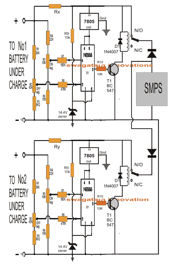
CIRCUIT DIAGRAM
CONNECTIONS
Motor driver ¨C
Pin ˇ®AˇŻ and ˇ®BˇŻ controls left side motor while Pin ˇ®CˇŻ and ˇ®DˇŻ controls right side of motor.
These four pins are connected to the four motors.
Pin ˇ®EˇŻ is to power IC(L298) which is taken from arduino (5v).
pin ˇ®FˇŻ is ground.
Pin ˇ®GˇŻ takes 12 volt power from battery via Vin pin of arduino.
Pins ˇ®HˇŻ, ˇ®IˇŻ, ˇ®JˇŻ and ˇ®KˇŻ receives logic from arduino.
DTMF ¨C
pin ˇ®aˇŻ is connected to 3.5 volt of arduino to power the IC (SC9270D).
Pin ˇ®bˇŻ is connected to ground.
The input of DTMF is taken from phone via jack.
The output in the form of binary data via (D0 ¨C D3) pins goes to arduino.
ARDUINO ¨C
the output of DTMF from (D0 ¨C D3) pins comes to digital pins of arduino.
We can connect this output to any of the four digital pins varying from (2 ¨C 13) in arduino.
Here we used pins 8, 9, 10 and 11.
Digital pins 2 and 3 of arduino are connected to pin number ˇ®HˇŻ and ˇ®IˇŻ of motor driver while pins 12 and 13 of arduino are connected to ˇ®JˇŻ and ˇŻKˇŻ.
The arduino is connected to a 12 volt battery.
Program CODE-
int x ; // initialising variables
int y ;
int z ;
int w ;
int a=20 ;
void setup()
{
pinMode(2,OUTPUT) ; //left motor
pinMode(3,OUTPUT) ; //left
pinMode(8,INPUT) ; // output from DO pin of DTMF
pinMode(9,INPUT) ; //output from D1 pin of DTMF
pinMode(10,INPUT) ; //output from D2 pin of DTMF
pinMode(11,INPUT) ; // output from D3 pin of DTMF
pinMode(12,OUTPUT) ; //right motor
pinMode(13,OUTPUT) ; //right
Serial.begin(9600);// begin serial communication between arduino and laptop
}
void decoding()// decodes the 4 bit binary number into decimal number
{
if((x==0)&&(y==0)&&(z==0)&&(w==0))
{
a=0;
}
if((x==0)&&(y==0)&&(z==1)&&(w==0))
{
a=2;
}
if((x==0)&&(y==1)&&(z==0)&&(w==0))
{
a=4;
}
if((x==0)&&(y==1)&&(z==1)&&(w==0))
{
a=6;
}
if((x==1)&&(y==0)&&(z==0)&&(w==0))
{
a=8;
}
}
void printing()// prints the value received from input pins 8,9,10 and 11 respectively
{
Serial.print(" x ");
Serial.print( x );
Serial.print(" y ");
Serial.print( y );
Serial.print(" z ");
Serial.print( z );
Serial.print(" w ");
Serial.print( w );
Serial.print(" a ");
Serial.print(a);
Serial.println();
}
void move_forward()// both side tyres of bot moves forward
{
digitalWrite(2,HIGH);
digitalWrite(3,LOW);
digitalWrite(12,HIGH);
digitalWrite(13,LOW);
}
void move_backward()//both side tyres of bot moves backward
{
digitalWrite(3,HIGH);
digitalWrite(2,LOW);
digitalWrite(13,HIGH);
digitalWrite(12,LOW);
}
void move_left()// only left side tyres move forward
{
digitalWrite(2,HIGH);
digitalWrite(3,LOW);
digitalWrite(12,LOW);
digitalWrite(13,HIGH);
}
void move_right()//only right side tyres move forward
{
digitalWrite(2,LOW);
digitalWrite(3,HIGH);
digitalWrite(12,HIGH);
digitalWrite(13,LOW);
}
void halt()// all motor stops
{
digitalWrite(2,LOW);
digitalWrite(3,LOW);
digitalWrite(12,LOW);
digitalWrite(13,LOW);
}
void reading()// take readings from input pins that are connected to DTMF D0, D1, D2 and D3 PINS.
{
x=digitalRead(8);
y=digitalRead(9);
z=digitalRead(10);
w=digitalRead(11);
}
void loop()
{
reading();
decoding();
if((x==0)&&(y==0)&&(z==1)&&(w==0))
{
move_forward();
reading();
decoding();
printing();
}
if((x==1)&&(y==0)&&(z==0)&&(w==0))
{
move_backward();
reading();
decoding();
printing();
}
if((x==0)&&(y==1)&&(z==0)&&(w==0))
{
move_left();
reading();
decoding();
printing();
}
if((x==0)&&(y==1)&&(z==1)&&(w==0))
{
move_right();
reading();
decoding();
printing();
}
if((x==0)&&(y==0)&&(z==0)&&(w==0))
{
halt();
reading();
decoding();
printing();
}
a=20;
printing();
}
CODE EXPLANATION
First of all, we initialise all variables before void setup.
In void setup, all pins to be used are assigned as input or output according to their purpose.
A new function ˇ°void decoding()ˇ± is made.
In this function all the binary input that we get from DTMF is decoded to decimal by arduino.
And variable assigned for this decimal value is a.
Another function ˇ°void printing()ˇ± is made.
This function is used to print input values from DTMF pins.
Similarly, five functions are required functions are required to perform the required task.
These functions are:
void move_left(); // robot turns left
void move_right() ; // robot turns right
void move_forward(); // robot moves forward
void move_backward() ; // robot moves backward
void halt() ; // robot stops
Now these functions are used in void loop function to do their task whenever they are called according to input from dialpad of cellphone.
For example:::
if((x==0)&&(y==0)&&(z==1)&&(w==0))
{
move_forward();
reading();
decoding();
printing();
}
hence when button 2 is pressed or 0010 is received on input pins, arduino decodes this and thus these functions do their work : move_forward();
reading();
decoding();
printing();
CIRCUIT WORKING
The controls which we have used in our project are as follows ¨C
2 ¨C To move forward
4 ¨C To turn left
6 ¨C To turn right
8 ¨C To move backwards
0 ¨C to stop
After making a call to the phone connected to the robot, the person opens his dial pad.
If ˇ®2ˇŻ is pressed.
The DTMF receives the input, decodes it in its binary equivalent number i.e.
ˇ®0010ˇŻ and sends it to digital pins of arduino.
The arduino then sends this code to the motor driver as we have programmed when the code will be ˇŻ0010ˇŻ, the motors will rotate in clockwise direction and hence our robot will move forward.
If ˇ®4ˇŻ is pressed then its equivalent code is ˇ®0100ˇŻ and according to the programming the left side motors will stop and only right side motors will rotate clockwise and hence our robot will turn left.
If ˇ®6ˇŻ is pressed then the right side motor will stop and only left side motors will rotate clockwise and hence our robot will turn right.
If ˇ®8ˇŻ is pressed then our motors will rotate in anticlockwise direction and thus our robot will move backward.
If ˇ®0ˇŻ is pressed then all our motors will stop and robot will not move.
In this project we have assigned a function to five dial pad numbers only.
We can add any type of other mechanism and assign a dial pad number to that mechanism to make an upgraded version of this project.
POINTS TO KEEP IN MIND
1 ¨C The jack should not be loose.
2 ¨C Phone keypad tones should be maximum.
3 ¨C Internet/ Wi-Fi of receiving phone should be closed to avoid interference effects.
4 ¨C Left pin (i.e.
pin ˇ®bˇŻ) of DTMF is ground and right pin (i.e.
pin ˇ®aˇŻ) is connected to 3.3v.
Prototype images of the cellphone controlled robot car circuit using DTMF
Video Demonstration of Cellphone controlled RC Car using DTMF
Introduction to EEPROM in Arduino
In this post we are going to understand what EEPROM is, how data is stored on built in EEPROM on Arduino boardˇŻs Microcontroller and also practically test how to write and read data on EEPROM by a couple of examples.
Why EEPROM?
Before we ask what EEPROM is? It is very important to know why EEPROM is used for storage in first place.
So that, we get clear idea on EEPROMs .
There are lot of storage devices available these days, ranging from magnetic storage devices like computer hard disks, old school cassette tape recorders, optical storage medium like CDs, DVDs, Blu-ray disks and solid state memory like SSD (Solid State Drive) for computers and Memory cards etc.
These are mass storage device which can store data such as music, videos, documents etc.
from as low as few Kilobytes to multi-Terabytes.
These are non-volatile memory which means, the data can be retained even after the power is cut-off to the storage medium.
The device which delivers ear soothing music or eye popping videos; such as computer or smartphone; stores some critical data such as configuration data, boot data, passwords, bio-metric data, login data etc.
These mentioned data cannot be stored in mass storage devices for security reasons and also these data could be modified by users unintentionally which could lead to malfunction of the device.
These data takes only few bytes to few Megabytes, connecting a conventional storage device like magnetic or optical medium to processor chips are not economically and physically feasible.
So, these critical data are stored in the processing chips itself.
The Arduino is no different from computer or smartphones.
There are several circumstances where we need to store some critical data which must not get erased even after the power is cut-off, for example sensor data.
By now, you would have got an idea why do we need EEPROM on microprocessors and microcontrollers chips.
What is EEPROM?
EEPROM stands for Electrically Erasable Programmable Read Only Memory.
It is also a non-volatile memory which can be read and write byte wise.
Reading and writing byte-level makes it different from other semiconductor memories.
For example flash memory: reading, writing and erasing data in block-wise manner.
A block can be few hundreds to thousands of bits, which is feasible for mass storage, but not for ˇ°Read Only Memoryˇ± operations in microprocessors and microcontrollers, which need to access byte by byte data.
On Arduino Uno board (ATmega328P) it has on board 1KB or 1024 bytes of EEPROM.
Each byte can be accessed individually; each byte has address ranging from 0 to 1023 (thatˇŻs total of 1024).
Address (0-1023) is a memory location where our data will be stored.
On each address you can store 8-bit data, numeric digits from 0 to 255. Our data is stored in binary form, so if we write number 255 into EEPROM it will store the digit as 11111111 in an address and if we store zero, it will store as 00000000.
You can also store text, special characters, alphanumeric characters etc.
by writing appropriate program.
The construction details and working are not discussed here which might make this article lengthy and we may make you sleepy.
Head towards YouTube or Google, there are interesting article/videos regarding constructional and working of EEPORM.
Do not confuse EEPROM with EPROM:
In a nutshell EPROM is an Electrically Programmable Read Only Memory meaning it can be programmed (store memory) electrically, but canˇŻt be erased electrically.
It utilizes bright shine of Ultraviolet light above storage chip which erases the stored data.
EEPROM came as replacement for EPROM and now hardly used in any electronic devices.
Do not confuse Flash Memory for EEPROM:
A flash memory is a semiconductor and non-volatile memory which is also electrically erasable and electrically programmable, in fact flash memory is derived from EEPROM.
But the block-wise memory access or in other words, the way of memory is accessed and its construction makes different from EEPROM.
Arduino Uno (ATmega328P Microcontroller) also sport 32KB of flash memory for program storage.
Lifespan of EEPROM:
Like any other electronic storage medium, EEPROM also has finite read, write, erase cycles.
But the problem is; it has one of the least lifespan compare to any other kind of semiconductor memory.
On ArduinoˇŻs EEPROM, Atmel claimed about 100000 (one lakh) write cycle per cell.
If your room temperature is lower the greater the lifespan of EEPROM.
Please note that reading data from EEPROM does not affect the lifespan significantly.
There are external EEPROM ICs which can be interfaced Arduino with ease with memory capacity ranging from 8 KB, 128KB, 256 KB etc.
with life span of about 1 million write cycles per cell.
ThatˇŻs concludes the EEPROM, now you would have gained enough theoretical knowledge about EEPROMs.
In the following section we will learn how to test the EEPROM on arduino practically.
How to Test EEPROM in Arduino
To implement this, all you need is a USB cable and Arduino Uno board, you are ready to go.
From the above explanations we understood that EEPROMs have Address where we store our data.
We can store 0 to 1023 locations in Arduino Uno.
Each location can accommodate 8-bits or one byte.
In this example we are going to store data in an address.
To reduce complexity of the program and to keep the program short as possible, we are going to store single digit integer (0 to 9) on an address from 0 to 9.
Program Code#1
Now, upload the code to Arduino:
//------------------Program Developed by R.GIRISH-------------------//
#include<EEPROM.h>
int inputAddress = 0;
int inputValue = 0;
int ReadData = 0;
boolean Readadd = true;
boolean Readval = true;
void setup()
{
Serial.begin(9600);
Serial.println("Enter the address (0 to 9)");
Serial.println("");
while(Readadd)
{
inputAddress = Serial.read();
if(inputAddress > 0)
{
inputAddress = inputAddress - 48;
Readadd = false;
}
}
Serial.print("You have selected Address: ");
Serial.println(inputAddress);
Serial.println("");
delay(2000);
Serial.println("Enter the value to be stored (0 to 9)");
Serial.println("");
while(Readval)
{
inputValue = Serial.read();
if(inputValue > 0)
{
inputValue = inputValue - 48;
Readval = false;
}
}
Serial.print("The value you entered is: ");
Serial.println(inputValue);
Serial.println("");
delay(2000);
Serial.print("It will be stored in Address: ");
Serial.println(inputAddress);
Serial.println("");
delay(2000);
Serial.println("Writing on EEPROM.....");
Serial.println("");
EEPROM.write(inputAddress, inputValue);
delay(2000);
Serial.println("Value stored successfully!!!");
Serial.println("");
delay(2000);
Serial.println("Reading from EEPROM....");
delay(2000);
ReadData = EEPROM.read(inputAddress);
Serial.println("");
Serial.print("The value read from Address ");
Serial.print(inputAddress);
Serial.print(" is: ");
Serial.println(ReadData);
Serial.println("");
delay(1000);
Serial.println("Done!!!");
}
void loop()
{
// DO nothing here.
}
//------------------Program Developed by R.GIRISH-------------------//
OUTPUT:
Once the code is uploaded, open the serial monitor.
It will ask you enter address ranging from 0 to 9. From the above output, I have entered address 3. So, I will be storing an integer value in the location (address) 3.
Now, it will prompt you to enter a single digit integer value ranging from 0 to 9. From the above output, I have entered value 5.
So, now the value 5 will be stored in the address location 3.
Once you enter the value, it will write the value on EEPROM.
It will show a success message, which means the value is stored.
After a couple of seconds it will read the value which is stored on the commented address and it will show the value on the serial monitor.
In conclusion, we have wrote and read the values from EEPROM of ArduinoˇŻs microcontroller.
Now, we are going to use the EEPROM for storing password.
We will be entering a 6 digit number (no less or no more) password, it will be stored in 6 different address (each address for each digit) and one additional address for storing ˇ°1ˇ± or ˇ°0ˇ±.
Once you enter the password, the additional address will store the value ˇ°1ˇ± indicating that password is set and the program will ask you to enter the password to turn ON the LED.
If the additional address stored value is ˇ°0ˇ± or any other value is present, it will ask you to create new 6 digit password.
By the above method, the program can identify whether you have already set a password or need to create a new password.
If the entered password is correct the build in LED at pin # 13 glows, if the entered password is incorrect, LED wonˇŻt glow and serial monitor will prompt that your password is wrong.
Open the serial monitor; it will prompt you to create a 6 digit number password.
Enter any 6 digit password and note it down and press enter.
Now the password has been stored.
You may either press the reset button or disconnect the USB cable from PC, which make the supply to Arduino board interrupted.
Now, reconnect the USB cable, open serial monitor, which will prompt you to enter the saved 6 digit password.
Enter the correct password the LED will glow.
If you want to change the password change the digit from the code:
int passExistAdd = 200;
The above line is the additional address which we discussed before.
Change anywhere from 6 to 1023. 0 to 5 addresses is reserved for storing 6 digit password.
Changing this additional address will fool the program that password is not created yet and prompt you to create a new 6 digit password.
If you have any questions regarding thisEEPROM in Arduino tutorial, please express in the comments, you may receive a quick reply.
Over Current Cut-off Power Supply Using Arduino
In this post we are going to construct a battery eliminator / DC variable power supply which will automatically cut-off the supply, if the current flow through the load exceeds the preset threshold level.
By Girish Radhakrishanan
Main Technical Features
The proposed over current cut-off power supply circuit using Arduinohas 16 X 2 LCD display, which is used to show case the voltage, current, power consumption and preset threshold current limit in real time.
Being an electronics enthusiast, we test our prototypes on a variable voltage power supply.
Most of us own a cheap variable power supply which might donˇŻt sport neither voltage measuring / current measuring feature nor short circuit or over current protection built in.
ThatˇŻs because power supply with these mentioned features can bomb on your wallet and will be overkilled for hobby usage.
Short circuit and over current flow is a problem for beginners to professionals and beginners are prone to this more often because of their inexperience, they might reverse the power supplyˇŻs polarity or connect the components in wrong way, etc.
These things can cause the current flow through the circuit unusually high, resulting in thermal runaway in semiconductor and passive components which results in destruction of valuable electronic components.
In these cases ohmˇŻs law turns into an enemy.
If you never made a short circuit or fried circuit, then congrats! You are one of few people who are perfect in electronics or you never try something new in electronics.
The proposed power supply project can protect the electronic components from such frying destruction, which will be cheap enough for an average electronics hobbyist and easy enough to construct one for who is slightly above beginner level.
The Design
The power supply has 3 potentiometers: one for adjusting the LCD display contrast, one for adjusting the output voltage ranging from 1.2 V to 15V and the last potentiometer is used for setting the current limit ranging from 0 to 2000 mA or 2 Ampere.
The LCD display will update you with four parameters every second: the voltage, current consumption, pre-set current limit and power consuming by the load.
The current consumption via load will be displayed in milliamps; the pre-set current limit will be displayed in milliamps and the power consumption will be displayed in milli-watts.
The circuit is divided into 3 parts: the power electronics, the LCD display connection and power measuring circuit.
These 3 stage may help the readers to understand the circuit better.
Now letˇŻs see the power electronics section which controls the output voltage.
Schematic diagram:
The 12v-0-12v / 3A transformer will be utilized for stepping down the voltage, the 6A4 diodes will convert the AC into DC voltage and the 2000uF capacitor will smooth out the choppy DC supply from diodes.
The LM 7809 fixed 9V regulator will convert the unregulated DC to regulated 9V DC supply.
The 9V supply will power the Arduino and relay.
Try to use a DC jack for arduinoˇŻs input supply.
DonˇŻt skip those 0.1uF ceramic capacitors which provide good stability for output voltage.
The LM 317 provides variable output voltage for the load which is to be connected.
You can adjust the output voltage by rotating the 4.7K ohm potentiometer.
That concludes the power section.
Now letˇŻs see the display connection:
Connection Details
There is nothing to explain here much, just wire up the Arduino and LCD display as per the circuit diagram.
Adjust the 10K potentiometer for better viewing contrast.
The above display shows the sample readings for the four parameters mentioned.
Power Measuring Stage
Now, letˇŻs see the power measurement circuit in detail.
The power measuring circuit comprises of voltmeter and ammeter.
The Arduino can measure voltage and current simultaneously by connecting the network of resistors as per the circuit diagram.
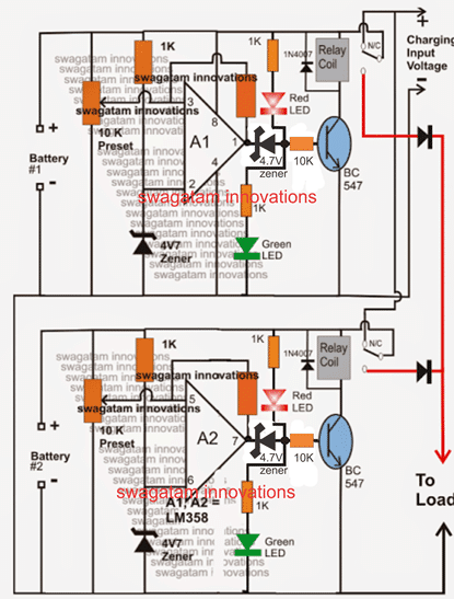
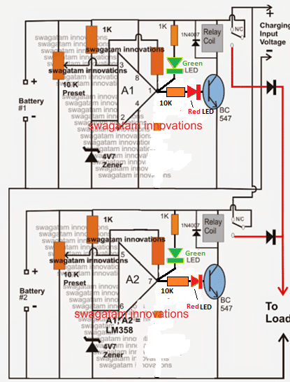
Relay Connection Details for the above Design:
The four 10 ohm resistors in parallel which forms 2.5 ohm shunt resistor which will be utilized for measuring the current flow through the load.
The resistors should be at least 2 watt each.
The 10k ohm and 100k ohm resistors helps the Arduino to measure voltage at the load.
These resistor can be one with normal wattage rating.
If you want to know more about the working of Arduino based ammeter and voltmeter check out these two links:
Voltmeter: https://www.homemade-circuits.com/2016/09/how-to-make-dc-voltmeter-using-arduino.html
Ammeter: https://www.homemade-circuits.com/2017/08/arduino-dc-digital-ammeter.html
The 10K ohm potentiometer is provided for adjusting the maximum current level at the output.
If the current flow through the load exceeds the pre-set current the output supply will be disconnected.
You can see the preset level in the display it will be mentioned as ˇ°LTˇ± (Limit).
Say for example: if you set the limit as 200, it will gives out current till 199mA.
If the current consumption gets equal to 200 mA or above the output will be immediately cut-off.
The output is turned on and off by the Arduino pin #7. When this pin is high the transistor energizes the relay which connects the common and normally open pins, which conducts the positive supply for the load.
The diode IN4007 absorbs the high voltage back EMF from the relay coil while switching the relay ON and OFF.
Program Code:
//------------------Program Developed by R.GIRISH------------------//
#include <LiquidCrystal.h>
#define input_1 A0
#define input_2 A1
#define input_3 A2
#define pot A3
LiquidCrystal lcd(12, 11, 5, 4, 3, 2);
int Pout = 7;
int AnalogValue = 0;
int potValue = 0;
int PeakVoltage = 0;
int value = 0;
int power = 0;
float AverageVoltage = 0;
float input_A0 = 0;
float input_A1 = 0;
float output = 0;
float Resolution = 0.00488;
float vout = 0.0;
float vin = 0.0;
float R1 = 100000;
float R2 = 10000;
unsigned long sample = 0;
int threshold = 0;
void setup()
{
lcd.begin(16,2);
Serial.begin(9600);
pinMode(input_3, INPUT);
pinMode(Pout, OUTPUT);
pinMode(pot, INPUT);
digitalWrite(Pout, HIGH);
}
void loop()
{
PeakVoltage = 0;
value = analogRead(input_3);
vout = (value * 5.0) / 1024;
vin = vout / (R2/(R1+R2));
if (vin < 0.10)
{
vin = 0.0;
}
for(sample = 0; sample < 5000; sample ++)
{
AnalogValue = analogRead(input_1);
if(PeakVoltage < AnalogValue)
{
PeakVoltage = AnalogValue;
}
else
{
delayMicroseconds(10);
}
}
input_A0 = PeakVoltage * Resolution;
PeakVoltage = 0;
for(sample = 0; sample < 5000; sample ++)
{
AnalogValue = analogRead(input_2);
if(PeakVoltage < AnalogValue)
{
PeakVoltage = AnalogValue;
}
else
{
delayMicroseconds(10);
}
}
potValue = analogRead(pot);
threshold = map(potValue, 0, 1023, 0, 2000);
input_A1 = PeakVoltage * Resolution;
output = (input_A0 - input_A1) * 100;
output = output * 4;
power = output * vin;
while(output >= threshold || analogRead(input_1) >= 1010)
{
digitalWrite(Pout, LOW);
while(true)
{
lcd.clear();
lcd.setCursor(0,0);
lcd.print("Power Supply is");
lcd.setCursor(0,1);
lcd.print("Disconnected.");
delay(1500);
lcd.clear();
lcd.setCursor(0,0);
lcd.print("Press Reset the");
lcd.setCursor(0,1);
lcd.print("Button.");
delay(1500);
}
}
while(output >= threshold || analogRead(input_2) >= 1010)
{
digitalWrite(Pout, LOW);
while(true)
{
lcd.clear();
lcd.setCursor(0,0);
lcd.print("Power Supply is");
lcd.setCursor(0,1);
lcd.print("Disconnected.");
delay(1500);
lcd.clear();
lcd.setCursor(0,0);
lcd.print("Press Reset the");
lcd.setCursor(0,1);
lcd.print("Button.");
delay(1500);
}
}
lcd.clear();
lcd.setCursor(0,0);
lcd.print("V=");
lcd.print(vin);
lcd.setCursor(9,0);
lcd.print("LT=");
lcd.print(threshold);
lcd.setCursor(0,1);
lcd.print("I=");
lcd.print(output);
lcd.setCursor(9,1);
lcd.print("P=");
lcd.print(power);
Serial.print("Volatge Level at A0 = ");
Serial.println(analogRead(input_1));
Serial.print("Volatge Level at A1 = ");
Serial.println(analogRead(input_2));
Serial.print("Voltage Level at A2 = ");
Serial.println(analogRead(input_3));
Serial.println("------------------------------");
}
//------------------Program Developed by R.GIRISH------------------//
By now, you would have gained enough knowledge to construct a power supply which protect you valuable electronic components and modules.
If you have any specific question regarding this over current cut-off power supply circuit using Arduino feel free to ask in comment section, you may receive a quick reply.
Make this Advanced Digital Ammeter using Arduino
In this post we are going to construct a digital ammeter using 16 x 2 LCD display and Arduino.
We will understand the methodology of measuring current using a shunt resistor and implement a design based on Arduino.
The proposed digital ammeter can measure current ranging from 0 to 2 Ampere (absolute maximum) with reasonable accuracy.
How Ammeters Work
There are two types of ammeters: Analog and digital, their workings are way different from each other.
But, they both have one concept in common: A shunt resistor.
A shunt resistor is a resistor with very small resistance placed between the source and the load while measuring the current.
LetˇŻs see how an analog ammeter works and then it will be easier to understand the digital one.
A shunt resistor with very low resistance R and assume some kind analog meter is connected across the resistor whoˇŻs deflection is directly proportional to voltage through the analog meter.
Now letˇŻs pass some amount of current from left hand side.
i1 is the current before entering the shunt resistor R and i2 will be the current after passing through shunt resistor.
The current i1 will be greater than i2 since it dropped a fraction of current through shunt resistor.
The current difference between the shunt resistor develops very small amount of voltage at V1 and V2.
The amount of voltage will be measured by that analog meter.
The voltage developed across the shunt resistor depends on two factors: the current flowing through the shunt resistor and the value of the shunt resistor.
If the current flow is greater through the shunt the voltage developed is more.
If the value of the shunt is high the voltage developed across the shunt is more.
The shunt resistor must be very tiny value and it must possess higher wattage rating.
A small value resistor ensures that the load is getting adequate amount of current and voltage for normal operation.
Also the shunt resistor must have higher wattage rating so that it can tolerate the higher temperature while measuring the current.
Higher the current through the shunt more the heat is generated.
By now you would have got the basic idea, how an analog meter works.
Now letˇŻs move on to digital design.
By now we know that a resistor will produce a voltage if there is a current flow.
From the diagram V1 and V2 are the points, where we take the voltage samples to the microcontroller.
Calculating Voltage to Current Conversion
Now letˇŻs see the simple math, how can we convert the produced voltage to current.
The ohmˇŻs law: I = V/R
We know the value of the shunt resistor R and it will be entered in the program.
The voltage produced across the shunt resistor is:
V = V1 ¨C V2
Or
V = V2 ¨C V1 (to avoid negative symbol while measuring and also negative symbol depend on direction of current flow)
So we can simplify the equation,
I = (V1 ¨C V2)/R
Or
I = (V2 - V1)/R
One of the above equations will be entered in the code and we can find the current flow and will be displayed in the LCD.
Now letˇŻs see how to choose the shunt resistor value.
The Arduino has built in 10 bit analog to digital converter (ADC).
It can detect from 0 to 5V in 0 to 1024 steps or voltage levels.
So the resolution of this ADC will be 5/1024 = 0.00488 volt or 4.88 millivolt per step.
So 4.88 millivolt/2 mA (minimum resolution of ammeter) = 2.44 or 2.5 ohm resistor.
We can use four 10 ohm, 2 Watt resistor in parallel to get 2.5 ohm which was tested in the prototype.
So, how can we say the maximum measurable range of the proposed ammeter which is 2 Ampere.
The ADC can measure from 0 to 5 V only i.e.
. Anything above will damage the ADC in the microcontroller.
From the tested prototype what we have observed that, at the two analog inputs from point V1 and V2; when the current measured value X mA, the analog voltage reads X/2 (in serial monitor).
Say for example, if the ammeter reads 500 mA the analog values on serial monitor reads 250 steps or voltage levels.
The ADC can tolerate up to 1024 steps or 5 V maximum, So when the ammeter reads 2000 mA, the serial monitor reads 1000 steps approx.
which is near to 1024.
Anything above 1024 voltage level will damage the ADC in Arduino.
To avoid this just before 2000 mA a warning message will prompt on LCD saying to disconnect the circuit.
By now you would have understood how the proposed ammeter works.
Now letˇŻs move on to constructional details.
Schematic diagram:
The proposed circuit is very simple and beginner friendly.
Construct as per the circuit diagram.
Adjust the 10K potentiometer to adjust display contrast.
You can power the Arduino from USB or via DC jack with 9 V batteries.
Four 2 watt resistors will dissipate the heat evenly than using one 2.5 ohm resistor with 8- 10 watt resistor.
When no current is passing the display may read some small random value which you may ignore it, this might be due to stray voltage across measuring terminals.
NOTE: DonˇŻt reverse the input load supply polarity.
In this project we are going to interface a digital potentiometer with arduino.
In this demonstration potentiometer MCP41010 is used but you can use any digital potentiometer of MC41** series.
By Ankit Negi
INTRODUCTION TO MC41010
Digital potentiometers are just like any analog potentiometer with three terminals with only one difference.
Whereas in analog one you have to manually change the wiper position, In case of digital potentiometer wiper position is set according to the signal given to potentiometer using any microcontroller or microprocessor.
FIG.
MC41010 IC pinout
MC41010 is an 8 pin dual in line package IC.
Just like any analog potentiometer this IC comes in 5k, 10k, 50k, and 100k.
In this circuit 10k potentiometer is used
MC4131 have following 8 terminals:
Pin no.
Pin Name Little description
1 CS This pin is used to select the slave or peripheral connected to arduino.
If this is
Low then MC41010 is selected and if this is high then MC41010 is deselected.
2 SCLK Shared/Serial Clock, arduino gives clock for initialization of data transfer from
Arduino to IC and vice versa.
3 SDI/SDO Serial data is transferred between arduino and IC through this pin
4 VSS Ground terminal of arduino is connected to this pin of IC.
5 PA0 This is one terminal of the potentiometer.
6 PW0 This terminal is wiper terminal of the potentiometer( to change resistance)
7 PB0 This is another terminal of the potentiometer.
8 VCC Power to IC is given through this pin.
This IC contains only one potentiometer.
Some IC have at most two potentiometer inbuilt.
This
The value of the resistance between wiper and any other terminal is changed in 256 steps, from 0 to 255. Since we are using a 10k resistor value of resistor is changed in steps of:
10k/256= 39 ohms per step between 0 and 255
COMPONENTS
We need following components for this project.
1. ARDUINO
2. MC41010 IC
3. 220 OHM RESISTOR
4. LED
5. CONNECTING WIRES
Make connections as shown in fig.
1. Connect cs pin to digital pin 10.
2. Connect SCK pin to digital pin 13.
3. Connect SDI/SDO pin to digital pin 11.
4. VSS to ground pin of arduino
5. PA0 to 5v pin of arduino
6. PB0 to ground of arduino
7. PWO to analog pin A0 of arduino.
8. VCC to 5 v of arduino.
PROGRAM CODE 1
This code prints the voltage change across wiper terminal and ground on Serial Monitor of Arduino IDE.
#include <SPI.h>
int CS = 10 ; // initialising variable CS pin as pin 10 of arduino
int x ; // initialising variable x
float Voltage ; // initialising variable voltage
int I ; // this is the variable which changes in steps and hence changes resistance accordingly.
void setup()
{
pinMode (CS , OUTPUT) ; // initialising 10 pin as output pin
pinMode (A0, INPUT) ; // initialising pin A0 as input pin
SPI.begin() ; // this begins Serial peripheral interfece
Serial.begin(9600) ; // this begins serial communications between arduino and ic.
}
void loop()
{
for (int i = 0; i <= 255; i++)// this run loops from 0 to 255 step with 10 ms delay between each step
{
digitalPotWrite(i) ; // this writes level i to ic which determines resistance of ic
delay(10);
x = analogRead(A0) ; // read analog values from pin A0
Voltage = (x * 5.0 )/ 1024.0;// this converts the analog value to corresponding voltage level
Serial.print("Level i = " ) ; // these serial commands print value of i or level and voltage across wiper
Serial.print(i) ; // and gnd on Serial monitor of arduino IDE
Serial.print("\t Voltage = ") ;
Serial.println(Voltage,3) ;
}
delay(500);
for (int i = 255; i >= 0; i--) // this run loops from 255 to 0 step with 10 ms delay between each step
{
digitalPotWrite(i) ;
delay(10) ;
x = analogRead(A0) ;
Voltage = (x * 5.0 )/ 1024.0 ; // this converts the analog value to corresponding voltage level
Serial.print("Level i = " ) ; // these serial commands print value of i or level and voltage across wiper
Serial.print(i); // and gnd on Serial monitor of arduino IDE
Serial.print("\t Voltage = ");
Serial.println(Voltage,3);
}
}
int digitalPotWrite(int value) // this block is explained in coding section
{
digitalWrite(CS, LOW);
SPI.transfer(B00010001);
SPI.transfer(value);
digitalWrite(CS, HIGH);
EXPLAINING CODE 1:
To use digital potentiometer with arduino you need to include SPI library first which is provided in arduino IDE itself.
Just call the library with this command:
#include <SPI.h>
In void setup, pins are assigned as output or input.
And commands to begin SPI and serial communication between arduino and ic is also given which are:
SPI.begin(); and
Serial.begin(9600);
In void loop, for loop is used to change the resistance of digital pot in total 256 steps.
First from 0 to 255 and then again back to 0 with 10 milliseconds delay between each step:
for (int i = 0; i <= 255; i++) and
for (int i = 255; i >= 0; i--)
digitalPotWrite(i) function writes theese value to change resistance at particular address of ic.
Resistance between wiper and end terminal can be calculated using these formulae:
R1= 10k*(256-level)/256 + Rw
And
R2= 10k*level/256 + Rw
Here R1= resistance between wiper and one terminal
R2= resistance between wiper and other terminal
Level = step at a particular instant ( variable ˇ°Iˇ± used in for loop)
Rw= resistance of wiper terminal ( can be found in datasheet of the ic )
Using digitalPotWrite() function the digital potentiometer chip is selected by assigning LOW voltage to CS pin.
Now as the ic is selected, an address must be called on which data will be written.
In the last portion of code :
SPI.transfer(B00010001);
Address is called which is B00010001 to select the wiper terminal of the ic on which data will be written.
And hence for loopˇŻs value i.e, i is written to change the resistance.
CIRCUIT WORKING:
As long as value of i keeps changing input to A0 pin of arduino also keeps changing between 0 and 1023. This happens because wiper terminal is directly connected to A0 pin, and other terminal of potentiometer are connected to 5volt and ground respectively.
Now when resistance changes so do voltage across it which is directly taken by arduino as input and thus we get a voltage value on serial monitor for a particular value of resistance.
SIMULATION 1:
These are some simulation pictures for this circuit at various values of i:
Now just connect an led in series with 220ohm resistor to wiper terminal of IC as shown in figure.
CODE 2:
#include <SPI.h>
int CS = 10;
int x;
float Voltage;
int i;
void setup()
{
pinMode (CS , OUTPUT);
pinMode (A0, INPUT);
SPI.begin();// this begins Serial peripheral interfece
}
void loop()
{
for (int i = 0; i <= 255; i++)// this run loops from 0 to 255 step with 10 ms delay between each step
{
digitalPotWrite(i);// this writes level i to ic which determines resistance of ic
delay(10);
}
delay(500);
for (int i = 255; i >= 0; i--)// this run loops from 255 to 0 step with 10 ms delay between each step
{
digitalPotWrite(i);
delay(10);
}
}
int digitalPotWrite(int value)// this block is explained in coding section
{
digitalWrite(CS, LOW);
SPI.transfer(B00010001);
SPI.transfer(value);
digitalWrite(CS, HIGH);
}
EXPLAINING CODE 2:
This code is similar to code 1 except that there are no serial commands in this code.
So no values will be printed on serial monitor.
WORKING EXPLANATION
Since led is connected between wiper terminal and ground as resistance changes so do voltage across led.
And hence as resistance across which led is connected rises from 0ohm to maximum so do brightness of led.
Which again slowly fade away due to decrease in resistance from maximum to 0v.
Simulation2
Simulation3
Digital Capacitance Meter Circuit Using Arduino
In this post we are going to construct a digital capacitance meter circuit using Arduino which can measure capacitance of capacitors ranging from 1 microfarad to 4000 microfarad with reasonable accuracy.
Introduction
We measure value of the capacitors when the values written on the capacitorˇŻs body is not legible, or to find the value of the ageing capacitor in our circuit which need to be replaced soon or later and there are several other reasons to measure the capacitance.
To find the capacitance we can easily measure using a digital multimeter, but not all multimeters have capacitance measuring feature and only the expensive multimeters have this functionality.
So here is a circuit which can be constructed and used with ease.
We are focusing on capacitors with larger value from 1 microfarad to 4000 microfarad which are prone to lose its capacitance due to ageing especially electrolytic capacitors, which consist of liquid electrolyte.
Before we go into circuit details, letˇŻs see how we can measure capacitance with Arduino.
Most Arduino capacitance meter relies on RC time constant property.
So what is RC time constant?
The time constant of RC circuit can be defined as time taken for the capacitor to reach 63.2 % of the full charge.
Zero volt is 0 % charge and 100% is capacitorˇŻs full voltage charge.
The product of value of resistor in ohm and value of capacitor in farad gives Time constant.
T = R x C
T is the Time constant
By rearranging the above equation we get:
C = T/R
C is the unknown capacitance value.
T is the time constant of RC circuit which is 63.2 % of full charge capacitor.
R is a known resistance.
The Arduino can sense the voltage via analog pin and the known resistor value can be entered in the program manually.
By applying the equation C = T/R in the program we can find the unknown capacitance value.
By now you would have an idea how we can find the value of unknown capacitance.
In this post I have proposed two kinds of capacitance meter, one with LCD display and another using serial monitor.
If you are frequent user of this capacitance meter it is better go with LCD display design and if you are not frequent user better go with serial monitor design because it save you some bucks on LCD display.
Now letˇŻs move on to circuit diagram.
Serial Monitor based capacitance meter:
As you can see the circuit is very simple just a couple of resistors are needed to find the unknown capacitance.The 1K ohm is the known resistor value and the 220 ohm resistor utilized for discharging the capacitor while measurement process takes place.The Arduino sense the rising and decreasing voltage on pin A0 which is connected between 1K ohm and 220 ohm resistors.Please take care of the polarity if you are using polarized capacitors such as electrolytic.Program://-----------------Program developed by R.Girish------------------//
const int analogPin = A0;
const int chargePin = 7 ;
const int dischargePin = 6;
float resistorValue = 1000 // Value of known resistor in ohm
unsigned long startTime;
unsigned long elapsedTime;
float microFarads;
void setup()
{
Serial.begin(9600);
pinMode(chargePin, OUTPUT);
digitalWrite(chargePin, LOW);
}
void loop()
{
digitalWrite(chargePin, HIGH);
startTime = millis();
while(analogRead(analogPin) < 648){}
elapsedTime = millis() - startTime;
microFarads = ((float)elapsedTime / resistorValue) * 1000;
if (microFarads > 1)
{
Serial.print("Value = ");
Serial.print((long)microFarads);
Serial.println(" microFarads");
Serial.print("Elapsed Time = ");
Serial.print(elapsedTime);
Serial.println("mS");
Serial.println("--------------------------------");
}
else
{
Serial.println("Please connect Capacitor!");
delay(1000);
}
digitalWrite(chargePin, LOW);
pinMode(dischargePin, OUTPUT);
digitalWrite(dischargePin, LOW);
while(analogRead(analogPin) > 0) {}
pinMode(dischargePin, INPUT);
}
//-----------------Program developed by R.Girish------------------//Upload the above code to Arduino with completed hardware setup, initially donˇŻt connect the capacitor.
Open the serial monitor; it says ˇ°Please connect capacitorˇ±.
Now connect a capacitor, its capacitance will be displayed as illustrated below.
It also shows the time taken to reach 63.2% of the capacitorˇŻs full charge voltage, which is shown as elapsed time.
Circuit diagram for LCD based capacitance meter:
The above schematic is connection between LCD display and Arduino.
The 10K potentiometer is provided for adjusting the contrast of the display.
Rest of the connections are self-explanatory.
The above circuit is exactly same as serial monitor based design; you just need to connect LCD display.
Program for LCD based capacitance meter:
//-----------------Program developed by R.Girish------------------//
#include<LiquidCrystal.h>
LiquidCrystal lcd(12,11,5,4,3,2);
const int analogPin = A0;
const int chargePin = 7 ;
const int dischargePin = 6;
float resistorValue = 1000; // Value of known resistor in ohm
unsigned long startTime;
unsigned long elapsedTime;
float microFarads;
void setup()
{
Serial.begin(9600);
lcd.begin(16,2);
pinMode(chargePin, OUTPUT);
digitalWrite(chargePin, LOW);
lcd.clear();
lcd.setCursor(0,0);
lcd.print(" CAPACITANCE");
lcd.setCursor(0,1);
lcd.print(" METER");
delay(1000);
}
void loop()
{
digitalWrite(chargePin, HIGH);
startTime = millis();
while(analogRead(analogPin) < 648){}
elapsedTime = millis() - startTime;
microFarads = ((float)elapsedTime / resistorValue) * 1000;
if (microFarads > 1)
{
lcd.clear();
lcd.setCursor(0,0);
lcd.print("Value = ");
lcd.print((long)microFarads);
lcd.print(" uF");
lcd.setCursor(0,1);
lcd.print("Elapsed:");
lcd.print(elapsedTime);
lcd.print(" mS");
delay(100);
}
else
{
lcd.clear();
lcd.setCursor(0,0);
lcd.print("Please connect");
lcd.setCursor(0,1);
lcd.print("capacitor !!!");
delay(500);
}
digitalWrite(chargePin, LOW);
pinMode(dischargePin, OUTPUT);
digitalWrite(dischargePin, LOW);
while(analogRead(analogPin) > 0) {}
pinMode(dischargePin, INPUT);
}
//-----------------Program developed by R.Girish------------------//
With the completed hardware setup upload the above code.
Initially donˇŻt connect the capacitor.
The display shows ˇ°Please connect capacitor!!!ˇ± now you connect the capacitor.
The display will show the capacitorˇŻs value and elapsed time taken to reach 63.2% of full charge capacitor.
AuthorˇŻs Prototype:
Arduino Tachometer Circuit for Precise Readings
A tachometer is a device that measures the RPM or angular velocity of a rotating body.
It differs from speedometer and odometer as these devices deal with linear or tangential velocity of the body while tachometer a.k.a.
ˇ°tachˇ± deals with more fundamental the RPM.
By Ankit Negi
Tachometer is composed of a counter and a timer both of these working together provides the RPM.In our project we are going to do same, using our Arduino and some sensors we will setup both a counter and a timer and develop our handy and easy tach.
Prerequisites
Counter is nothing but a device or setup that can count any certain regular occurring event like passing of a dot in disc while in rotation.
Initially the counters were built using the mechanical arrangement and linkages like gears, ratchets, springs etc.
But now we are using counter having more sophisticated and highly precise sensors and electronics.Timer is an electronic element that is able to measure the time interval between events or measure time.
In our Arduino Uno there are timers that not only keep track of time but also maintain some of the important functions of Arduino.
In Uno we have 3 timers named Timer0, Timer1 and Timer2. These timers have following functions- Timer0- For Uno functions like delay(), millis(), micros() or delaymicros().
Timer1- For the working of servo library.
Timer2- For functions like tone(), notone().
Along with these functions these 3 timers are also responsible for generating the PWM Output when analogWrite() command is used in the PMW designated pin.
Concept of Interrupts
In Arduino Uno a hidden tool is present which can give access to a whole lot of functioning to us known as Timer Interrupts.Interrupt is a set of events or instructions that are executed when called interrupting the current functioning of the device, i.e.
no matter what codes your Uno was executing before but once an Interrupt is called Arduino execute the instruction mentioned in the Interrupt.
Now Interrupt can be called at certain condition defined by the user using an inbuilt Arduino Syntax.We will be using this Interrupt in our project that makes our tachometer more resolute as well as more precise than the other Tachometer project present around the web.
Components required for this Tachometer project using Arduino
Hall Effect Sensor (Fig.1)
Arduino Uno
Small magnet
Jumper wires
Rotating Object (Motor shaft)
Circuit Setup
The setup for creating is as follows-
In the shaft whose rotation speed is to be measured is fitted with a small magnet using glue gun or electrical tape.
Hall Effect sensor has a detector in front and 3 pins for connections.
The Vcc and Gnd pins are connected to 5V and Gnd pin of Arduino respectively.
The Output pin of the sensor is connected to the digital pin 2 of the Uno to provide the input signal.
All components are fixed in a mount board and Hall detector is pointed out from the board.
Programming
int sensor = 2; // Hall sensor at pin 2
volatile byte counts;
unsigned int rpm; //unsigned gives only positive values
unsigned long previoustime;
void count_function()
{ /*The ISR function
Called on Interrupt
Update counts*/
counts++;
}
void setup() {
Serial.begin(9600);
//Intiates Serial communications
attachInterrupt(0, count_function, RISING); //Interrupts are called on Rise of Input
pinMode(sensor, INPUT); //Sets sensor as input
counts= 0;
rpm = 0;
previoustime = 0; //Initialise the values
}
void loop()
{
delay(1000);//Update RPM every second
detachInterrupt(0); //Interrupts are disabled
rpm = 60*1000/(millis() - previoustime)*counts;
previoustime = millis(); //Resets the clock
counts= 0; //Resets the counter
Serial.print("RPM=");
Serial.println(rpm); //Calculated values are displayed
attachInterrupt(0, count_function, RISING); //Counter restarted
}
Upload the code.
Know the code
Our tachometer uses Hall Effect Sensor; Hall Effect sensor is based on Hall effect named after its discoverer Edwin Hall.
Hall Effect is phenomenon of generation of voltage across a current carrying conductor when a magnetic field is introduced perpendicular to the flow of current.
This voltage generated due this phenomenon help in Input signal generation.As mentioned Interrupt will be used in this project, to call Interrupt we have to setup some condition.
Arduino Uno has 2 conditions for calling for Interrupts-
RISING- When used this, Interrupt are called every time when the Input signal goes from LOW to HIGH.
FALING-When used this, Interrupt are called when signal goes from HIGH to LOW.
We have used the RISING, what happens is that when the magnet placed in the shaft or rotating object come close to Hall detector Input signal is generated and Interrupt are called in, Interrupt initiates the Interrupt Service Routine(ISR) function, which include increment in the counts value and thus count takes place.
We have used the millis() function of Arduino and previoustime (variable) in correspondence to setup the timer.
The RPM thus is finally calculated using the mathematical relation-
RPM= Counts/Time taken Converting the milliseconds to minutes and rearrangement we gets to the formula= 60*1000/(millis() - previoustime)*counts.
The delay(1000) determines the time interval after which the value of RPM will be updated on the screen, you can adjust this delay according to your needs.
This value of RPM obtained can be further used to calculate the tangential velocity of the rotating object using the relation- v= (3.14*D*N)/60 m/s.
The value of RPM can also be used to calculate the distance travelled by a rotating wheel or disc.
Instead of printing values to Serial monitor this device can be made more useful by connecting a LCD display (16*2) and battery for better usage.
Transformerless AC Voltmeter Circuit Using Arduino
In this article we learn how to make a transformerless AC voltmeter using Arduino.
Making an analog voltmeter is not an easy task as to build one you must have good knowledge of physical quantities like torque, speed; which can be very difficult when it comes to their practical applications.
By Ankit Negi
But a digital voltmeter in comparison to analog voltmeter can be made quickly and that too with very little effort.
Now a dayˇŻs digital voltmeter can be made using a microcontroller or development board like arduino by using 4-5 line code.
Why this AC Voltmeter circuit is different?
If you go to Google and search ˇ°AC voltmeter using arduinoˇ±; you will find many circuits all over the internet.
But in almost all those circuits you will find a transformer being used.
Now using a transformer is not a good idea if you want to make a reliable and efficient voltmeter since it makes circuit bulky and heavy.
Circuit in this project solves this problem completely by replacing the transformer from a high watt voltage divider circuit.
This circuit can be easily made on a small breadboard within minutes.Components required:
For making this project you need following components:
1. Arduino
2. 100k ohm resistor (2 watt)
3. 1k ohm resistor (2 watt)
4. 1N4007 diode
5. One zener diode 5 volts
6. 1 uf capacitor
7. Connecting wires
CIRCUIT DIAGRAM:
Make connections as shown in circuit diagram.
A) Make a voltage divider using resistors keeping in mind that 1 k ohm resistor should be connected to ground.
B) Connect diodeˇŻs p- terminal directly after 1 k ohm resistor as shown in fig.
and its n- terminal to 1 uf capacitor.
C) DonˇŻt forget to connect zener diode in parallel to the capacitor( explained below)
D) Connect a wire from positive terminal of capacitor to the analog pin A0 of arduino.
E) ** do connect the ground pin of arduino to the overall ground else circuit will not work.
OBJECTIVE OF ARDUINO::
Well you can use any microcontroller, but I have used arduino due to its easy IDE.
Basically function of arduino or any microcontroller here is to take voltage across 1 k ohm resistor as analog input and convert that value into mains a.c.
voltage value by using a formula (explained in working section).
Arduino further print this mains value on serial monitor or laptop screen.
VOLTAGE DIVIDER CIRCUIT:
As already mentioned in component section, resistors (which makes up a voltage divider circuit) must be of high power rating as we are going to connect them directly to mains a.c supply.
And hence this voltage divider circuit replaces the transformer.
Since arduino can take maximum of 5v as analog input, voltage divider circuit is used to split mains high voltage into low voltage (less than 5v).LetˇŻs make an assumption that mains supply voltage is 350 volts ( r.m.s )
Which gives maximum or peak voltage = 300*1.414= 494.2 volts
So peak voltage across 1 k ohm resistor is = (494.2volts/101k)*1k = 4.9volts ( maximum )
Note:* but even for 350 r.m.s this 4.9 volts is not r.m.s that means in reality voltage on analog pin of arduino will be less than 4.9 v.
Hence from these calculations it is observed that this circuit can safely measure a.c voltage around 385 r.m.s.
WHY DIODE?
Since arduino cannot take negative voltage as input, itˇŻs very important to remove negative part of input a.c sin wave across 1 k ohm resistor.
And to do so it is rectified using a diode.
You can also use a bridge rectifier for better results.
WHY CAPACITOR?
Even after rectification there are ripples present in wave and to remove such ripples, a capacitor is being used.
Capacitor smooth out the voltage before feeding it to arduino.
WHY ZENER DIODE
Voltage greater than 5 volts can damage arduino.
Hence to protect it, a 5 v zener diode is used.
If a.c mains voltage increases beyond 380 volts i.e.
greater than 5 volts on analog pin, breakdown of zener diode will occur.
Thus shorting the capacitor to ground.
This ensures safety of arduino.
CODE:
Burn this code in your arduino:
int x;// initialise variable x
float y;//initialise variable y
void setup()
{
pinMode(A0,INPUT); // set pin a0 as input pin
Serial.begin(9600);// begin serial communication between arduino and pc
}
void loop()
{
x=analogRead(A0);// read analog values from pin A0 across capacitor
y=(x*.380156);// converts analog value(x) into input ac supply value using this formula ( explained in woeking section)
Serial.print(" analaog input " ) ; // specify name to the corresponding value to be printed
Serial.print(x) ; // print input analog value on serial monitor
Serial.print(" ac voltage ") ; // specify name to the corresponding value to be printed
Serial.print(y) ; // prints the ac value on Serial monitor
Serial.println();
}
Understanding code:
1. VARIABLE x:
X is the input analog value received (voltage) from pin A0 as specified in the code i.e.,
x = pinMode (A0,INPUT) ; // set pin a0 as input pin
2. VARIABLE Y:
To arrive at this formula y=(x*.380156), first we have to do some sort of calculations:
This circuit here always provides voltage less than the actual value on pin A0 of arduino due to capacitor and diode.
Which means voltage on analog pin is always less than the voltage across 1 k ohm resistor.
Hence we have to find out that value of input ac voltage at which we get 5 volts or 1023 analog value on pin A0. By hit and trial method, that value is around 550 volts (peak) as shown in simulation.
In r.m.s 550 peak volts = 550/1.414= 388.96 volts r.m.s.
Hence for this r.m.s value we obtain 5 volts on pin A0. So this circuit can measure maximum of 389 volts.
Now for 1023 analog value on pin A0 --- 389 a.c volts = y
Which gives, for any analog value(x); y = (389/1023)*x a.c volts
OR y =.38015*x a.c volts
You can clearly observe in fig that printed a.c value on serial monitor is also 389 volts
Printing required values on screen::
We require two values to be printed on serial monitor as shown in the simulation picture:
1. Analog input value received by analog pin A0 as specified in the code:
Serial.print(" analaog input ") ; // specify name to the corresponding value to be printed
Serial.print(x) ; // print input analog value on serial monitor
2. Actual value of ac voltage from mains as specified in the code:
Serial.print(" ac voltage ") ; // specify name to the corresponding value to be printed
Serial.print(y) ; // prints the ac value on Serial monitor
WORKING OF THIS TRANSFORMERLESS AC VOLTMETER USING ARDUINO
1. Voltage divider circuit converts or step down the mains ac voltage into corresponding low voltage value.
2. This voltage after rectification is taken by analog pin of arduino and by using formula
y = 0.38015*x a.c volts is converted into actual mains a.c value voltage.
3. This converted value is then printed on serial monitor of arduino IDE.
SIMULATION:
To see how close the printed value on screen to the actual a.c value, simulation is run for different values of a.c voltages :
A) 220 volts or 311 amplitude
B) 235 volts or 332.9 amplitude
C) 300 volts or 424.2
Hence from the following results it is observed that for 220 a.c supply, arduino shows 217 volts.
And as this a.c value increases, results of simulation become more accurate that is more close to the input a.c value.
LCD 220V Mains Timer Circuit ¨C Plug and Play Timer
In this post we are going to make an LCD 220 V mains operated timer using Arduino whose countdown time can be witnessed via 16 x 2 LCD display.
Introduction
The proposed LCD timer circuit is general purpose timer with display and few buttons for setting the time.
Once the time is set output goes high and starts countdown the time and when it reach 00:00:00 (Hour: Minute: Seconds) the output goes low.
You may modify this project for your customized needs.
Now back to the project.
We always worry on our electrical or electronic devices which ran for too long just because we forget them to switch off them.
Time critical electrical and electronic devices like electric cooker, low profile battery chargers, heaters etc.
need to be switched off at right moment otherwise we may end up reducing the life time of the gadgets or the processed end item such as food will be unpleasant to consume.
Low profile battery chargers might not have timer or battery monitoring system which might damage the batteryˇŻs life span if we left on charge for long time.
We can say hundreds of examples like these, to escape from such bad results a timer socket can be used.
A timer socket is a simple timer which is connected to AC socket and the time critical devices will be connected at output of the timer socket.
The user has to input the time using button or dials for how long the connected devices should be powered.
Once the pre-set time is reached the device will be cut-off from the power supply.
The Design:
The proposed LCD socket timer project consists of Arduino which acts as brain of the project, a 16 x 2 LCD display which shows the remaining time, three buttons for setting the time and a relay for connecting and disconnecting the output AC supply.
Circuit Diagram:
The above circuit is the arduino to LCD display connection, a 10K potentiometer is provided for adjusting the contrast of the display.
Rest of the above connections are self-explanatory.
The circuit needs power to operate so, a simple regulated power supply is provided; it can output constant 9V to arduino and relay.
S1, S2 and S3 are push buttons by which the user can set time.
S1 is hour button S2 is minute button and S3 is start button.
A 1N4007 diode is connected across the relay terminal to absorb high voltage back EMF from the relay while switching.
Use at-least 5A relay and 5A output socket.
Connect a 5A fuse at the input supply.
Always use 3-pin plug at input; donˇŻt skip earth wiring and donˇŻt interchange Live and Neutral lines.
Connect the LCD timer to 220 V AC mains and connect you device at output of the timerˇŻs socket.
It will display ˇ°Hours: 00 Min: 00ˇ±.
Press the hour (S1) or minute (S2) buttons to set the time.
Pressing the buttons will increment the count.
Once you set the time, press start button (S3).
The output turns ON.
The output turns OFF when the display reads 0:0:0.
NOTE: The timer displays ˇ°60ˇ± instead of ˇ°00ˇ± for minutes and seconds, which is same as traditional timers and clock counts 00 to 59 for 60 seconds.
Here the timer counts 1 to 60 for 60 seconds.
If you have any questions regarding this project feel free to express in the comment section.
GSM Car Ignition and Central Lock Circuit Using Arduino
In this post we are going to construct a GSM based car security system using Arduino, which can lock and unlock carˇŻs ignition system and central lock by sending a password SMS to car from your cellphone
By
Car theft can be a heart break; it feels like your loved one got kidnapped.
It hurts more when an old car which you spend years with it got stolen.
Old cars and low tier cars may get stolen often because they offer less security features.
As the time progress new methods are invented to exploit the cars, covering those exploits in mainstream and old cars can cost huge sum of money.
The proposed project can add another layer of security to your car at cheap cost, which might save your car from getting stolen one day.
The proposed project consist of GSM modem (SIM 800/900) which is the heart of the project, an Arduino board which acts as brain of the project.
Few relays interfaced with Arduino board enables and disabled the ignition and central lock of the car.
A valid SIM card with working SMS plan is required to operate this project and try to take advantage of the SMS offers availed by your network provider to reduce the expenses due to SMS.
Now letˇŻs look at the circuit diagram of this cellphone controlled Arduino based GSM car central locking system:
The above circuit is fairly easy to replicate one.
The GSM modem is interfaced with ArduinoˇŻs Tx and Rx pin.
The Tx of Arduino is connected to Rx of GSM modem and Rx of Arduino is connected Tx of GSM modem i.e.
Tx to Rx and Rx to Tx.
Ground to ground connection between Arduino and GSM modem is also established.
A 9V regulator 7809 is added in the circuit to provide to fixed voltage to GSM modem and arduino board as the battery voltage is subjected to change while ignition and charging, higher than 12 volt may damage the boards.
The ArduinoˇŻs PIN # 7 is the output to the central lock and ignition lock mechanism.
Arduino Car Ignition lock diagram:
The diodes are connected to prevent high voltage spike from relay due to back EMF.
A fuse must be connected at the input as the short circuit can turn into catastrophic damage to the car.
A switch is provided which may be placed inside the bonnet.
It can used to turn off the circuit if you are not planning to use the car for more than a week which will avoid battery drain.
NOTE: If the circuit is turned off (using switch) the central and ignition lock is activated and your car is safe.
Program:
//----------------Program developed by R.Girish------------//
int temp = 0;
int i = 0;
int j = 0;
char str[15];
boolean state = false;
const int LOCK = 7;
void setup()
{
Serial.begin(9600);
pinMode(LOCK, OUTPUT);
digitalWrite(LOCK, LOW);
for(j = 0; j < 60; j++)
{
delay(1000);
}
Serial.println("AT+CNMI=2,2,0,0,0");
delay(1000);
Serial.println("AT+CMGF=1");
delay(500);
Serial.println("AT+CMGS=\"+91xxxxxxxxxx\"\r"); // Replace x with mobile number
delay(1000);
Serial.println("Your car is ready to receive SMS commands.");// The SMS text you want to send
delay(100);
Serial.println((char)26); // ASCII code of CTRL+Z
delay(1000);
}
void loop()
{
if(temp == 1)
{
check();
temp = 0;
i = 0;
delay(1000);
}
}
void serialEvent()
{
while(Serial.available())
{
if(Serial.find("/"))
{
delay(1000);
while (Serial.available())
{
char inChar = Serial.read();
str[i++] = inChar;
if(inChar == '/')
{
temp = 1;
return;
}
}
}
}
}
void check()
{
//--------------------------------------------------------------------------//
if(!(strncmp(str,"qwerty",6))) // (Password Here, Length)
//--------------------------------------------------------------------------//
{
if(!state)
{
digitalWrite(LOCK, HIGH);
delay(1000);
Serial.println("AT+CMGS=\"+91xxxxxxxxxx\"\r"); // Replace x with mobile number
delay(1000);
Serial.println("Central Lock: Unlocked."); // The SMS text you want to send
Serial.println("Ignition Lock: Unlocked."); // The SMS text you want to send
delay(100);
Serial.println((char)26); // ASCII code of CTRL+Z
state = true;
delay(1000);
}
else if(state)
{
digitalWrite(LOCK, LOW);
delay(1000);
Serial.println("AT+CMGS=\"+91xxxxxxxxxx\"\r"); // Replace x with mobile number
delay(1000);
Serial.println("Central Lock: Locked."); // The SMS text you want to send
Serial.println("Ignition Lock: Locked."); // The SMS text you want to send
delay(100);
Serial.println((char)26); // ASCII code of CTRL+Z
state = false;
delay(1000);
}
}
else if(!(strncmp(str,"status",6)))
{
Serial.println("AT+CMGS=\"+91xxxxxxxxxx\"\r"); // Replace x with mobile number
delay(1000);
if(!state)
{
Serial.println("The System is Working Fine."); // The SMS text you want to send
Serial.println("Central Lock: Locked."); // The SMS text you want to send
Serial.println("Ignition Lock: Locked."); // The SMS text you want to send
}
if(state)
{
Serial.println("The System is Working Fine."); // The SMS text you want to send
Serial.println("Central Lock: Unlocked."); // The SMS text you want to send
Serial.println("Ignition Lock: Unlocked."); // The SMS text you want to send
}
delay(100);
Serial.println((char)26); // ASCII code of CTRL+Z
delay(1000);
}
}
//----------------Program developed by R.Girish------------//NOTE 1:
The user has to place the password in the code before uploading to Arduino.
//--------------------------------------------------------------------------//
if(!(strncmp(str,"qwerty",6))) // (Password Here, Length)
//--------------------------------------------------------------------------//
Replace the ˇ°qwertyˇ± with your own password and change the number 6 to length of your password.
For example:
if(!(strncmp(str,"@rduino",7))) // (Password Here, Lenght)
ˇ°@rduinoˇ± is the password and it has 7 letters (Length).
You can place numbers, letters, special characters and combination of these.
The password is case sensitive.
NOTE 2:
Replace all the ˇ°xxxxxxxxxxxˇ± with car ownerˇŻs 10 digit phone number in the code at four places:
Serial.println("AT+CMGS=\"+91xxxxxxxxxx\"\r"); // Replace x with mobile number
How to operate this project with cellphone SMS:
Sending /status/ to GSM modem will send an SMS to car ownerˇŻs phone number about the current status of the lock.
Sending the correct password will toggle the state of the central and ignition lock.
Here is the screen shot:
The above result is from the tested prototype.
Sending /status/ to the SIM card number inserted in GSM modem will send an acknowledgement SMS regarding the current status of the lock to car ownerˇŻs phone number.
Sending the correct password to GSM modem in the above case /qwerty/ is the password, this will unlock the central and ignition lock.
It will also send an acknowledgement SMS as shown above.
Sending the same correct password again will lock the central and ignition lock.
NOTE 3: Start your password with ˇ°/ˇ± and also end with ˇ°/ˇ±
NOTE 4: Once the circuit is turned on please wait about a minute.
The circuit will send an SMS saying ˇ°Your car is ready to accept SMS commandˇ± to car ownerˇŻs cellphone number.
Only then you can send those SMS commands.
If you have any specific questions regarding this GSM car ignition lock, central lock circuit using Arduino, you can send them through the below given comment box
2.4 GHz 10 Channel Remote Control Switch
In this post we are going to construct a 10 channel remote control switch based on ISM (industrial, Scientific and Medical) band.
Introduction
The ISM band is operated at 2.4 GHz, which can be used without licensing with reasonable power output.
The proposed project is general purpose ON/OFF wireless switch, which can be utilized to turn ON/OFF Lights, fans, home appliances to home automation if are confident enough to bring hardware or software alterations to this project.
The project is divided into two parts: The remote and the receiver.
The Remote Controller:
The remote controller consists of 10 push buttons for controlling 10 individual relays at the receiver.
The remote is operated by 9V battery which makes it portable.
The Heart of the project of is 2.4 GHz transceiver module NRF24L01 which makes the communication between two Arduinos possible.
The Remote sports an acknowledgement LED.
The acknowledgement LED will light up momentarily every time when we press a button on the remote and only if the transmitted signal is received by the receiver and then the receiver send a feedback signal back to remote to trigger the LED.
This process will ensure the remote controllerˇŻs ON/OFF command is reached its destination with visual confirmation.
An ON/OFF switch is provided in remote controllerˇŻs circuit for preventing from excess energy loss while at idle.
Arduino Nano or Arduino Pro-mini is recommended for constructing the remote as it is in a smaller form factor which makes portable.
Circuit Diagram:
The above is the complete circuit diagram for the remote controller.
The pin connection diagram for NRF24L01 is also given in the same schematic.
Turn off the remote when you are done.
Please download the library file here: github.com/nRF24/RF24.git
The receiver circuit consists of Arduino which can be of your choice, 10 current limiting resistors of 330 ohm, 10 transistors and 10 relay forms the output stage.
At each of the 10 output pins of Arduino is connected to 10 relays via resistor and transistor.
Please ensure your power supply is capable of providing at-least 1A of current which is necessary to operate multiple relay at an instant.
A 2.4 GHz transceiver module NRF24L01 provides communication between remote.
Circuit Diagram:
If you are confused with wiring diagram between Arduino and NRF24L01 module, just take a look at the table beside the schematic, it is same for remote controller circuit too.
The output sequence and output pins are as follows:
Arduino PIN ¨C Output sequence
PIN 2 ¨C OUTPUT 1
PIN 3 ¨C OUTPUT 2
PIN 4 ¨C OUTPUT 3
PIN 5 ¨C OUTPUT 4
PIN 6 ¨C OUTPUT 5
PIN 7 ¨C OUTPUT 6
PIN 8 ¨C OUTPUT 7
PIN A0 ¨C OUTPUT 8
PIN A1 ¨C OUTPUT 9
PIN A2 ¨C OUTPUT 10
Output Stage:
The output is just showcased with two output stages for simplicity of the diagram.
You must expand it to ten, if you are using all the 10 channels.
Turn on the Receiver first and then Remote.
Press any of the buttons in the remote one at a time.
If you press the first button the corresponding output gets triggered i.e.
output 1 turns ON.
If you press the same button on remote again, it will turn OFF the output 1 at receiver.
It applies for all the buttons and 10 outputs.
Turn off the remote after use.
If you have any further questions regarding the above discussed 2.4 GHz 10 channel remote control switch, please express them in the comment section.
Arduino PWM Signal Generator Circuit
In this post we elaborately study how to make an Arduino based PWM signal generator circuit, which can be set or adjusted with a potentiometer or a pot to any preferred duty cycle ratio.
By Ankit Negi
WHAT IS PWM?
pwm or pulse width modulation as the name itself suggest is modulation of width of the pulses i.e.
how long the pulse is high or low in a given time period.
This changes duty cycle of the pulse which eventually determines the average value of pulse as duty cycle is on time divided by total time period.
And frequency plays very important role in pwm, which must be high enough to generate stable output
Pwm is done for variety of purposes like driving a device that works on low voltage or for switching purposes like in SMPS.
PWM USING ARDUINO UNO
Pwm is also one of the factors that make arduino a simplest development board, as pwm can be done by adding just one line code to your program.
Note that there are separate digital pins available on arduino UNO for pwm which means these pins can give pwm output.
There are total 6 pwm pins available on arduino UNO that are 3, 5, 6,9,10 and11 out of 14 digital pins.
Note that number of pwm pins vary from one type of arduino board to another.
Now there are two ways in which pwm can be performed by arduino:
1. By directly assigning an analog value to the pwm pin between 0 and 255.
Since digital pins in arduino can provide maximum of 5v that means 0 analog value is equal to 0 volts and 255 is equivalent to 5 volts.
And to perform this you have to just add this code to your program:
analogWrite( PWM pin no, value between 0 to 255);
For example: analogWrite(10,64);// write 64 analog value to pwm pin no 10.
Now this means:: (5/255)*64 volts= 1.25volts i.e.
25% duty cycle.
2. By assigning value according to the input received from analog pins of arduino.
Input can be taken from components like an IR sensor or a potentiometer.
Note that arduino receive analog input in terms of value between 0 to 1023 which is equivalent to 0 to 5 volts.
So to perform pwm on a pin you must convert this input value in equivalence to number between 0 to 255 and this is called mapping in arduinoˇŻs language.
There is a simple code for this:
y= map(x,0,1023:0,255);// where x is the input variable
After this you can perform pwm on a pin using:
analogWrite(PWM pin no,y);// write received mapped value to pin 10
PWM EXAMPLE:
We are going to learn both the technique with this example.
For this you need:
1. A potentiometer
2. Two leds
3. Two 100 ohm resistors
Make connections as shown in circuit diagram:
CIRCUIT DIAGRAM:
CODE:
int x;// initialise variables
int y;
void setup() {
pinMode(10,OUTPUT);//initialise pin 10 as output
pinMode(9,OUTPUT);//initialise pin 9 as output
pinMode(A0,INPUT);//initialise pin A0 as input from pot.
// put your setup code here, to run once:
}
void loop() {
analogWrite(9,125);// directly assigning value to pin 9 i.e.
case1
x=analogRead(A0);// read values from potentiometer in terms of voltage
y= map(x,0,1023,0,255);// map those values from 0 to 255 // put your main code here, to run repeatedly:
analogWrite(10,y);// assigning value based on input from pot at pin A0 i.e.
case 2
}
How it Works
The basic working of the proposed Arduino PWM signal generator project can be studied from the following paragraph
Pin no 9 can be assigned arbitrary pwm value whereas pin no.
10 gives pwm value in accordance to the position of the potentiometer with respect to ground.
Keep changing this arbitrary value for pin 9 as well as rotate potentiometer to see different pwm output on both pins.
High Current Motor Control Circuit using Arduino
In this project, we discuss how to control motor speed using Arduino PWM circuit, and how to implement reverse forward or direction control in a DC motor using Arduino through a couple of push button switches.
Any high current motor upto 30 amp can be controlled using this set up
By Ankit Negi
Motor is a very essential component in electrical and electronics as they are used as actuators in many areas.
We need motors for small applications like robotics as well as in areas where heavy motors are used (industries etc.).
Now motors which are used for small applications can be controlled easily as they do not take much current(less than 2amp).
And these motors can be easily controlled by using microcontroller like arduino with motor driver icˇŻs like L298 or L293D.
But motors which are used for heavy purposes (greater than 10amp), cannot be controlled using these icˇŻs as they can supply limited current ( max 2amp).
So how these motors are controlled than?
The answer is simple: using Relays, which acts as switches i.e.
switch large current using small current.
In this way two things can be achieved:
1. Running our high current motor itself.
2. Isolating the circuit, thus preventing any shocks.
Now any microcontroller can be used to switch these relay.
We will be using arduino UNO here.
COMPONENTS REQUIRED FOR THIS PROJECT:
1. ARDUINO UNO: to give input logics to relayˇŻs primary side.
2. SPDT RELAY -2: two relays are required for rotation in both directions.
Contacts must be rated to handle the high current motor specifications
4. BATTERY (12v) : to supply power to motor.
5. TWO PUSHBUTTONS: to give inputs to arduino (i.e.
when pressed and when not pressed)
6. TWO 10K RESISTORS: for debouncing (explained below)
7. CONNECTING WIRES: for making connections.
SCHEMATIC:
Make connections as shown in the figure.
1. Connect normally open terminal of both relay to positive terminal of battery and normally closed terminal to batteryˇŻs negative terminal.
2. Connect the motor in between the remaining terminal (out of three) of each relay.
3. Connect one terminal of primary side of relays to the output pins of arduino as specified in the code and other terminal to ground.
4. Connect one terminal of both pushbuttons to 5v pin of arduino and other terminal to input pins as specified in the code.
4. **DonˇŻt forget to connect resistors as they are very important for proper functioning of this circuit, as explained below:
WHY RESISTORS ARE CONNECTED?
You may find that there's nothing at all connected to input pins of Arduino, but that does not mean these pinouts may be a logical zero when the indicated switch is open
Rather it implies that when switch is open arduino can take any random value between logic 0 and logic 1, which is not good at all (this is called bouncing).
So what we want here is that when nothing is connected to the input pin i.e.
pushbutton is open, arduino takes 0 input from the pin.
And to achieve this, the pin is directly connected to ground before the pushbutton via resistor.
If it is directly connected to ground without resistor there are good chances that it will burn out as pin will be shorted to ground and huge amount of current will flow.
To prevent this, a resistor is connected in between.
This resistor is called pulldown resistor as it is pulling logic on pin to 0. And this process is called debouncing.
CODE:
Burn this code into your arduino.
int x;// initialise variables
int y;
int z;
int w;
void setup() {
pinMode(6,OUTPUT);//initialise pin 6 as output to RL1
pinMode(9,OUTPUT);//initialise pin 9 as output to RL2
pinMode(3,INPUT);//initialise pin 3 as input
pinMode(4,INPUT);//initialise pin 4 as input
pinMode(10,OUTPUT);//initialise PWM pin 8 as output to gate of mosfet
pinMode(A0,INPUT);//initialise pin A0 as input from pot.
Serial.begin(9600);
}
void loop() {
z=analogRead(A0);// read values from potentiometer in terms of voltage
w= map(z,0,1023,0,255);// map those values from 0 to 255
analogWrite(10,w);// write the mapped value to 10thpin as output
delay(1);//on time period of mosfet
analogWrite(10,w);
delay(1);//off time period of ,mosfet
Serial.println(z);//print value from pot to serial monitor
Serial.println(w);//print mapped value to serial monitor
x= digitalRead(3);
y= digitalRead(4);
if(x==0 && y==0){digitalWrite(6,LOW);//hault motor
digitalWrite(9,LOW);}
if(x==1 && y==0){digitalWrite(6,HIGH);// clockwise rotation of motor
digitalWrite(9,LOW);}
if(x==0 && y==1){digitalWrite(6,LOW);// anticlockwise rotation of motor
digitalWrite(9,HIGH);}
if(x==1 && y==1){digitalWrite(6,LOW);//hault motor
digitalWrite(9,LOW);
}
}
Working (understanding code):
DIRECTION CONTROL:
A.
When both pushbuttons are not pressed:
In this condition, arduino takes 0 input from both the pins.
As specified in the code in this condition both the output pins give 0 logic (LOW) :
if(x==0 && y==0){digitalWrite(6,LOW);
digitalWrite(9,LOW);}
Since input voltage to primary of both the relays is zero secondary terminal of both remains at normally closed position.
Thus there is zero volts at both terminals of motor, causing no rotation.
B.
When push button X is pressed but Y is not pressed:
In this condition, arduino takes 0 inputs from pin 4 but input1 from pin3. As specified in the code in this condition pin 6 should be at logic 1(HIGH) whereas pin 9 at logic 0(LOW) :
if(x==1 && y==0){digitalWrite(6,HIGH);
digitalWrite(9,LOW);}
Since input voltage to relay#1 is high, the switch of this relay is thrown to normally open condition whereas input voltage to relay 2 is low, the switch of this relay remains in normally closed condition causing 12v and 0v respectively across motor terminals, causing rotation of motor in one direction.
C.
When push button Y is pressed but X is not pressed:
In this condition, arduino takes 1 input from pin 4 but input0 from pin3. As specified in the code in this condition pin 6 should be at logic 0(LOW) whereas pin 9 at logic 1(HIGH) :
if(x==1 && y==0){digitalWrite(6,LOW);
digitalWrite(9,HIGH);}
Since input voltage to relay#2 is high this time, the switch of this relay is thrown to normally open condition whereas input voltage to relay#1 is low, the switch of this relay remains in normally closed condition causing 12v and 0v respectively across motor terminals, causing rotation of motor in another direction.
D.
When both pushbuttons are pressed:
In this condition, arduino takes 1 input from both the pins.
As specified in the code in this condition both the output pins give 0 logic (LOW):
if(x==0 && y==0){digitalWrite(6,LOW);
digitalWrite(9,LOW);}
Since input voltage to primary of both the relays is zero secondary terminal of both remains at normally closed position.
Thus there is zero volt at both terminals of motor, causing no rotation.
SPEED CONTROL:
LetˇŻs say potentiometer is at such position when it gives 0 volts as input to the A0 pin of arduino.
Due to this, arduino maps this value as 0 and thus gives 0 as output PWM on pin#10 i.e.,
analogWrite(10,0);// write the mapped value to 10th pin as output
Hence gate of mosfet gets 0 current due to which it remains off and motor is in the switched OFF position.
However, as the pot is rotated and the value of the pot is varied, voltage on pin A0 also varies, and this value is mapped on pin#10 with a proportionately increasing PWM width, causing more current to flow through the motor and the mosfet drain, which in turn allows the motor to gain more speed proportionately, and the same happens vice versa.
Thus from the above discussion we can see how an Arduino can be used for controlling the speed as well as direction (reverse forward) of a high current DC motor simply by adjusting the specified pot and through couple of push buttons.
Update: For high current motor, please use 12V/30 amp relays and BJT driver stages for operating these high power relays as indicated in the following modified diagram:
Car Reverse Parking Sensor Circuit with Alarm
In this post we are going to construct a car reverse parking sensor alarm circuit using arduino, ultrasonic sensor and 2.4 GHz transceiver module.
This project can be add-on feature for your car if it doesnˇŻt sport a build-in parking sensors.
Introduction
The proposed project has similar functionality as traditional car parking sensor has, such as distance between car and obstacle on a LCD display and audio beep alert.
The proposed project can be used as stationary parking sensor i.e.
the sensor placed on you garage or mobile parking sensor i.e.
sensor placed on the back of your car if you are ready to take a small risk of wiring the project with carˇŻs electrical system.
However, the motivation this project is to build a stationary parking sensor which can be built with zero risk.
The car parking sensor alarm project using Arduino has two parts, the transmitter which consists of ultrasonic sensor, arduino, buzzer and 2.4 GHz transceiver module.
This circuit will measure the distance between the car and obstacle.
The receiver consists of 2.4 GHz transceiver module, arduino and 16x2 LCD display.
The receiver circuit will be placed inside the car with 9V battery as power supply.
The receiver will display the distance between the car and obstacle in meters.
The transmitter will transmit the sensor data to the receiver inside the car via 2.4 GHz link.
The communication link is established using NRF24L01 module.
Now letˇŻs see the overview of NRF24L01 module.
Illustration of NRF24L01:
This module is designed to establish bi-directional communication link between two microcontrollers.
It works on SPI communication protocol.
It has 125 different channels and has maximum data rate of 2Mbps.
It has theoretical maximum range of 100 meter.
Pin configuration:
It operates on 3.3V, so 5 volt on Vcc terminal can kill it.
However, it can accept 5V data signals from microcontrollers.
Now letˇŻs move on to the transmitter of the project.
The circuit is wired with NRF24L01 module with 5 wires connected to digital I/O pins of arduino and rest of the two to 3.3V and ground.
Pin #2 is connected to base of the transistor which will power the buzzer.
The ultrasonic sensorˇŻs power terminals are connected to 5V and GND and A0 is connected to trigger pin and A1 is connected to echo pin of the sensor.
The sensorˇŻs distance data is transmitted via NRF24L01 module to the receiver.
-------------------------------------------------------------------------------------------Please download the library file from follow link:github.com/nRF24/RF24.git----------------------------------------------------------------------------------------------
The Receiver has 16x2 LCD display for displaying the distance measurement.
The display connection is given below:
Adjust the 10K potentiometer for better viewing contrast.
The above schematic is rest of the receiver circuit.
A push button is provided for resetting the arduino in case of the 2.4 GHz link connection is not established.
The receiver circuit is placed inside the car; it can be power from a 9V battery.
The receiver may be placed in a junk box which might make your car look good.
The junk box may be placed in your car above the instrument cluster or any convenient place you wish.
In mobile parking sensor the transmitterˇŻs ultrasonic sensor is placed at back side of the car, the power is provided from carˇŻs battery.
It should be wired in such a way that when you turn off the ignition the arduino must disconnect from the supply.
The receiver may be placed insider the as mentioned before.
How to operate this Car Parking sensor project (Stationary type)
Power the Transmitter ON first, go to your car and turn on the receiver.
If the connection between transmitter and receiver is established it will display ˇ°Connection: OKˇ± and shows the distance between the car and sensor.
If it displaysˇ± Connection not establishedˇ± press the push button provided on the receiver.
It may displayˇ± Car not in rangeˇ± if your can is far away from the ultrasonic sensor.
Gently take your car reverse or forward to your parking plot.
As the distance between car and sensor gets less than 1.0 meter the buzzer beeps.
As you approach the sensor closer the rate of beep increases, once the car reaches 1 foot or 0.3 meter, the display prompt to stop the car and you must stop.
The transmitter will reset and go to idle automatically.
Turn off the receiver in your car.
If you powered the transmitter by battery, turn off it too.
How to operate thiscar parking sensor alarm circuit(Mobile Parking sensor)
It is similar previously stated instruction; if the receiver displays ˇ°Car not in rangeˇ± your car is far away from the obstacle.
When you turn off the engine, the transmitter circuit must turn off.
Turn off the receiver circuit manually.
AuthorˇŻs Prototype:
Transmitter:
Receiver:
Wireless Thermometer Using 433 MHz RF Link Using Arduino
In this post we are going to construct an Arduino based wireless thermometer which can monitor the room temperature and external ambient temperature.
The data is transmitted and received via 433 MHz RF link.
Using 433MHz RF Module and DHT11 Sensor
The proposed project utilizes Arduino as brain and the heart as 433 MHz transmitter/receiver module.
The project is divided into two separate circuits, the one with 433 MHz receiver, LCD display and DHT11 sensor which will be placed inside the room and also measures the room temperature.
Another circuit has 433MHz transmitter, DHT11 sensor for measuring outside ambient temperature.
Both the circuit has one arduino each.
The circuit placed inside the room will display the internal and external temperature readings on LCD.
Now letˇŻs take a look at 433 MHz transmitter/receiver module.
The transmitter and receiver modules are shown above; it is capable of simplex communication (one way).
The receiver has 4 pins Vcc, GND and DATA pins.
There are two DATA pins, they are same and we can output the data from either of two pins.
The transmitter is much simpler it has just Vcc, GND and DATA input pin.
We have to connect an antenna to both modules which is described at the end of the article, without antenna communication between them wonˇŻt be established beyond few inches.
Now letˇŻs see how these modules communicate.
Now assume we are applying clock pulse of 100Hz to the transmitterˇŻs data input pin.
The receiver will receive exact replica of the signal at receiverˇŻs data pin.
ThatˇŻs simple right? Yeahˇ but this module works on AM and susceptible to noise.
From authorˇŻs observation if the transmitterˇŻs data pin left without any signal for more than 250 milliseconds, the receiver data output pin produce random signals.
So, it is only suitable for non-critical data transmissions.
However this project works very well with this module.
Now letˇŻs move on to schematics.
RECEIVER:
The above circuit is arduino to LCD display connection.
10K potentiometer is provided for adjusting contrast of LCD display.
The above is the receiver circuit.
The LCD display should be connected to this arduino.
Please download the following library files before compiling the code
Radio Head : github.com/PaulStoffregen/RadioHead
DHT sensor library : https://arduino-info.wikispaces.com/file/detail/DHT-lib.zip
The above is the schematic for Transmitter, which is fairly simple as receiver.
Here we are using another arduino board.
The DHT11 sensor will sense outside ambient temperature and send back to receiver module.
The distance between transmitter and receiver should not be more than 10 meter.
If there are any obstacles between them, transmission range may get reduce.
If you are building projects using this 433 MHz modules, follow the below constructional details strictly for good range.
Use a single core wire which should be sturdy enough to support this structure.
You can also use insulated copper wire with insulation removed at bottom for solder join.
Make two of these, one for transmitter and another for receiver.
AuthorˇŻs Wireless Thermometer Prototype using Arduino and 433 MHz RF Link:
Electronic Voting Machine with SD Card Module
In this post we are going to construct a circuit for an Electronic Voting Machine using Arduino and SD card module where the election data is stored in the SD card.
By
UPDATE:
This circuit has been upgraded to an improved version in which the results can be viewed over an attached LCD display, you can get the details at the bottom section of the post
Using 16x2 LCD Dislay
A 16 x 2 display shows the status of the voting machine and when you cast your vote, the name of the candidate will be displayed along with the activation of LED and buzzer.
Note: The proposed project is made for educational purpose only and not intended for real election usage.
Electronic voting machines are implemented for speeding up the election process and reduce the usage paper and these reasons indirectly reduce the expenses related to elections.
Electronic voting machines provide superior security prior to traditional paper ballot method.
Transporting those bulk ballot boxes is risky than to transport compact machines, where vehicle capture frauds cannot alter the data in the EVM (Electronic voting Machine) even though one able to capture the vehicle.
Some countries are showing interest on Indian made EVMs due to superior security.
Countries like US still stick to traditional paper ballot method for their elections due to higher risk of hacking and altering the election data.
So, what made the Indian made EVMs more secure? Well, US made voting machines loaded with windows operating system and networked with servers to make the vote count easy.
This opens a lot of loopholes for hackers to alter the election data.
Indian made EVMs are standalone devices and not connected to internet or servers.
For counting the votes the machines are carried to counting booth, where the results will be declared and no middle man.
The proposed project is designed with similar functionality of Indian EVMs but, there are lot of modifications done.
Now letˇŻs move to constructional details of the project.
Circuit Layout:
The proposed EVM circuit can only accommodate 6 candidates.
A control button is provided similar to control unit in real EVMs.
After a person caste his/her vote, the ballot buttons are disabled.
The ballot buttons are enabled again only after pressing the control button.
The control button will be placed near the person in charge who controls the election booth.
After a person cast a vote he/she is acknowledged with activation of LED and buzzer.
The person can also confirm the vote to whom he/she casted in the display, it will show the candidate name or the party name for couple of seconds.
This feature is not still present in real EVMs.
Schematic Diagram:
Arduino displaying connectivity:
The circuit is divided into two parts to avoid confusions while duplicating the project.
The above circuit describes the wiring between LCD display and arduino.
Adjust the variable resistor for optimum contrast.
Here is the rest of the circuit consisting of 9V battery, switch, seven push buttons, LED, buzzer and more importantly SD card module.
The SD card will store the data instantly after a vote is casted.
Once the election is over; the SD card is inserted to a computer to declare the vote count and result.
The Proposed design can record up to 4,294,967,295 (which is more than 4 billion) votes per candidate and 25,769,803,770 (more than 25 billion which is more than thrice the current worldˇŻs population) votes per machine and still more than 99.9% SD card is still empty.
This is far more efficient than real EVMs which can record 3840 votes per machine.
Turn ON the machine, it will acknowledge with a beep indicating everything is fine.
If the machine is not fine, it beeps rapidly and displays the error message on the LCD.
Press the control button, now it is ready to record one vote.
Once the vote is recorded it will activate LED and beep for a second and display the name of the candidate to whom you voted for couple of seconds.
To record next vote the control button has to be pressed again.
Every time the control button is pressed, the buzzer gives 3 short beeps.
This has to be continued until the last voter cast their vote.
No need to press the control button after the last voter caste the vote.
After the last vote is casted, the machine should be turned off immediately using the off switch and SD card should be removed.
So that no data will be altered.
Plug the SD card to a computer and you can see 6 text files as shown below:
Opening a file will show the name of the candidate and number of vote, as illustrated below:
AuthorˇŻs prototype:
Illustration of SD card Module:
Note 1: Any interruption in power supply will reset the vote count to zero.
Note 2: Please change candidate name in the program.
String Party1 = "MODI";
String Party2 = "TRUMP";
String Party3 = "PUTIN"; // Place the Candidate Names Here.
String Party4 = "Abdul Kalam";
String Party5 = "Girish";
String Party6 = "Swagatam";
Note 3: If no vote is cast to a particular party/candidate the text file will not appear in the SD card.
Upgrading the Above Design
This particular upgraded version of electronic voting machine project was requested by Sumesh chourasia, who is an avid reader of this website.
This project is an improvement over Electronic Voting Machine explained above.
The main drawback of the above EVM (Electronic Voting Machine) was the result could not be viewed on the 16 x 2 LCD display, but it can only be viewed on the computer.
In this project we are going shoot down mentioned draw back and with the newly proposed design we can view the result of the 6 candidates on LCD display instantly.
Difficulties which we encountered:
All the input / output pins (of Arduino) of previous EVM project were utilized by the 16 x 2 display, SD card module, ballot buttons, control button and buzzer.
No more room left for connecting any new button.
After some research we found that any I / O pins can be changed to output to input and vice versa at any point.
After careful observation we chose the LED / buzzer pin as save button.
Now this pin programmed as both input (save button) and output (buzzer).
Note that the save / buzzer pin is assigned at any one of the state at an instant i.e.
output or input.
The circuit:
LCD to Arduino connection:
Just connect as per the earlier schematics and use 10K potentiometer for adjusting viewing contrast; rest of the circuit is self-explanatory.
S1 to S6 are ballot buttons through which voters input their choice.
The save and control button must be kept away from ballot unit (under control of the poll booth in-charge).
New Program:
//--------Program Developed by R.Girish------//
#include <SPI.h>
#include <SD.h>
#include <LiquidCrystal.h>
LiquidCrystal lcd(7, 6, 5, 4, 3, 2);
//----------------------------------------------------//
String Party1 = "MODI";
String Party2 = "TRUMP";
String Party3 = "PUTIN"; // Place the Candidate Names Here.
String Party4 = "Abdul Kalam";
String Party5 = "Girish";
String Party6 = "Swagatam";
//-----------------------------------------------------//
const int btn_1 = A0;
const int btn_2 = A1;
const int btn_3 = A2;
const int btn_4 = A3;
const int btn_5 = A4;
const int btn_6 = A5;
const int ctrl_btn = 8;
const int cs = 10;
int LED = 9;
int saveTest = 0;
int A = 0;
int B = 0;
int C = 0;
int D = 0;
int E = 0;
int F = 0;
boolean ballot = false;
File Party1File;
File Party2File;
File Party3File;
File Party4File;
File Party5File;
File Party6File;
File save;
unsigned long int Party1_Count = 0;
unsigned long int Party2_Count = 0;
unsigned long int Party3_Count = 0;
unsigned long int Party4_Count = 0;
unsigned long int Party5_Count = 0;
unsigned long int Party6_Count = 0;
void setup()
{
pinMode(btn_1, INPUT);
pinMode(btn_2, INPUT);
pinMode(btn_3, INPUT);
pinMode(btn_4, INPUT);
pinMode(btn_5, INPUT);
pinMode(btn_6, INPUT);
pinMode(ctrl_btn, INPUT);
pinMode(cs, OUTPUT);
pinMode(LED, OUTPUT);
digitalWrite(btn_1, HIGH);
digitalWrite(btn_2, HIGH);
digitalWrite(btn_3, HIGH);
digitalWrite(btn_4, HIGH);
digitalWrite(btn_5, HIGH);
digitalWrite(btn_6, HIGH);
digitalWrite(ctrl_btn, HIGH);
lcd.begin(16, 2);
lcd.clear();
lcd.setCursor(0, 0);
lcd.print(F(" Electronic"));
lcd.setCursor(0, 1);
lcd.print(F(" Voting Machine"));
delay(2000);
if (!SD.begin(cs))
{
lcd.clear();
lcd.setCursor(0, 0);
lcd.print(F("SD Card failed"));
lcd.setCursor(0, 1);
lcd.print("or not present");
while (true)
{
digitalWrite(LED, HIGH);
delay(100);
digitalWrite(LED, LOW);
delay(100);
}
}
if (SD.exists("save.txt"))
{
lcd.clear();
lcd.setCursor(0, 0);
lcd.print(F("Opening Results"));
lcd.setCursor(0, 1);
lcd.print(F("----------------"));
delay(1500);
DisplayResult();
}
else
{
Party1File = SD.open("Party1.txt", FILE_WRITE);
if (Party1File)
{
Party1File.println("--------Null-------");
Party1File.close();
}
else
{
Error();
}
Party2File = SD.open("Party2.txt", FILE_WRITE);
if (Party2File)
{
Party2File.println("--------Null-------");
Party2File.close();
}
else
{
Error();
}
Party3File = SD.open("Party3.txt", FILE_WRITE);
if (Party3File)
{
Party3File.println("--------Null-------");
Party3File.close();
}
else
{
Error();
}
Party4File = SD.open("Party4.txt", FILE_WRITE);
if (Party4File)
{
Party4File.println("--------Null-------");
Party4File.close();
}
else
{
Error();
}
Party5File = SD.open("Party5.txt", FILE_WRITE);
if (Party5File)
{
Party5File.println("--------Null-------");
Party5File.close();
}
else
{
Error();
}
Party6File = SD.open("Party6.txt", FILE_WRITE);
if (Party6File)
{
Party6File.println("--------Null-------");
Party6File.close();
}
else
{
Error();
}
}
lcd.clear();
lcd.setCursor(0, 0);
lcd.print(F("Machine Status:"));
lcd.setCursor(0, 1);
lcd.print(F("Initialized !!!"));
digitalWrite(LED, HIGH);
delay(2000);
digitalWrite(LED, LOW);
lcd.clear();
lcd.setCursor(0, 0);
lcd.print(F("Machine is ready"));
lcd.setCursor(0, 1);
lcd.print(F("----------------"));
while (!ballot)
{
if (digitalRead(ctrl_btn) == LOW)
{
ballot = true;
for (int y = 0; y < 3; y++)
{
digitalWrite(LED, HIGH);
delay(100);
digitalWrite(LED, LOW);
delay(100);
}
lcd.clear();
lcd.setCursor(0, 0);
lcd.print(F("Cast Your Vote"));
lcd.setCursor(0, 1);
lcd.print(F("----------------"));
}
}
}
void loop()
{
pinMode(LED, INPUT);
if (digitalRead(LED) == HIGH)
{
save = SD.open("save.txt", FILE_WRITE);
if (save)
{
save.println("Results File");
save.close();
}
else
{
Error();
}
}
if (SD.exists("save.txt"))
{
while (true)
{
lcd.clear();
lcd.setCursor(0, 0);
lcd.print(F("Results Saved"));
lcd.setCursor(0, 1);
lcd.print(F("Successfully."));
delay(1500);
lcd.setCursor(0, 0);
lcd.print(F("Disconnect the"));
lcd.setCursor(0, 1);
lcd.print(F("Power Supply"));
delay(1500);
}
}
if (digitalRead(btn_1) == LOW)
{
Party_1();
}
if (digitalRead(btn_2) == LOW)
{
Party_2();
}
if (digitalRead(btn_3) == LOW)
{
Party_3();
}
if (digitalRead(btn_4) == LOW)
{
Party_4();
}
if (digitalRead(btn_5) == LOW)
{
Party_5();
}
if (digitalRead(btn_6) == LOW)
{
Party_6();
}
}
void Party_1()
{
ballot = false;
SD.remove("Party1.txt");
Party1File = SD.open("Party1.txt", FILE_WRITE);
if (Party1File)
{
Party1_Count = Party1_Count + 1;
lcd.clear();
lcd.setCursor(0, 0);
lcd.print(F("You voted for:"));
lcd.setCursor(0, 1);
lcd.print(Party1);
Party1File.print(Party1_Count);
Party1File.close();
Tone();
ctrl();
}
else
{
Error();
}
}
void Party_2()
{
ballot = false;
SD.remove("Party2.txt");
Party2File = SD.open("Party2.txt", FILE_WRITE);
if (Party2File)
{
Party2_Count = Party2_Count + 1;
lcd.clear();
lcd.setCursor(0, 0);
lcd.print(F("You voted for:"));
lcd.setCursor(0, 1);
lcd.print(Party2);
Party2File.print(Party2_Count);
Party2File.close();
Tone();
ctrl();
}
else
{
Error();
}
}
void Party_3()
{
ballot = false;
SD.remove("Party3.txt");
Party3File = SD.open("Party3.txt", FILE_WRITE);
if (Party3File)
{
Party3_Count = Party3_Count + 1;
lcd.clear();
lcd.setCursor(0, 0);
lcd.print(F("You voted for:"));
lcd.setCursor(0, 1);
lcd.print(Party3);
Party3File.print(Party3_Count);
Party3File.close();
Tone();
ctrl();
}
else
{
Error();
}
}
void Party_4()
{
ballot = false;
SD.remove("Party4.txt");
Party4File = SD.open("Party4.txt", FILE_WRITE);
if (Party4File)
{
Party4_Count = Party4_Count + 1;
lcd.clear();
lcd.setCursor(0, 0);
lcd.print(F("You voted for:"));
lcd.setCursor(0, 1);
lcd.print(Party4);
Party4File.print(Party4_Count);
Party4File.close();
Tone();
ctrl();
}
else
{
Error();
}
}
void Party_5()
{
ballot = false;
SD.remove("Party5.txt");
Party5File = SD.open("Party5.txt", FILE_WRITE);
if (Party5File)
{
Party5_Count = Party5_Count + 1;
lcd.clear();
lcd.setCursor(0, 0);
lcd.print(F("You voted for:"));
lcd.setCursor(0, 1);
lcd.print(Party5);
Party5File.print(Party5_Count);
Party5File.close();
Tone();
ctrl();
}
else
{
Error();
}
}
void Party_6()
{
ballot = false;
SD.remove("Party6.txt");
Party6File = SD.open("Party6.txt", FILE_WRITE);
if (Party6File)
{
Party6_Count = Party6_Count + 1;
lcd.clear();
lcd.setCursor(0, 0);
lcd.print(F("You voted for:"));
lcd.setCursor(0, 1);
lcd.print(Party6);
Party6File.print(Party6_Count);
Party6File.close();
Tone();
ctrl();
}
else
{
Error();
}
}
void Error()
{
lcd.clear();
lcd.setCursor(0, 0);
lcd.print(F("Unable to log"));
lcd.setCursor(0, 1);
lcd.print(F("data to SD card"));
for (int x = 0; x < 100 ; x++)
{
digitalWrite(LED, HIGH);
delay(250);
digitalWrite(LED, LOW);
delay(250);
}
}
void Tone()
{
pinMode(LED, OUTPUT);
digitalWrite(LED, HIGH);
delay(1000);
digitalWrite(LED, LOW);
delay(1500);
lcd.clear();
lcd.setCursor(0, 0);
lcd.print(F(" Thanks for"));
lcd.setCursor(0, 1);
lcd.print(F(" Voting!!!"));
delay(1500);
lcd.clear();
lcd.setCursor(0, 0);
lcd.print(F(" Not Ready"));
lcd.setCursor(0, 1);
lcd.print("----------------");
}
void ctrl()
{
while (!ballot)
{
pinMode(LED, INPUT);
if (digitalRead(LED) == HIGH)
{
save = SD.open("save.txt", FILE_WRITE);
if (save)
{
save.println("Results File");
save.close();
}
else
{
Error();
}
}
if (SD.exists("save.txt"))
{
while (true)
{
lcd.clear();
lcd.setCursor(0, 0);
lcd.print(F("Results Saved"));
lcd.setCursor(0, 1);
lcd.print(F("Successfully."));
delay(1500);
lcd.setCursor(0, 0);
lcd.print(F("Disconnect the"));
lcd.setCursor(0, 1);
lcd.print(F("Power Supply"));
delay(1500);
}
}
if (digitalRead(ctrl_btn) == LOW)
{
ballot = true;
for (int y = 0; y < 3; y++)
{
digitalWrite(LED, HIGH);
delay(100);
digitalWrite(LED, LOW);
delay(100);
}
lcd.clear();
lcd.setCursor(0, 0);
lcd.print(F("Cast Your Vote"));
lcd.setCursor(0, 1);
lcd.print(F("----------------"));
}
}
}
void DisplayResult()
{
while (true)
{
Party1File = SD.open("party1.txt");
if(Party1File)
{
lcd.clear();
lcd.setCursor(0, 0);
lcd.print(Party1);
while (Party1File.available())
{
lcd.setCursor(A, 1);
lcd.write(Party1File.read());
A = A + 1;
}
}
A = 0;
delay(2000);
Party1File.close();
Party2File = SD.open("party2.txt");
if(Party2File)
{
lcd.clear();
lcd.setCursor(0, 0);
lcd.print(Party2);
while (Party2File.available())
{
lcd.setCursor(B, 1);
lcd.write(Party2File.read());
B = B + 1;
}
}
B = 0;
delay(2000);
Party2File.close();
Party3File = SD.open("party3.txt");
if(Party3File)
{
lcd.clear();
lcd.setCursor(0, 0);
lcd.print(Party3);
while (Party3File.available())
{
lcd.setCursor(C, 1);
lcd.write(Party3File.read());
C = C + 1;
}
}
C = 0;
delay(2000);
Party3File.close();
Party4File = SD.open("party4.txt");
if(Party4File)
{
lcd.clear();
lcd.setCursor(0, 0);
lcd.print(Party4);
while (Party4File.available())
{
lcd.setCursor(D, 1);
lcd.write(Party4File.read());
D = D + 1;
}
}
D = 0;
delay(2000);
Party4File.close();
Party5File = SD.open("party5.txt");
if(Party5File)
{
lcd.clear();
lcd.setCursor(0, 0);
lcd.print(Party5);
while (Party5File.available())
{
lcd.setCursor(E, 1);
lcd.write(Party5File.read());
E = E + 1;
}
}
E = 0;
delay(2000);
Party5File.close();
Party6File = SD.open("party6.txt");
if(Party6File)
{
lcd.clear();
lcd.setCursor(0, 0);
lcd.print(Party6);
while (Party6File.available())
{
lcd.setCursor(F, 1);
lcd.write(Party6File.read());
F = F + 1;
}
}
F = 0;
delay(2000);
Party6File.close();
}
}
//--------Program Developed by R.Girish------//
How to operate this Electronic voting machine:
With completed hardware setup upload the code with your desire candidate names.
Turn on the machine, if everything is fine it will give a long beep.
Now press the control button and now it can record a single vote.
After every vote the control button must be pressed once.
Once the last vote is casted, press save button this will save the results and prompt you to disconnect the power supply (so that you can view the results in private).
Re-connect the supply it will automatically starts showing the results.
If a candidate didnˇŻt get any vote it displays ˇ°nullˇ±.
To conduct another election, you have to format the SD card / delete all the files generated by this EVM.
Please note that this EVM need uninterrupted power, any interruption will roll the vote count to zero.
Please write the candidate names in the code (16 letters maximum):
//----------------------------------------------------//
String Party1 = "MODI";
String Party2 = "TRUMP";
String Party3 = "PUTIN"; // Place the Candidate Names Here.
String Party4 = "Abdul Kalam";
String Party5 = "Girish";
String Party6 = "Swagatam";
//-----------------------------------------------------//
That concludes the project, if you have any questions regarding this project; feel free to express in the comment section, you may receive a quick reply.
Automatic Irrigation Circuit using Arduino
In this post we are going to construct an automated water irrigation system for small garden using arduino and soil moisture sensor.
Introduction
The proposed system can monitor the soil moisture level and when soil moisture goes below preset value, the 12V DC pump will be triggered for predetermined period of time.
The status of the soil moisture level and other functions of the system can be monitored via 16 x 2 LCD display in real time.
It is estimated that there are 3 trillion trees across the globe which is greater than the number of start in our home Milky Way galaxy which is estimated to be 100 billion.
But, we humans cut countless number of trees to fulfil our basic needs to luxury needs.
Mother Nature is designed with a feedback system, when a species introduces huge disturbances, nature will wipe the species out of existence.
Human beings were disturbing the nature unknowingly for centuries but, even after great development in science and technology the rate of disturbance havenˇŻt reduced.
Climate change is one of the examples, when it gets drastic enough our species wonˇŻt last long.
This project take a baby step forward to preserve the nature, it can irrigate your lovely small garden without any human interaction.
Now letˇŻs get in to technical details of the project.
Soil Moisture Sensor:
The heart of the project is soil moisture sensor which can sense the amount of moisture content in soil.
The sensor gives out analog value and a microcontroller will interpret those values and display the moisture content.
There are two electrodes, which will be inserted in the soil.
The electrodes are connected to a circuit board consisting of comparator IC, LED, trimmer resistor input and output pins.
Illustration of soil moisture sensor:
It has 4 + 2 pins, 2 pins for electrode connection and rest of the 4 pins are Vcc, GND, digital output and analog output.
We are going to use only the analog output pin for sensing soil moisture.
Since we are not using digital output pin, we will not be using on-board trimmer resistor to calibrate the sensor.
Now, that concludes the soil moisture sensor.
Schematic diagram:
The circuit is kept fairly simple and beginner friendly.
The schematic is divided into two parts of the same project to reduce confusion while duplicating the project.
The above schematic is the LCD to arduino wiring.
A 10K potentiometer is provided to adjust the contrast of the LCD display.
Here is the rest of the schematic consisting of soil moisture sensor, 12V DC pump, a calibrate push button and 12V (1 - 2 amp) power supply.
Please use a power supply at least greater than 500mA of 12V DC pumpˇŻs current rating.
The MOSFET IRF540N (or any equivalent N-channel) is used instead of BJTs to improve the overall power efficiency of the system.
The pump will water you small garden, make sure you always have adequate amount of water is available.
Program Code:
//-------------Program Developed By R.Girish-------------//
#include <LiquidCrystal.h>
LiquidCrystal lcd(12, 11, 5, 4, 3, 2);
int Time = 5; // Set time in minutes
int threshold = 30; // set threshold in percentage 80, 70, 60, 50, 40, 30, 20 only.
int i;
int x;
int y;
int z;
int start;
int calibrateValue;
const int calibrateBTN = A1 ;
const int input = A0;
const int motor = 7;
boolean calibration = false;
boolean rescue = false;
void setup()
{
Serial.begin(9600);
pinMode(input, INPUT);
pinMode(calibrateBTN, INPUT);
pinMode(motor, OUTPUT);
digitalWrite(calibrateBTN, HIGH);
lcd.begin(16,2);
lcd.setCursor(0,0);
lcd.print("Pour water and");
lcd.setCursor(0,1);
lcd.print("press calibrate");
while(!calibration)
{
if(digitalRead(calibrateBTN)==LOW)
{
calibrateValue = analogRead(input);
x = 1023 - calibrateValue;
x = x/10;
Serial.print("Difference = ");
Serial.println(x);
Serial.print("Calibration Value = ");
Serial.println(calibrateValue);
delay(500);
lcd.clear();
lcd.setCursor(0,0);
lcd.print("Calibration done");
lcd.setCursor(0,1);
lcd.print("successfully !!!");
calibration = true;
delay(2000);
}
}
}
void loop()
{
if(analogRead(input)<= calibrateValue)
{
delay(500);
lcd.clear();
lcd.setCursor(0,0);
lcd.print("Soil Moisture");
lcd.setCursor(0,1);
lcd.print("Level: 100%");
}
if(analogRead(input) > calibrateValue && analogRead(input) <= calibrateValue+x)
{
lcd.clear();
lcd.setCursor(0,0);
lcd.print("Soil Moisture");
lcd.setCursor(0,1);
lcd.print("Level: 90 to 99%");
}
if(analogRead(input) > calibrateValue+x && analogRead(input) <= calibrateValue+2*x )
{
lcd.clear();
lcd.setCursor(0,0);
lcd.print("Soil Moisture");
lcd.setCursor(0,1);
lcd.print("Level: 80 to 90%");
start = 80;
}
if(analogRead(input) > calibrateValue+2*x && analogRead(input) <= calibrateValue+3*x)
{
lcd.clear();
lcd.setCursor(0,0);
lcd.print("Soil Moisture");
lcd.setCursor(0,1);
lcd.print("Level: 70 to 80%");
start = 70;
}
if(analogRead(input) > calibrateValue+3*x && analogRead(input) <= calibrateValue+4*x)
{
lcd.clear();
lcd.setCursor(0,0);
lcd.print("Soil Moisture");
lcd.setCursor(0,1);
lcd.print("Level: 60 to 70%");
start = 60;
}
if(analogRead(input) > calibrateValue+4*x && analogRead(input) <= calibrateValue+5*x)
{
lcd.clear();
lcd.setCursor(0,0);
lcd.print("Soil Moisture");
lcd.setCursor(0,1);
lcd.print("Level: 50 to 60%");
start = 50;
}
if(analogRead(input) > calibrateValue+5*x && analogRead(input) <= calibrateValue+6*x)
{
lcd.clear();
lcd.setCursor(0,0);
lcd.print("Soil Moisture");
lcd.setCursor(0,1);
lcd.print("Level: 40 to 50%");
start = 40;
}
if(analogRead(input) > calibrateValue+6*x && analogRead(input) <= calibrateValue+7*x)
{
lcd.clear();
lcd.setCursor(0,0);
lcd.print("Soil Moisture");
lcd.setCursor(0,1);
lcd.print("Level: 30 to 40%");
start = 30;
}
if(analogRead(input) > calibrateValue+7*x && analogRead(input) <= calibrateValue+8*x)
{
lcd.clear();
lcd.setCursor(0,0);
lcd.print("Soil Moisture");
lcd.setCursor(0,1);
lcd.print("Level: 20 to 30%");
start = 20;
}
if(analogRead(input) > calibrateValue+8*x && analogRead(input) <= calibrateValue+9*x)
{
lcd.clear();
lcd.setCursor(0,0);
lcd.print("Soil Moisture");
lcd.setCursor(0,1);
lcd.print("Level: 10 to 20%");
start = 10;
}
if(analogRead(input) > calibrateValue+9*x && analogRead(input) <= calibrateValue+10*x)
{
lcd.clear();
lcd.setCursor(0,0);
lcd.print("Soil Moisture");
lcd.setCursor(0,1);
lcd.print("Level: < 10%");
rescue = true;
}
if(start == threshold || rescue)
{
y = Time;
digitalWrite(motor, HIGH);
Time = Time*60;
z = Time;
for(i=0; i<Time; i++)
{
z = z - 1;
delay(1000);
lcd.clear();
lcd.setCursor(0,0);
lcd.print("PUMP IS ON, WILL");
lcd.setCursor(0,1);
lcd.print("TURN OFF IN:");
lcd.print(z);
}
Time = y;
rescue = false;
digitalWrite(motor, LOW);
}
delay(1000);
}
//-------------Program Developed By R.Girish-------------//
How to calibrate this automatic irrigation system:
With completed hardware, insert the electrode on soil, somewhere at the path of water flow.
Now change the two values in the program 1) The amount of time will take to water all the plants (in minutes).
2) Threshold level below which the arduino triggers the pump.
You can set the percentage values 80, 70, 60, 50, 40, 30, 20 only.
int Time = 5; // Set time in minutes
int threshold = 30; // set threshold in percentage 80, 70, 60, 50, 40, 30, 20 only.
Change the values in the program.
Upload the code to arduino and power the circuit.
It will display ˇ°pour water and press calibrateˇ±.
Now you have to manually water your garden to sufficient level.
After watering the garden, press the calibrate button.
This will determine the conduction of electricity in fully moisture soil and snap shot the reference value.
Now the system is ready to serve your small garden.
Please try to add a power backup for this project.
When the power fails the reference calibrated value will be wiped out of memory and you will have to calibrate the system again.
AuthorˇŻs prototype:
Indication of soil moisture level:
Once the pump is turned ON, it will display remaining time to turn off (in seconds).
Interfacing SD Card Module for Data Logging
In this post we are going to interface SD card module with arduino for data logging.
We will see overview of SD card module and understand its pin configurations and on board components.
Finally we will be constructing a circuit to log the temperature and humidity data to SD card.
Secure Digital Card
SD card or Secure Digital card is boon for modern electronics as it provides high capacity storage at minimal size.
We have used the SD card for media storage in one of the previous project (Mp3 player).
Here we are going to use it for data logging.
Data logging is the fundamental step to record the past occurrence of an incident.
For example: scientists and researchers able to interpret the rise of global temperature.
They came to this conclusion after understanding the rising temperature pattern by looking the data of past few decades.
Recording the data about the current incident might also disclose about the future occurrence.
Since arduino being a great microcontroller for reading sensor data and supports various communication protocols to read the sensors and input output peripherals, the connection between SD card module arduino made piece of cake.
Since arduino donˇŻt have any storage other than its own program storage space, we can add an external storage using the described module in this article.
Now letˇŻs take a look at SD card module.
Image of SD card module:
Flipside of the module and pin configuration:
There are six pins and it supports SPI (serial peripheral interface) communication protocol.
For Arduino UNO the SPI communication pins are 13, 12, 11, and 10. For Arduino mega the SPI pins are 50, 51, 52 and 53.
The proposed project is illustrated with Arduino UNO if you have any other model of Arduino please refer internet for the SPI pins.
The module consists of a card holder which holds the SD card in place.
3.3V regulator is provided to limit the voltage to SD cards as it is designed to function at 3.3V and not 5V.
It has LVC125A integrated circuit on board which is logic level shifter.
The function of logic level shifter is to reduce 5V signals from arduino to 3.3V logic signals.
Now that concludes the SD card module.
Using SD card module we can store any king of data, here we are going to store text data.
We will be storing temperature and humidity data to SD card.
We are also utilizing real time clock module to log the time along with sensor data.
It records the data every 30 seconds.
Schematic diagram:
The RTC module will keep track of time and log the date and time to the SD card.
The error LED blinks rapidly, if the SD card fails or fails to initialize or SD card not present.
Rest of the time the LED stay off.
HOW TO SET TIME TO RTC:
Download the library below.
With completed hardware setup, connect the arduino to PC.
Open arduino IDE
Go to File> Examples>DS1307RTC> SetTime.
Upload the code and RTC will get synchronised with computerˇŻs time.
Now upload the code given below.
Please download following arduino library before uploading the code.
DS1307RTC: github.com/PaulStoffregen/DS1307RTC
DHT11 temp & humidity: arduino-info.wikispaces.com/file/detail/DHT-lib.zip
Program:
//-----Program developed by R.Girish-----//
#include <SPI.h>
#include <SD.h>
#include <Wire.h>
#include <TimeLib.h>
#include <DS1307RTC.h>
#include <dht.h>
#define DHTxxPIN A0
const int cs = 10;
const int LED = 7;
dht DHT;
int ack;
int f;
File myFile;
void setup()
{
Serial.begin(9600);
pinMode(LED,OUTPUT);
if (!SD.begin(cs))
{
Serial.println("Card failed, or not present");
while(true)
{
digitalWrite(LED, HIGH);
delay(100);
digitalWrite(LED, LOW);
delay(100);
}
}
Serial.println("Initialization done");
}
void loop()
{
myFile = SD.open("TEST.txt", FILE_WRITE);
if(myFile)
{
Serial.println("----------------------------------------------");
myFile.println("----------------------------------------------");
tmElements_t tm;
if(!RTC.read(tm))
{
goto A;
}
if (RTC.read(tm))
{
Serial.print("TIME:");
if(tm.Hour>12) //24Hrs to 12 Hrs conversion//
{
if(tm.Hour==13)
{
Serial.print("01");
myFile.print("01");
Serial.print(":");
myFile.print(":");
}
if(tm.Hour==14)
{
Serial.print("02");
myFile.print("02");
Serial.print(":");
myFile.print(":");
}
if(tm.Hour==15)
{
Serial.print("03");
myFile.print("03");
Serial.print(":");
myFile.print(":");
}
if(tm.Hour==16)
{
Serial.print("04");
myFile.print("04");
Serial.print(":");
myFile.print(":");
}
if(tm.Hour==17)
{
Serial.print("05");
myFile.print("05");
Serial.print(":");
myFile.print(":");
}
if(tm.Hour==18)
{
Serial.print("06");
myFile.print("06");
Serial.print(":");
myFile.print(":");
}
if(tm.Hour==19)
{
Serial.print("07");
myFile.print("07");
Serial.print(":");
myFile.print(":");
}
if(tm.Hour==20)
{
Serial.print("08");
myFile.print("08");
Serial.print(":");
myFile.print(":");
}
if(tm.Hour==21)
{
Serial.print("09");
myFile.print("09");
Serial.print(":");
myFile.print(":");
}
if(tm.Hour==22)
{
Serial.print("10");
myFile.print("10");
Serial.print(":");
myFile.print(":");
}
if(tm.Hour==23)
{
Serial.print("11");
myFile.print("11");
Serial.print(":");
myFile.print(":");
}
else
{
Serial.print(tm.Hour);
myFile.print(tm.Hour);
Serial.print(":");
myFile.print(":");
}
Serial.print(tm.Minute);
myFile.print(tm.Minute);
Serial.print(":");
myFile.print(":");
Serial.print(tm.Second);
myFile.print(tm.Second);
if(tm.Hour>=12)
{
Serial.print(" PM");
myFile.print( " PM");
}
if(tm.Hour<12)
{
Serial.print("AM");
myFile.print( " AM");
}
Serial.print(" DATE:");
myFile.print(" DATE:");
Serial.print(tm.Day);
myFile.print(tm.Day);
Serial.print("/");
myFile.print("/");
Serial.print(tm.Month);
myFile.print(tm.Month);
Serial.print("/");
myFile.print("/");
Serial.println(tmYearToCalendar(tm.Year));
myFile.println(tmYearToCalendar(tm.Year));
Serial.println("----------------------------------------------");
myFile.println("----------------------------------------------");
} else {
A:
if (RTC.chipPresent())
{
Serial.print("RTC stopped!!!");
myFile.print("RTC stopped!!!");
Serial.println(" Run SetTime code");
myFile.println(" Run SetTime code");
} else {
Serial.print("RTC Read error!");
myFile.print("RTC Read error!");
Serial.println(" Check circuitry!");
myFile.println(" Check circuitry!");
}
}
ack=0;
int chk = DHT.read11(DHTxxPIN);
switch (chk)
{
case DHTLIB_ERROR_CONNECT:
ack=1;
break;
}
if(ack==0)
{
f=DHT.temperature*1.8+32;
Serial.print("Temperature(C) = ");
myFile.print("Temperature(ˇăC) = ");
Serial.println(DHT.temperature);
myFile.println(DHT.temperature);
Serial.print("Temperature(F) = ");
myFile.print("Temperature(ˇăF) = ");
Serial.print(f);
myFile.print(f);
Serial.print("n");
myFile.println(" ");
Serial.print("Humidity(%) = ");
myFile.print("Humidity(%) = ");
Serial.println(DHT.humidity);
myFile.println(DHT.humidity);
Serial.print("n");
myFile.println(" ");
}
if(ack==1)
{
Serial.println("NO DATA");
myFile.println("NO DATA");
}
for(int i=0; i<30; i++)
{
delay(1000);
}
}
myFile.close();
}
}
//-----Program developed by R.Girish-----//
Once the circuit is allowed to log data for some time, you can remove the SD card connect to your computer, there will be TEXT.txt file which all the temperature and humidity data is recorded along with time and date, as shown below.
NOTE: The above idea is an example how to interface and record data.
The utilization of this project depend on your imagination, you can record sensor data of any kind.
AuthorˇŻs prototype:
Mp3 Player Using DF Player ¨C Full Design Details
In this post we are going to construct an Mp3 player using arduino and DFPlayer.
The proposed article has two Mp3 player designs, one with push button control and another one with IR remote control.
We will also take a look at DFPlayer (Mp3 player module) and its specifications.
We all love music, we would like to hear it while at gym, reading, moments before sleeping or while soothing our self after a hard day work.
Constructing a music player at home few decades back was a near impossible for an electronics enthusiast because of constructional complexity due to mechanical components.
In those days only limited number of songs could be accommodated in a cassette.
Replicating a song to another cassette was a nightmare too.
But now, thanks to advancement in electronics an Mp3 player can be made from scratch with your pocket money.
Now letˇŻs move on to technical details of the project.
The heart of the project is DFPlayer which is a small Mp3 player module which can accommodate micro SD card and can be controlled using a microcontroller.
Illustration of DFPlayer:
It has in-build amplifier which can drive 3 watt loudspeakers in stereo or mono.
It has 24-bit digital to analog converter (DAC) which is pretty good for such low cost and compact module.
Bottom view of the DFPlayer:
It supports MP3 and WMV hardware decoding.
It supports sampling rate of
8KHz,11.025KHz, 12KHz,1 6KHz, 22.05KHz, 24KHz, 32KHz, 44.1KHz, 48KHz.
It can support up to 32GB micro SD card.
It supports up to 100 folders, each folder can be assigned up to 1000 songs.
It has 6 different levels of equalizer; and 30 levels of volume adjust control.
It can operate from 3.2V to 5V.
Pin configuration of DFPlayer:
The above specifications are based on DFPlayerˇŻs data sheet.
By now you would have familiar with DFPlayer and its specification.
You can purchase this module from e-commerce sites or from local electronics market.
Now letˇŻs jump into the schematic diagram.
Push-button Mp3 player design:
The above circuit is very simple; the arduino sends commands to the DFPlayer module to control the songs.
The user can input their choice via push buttons.
The arduinoˇŻs built-in pull-up resistor has been activated in the program, so that we no need to attach a physical resistor to push buttons.
Try to use good quality speakers; the DFPlayer can deliver very good quality sound.
If you find any distortion in the sound at higher volume levels, power the DFPlayer module externally at 5V DC with common ground connection between arduino and DFPlayer.
If you want stereo sound setup, connect the one of the speaker to SPK1 of DFPlayer and another speaker to SPK2 and ground the remaining speaker wires.
The above design is simple as the push button based; the only difference is removal of push buttons and inclusion of TSOP 1738 IR receiver.
The received signal from IR remote is fed to A0 pin of arduino.
Now to control this Mp3 player you need a spare TV, or any other IR based remote which might be lying on your junk box.
You have to decide which the buttons for controlling the functions like play & pause etc.
There are 6 functions:
1) Play and pause
2) Next song
3) Previous song
4) Volume increase
5) Volume decrease
6) Sound equalizer (Normal/Pop/Rock/Jazz/Classic/Base)
You need to choose the buttons on the remote and find its Hexadecimal codes of those buttons which will be transmitted by the remote.
To find the hexadecimal code, download the IR library if not done so.
github.com/z3t0/Arduino-IRremote
Add the library to arduino software and navigate to File> Examples> IRremote > IRrecvDemo and upload the code with completed hardware setup.
Open the serial monitor and press the buttons on remote, you will see the hexadecimal codes, note it down to corresponding button on piece of paper.
You need to enter the hexadecimal code on the program given below.
Once you entered the hexadecimal codes in the given program, upload it.
You are ready to control your songs from your remote.
Making a Single Channel Oscilloscope using Arduino
In this interesting post, we are going to make a simple single channel oscilloscope using Arduino and a personal computer, where the waveforms will be showcased on the PCˇŻs display and frequency and time period of the input waves will be displayed on the 16 x 2 display.
Introduction
Every electronics enthusiast once said ˇ°I have a dream, one day I will purchase an oscilloscopeˇ± but, it is still dream of many to own a decent oscilloscope for their projects and experiments.
The oscilloscope being expensive equipment even for an entry level model, we consider them as a luxury electronics tool and we might bring our experiments and projects to halt because we canˇŻt afford one.
This project might be a game changer for many, electronics enthusiasts no need to spend tons of money for an oscilloscope to measure basic parameters of a wave.
The proposed idea has very limited functionality so donˇŻt expect the features on a high end oscilloscope to be present in this project.
We get three solid functionalities from this project:
1) visual representation of waveform on computerˇŻs screen
2) frequency measurement of the input wave
3) Time period measurement of input wave in microseconds.
The frequency and time period of the signal will be showcased on 16 x 2 LCD display.
There are two methods for visually representing the waveform on the computer screen which will be described in later part of the article.
Now letˇŻs dive into technical part of the setup.
The proposed setup consists of arduino which is the brain our project as usual, a 16 x 2 LCD display, IC 7404, 10K potentiometer and a computer preferably a windows machine.
The arduino is brain of the setup and we must choose Arduino UNO or Arduino mega or Arduino nano for this project since other models doesnˇŻt have built-in USB to serial converter which is essential for communicating between Arduino and computer.
If we choose other models of arduino board we need external USB to serial converter which might complicate the project.
Illustration of LCD to Arduino connection:
The above circuit is self-explanatory.
We can find similar connection between the display and arduino on other LCD based projects.
The 10K potentiometer is used to adjust the contrast of the 16 x 2 LCD display which must be set by the user for optimum view.
The function of IC 7404 is to eliminate any noise signal from the input and fed to frequency sampling pin A0. The IC 7404 only outputs rectangular waves which is a great advantage for arduino, since arduino is more capable of processing digital signal than analogue signals.
Program://-----Program Developed by R.Girish-----//
#include <LiquidCrystal.h>
LiquidCrystal lcd(12, 11, 5, 4, 3, 2);
int X;
int Y;
float Time;
float frequency;
const int Freqinput = A0;
const int oscInput = A1;
int Switch = A2;
const int test = 9;
void setup()
{
Serial.begin(9600);
lcd.begin(16,2);
pinMode(Switch,INPUT);
pinMode(Freqinput,INPUT);
pinMode(oscInput,INPUT);
pinMode(test, OUTPUT);
analogWrite(test,127);
lcd.setCursor(0,0);
lcd.print("Press the button");
}
void loop()
{
if(digitalRead(Switch)==HIGH)
{
lcd.clear();
lcd.setCursor(0,0);
X = pulseIn(Freqinput,HIGH);
Y = pulseIn(Freqinput,LOW);
Time = X+Y;
frequency = 1000000/Time;
if(frequency<=0)
{
lcd.clear();
lcd.setCursor(0,0);
lcd.print("F=");
lcd.print("0.00 Hz");
lcd.setCursor(0,1);
lcd.print("T=");
lcd.print("0.00 us");
}
else
{
lcd.clear();
lcd.setCursor(0,0);
lcd.print("F=");
lcd.print(frequency);
lcd.print("Hz");
lcd.setCursor(0,1);
lcd.print("T=");
lcd.print(Time);
lcd.print(" us");
delay(500);
}
}
else
{
Serial.println(analogRead(oscInput));
}
}
//-----Program Developed by R.Girish-----//
Once you completed the hardware part and uploaded the above code.
ItˇŻs time to plot waveform on the computer screen.
This can done in two ways, the easiest and laziest way is described below.
Method 1:
Connect the input wire to pin #9 of arduino (Test mode).
Open the Arduino IDE (it must be 1.6.6 or above versions)
Go to ˇ°toolsˇ± tab and select serial plotter
As soon as the serial plotter opens you can see the rectangular wave which is generated from arduinoˇŻs pin #9, illustrated below.
Press the push button to show the readings and also for refreshing the readings the LCD display, it must show around 490Hz on ˇ°test modeˇ±.
Schematic of test mode:
The test mode is to check proper functioning of the oscilloscope.
The pin #9 is programed to give 490Hz output.
Method 2:
This method is relatively easy but we need to download software from the given link: http://www.x-io.co.uk/downloads/Serial-Oscilloscope-v1.5.zip
This software will give us little more control and features compare to arduinoˇŻs serial plotter.
We can zoom in and out of the generated waveform; we can set trigger functionality, offset control over vertical and horizontal axis etc.
Download the software and extract.
Now double click on the Serial Oscilloscope application.
A window will pop-up as illustrated below and select baud rate to 9600.
Now select ˇ°Serial portˇ± tab and select the right COM port which can vary computer to computer.
If you select the correct COM port, you can see readings as illustrated below.
Now select ˇ°oscilloscopeˇ± tab and select ˇ°channels 1, 2 and 3ˇ± (first option).
You can see the generated test signal from Arduino as illustrated below.
As you can see there are some control buttons on the software by which you can analyze the waveform better.
NOTE:
The proposed setup has one major disadvantage:
The Arduino cannot show input waveform on computer screen and frequency/time period reading on LCD display simultaneously.
To overcome this issue a push button is provided for reading/refresh the frequency and time period on the LCD display.
Once you press the button it will show the frequency and time period on LCD display at the same time waveform will freeze on the computer screen as long as you keep pressing the push button.
You may also consider this as an advantage since you can stop the frequency on the computer monitor at any instant and this may give you time to analyze displayed waveform.
AuthorˇŻs prototype:
If you have any further queries regarding this simple single channel Arduino oscilloscope circuit, please feel free to use the below comment box for expressing your specific views
Arduino Frequency Meter Using 16ˇÁ2 Display
In this article we are going to construct a digital frequency meter using Arduino whose readings will be showcased on a 16x2 LCD display and will have a measuring range from 35 Hz to 1MHz.
Introduction
Being electronics enthusiast, we all would have come across a point where we need to measure frequency in our projects.
At that point we would have realized that an oscilloscope is such a useful tool for measuring frequency.
But, we all know that an oscilloscope is an expensive tool not all hobbyists can afford one and oscilloscope might be an overkill tool for beginners.
To overcome the issue of measuring frequency, hobbyist donˇŻt need an expensive oscilloscope, we just need a frequency meter which can measure frequency with reasonable accuracy.
In this article we are going to make a frequency meter, which is simple to construct and beginner friendly, even noob in Arduino can accomplish with ease.
Before going into constructional details, letˇŻs explore what is frequency and how it can be measured.
What is Frequency? (For noobs)
We are familiar with the term frequency, but what really it means?
Well, frequency is defined as number of oscillations or cycles per second.
What does this definition mean?
It means the number of times the amplitude of ˇ°somethingˇ± goes up and down in ONE second.
For example frequency of AC power at our residence: The amplitude of ˇ°voltageˇ± (ˇ®somethingˇŻ is replaced by ˇ®voltageˇŻ) goes up (+) and down (-) in one second, which is 50 times in most countries.
One cycle or one oscillation comprises of up and down.
So one cycle/oscillation is the amplitude goes from zero to positive peak and come back to zero and goes negative peak and return to zero.
ˇ°Time periodˇ± is also a term used while dealing with frequency.
The time period is the time taken to complete ˇ°one cycleˇ±.
It is also the inverse value of frequency.
For example 50 Hz has 20 ms time period.
1/50 = 0.02 second or 20 millisecond
By now you would have some idea about frequency and its related terms.
How frequency is measured?
We know that one cycle is combination of high and low signal.
To measure the duration of high and low signals, we use ˇ°pulseInˇ± in arduino.
pulseIn(pin, HIGH) measure duration of high signals and pulseIn(pin, LOW) measure duration of low signals.
The pulse duration of both is added which give time period of one cycle.
The determined time period is then calculated for one second.
This is done by following formula:
Freq = 1000000/time period in microseconds
The time period from arduino is obtained in microseconds.
The arduino donˇŻt sample the input frequency for entire second, but it predict the frequency accurately by analysing just one cycleˇŻs time period.
Now you know how the arduino measures and calculates the frequency.
The circuit:
The circuit consists of arduino which is the brain of the project, 16x2 LCD display, IC 7404 inverter and one potentiometer for adjusting contrast of LCD display.
The proposed setup can measure ranging from 35Hz to 1 MHz.
Arduino display connection:
The above diagram is self-explanatory, the wiring connection between arduino and display is standard and we can find similar connections on other arduino and LCD based projects.
The above diagram consists of inverter IC 7404. The role of IC 7404 is to eliminate noise from the input, so that the noise wonˇŻt propagate to arduino which might give false readings and IC 7404 can tolerate short spike voltage which will not pass to arduino pins.
IC 7404 only outputs rectangular waves where arduino can measure easily compare to analogue waves.
NOTE: The maximum peak to peak input should not exceed 5V.
Program:
//-----Program Developed by R.Girish-----//
#include <LiquidCrystal.h>
LiquidCrystal lcd(12, 11, 5, 4, 3, 2);
int X;
int Y;
float Time;
float frequency;
const int input = A0;
const int test = 9;
void setup()
{
pinMode(input,INPUT);
pinMode(test, OUTPUT);
lcd.begin(16, 2);
analogWrite(test,127);
}
void loop()
{
lcd.clear();
lcd.setCursor(0,0);
lcd.print("Frequency Meter");
X=pulseIn(input,HIGH);
Y=pulseIn(input,LOW);
Time = X+Y;
frequency=1000000/Time;
if(frequency<=0)
{
lcd.clear();
lcd.setCursor(0,0);
lcd.print("Frequency Meter");
lcd.setCursor(0,1);
lcd.print("0.00 Hz");
}
else
{
lcd.setCursor(0,1);
lcd.print(frequency);
lcd.print(" Hz");
}
delay(1000);
}
//-----Program Developed by R.Girish-----//
Testing the frequency meter:
Once you successfully constructed the project, it is necessary to check whether everything is working fine.
We have to use a known frequency to confirm the readings.
To accomplish this we are using arduinoˇŻs inbuilt PWM functionality which has frequency of 490Hz.
In the program pin #9 is enabled to give 490Hz at 50% duty cycle, the user can grab the input wire of the frequency meter and insert in pin #9 of arduino as shown in figure, we can see 490 Hz on the LCD display (with some tolerance), if the mentioned procedure was successful, you frequency meter is ready to serve you experiments.
AuthorˇŻs prototype:
The user may also test this Arduino frequency meter circuit prototype by using external frequency generator which is shown in above image.
Arduino Pure Sine Wave Inverter Circuit with Full Program Code
This article explains a simple pure sine wave inverter circuit using Arduino, which could be upgraded to achieve any desired power output as per the user's preference
Circuit Operation
In the last article we learned how to generate sine wave pulse width modulation or SPWM though Arduino, we are going to use the same Arduino board to make the proposed simple pure sine wave inverter circuit.The design is actually extremely straightforward, as shown in the following figure.
You just have to program the arduino board with the SPWM code as explained in the previous article, and hook it up with some of the external devices.
Pin#8 and pin#9 generate the SPWMs alternately and switch the relevant mosfets with the same SPWM pattern.
The mosfst in turn induce the transformer with high current SPWM waveform using the battery power, causing the secondary of the trafo to generate an identical waveform but at the mains AC level.
The proposed Arduino inverter circuit could be upgraded to any preferred higher wattage level, simply by upgrading the mosfets and the trafo rating accordingly, alternatively you can also convert this into a full bridge or an H-bridge sine wave inverter
Powering the Arduino Board
In the diagram the Arduino board could be seen supplied from a 7812 IC circuit, this could be built by wiring a standard 7812 IC in the following manner.
The IC will ensure that the input to the Arduino never exceeds the 12V mark, although this might not be absolutely critical, unless the battery is rated over 18V.
If you have any questions regarding the above SPWM inverter circuit using a programmed Arduino, please feel free to ask them through your valuable comments.
Waveform Images for Arduino SPWM
Image of SPWM waveform as obtained from the above Arduino inverter design (Tested and Submitted By Mr.
Ainsworth Lynch)
For the Program Code please visit the following link:Arduino SPWM Generator Circuit
UPDATE:
Using BJT Buffer Stage as Level Shifter
Since an Arduino board will produce a 5V output, it may not be an ideal value for driving mosfets directly.
Therefore an intermediate BJT level shifter stage may be required for raising the gate level to 12V so that the mosfets are able to operate correctly without causing unnecessary heating up of the devices,.
The updated diagram (recommended) can be witnessed below:
The above design is the recommended one! (Just make sure to add the delay timer, as explained below!!)
Video Clip
Parts List
All resistors are 1/4 watt, 5% CFR
10K = 4
1K = 2
BC547 = 4nos
Mosfets IRF540 = 2nos
Arduino UNO = 1
Transformer = 9-0-9V/220V/120V current as per requirement.
Battery = 12V, Ah value as per requirement
Delay Effect
To ensure that the mosfet stages initiate with a delay during the Arduino booting or start up, you may modify left side BC547 transistors into delay ON stages, as shown below.
This will safeguard the mosfets and prevent them from burning during power switch ON Arduino booting.
PLEASE TEST AND CONFIRM THE DELAY OUTPUT WITH AN LED AT THE COLLECTOR, BEFORE FINALIZING THE INVERTER.
FOR INCREASING THE DELAY YOU CAN INCREASE THE 10K VALUE TO 100K
Adding an Automatic Voltage Regulator
Just like any other inverter the output from this design can rise to unsafe limits when the battery is fully charged.
To control this an automatic voltage regulator could be employed as shown below.
The BC547 collectors should be connected to the bases of the left side BC547 pair, which are connected to the Arduino via 10K resistors.
For an isolated version of voltage correction circuit we can modify the above circuit with a transformer, as shown below:
Make sure to join the negative line with the battery negative
How to Setup
To set up the automatic voltage correction circuit, feed a stable 230V or 110V as per your inverter specs to the input side of the circuit.
Next, adjust the 10k preset carefully such that the red LEDs just light up.
That's all, seal the preset and connect the circuit with the above Arduino board for implementing the intended automatic output voltage regulation.
Using CMOS Buffer
Another design for the above Arduino sinewave inverter circuit can be seen below, the CMOS IC is used as an aided buffer for the BJT stage
Important:
In order to avoid an accidental switch ON prior to Arduino booting, a simple delay ON timer circuit may be included in the above design, as shown below:
Arduino SPWM Generator Circuit ¨C Code Details and Diagram
In this post we learn how to generate sine wave pulse-width-modulation or SPWM through Arduino, which can be used for making a pure sine wave inverter circuit or similar gadgets.
The Arduino code is developed by me, and it is my first Arduino code, ...and it looks pretty good
What is SPWM
I have already explained how to generate SPWM using opamps in one of my earlier articles, you could go through it for understanding how it can be created using discrete components and regarding its importance.
Basically, SPWM which stands for sine wave pulse width modulation, is a type of pulse modulation where the pulses are modulated to simulate a sinusoidal waveform, so that the modulation is able to attain properties of a pure sine wave.
To implement a SPWM the pulses are modulated with an initial narrower widths which gradually get broader at the center of the cycle, and finally end being narrower at the end to finish the cycle.
To be more precise, the pulses begin with narrowest widths which gradually get broader with each subsequent pulses, and gets broadest at the center pulse, after this, the sequence continues on but with an opposite modulation, that is the pulses now gradually begin getting narrower until the cycle finishes.
Video Demo
This constitutes one SPWM cycle, and this repeats throughout at a particular rate as determined by the application frequency (usually 50Hz or 60Hz).
Typically, SPWM is used for driving power devices such as mosfets or BJTs in inverters or converters.
This special modulation pattern ensures that the frequency cycles are executed with a gradually changing average voltage value (also called the RMS value) , instead of throwing sudden Hi/low voltage spikes as normally witnessed in flat square wave cycles.
This gradually modifying PWMs in a SPWM is purposely enforced so that it closely replicates the exponentially rising/falling pattern of a standard sinewaves or sinusoidal waveform, hence the name sinewave PWM or SPWM.
Generating SPWM with Arduino
The above explained SPWM can be easily implemented using a few discrete parts, and also using Arduino which will probably enable you to get more accuracy with the waveform periods.
The following Arduino code can be used for implementing the intended SPWM for a given application.
Gosh!! that looks awfully big, if you know how to shorten it, you may certainly feel free to do it at your end.
// By Swagatam (my first Arduino Code)
void setup(){
pinMode(8, OUTPUT);
pinMode(9, OUTPUT);
}
void loop(){
digitalWrite(8, HIGH);
delayMicroseconds(500);
digitalWrite(8, LOW);
delayMicroseconds(500);
digitalWrite(8, HIGH);
delayMicroseconds(750);
digitalWrite(8, LOW);
delayMicroseconds(500);
digitalWrite(8, HIGH);
delayMicroseconds(1250);
digitalWrite(8, LOW);
delayMicroseconds(500);
digitalWrite(8, HIGH);
delayMicroseconds(2000);
digitalWrite(8, LOW);
delayMicroseconds(500);
digitalWrite(8, HIGH);
delayMicroseconds(1250);
digitalWrite(8, LOW);
delayMicroseconds(500);
digitalWrite(8, HIGH);
delayMicroseconds(750);
digitalWrite(8, LOW);
delayMicroseconds(500);
digitalWrite(8, HIGH);
delayMicroseconds(500);
digitalWrite(8, LOW);
//......
digitalWrite(9, HIGH);
delayMicroseconds(500);
digitalWrite(9, LOW);
delayMicroseconds(500);
digitalWrite(9, HIGH);
delayMicroseconds(750);
digitalWrite(9, LOW);
delayMicroseconds(500);
digitalWrite(9, HIGH);
delayMicroseconds(1250);
digitalWrite(9, LOW);
delayMicroseconds(500);
digitalWrite(9, HIGH);
delayMicroseconds(2000);
digitalWrite(9, LOW);
delayMicroseconds(500);
digitalWrite(9, HIGH);
delayMicroseconds(1250);
digitalWrite(9, LOW);
delayMicroseconds(500);
digitalWrite(9, HIGH);
delayMicroseconds(750);
digitalWrite(9, LOW);
delayMicroseconds(500);
digitalWrite(9, HIGH);
delayMicroseconds(500);
digitalWrite(9, LOW);
}
//-------------------------------------//
In the next post I'll explain how to use the above Arduino based SPWM generator tomake a pure sinewave inverter circuit....keep reading!
The above SPWM code was further improved by Mr Atton for enhancing its performance, as given below:
/*
This code was based on Swagatam SPWM code with changes made to remove errors.
Use this code as you would use any other SwagatamˇŻs works.
Atton Risk 2017
*/
const int sPWMArray[] = {500,500,750,500,1250,500,2000,500,1250,500,750,500,500}; // This is the array with the SPWM values change them at will
const int sPWMArrayValues = 13; // You need this since C doesnˇŻt give you the length of an Array
// The pins
const int sPWMpin1 = 10;
const int sPWMpin2 = 9;
// The pin switches
bool sPWMpin1Status = true;
bool sPWMpin2Status = true;
void setup()
{
pinMode(sPWMpin1, OUTPUT);
pinMode(sPWMpin2, OUTPUT);
}
void loop()
{
// Loop for pin 1
for(int i(0); i != sPWMArrayValues; i++)
{
if(sPWMpin1Status)
{
digitalWrite(sPWMpin1, HIGH);
delayMicroseconds(sPWMArray[i]);
sPWMpin1Status = false;
}
else
{
digitalWrite(sPWMpin1, LOW);
delayMicroseconds(sPWMArray[i]);
sPWMpin1Status = true;
}
}
// Loop for pin 2
for(int i(0); i != sPWMArrayValues; i++)
{
if(sPWMpin2Status)
{
digitalWrite(sPWMpin2, HIGH);
delayMicroseconds(sPWMArray[i]);
sPWMpin2Status = false;
}
else
{
digitalWrite(sPWMpin2, LOW);
delayMicroseconds(sPWMArray[i]);
sPWMpin2Status = true;
}
}
}
How to Interface Cellphone Display with Arduino
In this post we will be learning how to interface Nokia 5110 display with arduino microcontroller and how to display some text, we will also be constructing a simple digital clock and finally we will be exploring graphical capabilities of the Nokia 5110 display.
By
Nokia was the most popular mobile phone brand across the globe before they jump into smartphone market.
Nokia was known for manufacturing robust phones and one of the iconic and most robust of all was Nokia 3310.
Nokia brand made lot of noise across social media and meme started floating around internet and most of the meme was about 3310 model, due to its great durability with hard-core users.
Some legit source says Nokia phones even saved some peopleˇŻs life from bullets.
After the reduction in demand for these models in the market there were lot of displays left unused.
Now they are refurbished and launched in market for our customized needs.
If want one for hands-on, you no need to create a mini-nuclear explosion around your area to salvage one from your old Nokia phone It is commonly available in E-commerce sites.
Illustration of Nokia 5110 display:
Fun fact: Nokia 5110 display was also used in 3310 model and some more other Nokia phone models too.
Now letˇŻs see how to connect the display with arduino.
Connect Display with Arduino
The display is monochrome and it has 84x48 pixels which can display text and even graphics.
The display consists of 8 pins: Vcc, GND, reset, chip select (CS), command select, serial data out, Serial clock and backlight.
The display is designed to work at 3.3V and applying 5V will damage the display, so care must be taken while handling it.
The display has backlight functionality which is commonly in white or blue in colour.
5V is given to backlight with 330 ohm current limiting resistor.
Pins 7, 6, 5, 4 and 3 are connected to the digital pins of the display.
It is not mandatory to know how the arduino communicates with display in order to use it; we will add appropriate library files to the arduino software which will take care of the communication between arduino and display.
Now letˇŻs display some text.
Displaying Text
Before you upload the code you must download the library files and add to your arduino IDE.
github.com/adafruit/Adafruit-PCD8544-Nokia-5110-LCD-library
github.com/adafruit/Adafruit-GFX-Library
Program for Hello world:
//------------Program Developed by R.Girish--------//
#include <SPI.h>
#include <Adafruit_GFX.h>
#include <Adafruit_PCD8544.h>
Adafruit_PCD8544 display = Adafruit_PCD8544(7, 6, 5, 4, 3);
void setup()
{
display.begin();
display.setContrast(50);
display.clearDisplay();
}
void loop()
{
display.setTextSize(1);
display.setTextColor(BLACK);
display.print("Hello world !");
display.display();
delay(10);
display.clearDisplay();
}
//------------Program Developed by R.Girish--------//
If you want to explore more about the coding part, you may take a look at example program, which showcased about graphics, text colour (black/white), test size, text rotation and much more.
Now letˇŻs construct a digital clock.
Circuit diagram for Digital clock:
The schematic is same as previous one, only the difference is the two 10K ohm pull-down resistors for setting time are connect to pin #8 and pin # 9; rest of the circuit is self-explanatory.
Program for Digital clock:
//----------------Program developed by R.Girish-------//
#include <SPI.h>
#include <Adafruit_GFX.h>
#include <Adafruit_PCD8544.h>
Adafruit_PCD8544 display = Adafruit_PCD8544(7, 6, 5, 4, 3);
int h=12;
int m;
int s;
int flag;
int TIME;
const int hs=8;
const int ms=9;
int state1;
int state2;
void setup()
{
display.begin();
display.setContrast(50);
display.clearDisplay();
}
void loop()
{
s=s+1;
display.clearDisplay();
display.setTextSize(2);
display.print(h);
display.print(":");
display.print(m);
display.setTextSize(1);
display.print(":");
display.print(s);
display.setTextSize(2);
display.setCursor(0,16);
if(flag<12) display.println("AM");
if(flag==12) display.println("PM");
if(flag>12) display.println("PM");
if(flag==24) flag=0;
display.setTextSize(1);
display.setCursor(0,32);
display.print("Have a nice day");
display.display();
delay(1000);
if(s==60)
{
s=0;
m=m+1;
}
if(m==60)
{
m=0;
h=h+1;
flag=flag+1;
}
if(h==13)
{
h=1;
}
//-----------Time setting----------//
state1=digitalRead(hs);
if(state1==1)
{
h=h+1;
flag=flag+1;
if(flag<12) display.print(" AM");
if(flag==12) display.print(" PM");
if(flag>12) display.print(" PM");
if(flag==24) flag=0;
if(h==13) h=1;
}
state2=digitalRead(ms);
if(state2==1)
{
s=0;
m=m+1;
}
}
//-------- Program developed by R.GIRISH-------//
Now, letˇŻs discuss graphical capabilities of the display.
The Nokia 5110 display has 84x48 pixels, which can show very limited graphics that too in monochrome.
It may not be as capable colour displays in smartphones but, it is very useful if we need to display logos or symbol in your project.
Illustration of graphics using Nokia 5110 display:
Popular troll face:
Dr.
A.P.J Abdul Kalam:
As we can see that using a monochrome display, still we are able display some photos or logos directly from arduino.
We no need any kind of external memory such as SD card.
The process of converting a photo into ˇ°Cˇ± code is subject of another article, where we will be illustrating step by step process.
If you have any queries, please express through the comment section.
Make this Simple Weather Station Project for Homes and Offices
In this post we are going to construct an interesting Arduino based mini weather station project, which can show you ambient temperature, humidity, pressure, air quality and much more data from your surroundings, which can be used to predict weather from home.
If you are interested in meteorology this project might come in handy for studying about local weather conditions and short term changes.
The proposed project is solid state design, which means no moving parts exist.
This project may be placed in indoor or semi-indoor conditions, where the circuit is away from direct sunlight or heavy wind or moisture which can deteriorate the sensors on-board.
The Design:
The proposed mini weather station circuit project is built around Arduino, which is brain of the weather station which does collect lots of data from various sensors and process them and displays on 16x2 LCD screen.
You can choose your favourite arduino board for this project.
The circuit consists of three sensors MQ-135, BMP180 and DHT11. LetˇŻs see what each sensor does in detail.
MQ-135 Sensor:
The MQ-135 is air quality measuring sensor, which can detect carbon dioxide, alcohol, benzene, smoke, butane, propane etc.
If the chemical concentration these gases are high in the air, then we can say that air is polluted.
The sensor can detect change in the concentration of pollutants in the air and gives out appropriate voltage level.
The sensorˇŻs output voltage is directly proportional to chemical concentration level in the air.
The voltage variation from sensor is fed to Arduino; we have pre-determined threshold levels in the program.
When it crosses the threshold level the microcontroller tell us whether the air is safe or not.
Circuit Diagram
The above diagram shows the wiring diagram.
This sensor needs external 5V supply because it has heating element inside the sensor which consumes around 1 Watt.
The power from arduinoˇ®s power pin canˇŻt supply higher current.
The heating element keeps the sensor warm and helps to sample appropriate amount of chemical concentration in air.
The sensor takes about couple of minutes to reach optimum temperature.
DHT11 Sensor:
DHT11 sensor is popularly known as Temperature and humidity sensor.
It can measure temperature and humidity from surrounding as the name suggests.
It is a 4 pin device but only 3 of them are used.
It may look like a very simple component, but it has a microcontroller inside the sensor which passes the data in digital form to the arduino board.
It send 8 bit data every second to arduino, to decode the received signal, we need to include library in the code which is designed to handle it.
The link for the library is given later part of the article.
Circuit diagram:
The circuit connection from sensor to arduino is very simple.
The output of the sensor is connected to A1 pin of arduino.
The supply Vcc and GND are connected to power supply pins of arduino.
Note: Please make sure that your sensor has built in pull-up resistor, if it doesnˇŻt have one; connect a 4.7K pull-up resistor at output pin of the DHT11 sensor.
BMP180 sensor:
The BMP180 is barometric sensor; it can measure atmospheric pressure, altitude and temperature.
The temperature measurement from this sensor is neglected as we have dedicated sensor for measuring the ambient temperature.
The sensor measures altitude of the setup from the sea level, it is also one of the parameter used in meteorology.
Circuit Diagram:
It uses I2C communication protocol, the SDA pin goes to A4 of arduino and SCL goes to A5 of arduino.
The Vcc and GND are connected to power supply pins of arduino.
LCD connection:
The LCD display shows all the data from the sensors.
The connection between LCD display and arduino is standard; we can find similar connection on many other LCD based projects.
Adjust the 10K potentiometer for optimum visibility from the LCD display.
AuthorˇŻs Prototype:
Here is the authorˇŻs prototype of a mini weather monitor circuit where all the sensor shown in the schematics are connected to the arduino board.
Note: The circuit connection from each sensors and LCD display should be connected to single arduino board.
We have given discrete sensor connection on each schematic to avoid confusion while duplicating the circuit.
Download the Library files before uploading the code:
DHT11 library: https://arduino-info.wikispaces.com/file/detail/DHT-lib.zip
BMP180 library: github.com/adafruit/Adafruit_BMP085_Unified.git
Program Code:
#include <LiquidCrystal.h>
#include <dht.h>
#include <Wire.h>
#include <Adafruit_BMP085.h>
#define DHTxxPIN A1
LiquidCrystal lcd(12,11,5,4,3,2);
dht DHT;
Adafruit_BMP085 bmp;
int ack;
int input = A0;
unsigned long A = 1000L;
unsigned long B = A * 60;
unsigned long C = B * 2;
int low = 300;
int med = 500;
int high = 700;
int x = 4000;
void setup()
{
Serial.begin(9600);
lcd.begin(16,2);
lcd.setCursor(0,0);
lcd.print("Sensors are");
lcd.setCursor(0,1);
lcd.print("getting ready");
delay(C);
}
void loop()
{
ack=0;
int chk = DHT.read11(DHTxxPIN);
switch (chk)
{
case DHTLIB_ERROR_CONNECT:
ack=1;
break;
}
if(ack==0)
{
lcd.clear();
lcd.setCursor(0,0);
lcd.print("Temp(*C)= ");
lcd.print(DHT.temperature);
lcd.setCursor(0,1);
lcd.print("Humidity(%) = ");
lcd.print(DHT.humidity);
delay(x);
}
if(ack==1)
{
lcd.clear();
lcd.setCursor(0,0);
lcd.print("NO DATA");
lcd.setCursor(0,1);
lcd.print("Check Sensor");
delay(x);
}
if (!bmp.begin())
{
lcd.clear();
lcd.setCursor(0,0);
lcd.print("BMP180 sensor");
lcd.setCursor(0,1);
lcd.print("not found");
while (1) {}
}
lcd.clear();
lcd.setCursor(0,0);
lcd.print("----Pressure---- ");
lcd.setCursor(0,1);
lcd.print(bmp.readPressure());
lcd.print(" Pascal");
delay(x);
lcd.clear();
lcd.setCursor(0,0);
lcd.print("----Altitude----");
lcd.setCursor(0,1);
lcd.print(bmp.readAltitude(101500));
lcd.print(" meter");
delay(x);
lcd.clear();
lcd.setCursor(0,0);
lcd.print(" Air Quality:");
if(analogRead(input)==0)
{
lcd.setCursor(0,1);
lcd.print(" Sensor Error");
delay(x);
}
if(analogRead(input)<=low && analogRead(input)>0)
{
lcd.setCursor(0,1);
lcd.print(" GOOD");
delay(x);
}
if(analogRead(input)>low && analogRead(input)<med)
{
lcd.setCursor(0,1);
lcd.print(" GETTING BAD");
delay(x);
}
if(analogRead(input)>=med && analogRead(input)<high)
{
lcd.setCursor(0,1);
lcd.print(" VERY POOR");
delay(x);
}
if(analogRead(input)>=high)
{
lcd.setCursor(0,1);
lcd.print(" WORST");
delay(x);
}
}
NOTE:
The explained mini weather station circuit takes 2 minutes to show the readings from the sensor, until then it displays ˇ°Sensors are getting readyˇ±.
This is because the MQ-135 sensor takes 2 minute to reach optimum operating temperature.
Automatic Street Light Dimmer Circuit
In this post we are going to construct an Arduino automatic street light dimmer circuit, which can reduce its brightness when no vehicle is passing in the road to save power.
By
Overview
We will be exploring the methodology of sensing the vehicle or human being without false detection which may occur due to animals and also the protocol for dimming light without wasting energy.
Street lights help the vehicles to guide along the road, but during late night hours, most of the roads will be empty and still all the street lights illuminate till morning.
Due to the illumination of street lights all night even when the road is empty, it is not worth to light the street lamps and the cost due to energy consumption directly affect the local government.
To overcome this issue in smart way, we can reduce the brightness of the street lamps to desire level and only illuminate in full brightness when vehicles or human being pass by.
This may help the government to reduce expenditure on power and also save lot of energy which could be used for other energy demanding purposes.
The proposed idea to detect activity on the road, utilizes ultrasonic sensor which can measure the distance between the sensor and the obstacle, in this case the obstacles are vehicles or human beings.
When a vehicle comes into the range of the sensor, it does some mathematical calculations to determine the distance between the vehicles and sensor, if the vehicle is confirmed to be below the pre-determined range; the on-board microcontroller will light the street lamp at maximum brightness.
The street light will illuminate at maximum brightness for a pre-determined amount of time and reduce its brightness if no vehicles or human beings are detected further.
By now the objective of this project would have cleared.
LetˇŻs dive into circuitry of the proposed setup.
Circuit Operation
The automatic street light dimmer circuit consist of Arduino which is the brain of the project, an ultrasonic sensor for detecting vehicles or human beings.
A 9V regulator is provided for powering the arduino microcontroller board and a MOSFET for driving the LEDs which consumes few amperes at peak brightness.
The LED module and power supply for the setup must be selected carefully so that there will be adequate power available for the whole circuit and does not overload the power supply.
The LED module can be homemade one which is shown in schematic or may be purchased for market, but before constructing or getting one form market make sure to calculate the voltage and current requirements for the power supply.
The power supply may be an SMPS or constructed using transformer, rectifier and voltage regulator.
The LED reduces its brightness by using PWM.
The PWM is square wave, it turns on and off supply to LED rapidly with well determined on and off width in a single cycle.
The width of the on and off time determine the brightness of the LED.
When the street light switches to full brightness the supply to LED will have no pulses and steady DC will be supplied.
The whole setup can be implemented as shown below:
Setup Diagram
-The ultrasonic sensor is elevated around 3.5ft to 4ft above the ground; this is done so that it only detects vehicles and human beings, since their average height is around the same and when dogs or cats or any other animals which usually roam around the city will not trigger the street light to maximum brightness.
The animals which live and roam around the city are below 3.5ft tall.
The sensor height may be adjusted to operate at optimum level as described in the above picture.
The threshold distance can be controlled in the program.
When the Arduino detects the obstacle detected below pre-determined distance the LED lights go peak brightness.
Program Code:
//--------------------Program developed by R.Girish-------------------//
const int trigger = A1;
const int echo = A2;
int vcc = A0;
int gnd = A3;
int LED = 3;
long Time;
float distanceCM;
float distanceM;
float distance = 100; // set threshold distance in cm
int dim = 28; // adjust minimum brightness
int bright = 255; // adjust maximum brightness
float resultCM;
float resultM;
void setup()
{
pinMode(LED,OUTPUT);
pinMode(trigger,OUTPUT);
pinMode(echo,INPUT);
pinMode(vcc,OUTPUT);
pinMode(gnd,OUTPUT);
Serial.begin(9600);
}
void loop()
{
digitalWrite(vcc,HIGH);
digitalWrite(gnd,LOW);
digitalWrite(trigger,LOW);
delay(1);
digitalWrite(trigger,HIGH);
delayMicroseconds(10);
digitalWrite(trigger,LOW);
Time=pulseIn(echo,HIGH);
distanceCM=Time*0.034;
resultCM=distanceCM/2;
resultM=resultCM/100;
Serial.print("Distance in cm: ");
Serial.println(resultCM);
Serial.print("Distance in meter: ");
Serial.println(resultM);
Serial.println("------------------------------------------");
if(resultCM<=distance)
{
analogWrite(LED, bright);
delay(10000);
}
if(resultCM>=distance)
{
analogWrite(LED,dim);
}
delay(100);
}
//-----------------Program developed by R.Girish-------------------//
NOTE:
The threshold distance can be adjusted by replacing the Value with your own.
float distance = 100; // set threshold distance in cm
The value must be entered in centimetre; the maximum value can be 400 to 500 cm or 4 to 5 meter.
The dimming of the light can be adjusted by using
int dim = 28; // adjust minimum brightness
255 is maximum brightness 0 is lights off.
We can also witness the distance between the sensor and the obstacle in serial monitor.
If you have any further questions regarding this Arduino based automatic street light dimmer circuit feel free to ask in comment section.
Controlling LED Strip Light ON/OFF and Brightness with any Remote Control
In this post we are going to construct LED strip controller circuit using Arduino, which can turn ON/OFF and decrease/increase brightness of LEDs using ordinary IR (Infrared) remote.
What is LED Strip Light? (For noobs)
If you are not familiar with LED strip lights, letˇŻs understand what it is.
LED strips (sometimes called as ribbon lights) are flexible PCB which consists of series of bright LEDs and controller circuits, the components on LED strip are surface mounded (SMD).
It is used for decorating homes, party rooms and outdoors during festival seasons etc.
It has sticky layer on back side which can stick on walls, wood or any smooth surface without need of adhesive.
It comes at various lengths, width, colours, in this project we are going to control single colour LED strip.
But if you want control RGB colours individually you may modify the given code and circuit.
LED strips work at 12V or 24V depending on the specification but, in this project 24V is not suitable as arduino board is not designed to handle 24V.
USB type LED strips are also available which can operate at 5V and can be used in this project only after proper modification of the circuit.
By now you would have understood about LED strip Light.
LED strip Light need controller circuit which are readily available on market but those are expensive.
In this project we will construct simple and inexpensive circuit which can control LED strip lights via any IR remote.
Circuit Diagram:
The circuit consists of few components: voltage regulator with coupling capacitors, TSOP1738 IR sensor, MOSFET IRFZ44N, LED strip and brain of the project arduino Uno.
You can choose your favourite arduino board for this project.
The TSOP1738 sensor receives IR signals from the remote and decode in such a way that microcontroller can understood.
The N-channel MOSFET amplify the signals from arduino and fed to LED strip.
The voltage regulator powers arduino and LED strip.
Make sure your power supply can deliver adequate amount of current for LED strip.
The proposed circuit is designed for 12V LED strips, you can change voltage regulator depending on LED strip specification.
It is advised not to use a LED strip which has voltage rating higher than 20V, as arduinoˇŻs absolute maximum is 20V.
This circuit can turn on and off the LED strip; it can adjust brightness up and down by 5 steps, this is achieved by applying different PWM signals to LED strip.
How to Test
To accomplish these operations follow the instructions given below:
Choose any 3 buttons on your remote which you are going to control the circuit.
We need to know the hexadecimal code for these buttons
Open IDE, go to file>examples>IRremote>IRrecvDemo.
With completed setup connect the USB to arduino and PC (without external power) upload the code and open serial monitor.
Now press each buttons once, you will see its hexadecimal code on serial monitor and note it down.
These hexadecimal code need to be uploaded with the given program to arduino.
NOTE:
The proposed circuit is designed for controlling single colour LED strip.
If you have multicolour LED strip short RGB terminals (gives white colour), rest of the circuit is same.
Program Code:
//---------Program developed by R.Girish---------//
#include <IRremote.h>
int X;
int Y;
int output = 9;
int W = 5;
int receive = 10;
IRrecv irrecv(receive);
decode_results Z;
void setup()
{
irrecv.enableIRIn();
Y=0;
X=255;
pinMode(output,OUTPUT);
}
void loop()
{
if (irrecv.decode(&Z))
{
if (Z.value==0x80C) // Hex code for ON/OFF
{
if(Y==0)
{
digitalWrite(output,HIGH);
Y=1;
}
else
{
digitalWrite(output,LOW);
Y=0;
X=255;
}}
if (Z.value==0x811 && Y==1) // Hex code for reducing Brightness
{
if(X-255/W<0)
{
analogWrite(output,X);
}
else
{
X=X-255/W;
analogWrite(output,X);
}}
if (Z.value==0x810 && Y==1) // Hex code for increasing Brightness
{
if(X+255/W>255)
{
analogWrite(output,X);
}
else
{
X=X+255/W;
analogWrite(output,X);
}}
irrecv.resume();
}}
//---------Program developed by R.Girish---------//
NOTE:
Replace 0x80C, 0x810 and 0x811 with your remoteˇŻs hexadecimal code starting with ˇ°0xˇ±
How to Interface Servo motors with Arduino
In this post we are going to learn what servo motor is, how it functions, how to interface with microcontroller and what make this motor special from other motors.
Being an electronics enthusiast we would have come across many kinds of motors, here we are going to take a look at special type of motor called servo motor.
What is a Servo motor?
Servo motor or simply servo is a special type of motor which is designed for precise control over position, acceleration and velocity.
Unlike all other types motor, servo can only rotate 180 degree bi-directional.
It has mechanical gears and stopper which limit the angular rotatory of servo.
Typical servo motor:
The servo motors are used in robotics, CCTV cameras, RC cars, boats, toy aircrafts etc.
Servos are used where we no need continues rotatory motion, but lock in a specific position or move some load with controlled velocity within the moveable angular limit.
Servo arenˇŻt simply a motor like other types, but it is module, which combines of a normal DC/AC motor, a group of gears, control electronics and a feedback system.
LetˇŻs look at the each mentioned stages in detail.
DC/AC motor which is employed on a servo module can be brushless or brushed motor, on most of the hobby servos DC motor is used and AC motors are used in industrial applications.
The motor gives rotational input to the servo.
The motor rotates at several hundred RPM inside the servo and output rotation is about 50 or more times less of its RPM.
The next stage is the gear assembly, which control the angular rotation and speed of servo.
The gear may be made from either plastic or metal depending on how bulky the load is.
Generally DC motors are run at high RPM and low torque; the gear assembly will convert the excess RPM into torque.
Thus a small motor can handle a huge load.
The next stage is control electronics which constitutes of MOSFETs and ICs for controlling the rotation of the motor.
A feedback system is always present in servo motors for tracking the current position of the actuator.
In servos generally a feedback component is a potentiometer, which is directly connected to rotating actuator.
The potentiometer acts as voltage divider which is fed to the control electronics.
This feedback helps control electronics to determine the amount of power given to the motor.
A servo motor in a fixed position will reluctant move from its current position if any external force try to disturb.
The feedback system monitors the current position and powers the motor against external disturbance.
The above scenario is same when the servo is moving its actuator.
The control system will compensate the external force and move in determined velocity.
By now you know quite a bit about servo motor and its functioning mechanism.
LetˇŻs see how to control the servo motors using microcontroller.
Servo motors have 3 terminals unlike other motors which have 2 terminals, two for supply (5V nominal) and one for control signal.
The wires are coloured for easy identification of terminals.
The control signals of servos are PWM at 50Hz frequency.
The pulse width of the signal determines the position of the actuator arm.
A typical hobby servo motor operates from 1 to 2 milliseconds pulse width.
Applying 1 ms pulse width control signal will keep the actuator at 0 degree position.
Applying 2 ms pulse width control signal will keep the actuator at 180 degree position.
Applying signals in between 1-2 ms will keep the actuator within 0-180 degree angle.
This can be better understood by given below image.
By now you would have understood how a servo is controlled by pulse width modulation (PWM).
Now letˇŻs learn how to interface a servo motor with Arduino.
Circuit diagram:
The wiring is easy and self-explanatory.
You need external power supply if you are using a bulky servo motor.
If you try to power from arduino powerˇŻs supply you will end-up overloading the USB port on the computer.
If you have servo similar which is illustrated at the beginning of the article, then you may power it from arduino 5V supply, also shown in authorˇŻs prototype.
AuthorˇŻs prototype:
Arduino need servo library for handling it, it made our task easy and itˇŻs already in the Arduino IDE.
Program:
//--------Program developed by R.Girish--------//
#include <Servo.h>
Servo motor;
int pos = 0;
int t=10;
void setup()
{
motor.attach(7);
}
void loop()
{
A:
pos=pos+1;
motor.write(pos);
delay(t);
if(pos==180) { goto B;}
goto A;
B:
pos=pos-1;
motor.write(pos);
delay(t);
if(pos==0) { goto A;}
goto B;
}
//--------Program developed by R.Girish--------//
The above program will sweep the actuator 0 to 180 degree right and 180 to 0 degree left and cycle repeats.
This is a simple program for testing the servo; you may need to write your own code for your customized applications.
How to Interface Accelerometer ADXL335 with Arduino
In this post, we are going to see how to use an accelerometer with arduino and extract useful readings, which will be printed on serial monitor of IDE.
We will also be exploring how accelerometer works in a nutshell and its applications.
By Girish Radhakrishanan
How Accelerometers Wok
Accelerometer is an electromechanical device, which is used to detect acceleration.
The acceleration can be a static such as gravitational force, while dynamic acceleration can be sudden movement or vibration.
The accelerometer is partially mechanical device because of its internal mechanism.
It has moving plates arranged like capacitor, these plates can move freely when it is subjected to external force.
The moving plates are separated few micrometers between them and it is extremely tiny and packed into IC form which is few millimeter in size.
The plates which can move freely have microscopic weight attached to it, which is made from silicon.
The microscopic weight absorbs any external impact and applies it to moving plates.
When moving plates are subjected to moments it changes its capacitance, which can be detected by external circuits.
Typical accelerometer module:
Accelerometer can be single, double or triple axis; here we are using triple axis accelerometer which can detect acceleration in 3 axes i.e.
X, Y and Z.
This means it has three such moving capacitors placed in X, Y and Z directions fabricated into single IC module.
If you want to know more about accelerometers, you can check out this link which explains how accelerometer works.
The accelerometer used in this project has analogue voltage output with respect to external acceleration.
To use it on digital circuits, we need to convert the analogue voltage into digital.
The process for converting analogue to digital conversion can be easily accomplished by arduino.
How it Works
The discussed Arduino accelerometer circuit is very simple as we are only going to extract readings from the accelerometer.
The accelerometer has 5 terminals Vcc, GND, X, Y and Z terminals.
The X, Y and Z axes terminals are connected to A2, A1 and A0 terminals of arduino respectively.
The accelerometer can be powered from 3.3V port on arduino.
Please take at-most care while powering from external power supplies for projects, 5V can easily damage the accelerometer, it has absolute maximum voltage of 3.6V.
Program Code:
//---------------Program developed by R.Girish-------------------//
const int xpin = A2;
const int ypin = A1;
const int zpin = A0;
void setup()
{Serial.begin(9600);
}
void loop()
{
Serial.print("X=");
Serial.print(analogRead(xpin));
Serial.print("t");
Serial.print("Y=");
Serial.print(analogRead(ypin));
Serial.print("t");
Serial.print("Z=");
Serial.print(analogRead(zpin));
Serial.println();
delay(500);
}
//---------------Program developed by R.Girish-------------------//
The program is very simple; we are assigning three of the analogue pins for input from accelerometer and starting the serial monitor and set its bit rate 9600. Using Serial.print(); we are printing the accelerometer readings on the serial monitor.
OUTPUT:
What we can infer from the serial monitor is the voltage level from the accelerometerˇŻs three different axes.
When it is subjected external force or tilt it gets reflected in the serial monitor.
We can program the arduino trigger some external peripherals such as relay or LED or motor, when the acceleration or tilt is subject to go beyond pre-determined threshold but, it is subject of an another article.
Applications of accelerometers:
Accelerometer has wide spectrum of applications from smartphone to aircraft.
The accelerometers are boon for smartphone, have you ever wondered how your screen change its orientation from landscape to portrait and vice versa or the guy in ˇ®Temple runˇŻ moves left and right when you tilt for phone? Well itˇŻs all the wonder of accelerometer.
Accelerometer is used in aircraft to measure several parameters to stabilize the fight.
It is used in digital cameras for optical image stabilization.
It is used in electronically stabilized tripods for photography professionals.
The above are mere fraction of the application of accelerometer.
Now you know what an accelerometer is, how to use with arduino and where it is used.
How to Make LED Air Pollution Meter Circuit with Arduino
In this project we are going to construct an air pollution meter using MQ-135 sensor and arduino.
The pollution level in the air is indicated by series of 12 LED.
If higher the number of LEDs glows, the higher the pollution content in the air and vice versa.
Overview
This project can prove very useful in places where air quality plays an important role such as in hospitals.
Alternatively, this can be also another hobby project for your own home.
Although this we cannot expect a great degree of accuracy with this project, it can definitely give a reasonably good idea regarding the pollution level at your ambience.
The pollution in the air can be carbon dioxide, carbon monoxide, butane, methane, and some odourless gas.
The sensor cannot differentiate between gases but, it takes all the gas samples from the air in a go.
If you are living in metropolitan city and you apartment is placed near a busy road, this project might come in handy to give a rough insight about air ambience.
Most people ignore the air quality measures at their residence, it is estimated that India alone contributes to 1.59 million deaths every year, which includes indoor and outdoor pollutions.
Majority of the population is unaware of air purifiers which are readily available on markets and e-commerce sites, which does not cost more than a smartphone.
Okay, now warnings apart, letˇŻs dive into circuitry.
The Design:
The air pollution meter will be more interesting if the LEDs are rectangular shaped and above layout design is used.
However, you can use your imagination to make this project more interesting to you.
The above schematic illustrates, how to connect sensor to arduino.
An external power supply is implemented for heater coil of the sensor.
The sides of the sensor can be interchanged.
The pin A0 of arduino senses the voltage variations in the sensor due to changes in pollution content in air.
The sensor acts as variable resistor (in response to pollution) and 10K is fixed resistor, this act as a voltage divider.
The arduino has 10-bit ADC, which helps the LED to glow discretely in response to air pollution level, which is an analogue function.
When the analogue voltage level crosses a certain threshold level which is pre-determined in the program, it will turn on LEDs.
The successive LEDs are pre-determined with higher threshold levels.
It starts with LED test, each LED is turned on sequentially with some delay and the user can determine the error in the LED connections, such as unconnected LEDs and LEDs which are not sorted sequentially.
The program comes to halt for 5 minutes and all the LEDs glow simultaneously.
This will give enough time for the sensor to warm-up; we can see some of the action performed by arduino in serial monitor.
Once sensor reaches optimum temperature, arduino sends some readings to serial monitor.
Based on the readings, LEDs will turn ON and OFF.
Higher the values print on serial monitor, more number of LEDs turns on.
The serial monitor is not mandatory in this project, but can be a handy tool for testing purposes.
Prototype Image:
How to test:
Turn on the arduino and external power supply.
LED test will begin and it runs only once.
The program waits for 5 minutes for sensor to get heated up.
Once the readings shows up on serial monitor bring a cigar lighter and leak the gas without flaming it.
Soon, the readings go peak and more number of LEDs starts to glow.
Once you stop flow gas on the sensor, gradually LEDs turns off.
Now your LED air pollution meter is ready to serve you room.
Program Code:
//--------------Program developed by R.Girish---------------//
int input=A0;
int a=2;
int b=3;
int c=4;
int d=5;
int e=6;
int f=7;
int g=8;
int h=9;
int i=10;
int j=11;
int k=12;
int l=13;
int T=750;
unsigned long X = 1000L;
unsigned long Y = X * 60;
unsigned long Z = Y * 5;
void setup()
{
Serial.begin(9600);
Serial.println("Sensor is getting ready, please wait for 5 min.");
pinMode(a,OUTPUT);
pinMode(b,OUTPUT);
pinMode(c,OUTPUT);
pinMode(d,OUTPUT);
pinMode(e,OUTPUT);
pinMode(f,OUTPUT);
pinMode(g,OUTPUT);
pinMode(h,OUTPUT);
pinMode(i,OUTPUT);
pinMode(j,OUTPUT);
pinMode(k,OUTPUT);
pinMode(l,OUTPUT);
pinMode(a,HIGH);
delay(T);
digitalWrite(a,HIGH);
delay(T);
digitalWrite(b,HIGH);
delay(T);
digitalWrite(c,HIGH);
delay(T);
digitalWrite(d,HIGH);
delay(T);
digitalWrite(e,HIGH);
delay(T);
digitalWrite(f,HIGH);
delay(T);
digitalWrite(g,HIGH);
delay(T);
digitalWrite(h,HIGH);
delay(T);
digitalWrite(i,HIGH);
delay(T);
digitalWrite(j,HIGH);
delay(T);
digitalWrite(k,HIGH);
delay(T);
digitalWrite(l,HIGH);
delay(T);
delay(Z);
}
void loop()
{
Serial.println(analogRead(input));
if(analogRead(input)>=85) digitalWrite(a,1);
if(analogRead(input)>=170) digitalWrite(b,1);
if(analogRead(input)>=255) digitalWrite(c,1);
if(analogRead(input)>=340) digitalWrite(d,1);
if(analogRead(input)>=425) digitalWrite(e,1);
if(analogRead(input)>=510) digitalWrite(f,1);
if(analogRead(input)>=595) digitalWrite(g,1);
if(analogRead(input)>=680) digitalWrite(h,1);
if(analogRead(input)>=765) digitalWrite(i,1);
if(analogRead(input)>=850) digitalWrite(j,1);
if(analogRead(input)>=935) digitalWrite(k,1);
if(analogRead(input)>=1000) digitalWrite(l,1);
delay(1000);
if(analogRead(input)<=85) digitalWrite(a,0);
if(analogRead(input)<=170) digitalWrite(b,0);
if(analogRead(input)<=255) digitalWrite(c,0);
if(analogRead(input)<=340) digitalWrite(d,0);
if(analogRead(input)<=425) digitalWrite(e,0);
if(analogRead(input)<=510) digitalWrite(f,0);
if(analogRead(input)<=595) digitalWrite(g,0);
if(analogRead(input)<=680) digitalWrite(h,0);
if(analogRead(input)<=765) digitalWrite(i,0);
if(analogRead(input)<=850) digitalWrite(j,0);
if(analogRead(input)<=935) digitalWrite(k,0);
if(analogRead(input)<=1000) digitalWrite(l,0);
}
//--------------Program developed by R.Girish---------------//
GSM Fire SMS Alert Project
In this article we are going to construct a GSM fire alert circuit system using Arduino and DHT11 sensor, which will alert the user via text message (SMS), regarding a fire hazard within the premise where it is installed.
Using DHT11 Sensor
We are using DHT11 sensor for sensing unusual temperature rise around the local area.
We can precisely set the threshold temperature in the program, if the temperature rises above preset threshold, the GSM modem starts sending alert SMS to the recipient.
How it Works
The GSM fire alert circuit setup consists of 3 parts, the sensor, Arduino which is the brain of the project and GSM modem which sends SMS alert.
The wiring of the setup is same as other GSM based projects which was discussed in this website.
The only difference is the addition of DHT11 sensor to Arduino.
The TX of GSM is connected to pin #9 of Arduino and RX of the GSM is connected to pin #8 of Arduino and ground to ground connection is also connected.
The power and data connection of the sensor is optimized for reduced wiring congestion while prototyping.
Please note the connections carefully and insert the sensor from A0 to A2 in correct orientation as illustrated below.
Reversing the orientation of the sensor will give out ˇ°NO DATAˇ± on the serial monitor.
If reverse orientation is kept for prolonged period it may even damage the sensor.
So, be cautious about the sensor connection.
Here is a completed authorˇŻs prototype:
Always power the GSM modem with external power supply.
A 9V 500mA power adapter will be enough for GSM modem.
The serial monitor is not mandatory for this project as it is going to be a standalone project.
We need serial monitor only while testing the prototype.
Make a DC UPS system, schematics is available in this website and try to make the power button easily accessible outside the chassis of your project, so that GSM modem can be powered ON after a brief power failure.
The external power button can be made by soldering wires from pins of the power button on the GSM modem.
DC UPS will reduce necessity to power ON the GSM modem after every power failure.
It gives plug and forget kind of feature.
Now letˇŻs see how the whole setup functions.
In case of fire the room temperature rises rapidly in short period, the sensor has the ability to measure form 0 to 50 degree Celsius.
When the temperature rises above the preset threshold value in the program (within 0 to 50) it sends SMS alert saying ˇ°Fire alert: 45.00 degree Celsiusˇ±.
45 degree Celsius is the temperature of the room during sending SMS; the temperature would reach beyond 100 degree Celsius within minutes after fire accident.
Two SMS alert is send for redundancy, in case if the one of the sent message is failed.
If the sensor failed or the sensor gets disconnected from Arduino, the information is send to the user via SMS twice saying ˇ°No data from sensor/sensor disconnectedˇ°
The program comes to halt for 30 minutes after sending SMS alert for fire or sensor disconnection.
It checks again for abnormality in room temperature and sensor wire connection after 30 minutes, if any exist, it sending SMS alert again and waits for another 30 minutes.
When the whole setup is completed and powered ON, the GSM modem sends test SMS saying ˇ°This is a test SMS from GSM modemˇ± if you receive this message to the recipient number, it means your project is working fine.
Program:
//--------------Program developed by R.Girish---------------//
#include <dht.h>
#include <SoftwareSerial.h>
SoftwareSerial gsm(9,8);
#define DHTxxPIN A1
dht DHT;
int p = A0;
int n = A2;
int ack;
int msgsend=0;
int th=45; //set threshold temperature
unsigned long A = 1000L;
unsigned long B = A * 60;
unsigned long C = B * 30 ;
void setup()
{
Serial.begin(9600);
gsm.begin(9600);
pinMode(p,OUTPUT);
pinMode(n,OUTPUT);
digitalWrite(p,1);
digitalWrite(n,0);
gsm.println("AT+CMGF=1");
delay(1000);
gsm.println("AT+CMGS=\"+91xxxxxxxxxx\"\r"); // Replace x with mobile number
delay(1000);
gsm.println("This is a test SMS from GSM modem");// The SMS text you want to send
delay(100);
gsm.println((char)26); // ASCII code of CTRL+Z
delay(1000);
}
void loop()
{
top:
msgsend=0;
ack=0;
int chk = DHT.read11(DHTxxPIN);
switch (chk)
{
case DHTLIB_ERROR_CONNECT:
ack=1;
break;
}
if(ack==0)
{
Serial.print("Temperature(ˇăC) = ");
Serial.println(DHT.temperature);
Serial.print("Humidity(%) = ");
Serial.println(DHT.humidity);
Serial.println("\n");
delay(2000);
}
if(ack==1)
{
goagain:
msgsend=msgsend+1;
Serial.print("NO DATA");
Serial.print("\n\n");
Serial.println("Sending SMS......\n");
delay(500);
gsm.println("AT+CMGF=1");
delay(1000);
gsm.println("AT+CMGS=\"+91xxxxxxxxxx\"\r"); // Replace x with mobile number
delay(1000);
gsm.println("No data from sensor/Sensor disconnected");// The SMS text you want to send
delay(100);
gsm.println((char)26); // ASCII code of CTRL+Z
delay(1000);
Serial.println("Message is sent\n");
if(msgsend==2)
{
delay(C);
goto top;
}
else
{
delay(10000);
goto goagain;
}
}
if(DHT.temperature>=th)
{
doagain:
msgsend=msgsend+1;
Serial.println("Sending SMS......\n");
gsm.println("AT+CMGF=1");
delay(1000);
gsm.println("AT+CMGS=\"+91xxxxxxxxx\"\r"); // Replace x with mobile number
delay(1000);
gsm.println("Fire Alert:");// The SMS text you want to send
gsm.print(DHT.temperature);
gsm.print(" degree celsius");
delay(100);
gsm.println((char)26); // ASCII code of CTRL+Z
delay(1000);
Serial.println("Message is sent\n");
if(msgsend==2)
{
delay(C);
goto top;
}
else
{
delay(10000);
goto doagain;
}
}
}
//--------------Program developed by R.Girish---------------//
Note: You have to place the recipient number in 3 places in program which is described in the program as
("AT+CMGS=\"+91xxxxxxxxx\"\r"); // Replace x with mobile number
Set the threshold temperature
int th=45; //set threshold temperature
The threshold temperature must be set high, greater than usual temperature fluctuation of the room .For example: DHT11 has maximum measuring capacity of 50 degree Celsius, so threshold temperature can be set from 45 to 47. High threshold value is set so that it wonˇŻt send false triggered SMS alert for small changes in room temperature.
If you have further doubts or quesries regarding the discussed GSM fire SMS alert circuit system, please do not hesitate to put them forth through your valuable comments.
How to Send and Receive SMS Using GSM Modem
In this article we are going to learn, how to send and receive SMS using GSM modem which is controlled by Arduino.
Let us see, what GSM modem is, how to interface it with Arduino, how to send SMS with the setup.
We are also going to explore what are all applications we can achieve with GSM modem other than sending text message by a human.
What is GSM modem?
GSM stands for Global System for Mobile communications; it is a standard which was developed by ETSI (European Telecommunications Standard Institute) who described the protocols for 2G communication.
It is the first digital protocol for mobile communication which is optimized for full duplex voice communication.
In a nutshell full duplex communication means both the parties can send/receive data (or voice) simultaneously.
The GSM protocol also allows transfer of packet data, such as GPRS and EDGE.
SIM800 GSM modem:
GSM modem is a hardware which accepts a valid SIM card (Subscriber Identity Module), basically any SIM will work, which supports GSM protocol and with a network subscription.
It is like a mobile phone without Screen and keypad.
It has four I/O pins depending on the model you choose.
Two for TX and RX (transmit and receive), another two pins for VCC and GND, which is common in all.
It also consist of RS232 port for serial communication between the modem and computer, however we are not going to use in this project.
It has standard DC power jack, which can be powered from external power sources such as voltage adapters.
It has working voltage ranging from 5 to 12V on DC jack, depending on the model.
It has 3 LED indicators, for power, status, and network.
The power LED indicates the presence of power, status LED indicates whether the GSM modem is operating or not, the Network LED indicates the establishment of mobile network.
Initially network LED blinks every one second while searching for network, once it establishes the mobile network it blinks every 3 seconds.
You need to press power button for 2 to 3 seconds for activating the GSM modem, once you done, it latch to the mobile network.
To verify that your GSM modem works, just call the number of which you have inserted the SIM card.
You should get ring back tone.
If it does, then your module is working fine.
We are going to use SIM800 GSM modem which supports quad-band 850/900/1800/1900 MHz.
if you own a SIM900 modem, need not to worry, the program and circuit is compatible in this project.
Now, you would have gained some idea about GSM modem, now letˇŻs learn how to interface it with arduino.
Circuit Diagram:
As you can infer form the diagram, the circuit connection is dead easy.
You just need 3 male to female header pins.
A USB cable is mandatory in this project, as we are going to communicate via serial monitor.
Always, power the GSM modem with external adaptor.
The power from arduino is insufficient for the GSM modem; it could even overload the voltage regulator of the arduino.
ThatˇŻs all about hardware part.
Now, letˇŻs move to coding.
Program:
//-------------Program developed by R.Girish---------------//
#include <SoftwareSerial.h>
#define rxPin 9 // gsm TX------> arduino 9
#define txPin 8 //gsm RX--------> arduino 8
SoftwareSerial mySerial = SoftwareSerial(rxPin, txPin);
char text[150];
String message="";
int x;
void setup()
{
Serial.begin(9600);
while (!Serial){}
mySerial.begin(9600);
delay(1000);
Serial.println("Write your message (with dot at end):");
}
void loop()
{
x=0;
while( Serial.available()>0 )
{
text[x] = Serial.read();
message += text[x];
x++;
if (text[x-1]==46)
{
Serial.println("Your message is sending......");
SendTextMessage();
ShowSerialData();
delay(1000);
Serial.println("r");
Serial.println("Success");
message="";
x=0;
}}}
void SendTextMessage()
{
mySerial.print("AT+CMGF=1r");
delay(1000);
mySerial.print("AT+CMGS="+91xxxxxxxxxx"r"); // Replace x with your 10 digit phone number
delay(1000);
mySerial.println(message);
mySerial.print("r");
delay(1000);
mySerial.println((char)26);
mySerial.println();
}
void ShowSerialData()
{
while(mySerial.available()!=0)
Serial.write(mySerial.read());
}
//-------------Program developed by R.Girish---------------//DonˇŻt forget the dot (.) at every end of the message, otherwise it wonˇŻt sent the message to prescribed number in the program.
Replace x with your 10 digital phone number in the program.
Make sure you have a working SMS plan on your SIM card.
If you are not from India, please change the country code in the program.
For example:
For UK: +44
For US: +1
For Canada: +1
For Russia: +7
You can also automate the message which is sent by GSM modem by coding Arduino appropriately.
You can receive automated message alerts on your phone such as: anti-theft alert, fire alarm alert, weather alert on your local area etc.
You can even connect to internet with GPRS in GSM modem, but it is subject of another article.
In one of the forth coming articles we will learn How to Receive SMS Using GSM Modem and Arduino
If you have further questions regarding how to send SMS using GSM Modem , feel free to ask in the comment section.
How to Receive SMS Using GSM Modem
In the above discussion we learned how to send a text message using GSM modem and also discussed the basics the GSM modem.
In this section we will discuss regarding how to receive SMS via serial monitor of the arduino IDE.
We are not only going to receive SMS but, also send text message by pressing different keys.
For an instant, pressing ˇ°sˇ± will send pre-enter text message, pressing ˇ°rˇ± will receive real time SMS.
Here is authorˇŻs prototype:
How it Works
The circuit for receiving SMS using a GSM moden is very simple, you just need 3 male to female header pins.
The TX of GSM modem is connected to pin #9 of arduino and RX of GSM modem is connected to pin #8 of arduino and the ground to ground connection is also given between GSM and arduino.
Always use external power supply for GSM modem, donˇŻt connect 5Vcc from arduino to GSM modem, as there is good chance of overloading the voltage regulator of arduino.
DonˇŻt forget to implement SMS rate cutter or something similar on your SMS subscription for reduction on your SMS expenses.
Otherwise you will end up empty account balance after sending several SMS, since there wonˇŻt be any acknowledgement from your cellular provider after every sent SMS, as the SIM card is in the GSM modem.
The only acknowledgement you get is warning SMS, regarding your empty account, so be cautious about you expenses.
Now letˇŻs move to coding part this project.
Program:
//-----------------Program developed by R.Girish-------------//
#include <SoftwareSerial.h>
SoftwareSerial gsm(9,8);
void setup()
{
gsm.begin(9600); // Setting the baud rate of GSM Module
Serial.begin(9600); // Setting the baud rate of Serial Monitor (Arduino)
delay(100);
}
void loop()
{
if (Serial.available()>0)
switch(Serial.read())
{
case 's':
Send();
break;
case 'r':
Recieve();
break;
case 'S':
Send();
break;
case 'R':
Recieve();
break;
}
if (gsm.available()>0)
Serial.write(gsm.read());
}
void Send()
{
gsm.println("AT+CMGF=1");
delay(1000);
gsm.println("AT+CMGS="+91xxxxxxxxxx"r"); // Replace x with mobile number
delay(1000);
gsm.println("Hello I am GSM modem!!!");// The SMS text you want to send
delay(100);
gsm.println((char)26); // ASCII code of CTRL+Z
delay(1000);
}
void Recieve()
{
gsm.println("AT+CNMI=2,2,0,0,0"); // AT Command to receive a live SMS
delay(1000);
}
//-----------------Program developed by R.Girish-------------//
Entering the Phone Numbers
Enter the recipient phone number on ˇ°xxxxxxxxxxxˇ± in the program with your country code at the beginning.
Enter the text that you want to send in the program within the quotation mark: gsm.println("Hello I am GSM modem!!!"); // The SMS text you want to send
Compile the program and upload to arduino.
Insert the SIM card and power the GSM modem with external power supply and press the power button for 3 seconds (depending the model), wait for 10 to 20 seconds to establish mobile network, the network LED should blink once in every 3 seconds.
If everything is stated above is done, we are ready to go for next step.
Now open serial monitor and press ˇ°rˇ± the GSM modem is ready to receive SMS.
Now send a text message from any mobile phone to number of the SIM which is inserted on GSM modem.
The text message should pop up on the serial monitor, something similar to illustrated below:
The ˇ°Hello worldˇ± is the message sent to GSM modem and the number from which the text message is sent also displayed.
Now, let send SMS to the pre-entered number in the program with pre-entered message.
Press ˇ°sˇ± and you will see something similar illustrated below: The sent SMS is ˇ°Hello I am GSM modemˇ±.
Now, you know how to send and how to receive SMS using GSM modem.
Password Security Lock Circuit Using 4ˇÁ4 Keypad and Arduino
In this post we are going to construct a password security lock circuit, which can be accessed by a 6-digit password.
To be more precise it is alpha numeric password.
Hardware for this Project
We are going to utilize 4x4 keypad, which consists of 0 to 9 decimal values, two special character ˇ®#ˇŻ and ˇ®*ˇŻ and A to D alphabets.
The combination of these characters can be used as password.
The Arduino is the brain of the system, a relay is interfaced with Arduino to activate and deactivate, when the correct password is commanded.
Two indicator LED is utilized here to indicate status of the lock system.
If you are not familiar with 4x4 keypad, please refer to my earlier article, which comprehensively discussed basics of 4x4 matrix keypad
The proposed project has pretty minimalistic hardware design.
It just consist a keypad, relay, arduino and couple of LEDs, even a noob in arduino can accomplish it with ease.
The only part which is slightly difficult in this project is the coding, need not to worry the code is given in this project.
The program should be written in such a way that, it is fool proof and no hijacker can hack the system.
But, be careful if you expose the hardware or the hardware of this project is easily accessible, the relay can be hacked with ease.
So keep this project in well protected chassis.
How it Works
Note: A current limiting resistor 4.7K must be connected to base of the transistor, which is not shown in the diagram.
Now letˇŻs see how this Arduino password security lock circuit functions, please read the instruction given below carefully, in order to operate the circuit.
Circuit Diagram
Here are the two illustrations how to interface keyboard and Arduino:
When the circuit is powered on, it asks for password, you can see on the serial monitor (serial monitor is not mandatory but, can be used for testing purpose).
Enter the password which you entered in the program before compiling it.
While you press the keys, green LED blinks for one tenth of a second, indicating that some key is pressed by the user.
Once you entered the 6-digit password, press ˇ®DˇŻ in the keypad which acts as ˇ®EnterˇŻ.
If your password is correct, the relay gets activated, green LED turns ON.
To deactivate the relay, press ˇ®CˇŻ in the keypad.
When, this is done, green LED turns OFF and relay gets deactivated.
No other key can deactivate the relay.
If the password enter by the user is incorrect, then red LED lights up and the user have to wait 30 second to enter the next attempt.
When the 30 second is over, the red LED turns OFF, informing the user that, the system ready to get input from the user.
When the relay is deactivated after successful activation, in order to activate the relay again, the user needs to enter the password again and press ˇ®DˇŻ.
Here is a special case:
When the correct password is entered, the relay gets activated and after the successful deactivation, when the user hits any one wrong keystroke (not whole password), the program recognize as incorrect password and the user need to wait another 30 second.
If this was a hijacker it will delay the number of attempt done by the hijacker.
When correct keystroke is pressed on the first attempt, only then it allows to enter next key.
This is only for first keystroke only and not for all the successive keystrokes.
The motto of the above explained concept is to delay the number of attempts done by the hijacker.
Program Code:
//---------------------------------Program Developed by R.Girish--------------------------//
#include <Keypad.h>
const byte ROWS = 4;
const byte COLS = 4;
char pass[] = "123ABC"; // 6 digit password only (no less or no more)
int OP=10;
int green=12;
int red=11;
char key1;
char key2;
char key3;
char key4;
char key5;
char key6;
char dumpkey;
char keyOK;
char ok[]="D";
char offkey;
char off[]="C";
int z;
char keys[ROWS][COLS] =
{
{'D','#','0','*'},
{'C','9','8','7'},
{'B','6','5','4'},
{'A','3','2','1'}
};
byte rowPins[ROWS] = {6,7,8,9}; //connect to the row pinouts of the keypad
byte colPins[COLS] = {2,3,4,5}; //connect to the column pinouts of the keypad
Keypad keypad = Keypad( makeKeymap(keys), rowPins, colPins, ROWS, COLS );
void setup()
{
Serial.begin(9600);
pinMode(OP,OUTPUT);
pinMode(green,OUTPUT);
pinMode(red,OUTPUT);
digitalWrite(OP,LOW);
}
void loop()
{
top:
Serial.println("");
Serial.println("[Press D = Enter]");
Serial.print("Enter the password: ");
key1=keypad.waitForKey();
if(key1 == pass[0])
{
digitalWrite(green,HIGH);
delay(100);
digitalWrite(green,LOW);
{
z=1;
Serial.print("*");
goto A;
}
}
else
{
goto dump;
}
A:
key2=keypad.waitForKey();
if(key2 == pass[1])
{
digitalWrite(green,HIGH);
delay(100);
digitalWrite(green,LOW);
{
z=2;
Serial.print("*");
goto B;
}
}
else
{
goto dump;
}
B:
key3=keypad.waitForKey();
if(key3 == pass[2])
{
digitalWrite(green,HIGH);
delay(100);
digitalWrite(green,LOW);
{
z=3;
Serial.print("*");
goto C;
}
}
else
{
goto dump;
}
C:
key4=keypad.waitForKey();
if(key4 == pass[3])
{
digitalWrite(green,HIGH);
delay(100);
digitalWrite(green,LOW);
{
z=4;
Serial.print("*");
goto D;
}
}
else
{
goto dump;
}
D:
key5=keypad.waitForKey();
if(key5 == pass[4])
{
digitalWrite(green,HIGH);
delay(100);
digitalWrite(green,LOW);
{
z=5;
Serial.print("*");
goto E;
}
}
else
{
goto dump;
}
E:
key6=keypad.waitForKey();
if(key6 == pass[5])
{
digitalWrite(green,HIGH);
delay(100);
digitalWrite(green,LOW);
{
z=6;
Serial.print("*");
goto ok;
}
}
else
{
goto dump;
}
ok:
keyOK=keypad.waitForKey();
if(keyOK == ok[0])
{
digitalWrite(OP,HIGH);
digitalWrite(green,HIGH);
Serial.println("");
Serial.println("Relay Activated, Press 'C' to Deactivate.n");
}
else
{
Serial.println("");
Serial.println("Press 'D' to Enter");
goto ok;
}
off:
offkey=keypad.waitForKey();
if(offkey==off[0])
{
digitalWrite(OP,LOW);
digitalWrite(green,LOW);
Serial.println("Relay Deactivated.n");
goto top;
}
else
{
Serial.println("Press 'C' to Deactivaten");
goto off;
}
dump:
if(z==0)
{
digitalWrite(green,HIGH);
delay(100);
digitalWrite(green,LOW);
Serial.print("*");
dumpkey=keypad.waitForKey();
Serial.print("*");
dumpkey=keypad.waitForKey();
Serial.print("*");
dumpkey=keypad.waitForKey();
Serial.print("*");
dumpkey=keypad.waitForKey();
Serial.print("*");
dumpkey=keypad.waitForKey();
Serial.print("*");
dumpkey=keypad.waitForKey();
Serial.print("*");
goto error;
}
if(z==1)
{
digitalWrite(green,HIGH);
delay(100);
digitalWrite(green,LOW);
Serial.print("*");
dumpkey=keypad.waitForKey();
Serial.print("*");
dumpkey=keypad.waitForKey();
Serial.print("*");
dumpkey=keypad.waitForKey();
Serial.print("*");
dumpkey=keypad.waitForKey();
Serial.print("*");
dumpkey=keypad.waitForKey();
Serial.print("*");
goto error;
}
if(z==2)
{
digitalWrite(green,HIGH);
delay(100);
digitalWrite(green,LOW);
Serial.print("*");
dumpkey=keypad.waitForKey();
Serial.print("*");
dumpkey=keypad.waitForKey();
Serial.print("*");
dumpkey=keypad.waitForKey();
Serial.print("*");
dumpkey=keypad.waitForKey();
Serial.print("*");
goto error;
}
if(z==3)
{
digitalWrite(green,HIGH);
delay(100);
digitalWrite(green,LOW);
Serial.print("*");
dumpkey=keypad.waitForKey();
Serial.print("*");
dumpkey=keypad.waitForKey();
Serial.print("*");
dumpkey=keypad.waitForKey();
Serial.print("*");
goto error;
}
if(z==4)
{
digitalWrite(green,HIGH);
delay(100);
digitalWrite(green,LOW);
Serial.print("*");
dumpkey=keypad.waitForKey();
Serial.print("*");
dumpkey=keypad.waitForKey();
Serial.print("*");
goto error;
}
if(z==5)
{
digitalWrite(green,HIGH);
delay(100);
digitalWrite(green,LOW);
Serial.print("*");
dumpkey=keypad.waitForKey();
Serial.print("*");
goto error;
}
error:
Serial.println("");
Serial.print("Wrong password, Wait for 30 seconds.");
digitalWrite(red,HIGH);
delay(10000);
delay(10000);
delay(10000);
digitalWrite(red,LOW);
goto top;
}
//---------------------------------Program Developed by R.Girish--------------------------//
NOTE: To set password: char pass[] = "123ABC"; // 6 digit password only (no less or no more)
Change ˇ°123ABCˇ± with your own password, inside quotation mark.
Make sure the password set in the program is 6-digit ONLY, no less or no more but, exactly 6-digit.
Otherwise the program wonˇŻt function correctly.
If you have any further doubts regarding the explained password security lock circuit, please feel free to post them through your comments
Arduino Digital Clock Using RTC Module
In this post we are going to construct a digital clock using RTC or Real Time Clock module.
We will understand what ˇ°RTCˇ± module is, how to interface with Arduino and what it does.
By:
RTC module is a circuit, which keeps track of current time accurately.
It does two functions, it communicates with microcontrollers and microprocessors to give current time and act as backup circuit for maintaining time in case of power failure, since it has build-in battery backup system.
We can find RTC in any electronic devices where time is an important function of the gadget.
For instance, our computer or laptop maintains its time even after power is plugged off or battery is removed.
On the motherboard of any computer we can find a CMOS battery, which powers the RTC circuit.
Similar kind of circuit we are going to use in this project.
RTC module is an inexpensive device which can be found on any E-commerce sites and your local electronic project shops.
Illustration of typical RTC module DS1307:
Most of the RTC modules come with battery (CR2032) at the time of purchase.
There are different of size and models, the above illustrated may not be the same for you.
But make sure the model number is DS1307. The code written in this post is only compatible with DS1307.
Now you know something about RTCs.
Now letˇŻs move on to the digital clock design.
Before proceeding with this project you need to download the library from the following links and install on your IDE:
DS1307RTC.h
Link: github.com/PaulStoffregen/DS1307RTC
TimeLib.h
Link: github.com/PaulStoffregen/Time
Other two libraries would have been preinstalled on Arduino IDE, if you are on latest version.
LiquidCrystal.h
Wire.h
The Circuit:
The circuit connection between arduino and LCD display is standard, which we can find similar connection on other LCD based projects.
The only additional component is the RTC.
To reduce wire congestion during prototype, the RTC can be inserted to the analogue pins directly of the arduino.
Solder the SCl, SDA, Vcc, and GND with male header pins and insert it A2 to A5 pins as shown in the prototype.
AuthorˇŻs prototype:
How to properly insert RTC on Arduino:
If your RTC has different pin locations and could not replicate as illustrated above, you can always use wires for connection.
Now your hardware setup is complete, letˇŻs move to the software part of the project.
How to set time:
Once the RTC module is programmed, it maintains the time even it is removed from the arduino.
The battery should last at least a couple of years.
There is no button to adjust the time; the following program will set the time in RTC.
The time automatically synchronized with time of your computer, while compiling the code, so make sure your computer is set to correct time, before uploading the programs.
Upload this ˇ°SetTimeˇ± code to set the time with RTC plugged in:
#include <Wire.h>
#include <TimeLib.h>
#include <DS1307RTC.h>
int P=A3; //Assign power pins for RTC
int N=A2;
const char *monthName[12] = {
"Jan", "Feb", "Mar", "Apr", "May", "Jun",
"Jul", "Aug", "Sep", "Oct", "Nov", "Dec"
};
tmElements_t tm;
void setup() {
pinMode(P,OUTPUT);
pinMode(N,OUTPUT);
digitalWrite(P,HIGH);
digitalWrite(N,LOW);
bool parse=false;
bool config=false;
// get the date and time the compiler was run
if (getDate(__DATE__) && getTime(__TIME__)) {
parse = true;
// and configure the RTC with this info
if (RTC.write(tm)) {
config = true;
}
}
Serial.begin(9600);
while (!Serial) ; // wait for Arduino Serial Monitor
delay(200);
if (parse && config) {
Serial.print("DS1307 configured Time=");
Serial.print(__TIME__);
Serial.print(", Date=");
Serial.println(__DATE__);
} else if (parse) {
Serial.println("DS1307 Communication Error :-{");
Serial.println("Please check your circuitry");
} else {
Serial.print("Could not parse info from the compiler, Time=\"");
Serial.print(__TIME__);
Serial.print("\", Date=\"");
Serial.print(__DATE__);
Serial.println("\"");
}
}
void loop() {
}
bool getTime(const char *str)
{
int Hour, Min, Sec;
if (sscanf(str, "%d:%d:%d", &Hour, &Min, &Sec) != 3) return false;
tm.Hour = Hour;
tm.Minute = Min;
tm.Second = Sec;
return true;
}
bool getDate(const char *str)
{
char Month[12];
int Day, Year;
uint8_t monthIndex;
if (sscanf(str, "%s %d %d", Month, &Day, &Year) != 3) return false;
for (monthIndex = 0; monthIndex < 12; monthIndex++) {
if (strcmp(Month, monthName[monthIndex]) == 0) break;
}
if (monthIndex >= 12) return false;
tm.Day = Day;
tm.Month = monthIndex + 1;
tm.Year = CalendarYrToTm(Year);
return true;
}
Once this code is uploaded, open the serial monitor and a success message should pop up saying the time has been set.
This signifies that your connection between the RTC and arduino is correct and time is set.
Now upload the following code for displaying the time in LCD.
//------------Program Developed by R.Girish-------//
#include <Wire.h>
#include <TimeLib.h>
#include <DS1307RTC.h>
#include <LiquidCrystal.h>
LiquidCrystal lcd(12, 11, 5, 4, 3, 2);
int P=A3;
int N=A2;
void setup() {
lcd.begin(16,2);
pinMode(P,OUTPUT);
pinMode(N,OUTPUT);
digitalWrite(P,HIGH);
digitalWrite(N,LOW);
}
void loop() {
tmElements_t tm;
lcd.clear();
if (RTC.read(tm))
{
if(tm.Hour>=12)
{
lcd.setCursor(14,0);
lcd.print("PM");
}
if(tm.Hour<12)
{
lcd.setCursor(14,0);
lcd.print("AM");
}
lcd.setCursor(0,0);
lcd.print("TIME:");
if(tm.Hour>12) //24Hrs to 12 Hrs conversion//
{
if(tm.Hour==13) lcd.print("01");
if(tm.Hour==14) lcd.print("02");
if(tm.Hour==15) lcd.print("03");
if(tm.Hour==16) lcd.print("04");
if(tm.Hour==17) lcd.print("05");
if(tm.Hour==18) lcd.print("06");
if(tm.Hour==19) lcd.print("07");
if(tm.Hour==20) lcd.print("08");
if(tm.Hour==21) lcd.print("09");
if(tm.Hour==22) lcd.print("10");
if(tm.Hour==23) lcd.print("11");
}
else
{
lcd.print(tm.Hour);
}
lcd.print(":");
lcd.print(tm.Minute);
lcd.print(":");
lcd.print(tm.Second);
lcd.setCursor(0,1);
lcd.print("DATE:");
lcd.print(tm.Day);
lcd.print("/");
lcd.print(tm.Month);
lcd.print("/");
lcd.print(tmYearToCalendar(tm.Year));
} else {
if (RTC.chipPresent()) {
lcd.setCursor(0,0);
lcd.print("RTC stopped!!!");
lcd.setCursor(0,1);
lcd.print("Run SetTime code");
} else {
lcd.clear();
lcd.setCursor(0,0);
lcd.print("Read error!");
lcd.setCursor(0,1);
lcd.print("Check circuitry!");
}
delay(500);
}
delay(500);
}
//------------Program Developed by R.Girish-------//
Once this is done you should see the time and date is displayed on LCD and running.
Note: The ˇ°SetTimeˇ± code is modified from example code of DS1307RTC to optimize wire connections for RTC module, uploading original code wonˇŻt set time.
Digital Alarm Clock Using Arduino
In this above we learned how to build the basic Arduino clock using RTC module, in the following secion we investigate how this can be upgraded into a digital alarm clock circuit using Arduino.
There are some people who need no alarm clock, they wake up naturally and there are some people who wake up after alarm clock rings few times and there are some people who press snooze button a bunch of times and go for their college / work late with some excuses.
The proposed fun little alarm clock project may confront the problem with laziness during morning wake.
Most alarm clocks have a snooze button and pre-determined cut-off time for alarm if user didnˇŻt respond.
We designed this alarm clock without a lazy button (snooze button) and the alarm wonˇŻt turn off until the user push a button.
This clock can show time in 12 hour format and date in DD/MM/YYYY format.
The time and date will be showcased on 16 x 2 LCD display.
An RTC or real time clock time module will take care of tracking the time and can retain correct time even after a long power cut.
There are 5 buttons provided whoˇŻs function will be explained shortly.
The brain of the project Arduino can any model of your choice, we would recommend Arduino pro mini or Arduino nano because of its compact size.
Now letˇŻs dive into schematics.
The above is the schematic is for Arduino to display connection, adjust the display contrast by rotating the 10K potentiometer.
The below is the rest of the circuit:
The circuit can be powered 9V 500mA wall adapter.
Functions of 5 buttons:
S1 - This is used for stop the alarm (it is also reset button).
S2 - Is used for setting alarm.
By long pressing S2 you will get to alarm setting menu.
S3 - It is used to increment hours.
S4 ¨C it is used to increment minutes.
S5 ¨C Is used for toggling the alarm status.
If ˇ°*ˇ± exists on LCD display on right side bottom corner the alarm is ON, if the ˇ°*ˇ± does not exists the alarm stats is OFF.
More detail on how to set alarm is explained at bottom of the article.
Download the library files below:
Link1: github.com/PaulStoffregen/DS1307RTC
Link2: github.com/PaulStoffregen/Time
Now, we have to set time to RTC module, the time will be synchronized from you PC to RTC module.
Upload the below code to set time and open Serial monitor:
//------------------------------------------------//
#include <Wire.h>
#include <TimeLib.h>
#include <DS1307RTC.h>
const char *monthName[12] = {
"Jan", "Feb", "Mar", "Apr", "May", "Jun",
"Jul", "Aug", "Sep", "Oct", "Nov", "Dec"
};
tmElements_t tm;
void setup() {
bool parse=false;
bool config=false;
// get the date and time the compiler was run
if (getDate(__DATE__) && getTime(__TIME__)) {
parse = true;
// and configure the RTC with this info
if (RTC.write(tm)) {
config = true;
}
}
Serial.begin(9600);
while (!Serial) ; // wait for Arduino Serial Monitor
delay(200);
if (parse && config) {
Serial.print("DS1307 configured Time=");
Serial.print(__TIME__);
Serial.print(", Date=");
Serial.println(__DATE__);
} else if (parse) {
Serial.println("DS1307 Communication Error :-{");
Serial.println("Please check your circuitry");
} else {
Serial.print("Could not parse info from the compiler, Time=\"");
Serial.print(__TIME__);
Serial.print("\", Date=\"");
Serial.print(__DATE__);
Serial.println("\"");
}
}
void loop() {
}
bool getTime(const char *str)
{
int Hour, Min, Sec;
if (sscanf(str, "%d:%d:%d", &Hour, &Min, &Sec) != 3) return false;
tm.Hour = Hour;
tm.Minute = Min;
tm.Second = Sec;
return true;
}
bool getDate(const char *str)
{
char Month[12];
int Day, Year;
uint8_t monthIndex;
if (sscanf(str, "%s %d %d", Month, &Day, &Year) != 3) return false;
for (monthIndex = 0; monthIndex < 12; monthIndex++) {
if (strcmp(Month, monthName[monthIndex]) == 0) break;
}
if (monthIndex >= 12) return false;
tm.Day = Day;
tm.Month = monthIndex + 1;
tm.Year = CalendarYrToTm(Year);
return true;
}
//----------------------------------------//
Now you have successfully set time to RTC
Next, you need to upload the following main code:
//------------Program Developed by R.Girish-------//
#include <LiquidCrystal.h>
#include <DS1307RTC.h>
#include <TimeLib.h>
#include <Wire.h>
#include <EEPROM.h>
const int rs = 7;
const int en = 6;
const int d4 = 5;
const int d5 = 4;
const int d6 = 3;
const int d7 = 2;
const int buzzer = 8;
boolean alarm = false;
boolean outloop = true;
const int setAlarm = A0;
const int Hrs = A1;
const int Min = A2;
const int ok = A3;
const int HrsADD = 0;
const int MinADD = 1;
const int ALsave = 2;
int HrsVal = 0;
int MinVal = 0;
int H = 0;
int M = 0;
int S = 0;
int i = 0;
int j = 0;
int k = 0;
LiquidCrystal lcd(rs, en, d4, d5, d6, d7);
void setup()
{
Serial.begin(9600);
lcd.begin(16, 2);
pinMode(buzzer, OUTPUT);
pinMode(setAlarm, INPUT);
pinMode(Hrs, INPUT);
pinMode(Min, INPUT);
pinMode(ok, INPUT);
digitalWrite(setAlarm, HIGH);
digitalWrite(Hrs, HIGH);
digitalWrite(Min, HIGH);
digitalWrite(ok, HIGH);
}
void loop()
{
tmElements_t tm;
lcd.clear();
if (EEPROM.read(ALsave) == false)
{
lcd.setCursor(15, 1);
lcd.print("");
}
if (EEPROM.read(ALsave) == true)
{
lcd.setCursor(15, 1);
lcd.print(F("*"));
}
if (RTC.read(tm))
{
if (tm.Hour >= 12)
{
lcd.setCursor(14, 0);
lcd.print("PM");
}
if (tm.Hour < 12)
{
lcd.setCursor(14, 0);
lcd.print("AM");
}
lcd.setCursor(0, 0);
lcd.print("TIME:");
H = tm.Hour;
if (tm.Hour > 12)
{
if (tm.Hour == 13)
{
lcd.print("01");
}
if (tm.Hour == 14)
{
lcd.print("02");
}
if (tm.Hour == 15)
{
lcd.print("03");
}
if (tm.Hour == 16)
{
lcd.print("04");
}
if (tm.Hour == 17)
{
lcd.print("05");
}
if (tm.Hour == 18)
{
lcd.print("06");
}
if (tm.Hour == 19)
{
lcd.print("07");
}
if (tm.Hour == 20)
{
lcd.print("08");
}
if (tm.Hour == 21)
{
lcd.print("09");
}
if (tm.Hour == 22)
{
lcd.print("10");
}
if (tm.Hour == 23)
{
lcd.print("11");
}
}
else
{
lcd.print(tm.Hour);
}
M = tm.Minute;
S = tm.Second;
lcd.print(":");
lcd.print(tm.Minute);
lcd.print(":");
lcd.print(tm.Second);
lcd.setCursor(0, 1);
lcd.print("DATE:");
lcd.print(tm.Day);
lcd.print("/");
lcd.print(tm.Month);
lcd.print("/");
lcd.print(tmYearToCalendar(tm.Year));
} else {
if (RTC.chipPresent())
{
lcd.setCursor(0, 0);
lcd.print("RTC stopped!!!");
lcd.setCursor(0, 1);
lcd.print("Run SetTime code");
} else {
lcd.clear();
lcd.setCursor(0, 0);
lcd.print("Read error!");
lcd.setCursor(0, 1);
lcd.print("Check circuitry!");
}
}
if (digitalRead(setAlarm) == LOW)
{
setALARM();
}
if (H == EEPROM.read(HrsADD) && M == EEPROM.read(MinADD) && S == 0)
{
if (EEPROM.read(ALsave) == true)
{
sound();
}
}
if (digitalRead(ok) == LOW)
{
if (EEPROM.read(ALsave) == true)
{
EEPROM.write(ALsave, 0);
alarm = false;
delay(1000);
return;
}
if (EEPROM.read(ALsave) == false)
{
EEPROM.write(ALsave, 1);
alarm = true;
delay(1000);
return;
}
}
delay(1000);
}
void setALARM()
{
HrsVal = EEPROM.read(HrsADD);
MinVal = EEPROM.read(MinADD);
lcd.clear();
lcd.setCursor(0, 0);
lcd.print(F(">>>>SET ALARM<<<"));
lcd.setCursor(0, 1);
lcd.print(F("Hrs:"));
lcd.print(EEPROM.read(HrsADD));
lcd.print(F(" Min:"));
lcd.print(EEPROM.read(MinADD));
delay(600);
while (outloop)
{
if (HrsVal > 23)
{
HrsVal = 0;
lcd.clear();
lcd.setCursor(0, 0);
lcd.print(F(">>>>SET ALARM<<<"));
lcd.setCursor(0, 1);
lcd.print(F("Hrs:"));
lcd.print(HrsVal);
lcd.print(F(" Min:"));
lcd.print(MinVal);
}
if (MinVal > 59)
{
MinVal = 0;
lcd.clear();
lcd.setCursor(0, 0);
lcd.print(F(">>>>SET ALARM<<<"));
lcd.setCursor(0, 1);
lcd.print(F("Hrs:"));
lcd.print(HrsVal);
lcd.print(F(" Min:"));
lcd.print(MinVal);
}
if (digitalRead(Hrs) == LOW)
{
HrsVal = HrsVal + 1;
lcd.clear();
lcd.setCursor(0, 0);
lcd.print(F(">>>>SET ALARM<<<"));
lcd.setCursor(0, 1);
lcd.print(F("Hrs:"));
lcd.print(HrsVal);
lcd.print(F(" Min:"));
lcd.print(MinVal);
delay(250);
}
if (digitalRead(Min) == LOW)
{
MinVal = MinVal + 1;
lcd.clear();
lcd.setCursor(0, 0);
lcd.print(F(">>>>SET ALARM<<<"));
lcd.setCursor(0, 1);
lcd.print(F("Hrs:"));
lcd.print(HrsVal);
lcd.print(F(" Min:"));
lcd.print(MinVal);
delay(250);
}
if (digitalRead(setAlarm) == LOW)
{
EEPROM.write(HrsADD, HrsVal);
EEPROM.write(MinADD, MinVal);
lcd.clear();
lcd.setCursor(0, 0);
lcd.print(F("Alarm is Set for"));
lcd.setCursor(0, 1);
lcd.print(EEPROM.read(HrsADD));
lcd.print(F(":"));
lcd.print(EEPROM.read(MinADD));
lcd.print(F(" Hrs"));
delay(1000);
outloop = false;
}
}
outloop = true;
}
void sound()
{
lcd.clear();
lcd.setCursor(0, 0);
lcd.print("Wakey Wakey !!!");
lcd.setCursor(0, 1);
lcd.print("Its Time now.....");
for (j = 0; j < 10; j++)
{
for (i = 0; i < 2 ; i++)
{
digitalWrite(buzzer, HIGH);
delay(150);
digitalWrite(buzzer, LOW);
delay(150);
}
delay(400);
}
for (k = 0; k < 10; k++)
{
for (i = 0; i < 4 ; i++)
{
digitalWrite(buzzer, HIGH);
delay(150);
digitalWrite(buzzer, LOW);
delay(150);
}
delay(250);
}
while (true)
{
digitalWrite(buzzer, HIGH);
delay(150);
digitalWrite(buzzer, LOW);
delay(150);
}
}
//------------Program Developed by R.Girish-------//
After uploading the above code you must see correct time and date running on the display.
Now letˇŻs see how to set alarm:
Long press S2 until you can see Alarm menu.
Press S3 and S4 to adjust hours and minutes respectively.
After the desired time set, press S2 once again.
It will say ˇ°The alarm is set for xx:xx hoursˇ±.
If the alarm is ON you can see ˇ°*ˇ± symbol on the display, if the alarm is OFF there will be no ˇ°*ˇ± symbol.
You can turn on / off the alarm by pressing S5 for half a second.
DonˇŻt long press until ˇ°*ˇ± vanishes (it comes back again), just press half a second long to toggle alarm status.
IMPORTANT NOTE:
The most common mistake while setting an alarm on any clock is unintentional toggling AM / PM, which results in not ringing of alarm at our desire time.
To counter this issue the proposed alarm clock setting is designed on 24 hour clock format.
The time displayed on the LCD will be 12 hour with AM / PM format but, when you set an alarm with this project you have to set in 24 hour format from 0 to 23 hours.
For example: if you want to set alarm at 9:00 PM you have to set 21 hours and 0 minutes.
For, 5 AM: 5 hours and 0 minutes and so on.
AuthorˇŻs prototype:
Do you like this project? Have any question regarding this project, feel free to express in the comment, you may receive a quick reply.
Video Clip:
Make this 7 Segment Digital Clock with Beep Alert Circuit
In this post we are going to construct a digital clock using 7 segment LED display with Arduino controlled design.
How the Circuits Works
The proposed 7 segment clock circuit is inexpensive and even beginner in Arduino can accomplish it with ease.
This clock consists of four 7 segment displays, two for hours and two for minutes.
The display is paired with IC 4026 which is designed for driving 7 segment displays.
Each IC 4026 is controlled by Arduino.
This clock has beep alert function, which beeps every beginning of the hour, giving a rough idea about time without looking at the clock.
This clock does not have alarm function.
The Arduino code doesnˇŻt need any special library for compile the program.
The clock has very minimalist design, just four displays and two LEDs for AM/PM indicator and no fancy functions other than beeping every hour.
AuthorˇŻs prototype:
Here is a completed prototype using cardboard and scrap materials:
The Design:
The circuit consists of four IC 4026 for controlling four 7 segment displays and the brain of the clock arduino.
Two pull down resistors are connected to reset pin of IC 4026 to avoid accidental reset due to static charge.
AM/PM indicator connected to arduino in combination with 330 ohm current limiting resistor.
Note: 220 ohm to 330 ohm resistor should be connected each segments of display.
Pin configuration of IC 4026:
The beeper circuit:
The beeper circuit is just a monostable multivibrator designed using IC555. When a negative pulse is fed to pin #2 of IC555, it beeps roughly for one second.
This audio alert helps the user to keep a rough idea about the time.
The pin #2 of IC555 should be connected to pin # 10 of arduino.
Program Code:
//---------Program developed by R.Girish---------------//
int mint=13;
int hrs=11;
int beep=10;
int rst=8; // reset to mint ic.
int rsth=9; //reset to hrs ic.
int am=7;
int pm=6;
int y=0;
int t=0;
int x=0;
void setup()
{
pinMode(beep,OUTPUT);
pinMode(hrs,OUTPUT);
pinMode(am,OUTPUT);
pinMode(pm,OUTPUT);
pinMode(mint,OUTPUT);
pinMode(rst,OUTPUT);
pinMode(rsth,OUTPUT);
}
void loop()
{
digitalWrite(beep,1);
digitalWrite(13,0);
delay(10000);
delay(10000);
delay(10000);
delay(10000);
delay(10000);
delay(10000);
digitalWrite(13,1);
t=t+1;
if(t==60)
{
digitalWrite(rst,1);
digitalWrite(rst,0);
digitalWrite(hrs,1);
digitalWrite(hrs,0);
digitalWrite(beep,0);
digitalWrite(beep,1);
x=x+1;
y=y+1;
t=0;
delay(2000); // error fixing (varies with temperature)
}
if(x==13) // display 1'O clock after 12'O clock.
{
digitalWrite(rsth,1);
digitalWrite(rsth,0);
digitalWrite(hrs,1);
digitalWrite(hrs,0);
x=1;
}
if(y<12)
{
digitalWrite(am,1);
digitalWrite(pm,0);
}
if(y>=12)
{
digitalWrite(pm,1);
digitalWrite(am,0);
}
if(y==24) y=0;
}
//---------Program developed by R.Girish---------------//
How to set time:
Being very minimalist design the ˇ°reset buttonˇ± can be used to set time.
But the user has to set the time with the help of reference clock.
The user has to reset the arduino at exactly 12ˇŻO clock.
One this is done the clock updates the time on its own.
Note: Since the above explained 7 segment digital clock using Arduino does not have ˇ°real time clock chipˇ±, for maintaining accurate time, there is possibility that the time may lead/lag due to change in the ambient temperature.
To rectify this here are the steps:
If your clock leads the time of reference clock by few seconds it need to be slow down, note down the difference and enter the value in the program in milliseconds.
delay(2000); // error fixing (varies with temperature) This will slow down few seconds every hour.
Replace 2000 with your value.
If you clock lags set the ˇ°delay(0); //error fixing(varies with time)ˇ± and make the following changes in the program:
delay(10000);
delay(10000);
delay(10000);
delay(10000);
delay(10000);
delay(10000);
to
delay(10000);
delay(10000);
delay(10000);
delay(10000);
delay(10000);
delay(9700);
Replace ˇ°delay(9700);ˇ± with your value to speed up the time every minute.
These steps do not guarantee that time will be always accurate, but it helps to maintain the time with minimal inaccuracy.
The proposed design is 12 hour clock.
How to Make TDCS Brain stimulator Circuit
In this article we are going to construct an interesting project, which could potentially enhance your brainˇŻs capability.
Let's learn how to make a TDCS brain simulator circuit.
Overview
This may sound like science fiction, where an evil scientist connects his head to some complex machine and gaining super human capabilities.
This may somewhat be true, but not as sensational as in sci-fi.
Here we are going to understand what TDCS is, how it improves brain activity and how to make one.
WARNING: Proceed this project at your own risk.
We are not responsible for any damage or loss caused by this project.
Brain is one of the complex organs in our body without which itˇŻs impossible to stay alive.
A supercomputer takes millions of joules of energy and thousands of CPU cores and takes several minutes to simulate equivalent to one second of brain activity, whereas our brain might just need a burger for powering itself for few hours, it is estimated that brain consumes equivalent to power of a 20 watthour light bulb.
Our brain is a pool of electrical activity; we can measure brainˇŻs electrical activity by means of bio-medical instruments such as EEG.
Any abnormality in brain leads to change in electrical activity of brain.
We can fix quite a few diseases such as depression, chronic pain etc by applying small current at specific point of our head, which can potentially cure or suppress the disease significantly.
This method is used where drugs donˇŻt respond to treatments or drugs are too expensive.
NOTE: Never confuse TDCS with ˇ°Electroconvulsive therapyˇ± which is popularly known ˇ°shock treatmentˇ±.
What is TDCS?
TDCS is a medical tool.
TDCS stands for ˇ°Transcranial direct current stimulationˇ± which means passing direct current (DC) through skull for stimulating the brain.
This is a non-invasive method and this technique is practiced by many doctors across the globe and has been recommended safe.
This method gained more attention of many researchers in recent years and they found encouraging results from their experiments.
Researchers found improvements in math ability after passing small current for few minutes through the brain of the participants; this is one of many positive results.
This method is used by US air force and army for improving their skill and speed up decision making reflexes.
Basically, the TDCS device is powered by only batteries and consists of current controlling mechanism which control current through the brain.
TDCS many have two or more electrodes, but basic one consist of at least two electrodes, one is positive and another negative.
The electrode is made of soft material and soaked with electrically conductive solution such as sodium solution, for homemade projects we can use table salt mixed in water.
The soft material prevents skin irrigation and provides good conduction between the electrode and skin.
The electrode placement around the head and size of electrode plays an important role in controlling neural activity.
Improper placement of electrodes may not give optimum results and also may leads to negative impact on our brain.
Here is an image illustrates sample electrode placement:
Warning: You are advised to do extensive research on internet regarding the placement of electrode and the size of electrode.
Any side effects?
TDCS method is not new in medical field, but relatively less study has been conducted till date.
But most of the study have revealed positive results.
Here are a few side effects:
Skin itching around the electrode placement.
Head ache for few participants has been observed.
Hallucination for few minutes observed in few participants.
The long term affects are yet to known.
Positive effects:
Improved math skills.
Improved decision making skills
Improved gaming skills
Potential tool for curing many diseases such as depression, Parkinson, stroke, chronic pain etc.
Improved sleep quality.
NOTE: The above skills could be enhanced by placing the electrode at different position on head.
Improper placement of electrode leads to negative impact on our brain.
So, do research on internet about placement of electrode on head.
The Design:
So, now you know quite a bit about TDCS.
Now letˇŻs construct the TDCS device.
The TDCS consist of constant current source for proper current regulation, it must be operated only on batteries, please forget about AC mains here.
There are three current switches for regulating output current.
Different treatment needs different current flow through head.
All OFF - output 1mA.
S1 ON - output 2mA.
S1 and S2 ON - output 3mA.
S1, S2 and S3 ON ¨C 4mA.
Circuit Diagram
HereˇŻs how to make an electrode:
The sponge must place on the skin not the metal part.
Please donˇŻt use any kind of metal electrode to contact with skin; it will cause small skin burn even at 1mA.
Do not use AC mains for power supply, small surge is enough to flow huge current on your head.
Conclusion:
TDCS is a medical tool has potential capability to cure many diseases, if you have proper knowledge about it you can use without consulting a doctor but, be always cautioned, donˇŻt take our word for that.
Do research about it before getting into use.
Raspberry Pi Explained
In this article we are going to learn about Raspberry Pi single board computer, their specifications, how to use them in a project, we are also going to do a small comparison between Arduino and Raspberry Pi, so that we can choose which of them are best for your projects.
What is Raspberry Pi?
Raspberry Pi is a single board computer, which consists of Microprocessor, Ram, Graphics support, audio support, HDMI support, GPIO support on a single printed circuit board (PCB).
In other words, it is a full fledged computer, fabricated on a single PCB which is not bigger than your credit card size.
It supports various Linux based operating system (OS) such as Raspbian OS which is official operating system, Ubuntu, windows 10 IoT (which is dedicated for internet of thing projects) , Kali Linux which made for security analysts and white hats.
There are several other custom made OS made by third parties for specific projects such as Bitcoin mining and CCTV based projects.
The biggest selling point of Raspberry Pi is price.
You can pick one for $35 or less than 2500 INR on E-commerce sites.
We are getting computing power equivalent to Pentium processors which was released on late 2000s.
But it consumes power 100 times less and sits on a single PCB, thanks to MoorˇŻs law.
After a huge success, Chinese electronic vendors started manufacturing similar single board computers, the popular ones are Banana Pi, Orange Pi, and Roseapple Pi etc; by the way the names can get ridiculous.
These single board computers function similar as raspberry Pi, but some has more functionality and some has less functionality than Raspberry Pi.
However Raspberry Pi has the most project support around world.
Specifications:
Now the things get exciting because you can find similar specification on a decent smart phone or a computer 7 to 10 years back.
The given specifications are of raspberry Pi 3 are.
It sports Broadcom BCM2837 ARM cortex-A53 quad core processor clocked at 1.2GHz; it has dedicated graphics support similar to GPU on computers: Broadcom VideoCore IV.
This GPU supports 1080p video play back.
It is coupled with 1 GB of LPDDR2 Ram clocked at 900MHz.
It has on-board Bluetooth (4.1 Low Energy) and Wi-Fi 2.4 GHz band.
It has no antenna extended out of the board, which is an advantage when your raspberry pi is inside its case.
However it should have decent Bluetooth and Wi-Fi range.
It has a 10/100 Ethernet port, if you donˇŻt have Wi-Fi, you can utilize the RJ-45 Ethernet cable from your router to Ethernet port of the raspberry pi.
It has 40 general purpose input output pins or GPIO pins.
These pins can be utilizes for controlling external hardware.
This means it works as arduino.
It has 3.5mm audio jack, this can be hooked to a headphone or speakers for audio playback.
It has camera serial interface port or CSI port in which you can plug camera modules and can record video up to 1080p resolution.
It has display port on the PCB in which you can hookup LCD displays or even touch screen displays to make your project portable.
It has full HDMI or High definition Multimedia Interface which supports in which you can connect monitor or TV and it support 1080p video play back.
It does not have build-in storage but, it has micro SD card slot in which the OS need to be installed.
It has 4 USB-2.0 ports.
You can connect keyboard, mouse, flash drives even external hard disks.
So, thatˇŻs look impressive for a computer which does not bomb on your bank and great tool for learning programming languages and making electronic projects.
What can we do with Raspberry Pi?
Here I am going to show some projects which are just fraction of the actual capability of raspberry PI.
There are lots and lots of project available around the internet and you can also use your imagination to create your own projects.
Full Linux computer:
This was my very first project, based on raspberry pi.
I have used it for learning programming languages, and also to upload programs to arduino.
Yes, you can upload sketch to arduino using raspberry pi.
You can also watch movies for long hours without burning you purse for electric bill, as it consumes less than 5 Watt and the whole setup consumes less than 15 Watt.
You can also use it for word processing, web browsing and reading e-mails.
NAS Server:
Here is another project based on raspberry pi: NAS server.
In a nutshell NAS stands for ˇ°network attached storageˇ± and it is used as private cloud storage at your home.
You can stream videos files, audio files, and open documents over Wi-Fi to your laptop, tablet, Smartphone.
I am using this NAS also as torrent file downloader (legally, LOL) for downloading huge files with minimum power, so that I do not need to run my main computer overnight, which could only raise the electricity bill.
As you can see, this small computer has huge potentials.
Once you get familiar with this single board computer you can do wonders.
Raspberry Pi vs.
Arduino:
Lot of people get confused between arduino and raspberry pi while choosing their project.
But they must understand that arduino and raspberry pi has nothing to do with each other.
Both are completely different concepts, arduino is purely used for controlling hardware peripherals such as LED, motors, relay, etc.
The programs written for Arduino are from single software ˇ°Arduino IDEˇ± and complied to machine language before uploading the code.
Raspberry Pi also has GPIO pins as arduino does, but this doesnˇŻt mean that you should use raspberry pi for blinking an LED or Traffic lights control projects.
This could be rather done with arduino with much ease and cheaply.
Raspberry Pi runs its program within an operating system through programs written with general purpose languages such as python.
Raspberry Pi should be used where we need to process huge data; projects such as 3D printer, CCTV, Web servers, NAS servers etc, and these tasks canˇŻt be accomplished with arduino.
So, choose wisely for your project and donˇŻt waste money for accomplishing simple tasks.
If you are interested to learn more about Raspberry Pi, do not hesitate to express your thoughts through comment below:
Ultrasonic Distance Meter Circuit Using 16ˇÁ2 LCD
In this article we are going to construct an ultrasonic distance meter circuit using Arduino and 16x2 LCD.
We are also going to see what an ultrasonic module is, how it works and how it can be used to measure distance.
What is ultrasonic?
An average healthy human being can hear frequencies ranging from 20 Hz to 20,000 Hz.
Above 20,000Hz or 20 KHz human ear is incapable of detecting these frequencies.
Any acoustic resonates greater than 20 KHz is called as ultrasonic and any acoustics resonates less than 20 Hz is called infrasonic.
Most of the domestic animals such cat or dog, can hear wide range of acoustic frequency greater than human beings.
Some of our electronic devices may annoy them; that's why ultrasonic sound is being used in electronic mosquito repellents and also in dog repellents.
But many of the wild animals such as bats take advantage of ultrasonic, which helps them to determine the distance between the predator and prey.
It has biological sensors which calculate the distance by emitting and receiving ultrasonic waves.
This principle is utilized in many modern electronic measuring equipment; we will learn how the same principle could be applied for the present project also.
Ultrasonic sensor:
We are going to use a special electronic device ultrasonic transceiver module HC-SR04 which is very popular and commonly available on e-commerce sites and electronic retail stores.
It consists of 4 pins Vcc, ground, trigger and echo.
These pins are interfaced with arduino microcontroller.
It has a transmitter and receiver modules which look identical and are protected by aluminum cylinder and mesh at the opening of transmitter and receiver.
The module also consists of microcontrollers which decodes echo signals.
To measure distance, we need to send series of ultrasonic bursts and listen for the echo.
To do this we need to keep the trigger pin high for 10 microseconds, the transmitter sends out 8 pulses of ultrasonic bursts.
The receiver module listens to those bursts after hitting an obstacle.
The echo pin gives out high signal proportional to the distance.
The Arduino interpret the time of sent and received signals to determine the actual distance.
Since the sound travels at 340 m/s in air and the time can be determined by comparing sent and received signals, we can determine distance by using speed-distance formula:
Distance = speed x time
These values will be calculated by Arduino and print appropriate values on the LCD display.
The proposed ultrasonic distance meter circuit can show distance in centimeter as well as in meter.
AuthorˇŻs prototype:
Circuit diagram:
The ultrasonic distance meter circuit connection is done through a standard arduino-LCD interface, which we can also find on many other similar arduino-LCD based projects.
The potentiometer is used to adjust the contrast of LCD display.
The ultrasonic sensor can be directly inserted on analog pin as shown in authorˇŻs prototype from A0 to A3, sensors facing outwards; this may reduce wire congestion while duplicating the above circuit.
Make this Home Security Project Using Arduino ¨C Tested and Working
In this article we are going to see how to build a home security system circuit using arduino which might save your home from intruders one day.
Housebreaking happens every few seconds in the world.
By the time you read this sentence, crooks already broke into someoneˇŻs house.
A golden rule: Prevention is better than cure, it is always better to prevent the crooks by deterring them (in any form such as loud alarm) than to log a complaint in police station aftermath the incident.
The PIR Sensor
The brain and heart of the project is arduino and PIR sensor respectively.
The PIR sensor senses the motion of object which emits infra red waves such as human or animal.
It detects any thing comes into its range and also detects anything gone out of its range.
The PIR sensor is very sensitive to tiny changes; even small a moment by a human or an animal can detect changes and gives out the signal, but it can guaranty that it never gives false alarm.
The PIR sensor gives out 3.3V active high signal when motion is detected for pre-set period.
This active high signal is fed to arduino which decides what to do next.
The Circuit Layout:
This Arduino home security project can be build from junk box parts, which holds some I/Os for the user.
Use your creativity for layout design so that it looks good and neat.
The PIR sensor should expose outside, all the buttons also placed outside for easy access.
Make sure cutout for main siren should adequately open so that alarm donˇŻt get muffled, or place whole siren outside the junk box as shown in picture.
Make sure the whole system is well placed on the wall and must not fall out easily.
You may drill or use double sided tape in combination with super glue to stick with wall, if your junk box doesnˇŻt have indent for nailing.
Use ˇ°arduino pro miniˇ± if your junk box is small.
Here is authorˇŻs prototype:
In this prototype IˇŻve used pencil box for the whole setup, one 1 watt white led is fixed on the ceiling for intruder alert lighting.
This 1watt LED lights up small area reasonably bright during dark situations which might deter the intruder.
Make an onboard UPS system for this project within the junk box, so that it will be active even during power failure.
The Design:
The whole project is build based on arduino pro mini, but you can do the same with your favorite arduino board.
Note: Try not to modify anything given in the schematic if you are newbie to arduino.
If you do so, change the code appropriately to your modification.
Program Code:
//---------Program Starts--------//
//----------Developed by R.Girish------//
int input=2;
int alarm=3;
int buzzer=4;
int start=5;
int test=6;
int led=7;
int green=8;
int red=9;
void setup ()
{
pinMode(input,INPUT);
pinMode(alarm,OUTPUT);
pinMode(buzzer,OUTPUT);
pinMode(start,INPUT);
pinMode(test,INPUT);
pinMode(led,OUTPUT);
pinMode(green,OUTPUT);
pinMode(red,OUTPUT);
}
void loop ()
{
digitalWrite(alarm,1);
digitalWrite(green,0);
digitalWrite(led,1);
digitalWrite(buzzer,1);
delay(250);
digitalWrite(buzzer,0);
inactive:
if(digitalRead(test)==1)
{
digitalWrite(green,1);
digitalWrite(buzzer,1);
delay(250);
digitalWrite(buzzer,0);
delay(10000); // Test delay
digitalWrite(buzzer,1);
delay(250);
digitalWrite(buzzer,0);
trig:
if(digitalRead(input)==1)
{
digitalWrite(led,0);
digitalWrite(buzzer,1);
digitalWrite(red,1);
delay(2000);
digitalWrite(buzzer,0);
digitalWrite(led,1);
digitalWrite(green,0);
digitalWrite(red,0);
}
else
{
delay(1);
goto trig;
}
}
if(digitalRead(start)==1)
{
digitalWrite(green,1);
digitalWrite(buzzer,1);
delay(100);
digitalWrite(buzzer,0);
delay(100);
digitalWrite(buzzer,1);
delay(100);
digitalWrite(buzzer,0);
delay(20000);
delay(20000);
delay(20000);
delay(20000);
delay(20000);
delay(20000);
digitalWrite(buzzer,1);
delay(100);
digitalWrite(buzzer,0);
delay(100);
digitalWrite(buzzer,1);
delay(100);
digitalWrite(buzzer,0);
active:
if(digitalRead(input)==1)
{
digitalWrite(led,0);
digitalWrite(red,1);
delay(20000);
digitalWrite(alarm,0);
digitalWrite(buzzer,1);
delay(10000);
delay(10000);
delay(10000);
delay(10000);
delay(10000);
delay(10000);
digitalWrite(alarm,1);
digitalWrite(led,1);
digitalWrite(buzzer,0);
delay(1);
goto active;
}
else
{
delay(1);
goto active;
}
}
delay(10);
goto inactive;
}
//----------Developed by R.Girish------//
//---------Program Ends---------//The home security system circuit using Arduino Uno is shown above, but you can use any of the arduino boards.
The circuit may look complicated but, actually not.
R3 is reset button is connected to Reset pin of the arduino and grounded.
All the transistors are PNP type.
If you want use NPN transistor, do the appropriate changes in the code.
There is 5v buzzer to give audio feed back to the user when any button is pressed.
Note: A pull down resistor 10K must be connected to #Pin 2 of the arduino, which is not shown in the schematic.
Direction for testing:
After completing the build and upload of the code, do the following instruction for testing.
ˇ¤ Power the circuit and press ˇ°testˇ± button; you will hear a beep and green LED on, indicating the circuit is ready for test mode and go away immediately from the circuit.
After 10 second youˇŻll here another beep, signifying the setup is ready to detect motion.
ˇ¤ Come near to the PIR sensor, immediately you will hear beep for 2 second along with 1 watt led ON.
Then it goes to idle state.
ˇ¤ If the above following instruction works, your security system is ready for use.
Do frequent testing to prolong working span of the system.
Direction for use: Understand the following instructions carefully.
ˇ¤ Lock the doors and press ˇ°Start buttonˇ± when gives double beep indicating you may leave now.
After 2 minutes it will give another double beep (by the time you wonˇŻt be present at home) indicating the system is active and ready to detect motion.
ˇ¤ If any motion is triggered by the intruder, firstly the 1 watt white led lights up and red LED also turns ON.
This is first stage to deter the crook.
The intruder may think someone is still left in the home.
ˇ¤ After 20 seconds the alarm starts, this is second stage for deter the crook.
The alarm will pull the attention of many near the area.
ˇ¤ After 1 minute the alarm stops 1 watt LED turns OFF but RED led stays on, indicating someone triggered the system.
ˇ¤ When owner of the house returns he will trigger the system, but it gives 20 second to deactivate the system by pressing ˇ°Resetˇ±.
By doing so it will go to idle mode.
If it was a crook he/she donˇŻt know the presence of security system and alarm triggered after 20 seconds.
Where to place the Arduino security system:
When you build this or buy similar stuff from market, donˇŻt tell anyone about it.
Telling to someone may alert the crook and may try to bypass it.
ˇ¤ If you are living in apartment, place it inside the room near the door.
Placing outside the door when there is a common way for going many people, may trigger false alarm because it could be your neighbor.
ˇ¤ If you are living in house with compound, place it outside the door.
If someone tries to jump the compound wall the alarm gets triggered.
ˇ¤ If you have pets try to keep them away from security system.
They will trigger false alarm.
ˇ¤ Always use your imaginations and predictions for placing the security system.
Digital Clock Circuit Using 16ˇÁ2 LCD Display
The post explains how to make a simple digital clock using Arduino and a 16 x 2 LCD display.
Introduction
As an electronics enthusiast at a stage we would have thought, how to make a digital clock, especially who are interested in the field of digital electronics.
In this article we are going to see how to make a digital clock and the design is so simple that a noob in Arduino can accomplish the project without any head ache.
This digital clock has just two main components, the Arduino and LCD display.
The Arduino is the brain of the clock, which does mathematical and logical functions to updates the clock every second.
Prototype Image:
The LCD screen is a standard 16 pin interfaced display.
It has 16 rows and 2 columns, this means it can display 16 ASCII character in a row and it has two columns and thatˇŻs why it is called 16x2 display.
The wire connection between the LCD and Arduino is standard and we can find the similar kind of connections in most of the other Arduino-LCD based projects.
The potentiometer is used to adjust the contrast of the display.
The user must set this optimally so that the user can see the displayed digits/characters properly under all light situations.
There is backlight which enables the user to see the display during dark situation.
The arduino can be powered externally from DC jack from 7 volt to 12 volt.
Circuit diagram:
ARDUINO PROGRAM CODE:
//-------- Program developed by R.GIRISH-------//
#include <LiquidCrystal.h>
LiquidCrystal lcd(12,11,5,4,3,2);
int h=12;
int m;
int s;
int flag;
int TIME;
const int hs=8;
const int ms=9;
int state1;
int state2;
void setup()
{
lcd.begin(16,2);
}
void loop()
{
lcd.setCursor(0,0);
s=s+1;
lcd.print("TIME:" );
lcd.print(h);
lcd.print(":");
lcd.print(m);
lcd.print(":");
lcd.print(s);
if(flag<12) lcd.print(" AM");
if(flag==12) lcd.print(" PM");
if(flag>12) lcd.print(" PM");
if(flag==24) flag=0;
delay(1000);
lcd.clear();
if(s==60) {
s=0;
m=m+1;
}
if(m==60)
{
m=0;
h=h+1;
flag=flag+1;
}
if(h==13)
{
h=1;
}
lcd.setCursor(0,1);
lcd.print("HAVE A NICE DAY");
//-----------Time setting----------//
state1=digitalRead(hs);
if(state1==1)
{
h=h+1;
flag=flag+1;
if(flag<12) lcd.print(" AM");
if(flag==12) lcd.print(" PM");
if(flag>12) lcd.print(" PM");
if(flag==24) flag=0;
if(h==13) h=1;
}
state2=digitalRead(ms);
if(state2==1) {
s=0;
m=m+1;
}
}
//-------- Program developed by R.GIRISH-------//
NOTE: The above program is verified and error free.
In case you got any warning or error, please add the LiquidCrystal library manually.
Time setting:
There are two push button one for setting hours and another for setting for minutes.
Pressing either one will increment the corresponding digits.
For setting hours press hrs the button till the correct time displays, similarly for minutes.
NOTE:
ˇ¤ While setting time the keep the button depressed till the desired time reaches.
Pressing the button momentarily may not change the time.
ˇ¤ Each digit gets incremented only second after second, this is because the whole loop of the program delayed for 1 second.
ˇ¤ The secondsˇŻ digit goes from 01 to 60 and loops again and wonˇŻt display ˇ°00ˇ± as traditional digital clock does.
How to Make Arduino on Breadboard ¨C Step by Step Instructions
In this article we are going to learn how to make an Arduino on a breadboard.
We are also going to see what is an Arduino, how to program it and how to assemble them as standalone microcontroller on a breadboard or PCB.
Arduino was a boon for those who wanted to learn microcontrollers and embedded system for non-engineers and beginner in microcontroller.
Before arduino came into existence, beginners had to learn microcontroller with expensive kits and some of them coded the microcontroller in Assembly language, which is a terrible language and not all understood them.
Arduino was a total game changer, which is cheap and coding can be written in higher languages like C++, and the programmer need not to be a pro in coding
What is an Arduino? (For noobs)
Arduino is an open source prototyping board which is made around ATmega328P; it has 14 GPIO (general purpose input output) pins, out of which 6 pins has capability to do analogue functions, all the 14 pins has the capability to digital functions.
A USB 2.0 type B placed right corner of arduino (depending on how you place) for powering and burn programs to microcontroller.
A reset switch is placed left upper corner of arduino board for restarting the program within the arduino itself.
The Arduino board has built in programmer which burns the program to ATmega328P microcontroller via USB.
A separate DC jack is provided for powering the arduino from external voltage source ranging from 7V to 12V (has built in voltage regulator).
Some specifications of arduino:
Operating Voltage: 5V on USB and 7-12V on DC jack.
Digital I/O pins: 14 (6 of which can do PWM operations)
Analogue input pins: 6
Flash memory for storing program: 32KB
RAM: 2KB
EEPROM: 1KB
Clock Speed: 16MHz
DC output current per I/O pin: 20mA
Note: The above specification is only applicable for ATmega328P based arduino microcontroller.
How to make one on a breadboard:
If the prototype of your project is complete and you want make it permanent on your project box? Actually you no need to place the whole bulky arduino board into your project box.
ATmega328P with few external components is enough to execute the program and control the peripherals that you connected with the microcontroller.
The arduino board is used to burn the program to microcontroller and provide some protection against the glitches that we make during prototyping.
DIAGRAM:
Once the project is complete you may pluck out ATmega328P and connect few external components as shown in diagram and you may solder it to PCB to make it permanent.
For your next project you no need to buy new arduino board, instead you may purchase the ATmega328P and few other external, which cost effective and make your project more compact.
How to Program ATmega328P when it is on breadboard:
Method 1:
The easiest and laziest way program the ATmega328P is with arduino board itself.
Insert the ATmega328P, burn you program and pluck it out, insert it on your project.
This method is adaptable when your project has 28 pin IC holder (so that ATmega328P can be removed easily) and the ATmega328P is easily accessible.
Here is how to do it:
Download Arduino IDE form arduinoˇŻs official website and install on your computer.
Update the driver for the arduino board on your computer (no need to do, if you are using Linux based computer).
Insert ATmega328P on arduino board in right direction and make sure it has bootloader.
Select ˇ°Toolsˇ± > ˇ°Boardˇ±> ˇ°Arduino/Genuino UNOˇ±
Plug the arduino to your PC and select right port for your arduino (vary computer to computer.
Select ˇ°Toolsˇ±> ˇ°portˇ±).
Compile the program and click the upload button.
Remove ATmega328P and insert it on your project.
Method 2:
If you re-program the microcontroller frequently and hardware of your project is inaccessible, then this method is best for your project, especially when ATmega328P is soldered directly on PCB.
NOTE: Make sure the power supply from external circuit is disconnected before proceeding; we are going to power ATmega328P from arduino board.
Diagram:
Select ˇ°Toolsˇ± > ˇ°Boardˇ±> ˇ°Arduino/Genuino UNOˇ±
Plug the arduino to your PC and select right port for your arduino (vary computer to computer.
Select ˇ°Toolsˇ±> ˇ°portˇ±).
Compile the program and click the upload button.
Arduino Random RGB Light Generator Circuit
The article discusses a simple,Arduino red, green, blue LED light effect generator circuit in a random pattern.
In one of the earlier posts we came across a similar RGB LED effect generator circuit using Arduino which was programmed to produce the effect in a flowing sequential manner, whereas here the set up can be expected to generate randomly changing RGB LED effect.
Hardware Required
What you will need for making this system:
1) An Arduino Board
2) A RGB LED
3) A 220 Ohm 1/4 watt resistor
4) A 9V AC to DC adapter Unit
Once you have acquired the above units, it's just about programming the Arduino IC with the following sample code, and subsequently integrating the LED, resistor and the power supply with the Arduino board as shown below:
How to Wire Arduino with LED
The set up appears to be exactly similar to our previous RGB Arduino project, yes it is so, except the program which has been now changed for generating a random RGB LED light effect rather than the earlier sequentially flowing RGB color effect.
The LED used here is a 5mm 30 mA RGB LED, which is supposed to produce pretty high illumination, however for operating more nummer of LEDs from the same set up you may have to use transistor drivers across the pin#8, 10, 11, which may allow you you to add many RGB LEDs in parallel with the proposed random color effect.
The Code
The sample code for the above explained Arduino RGB color generator circuit is furnished below:
*
RGB LED random
color
Displays a
sequence of random colors on an RGB LED
by Jeremy
Fonte
Copyright (c)
2012 Jeremy Fonte.
All rights reserved.
This code is
released under the MIT license:
https://opensource.org/licenses/MIT
*/
//one variable for each of red, green, and blue
int r = 0;
int g = 0;
int b = 0;
// the setup routine runs once when you press reset:
void setup() {
// initialize
the four digital pins as outputs.
pinMode(8,
OUTPUT);
pinMode(9,
OUTPUT);
pinMode(10,
OUTPUT);
pinMode(11,
OUTPUT);
digitalWrite(9, HIGH);
}
// the loop routine runs over and over again forever:
void loop() {
r = random(0,
255);
g = random(0,
255);
b = random(0,
255);
analogWrite(8,
r);
analogWrite(10, g);
analogWrite(11, b);
delay(1000);
}
Making an Automatic Stopwatch for Runners, Athletes and Sportpersons
In this post we are going to construct a stopwatch which automatically starts timer when the runner begins to run and the timer stops when the runner reaches the end.
The elapsed time between starting and ending point is displayed on a 16 x 2 LCD.
First let's begin by learning how to configure a simple and extremely accurate Arduino stop watch circuit.
A stopwatch is a manually controlled time clock device designed for measuring the length of time that may have elapsed starting from a particular point of time when it was activated, and by the time it was finally deactivated.A bigger variant of the same device is called the stop clock which is used for monitoring the action from a distance and is normally found in sports stadium etc.
Mechanical vs Electronic Stopwatch
Earlier the traditional mechanical handheld stopwatch were more common, and used by all for the purpose.
In the mechanical system we had two press buttons for executing the stop watch functions.
One for starting the stop clock by pressing once, and for stopping the time by pressing the same button once again for recording the elapsed time....the second button was used for resetting the clock back to zero.
Mechanical stop clock basically worked through spring power, which required period winding up manually by turning the given knurled knob at the top of the clock device.
However compared to the modern digital stop watches, the mechanical types can be considered significantly primitive and inaccurate in the range of milliseconds.
Using an Arduino
And today with the advent of microcontroller, these stop watches have become extremely accurate and reliable to the microsecond range.
Arduino stop watch circuit presented here is one of these modern microcontroller powered design which is most accurate can be expected to be on par with the commercial modern stop watch gadgets.
Let's learn how to build the proposed Arduino stop clock circuit:
You will need the following Bill of materials for the construction:
Hardware Required
An Arduino LCD KeyPad Shield (SKU: DFR0009)
An Arduino UNO board
An Arduino USB cable
Once you have acquired the above material and hooked them up with each other, it's just about configuring the following given sketch code into your Arduino board and watch the magic of the stop clock functions.
The Code
/*
Standalone Arduino StopWatch
By Conor M - 11/05/15
Modified by Elac - 12/05/15
*/
// call the necessary libraries
#include <SPI.h>
#include <LiquidCrystal.h>
// these are the pins used on the shield for this sketch
LiquidCrystal lcd(8, 13, 9, 4, 5, 6, 7);
// variables used on more than 1 function need to be declared here
unsigned long start, finished, elapsed;
boolean r = false;
// Variables for button debounce time
long lastButtonPressTime = 0; // the last time the button was pressed
long debounceDelay = 50; // the debounce time; keep this as low as possible
void setup()
{
lcd.begin(16, 2); // inicialize the lcd (16 chars, 2 lines)
// a little introduction :)
lcd.setCursor(4, 0); // set the cursor to first character on line 1 - NOT needed (it sets automatically on lcd.begin()
lcd.print("Arduino");
lcd.setCursor(3, 1); // set the cursor to 4th character on line 2
lcd.print("StopWatch");
delay(2000); // wait 2 seconds
lcd.clear(); // clear the display
lcd.print("Press select for");
lcd.setCursor(2, 1); // set the cursor to 3rd character on line 2
lcd.print("Start & Stop");
}
void loop()
{
CheckStartStop();
DisplayResult();
}
void CheckStartStop()
{
int x = analogRead (0); // assign 'x' to the Arduino's AnalogueInputs (Shield's buttons)
if (x < 800 && x > 600 ) // if the button is SELECT
{
if ((millis() - lastButtonPressTime) > debounceDelay)
{
if (r == false)
{
lcd.clear();
lcd.setCursor(2, 0); // needed
lcd.print("Elapsed Time");
start = millis(); // saves start time to calculate the elapsed time
}
else if (r == true)
{
lcd.setCursor(2, 0); // needed
lcd.print(" Final Time ");
}
r = !r;
}
lastButtonPressTime = millis();
}
}
void DisplayResult()
{
if (r == true)
{
finished = millis(); // saves stop time to calculate the elapsed time
// declare variables
float h, m, s, ms;
unsigned long over;
// MATH time!!!
elapsed = finished - start;
h = int(elapsed / 3600000);
over = elapsed % 3600000;
m = int(over / 60000);
over = over % 60000;
s = int(over / 1000);
ms = over % 1000;
// display the results
lcd.setCursor(0, 1);
lcd.print(h, 0); // display variable 'h' - the 0 after it is the
number of algorithms after a comma (ex: lcd.print(h, 2); would print
0,00
lcd.print("h "); // and the letter 'h' after it
lcd.print(m, 0);
lcd.print("m ");
lcd.print(s, 0);
lcd.print("s ");
if (h < 10)
{
lcd.print(ms, 0);
lcd.print("ms ");
}
}
}
Adding a 7 Segment Display
Now let's proceed with the details regarding construction of a stopwatch circuit using 7 segment LED display and Arduino.
We will be exploring the concepts related to interrupts and display driver ICs which are crucial for understand this project.
This project was suggested by Mr Abu-Hafss who is one of the avid reader of this website.
As we already know that Stopwatch is a device which helps to track brief period of time from hours to milliseconds range (mostly).
Almost all cheap digital wrist watches equipped with stopwatch functionality, but none of the watches can give the zest of making one for our self and also finding a stopwatch with 7 segment LED display is exceptional.
Mr Abu-Hafss suggested us to design a stopwatch with 4 displays, two for minutes and two for seconds (MM:SS) configuration.
But for most of us it may not be a feasible design, so we added two more display for millisecond range so now the proposed design will be in MM:SS:mS configuration.
If you just need MM:SS configuration for some reason, you no need to connect the millisecond range 7 segment displays and its driver ICs, the whole functionality of the circuit still be unaffected.
The circuit:
The proposed stopwatch consists of six IC 4026 which is seven segment display driver, six 7 segment LED displays, one Arduino board, a couple of push buttons and couple of 10K resistors.
Now letˇŻs understand how to connect IC 4026 to 7 segment display.
The 7 segment display can be any common cathode display of any colour.
The 7 segment display can get easily killed by 5V supply, so a 330 ohm resistor is mandatory on each segment of the display.
Now letˇŻs see the pin diagram of IC 4026:
The pin #1 is clock input.
The pin #2 is clock disable, it disable the count on display if this pin is high.
The pin #3 is display enable; if this pin is low the display will be tuned off and vice versa.
The pin #5 is carry-out, which becomes high when IC counts 10.
The pins 6, 7, 9, 10, 11, 12, 13 are display outputs.
The pin #8 is GND.
The pin #16 is Vcc.
The pin #15 is reset, if we high this pin the count turns to zero.
The pins #4 and #14 are not used.
Display connection diagram:
Any one of the GND pin of 7 segment display can be connected to ground.
The IC must be powered from 5V supply or ArduinoˇŻs 5V output pin.
The above schematic for just one display, repeat the same for five other displays.
Here is the rest of the schematic:
The circuit may be powered from 9V battery.
The are two buttons provided here one for starting the time and another for stopping.
By pressing reset button on Arduino, the time count will be reset to zero on display.
The two push button are connected to pin #2 and #3 which are hardware interrupt of Arduino / Atmega328P microcontroller.
LetˇŻs understand what interrupt is:
There are two types of interrupts: hardware interrupt and software interrupt.
Here we are using only the hardware interrupt.
An interrupt is a signal to the microcontroller, which will makes the microcontroller to respond immediately to an event.
There are only two hardware interrupt pins in Arduino boards with ATmega328P microcontroller; pin #2 and #3. Arduino mega has more than two hardware interrupt pins.
The microcontrollers canˇŻt do two functions at same time.
For example checking for button press and counting numbers.
The microcontrollers cannot execute two events simultaneously, if we write a code for checking button press and counting numbers, the button press will get detected only when the microcontroller reads the button press detection piece of code, rest of the time (counts the numbers) the button doesnˇŻt work.
So there will be delay in detection of the button press and for some reason if the code gets halted temporarily, the button press may never get detected.
To avoid these kinds of issues interrupt is introduced.
The interrupt signal is always given highest priority, the main function (main lines of code) will be halted and executes the (another piece of code) function assigned for that particular interrupt.
This is very important for time critical applications like stopwatch or security systems etc.
where the processor need to take immediate action in response to an event.
In Arduino we assign hardware interrupt as:
attachInterrupt(0, start, RISING);
ˇ°0ˇ± means the interrupt number zero (in microcontrollers everything starts from zero) which is pin#2.
ˇ°startˇ± is name of the interrupt function, you can name anything here.
ˇ°RISINGˇ± if the pin #2 (which is interrupt zero) goes high, the interrupt function executes.
attachInterrupt(1, Stop, RISING);
ˇ°1ˇ± means the interrupt number one which is pin #3.
ˇ°Stopˇ± is name of the interrupt.
We can also replace ˇ°RISINGˇ± with ˇ°FALLINGˇ±, now when the interrupt pin goes LOW the interrupt function executes.
We can also replace ˇ°RISINGˇ± with ˇ°CHANGEˇ±, now whenever the interrupt pin goes from high to low or low to high, the interrupt function executes.
The interrupt function can be assigned as follows:
void start() //start is the name of the interrupt.
{
//program here
}
The interrupt function must be short as possible and delay() function cannot be used.
That concludes the hardware interrupt; software interrupt related to Arduino will be explained in future article.
Now you know why we connected the start and stop push buttons to interrupt pins.
Connect the circuit as per the diagram; rest of the circuit is self-explanatory.
Program:
//----------------Program Developed by R.GIRISH---------------//
int vmin = 0;
int vsec = 0;
int vms = 0;
boolean Run = false;
const int Min = 7;
const int sec = 6;
const int ms = 5;
const int reset_pin = 4;
void setup()
{
pinMode(Min, OUTPUT);
pinMode(sec, OUTPUT);
pinMode(ms, OUTPUT);
pinMode(reset_pin, OUTPUT);
digitalWrite(Min, LOW);
digitalWrite(sec, LOW);
digitalWrite(ms, LOW);
digitalWrite(reset_pin, HIGH);
digitalWrite(reset_pin, LOW);
attachInterrupt(0, start, RISING);
attachInterrupt(1, Stop, RISING);
}
void loop()
{
if (Run)
{
vms = vms + 1;
digitalWrite(ms, HIGH);
delay(5);
digitalWrite(ms, LOW);
delay(5);
if (vms == 100)
{
vsec = vsec + 1;
digitalWrite(sec, HIGH);
digitalWrite(sec, LOW);
vms = 0;
}
if (vsec == 60)
{
vmin = vmin + 1;
digitalWrite(Min, HIGH);
digitalWrite(Min, LOW);
digitalWrite(reset_pin, HIGH);
digitalWrite(reset_pin, LOW);
vsec = 0;
}
}
}
void start()
{
Run = true;
}
void Stop()
{
Run = false;
}
//----------------Program Developed by R.GIRISH---------------//
Now that concludes the code.
Stopwatch Specially Developed for the Atheletes
Finally, let's learn how the above concepts cam be actually upgraded for athletes who wish to develop their running skills without depending on others for the necessary start and stop the timer/stopwatch.
It is better to automatically start the timer by detect your motion than someone starting/stopping the stopwatch, which might add their reaction time too.
NOTE: This project is designed for measuring the time between point ˇ®AˇŻ to point ˇ®BˇŻ covered by ONE user at a time.
The setup consists of two lasers placed at starting point and ending point, two LDRs is also placed opposite to two laser module.
When the athlete interrupts the ˇ®startingˇŻ laser the time begin to calculate and when the athlete reaches the end, interrupts ˇ®endingˇŻ laser and timer stops and displays the elapsed time between two points.
This is the method used to measure the elapsed time in the proposed idea.
LetˇŻs look each and every component of the circuit in detail.
Components Working Details
The circuit is kept fairly simple, it consists of 16 x 2 LCD module, few resistors, two LDRs and a push button.
The interface between LCD and arduino is standard; we can find similar connection in many other LCD based projects.
Two analogue pins A0 and A1 are used to detect laser interruptions.
Analogue pin A2 is connected with push button which is used to arm the stopwatch.
Three resistors, two 4.7K and one 10K are pull-down down resistors which helps input pins to stay at low.
10K potentiometer is provided for adjusting contrast in LCD module for optimal visibility.
The proposed circuit has designed with fault detection mechanism for lasers.
If any one of the laser is fault or not aligned properly with LDR, it displays an error message on LCD display.
ˇ¤ If START laser is not functioning, it displays ˇ° ˇ®startˇŻ laser is not workingˇ±
ˇ¤ If STOP laser is not functioning, it displays ˇ° ˇ®stopˇŻ laser is not workingˇ±
ˇ¤ If both the lasers are not functioning, it displays ˇ°Both lasers are not workingˇ±
ˇ¤ If both the lasers are functioning properly, it displays ˇ°Both lasers are working fineˇ±
The error message appears until the laser module fixed or alignment is done properly with LDR.
Once this step is free of problem, the system goes to standby mode and displays ˇ°-system standby-ˇ°.
At this point the user can arm the setup by pressing the push button any time.
One the push button is pressed the system is ready to detect motion from the user and displays ˇ°System is readyˇ±.
The runner may be few inches from the ˇ®startˇŻ laser.
If the ˇ°startˇ± laser is interrupted the time begins to count and the displaysˇ± Time is being calculatedˇˇˇ± The time is calculated in the back ground.
The elapsed time wonˇŻt be displayed until the runner reaches/interrupts the ˇ°stopˇ± laser.
This is because displaying the elapsing time on LCD as traditional stopwatch does, require several additional instructions to be executed in the microcontroller, which deteriorates the accuracy of the setup significantly.
NOTE: Press reset button on arduino to clear the readings.
How to set the circuit on running track:
Please use thick wires to connect between LDRs and arduino circuit as the distance between these two may be several meters apart, and voltage must not drop significantly.
The distance between LDR1 and LDR2 can be few hundred meters maximum.
How to mount LDR:
The LDR must be mounted inside hollow opaque tube and front part must also be covered and only a hole with few millimetres in diameter is made for allowing laser beam to enter in.
The LDR must be protected from direct sunlight as it cannot differentiate from laser beam and other source of light and might not register motion from the user.
Program Code:
//-------- Program developed by R.GIRISH-------//
#include <LiquidCrystal.h>
LiquidCrystal lcd(12,11,5,4,3,2);
int strt = A0;
int stp = A1;
int btn = A2;
int M = 0;
int S = 0;
int mS = 0;
float dly = 10.0;
void setup()
{
lcd.begin(16,2);
pinMode(strt,INPUT);
pinMode(stp,INPUT);
pinMode(btn,INPUT);
}
void loop()
{
if(digitalRead(strt)==HIGH && digitalRead(stp)==HIGH)
{
lcd.setCursor(0,0);
lcd.print("Both lasers are");
lcd.setCursor(0,1);
lcd.print(" working fine");
delay(4000);
{
while(digitalRead(btn)==LOW)
{
lcd.clear();
lcd.print("-System Standby-");
lcd.setCursor(0,1);
lcd.print("Press Start btn");
delay(100);
}
lcd.clear();
lcd.setCursor(0,0);
lcd.print("System is ready");
lcd.setCursor(0,1);
lcd.print("----------------");
while(digitalRead(strt)==HIGH)
{
delay(1);
}
lcd.clear();
lcd.setCursor(0,0);
lcd.print("Time is being");
lcd.setCursor(0,1);
lcd.print("Calculated......");
while(digitalRead(stp)==HIGH)
{
delay(dly);
mS = mS+1;
if(mS==100)
{
mS=0;
S = S+1;
}
if(S==60)
{
S=0;
M = M+1;
}
}
while(true)
{
lcd.clear();
lcd.setCursor(0,0);
lcd.print(M);
lcd.print(":");
lcd.print(S);
lcd.print(":");
lcd.print(mS);
lcd.print(" (M:S:mS)");
lcd.setCursor(0,1);
lcd.print("Press Reset");
delay(1000);
}
}
}
if(digitalRead(strt)==HIGH && digitalRead(stp)==LOW)
{
lcd.setCursor(0,0);
lcd.print("'Stop' laser is");
lcd.setCursor(0,1);
lcd.print(" not working");
delay(100);
}
if(digitalRead(strt)==LOW && digitalRead(stp)==HIGH)
{
lcd.setCursor(0,0);
lcd.print("'Start' laser is");
lcd.setCursor(0,1);
lcd.print(" not working");
delay(100);
}
if(digitalRead(strt)==LOW && digitalRead(stp)==LOW)
{
lcd.setCursor(0,0);
lcd.print("Both lasers are");
lcd.setCursor(0,1);
lcd.print(" not working");
delay(100);
}
lcd.clear();
}
//-------- Program developed by R.GIRISH-------//
AuthorˇŻs prototype:
Upgrading with a Split Timer Facility
The proposed automatic stopwatch circuit with split timer is an extension of Automatic Stopwatch circuit, where the stopwatch tracks the time automatically as soon as the solo runner leaves the start point and the timer stops and show the elapsed time as runner reaches the end point.
Introduction
This project was suggested by one of the avid readers of this website Mr Andrew Walker.
In this project we are introducing 4 more LDRs to measure the split time of the solo runner.
There are 6 LDRs in total; all of them may be placed in the running track with uniform distance between them or depending on circumstances and userˇŻs choice.
The most of the hardware is kept unchanged except the addition of 4 LDRs, but the code has undergone huge modification.
Schematic Diagram Showing Split Time:
The above circuit consists of few components and beginner friendly.
No further explanation is required, just wire as per the circuit diagram.
How to wire LDRs:
The LDR 2 is shown on the main circuit diagram; connect 4 more LDRs in parallel as shown in the above diagram.
Layout Diagram:
The above is the basic arrangement on how to place the laser.
Please note that the distance between LDRs can be choice of the user depending on track length.
With completed setup, power the lasers on first and then turn on the Arduino circuit next.
If all lasers are properly aligned with LDRs, the display will not prompt with error messages.
If any, please align them properly.
Now the circuit displays ˇ°System is standbyˇ±.
Now press the ˇ°startˇ± button and it will display ˇ°System is readyˇ±.
At this point the when the solo player interrupts the LDR 1 light beam, the timer starts and it displays ˇ°Time is being calculatedˇ.ˇ±
As soon as the player reaches the end point i.e.
LDR 6, the timer stops and it displays the 5 split time recorded by the circuit.
The user has to press the reset button on the arduino to reset the timer.
Why this Automatic stopwatch canˇŻt show live timing on the display as traditional stopwatch does (but rather it displays a static text ˇ°Time is being calculatedˇ.ˇ±)?
To display the timing in real time, Arduino has to execute additional instructions to LCD display.
This will add few microseconds to few milliseconds delay to the main time tracking piece of code, which will leads to inaccurate results.
If you have any further queries, please express through the comment section.
The write up explains the pinout and working details of the LCD module "Arduino LCD KeyPad Shield (SKU: DFR0009)" which is specifically manufactured for offering a quick plug-in compatibility for all Arduino based applications which may require displaying a particular parameter in digits, such as temperature, speed, time, weight etc.
Arduino LCD KeyPad Shield (SKU: DFR0009)
The LCD Keypad Shield is specifically created for working uniquely with Arduino boards, with a mission to allow a hassle-free and user-friendly interfacing operations for the users.
With this module users can now get well versed with the menu, and choose the variants as per their specific application conditions and desirability.
The Arduino LCD KeyPad Shield (SKU: DFR0009) module is designed with 1602 white digital characters, over a bright blue backlight Liquid crystal display panel.
It features a keypad with 5 keys, configured to deliver exclusive functions such as select, up, right, down, and left.
The module includes a digital IO (input/output) saving ability through a single analogue to digital converter or ADC channel.
The key pressing command is identified internally via a 5-stage potential divider network.
The explained Arduino LCD KeyPad Shield (SKU: DFR0009) LCD module has become pretty popular due to its easy compatibility with Arduino boards.
The display is made up of 2 by 16 LCD slots, assisted with 6 push to ON switches.
Pin#4,5,6,7,8,9 and 10 work together for interfacing with an Arduino board.
The analogue pin#0 is assigned to scan the push button commands.
The module features an attached contrast adjustment control, and a back light ON/OFF option button.
The system also offers an expandable analogue pinouts for an hassle-free analogue sensor readability and presentation.
More details are enclosed HERE Image courtesy: https://www.dfrobot.com/wiki/index.php?title=File:DSC0410.jpgThe Main Features Included in a Arduino LCD KeyPad Shield (SKU: DFR0009) are:
Operating Voltage: 5V
5 Push-to-ON buttons for toggling a custom menu panel for the intended selections.
RST button offers resetting of the concerned arduino program
Integrate a potentiometer for adjusting the back light
Available I/O pins are expandable
Analog Pinout expandable using standard DFRobot configuration for an enhanced sensor extension
Ideally suited Dimension: 80 x 58 mm
Library Explanation
Function Explanation
LiquidCrystal(rs, enable, d4, d5, d6, d7)
Generates a variable alternative of Liquid Crystal.
The display screen can be commanded by means of the 4 or 8 data lines.
If the first, pin numbers for d0 to d3 may be eliminated and maintain the relevant lines unused.
The RW pinout may be recommended to be connected with the ground rather than connecting to a pin over the Arduino board; in such a case, you may want to eliminate it from this function's parameters.
You may consider the following example for the same:
LiquidCrystal lcd(8, 9, 4, 5, 6, 7);
lcd.begin(cols, rows)
Triggers the interfacing of the LCD screen display, and assigns the
dimensions (width and height) to the display reading.
begin() demands to be called prior to any different LCD library prompt, as an example:
lcd.begin(16, 2);
lcd.setCursor(col,row)
Fixes the location wherein the following inputs written to the LCD may become visible, for instance:
lcd.setCursor(0,0);
lcd.print(data)
Prints text for the LCD display, for example:
lcd.print("hello, world!");
lcd.write(data)
Writes a character for the LCD screen.
Example
The following example examines the LCD panel and the featured buttons.
As soon as the user presses
the button over the shieldŁ¬the screen instantly illuminates the relevant prompts.
Connection details: Simply Plug-in the LCD Keypad to the Arduino board such as an UNO (or any similar controllers)
/*****************************************************************************
Mark Bramwell, July 2010
https://www.dfrobot.com/wiki/index.php?title=File:DSC0410.jpg
This program will test the LCD panel and the
buttons.When you push the button on the shieldŁ¬
the screen will show the corresponding one.
Connection: Plug the LCD Keypad to the UNO(or
other controllers)
*****************************************************************************/
#include <LiquidCrystal.h>
LiquidCrystal lcd(8, 9, 4, 5, 6,
7); // select the
pins used on the LCD panel
// define some values used by the panel and buttons
int lcd_key = 0;
int adc_key_in = 0;
#define btnRIGHT 0
#define btnUP 1
#define btnDOWN 2
#define btnLEFT 3
#define btnSELECT 4
#define btnNONE 5
int read_LCD_buttons(){
// read the buttons
adc_key_in =
analogRead(0); // read the value from the
sensor
// my buttons when read are
centered at these valies: 0, 144, 329, 504, 741
// we add approx 50 to those
values and check to see if we are close
// We make this the 1st option for
speed reasons since it will be the most likely result
if (adc_key_in > 1000) return btnNONE;
// For V1.1 us this threshold
if (adc_key_in <
50) return btnRIGHT;
if (adc_key_in < 250)
return btnUP;
if (adc_key_in < 450)
return btnDOWN;
if (adc_key_in < 650)
return btnLEFT;
if (adc_key_in < 850)
return btnSELECT;
// For V1.0 comment the other threshold
and use the one below:
/*
if (adc_key_in <
50) return btnRIGHT;
if (adc_key_in <
195) return btnUP;
if (adc_key_in <
380) return btnDOWN;
if (adc_key_in <
555) return btnLEFT;
if (adc_key_in <
790) return btnSELECT;
*/
return btnNONE;
// when all others fail, return this.
}
void setup(){
lcd.begin(16,
2);
// start the library
lcd.setCursor(0,0);
// set the LCD cursor position
lcd.print("Push the
buttons"); // print a simple message on the LCD
}
void loop(){
lcd.setCursor(9,1);
// move cursor to second line "1" and 9 spaces over
lcd.print(millis()/1000);
// display seconds elapsed since power-up
lcd.setCursor(0,1);
// move to the begining of the second line
lcd_key =
read_LCD_buttons(); // read the buttons
switch (lcd_key){
// depending on which button was pushed, we perform an action
case btnRIGHT:{
// push button "RIGHT" and show the word on the screen
lcd.print("RIGHT
");
break;
}
case btnLEFT:{
lcd.print("LEFT
"); // push button "LEFT" and show the word on the
screen
break;
}
case btnUP:{
lcd.print("UP
"); // push button "UP" and show the word on the
screen
break;
}
case btnDOWN:{
lcd.print("DOWN
"); // push button "DOWN" and show the word on the
screen
break;
}
case btnSELECT:{
lcd.print("SELECT");
// push button "SELECT" and show the word on the screen
break;
}
case btnNONE:{
lcd.print("NONE
"); // No action will show "None" on the
screen
break;
}
}
}
Arduino RGB Flowing Sequential Light Circuit
This Arduino RGB sequential light generator circuit will generate a smooth flowing red, green blue pattern over the connected RGB LED.
The LED used here is a four pin 30mA RGB LED, common anode type, meaning the common pin for this LED will need to be assigned a continuous positive for the required operations.
The LEDs that are specified as common cathode require a continuous negative or ground for the RGB illuminations.
The hardware required for this project:
One Arduino UNO board.
One 220 ohm, 1/4 watt resistor
One RGB, 5mm, 30 mA LED (common anode type)
Link Wires
Soldering iron,
9V adapter AC/DC
The connection details of the proposed RGB LED sequential light circuit using Arduino can be seen in the above diagram.
The connections are pretty easy to implement, just insert the LED leads to the Arduino burg pinouts, switch the the power socket and visualize the RGB LED running the red, green, blue illuminating in a sequential manner.
The code is fully customizable as per the individual preferences and selections,
Code:
Then sketch code for this RGB LED sequential flowing light circuit can be found as given below:
/*
RGB LED color flow
Displays a [fairly] smooth
sequence of colors on an RGB LED
by Jeremy Fonte
Copyright (c) 2012 Jeremy
Fonte.
All rights reserved.
This code is released under the
MIT license:
https://opensource.org/licenses/MIT*/
int r = 0;
int g = 0;
int b = 0;
int ri = 1;
int gi = 3;
int bi = 2;
// the setup routine runs once when you press reset:
void setup() {
// initialize the digital pin as
an output.
pinMode(8, OUTPUT);
pinMode(9, OUTPUT);
pinMode(10, OUTPUT);
pinMode(11, OUTPUT);
digitalWrite(9, HIGH);
}
// the loop routine runs over and over again forever:
void loop() {
r = r + ri;
g = g + gi;
b = b + bi;
if(r > 255) {
r = 255;
ri = -1 * random(1, 3);
}
else if(r < 0) {
r = 0;
ri = random(1, 3);
}
if(g > 255) {
g = 255;
gi = -1 * random(1, 3);
}
else if(g < 0) {
g = 0;
gi = random(1, 3);
}
if(b > 255) {
b = 255;
bi = -1 * random(1, 3);
}
else if(b < 0) {
b = 0;
bi = random(1, 3);
}
analogWrite(8, r);
analogWrite(10, g);
analogWrite(11, b);
delay(20);
}
Arduino Musical Tune Generator Circuit
You can use this little Arduino musical tune generator circuit for a preferred application, such as for making an interesting door bell, as a car reverse horn, or music box for gifting somebody, or simply for personal amusement.
Hardware Required
The Hardware required for the project are given as follows:
Arduino or Genuino board
piezo buzzer or a speaker
hook-up wires
The Arduino is powered with a 9V, 500mA power supply input which could be from any standard SMPS AC to DC adapter, or you can also try your cell phone charger for the same.
Pin#8 from the Arduino can be directly configured with the speaker which must not be rated above 8 ohm, and 1 watt.
So one wire of the speaker connects with pin#8 of the Arduino board and the other wire goes to the negative line or the ground line of the board.
For Amplified Output
For louder or hugely amplified sound you can configure the pin#8 with a transistor driver stage, consisting of a TIP31 transistor, whose base may be connected with pin8 via a 1K resistor, emitter to ground and the collector to one of the wires of the speaker, the other wire of the spaker now connects with the positive supply that is the 9V supply (+).
Here make sure the speaker is rated at 8 ohms but at much higher wattage, may be at around 5 watts for an amplified music tune generation.
This sketch is coded to play and generate quite many random
melodies in sequence using a pentatonic scale
/*
Musician
Plays a (fairly) random tune until the program is stopped.
8-ohm speaker on digital pin 8.
//Copyright (c) 2012 Jeremy Fonte
//This code is released under the MIT license
//https://opensource.org/licenses/MIT
*/
int randomNote = 131;
int randomDuration = 2;
int noteStep = 1;
int notes[15];
void setup() {
pinMode(8, OUTPUT);
notes[1] = 131;
notes[2] = 147;
notes[3] = 165;
notes[4] = 196;
notes[5] = 220;
notes[6] = 262;
notes[7] = 294;
notes[8] = 330;
notes[9] = 392;
notes[10] = 440;
notes[11] = 523;
notes[12] = 587;
notes[13] = 659;
notes[14] = 784;
notes[15] = 880;
randomNote = random(1, 15);
}
void loop() {
noteStep = random(-3, 3);
randomNote = randomNote + noteStep;
if(randomNote < 1) {
randomNote = random(1, 15);
}
else if(randomNote > 15) {
randomNote = random(1, 15);
}
randomDuration = random(1, 8);
// to calculate the note duration, take one second
// divided by the note type.
//e.g.
quarter note = 1000 / 4, eighth note = 1000/8, etc.
int noteDuration = 1000/randomDuration;
tone(8, notes[randomNote],noteDuration);
// to distinguish the notes, set a minimum time between them.
// the note's duration + 30% seems to work well:
int pauseBetweenNotes = noteDuration * 1.30;
delay(pauseBetweenNotes);
// stop the tone playing:
noTone(8);
}
The connection diagram for the proposed Arduino musical tune generator circuit is shown below:
For high power amplified listening, the same set up can be upgraded with a power transistor as indicated in the following figure:
Arduino Mains Failure Battery Backup Circuit
The article explains a simple mains failure backup circuit for providing Arduino boards an uninterruptible supply during such situations.
The idea was requested by Mr.
Fredrik.
Technical Specifications
This blog gave me a lot of interesting information.
Especially the power supply circuit with battery backup part.
The reason for this is that I am working on a Arduino based system for monitoring and controlling heating cables at my summer place.
This system will eventually be gsm controlled so I quickly can get an update on for example the temperature in the bathroom.
The part that I am stuck on is that I would like to have the Arduino to have a battery backup of some sort so it can still monitor the temperature around vulnerable waterpipes, and possible notify me if mains power goes out.
I'm thinking of using a car battery so it can last for ages if power goes out.
What changes will I have to make to the "Power Supply Circuit with Emergency Backup" circuit to make it work with a 12V car battery and still have it trickle charge slowly?
Thank you in advance for any advice.
Sincerely
- Fredrik
Circuit Diagram
The Design
The simplest way to implement the proposed application is by using two diodes as shown in the above diagram.
The design shows two diodes with their cathodes connected together and anodes terminated to a 14 V source and anodes to the positive of a 12 V battery source respectively.
The common cathodes of the diodes are further connected to a IC 7805 IC whose output is finally applied to the Arduino board.
When mains is present the 14 V supply ensures s constant trickle charge supply to the attached battery via R1 and also feeds the Arduino borad through D1 and the 7805 IC.
In this situation D1 cathode experiences a much higher potential than the cathode of D2 due a relatively lower battery potential at D2 cathode.
The above situation keeps D2 reverse biased allowing the battery charge to stay blocked and pass only the adapter voltage to the Arduino board.
But as soon as the mains supply fails, D1 instantly stops conducting and enables D2 to get forward biased so that now the battery instantly takes over and begins supplying the Arduino via the 7805 IC.
Playing a Melody Using the Tone() function in Arduino
In this Arduino tutorial weˇŻll learn how to execute the tone() command for producing musical notes.
The configuration will play a tiny musical tone that could be familiar to you.
ItˇŻs rather too straightforward and requires one of the speaker wires to be integrated with pin8 via the 100 ohm resistor, and the other wire to the ground or the negative rail of the supply, as indicated the following schematic:
Image Courtesy: https://arduino.cc/en/Tutorial/Tone
The Programming Code
You will see an additional file (pitches.h) being included in the code.
The file is preprogrammed with the tone pitch values of a few standard musical tunes.
To be more precise, you could find NOTE_C4 is middle C.
NOTE_FS4 is F sharp and in the like manner.
The programme of the following attached note table was originally formulated by Brett Hagman, according to which the tone() command was formed.
The data becomes handy whenever an application demands the production of a musical note within an Arduino configuration.
The fundamental sketch may be learned as given under:
/*
Melody
Plays a melody
circuit:
* 8-ohm speaker on digital pin 8
created 21 Jan 2010
modified 30 Aug 2011
by Tom Igoe
This example code is in the public domain.
https://arduino.cc/en/Tutorial/Tone
*/
#include "pitches.h"
// notes in the melody:
int melody[] =
{
NOTE_C4, NOTE_G3,NOTE_G3, NOTE_A3, NOTE_G3,0, NOTE_B3,
NOTE_C4};
// note durations: 4 = quarter note, 8 = eighth note, etc.:
int noteDurations[] = {
4, 8, 8, 4,4,4,4,4 };
void setup()
{
// iterate over the notes of the melody:
for (int
thisNote = 0;
thisNote < 8;
thisNote++) {
// to calculate the note duration, take one
second
// divided by the note type.
//e.g.
quarter note = 1000 / 4, eighth note =
1000/8, etc.
int noteDuration = 1000/noteDurations[thisNote];
tone(8, melody[thisNote],noteDuration);
// to distinguish the notes, set a minimum time
between them.
// the note's duration + 30% seems to work well:
int pauseBetweenNotes =
noteDuration * 1.30;
delay(pauseBetweenNotes);
// stop the tone playing:
noTone(8);
}
}
void loop()
{
// no need to repeat the melody.
In order to create the pitches.h file youˇŻll need to click
on the ˇ°new Tabˇ± button which may look like this: ˇú And simply paste the following code in it:/*************************************************
* Public Constants
*************************************************/
#define NOTE_B0 31
#define NOTE_C1 33
#define NOTE_CS1 35
#define NOTE_D1 37
#define NOTE_DS1 39
#define NOTE_E1 41
#define NOTE_F1 44
#define NOTE_FS1 46
#define NOTE_G1 49
#define NOTE_GS1 52
#define NOTE_A1 55
#define NOTE_AS1 58
#define NOTE_B1 62
#define NOTE_C2 65
#define NOTE_CS2 69
#define NOTE_D2 73
#define NOTE_DS2 78
#define NOTE_E2 82
#define NOTE_F2 87
#define NOTE_FS2 93
#define NOTE_G2 98
#define NOTE_GS2 104
#define NOTE_A2 110
#define NOTE_AS2 117
#define NOTE_B2 123
#define NOTE_C3 131
#define NOTE_CS3 139
#define NOTE_D3 147
#define NOTE_DS3 156
#define NOTE_E3 165
#define NOTE_F3 175
#define NOTE_FS3 185
#define NOTE_G3 196
#define NOTE_GS3 208
#define NOTE_A3 220
#define NOTE_AS3 233
#define NOTE_B3 247
#define NOTE_C4 262
#define NOTE_CS4 277
#define NOTE_D4 294
#define NOTE_DS4 311
#define NOTE_E4 330
#define NOTE_F4 349
#define NOTE_FS4 370
#define NOTE_G4 392
#define NOTE_GS4 415
#define NOTE_A4 440
#define NOTE_AS4 466
#define NOTE_B4 494
#define NOTE_C5 523
#define NOTE_CS5 554
#define NOTE_D5 587
#define NOTE_DS5 622
#define NOTE_E5 659
#define NOTE_F5 698
#define NOTE_FS5 740
#define NOTE_G5 784
#define NOTE_GS5 831
#define NOTE_A5 880
#define NOTE_AS5 932
#define NOTE_B5 988
#define NOTE_C6 1047
#define NOTE_CS6 1109
#define NOTE_D6 1175
#define NOTE_DS6 1245
#define NOTE_E6 1319
#define NOTE_F6 1397
#define NOTE_FS6 1480
#define NOTE_G6 1568
#define NOTE_GS6 1661
#define NOTE_A6 1760
#define NOTE_AS6 1865
#define NOTE_B6 1976
#define NOTE_C7 2093
#define NOTE_CS7 2217
#define NOTE_D7 2349
#define NOTE_DS7 2489
#define NOTE_E7 2637
#define NOTE_F7 2794
#define NOTE_FS7 2960
#define NOTE_G7 3136
#define NOTE_GS7 3322
#define NOTE_A7 3520
#define NOTE_AS7 3729
#define NOTE_B7 3951
#define NOTE_C8 4186
#define NOTE_CS8 4435
#define NOTE_D8 4699
#define NOTE_DS8 4978
ATmega32, Pinouts Explained
The Atmel AVR Atmega32 is a low power CMOS based microcontroller chip manufactured on the AVR advanced RISC architecture.
It is featured for carrying out technologically powerful instructions within each of its clock cycles.
The chip is also equipped with the capability of achieving throughputs rated at 1MIPS per MHz enabling the system managerto enforce an efficient or optimal ratio of power consumption to processing speed.
Understanding the Pinout Functions
The various pinouts of this advanced MCU unit may be understood from the folowing data:
Vcc = It's the Supply voltage pin of the IC compatible with digital IC supply voltage(5V)
GND refers to "ground" should be connected to the negative rail of the supply.
Port A (PA7...PA0): Here port A facilitates in the form of analogue inputs for the A/D converters.
This port may be also used as an 8-bit bi-directional Input/Output port, only when the A/D converter is excluded from being used.
Port pins are facilitated with in-built pull-up resistors (each bit being assigned).
The Port A buffered outputs also provide a well balanced and symmetrical drive characteristics inclusive of high sink and source capability.
When pins across PA0 and PA7 are assigned as inputs and are externally subjected to a logic low, they begin sourcing current as soon as the internal pull-up resistors get energized.
All the above discussed pinouts are tri-stated when the reset is triggered (even without the clocks being activated), tri-state refers to three types of conditions which the IC is able to produce: high, low, and non-responsive or open.
Port B (PB7...PB0): Basically, just like Port A, this Port also is an bi-directional 8 bit input/output port featured with internal pull-up resistors (configured for each bit).
The drive characteristics assigned to to Port B buffered pins are equipped with both high sinking and sourcing attributes.
When used as inputs, these pins source current when these are puled low by the external circuit stage due to the internal pull-up resistors being activated.
The Port B pins are also designated with a tri-state feature.
Apart from the above, Port B pins could be also used for implementing special features, as included in Atmega32, these are listed in the following table:
Port C (PC7...PC0): Port C pinouts also enjoy the various characteristics features enabled for the Port A and Port B.
However, apart from the identical features of port A and B, the internal pull-up resistor for Port C pins PC5(TDI), PC3(TMS) and PC2(TCK) all become activated even during a reset action in case when JTAG interface is toggled.
Additionally Port C also carries out the function of JTAG interface and other specified features of ATmega32 as shown in the below table:
Port D (PD7..PD0): Again just like the above ports, the fundamental current sinking and sourcing characteristics of Port D is exactly the same.
However when used alternately these pins may be used for enforcing special ATmega32 functions which may be studied through the following table:
RESET: As the name suggests, the reset pinout may be used for resetting or forcing the IC to resume its functioning may be simply done by applying a low logic pulse here, however the minimum length of this pulse must not be less the specified pulse length of the IC.
Anything shorter than this may not guarantee a reset action.
The following table indicates the minimum reset pulse length applicable:
XTAL1: May be used for latching on to a given frequency and for enabling a flawless frequency response across the input pin of the inverting amplifier and input of the internal clock producing circuit.
XTAL2: Just as above this may be configured across output pinout of the inverting oscillator amplifier
AREF: It refers to the analogue reference pinout assigned for the internal A/D converter stage
Microcontroller Basics Explored
One thing is great about microcontroller ICs, these are available almost in all parts of the globe and electronic retailers.
Introduction
Fundamentally microcontroller devices are popularly used in applications involving assessments of the surrounding environment and in similar electronics.
You could find these devices being used for displaying a certain parameter, in motor control applications, LED lighting, sensors of various types such tilt sensor, accelerometer, velocity meter, data loggers, temperature controllers, keyboards etc.
The primary understanding regarding microcontrollers could be obtained by referring to AVR Amega32 microcontroller which is so advanced that sometimes itˇŻs called a computer within a chip.
This device is assigned to carry out series of commands to form a program.
The language of the program that you would be seeing here is C++.
YouˇŻll get to learn this language in greater depths in the course here.
When it comes to MCUs, you get the facility of having the option of controlling and configuring all of its pinouts.
If you are getting a bit tired with this, just chill cause it's nothing complex at all, you will be eased through all the aspects steadily but firmly as we move ahead.
In an MCU chip all pins except the Vdd and Vss which are the power pins of the chip, can be assigned with exclusive designations.
Pinout Details
If you glance the chip from the top, you would find a little triangular notch which indicates the starting the point from where the pinouts begins it count thatˇŻs the #1 pin of the chip begins just under this notch.
Starting from this pin you would find 20 pins upto the bottom on that side (left), and another 20 pins on the other side (right), continuing from bottom to top on the right hand side.
The first 8 pins starting from the notch are the PBO-7 which form the index pins of the IC since all program here begin with the index zero.
The above series of pinouts is termed PORT B, while there are other identical sets of ports assigned A to D.
These ports could be assigned to accept and recognize a fed data called INPUT, and also to transmit data in some specified form called OUTPUT.
Two of the pins which come in the general category are the (+)/(-) pins which are also referred to as Vdd and GND.
One pin from PORT D (PDO-6) may be seen located on the left side of the chip at the bottom area.
PD7 which is pin#7 of PORT D could be traced standing alone and commencing the right hand side series of pinouts.
Now moving on from the right hand side of the chip where PORT D ends, PORT C begins its count upward in the order.
These contribute to the many interesting pins of the MCU right from analog to the digital ones.
These pins are featured to become the sensing inputs for detecting the many parameters through externally configured analog circuit stages.
The above pins constitute the PORT A.
The analog to digital conversion across the above pins could be understood with the help of an example wherein an analog temperature level detected using an ordinary sensor such as a thermister is applied to one of the PORT A pins which is readily accepted and converter by the MCU to produce a digital readout from zero to 255 degree F (an 8-bit figure which could be upgraded for achieving a 10-bit output).
Another feature which could be witnessed in MCUs additionally is the available programming space or the memory which determines the space for the variables and program specified for the microcontroller.
Furthermore to this, the MCUs have a built-in clock assigned for counting the relevant parameters.
The clock features enables the MCU to apply itself for many different counting processes which could be rapid in the range of microseconds depending upon the specification of the particular device, and also could be slower to any desired extents.
By now you might have understood the microcontroller concept to some extent and regarding its ports and pins.
How to Create an SPI Connector from the Programmer to the Microcontroller
Now itˇŻs time to go a little deeper into the subject and investigate the world of programming.
Having said that, before indulging into a program loading procedure into the chip we need to find a proper way to integrate the SPI (Serial Peripheral Interface) connector with the MCU.
However even after this we canˇŻt just push the SPI into the MCU pinouts, can we? Neither can we allow the extended wires from the SPI to directly get inserted into the bread board.
This might also cause incorrect wires setting connected with the incorrect pins making bad connections.
Therefore in order to make things absolutely impeccable, we do the procedures over a tiny veroboard wherein we get the required connecting metal pins also called the ˇ°headerˇ± soldered.
These header pins could now be used for connecting with the SPI connector.
The connections from this header may be terminated to another parallel header pins which may be used for the breadboard connections.
Thus the above assembly now forms a snug and reliable intermediate connecting platform for the SPI to the MCU.
Uptil now everything looks nice ad perfect, so letˇŻs move on to earn regarding the programmer which is required between your PC and the MCU.
There could a host of companies who make and sell these programmer units, so procuring these shouldnˇŻt be a problem to you, such as Adafruit Industries, USBtinyISP or Sparkfun etc.
A few of these could look entirely different to the conventional types, but basically have everything identical and follow the standard programming rules and may be used as an interface between your PC and the AVR microcontroller.
However make sure of one think, if you are using some other MCU and not an AVR Atmega32, you may have to check for a correspondingly compatible programmer for that particular MCU chip.
It may be observed that quite a few of these programmers employ identical drivers, something tat must be taken care of and weˇŻll learn more about it in our subsequent chapters.
Connecting your PC with the microcontroller chip is truly basic, and you would be delighted to know how simple the proceedings are required for this.
So letˇŻs hit the button right awayJ
Making the above explained SPI interface board is not difficult, itˇŻs all about getting your solder iron working through all the connections across the shown two header rows of pins on a small general purpose board.
The figure above shows the connection details that you would have to follow while interconnecting the wires between the headers.
To make things even simpler, letˇŻs go through the following connection details for the same by referring to the image above:
SPI pin starting from top left goes to the ˇ°Master IN, Slave OUTˇ± (MISO)
SPI pin from center left connects with the clock pin (SCK)
SPI pin at the bottom left joins with the Reset.
(WeˇŻll learn elaborately about this pin in the following tutorials)
SPI relevant to bottom right hooks up with the GND pin of the MCU, GND refers to the pin which forms the zero supply line or the negative (relative) rail of the supply.
SPI terminating from middle right header links up with ˇ°Master Out, Slave INˇ± (MOSI) pin of the MCU.
SPI coming out of the top right header is wired up with the (+) of the MCU which is quite obviously the Vdd or the positive supply pin of the MCU.
ThatˇŻs it.
Connect the two connectors as explained and your SPI interface board is ready for the required actions.
For further help you may consult the figure that shown above, your final interface board should look like this after all the wire connections are appropriately done with the help of the above discussion.
I hope you might have already constructed the SPI interface as explained in the previous tutorial, and now itˇŻs time to ensure that our computer accepts the programmer that we need to integrate in between the PC and the MCU.
Making a Simple Programming Code for an MCU
We take a USBTinyISP unit available from Sparkfun, for linking the computer with the microcontroller.
We know that any computer operating system such as Windows will require drivers without which it would be useless to load anything into the computer, thus our programmer will need drivers in order to load into your computer.
LetˇŻs peek into the procedures required for installing the drivers in your computer OS, here we take the example of Windows 7 OS with either 32-bit or 64-bit specs.
Open sparkfun.com and click on ˇ°pocket AVR programmer pageˇ±.
The link can be readily visualized within the page.
Next, find ˇ±Windows driverˇ± under documents and simply click on it.
This will provide you with the pocketprog-driver.zip file in your computer.
Go to your computer, find the download location and just unzip the downloaded file into a folder.
In case your computer is a 64-bit OS, you need to follow a few more steps as given under, with a 32-bit OS, you may directly begin the installation from the unzipped file.
For a 64-bit follow these, for 32-bit simply ignore:
Google ˇ°libusb sourceforgeˇ± and click on this links latest version.
You would come across a few additional files, however you would be interested to find the bib file, that is: libusb-win32-bin-#.#.#.#.zip
Now, go and find this download location in your computer, unzip it and save it in one of the folders.
Into this folder, navigate over the bin folder, proceeding on to the amd64 folder.
You would see a couple of folders here as: ghcalled libusb0.dll and libusb0.sys.
You would want to rename these as: libusb0_x64.dll and libusb0_x64.sys.
Now you will need to copy the above files into pocketprog-driver folder, simply overwrite the files on the existing version.
To install the above drivers, the following method which is rather a non-conventional in its type would interest you:
ItˇŻs a ˇ°add legacy hardwareˇ± mode.
Click on ˇ°Start Menuˇ±
Then proceed by right clicking on ˇ°computerˇ±
Click on ˇ°Manageˇ±, and finally click on ˇ°device managerˇ±
Next, inside the menu, choose ˇ°Add Legacy Hardwareˇ±
Go on to press ˇ°nextˇ±, until the wizard get inserted
Following the instructions, click on ˇ°Install the hardware which you would need to select from an Advanced listˇ± this will prompt the radio button icon into that particular selection.
ItˇŻs actually a windows control button that would now appear like a tiny circle having a roundish blue filing inside.
Now simply click ˇ°Nextˇ±
This will show you ˇ°Show all Devicesˇ± menu which you will need to click.
After this proceed to click on the ˇ°Have Diskˇ± Icon.
With the help of the ˇ°Browseˇ± icon, go ahead to the location of pocketprog-driver folder.
If the selection was correctly done by you, you would visualize the pocketprog.inf file placed in that particular folder.
Double click over this file and you would certainly witness the driver getting installed into your PC.
Over and Out!! LetˇŻs get on with our next tutorial on the next page.
By now you might have installed the required software and built the SPI interface.
How to Transfer a Program into a Microcontroller chip
The next step will call for a few components such as a breadboard, an LED and a calculated resistor for the intended application.
In this section weˇŻll learn the testing method of the programmer and confirm the installation of the relevant drivers and the software.
In order to verify if the drivers and the software were installed correctly weˇŻll implement a simple program known as avrdude.
The AVRdude is program associated with the latest WinAVR installation without which the actual transfer of the file into the MCU cannot be possible.
This program is a .hex file format which essentially becomes understandable to the MCU for the required executions.
In case the verification does not succeed, the programmer will be incapable of doing the transfer of the file.
LetˇŻs quickly see how we can implement the testing procedure with the help of the following instructions:
Open the DOS (Disk operating system) prompt by clicking ˇ°start menuˇ± and typing cmd.exe in the given search box.
Now the carrying out the AVRdude may be done by simply typing avrdude ¨Cc usbtiny ¨Cp m32 over the DOS prompt.
As soon as this is implemented, the DOS will instantly acknowledge whether the connection was a success.
In the above command, the ˇ°-cˇ± is a notifying flag which includes the ˇ°usbtinyˇ± programmer parameter specification, while the ˇ°-pˇ± tag identifies the microcontroller device (ˇ°m32 indicating Atmega32).
In case you have used a different MCU, you would need to include the relevant prefixes for the implementation.
Once the above procedure is finished, you may type ˇ°exitˇ± over the DOS prompt, and that will move you out of the window.
If you are seriously wondering regarding the actual programming details, well for that we would first need to solder and construct the external analogue LED circuit over which the program could be implemented, because unless thereˇŻs a system to acknowledge the response from the MCU, the programming and running of the microcontroller would be quite meaningless.
Making the LED board is very simple, itˇŻs all about soldering the two leads of the LED over a piece of veroboard and connect the resistor with one of the lead of the LED.
The role of this LED is only to limit the current to the LED so that it doesn't burn of due to the excess voltage ad current from the MCU output.
The value of the resistor may be calculated by using the following simple formula:
R = (Ub ¨C LEDfwd)/I
Where Ub is the supply voltage, LEDfwd is the optimal operating voltage of the LED used, and I is its optimal amps.
Suppose we use a RED LED which has a LED forward voltage = 2.5V and current I = 20mA, the above equation can be solved as follows:
Since the voltage from MCU would be 5V, it may be expressed as:
R = (5 ¨C 2.5)/.02 = 125 ohms, watt, the nearest value being 120 ohms will do.
Now we have the LED, a 120 ohm resistor and a veroboard, simply interconnect the above components as given in the diagram with the microcontroller.
Once this is done, the MCU could be programmed for the intended response on the above LED set up.
Next up, the programming of the MCU.
In order to allow the microcontroller to perform some meaningful implementations, itˇŻs imperative to write appropriate instructions into the MCU.
How to Install a Programming Environment and Investigate WinAVR
For this we could probably use our very own ˇ°text editorˇ± in our PC, although may of us would appreciate the use of a more professional ˇ°programming environmentˇ± instead of an ordinary text editor, simple because this approach would allow you to enjoy some in-built interesting features within this ˇ°programming environmentˇ± package.
It would support creating and editing programs through different languages and also compile them into an deliverable mode easily understood and accepted by a microcontroller chip.
Ultimately this would be supported by WinAVR and transferred into the concerned MCU chip.
WinAVR could be also equipped to do execute many other operations such as troubleshooting the programs and warning us about possible syntax and compiling mistakes and errors.
WeˇŻll discuss these I our later tutorials.
You would the installation course of WinAVR to be extremely rapid and snappy.
LetˇŻs dive into the details with the following points:
YouˇŻll need to download the latest versions from the WinAVR source forge files folder.
You would come across some useful info related to this download from its official website.
You would be prompted across a security query, so that you can answer if you wanted the download to take place, this is enquired the file to be downloaded is a executable file.
Download the file and begin the execution process by clicking on it.
Let the installation begin.
The process will guide you with some answerable questions so that you may be able to streamline the installation as per your comfort.
You would want to ignore many of these to their default forms, it would all upto you to select the ones which you feel are best suited for the actions.
Until now you would find everything quite normal and easy going and find a few options I the start menu being thrown at you.
No worries, only some of these would be actually using just one of tem named ˇ°programmers notepadˇ±.
Once clicked on this icon, would initiate the user interface so that you may be able to apply the writing of the programs (such as creating and editing).
You would also witness the program consisting of menu commands for aiding you to compile the codes and embed them into the microcontroller.
The fundamental job of the above programmer notepad is to transform a human readable code that you would be writing into a series of instructions understandable only to the MCU.
The next tutorial will cover the testing of the above programmer so that we can be sure regarding its compatibility with Windows and whether it perfectly ˇ°shakes handˇ± with your microcontroller IC.
How to Program an MCU for Turning ON an LED
Once this is confirmed we would proceed on to create a small ˇ°do nothingˇ± code, just to ensure that the procedure of code transfer does not encounter errors.
Of course we are now ready to implement our first program inside the MCU, but before that it would be interesting to summarize quickly what we did in the course of our previous tutorials:
We procured the AVR Atmel microcontroller as per our required specification; here we have used the ATMega32 for the illustrations.Next, we learned about microcontroller basics and the programmer unit which is responsible for transferring a program into the MCU chip.
Further on, we built the SP interface connector which is essential so that your computer could be linked with the microcontroller for the programming actions.
After this we confirmed whether the drivers were installed correctly in the computer for a 32-bit as well as a 64-but operating system.
Next, we installed the programming environment called Win AVR for facilitating easy writing ad transferring of the codes into the microcontroller, followed by the implementation of the avrdude for verifying the programmer with your PC and the microcontroller interconnected.
Finally in the previous chapter we finished building the LED/ resistor circuit and connected it with the relevant MCU outputs.
ThatˇŻs a lot of work indeed; nevertheless itˇŻs time to head right away into some real programming stuff!
To begin with we would want to divide the microcontroller into three categories; this would simplify our understanding a lot:
Control, Detection, and Communication
It would be interesting know that the above functions could be programmed in many different ways.
In our first program we would try to order the microcontroller to ˇ°controlˇ± an external parameter, yes you are right it would be the LED that we built recently.
To be precise, weˇŻll tell the MCU to switch ON the connected LED, yep I know this looks quite primitive, but the starting phase always needs to be easy.
Moving ahead with the present job, making the MCU control the LED is actually pretty simple:
For this we instruct pin#0 on PORT B to produce the required 5V for the LED.
Recall from the previous tutorial, we connected the anode of the LED to the above mentioned pin of the MCU.
There are two essential things required to be addressed to this pin of the MCU: 1) output and 2) 5 volts
WeˇŻll learn a way through which we ca instruct the particular pin to become the output of the MCU.
Once itˇŻs set to be the output of the chip, we may instruct it to be either ˇ°highˇ± (5V) or ˇ°lowˇ± (0V) as desired for an application.
Since the any logic circuit such as a MCU the pins could be wither an output or an input and could be configured to produce either a logic high or logic low, the pins only need to be assigned either to be a logical high or a logical low, there arenˇŻt any intermediate or undefined states other than these couple of states for microcontrollers or for any digital IC for that matter.
Also the same applies for each and every pin of the MCU.
As for the input and output pin assignments, the inputs would be positioned to accept signals from external analogue stages, while the outputs would be responsible for interpreting these into the specified logical states, or a frequency.
Although the above assignments could be done in many different methods, we would be discussing one of them for the sake of simplicity.
However it must be noted that although the one which would presented right now looks easy and interesting, itˇŻs not so viable and not a recommended type for all MCU applications, for the same reason you would be introduced to more popular programming methods later in the course.
These programs will allow only the desired pins to be assigned as per the specs without affecting the other adjoining which could be possibly already assigned to do some other functions.
However right now we wonˇŻt be bothering about the other pins so much and would use only the relevant pins of interest, avoiding complications to some extents.
For assigning a pin as an output we need to employ the Data Direction Register (DDR).
If you are wondering what register here means, itˇŻs simply a space in the MCU that enables the microcontroller to respond in some specified manner.
Using the DDR we can set the pin to either send a data that is like an ˇ°outputˇ±, or accept data that is in the form of an ˇ°inputˇ±.
However you may be confused regarding the word, what does this imply? A data adds a third dimension to the pins which may be assigned to be continuously at logic zero (0V) or logic high (5V), but what about the signals which could vary quickly such as a frequency of pulses.
A frequency would be accompanied with high and low logics (5V and 0V) oscillating with some specified intervals or periods, thus it becomes time oriented and may be adjusted with respect to time, thatˇŻs why we identify as ˇ°dataˇ± meaning a parameter which indicates a function relative to another function (logic states and time).
One method of assigning pin0 as an output is by writing the following code:
DDRB = 0b00000001;
In the above program, DDRB signifies Data Direction Register for PORT B; 0b instructs the compiler regarding the following binary expression of a number; while the ˇ°1ˇ± at the end of the expression indicates the position of the pin0, that is itˇŻs location in the form of the first pin of PORT B.
If you remember we learned that PORT B associates 8 pins with it (from 0 to pin7), and if you notice the above code also has 8 digits in it, meaning each digit signifies these 8 pins of PORT B.
Now the next procedure would be to assign 5V to this pin (pin0).
Again the principle of operation is identical to DDR as above expressed through the following binary code:
PORTB = 0b00000001;
As can be seen, the only difference between the above code and the earlier one is that in this code we have made use of the PORT register.
This register specifically handles the pin assignments of that particular port for which itˇŻs been positioned inside te MCU.
Thus it enables us to assign the real data logics (0 or 1) for those pinouts.
Now we may be interested to discuss some regarding the approximate details of our program.
As we know all programs require a particular space to initiate the execution, this can be compared to a chef who knows all the ingredients regarding a particular recipe but is not instructed from where to begin.
The ˇ°mainˇ± function here is the location where each of the C/C++ programs initiates the execution.
Therefore the main may be created as:
int main(void)
{
}
However to enable the program to interpret the DDR and PORT register details and their functioning inside the MCU chip, an additional statement needs to be included which may consist of all the data regarding the AVR MCU.
Perhaps we would want to add this inclusion in all of our programs.
#include <avr/io.h>
int main(void)
{
}
As soon as the compilation initiates, the pre-processor section of the compiler focuses on the AVR directory to identify the ˇ°io.hˇ± file.
The extension ˇ°.hˇ± here indicates it to be a header file, and that this code inside the file would be introduced at the start (head) of the source file thatˇŻs being created, hence the name ˇ°headerˇ±.
Here on we can introduce the DDR and PORT statements into our code, because the addition of the io.h header file would have directed the compiler regarding them.
#include <avr/io.h>
int main(void)
{
DDRB = 0b00000001; //Data Direction Register setting pin0 to output and the remaining pins as input
PORTB = 0b00000001; //Set pin0 to 5 volts
}
The above fixes the orientation of the pin0 as the output, having a magnitude of 5V.
However thereˇŻs still one issue which isnˇŻt determined for this pin, that is this pin is yet to be instructed to be switched ON indefinitely as long as the MCU is powered.
This infinite feedback loop would ensure that this pin from the MCU does not switch OFF, rather continues with the 5V output indefinitely.
Although there are many different methods of applying a loop instruction for a pin, we would try employing the ˇ°whileˇ± loop here.
As the name suggest, the ˇ°whileˇ± loop tells the microcontroller that ˇ°whileˇ± the power is available you need to stay activated with the assigned 5V for the assigned pinout.
#include <avr/io.h>
int main(void)
{
DDRB = 0b00000001; //Data Direction Register setting pin0 to output and the remaining pins as input
PORTB = 0b00000001; //Set pin0 to 5 volts
while(1)
{
//Code would be in here if it needed to execute over and over and over ...
endlessly
}
}
You might want to note that, here we have used ˇ®1ˇŻ in the form of an argument for the ˇ°whileˇ± loop, since everything except ˇ®0ˇŻ could be considered a logical ˇ°trueˇ±.
That implies, the ˇ°whileˇ± loop consideration would never be responsible for anything except a logical ˇ°trueˇ±, which means that the particular pin would latch on with the specified state indefinitely.
The LED can be witnessed to be ON across the assigned pin permanently as long as the MCU received power across its Vdd and Vss.
ThatˇŻs it, now we have the result that we desired to get and finally can see it happening after so much of hard work, but nevertheless to view the sweet result of our hard work is so satisfying.
Within the next tutorials weˇŻll learn how to add a ˇ°timeˇ± dimension to the above LED, that is how to make it blink at certain specified rate.
Actually, in the above implementation, the LED is actually blinking but the loop rate is so quick that itˇŻs almost like a permanent switch ON over the LED illumination.
WeˇŻll see how this loop can be added with a delay as desired in order to make the LED blink at that delayed rate.
How to Make an LED Blink Using AVR microcontroller
In the last discussion, we learned how to make an LED switch ON through a microcontroller, it was outstanding wasn't it? May be not so much!
Here we will learn how to spice-up the above LED illumination by attributing a bi-directional functionality, that is weˇŻll try to make it flash or blink at some specified frequency or rate.
WeˇŻll also see how this rate could be increased or decreased as desired by the user.
LetˇŻs have a look into this:
#include <avr/io.h>
#include <util/delay.h>
int main(void)
{
DDRB |= 1 << PINB0;
while (1)
{
PORTB ^= 1 << PINB0;
_delay_ms(100);
}
}
If you are feeling baffled with those strange symbols (&, ^, | etc) used in the above expression (& is not there but could be used in other similar codes), here are the related information you would be interested to know about these:
It includes many standard logical algorithms such AND, OR, NOT and XOR which are typically used with the above code.
These logical functionality specifically compare the two bits ˇ°1ˇ± and ˇ°0ˇ± according to their assigned truth tables.
WeˇŻll get an idea by analyzing the following bit arrangement:
01001011 &
10001101
equals
00001001
In the above code & refers to AND as used in C programming.
Reading the rows vertically, it suggests that 0 and 1 equals 0, 1 and 0 also equals 0, 0 and 0 equals 0, 1 and 1 equals 1. Reading it is as simple as that.
These are as per the truth table of a AND operator.
If we assess the following table, it indicates the symbol ˇ°|ˇ± denoting the use of ˇ°ORˇ± functionality, the ˇ°|ˇ± could be found just on the left of ˇ°backspaceˇ± in your computer keyboard:
01001011 |
10001101
equals
11001111
Identically this truth table of an OR logic functionality indicates that bits 0 or 1 equals 1, 1 or 0 also equals 1, 0 or 0 equals 0, while 1 or 1 equals 1.
The following bit combination is for XOR logic operator denoted by ^ and may be studied just as we did with the AND, OR truth tables:
01001011 ^
10001101
equals
11000110
Now letˇŻs continue with the first program and learn what the following line in it signifies:
#include <util/delay.h>
Through our previous tutorials we know how the expression <avr/io.h> functions, so we wonˇŻt be reiterating it however their seems to be a new ˇ°includeˇ± expressed by #include which needs to be investigated.
In this ˇ°includeˇ± the delay.h allows us with some easy methods of implementation.
As the name suggests the delay.h enables us to induce a delay in the particular program.
The next expression int main (void) could be omitted from the ongoing discussion since we have already covered this in our earlier posts.
Next comes the altered DDRB.
The following shows the earlier form which is not a better way of assigning the pins since all the pins from 0 to 7 were switched to form the inputs.
But just imagine what would be the situation if we wanted to create a lengthier program requiring those pins for some other functionality? For instance pin2 could be needed for applying a remote switching of an appliance.
In that case we wouldnˇŻt appreciate assigning the same as an input just through trial and error.
That could mean incorrect response from the remote transmitter to the appliance receiver.
DDRB = 0b00000001;
We rather want to influence just one bit, hat pin0 bit, glancing at the ˇ°ORˇ± functionality this could be executed through a binary masking.
DDRB = DDRB | 0b00000001;
Here itˇŻs veiled with an ˇ°ORˇ± mask: 0b00000001, although it quite appears to be an authentic binary number, in case the earlier DDRB for instance: 0b01001010, then applying an OR to this through masking could give: 0b01001010 | 0b00000001 = 0b01001011.
The resultant difference as could be witnessed is only with the pin0, whose bits have changed!
Compressing the above statement even further via C++ gives:
DDRB |= 0b00000001;
However we find that thereˇŻs even more in the given program.
Although it may look quite legit and obvious we ought to take the benefit of some of the statements from the io.h header file especially when itˇŻs fundamentally created for our convenience?
So if ˇ°DDRB |= 1 < < PINBO, why itˇŻs like that?
1 < < PINBO is implemented for applying the masking effect.
The ˇ°1ˇ± indicates what may be introduced inside the mask, while the < < is simply the left shift functionality.
It executes exactly as itˇŻs named, and PINBO is the number of locations that the ˇ°1ˇ± would sequence across the left hand side.
To be precise PINBO may be equivalent of a 0.
So we begin with a 0b00000000, and put a ˇ°1ˇ± to produce 0b0000001 and then we transfer it to left 0 positions, which gives a exactly identical 0b00000001 as above.
Now, if supposing it was PINB4, the statement could be expressed as 1 < < PINB4. I this case the ˇ°1ˇ± would be pushed to the left 4 locations producing: 0b00010000.
Beware we are employing a zero index meaning there are four zeros after the ˇ°1ˇ±.
Now proceeding on to the ˇ°whileˇ± loop we had noting across the ˇ°infinite loopˇ± earlier.
But perhaps now we want the microcontroller to implement some of the desired executions.
This may be only feasible inside the given loop.
ItˇŻs the loop where the particular sequence is repeated again and again.
In case the execution would be placed prior to the loop, it would have implemented just once.
However in order to make the LED blink indefinitely it would required to switch the PINB0 alternately ON/OFF within the loop.
Here we also find the delays being introduced, without which the blinking of the LED would be impossible.
But this would force the LED to blink at a very rapid rate difficult to recognize with the naked eye, it would need to slow down a bit to become identifiable with our eyes.
We are aware the setting up procedure of a particular bit in the binary number, but not sure the method of applying a specific bit ˇ°0ˇ± in case itˇŻs a ˇ°1ˇ± yet.
The following program could be seen doing this but weˇŻll also find that it may not be visible in the program.
The initial two statements changes the bit to ˇ°1ˇ± (5V, LED lights), then a pause is introduced for 100 ms.
The next couple of lines turns the PINB0 bit into ˇ°0ˇ± (zero voltage, LED shut off), but sorry the AND compare wonˇŻt be able to execute a ˇ°0ˇ± from the bit, but if we use NOT ˇ°~ˇ± for the binary mask it could switch all 0s into 1s and vice versa.
This will enable us to influence only the PINB0 bit and flip it to ˇ°0ˇ±.
The parenthesis was included in order to contain the masking execution such that the NOT operation could be applied for the whole masks and not simply over the ˇ°1ˇ± prior to the left shift ˇ°< <ˇ±.
PORTB |= 1 << PINB0;
_delay_ms(100);
PORTB &= ~(1 << PINB0);
_delay_ms(100);
In order to create the ON OFF delays or the periods of equal duration, we may cut-short the previous four lines to two and apply XOR functionality in our benefit.
It must be noted tat an XOR execution an assigned pin to a 1 in case itˇŻs 0 and vice versa.
This execution would only influence the PINB0. As may times the command is applied, it would simply turn the bit into the opposite of the existing logic.
PORTB ^= 1 << PINB0;
_delay_ms(100);
DONE! Your LED would be blinking now as per the set rateˇ.Simple, wasn't that?
Fading an LED ON/OFF ¨C Arduino Basics
The post discusses a basic Arduino function where we learn the process of fading an LED ON/OFF through some basic code implementations.
Creating a Fading Effect
We see how to use an analogwrite() function in order to implement a fading ON/OFF of an LED.
The function incorporates PWM pulses across a pinout for accomplishing the suggested fading action over the connected LED.
Hardware Needed
Along with your Arduino, other materials such as a breadboard, an LED and a 220 ohm, 1/4 wat resistor would be required for the experiment.
The Circuit
The steps involved for the proposed LED ON/OFF fading with an Arduino are as follows:
1. Attach the longer terminal of the LED to the digital output pin#9 via the 220 ohm resistor in series, while the cathode or the shorter terminal of the LED with the ground directly or the negative supply rail.
The Code
Once pin#9 of the board is integrated as the LED positive pin, the setup() function could be simply left alone and would'nt need any further operations.
The main loop code component in the form of analogwrite() needs a couple of acknowledgments: The first being addressing the function regarding which pin to be used for writing, and the second being the value of the PWM to be determined.
For initiating a fading ON/OFF effect on the connected LED, the PWM could be consistently varied from zero to maximum or to 255 and vice versa, completing the entire single cycle of operation.
The code below shows the PWM magnitude being determined through a variable named as brightness.
Also the it increments by variable fadeAmount in the loop.
In a situation where brightness is at the extreme values (either 0 or 255), prompts fade
amount to become negative.
Meaning if suppose the fadeAmount is 5, it changes to -5, and 5 in case it's set a 55. In the later periods in the loop these changes results brightness to vary course of the action as well.
The function analoguewrite() causes quick alterations in the PWM values, such that the delay at the conclusion of the sketch controls the fading speed.
You may experiment with the delay values to investigate the changes produced in the program.
/*
Fade
This example shows how to fade an LED on pin 9
using the analogWrite() function.
This example code is in the public domain.
*/
intled=9; // the pin that the LED is attached to
intbrightness=0; // how bright the LED is
intfadeAmount=5; // how many points to fade the LED by
// the setup routine runs once when you press reset:
voidsetup(){
// declare pin 9 to be an output:
pinMode(led,OUTPUT);
}
// the loop routine runs over and over again forever:
voidloop(){
// set the brightness of pin 9:
analogWrite(led,brightness);
// change the brightness for next time through the loop:
brightness=brightness+fadeAmount;
// reverse the direction of the fading at the ends of the fade:
if(brightness==0||brightness==255){
fadeAmount=-fadeAmount;
}
// wait for 30 milliseconds to see the dimming effect
delay(30);
}
Converting Analogue to Digital (Analogue Read Serial) ¨C Arduino Basics
In this Arduino basics we try to understand the code implementation procedure wherein an external analogue signal is fed to the Arduino analogue input and translated or converted into a correspondingly proportionate digital readout.
Here we employ a variable resistance in the form of a pot as the analogue signal source.
Analog Read Serial
In this example we learn the method of reading an analogue input from an external device such a potentiometer, which is a n electro-mechanical device designed for implementing a varying resistance in a circuit through manual operation.
An Arduino can be used for measuring the magnitude of voltage coming out from a potentiometer in order to read and identifying its correspondingly varying resistance.
This can be done by feeding the voltage into the Arduino analogue input port as an analogue value.
Here we'll see how the above is enforced after establishing serial communication across the Arduino and the linked computer.
Hardware Required
Arduino Board
10-kilohm Potentiometer
Circuit Operation
As depicted in the diagram above, hook up the three wires coming out from the pot to your Arduino ports.
Wire from one of the outer leads of the pot is assigned with the ground or the negative line of the board.
The other free extreme outer end lead gets connected with the +5V of the board.
What is left is the center lead of the pot, which gets terminated to the analogue input of the Arduino board.
When the pot shaft is rotated, the resistance across the center lead and the outer terminal shift from higher to lower and vice versadepending upon which side the slider arm gets closer to.
For example when the slider arm is rotated toward the +5V lead, the center lead gets closer to 5V and tends to acquire the whole value as it touches the 5V assigned lead.
Similarly when the slider shaft is moved toward the ground pot lead, the center lead tends to attain a zero potential.
The above linearly varying supply voltage over the center lead of the pot is read by the arduino analogue input for interpreting it into a correspondingly varying resistance of the pot.
The Arduino encloses an internal analogue-to-digital converter circuitry which effectively interprets the above pot movement and converts it into numbers between 0 and 1023.
A particular position over the pot shaft results in a proportional number between 0 and 1023 being translated by the Arduino, and for the end values of 5V and zero volts, the interpretations are obviously 0 and 1023.
In the referred program the setup function solely needs to be triggered for initiating serial communications, the rate being 9600 bits of data per second, across your Arduino board and the computer.
The expected command is in the form:
Serial.begin(9600);
Subsequently, in the main loop of your code, we enforce a variable in order to fix the resistance value (which would be as discussed between 0 and 1023, just suitable for an int data type) received from the pot leads:
int sensorValue = analogRead(A0);
To conclude, print this information to your serial window as a decimal (DEC) value.
You can use the command Serial.println() for implementing this in the last line of code:
Serial.println(sensorValue, DEC)
After this, whenever Serial Monitor is initiated in the Arduino development domain (this is done by clicking the button that's immediately at the right hand side of the "Upload" button in the header of the program).
we would see a consistent chain of digits running from 0-1023, corresponding to the varying rotational position of the pot shaft.
If we stop the rotation of the pot shaft at some instant, the corresponding instantaneous number will get displayed on the screen of the Arduino, this would again change proportionately as we go on changing the pot shaft position.
The Code/*
AnalogReadSerial
Reads an analog input on pin 0, prints the result to the serial monitor.
Attach the center pin of a potentiometer to pin A0, and the outside pins to +5V and ground.
This example code is in the public domain.
*/
// the setup routine runs once when you press reset:
void setup() {
// initialize serial communication at 9600 bits per second:
Serial.begin(9600);
}
// the loop routine runs over and over again forever:
void loop() {
// read the input on analog pin 0:
int sensorValue = analogRead(A0);
// print out the value you read:
Serial.println(sensorValue);
delay(1); // delay in between reads for stability
}
Monitoring State of a Switch (Digital Read Serial) ¨C Arduino Basics
This Arduino basics discusses the method ofimplementinga code through which the ON or OFF state of anexternalpush-buttoncould be read or monitored within the Arduino.
Digital Read Serial
Here we learn through an example how to monitor the state of a switch by performingserial communicationacrossyour Arduino and your PC via USB.
In excess to your Arduino Board, you would require the following fundamental items:
Hardware
A momentary switch, button, or a push-to-ON switch
10k, 1/4 watt ohm resistor
breadboard
hook-up or jumper wire links.
Circuit Operation
The operation may be done with the following steps:
Take 3 pieces of jumper wires and hook them up with your Arduino board.Two of the wires, red and black, goes to the two long vertical rows on the side of the breadboard which become the supply cords of the board in order to carry the required 5V DC to the board.
The third wire is used for connecting the digital pin 2 to one of the leads of the push-to-ON switch.
This particular lead of the button also links up with a pull-down 10k resistorto the negative supply rail or the ground.The other free lead of the switch is linked with the positive of 5 volt supply.
With the above connections made, the switch toggles or performs a dual action in the circuit when given a push.
Normally when the switch is in a disconnected position, its two leads stay isolated, such that the pin which is linked with the ground via the pull-down resistor renders a LOW, or a logic 0 level.
In the pressed situation the switch executes a momentary a bridging of its two leads, such that its leads are subjected to +5 volts, rendering a HIGH, or logic 1 level across them.
Isolating the digital i/o pinouts from rest of the things, could force the LED to go haywire and cause erratic blinking.
This is due to the fact the input being not rendered to anything, or kept in a "hanging" position - meaning it's not designated to any definite logic, neither high nor low ( +5V or 0V), this is reason why we employ the pull-down resistor with the switch.
Schematic
Understanding the Code
In the following program below, we commence with serial communication within the setup function at the rate of 9600 bits of data per second, this is initiated between the Arduino board and the attached computer:Serial.begin(9600);
In the next step we trigger digital pin 2, the pin that would be responsible for the output with the push switch as an input:pinMode(2,INPUT);This completes our "setup", now we sail into the main loop of our code.
Here on pressing the pushbutton, 5 volts is allowed to get through our circuit, while the input pin gets linked with the ground through the 10-kilohm resistor when it's in an unpressed condition.
The above is wha we call a digital input, which refers to a condition where the switch can only be in a particular state either an on state (accepted by the Arduino as a "1", or LOGIC HIGH) or an off state (visualized by the Arduino as a "0", or LOGIC LOW), with no other undefined sates in between whatsoever.
The fundamental action that we need to execute in the main loop of the program is to apply a variable for keeping the information in place that's been sent via the push button.
As discussed above with the signals being in the form of either a "1" or a "0", we here employ an int datatype.
We can name this variable assensorValue, and fix it to correspond everything that's being read on digital pin 2. All these become achievable via a one line of code:
int sensorValue = digitalRead(2);Once the Arduino has read the input, print it back to the computer in the form of a decimal value.
This can be implemented with the help of the commandSerial.println() in the concluding line of the code:Serial.println(sensorValue);
After this, whenever the Serial Monitor is initiated in the Arduino domain, we would witness a chain of "0"s during the push button is open position, and chains "1"s in cases the button is held in closed condition.
/*
DigitalReadSerial
Reads a digital input on pin 2, prints the result to the serial monitor
This example code is in the public domain.
*/
// digital pin 2 has a pushbutton attached to it.
Give it a name:
intpushButton=2;
// the setup routine runs once when you press reset:
voidsetup(){
// initialize serial communication at 9600 bits per second:
Serial.begin(9600);
// make the pushbutton's pin an input:
pinMode(pushButton,INPUT);
}
// the loop routine runs over and over again forever:
voidloop(){
// read the input pin:
intbuttonState=digitalRead(pushButton);
// print out the state of the button:
Serial.println(buttonState);
delay(1);   // delay in between reads for stability
}
Blinking an LED with Delay ¨C Arduino Basics
Here we learn the bare minimum code for compiling an Arduino and also the method of blinking an LED using an Arduino board.
Learning the Bare Basics
Here we discus and try to understand the fundamental minimum code that one would need to compile an ˇ°Arduino Sketchˇ± which consists the setup()method and the loop()method.
The only required Hardware for this is an Arduino Board, no additional circuit board is required.
The setup() function is rendered as soon as a ˇ°sketchˇ± is initiated.
We enforce it in order to set forth the variables, pin modes, begin involving libraries, etc.
The setup operation is assigned for executing just once, every time the Arduino board is switched ON or is reset.
Once you develop a setup() functionality, the loop()function executes exactly what its named after, that is it begins looping successively, providing a chance to your program to alter and respond as it runs and moves ahead.
Code which comes under the loop() section of your ˇ°sketchˇ± is enforced to vibrantly take control of the Arduino board.
The compiler will not read all those lines which might begin with a couple of slashes (//), which indicates that you are supposed to write your code only after this.
Expressing your code in this form ensures ease of explaining the folks who may be reading it, as well to yourself regarding how the program could be proceeding in a step by step manner.
Blinking an LED with Arduino
Here we learn regarding the most basic electronic circuit operation that one can execute using an Arduino board, yes itˇŻs about blinking an LED through a code.
The only additional device other than an Arduino board that you would require is an - LED.
To begin with the procedure, you need to connect a 330 ohm watt resistor to pin#13 of the board.
Next, connect the LED with this 330 ohms resistor and ground (long lead goes to 330 ohm while the shorter lead to ground).Now hook up the Arduino board with your computer, initialize the program and feed the code thaˇŻs presented later on this page.
Traditionally Arduinos would have an LED connected across its pin#13, which starts blinking when powered without any hardware involved.
Implementing the Code
In order to implement the code, the first execution would be to toggle pin#13 to form an output pinout with the line:
pinMode(13, OUTPUT);
Across the main loop, we switch ON the LED through the line:
digitalWrite(13, HIGH);
The above enables a 5V supply to pin#13 so that I generates the required potential across the LED, illuminating it.
Now we switch it OFF using the following line:
digitalWrite(13, LOW);
Yeah, logically this reverts pin#13 to zero, switching OFF the LED.
Now in between the above ON and OFF of the LEDs we would require a certain time delay gap, so that the blinking makes sense and becomes recognizable.
The code delay() commands Arduino to remain stationery until a second, in other words this command mutes
the operations for a second.
The Code:
PIC Tutorial- From Registers to Interrupts
Before getting into the minute details of PIC programming, it would be first important to learn a few good programming methods.
Understanding Registers
To begin with suppose you type a ;(semicolon) at any point of the program, allˇŻs that come after this semicolon would get ignored by the compiler, until of course the carriage getˇŻs back into the position.
The above feature allows us to add comments or remarks such that they donˇŻt become the part of the program yet facilitates us to identify the program with the help of the comments beside it.
Putting comments is a recommended practice while programming any IC.
Next important thing in the course is to assign names to the various constants (you would learn them later elaborately).
This aso makes it simpler to understand what's being written to, or regarding the involved values, instead of getting confused with the included numbers.
The above must be done in the form of actual names for instant recognition, for example COUNT, it would be important to note that here all capital letters are employed to make it distinct and also indicate that itˇŻs a constant value.
As we can see, the above is done in the form of a box made of semicolons; this just makes it look cleaner.
Additionally try documenting the program on paper as well, this practice will help to understand things in a step wise manner.
2. The Registers.
The register within a PIC is an area which accepts written details as well allows reading from it.
You may compare it to a sheet of paper where you can visualize contents and aso add by writing over it.
The figure below depicts a typical register file map embedded within a PIC16F84. The format is not something which is actually set inside the PIC, itˇŻs simply to indicate how the bits may be arranged inside the chip and to understand a few of the involved commands.
You can see that itˇŻs basically divided into Bank 0 and Bank 1. Bank 1 is responsible for controlling the actual working of the PIC, for instance it tel the PIC which bits at Port A are assigned as inputs and which are as outputs.
Bank 2 is just for manipulating the information.
LetˇŻs understand this through the following example:
Suppose we wish to assign one bit at PortA high.
For this we would first need to go to Bank 1 for setting the specified bit or pin at Port A in the form of an output.
After this we return to Bank 0 and deliver a logic 1 (bit 1) to that specific pin.
The most common registers which we woud like to use in Bank 1 are STATUS, TRISA and TRISB.
STATUS helps us to return to Bank 0, TRISA permits us to choose which pins at Port A are outputs and which may be inputs, while TRISB facilitates to select between output and input pin at Port B.The SELECT register in BANK 0 permits the user to flip to Bank 1.
LetˇŻs summarize the whole concept with the following description:
STATUS:
In order to switch from Bank 0 to Bank 1 we command the STATUS register.
This is implemented by setting bit#5 of the STATUS register to 1. In order to return back to Bank 0, we assign bit 5 of the STATUS register to 0. The STATUS register is positioned at address 03h, here h signifies tat the number may be in Hexadecimal.
TRISA and TRISB:
These are situated at address 85h and 86h correspondingly.
For programming a pin as an output or an input, we just deliver a zero or a one to the particular bit in the register.
Now this may be done in two ways, via binary, or Hex.
In case one is unable to convert the parameter he or she may go for a scientific calculator for implementing the values.
Now we have 5 pins at Port A, which corresponds to 5 pins.
If we intend to fix one of the pins as inputs, we deliver a ˇ°1ˇ± to the particular bit.
In case we wanted to assign one of the pins as outputs, we would set the specific pin to ˇ°0ˇ±.
The bits are aid down exacty corresponding to the bits, or more precisey bit 0 is RA0, bit 1 would be RA1, bit 2 = RA2 and so forth.
LetˇŻs understand it in this way:
Suppose you wish to fix RA0, RA3 and RA4 as outputs, while RA1/RA2 as i/ps, you would do this by sending 00110 (06h).
Check out that bit 0 is toward the right as indicated here:
Port A Pin RA4 RA3 RA2 RA1 RA0
Bit Number 4 3 2 1 0
Binary 0 0 1 1 0
The same goes for TRISB.
PORTA and PORTB
In order to deiver one of the output pins high, we just offer a ˇ°1ˇ± to thr respective bit in our PORTA or PORTB register.
An identical procedure may be followed for TRISA and TRISB registers also.Before we speed into our first example coding, letˇŻs just understand a coupe of more registers, viz: w and f.
W and F
The W register is an ordinary register which enables you to assign any value of your choice.
As soon as you assign a magnitude to W, you may proceed by adding this to another value or simply move it.
With another value assigned, the details simply get overwritten on W.
The F register forwards its written matter over to a register.
We would require this F register to assign a value over a register, may be over the STATUS or the TRISA registers, as these wonˇŻt allow us to put the values directly over them.
An Example Program
LetˇŻs examine the following example code which will show us how the above instruction is implemented and would also witness a few of the instructions in the course.
LetˇŻs begin by fixing Port A as discussed above.
For this we need to shift from Bank 0 to Bank1, this is done by setting up the STATUS register situated at address 03h, bit 5 to 1.
BSF 03h,5
The BSF Means Bit Set F.
We are using two numbers after this instruction ¨C 03h, which is the STATUS register address, and the number 5 which corresponds to the bit number.
So, what we are saying is ˇ°Set bit 5 in address 03h to 1ˇ±.
We are now in Bank 1.
MOVLW 00110b
We are putting the binary value 00110 (the letter b means the number is in binary) into our general purpose register W.
I could of course have done this in hex, in which case our instruction would be:
MOVLW 06h
Either works.
The MOVLW means ˇ®Move Literal Value Into WˇŻ, which in English means put the value that follows directly into the W register.
Now we need to put this value onto our TRISA register to set up the port:
MOVWF 85h
This instruction indicates ˇ°Move The Contents Of W Into The Register Address That Followsˇ±, in this instance the address refers to TRISA.
Our TRISA register at this point bears the figure 00110, or presented graphically:
Port A Pin RA4 RA3 RA2 RA1 RA0
Binary 0 0 1 1 0
Input/Output O O I I O
So now we possess our Port A pins, we must return to Bank 0 to adjust one of the info.
BCF 03h,5
This instruction accomplishes the reverse of BSF.
It implies ˇ°Bit Clear Fˇ±.
The a pair of numbers thatcorrespond are the address of the register, here the STATUS register, as well as the bit figure, in this instance bit five.
What exactly we have completed at present is, defined bit five on our
STATUS register to 0
We have at this point returned in Bank 0.
The following is the code all in one block:
BSF 03h,5 ;Go to Bank 1
MOVLW 06h ;Put 00110 into W
MOVWF 85h ;Move 00110 onto TRISA
BCF 03h,5 ;Come back to Bank 0
Within the last instructional, we confirmed you the way to establish the IO port pins on the PIC to be possibly input or output.
Through this course, Let me assist you to send data to the ports.
Sending Data to Ports
In the subsequent tutorial, we are going to complete by flashing an LED on and off that consist of a complete program detailing and a straightforward circuit diagram so that you could see the PIC performing precisely what we anticipate it to.
DonˇŻt attempt to put together and program your PIC with the results below, since they are illustrations only.
Initially, we will establish Port A bit 2 as an output:
This could be recognizable from the previous instructional.
The sole distinction could be We have fixed every bit of the pins on A as output, by delivering 0h to the tri-state register.
So what now he must do is switch an LED on.
We accomplish this by scheduling one of the pins (the one with the LED linked to it) high.
To put it differently, we apply a ˇ®1ˇŻ to the pin.
This is exactly exactly how itˇŻs carried out (observe the comments for a clarification for every line):
Therefore, what now we have accomplished is switch the LED on then off one time.
What we desire is for the LED to switch on subsequently off continually.
We achieve this by obtaining the program to return to the start.
We accomplish this by initially establishing a tag at the outset of our program, thereafter informing the program to proceed back there.
We specify a tag quite straightforwardly.
We key in a term, say START, next type the code:
As is demonstrated, we initially mentioned the expression ˇ®StartˇŻ immediately at the outset of the program.
Next, at the very finish of the program we plainly mentioned ˇ®goto StartˇŻ.
The ˇ®gotoˇŻ instruction performs just what it declares.
This program would consistently switch the LED on and off whenever we power up the circuit, tending to switch OFF once we remove electricity.
May be we ought to check our program yet again:
Surely we have omitted the comments off, however we can still observe the instructions and the numbers.
This can be a slightly puzzling later in case you try troubleshooting the program and while writing the code you've memorize al of the addresses.
Although the comments may be be placed still it could become a bit cluttered.
This will require naming the numbers and might be accomplished by an additional instruction: 'equ' The 'equ' instruction suggests that some stuff might be equal to another stuff.
It may not be an instruction for PIC, rather for the assembler.
This instruction facilitates assigning name to a register address location, or a constant to a programming term.
We will establish a few constants for our program and also witness how much straightforward it is reading the program.
Since now we have fixed the constant values we may proceed by setting them up into our program.
The constant values needs to be designated prior to using them.
therefore make sure to always position them at the beginning of the program.
We will rewrite the program excluding the comments once again, in order to compare the earlier labeling with the latest one.
May be you are able to notice that the constants are enabling slightly easier understanding of the program, however we are still without the comments, no worries though, since we are not yet finished.
There may be a minor downside of our flashing LED program.
Every instruction needs 1 clock sequence to finish.
In case we are utilizing a 4MHz crystal, then every instruction calls for 1/4MHz, or 1uS to finish.
Since we have been employing just five instructions, the LED would activate then off in 5uS.
This could be much too rapid for folks to notice, in addition, it will seem that the LED is fully on.
What we should instead accomplish is produce a inhibition between switching the LED on and turning the LED off.
The theory of the inhibition is that we count down from a earlier quantity, so when it gets to zero, we quit counting.
The zero value signifies the conclusion of the delay, and we keep working our process throughout the program.
Therefore, the firstly we must do is to determine a constant to make use of as our counter.
Let us term this constant COUNT.
After that, we must determine how significant a number to begin counting from.
Surely, the biggest figure we could include is 255, or FFh in hex., as I talked about in the earlier tutorial, the equ instruction assigns a expression to a register situation.
This implies that no matter what quantity we allocate our COUNT, it would match the items of a register.
In case we try to designate the value FFh, we are going to get a mistake once we get to compile the program.
The reason being the location FFh is , therefore we canˇŻt gain access to it.
Therefore, how must we designate a genuine number? Certainly, it will require a small amount of lateral pondering.
If perhaps we designate our COUNT to the address 08h, for instance, this would indicate a basic objective register destination.
By default, the untouched areas are set to FFh.
Consequently, if COUNT leads to 08h, you will encounter the value of FFh while we first power up.
Nevertheless, I you, how can we fix COUNT to another number?, all we apply is ˇ®moveˇŻ a valuation to this destination first.
As an illustration, suppose we wished for COUNT to possess a value of 85h, we canˇŻt mention COUNT equ 85h since that is the position of out Tri-State register for Port A.
Precisely what we accomplish is the following: movlw 85h;First put the value of 85h in the W register movwf 08h;
Now move it to our 08h register.
Subsequently, in case we express COUNT equ 08h, COUNT would match the value 85h.
Delicate, isnˇŻt it! Therefore, initially we determine our constant: COUNT equ 08h Following we must reduce this COUNT by one until it becomes zero.
It simply so occurs that there exists one instruction designed to accomplish this for us, by making use of a ˇ®gotoˇŻ and a tag.
The instruction we are going to apply is: DECFSZ COUNT,1 This instruction states ˇ®Decrement the register (here it's COUNT) by the number that tracks the comma.
If we attain zero, hop two spots ahead.ˇŻ Lets find it in action first, before we place it into our course.
What we have performed is initially establish our constant COUNT to 255. The subsequent segment positions a tag, called LABEL close to our decfsz instruction.
The decfsz COUNT,1 reduces the value of COUNT by one, and retains the end result straight into COUNT.
Moreover it verifies to check if COUNT possesses a value of 0.
If it doesnˇŻt, it in that case triggers the program to shift to the subsequent line.
Now we have a ˇ®gotoˇŻ declaration which delivers us back to our decfsz instruction.
In case the value of COUNT performs equal , then the decfsz instruction results in our program to leap 2 spots ahead, and is sent to where We have claimed ˇ®Carry on hereˇŻ.
Therefore, since you can observe, we have brought about the program to sit in one spot for a predestined time before proceeding.
This could be named a delay loop.
Understanding Delay Loops
In case we require a more substantial delay, we could pursue one loop by the next.
The extra loops, the extended the delay.
Let us at least two, assuming we want to observe the LED flash..
We will place these delay loops into our program, and accomplish by rendering it a genuine program by introducing comments:
It is possible to compile this program after which program the PIC.
Obviously, be sure that you attempt the circuit out to check if it does indeed function.
The following is a circuit diagram that you should construct as soon as you have programmed the PIC.
Well done, you could have actually composed your first PIC program, as well as constructed a circuit to blink an LED on and off.
Until now, in case you have ensued these courses, you might have learned an overall of seven instruction out of 35, but without doubt so far you might be controlling the I/O ports!
Would you attempt to change the delay loops to render the LED flash quicker ¨C what appears the minimal value of COUNT to essentially see the LED flash? Or maybe, you will want to include a 3rd or supplementary delay loops after the initial one to stabilize the LED down.
a unique constant for each delay loop.
You could potentially then actually fiddle with your delay loops to render the LED flash at a specific speed, for instance after a second.
Within the next instructional let us see how we are able to utilize something known as a subroutine to maintain the program compact and basic A subroutine is an integral part of code, or program, that may be referred as and when you may need it.
Subroutines are employed in cases where you are accomplishing the identical function frequently.
What are Subroutines
The benefits of employing a subroutine are that it will likely be simpler to modify the value once inside a subroutine instead of, say, ten times all through your program, as well as it contributes greatly to decrease the level of memory your program consumes inside the PIC.
We will check out a subroutine:
Initially, we need to provide our subroutine a designation, and in this situation We have selected ROUTINE.
We after that type the code that we would like to conduct as normal.
That is why, We have selected the delay in our flashing led program.
Lastly, we conclude the subroutine by keying the RETURN instruction.
To begin the subroutine from anywhere in our program, we quickly type the instruction CALL and then the subroutine designation.
We will consider this in a little more depth.
Once we arrive at the section of our program that CALL xxx, in which xxx is the name of our subroutine, the program leaps to anywhere the subroutine xxx is installed.
The instructions inside the subroutine are carried out .
Whenever the instruction RETURN is accomplished, the program leaps returning to our principal program to the instruction subsequent to our CALL xxx instruction.
It is possible to call the similar subroutine several times as you would like, which explains why utilizing subroutines lessens the general duration of our program.
Nevertheless, there are a couple of factors you should know of.
Initially, as with our principal program, any specific constants needs to be acknowledged before you can use them.
These may be possibly acknowledged within the subroutine itself, or directly at the beginning of the principal program.
I propose you that you acknowledge everything at the beginning of your main program, since then you recognize that things are in an identical position.
Next, one should make sure that the main program skips over the subroutine.
What I imply with this is should you place the subroutine directly at the conclusion of your primary program, except if you utilize a ˇ®GotoˇŻ declaration to leap off of where the subroutine is, the program would continue and implement the subroutine regardless of whether you require it to or otherwise.
The PIC would not distinguish between a subroutine and the principal program.
We will check out our flashing led program, however this time we are going to make use of a subroutine for the delay loop.
Ideally, you will discover how much less complicated the program appears, as well as you might find how the subroutine applies practically.
Eventually, you can observe that by utilizing a subroutine for our delay loop, we might have downsized the dimensions of the program.
Every time we desire a delay, possibly when the LED is on or off, we basically call the delay subroutine.
At the conclusion of the subroutine, the program leads back to the line following our ˇ®CallˇŻ instruction.
In the illustration above, we flip the LED on.
We after that contact the subroutine.
The program then comes back in order that we are able to switch the LED off.
We call the subroutine once more, just in case the subroutine might have completed, the program comes back and the subsequent instruction it recognizes is ˇ®goto StartˇŻ.
For anybody that may be intrigued, our first program was 120 bytes long.
Through the use of the subroutine, we could reduce our program size down to 103 bytes.
This could not sound to be that fantastic, however considering the fact that we only have 1024 bytes overall inside the PIC, every small amount benefits.
Within the next instructional, let us check out reading from the ports.
So far, we have been composing to Port A in order that we are able to switch an LED on and off.
At this point, we will see how we are going to read the I/O pins on the ports.
Reading Input/Output Ports
This is exactly to ensure that we are able to link an external circuit, and influence any specific outputs it offers.
Should you memorize from our earlier courses, if you want to establish the I/O ports, we needed to jump from Bank 0 to Bank 1. We will accomplish that initially:
At this point we have fixed bit 0 of Port A to input.
we must now examine if the pin is high or low.
To accomplish this, one can utilize just one of two instructions:
BTFSC and BTFSS.
The BTFSC instruction signifies ˇ®Do a bit test on the register as well as bit we designate.
In case it is a 0, in that case we omit the subsequent instructionˇŻ.
BTFSS implies ˇ®Do a bit test in the register and bit we establish.
In case it is set to a 1, then we bypass the subsequent instruction.
Which one we utilize, is determined by precisely how we wish our program to respond while we study the input.
As an illustration, in case we are just awaiting the input to be a 1, then we might be able to utilize the BTFSS instruction in the following manner:
Code here:
BTFSS PortA,0Goto start Carry on here:
:
The program would just shift onto ˇ®Carry on hereˇŻ provided that bit 0 on PortA is scheduled to a 1.
We will currently write a program which could prompt an LED at one rate, however if a switch is confined it would flash the LED two times as slower.
It is possible to perhaps exercise this program out for on your own, still We have incorporated the listing somehow.
You could attempt and author the entire program, in order to check if in case you have understood the principles.
We will be using the equivalent circuit as before, with the inclusion of a switch attached RA0 of the PIC and the positive rail of our supply.
What We have accomplished here is to switch the LED on.
I subsequently determine if the switch is closed off.
In case it is confined, next I connect to our delay subroutine.
This provides us the equivalent delay as before, however we are at this point contacting it two times.
The same thing applies to whenever the LED is off.
In case the switch is not shut, then we have our previousy recorded on and off periods.
Have you been following these lessons from the beginning, you might be seeking to grasp that you have currently discovered ten of the 35 instructions for the PIC 16F84! And every bit of these happen to be learned merely by switching an LED on and off.
Up till now, we have composed the PIC blink an LED on and off.
Subsequently we were capable of with our PIC by including a switch, therefore varying the flash speed.
Using Memory Space Efficiently
The sole issue is, the program is quite lengthy and rather inefficient of memory space.
It seemed ok while i was including the commands for the first time, however there ought to be an easier way of executing it.
Positively there is, we will analyze how we were literally switching the LED on and off.
movlw 02hmovwf PORTAmovlw 00hmovlw PORTA
At first we stuffed our w register with 02h, after that transfered it to our PortA register to switch the LED on.
To switch it off, we packed w with 00h after which shifted it to our PortA register.
In between all these routines we were forced to get in touch with a subroutine to ensure that we could observe the LED flashing.
Therefore, we needed to transfer two sets of info a couple of times (one time into the w register then to PORTA) as well as call a subroutine two times (once for on then once for off).
Thus, how could we achieve this with added efficiency? Very simple.
We utilize a different instruction known as XORF.
The XORF instruction works an Exclusive OR function on the register that we stipulate with the info we provide.
I believe I have to clarify what in the world an Exclusive OR is before we continue.
In case we have two inputs, and one output, the input can only be a 1 if, and as long as, the two inputs differ.
While they are the same, then the output will probably be 0. The following is a truth table, for individuals who choose to check out these:
A B F0 0 00 1 11 0 11 1 0
We will at this point check out what goes on if we render B the just like our earlier output, and simply altering the value of A:
A B F
0 0 0
0 0 0
1 0 1
1 1 0
1 0 1
If we maintain the value of A same as 1, and we Exclusive OR it with the output, the output would toggle.
In case you canˇŻt notice this from the truth table, below it can be witnessed utilizing binary:
0 Current Output
EX-OR With 1 1 New Output
EX-OR With 1 0 New Output
Maybe you can find that by exclusive ORing the output with 1, we will be now toggling the output from 0 to 1 to 0.
Hence, to switch our LED on and off, we only require a couple of sentences:
MOVLW 02h
XORWF PORTA,1
What precisely we will be accomplishing is adding our w register with 02h.
We are in that case Exclusive ORing this number with no matter what is on our PortA.
In case bit 1 is a 1, it is going to alter to a 0. In case bit 1 is a 0, it is going to alter to a 1. LetˇŻs examine this code once or twice, to display how it's running binary:
PORTA
00010
xorwf 00000
xorwf 00010
xorwf 00000
xorwf 00010
We donˇŻt actually have to load the identical value into our w register every time, therefore it is possible to accomplish this one time at the start, and simply leap back to our toggle command.
Additionally, we donˇŻt ought to fix a value on our PortA register.
The reason? Surely, since in case on power up it is a 1, we can easily toggle it.
I, alternatively a 0 on power up, we would even now toggle it.
Therefore you would want to see our newly formed code.
The first one represents our blinking LED code, while the second shows the one with the addition of the switch:
Lets wish you can find that simply by making use of one easy instruction, we now have cut down the scale of our program.
The truth is, in order to display just how much we could reduce our programs by, We have demonstrated the two programs, just what were composed, and their dimensions in the table below:
Program Alter Dimensions (Bytes)
Flashing LED Original 120
Flashing LED Subroutine Added 103
Flashing LED XOR Function Used 91
LED With Switch Original 132
LED With Switch XOR Function Used 124.
Therefore, not just have we discovered a few novel instructions, we certainly in addition have decreased the size of our scripting!
Below, we will analyze how you can wiggle individual bits, carry out certain straightforward arithmetic, as well as data tables.
Logical Managers
Within the last tutorial I presented the Exclusive OR operation.
The ExOR function is understood as a logical operator.
Within this tutorial I will enlighten the additional logical operators that the PIC promotes.
There wonˇŻt be any kind of case in point programs, however We will learn easy methods to use the operators by applying small areas of code.
AND The AND function basically analyzes two bits and delivers a 1 whether they are the same, and a 0 in case they are distinctive.
For instance, if we mentioned 1 AND 1, the outcome is 1, while in case we declared 1 AND 0 the consequence would be 0.
Needless to say, we are able to evaluate words also, as well as all of the the AND function accomplishes is review the two terms bit by bit.
The instance below demonstrates two 8-bit words becoming ANDed together with the product:
11001011
AND 10110011
Equals 10000011
I hope you agree, the outcome will simply possess a 1 whenever 2 1s hand in hand with one another in the a pair of words.
We are able to utilize the AND function to verify the ports, for instance.
In case we are checking a few I/O pins that are linked to a circuit, and we should keep an eye on a particular situation in which only a few of the pins are high, in that case we are able to pretty much read the port, after which AND the outcome with the condition we have been examining for, identical to the instance above.
The PIC provides us two ingredients for AND.
They are ANDLW and ANDWF.
ANDLW permits us to carry out an AND function with the details of the W register, and a amount that we stipulate.
The syntax is: ANDLW <number> wherein <number> is exactly what we are going to AND the contents of W with.
The consequence of the AND function would be stored directly into the W register.
ANDWF permits us to carry out an AND function on the W register and a different register, for example a PORT.
The syntax is: ANDWF <register>,d in which <register> is the register we are enthusiastic about, e.g.
PORTA, and d shows the PIC where you should position the result.
If d=0, the outcome is put in the W register, and of d=1 the end result is saved in the register we stipulated.
The two parts of code below display a good example of each AND function.
The initial is examining the status of the PORTA, in which we need to check if the inputs are 1100. We can place the outcome back into the W register
movlw 1100
ANDWF 05h,0The second illustration might now verify the contents of the W register:
ANDLW 1100
OR
We have by now discovered one OR function, to be precise the XOR.
This develops into a 1 if two bits are not the same, but are different.
You can find another OR function called IOR, which is the inclusive OR.
This function will generate a 1 in case either bit is a 1, but additionally if each bits are 1. Below is a clear-cut truth table to illustrate this:
A B O/P
0 0 0
0 1 1
1 0 1
1 1 1
What are Arithmetic Operators
ADD
This function accomplishes what usually it claims.
It contributes two figures! In case the consequence of adding the two figures surpasses 8 bits, in that case a CARRY flag will probably be set.
The CARRY flag is situated at address 03h bit 0.
When this bit is scheduled, then the two figures surpassed 8 bits.
When it is a 0, in that case the consequence is located within 8 bits.
As before, the PIC delivers us two styles of ADD, specifically ADDLW and ADDWF.
As you might have assumed, this is quite like the above function.
ADDLW offers the contents of the W register to that we stipulate.
The syntax is: ADDLW <number> ADDWF add the contents of the W register and some other register that we designate.
The syntax is: ADDWF <register>,d is where <register is the register we specify and d tells the PIC where to place the outcome.
If d=0, the result is put in the W register, and is d=1 it set up in the register that we selected.
SUB
At this point, I guess you canˇŻt presume what this function conducts! Indeed, you suspected it, this function
subtracts one bit from another.
Again the PIC provides us 2 tastes: SUBLW and SUBWF.
The syntax is precisely the similar to for the ADD function, apart from evidently you type SUB in place of ADD!
IncrementIn case we wished to include 1 to a number in the PIC, we could absolutely make use of the ADD function, and utilize the number one.
~The difficulty with this is that we must first place the figure into the W register, subsequently use ADDLW 1 control to increment it.
In case we desired to include 1 to a register, it can be worse still.
We first must place the number 1 into the W register, after that use ADDWF <register>,1. Therefore, for instance, to include 1 to location 0C, say, we would need to possess the following part of script:
movlw 01
addwf 0c,1
There exists an easier method of conducting this.
We can exercise the command INCF.
The syntax is: INCF <register>,d where <register>, is the register, or place, that we are concerned in, and d shows the PIC where you should position the outcome.
In case d=0, the outcome is within the W register, and in case d=1, the consequence is set in the register we stipulated.
By utilizing this individual instruction we are able to actually fifty percent of the coding.
In case we desired the outcome restored into the W register, in that case employing the instance above, we might have had to include an additional command to shift the items of 0C back into the W register, after which place the 0C register back to no matter what it was.
There exists increment command.
It is INCFSZ.
This command might increment the register that we stipulate, however if we the register equals 0 after the increment (that will occur while we include 1 to 127) after that the PIC will probably by pass the subsequent instruction.
The portion of code below reflects this:
Loop incfsz 0C
Goto Loop
:
:
Remainder of program.
In the above portion of code, 0C is going to be incremented by 1. We next own an instruction that informs the PIC to return to our tag named Loop, and increment 0C by 1 again.
This continues until 0C equals 127. In this circumstance, when we increment 0C by 1, 0C is going to now match 0. Our INCFSZ instruction could very well inform the PIC to omit the subsequent instruction, which in this instance is the goto declaration, hence the PIC will go forward with the remaining of the program.
Decrement
We have by now discussed the decrement function in earlier training, therefore I wonˇŻt revise it anymore.
Complement
The final instruction in this discussion would reverse every single bit in the register that we stipulate.
The syntax is: COMF <register>,d wherein <register is the register that we wish to reverse, and d will inform the PIC where to collect the result.
If d=0, the result is saved in the W register.
If d=1, the result is saved again into the register we assigned.
The following example exhibits this instruction in practicality:0C = 11001100COMF 0C,10C = 00110011
Understanding Bit Operations
This could be utilized, for instance, to swiftly swap the pins of a port from output to input and so on.
Bit functions permit us to shape a single bit within a expression.
They permit us to proceed,set and get rid of single bits in registers or numbers that we stipulate.
At the conclusion of this course We will disclose a program designed to create a set of sequencing lights that proceed forward, then the reverse way.
We observed this accomplished earlier when we examined the exclusive OR function, wherein we Exclusively ORed the ports with a expression.
We have uptil now noticed a few bit functions when we establish the ports on the PIC, and
Let me reiterate their utilization here.
BCF
This instruction will wipe of a bit that we stipulate in a register that we designate.
The syntax
is:
BCF <register>,<bit>
We employed this earlier to alter from page 1 to page 0 by removing a bit in the STATUS register.
We are able to likewise use it to fix a bit to 0 in any different register/location.
For instance, in case we wished to set the 3rd bit in 11001101 saved in section 0C to 0, we might
insert:
BCF 0C,03
BSF
This instruction would fix any bit we stipulate to 1 in any register that we indicate.
We utilized this earlier to proceed from Page 0 to Page 1. The syntax is: BSF <register>,<bit>, and is utilized in precisely the same method as BCF above.
BTFSCUp to now we could set or clear a bit in a register.
However imagine if we need to basically check if a bit is a 1 or a 0 in a register?
Surely, it is possible to use BTFSC.
It states Bit Test Register F, and Skip If It Is Clear.
This instruction is going to analyze the bit we designate in the register.
In case the bit is a 0, the instruction would inform the PIC to by pass the subsequent instruction.
We might utilize this instruction in case we wished to check a flag, for example the carry flag.
This spares us needing to read the STATUS register and searching for the individual bits to learn which flags are fixed.
29 For instance, in case we wished to check if the Carry flag was set to 1 after we had added 2 figures, then we could type the following:
BTFSC 03h,0
carry on here if set to 1
or here if set to 0
In case the status of the bit is a 1, in that case the instruction subsequent to BTFSC would be completed.
In case it is set to a 0, in that case the subsequent instruction is skipped.
The following part of code exhibits in which it might be employed:
Loop :
:
:
BTFSC 03,0
Goto Loop
In the above code, the PIC will simply get out of the loop in case bit 0 of the STATUS register (or the Carry flag) is defined to 0. Or else, the goto command would be conducted.
BTFSS
This instruction states Bit Test Register F, And Skip If Set.
This can be comparable to the BTFSC instruction, apart from that the PIC would omit the subsequent instruction if the bit we have been evaluating is set to 1, instead of 0.
CLRF
This instruction would fix the whole details of a register to 0. The syntax is:
CLRF <register>
We employed this earlier to set the output of the Ports to 0, by applying CLRF 85h.
We furthermore employed it to fix the Ports to include all pins to output by utilizing CLRF
05h.
CLRW
This could be resembling the CLRF instruction, except for clears the W register.
The syntax is pretty simply:
CLRW
RLF And RRF
These directions would transport a bit in a register a single slot to the left (RLF) or the right (RRF) in a register.
For instance, if we needed 00000001 and we employed RLF, in that case we might possess 00000010. At this point, what goes on in case there is 10000000 and applied the RLF instruction? Surely, the 1 would be positioned in the carry flag.
In case we applied the RLF instruction once more, the 1 would reappear back at the start.
The alike occurs, however in opposite, for the RRF instruction.
The case in point below shows this for the RLF instruction, in which We have can see the 8 bits of a register, as well as the carry flag:
C 87654321
0 00000001
RLF 0 00000010
RLF 0 00000100
RLF 0 00001000
RLF 0 00010000
RLF 0 00100000
RLF 0 01000000
RLF 0 10000000
RLF 1 00000000
RLF 0 00000001
Example Program
We are now gonna see an example code that one can compile and drive.
It would generate a sequencing light beginning at PortA bit 0, going to PortB bit 8 and
then returning.
Hook up LEDs to each one of the Port pins.
We will have some of the bit
procedures pointed out in this tutorial.
TIME EQU 9FH ; Variable for the delay loop.
PORTB EQU 06H ; Port B address.
TRISB EQU 86H ; Port B Tristate address.
PORTA EQU 05H ; Port Aaddress.
TRISA EQU 85H ; Port A Tristate address.
STATUS EQU 03H ; Page select register.
COUNT1 EQU 0CH ; Loop register.
COUNT2 EQU 0DH ; Loop register.
BSF STATUS,5 ; Go to page 1
MOVLW 00H ; and set up
MOVWF TRISB ; both Ports Aand B
MOVLW 00H ; to output,
MOVWF TRISA ; then return to
BCF STATUS,5 ; page 0.
MOVLW 00H ; Clear Port A.
MOVWF PORTA ;
; Start of main program
RUNMOVLW
01H ; Set the first bitMOVWF
PORTB ; on Port B.CALL
DELAY ; Wait a whileCALL
DELAY ;;
Move the bit on Port B left, then pause.RLF
PORTB,1CALL
DELAYCALL
DELAYRLF
PORTB,1CALL
DELAYCALL
DELAYRLF
PORTB,1CALL
DELAYCALL
DELAYRLF
PORTB,1CALL
DELAYCALL
DELAYRLF
PORTB,1CALL
DELAYCALL
DELAYRLF
PORTB,1CALL
DELAYCALL
DELAYRLF
PORTB,1CALL
DELAYCALL
DELAYRLF
PORTB,1 ; This moves the bit into the carry flag;
Now move onto Port A, and move the bit left.RLF
PORTA,1 ; This moves the bit from the zero flag into PortACALL
DELAYCALL DELAYRLF
PORTA,1CALL
DELAYCALL
DELAYRLF
PORTA,1CALL
DELAYCALL
DELAYRLF
PORTA,1CALL
DELAYCALL
DELAY;
Move the bit back on Port ARRF
PORTA,1CALL
DELAYCALL
DELAYRRF
PORTA,1CALL
DELAYCALL
DELAYRRF
PORTA,1CALL
DELAYCALL
DELAYRRF
PORTA,1 ; This moves the bit into the zero flag; Now move the bit
back on Port BRRF
PORTB,1CALL
DELAYCALL
DELAYRRF
PORTB,1CALL
DELAYCALL
DELAYRRF
PORTB,1CALL
DELAYCALL
DELAYRRF
PORTB,1CALL
DELAYCALL DELAYRRF
PORTB,1CALL
DELAYCALL
DELAYRRF
PORTB,1CALL
DELAYCALL
DELAYRRF
PORTB,1CALL
DELAYCALL
DELAY ; Now we are back where we started, ;GOTO
RUN ; let's go again.
There exists a great option in the training set that permits you to make use of a data table.
A data table is just a list of data quotes, in which all is looked over based on a few considerations.
For instance, you could have a circuit that utilizes a PIC which counts the quantity of instances an input pin becomes high in 1 second.
After that you can exhibit the number on a 7 segment display.
As soon as the timing has launched, the PIC starts counting the quantity of occasions the pin goes high.
After 1 second it visits the table and glances up the data it must display the number on the display that symbolizes the amount of situations the pin got high.
This can be beneficial, since we donˇŻt determine what the figure could be until the PIC has accomplished its estimate.
By utilizing a table, we are able to allow the PIC determine which figure to portray.
At this point, before I continue to show you how the data table functions, I might have to tell you that the PIC maintains path of whereabouts in the program it is whilst the program is operating.
It facilitates for those who have performed certain programming in BASIC.
Otherwise, donˇŻt be anxious, you might want to continue to learn about the theory.
Envision there is a BASIC program similar to the one presented below:
10 LET K=0
11 K=K+1
12 IF K>10 THEN GOTO 20 ELSE GOTO 11
20 PRINT K
21 END
The program begins at line 10. As soon as K is scheduled to 0, it next advances to line 11. After we have included 1 to K we after that proceed to line 12.
At this point we might be curious if K is higher than 10. In case it is, next we head to line 20, or else we return to line 11.
Line 20 documents the K, and line 21 concludes the program.
BASIC employs line statistics to assist the programmer keep a record of where issues are, as labels are not authorized.
The PIC employs labels to escape between destinations ¨C or can it really?
We utilize the labels to ensure that we be aware of where issues are, as well as to ensure we are able to inform the PIC in a simple way where to search.
Precisely what occurs is the PIC takes advantage of an inner line counter called a Program Counter.
The Program Counter (abbreviated to PC) trail of the memory destination of where the present instruction is.
Whenever we inform the PIC to visit a selected label, it understands the memory spot and therefore augments the PC until it sees that memory destination.
This is precisely the same method as we check out the BASIC program above.
Below is a segment of code, with the memory spaces, or the items of the PC, beside every instruction:
PC Instruction0000 movlw 03
0001 movwf 0C
0002 Loop decfsc 0C
0003 goto Loop
0004 end
In the demonstration above, We have fixed the PC to 0000. On this we have the instruction movlw 03. When the PIC has implemented this data, it increments the PC in order that the subsequent instruction is scanned.
At this point the PIC views movwf 0C.
The PC is incremented yet again.
Now the PIC studies decfsc 0C.
In case the details of 0C are not 0, in that case the PC is incremented by 1, as well as the following instruction, goto Loop, informs the PC to return to position 0003, which there is the said Loop.
In case the details of 0C is 0, then the PC is advised to increment by 2, put simply omit the subsequent instruction.
Understanding Data Tables
This places the PC at position 0004, wherein the program finishes.
The destinations are fixed by the assembler, and we donˇŻt generally ought to be concerned what the PC is accomplishing.
Until, we find the need to bring it under control just like while we do when utilizing data tables.
The most convenient way to describe how a data table functions, is to begin with an illustration.
PC equ 02
movlw 03
call table
:
table addwf PC
retlw 01
retlw 02
retlw 03
retlw 04
retlw 05
retlw 06
retlw 07
return
The initial instruction is allocating the label PC with the address of the Program Counter (02h).
We will be soon after putting the value of 03h into the w register.
We after that communicate to table.
The foremost line in the subroutine table augments the details of the W register (03h) to the program counter.
This triggers the program counter to raise by 3, or to put it a different way, stimulates the program counter to proceed down 3 lines.
While the counter arrives 3 lines down it the PIC recognizes the instruction retlw.
This command sends the value following it into the W register, after which comes back from the subroutine.
RETLW basically signifies Return, Literal to W.
See I placed a comma after the word Return.
Since we are in a subroutine, we require a Return instruction to surface of it.
Therefore the RET in the instruction.
After the RETLW instruction is a number, and this is exactly what is put into the W register.
In this instance it is the figure 3. We could designate any quantity to the W register, so long as this figure is combined with the Program Counter in the table subroutine, we are going to discover a retlw instruction.
In the above illustration this implies we are able to possess any number from 1 to 7. In case we proceed past the subroutine, we might be able to finish up performing an additional section of the program.
For this reason, it is usually a smart move to place the data table exactly towards the end of the PIC program, therefore if we do overshoot in that case we are going to arrive at the conclusion of the program anyhow.
The topic of interrupts may well gonna be the lengthiest and toughest to go thru.
You cannot find any uncomplicated method of detailing interrupts, however with a little luck towards the end of this part you may be able to apply interrupts into your own programs.
We have separated the section into 2 stages.
That is to enable separate the topic into sections, also to provide you with an handy plit up for easy understanding.
What exactly is an interrupt? Surely, as the term indicates, an interrupt is a technique or a signal that prevents a microprocessor/microcontroller from whatever thing its performing that something different could happen.
Allow me to give you an daily illustration.
Think you are relaxing in your own home, conversing to another person.
All of a sudden the phone sounds.
You quit talking, and grab the telephone to talk to the caller.
Once you have your telephone interaction, you decide to return to conversing to the individual before the telephone rang.
It is possible to consider the principal routine while you chatt to somebody, the phone ringing brings about to disrupt your conversing, and the break in routine is the method of speaking on the phone.
While the phone discussion comes to an end, then you go back to your primary routine of chatting.
This illustration is precisely how an interrupt a processor to take action.
The primary program is operating, carrying out certain function in a circuit, however when an interruption takes place the primary program halts while a different routine is performed.
routine ends, the processor moves back to the primary routine just as before.
Understanding Interrupts
The PIC possesses 4 sources of interrupt.
They could be broken down into a couple of groups.
Two are sources of interrupts which can be utilised outwardly to the PIC, whilst the other two are inner processes.
Let me clarify the two external types here.
The other two is going to be described in different tutorials once we arrive at timers and storing data.
Should you check out the pin-out of the PIC, you will notice that pin 6 it is RB0/INT.
At this point, RB0 is clearly Port B bit 0. The INT represents that it could as well be configures as an outside interrupt pin.
Furthermore, Port B pins 4 to 7 (pins 10 to 13) may also be utilized for interrupts.
Before we are able to employ the INT or another Port B pins, we must accomplish two tasks.
Very first we must inform the PIC that we will utilize interrupts.
Next, we must designate which port B pin we are going to be utilising as an interrupt rather than as an I/O pin.
Inside the PIC you can find a register known as INTCON, and is at address 0Bh.
In this register you will discover 8 bits that may be enabled or disabled.
Bit 7 of INTCON is known as GIE.
This is the Global Interrngupt Enable.
Fixing this to 1 informs the PIC that we will employ an interrupt.
Bit 4 of INTCON is known as INTE, INTerrupt Enable.
Putting this bit to 1 conveys to the PIC that RB0 is going to be an interrupt pin.
Configuring bit 3, called RBIE, informs the PIc that we are going to be utilizing Port B bits 4 to 7. At this point the PIC understands when this pin can be high or low, have to halt what itˇŻs performing and proceed with an interrupt routine.
At this point, we must inform the PIC whether or not the interrupt will likely be on the ascending edge (0V to +5V) or the dropping edge (+5V to 0V) transformation of the signal.
Put simply, do we wish the PIC to interrupt each time the signal moves from low to high, or from high to low.
By delinquency, this can be established to be placed on the rising edge.
The edge ˇ®triggeringˇŻ is scheduled up in an additional register called the OPTION register, at address 81h.
The bit we are enthusiastic about is bit 6, often referred to as INTEDG.
Setting this to 1 triggers the PIC to disrupt on the mounting edge (default state) and setting it to 0 stimulates the PIC to disrupt on the sliding edge.
If you would like the PIC to activate on the rising edge, then you certainly donˇŻt have to do anything to this bit.
At this point, sadly, the Option register is in Bank 1, meaning that we enjoy to modify from bank 0 to bank 1, set the bit in the Option register, after that return to bank 0. The key here is to accomplish every bit of the Bank 1 registers in a single strike, for example establishing the port pins, after that returning to Bank 0 if you are done.
Fine, consequently we have notified the PIC which pin will probably be the interrupt, and where edge to trigger, what goes on in the program and the PIC any time the interrupt happens? A couple of stuff take place.
Very first, a ˇ®flagˇŻ is scheduled.
This informs the internal processor of the PIC that an interrupt has transpired.
Next, the program counter (which I talked about within the previous tutorial) tips to a specific address within the PIC.
LetˇŻs swiftly check out all these individually.
Interrupt Flag In our INTCON register, bit 1 is the interrupt flag, called INTF.
At this point, whenever any interrupt arises, this flag will likely be fixed to 1.
When there isnˇŻt an interrupt, the flag is placed to 0. As well as that is just about all accomplishes.
At this point you may be pondering ˇ®what is the point?ˇŻ Surely, even though this flag is scheduled to 1, the PIC is not able to, and will not, react to another interrupt.
Therefore, letˇŻs express that we bring about an interrupt.
The flag will likely be fixed to 1, and the PIC might go to our routine for working the interrupt.
When this flag wasnˇŻt fixed to 1, and the PIC was permitted to continue answering the interrupt, then continuously pulsing the pin could keep the PIC returning to the beginning of our interrupt routine, and by no means completing it.
Returning to my illustration of the telephone, itˇŻs similar to lifting the telephone, and immediately once proceeding to discuss it begins ringing yet again since another person wishes to speak with you.
It is advisable to complete one dialogue, then grab the phone again to speak with the subsequent individual.
You can find a small problem with this flag.
Even though the PIC quickly sets this flag to 1, it doesnˇŻt set it again 0! That activity must be exercised by the programmer ¨C i.e.
you.
This can be effortlessly accomplished, since IˇŻm certain presume, and needs to be achieved after the PIC has carried out the interrupt routine.
Memory LocationWhenever you initially power up the PIC, or in case there exists a reset, the Program Counter tips to address 0000h, that could be immedaitely at the outset of the program memory.
But, in the event there is an interrupt, the Program Counter would indicate address 0004h.
Therefore, while we are composing our program that will have interrupts, we firstly must inform the PIC to hop over address 0004h, and maintain the interrupt routine which begins at address 0004h discrete from the remainder of the program.
This can be hassle-free to perform.
Initially, we commence our program with a command known as ORG.
This command indicates Origin, or start.
We stick to it with an address.
Since the PIC commences at address 0000h, we type ORG 0000h.
After that we must bypass over address 0004h.
We accomplish this by putting a GOTO instruction, accompanied by a label which tips to our primary program.
We after that adhere to this GOTO command with one more ORG, this moment with the address 0004h.
It will be after this command that we insert our interrupt routine.
At this point, we might be able to possibly type in our interrupt routine straight following the second ORG command, or we are able to position a GOTO statement which points to the interrupt routine.
It truly is related to option on your part.
To inform the PIC it offers arrived at the conclusion of the interrupt routine we must position the command RTFIE towards the end of the routine.
This command signifies return from the interrupt routine.
While the PIC notices this, the Program Counter indicates to the final position the PIC was at before the interrupt occurred.
We have established below a brief section of code to display the above:
There are a couple of stuffs you should be informed when utilizing interrupts.
The initial tends to be that if you might be utilizing the identical register in your primary program and the interrupt routine, in mind that the details of the register will most likely alter when the interrupt takes place.
For instance, letˇŻs utilizing the w register to forward data to Port A primary program, therefore you can be additionally utilizing the w register in the interrupt routine to shift data from one destination to another.
In case you are not cautious, the w register would include the last value it received while it had been in the interrupt routine, so when you return from the interrupt this information is going to be delivered to Port A rather than the value you possessed before the interrupt occurred.
The means around this is to momentarily save the details of the w register prior to when you utilize it once again in the interrupt routine.
The second is the fact you can find a delay between when one interrupt takes place and when the subsequent one can arise.
While you understand, the PIC possesses an exterior clock, which could possibly be a crystal or it could be a resistor-capacitor combo.
No matter what the frequency of this clock, the PIC divides it by 4 after which employs this for itˇŻs inner timing.
For instance in case you have a 4MHz crystal linked to your PIC, in that case the PIC would perform the instructions at 1MHz.
This interior timing is known as an Instruction Cycle.
At this point, the data sheet claims (undoubtedly in diminutive print) that you need to enable 3 to 4 instruction rounds between interrupts.
My would be to enable 4 rounds.
The reason behind the delay is the PIC requires time to leap to the interrupt address, the flag, and arrive back away from the interrupt routine.
Therefore, keep this in your mind if you work with an alternate circuit to activate an interrupt for the PIC.
At this point, a point to is the fact that if you utilize bits 4 to 7 of Port B as an interrupt.
You are unable to choose specific pins on Port B to function as an interrupt.
Therefore, in case you allow these pins, they likely could be all obtainable.
Therefore, for instance, you canˇŻt simply have bits 4 and 5 ¨C bits 6 and 7 will likely be empowered at the same time.
What exactly is the purpose of getting four bits to represent an interrupt? Surely, you might have a circuit hooked up to the PIC, in case anyone of four lines go high, in that case this may be an issue that you require the PIC to influence instantly.
One illustration of this could be a home security alarm, in which four sensors are linked to Port B pins 4 to 7. Any specific sensor can prompt the PIC to trigger an alarm, and the alarm signaling routine is the interrupt routine.
This spares checking the ports constantly and permits the PIC to continue with different matters.
Within the next tutorial, we are going to compose a program to manage an interrupt.
We dealt with a lot of basics within the last tutorial, therefore I feel the time has come that we composed our first program.
The program we will write would count the quantity of occasions we turn a switch on, and then exhibit the number.
The program would count from 0 to 9, viewable on 4 LEDs in binary form, along with the input or interrupt will likely be on RB0.
The number one thing we must conduct is inform the PIC to leap over the address in which the Program Counter points to whenever an interrupt takes place.
You will observe that We are employing an unique method of exhibiting hexadecimal numbers.
Before I happened apply F9h in which h indicated hexadecimal.
We could write this as 0xF9, which is the structure we are going to employ from now on.
Now we need to tell the PIC that we are going to use interrupts, and we are using RB0 pin 6 as an interrupt pin:
bsf INTCON,7;GIE ¨C Global interrupt enable (1=enable)
bsf INTCON,4;INTE - RB0 interrupt enable (1=enable)
I am going to clear the interrupt flag just in case (I never trust anything!)
bcf INTCON,1;INTF - Clear flag bit just in case
Currently we must establish our 2 ports.
Keep in mind that as we are now utilizing RB0 as an interrupt pin, thisneeds to be established as an input:
We are going to use a variable called COUNT to store the number of switch counts.
We could just simply increment the value on Port A, but you will see why I am using a variable when we write our interrupt routine.
Therefore, our principal program is composed, and at this point we must inform the PIC how to proceed whenever an interrupt takes place.
Within this example, our interrupt will probably be the switch.
Just what we would like the PIC to is one to the adjustable COUNT every time the switch is confined.
Nevertheless, we just wish to show the how many occasions the switch shuts from 0 to 9. Above, I stated we might be able to have simply incremented the value on Port A every time there is an interrupt.
However, Port A has 5 bits, in case we simply incremented the port, we are going to possess the highest count of 31. There are a couple of explanations why I selected not to move up to 31.
Initially, we will employ a 7-segment screen, which could at the most only go from 0 to 15 (0 to F in hex).
Next, I additionally wish to show you a few of the arithmetic commands which you stumbled on in the past few lessons.
Therefore we will continue with our interrupt routine.
Currently the firstly we must accomplish is briefly store the details of our w register, since we have been applying this to shift the contents of COUNT to PORTA.
In case we donˇŻt save it, in that case we might be able to deliver a totally different number because of our arithmetic.
Therefore letˇŻs accomplish that first:
At this point we we understand if the value of COUNT is 9 or more.
Just what we need to accomplish now is if COUNT is more than 9, place it back to 0, or else return to the main program to ensure that we are able to deliver it to Port A.
The BTFSS command since you understand would the subsequent
instruction in case the carry flag is scheduled i.e COUNT = 10:
The only thing which is remaining to do now is enter collectively as well as determine values to our constants, which we are able to perform right at the start of our program.
Each time you activate the switch on, the LEDs are going to count up in binary from 0000 to 1010 then back to 0000.
The following figure shows the circuit diagram compatible with the above explained code.
Interestingly you will find that the timing capacitor has been included in the design.
This is nice little ploy through which you get the freedom of avoiding the inclusion of the capacitor in case you don't have any with you during that time.
Here the capacitance comes into play via the stray capacitance across the oscillator pin and ground.
Of course it might not seem to be a very intelligent way of avoiding a capacitor practically since the stray value might vary with different given conditions.
Another section which can be witnessed in the circuit is the denouncing network across the switch.
This prevents interference while mechanical switching and prevents the PIC from getting confused if the switching was a single toggle or multiple toggles.
Active Filter Circuits using Op amps
In this post we comprehensively discuss the various forms of active filter circuits, and learn about their working, types, characteristics, and practical applications circuits.
Contributed By: Ken Madison
In audiosignal processing circuits, filters are used to eliminateundesired frequencies while allowing only the required frequencies.
There are audio high-pass, low-pass, bandpass, and notch or band-rejection filters, just like we havefilters for manyother frequencies.
Passive,resistor-capacitor (RC) filters are among themost basic audio filters.
RC Filters
The design for a basic L-section resistor-input RC passive filter is shown in Figure 1-a, in which the capacitor C1 functions likeanopen circuit at lowerfrequencies and likea short circuit at higherfrequencies.
Consequently, this low-pass filter accepts low-frequency signals while rejecting (significantly attenuating) high-frequency signals.
At a cutoff frequency (fc), the output of this filter rolls-off by 3 decibels (dB), where:
(1) fc = 1 /(2¦ĐRC)
As demonstrated in Fig.
1-b, as frequency increases exceeding the cutoff, frequency rolls-off at a rate of 6 dB/octave (20 dB/decade).
As a result, a 1 kHz low-pass filter cuts a 4 kHz input signal by 12 dB and a 10 kHz signal by 20 dB.
Figure 2-a depicts a second fundamental, passive RC filter,which is an L-section capacitor-input filter.
At lower frequency, the capacitor also functions like an open circuit, whereas at high frequencies, it acts like a short circuit.
As a result, this high pass filter allows high-frequency signals to travel through while rejecting low-frequency ones.
As calculated by the aboveformula (1) implemented to the low-pass filter in Fig.
1-a, the output of this high-pass filter is 3 dB lower at thecutoff frequency.
As the frequency is lowered below this threshold, it rolls off at a 6 dB/octave rate, as illustrated in Fig.
2-b.
As a result, a 1 kHz high-pass filter suppresses the signal by 12 dB to 100 Hz.
Active Filters
BasicRC filters cannot be cascaded since their interconnections could create a negative impact on the output.
Nevertheless, using feedback circuits with operational amplifiers, these can be efficiently cascaded.
External resistors and capacitors could be used to create active filters built aroundoperational amplifiers, eliminating the use of large inductors.
A Butterworth filter circuit diagramis indicatedin Figure 3.
This is a second-order, unity-gain low-pass filter havinga cutoff frequency of 10 kHz.
In the passband, the Butterworth filter has a significantlyflat amplitude response, along witha modestsettling time, and amodest overshoot.
Above 10 kHz, the output of this circuit rolls off by12 dB every octave.
At 100 kHz, for instance, the output might be 40 dB lower.
The Butterworth filter's cutoff frequency can becalculated using the following formula:
(2) fc = 1 /(2.83¦ĐRC)
You can change the settings of the resistors and capacitors in the active filter to change the cutoff frequency.
If the value of the resistor or capacitor is known, the variables in formulae (1) or (2) (as applicable) could be adjusted to work outa given cutoff frequency.
The need that one of the capacitor values in the Fig.
3 design be exactly double the value of the other appears to bea small drawback.
(Capacitor C2 in Fig.
3 has a value that's two timesthe value of C1).
This restriction usually necessitates the use of nonstandard capacitor values.
Figure 4 depicts a different active low-pass filter.
It's a second-order filter featuringa cutoff frequency of 10 kHz that addresses the problem with the circuit in Fig.
3.
The values of the capacitors R4 and R5 are the same.
In both theFigs., the ordinary IC741 op-amp is used, which uses the resistors R1 and R2, 3 and 4 tooffer a voltage gain of 4.1 dB.
These must match the figures usedin Fig.
4. Formula (1) may be used to get the cutoff frequency for this "equal components." filter.
Figure 5 illustrates the method of cascadingthese "equal component" filters to create a fourth-order low-pass filter havinga 24 dB/octave rolloff.
The resistive divider of R1/R2 which determines the gainin this circuitis 39 kilohms divided by 5.87 kilohms, or 6.644. The R3/R4 potential divideris built using39 kilohms/48.5 kilohms, resulting a value of0.805. This providesa total voltage gain of 8.3 dB for the circuit.
To get the nonstandard R2 and R4 values, you can hook upa couple of standard 5 percent tolerance resistors in series to match the values indicated.
A second-order, 100-Hz, high-pass filter with unity gain is shown in Figure 6.
R2 is a resistor with double the resistance of R1.
Figure 7 shows a "equal component" variant of the filter, wherein R3 and R4 are the same.
A fourth-order high-pass filter is shown in Figure 8. The working frequencies of the filters in Figs.
6 and 7 as well as those in
Figs.
4 and 5 may be changed in the same manner asthe working frequencies of the Fig.
2 concept could be changed.
You may increase the values of theresistor and capacitor in orderto decrease the cutoff frequency, or vice versa.
Figure 9 illustrates the method through which thehigh-pass filter circuit from Figure 7 and the low-pass filter schematic from Figure 4 could be combined in series to generate a 300-Hz to 3.4-kHz speech band-pass filter (with appropriate partvalue adjustments).
All frequencies that areoutside thisfrequency range are rejected by 12dB/octave.
To boost the cutoff frequency from 100 Hz to 300 Hz in the high-pass filter shown in Figure 7, the capacitor values are 1/3rdof the original numbers.
We multiply the original resistor values with2.94 in the low-pass filter of Fig.
4 to decrease the cutoff frequency from 10kHz to 3.4 kHz.
Adjustable Active Filters
The most customizable active filter is theone havinga cross-over frequency that can be readily and completely adjusted across a large range.
Three realistic circuit diagramsof second-order variable active filters are shown in Figures 10, 11, and 12.
The Fig.
10 design is a basicversion of the Fig.
6 high-pass filter, however its cutoff frequency may be adjusted between 23.5 Hz and 700 Hz by evenly setting thematched potentiometers R3 and R4.
(These could be ganged mechanically.) Because the resistors in the RC networks in this circuit contain equal values (unlike those in Fig.
6), this configuration doesn't really produce one of most flat Butterworth filter characteristic.
Nonetheless, it provides excellent signal quality .
This filter's "static" version typically has a cutoff frequency of 50 Hz.
The Fig.
11 circuit designis a modifiedversion of the Fig.
3 high-pass filter, although its cutoff frequency is entirely adjustable from 2.2 kHz to 24 kHz through constant adjustment of paired potentiometers R3 and R4. (These, too, could be ganged.) This filter, like the one in Fig.
10, doesn't really exhibit the most flat Butterworth feature.
This designis actuallyanexcellentscratch noise removal filter.
The cutoff frequency of "fixed" versions of this filter is generally 10 kHz.
Figure 12 depicts the method in which thefilters in Figures 10 and 11 could be coupled to produce a flexible, adjustable high-pass/low-pass filter for eliminating rumble and scratch noise from voiceaudio.
The low-pass and high-pass cutoff frequencies are both completelyadjustable.
The high-pass cutoff frequency could be adjusted from 23.5 Hz to 700 Hz by evenly altering thematched (or ganged) potentiometers R6 and R7. R8 and R9 may also change the low-pass frequency between 2.2 kHz and 24 kHz.
Tone Control Circuits
Audio tone control circuits are perhaps the most common adjustablefilter circuits.
These enable the frequency response of the unitto be adjusted to fulfill specific hearing needs or feelings.
They can bealso adjustedfor acoustic abnormalities in the surroundings.
In the next paragraphs some of thefundamental tone-control principles and circuits would be discussed before considering the practicaltone-control circuits.
A basic passive, bass, tone-control network is shown in Figure 13-a.
Inside the audio range of 20 to 20,000 Hz, this circuitmay be able toenhance or decrease (cut) low frequencies.
The direction of pot slider rotationto get boost (up) and cut is indicated by the vertical double-ended arrow adjacent to trimmer potentiometer R3 (down).
The corresponding circuits are shown in Figures 13-b to 13-d when potentiometer R3 is adjusted to highest boost, highest cut, and flat, respectively.
Once the frequency is setat its minimum bass value, capacitors C1 and C2 are fully open-circuited.
As a result, the boost circuit becomes proportional to a 10 kilohm resistor divided by a 101 kilohm resistor, as can be seen in Fig.
13-b.
Only a little amount of bass is attenuated.
By comparison, the Fig.
13 -c cut equivalent circuit is equivalent to a 110 kilohm resistor divided by a 1.0 kilohm resistor.
Bass signals are attenuated by roughly 40 decibels as a result of this.
Figure 13-d illustrates the flat setting of potentiometer R3.
In this set up the resistive element can be seen as90 kilohms above the slider of the potand 10 kilohms below it.
A 100-kilohm resistor is divided by an 11-kilohm resistor to create the aboveconfiguration.
Throughout all frequencies, this circuit generates roughly 20 dB of attenuation.
Due to this, the circuit is able toprovidea maximum bass boost or reductionof around 20 dB when compared to flat frequencies.
A typical design for a passive treble tone-control configurationis shown in Figure 14-a.
Inside the 20 to 20,000 kHz frequency range, the system is able toefficiently amplify or decrease high-audio frequencies.
Technically identical circuits are shown in Figures 14-b to 13d during optimum boost, optimumreduction, and duringflat operating conditions, respectively.
When R3 is moved aroundthe flat position, this circuit provides around 20 dB of signal attenuation and highest possibletreble, boost, or reduction values of 20 dB compared to the circuits'flat regionperformance.
Figure 15 illustrates the method through which thecircuits in Figures 13 a and 14 a may be interconnected to provide a comprehensive passive bass and treble tone-control configuration.
To avoid undesired interactions between the different portions of the circuit, a 10 kilohm resistor R5 has been introduced in the network.
The output of this circuit may be fed to the input of a primary power amplifier, whilethe input could be obtaineddirectly from an amplifier's volume control.
Simple Tone Control Circuits
Tone control circuits are basically filter circuits which are used to filter audio frequency signals so that only the desired range of frequencies are allowed to pass to the amplifier and the loudspeakers.
This enables the listener to customize the music output with either a high level of low frequency content through bass boost, or an increased level of high frequency content through a treble boost.
Tone controls are often an important feature of most audio amplifiers, and these are generally available as bass and treble controls, competent at delivering around 12dB approximately of boost or cut above their specific frequency bands.
While these are extremely straightforward circuits, numerous tone control layouts apparently reveal rather unconventional control features when you do a few mindful inspections with them! The thing is typically an absence of symmetry in the boost/cut characteristic.
This may not be truly a dangerous drawback, however it does imply that the key control configurations is not going to provide the required flat frequency response.
One reason behind the issue is that several tone control circuits tend to be passive types, and they are as a result determined by having appropriate source and load impedances.
Glitches in either could result in undesirable variations in the responses of the tone controls.
Passive Tone Control
Figure below exhibits the circuit diagram of a basic passive tone control which might work fairly good given that the signal supplied to it is from a low source impedance and passes into a relatively high load impedance.
Due to the passive characteristics of the circuit, it isn't actually appropriate to assess in terms of the controls delivering boost and cut.
Such designs will always present losses, and if configured to offer bass or treble boost it is in reality delivering diminished losses instead of a authentic boost to the signal level.
This may not be strictly academic, and the technique in general has to be built to consider the fundamental loss of around 12dB associated with such designs.
Active Tone Control
A passive tone-control network can be connected to the negative feedback loop of a linear amplifier, commonly an operational amplifier, to create an active tone-control circuit.
But instead of attenuation, this circuit gives signal gain.
The amplitudes of theoutput signalare fully regulated through resistor R5 in casethe input signals to the circuit shown below are small enough for thecapacitors C1and C2 tofunction as open circuits.
This happens since capacitor C2 isolates resistor R6 from the output.
The amplitudes of theoutput signal are entirely controlled by resistor R6 at input frequencies large enough to cause the two capacitors to behave as short circuits.
Resistor R5 is short-circuited through C1 in this case.
The values of R1and C1decidethe low-frequency (bass) circuit cutoff, whereas C2 and the quantities of R1to R3 define the high-frequency (treble) circuit cutoff.
The next figure below revealshow the design in the above figurecan beincorporated into an active tone control circuit which may amplify or reduce bass or treble signals by up to 20 decibels (dB).
Although comparable to the above this active tone control circuit indicated in the nextin figure looksevenmore flexible.
It contains an extra filter control circuitrythat is centered withinthe audio spectrum's 1 kHz midband.
The midband may be enhanced or reduced by up to 20 dB using this network.
It is generally advised that instead of messing with passive circuits, it is better to go for an active tone control circuit like the one demonstrated in the following circuit diagram.
This is simply a passive tone control hooked up from the feedback circuit of a non-inverting op amp amplifier, along with an input buffer stage to ensure that the primary tone control circuit is operated through a appropriately low source impedance.
This offers a kind of inverted results, in which boost from the tone controls supplies increased feedback and decreased gain, while the cut from the controls offers reduced feedback and increased gain.
If the two potentiometers are connected considering these factors, it might be able to deliver the right results through the controls (meaning clockwise movement of the pot will produce boost; and anti-clockwise rotation will deliver cut).
The indicated tone control circuit supplies slightly above 12dB of boost and cut within the opposite limits of the music range.
Simplified Tone Control Design
The next figure below exhibits the circuit diagram of a simplified Active Tone Controls using a single op amp, which is a standard set up possessing bass control VR1 and treble control VR2.
When the wiper arm of VR1 and VR2 are turned fully towards left side, it results in maximum feedback, producing full bass and treble cut.
When the wipers are moved at the opposite side of their rotation we get lowest feedback and thus highest bass and treble boost.
The controls don't have any substantial impact at central audio frequencies (around 800Hz), and offer highest boost and attenuation value of approximately 12dB.
The total level of cut and boost is actually offered at the two extremes of the music frequency range, and 12dB is around the maximum that will actually be required in real life use.
1C1 is wired in the inverting mode, and its non-inverting input is as a result easily biased to 50 % of the supply voltage through R1 and R2. C2 is used for decoupling any noise that might normally be supplied to the non-inverting input through the supply rails through R1 and R2, or picked-up because of to stray coupling.
The amounts of noise and distortion generated by the circuit are minimal, even while the pot controls are adjusted for getting highest possible boost (which still allows the the circuit to have just an extremely minimal level of voltage gain).
As soon as one or both of the tone controls are adjusted for a cut, IC1 offers a closed loop gain of lower than unity.
Using certain inside compensated operational amplifiers a closed loop gain of smaller than unity may trigger instability, and the internal compensation is simply for closed loop voltage gains of unity or higher.
A number of TL081 CP ICs had been experimented with in the circuit and zero complications with instability were encountered.
The circuit may additionally perform nicely using a 741C IC, and in real life use is unlikely that any kind of recognizable drop in efficiency would actually be noticeable employing IC 741. However, the noise and distortion quantities will probably be somewhat greater compared to the IC TL081CP.
Frequency Response
The next figure below displays the estimated frequency responses from the a couple of control pots, when they are arranged for highest boost and cut.
These responses include pretty excellent symmetry, and the circuit offers a characteristics that's very near to a flat response once the pots are adjusted on the center location.
Having said that, remember the potentiometer tolerance can be pretty extensive at around 20%, and that the physical center point of adjustment can be impossible to be the correct electrical center-point.
Any kind of errors caused by this situation within the theoretically flat frequency response could be rather insignificant though.
Building of the tone controls provides hardly any issues.
The voltage gain is so minimal, that even if the control is adjusted for getting optimum boost, there could be absolutely no risk of instability.
How to Connect the Pots
Make sure that the pinouts of the pots controls are connected the right way round.
Referring to the two op amp tone control circuit, treble control VR1 delivers boost when its wiper is moved towards the C3 end of the rotation, or oppositely the cut is set when the control is rotated towards the C6 end.
In the same way, bass control VR2 offers boost when the pot wiper is moved towards the R3 end of the rotation, or oppositely the cut is set when it is adjusted towards the R6 end of the rotation.
Observe that you will find a little amount of voltage gain of approximately 5X from the circuit at the 0dB reference level.
3 Channel Tone Control (Bass, Treble, Presence Controls)
The next concept explains a 3 channel tone control circuit, which can be used for generating bass and treble control responses and in addition to this, the circuit can be also used to produce presence control, or the mid frequency control.
The input music signal is applied through connector SK1 to the 1st op amp stage configured around IC1. This is wired as a non-inverting amplifier with a gain that is fixed through the ratio of resistors R3 and R1. For this 3 channel tone control circuit the gain is fixed at unity.
The first op amp stage needs to be kept isolated from the next stage due to prevent loading effects.
The ICI output is applied through 3 frequency shaping circuit configurations to IC2. The three tone controls are constructed around the pots RV1, RV2, RV3 which additionally form the part of the feedback path of IC2, which is configured like another inverting op amp stage.
The parts used around the three potentiometer are selected such that it delivers the intended frequency and tone control results.
Simple Transistor Tone Control Circuit
This simple transistorized tone control circuit can be easily included in any music system such as a stereo amplifier, disco unit or no matter what.
This is because it features a large input impedance (more than 100k), a minimal unity voltage gain and a low output impedance.
The standard bass and treble controls can be seen incorporated in the unit.
These filters have around 12 dB of boost and cut at 100 Hz and 10 kHz respectively.
The noise and distortion levels involved in this transistorized tone control circuit tend to be incredibly low because of the massive amount of negative feedback utilized and due to the fact that the circuit is able to deal with output signal levels at many volts rms, without clipping.
Transistor Q1 is configured in a simple emitter-follower buffer stage which provides the device an increased input impedance.
Capacitor C2 connects the Q1 output with the tone control circuitry.
The design is an active tone control circuit that delivers frequency-selective negative feedback to an amplifier.
The amplifier using Q2 is wired as a standard common emitter stage directly connected to Q3 which is an emitter follower output transistor.
The latter offers the device a low output impedance.
This tone control circuit is somewhat easier than the typical Baxandall setup, however it is still able to provide a highly realistic performance.
Pot RV1 is configured to adjust the bass range of the circuit while pot RV2 controls the treble control.
Feedback is enabled to the highest levels when the potentiometer sliders is shifted to the extreme right, while the feedback becomes the lowest when the pot sliders are rotated fully towards the left.
Needless to say the tone control circuit gain is inversely proportional to the feedback level.
Meaning when a maximum feedback is generrated it corresponds to the highest possible cut and not a full boost.
The tone control's current consumption not more than 1mA per supply volt.
Treble Booster for Guitars
To increase the higher order harmonics and create a more dazzling sound, a treble booster circuit could be used with an electric guitar (and also musical devices).
This sort of circuit has a reasonably flat response at bass and over a large section of themiddle audio frequencies, with a significant boost at upper-middleand lower treble frequencies.
In order to provide high stability and a reducednoise level, it is common to place just a little amount of importance on the upper-treble.
This also avoids the output from appearing excessively harsh.
The frequency response is seen in the graph below.
The design is essentially an op amp operating in non-inverting mode.
R4 and R5 bias the non-inverting input through a decoupling network consisting of R3 and C3. DC blocking is provided by C4 and C5 at the input and output, accordingly.
With SW1 inopen condition, R1, R2, and C1 provide nearly 100 percent negative feedback, providing the circuit unit gain and a flat response.
By closing SW1, part of the feedback via R1 and R2 is decoupled at frequencies greater than just few 100 Hz, resulting in the desired ascending response.
At peaktreble frequencies, feedback through C1 enables the response to fade away over around 5.5 kHz, preventing the extremely high frequency harmonics from gettingover emphasized.
Two Tone Door bell Circuit
The electronic 2 tone door bell circuit is designed around the popular IC 555. The IC 555 is extensively applied in numerous varieties of timers and also as a basic oscillator circuit.
In this particular project both the timer and the oscillator functions of the IC are utilized.
As soon as the indicated push-button is pushed with our finger, the IC 555 begins oscillating with a specific frequency (tone), and as soon as the push-button is released, the frequency changes, modifying the sound of the tone, and the IC now continues generating this second tone for a specific amount of time period, as determined by the RC time constant of the IC.
Hence, when the bell button is pressed once, we get a two-tone doorbell sound from the speaker which is directly attached to the IC pin#3, and operated directly by the IC 555 output.
How the Circuit Works
Referring to the diagram below, the working of this two tone doorbell circuit can be understood with the help of the following points:
The capacitor C2 gets charged at the start, and the charge reaches the supply level of +9V through resistors R2, R3 and R4.
However, because the upper end of the capacitor is linked with both pin#2 and pin#6 of the IC, therefore, as soon as the voltage across the capacitor tends to reach 6V level, the two internal comparators of the IC gets above their threshold level, causing the IC 555 at pin#3 to go low, which in turn results in the internal transistor of the IC to switch on.
The action short circuits the pin#7 of the IC to ground.
But, since pin#7 is hooked up with the junction of the resistors R3 and R4 and C2, now begins getting discharged by means of the resistor R4.
During this process as soon as the voltage stored inside C2 tends to drop below 3 V, causes the output of the IC to yet again go high, switching OFF the internal transistor of the IC.
This in turn immediately causes C2 to start charging again by means of the resistor R2, R3 and R4.
This sequence of action goes on repeating continuously, which causes the generation of triangular waveform across C2, creating a train of pulses at the IC output pin#3.
This train of pulses coming out from the pin#3 of the IC can be seen configured with a loudspeaker by means of the capacitor C3.
The C3 capacitor ensures that the dc component present in the pin#3 output voltage does not reach the loudspeaker and thus prevents the loudspeaker from burning.
The capacitor C2 generates the triangular waveform as it charges through 3 V to 6 V and while discharging from 6V to 3V.
If you desire to change the pitch tone of the two tone door bell circuit, to a different tone you just have to tweak the values of the resistors R2, R3, R4 or simply the change the value of C2 appropriately until the desired tone output is achieved.
Parts List
Tuned Radio Frequency (TRF) Receiver Circuits
A tuned radio frequency receiver (or TRF receiver) is a form of radio receiver which is made using a number of tuned radio frequency (RF) amplifier stages accompanied by a detector (demodulator) circuit to draw out the audio signal, along with an audio frequency amplifier for amplifying the extracted audio into a loudspeaker.
This kind of receiver used to be a lot popular during the 1920s.
You will find two fundamental types of radio receiver circuits that people can easily construct.
The most straightforward of the two is the receiver that does not require any external power and extracts the RF signals directly from the atmophere and transforms it to sound signal through a single, easy diode rectification step.
This form of well-known passive receiver best remembered as the crystal set or diode radio.
Nearly all basic crystal radios experience difficulty in selectivity and audio output.
In order to strengthen both these attributes, the captured RF level has to be boosted before amplification.
The remedy is to boost the performance of the antenna by putting it to a greater height over the ground and so that it is much longer length wise, or simply to transfer the receiver nearer to the RF signal source.
Typically none of the two solution is looks very practical.
However when we choose to proceed the active way by creating a receiver almost anything that you can do to the signal transmission electronically turns into a fair game.
The RF could be amplified prior to detection step, or changed into a new frequency (IF) to be amplified again prior to detection.
In reality a number of well-known communication radio receivers switch the RF 3 times prior to the modulation data is transformed into sound frequency and directed further for audio frequency (AF), amplification.
All the three of the discussed tuned radio frequency receiver circuits can be classified ideally to be in the active class.
Tunable/Amplified Receiver
The first discussed TRF receiver circuit (see Fig.
1) moves a couple of steps over and above the standard crystal radio with the addition of a tuned RF amplifier stage before the signal is demodulated and an audio amplifier stage after the demodulation stage.
The RF power through the antenna is applied by using a tiny trimmer capacitor, C2, to the tuned circuit consisting of L1 and C1.
The specified transmitted signal is selected through C1 (a 365 pF GANG capacitor).
Inductor L2 delivers the tuned RF signal towards the RF amplifier input, which includes Q1 which is an MPF102 N-channel, junction field-effect transistor or JFET.
These transistors amplify the RF signal numerous times prior to transferring it onto the detector stage.
A couple of 1N34A germanium diodes (D1 and D2) are hooked up within a voltage doubler/detector circuit which contributes an increased output signal to drive the audio amplifier circuit.
The RF component of the transmission, following detection, is filtered through the components C5, R3, and C6 leaving behind the audio component of the signal towards the input of the volume control, R5. A 2N3904 NPN transistor, configured like a common-emitter circuit, boosts the AF signal to a degree high enough to drive your pair of headphones or, if the signal is powerful from the local stations, a speaker is driven nicely with the help of an impedance-matching transformer.
You could receive a number of stations as soon as an 18-inch clip lead is hooked up to the antenna port.
It may be possible catch six local stations when a 20 -foot length of connecting wire is used clinging through your house ceiling.
The TRF receiver can be nicely operated through just one 9 volt transistor radio PP3 battery.
Because the current usage is just a couple of milliamperes, the battery must go on for many months when the unit is used normally.
Inductors L1 and L2 can be made by winding 20 SWG enamel copper wire over a 2.5 inch long and 4 inch diameter plastic pipe.
Figure 2 shows the way the a pair of inductors should be wound.
Beginning with the 2.5 inch length of plastic pipe, leave around a half inch on the upper section of the coil former and punch a couple of tiny holes through the former in order to tie the start end of L1. Interlace the wire end via the two holes to create a 6-inch pigtail for attaching to C1. Wind the coil tightly, just as we do to wind solenoids, use 25 number of turns to complete L1 inductor.
After this temporarily put an adhesive tape over the the loose end of the winding, make 2 additional small holes on the former, and twine the wire from the holes to clamp the finished coil in position.
Furthermore spare around 6 inches of wire at the L1's finished end in order to enable the connections to C1 and circuit ground.
Leave about an 1/8 inch from L1 end and drill a couple of more holes on the former intended for securing the start end of L2. Keeping a 6 inch pigtail, tightly wind an overall of 8 turns, within the exact same direction as L1.
Punch two more holes on the former and secure by tieing up the ground end of L2 as done in the previous steps, leaving a 6 inch pigtail for connecting to circuit ground.
Because we have just one stage of RF gain, the wiring arrangement isn't very important and any appropriate set up might work.
Regardless of this, make sure to keep all the legs of the components as small as possible and put the 2.5 mH choke (L3) a little distance away from L1 and L2. If you want to use a speaker, you can hook up the primary of any small audio output transformer in place where the phones are connected and attach the speaker to the secondary side of the transformer.
To start using the radio, power it up with a 9 volt battery.
Adjust the tuning of the gang capacitor C1 to different locations, until you finally begin hearing a couple of local stations loud and clear.
Furthermore try connecting a 10 to 20 foot long flexible wire to C2 which will allow you to catch many additional radio stations on your TRF radio set.
Adjust C2 in order to get the finest selectivity among the available radio stations.
Reflex Receiver
Our next TRF receiver's design, is depicted in the Fig.
3, and it is designed using the radio reflex circuit which used to be very popular during the 1920's.
In those days radio was merely seeing the trend and home built radio sets were being developed with tremendous enthusiasm by the experimenters.
Now take a look at how our present day solid-state transistorized version of the reflex receiver functions.
The RF signal is transferred through the antenna by means of C1 which reaches the tuned circuit consisting of L1 and C2.
One particular end of L2 supplies the RF signal to the transistor Q1 base so that the signal can be amplified, while the other end of L2 connects to the R1 and R2 junction to enable the biasing supply for the transistor.
The capacitor, C3, clamps the "D" end of L2 at RF ground.
Next, the amplified RF signal is fed via C6 to a two-diode doubler + detector circuit and then the signal is further sent to the the volume control stage using pot R6.
The central slider arm of the pot R6 connects with the detected audio signal via C9 to the R1, R2 junction and the "D" end of L2. The "D" end of L2 is held at the RF ground, which is not the AF ground.
This allows the AF signal to move by means of L2 towards the Q1 base for amplification.
The connection between the 2.5 mH choke and T1 is held at RF ground via the capacitor C5.
The amplified radio audio available from this stage is passed to the input of the LM386 IC audio amplifier, U1, for operating a 4 inch diameter 8 ohm loud speaker.
The single transistor perdorms a double function, it amplifies the RF and AM radio signals both together simulataneously.
The construction format which had been used for building our first receiver can be also applied here for building this reflex radio receiver circuit.
Inductors L1 and L2 are identical to those employed in the previous circuit and could be built by looking at the constructional details given in Fig.
2. When correctly put together, the reflex circuit will work exceptionally well even better than the first receiver by providing enhanced sensitivity and louder audio output.
Regenerative Receiver
Our 3rd tuned radio frequency receiver circuit as shown in the Fig.
4 is a solid state version of the very famous old regenerative receiver which could have been built by numerous small radio makers through the years.
The main active part of the regenerative tuned radio frequency receiver circuits is the transistor 2N3904 configured for the regeneration stage, while the second 2N3904 is wired for the audio amplification.
In the diagram we can see that transistor Q1 is hooked up like a customized Hartley regenerative detector circuit having the RF feedback level determined by R7, which is a 1k potentiometer.
The RF is connected via L2 to L1 and tuned to the preferred frequency through the capacitor C1
Audio Dithering Circuit for Enhanced Crisper Music
In this post we will discuss a simple circuit concept which can be used to transform an ordinary analogue audio signal into a much vibrant and crisper digital music, by adding an external random noise to the audio, which is also known as pink noise.
Video dithering is a procedure for generating an image file which may have a enhanced realistic look.
In this process the content for the color of each pixel are added or deducted with aggressive values.
This approach delivers a deviation to the image which provides an extra effect to the texture which looks richer than the normal smooth, monocolor images.
The greater the dithering added, the more deviant the final effect is.
The above description explains how a video can be enhanced through the method of dithering, but you may be still wondering what exactly is audio dithering? How does dithering technology help to transform a low quality analogue audio signal into a rich, crisper digital audio?
What is Audio Dithering
The principle implemented to achieve video dithering also identically applies for audio technology.
When an external randomly sampled noise is added to an analogue audio signal, it breaks the audio into more granular form, transforming it into a more vibrant and interesting sound which is more pleasing to our ears.
The higher the random noise added to the input music, the greater will be the deviant output.
In the proposed dithering circuit since we use an A/D converter that breaks an analog wave into sections, a resultant sinewave appears quite like the Fig.
1A; if some more dithering is added, the output may look like Fig.
1B.
Dithering passes across every single step repeatedly rather than just once.
This implementation provides a digitized output which is a lot more gratifying to hear and might even turn an unclear distorted digitization into something which may be a lot more attractive to hear.
By simply applying the dithering method, a 1 bit, 10-kHz sample can reach through an absolute rubbish to a well-known figure.
The miracle range for noise input is approximately 70% of 1 bit.
This means that , if you apply an input of 8 bits with a input signal of 2 V peak-to-peak, the noise level to be induced will be:
Vnoise = Vinp-p / 2n bits x 0.7
Vnoise = Vinp-p / 28x 0.7
Vnoise = 2 / 256 x 0.7
Vnoise = 5.5 mV
How the Circuit Works
Rferring to the circuit shown in Fig.
2, we can observe that the configuration using capacitors C1 --- C3, transistors Q1, Q2, and resistors R1-----R4 form a pink-noise generator circuit.
Transistor Q1 is hooked up like a reverse-biased diode junction, and is accustomed to crank out a white-noise (haphazard noise) signal.
That white noise signal is capacitively coupled to the base of Q2 through C1. Transistor Q2 amplifies the noise signal.
The Q2 output is applied to C2, for eliminating for for filtering out the higher frequencies tso that it replicates pink noise far more strongly.
Parts C4, U1, U2, and R5-R14 are configured to form an audio- amplifier/noiseamplifier/mixer circuit respectively.
The noise generator output is adequately high for serving the intended functions and this only needs some buffering, that's all.
The filtered pink-noise signal is supplied by means of C3 and R5 to the inverting input of U1, which generates an boosted and an inverted replication of the input audio signal.
Op-amp U2, in association with resistors R12 and R8 are put together to provide a optimum gain of 100, getting rid of an extra preamp stage before the digitizer.
The output of U1 and U2 merge at the junction of R14 and C4, and are the finalized enhanced super digitized audio is supplied circuit's output jacks.
Construction
It is advised that you build the Digitized audio circuit over a PCB.
A PCB layout for the proposed enhanced digital music circuit is demonstrated in Fig.
3.
Once the pcb is etched out you may start procuring the parts, and then start the construction work.
Begin by soldering the IC sockets around the areas as pointed out in Fig.
4. Next, assemble and solder all the components on the PCB accordingly.
Ensure that all components that have polarity are installed using the appropriate direction.
You can incorporate RCA-type phono jacks for the audio input and output.
Power Supply
The only single important thing that you need to take care with this circuit is the power supply.
The power supply ghas to be specifically a regulated pure DC with absolutely zero ripple content.
For this reason, we recommended using batteries for powering the circuit.
Considering that the output is a high-impedance output, a couple of 9 V batteries could simply go on for months, even if you do not incropaorate a switch still the battery can probabaly last for many months.
Testing
Testing the dithered music enhancer circuit is actually pretty easy, since you simply do not need to calibrate anything here.
Initially, rotate the audio volume control (R12) completely to the minimum position and adjust the dithering control (R11) to the maximum limit.
If you analyze the audio output for the dithering, you will be able to detect a low-level of pink noise.
Now begin turning R11 down and move the R12 upward, insert an audio source into the AUDIO IN jack (J1) and analyze the output sampled audio.
You will be able to detect a sound which is simply the input audio without any enhanced dithering.
To enable the introduction of the dithering, rotate pot R12 to minimum and start tweaking R11 while the audio gets sampled.
Without any audio input, adjust the potiometer R11 so that the sampling of the input audio jumps up and down through the center by 1 bit each way.
Next, adjust the potentiometer R12 until you find the audio reaching the most optimal amplitude.
Once these procedures are complete, you will be surprised to hear the final enhanced digital dithered music, which will appear a lot clearer, crisper, sharper and more "apparent".
Extended High Bass Effect from Small Speaker Box [Cross-Over-Filter]
Bigger speaker boxes produce proportionately higher bass effect, this fact is know to all of us.
However, bigger boxes are not only expensive, they can be cumbersome and bulky.
How about having the very same high bass effect, that a bigger box would provide, from a much smaller and compact speaker enclosure? Sounds strange right?
The following post explains exactly how high quality music with extended bass effects could be achieved using relatively smaller speaker enclosures.
Along with the compact high bass enclosure, the crossover network circuit discussed here, enables the sound quality to be outstandingly clear and rich!
Introduction
A perfect loudspeaker system would respond like a smooth piston, irrespective of the audio frequency.
Such a speaker could be simply nonexistent.
Real speakers employ a cone with a material that oscillates complying with the surrounding atmospheric properties, to generate a basic resonance.
Beneath this resonance point, the effect crumbles apart quickly, while over this resonance point the smooth piston like functioning continues only within a limited spectrum of frequencies and then the effect begins to deviate and drop yet again.
Design Parameters for the Enclosure
When we have audio frequencies where the speaker's diameter happens to be smaller than a wavelength of the audio vibrations, antiphase waves from the backside of the speaker cone scatter all over it to terminate the desired audio effect in the front side.
This is exactly why the speaker demands an appropriate box to be fitted in.
The easiest approach is to install the speaker inside a sealed box.
However, in a sealed speaker box, the surrounded air offers rigidity that adds up with the speaker cones resistance and causes the resonant frequency to rise, resulting in unfavorable conditions which becomes difficult to eliminate.
To achieve a prolonged high bass effect response it becomes necessary to go for a much bigger or a gigantic enclosure.
A choice could be to employ a loudspeaker which has a reduced free air resonant frequency, but has an efficiency proportional to the cube of that frequency.
Another way is, to use a reflex enclosure, which consists of a duct cut into the top front of the enclosure.
The air volume through the duct passage and the acquiescence of the air within the box work like a kinetic tuned circuit, energized with the speaker cone's backside frequency impact.
Duct output functions in an out-of-phase manner with respect to the rear speaker cone sound emission, and oscillates in phase producing the desired high bass effect from the speaker front side.
For this reason, within a limited range of frequencies, the duct or vent method can be implemented for enhancing the bass output through the speaker.
Below the resonance level of the speaker enclosure, the sound wave radiation through the duct becomes out of phase with the speaker, and as a result the desired high bass production drops a lot quicker compared to that in a sealed enclosure.
Therefore response of such a systems gets unimpressive.
However, one good thing is, although, the speaker's resonant frequency is negligibly improved compared to its open air value, the distortion level happens to be quite low.
An additional benefit of reflex type speaker box is that the speaker cone excursion for a given output is tremendously minimized at and around the speaker enclosure resonance.
The reason being the loudspeaker is able to "see" the excessive physical impedance of the enclosure's resonant circuit.
Reflex Speaker Box
As a result of the landmark efforts by Theilel, and Small, it is a straightforward job to create a superb reflex speaker system, despite the fact that layout is restricted by the electrical specs of the bass devices obtainable.
No matter what, a significantly large low frequency response can be normally only achieved by employing a large size speaker enclosure.
This situation confirms that almost all commercial speaker systems with a reasonable dimension demonstrate show an inclination to possess minimal usable output under 60 Hz, thus the loss of practically two octaves of the acoustic frequency spectrum.
What can be the solution to this problem?
There exists a common perception that genuine bass cannot be produced in small speaker boxes.
Nevertheless, as my very own next door neighbors will testify, this may not be true.
It is merely that this sort of efficiency can be unattainable using the techniques previously discussed.
However, a number of remedies are already developed, the most widely known perhaps being vibrational feedback, where a tiny transducer is mounted on the speaker cone and the resulting transmission channeled back into the amplifier's feedback loop.
This is applied both to fix the low frequency roll-off and also to minimize harmonic distortion.
An additional approach, included in this design, is the 6th-order reflex speaker system where the low-frequency response is expanded through an under-damped high-pass filter, typically by means of an op amp circuit positioned between preamplifier and power amps.
As outlined by Keele, the effect could be prolonged by 1/2 an octave in return to a 3 dB less maximum drive signal.
Some other versions on the concept are available, such as, sub-resonant speaker devices founded by Linkwitz and Harcourt.
What Restricts the Bass
The factor that actually restricts the sustained bass effect of a driver unit, is the air mass that can be moved.
This air mass is a directly dependent on the speaker cone area and the peak frequency limits of the speaker cone.
As long as the speaker unit could be controlled for a flat response, the enclosure proportions could be maintained very compact without impacting the general bass response.
Because the response waveforms for both sealed and reflex speaker boxes can now be precisely worked out, it becomes possible for us now to enhance the low-frequency limit of smaller speaker systems.
The simple idea is, to employ filter circuits to create a flat response for the systems, which is both uncomplicated and cheap.
Choosing Drivers Units
From the extensive range of available drivers for our proposed small box high bass system, I decided to go with Audax units because of their reliable Theile/Small parameters.
Woofer-for-small-speaker-box-details (pdf)Download
The HT210F0 bass and HT130F0 were intended to be employed collectively, which us substantiated by their meticulously matched up reference efficiencies.
These may also be available in pairs, computer matched to within <0.3dB, to ensure that gain matching can be avoided.
Developing a good speaker system can eliminate the several, usually mutually interconnected issues for getting an impressive bass effect with smaller speaker boxes.
At best, the specific responses of the cross over drivers employed in this circuit work exactly like the asymmetrical band-pass filters, using unnecessary resonances chucked in.
These types of effects requires to be altered and tamed in order that the system response is similar to a band-pass filter having a toned output throughout the acoustic frequency range.
One of the many approaches employed was an easy treble response and precise incorporation of driver responses.
After working with a number of tweeters units, such as titanium and hard-dome types, I decided to go with the Morel MDT29, a soft-dome unit having a fantastic, sleek and resonance-free effect coupled with a likewise soft low-frequency roll-off.
Additionally, it is a sturdy ferro fluid-cooled device competent to handle high power transients.
It is currently clearly recognized that a wide stereo visuals demands decent horizontal audio distribution.
This calls for a narrow speaker box, and to achieve the smallest front side baffle measurements, the bass driver is clamped on the edge of the speaker box.
This actually does not trigger any complications, since below 100 Hz frequency, the response from the bass driver is over a single direction.
The mid-range driver requires its very own housing.
In a three-way crossover models, it is a widespread approach to attach this sub-enclosure inside the primary speaker box and, after many hours of deep thinking, I selected a garden 6in diameter terracotta flower pot.
Despite the fact that the preference may look unusual, the non-parallel design means that, around the mid driver's range, vertical sound waves are not able to happen inside the sub-enclosure.
Fitted in this manner, the HT130FO's bass resonance is increased from 48 Hz to 144 Hz, through a accompanying rise in Q from 0.25 to roughly 0.73, the healthy selection for the crossover point across the mid-range and bass drivers.
Enabling the roll-off for the bass unit with this frequency additionally means that the speaker box is acoustically compact and much smaller.
In other words, the wavelengths of the audio supplied through the driver are much much longer compared to biggest speaker box available.
Consequently, standing waves can't be created inside it.
Circuit Description
The line-level inputs are put on the volume control VR1 and subsequently on the buffer amplifier constructed using A1. After this the audio frequency is bifurcated across three sections.
Amplifier A2 is set up like a high-pass filter which has a turnover frequency of 28 Hz and a Q of 2.82, principally to deliver bass equalization for the woofer.
Bass frequency loading is done at the 6th order and the bass speaker box is tuned with a low frequency of 35 Hz.
This low frequency generates an overdamped 4th order filter effect.
Low frequency boost implemented through op amp A2 flattens the response, guaranteeing a -3dB point for the speaker system at 32 Hz.
Reflex type speaker units are generally not loaded acoustically at subsonic frequencies and, while in traditional speaker systems, the driver excursion is sacrificed through subsonic interference.
A well-defined filter roll-off makes certain that subsonic frequencies are adequately attenuated in order to prevent overloading.
Initiatives to force the effect lower than this frequency level causes excursion limit complications.
Crossovers between the bass and mid-range drivers stages is taken care of by op amps A3 and A4, which work like a 4th-order, low-pass filter using a couple of 2nd-order sections.
Q of the final filter can be 0.5, the situation of crucial damping merging the most effective transient response along with fast stop-band attenuation.
Properties of the mid-range enclosure determine the selection of crossover point.
The midrange driver, rolls off at the bass frequency last limit at 144Hz, generating a very similar effect like a 2nd-order filter having a turnover frequency of 144 Hz and a Q of 0.73.
By itself, the high Q of this resonance might produce an adverse peak slightly over the resonant frequency.
To keep the response under control the drive signal is subjected to a high-pass filter through the op amp A7, that provides an identical turnover frequency although with a Q of 0.68. The audio effect generated due to this is equivalent to the intended 4th-order high-pass crossover response.
Due to the fact the driver's audible zones are located in distinctive planes, time delay utilizing all-pass filters is necessary for the compensations.
(This noticeable contradiction in conditions is enforced to circuits that offer a flat frequency response although a predetermined time delay.)
A couple of these filters are employed in the circuit.
The 1st, constructed using the op amp A6 offsets the time delay between the woofer and mid-range units.
This is similar to, a -24ˇă phase shift at 144 Hz.
The 2nd offsets the time delay between mid range and tweeter.
Here a -50 mm offset is adjusted by op amp A11 and the involved circuitry.
Active crossover
In a standard passive type crossover filter system, we are able to adjust the Q of the system by changing the ratios of the reactive elements, taking into consideration the-hopefully-resistive load introduced through the speaker.
In real world , this can be very challenging to accomplish owing to reactive influences in the drivers.
On the flip side, active crossovers can be quickly created without depending on inductors and are not affected by the driver loading.
Despite the fact that many feasible filter designs can be found, the best option for active crossovers are often the Sallen and Key types, especially the 'equal-component' and 'unity-gain' versions, displayed in Fig below.
Common op amps are employed for the active components and many other types can be tried; such as the TL0 series, employed in this particular design, are effectively proven and encouraged for prototype work.
In the unity-gain circuit, the op amp is configured like a buffer.
Calculating the High-Pass Filter
Part values for the high-pass system could be calculated through the below given equations.
R2 = a/(1.257 x 10-6foC), select a value for the C that is suitable to you.
R1 = 1 / (3.142 x 10⁻⁶afoC), where a = 1/Q, and C is expressed in microfrarads (uF)
Calculating the Low-Pass Filter
Select the value for R that is most convenient for you, then:
C1 = a/(12.57foR)
C2 = 1/(3.142afoR)
fo is the intended cut-off transition frequency
The Q of the filter is established through the voltage gain of the circuit, which is fixed through the ratio of R3 and R4.
R3 needs to be (3-(1/Q+1))R4. Higher order filters can be attained by cascading 2nd-order filters; the Q of a cascaded pair can be equal to the product of the Qs of each segment.
The following graph demonstrates the result of Q over the response curve of a 2nd-order filter, which is a high-pass type here.
The effect of low-pass filters can be a preciely identical image.
Underdamped filters of Q>0.7 indicate a peak in the passband, while this cannot be seen in overdamped filters having Q<0.7.
Filters with a Q of 0.7 are Butterworth types, that enjoy the flattest passband response along with zero peak.
Nevertheless, it could be proven that most effective transient response can be acquired with a Q of 0.5, irrespective of filter order; therefore this value has been the most popular Q of crossovers.
The regular Linkwitz/Riley crossover works with a 4th-order filter for both high and low-pass segments.
An additional good thing about the 4th-order filter is usually that the phase difference between the sections is minimal.
Power Supply and Power Amp Configuration for the Crossover Circuit
Parts List
Final Results
You may be still wondering, is the above effort really worth it? The answer is yes Certainly.
The stereo resolution of this active crossover network design is exceptional and the elimination of the standing waves enhances the intricate performance of the speaker box.
By causing the specified driver units to extensively work in their piston regions, along with the distinct roll-offs of the crossovers, add to smooth driver implementation.
The extra bass octave supplied, enables audio to be reproduced through precise weight and authority.
In a nutshell, I personally have listened to the speaker output performance for pretty much a year at this moment and have had no desire to replace these small speaker with big bass for any other modern variant, no matter what the price may be.
Electronic Drum Sound Simulator Circuits
In this post we talk about a couple electronic drum sound simulator circuits which can be used for replicating actual drum beat sound electronically, using a few op amps and few other passive electronic components.
Using Capacitor as the Sensor Instead of Piezo
Conventional electronic drum kits incorporate the use of piezo disc affixed to the underside of a slim plastic membrane that functions as the drum head.
Based on the number of hits from the plastic drum sticks, the piezo disc is activated, sending the proportional amount of electrical oscillation to an amplifier for replicating the drum sound over an attached loudspeaker.
However, the disadvantage of using a piezo as a sensor is that, when you use wood or harder drumstick material, the piezo disc can break and there is no longer any beat.
We have two circuits for this drum sound experiment.
Our first one will resolve the issue of the piezo sensor as well as lay a thicker material for more robust usage.
Even when you use a typical ceramic disc capacitor and attempt a few beats, you can still detect an output based on the drum beats.
Basic Operation
The circuit shown in Figure 1 uses a 0.1 ¦ĚF, 100 WVDC disc ceramic capacitor that is attached to the input of op-amp U1-a via a shielded microphone cable.
The working details can be understood with the following points:
The tiny electrical pulses generated from striking on C1 is enhanced several hundred times by U1-a.
Its output, which is at pin 1, is supplied to the input channel of U1-b, which is predetermined as a voltage follower.
U2, which is a low-voltage audio amp, boosts the signal level just enough so that a ˇ°bongˇ± noise is produced from the speaker at every hit on C1.
We tested a variety of makes, shapes, sizes and voltages of the 0.1 ¦ĚF ceramic disc capacitor and they were all very diverse.
The best capacitors examined specifically for this task were the smaller ones with a 100 V or less voltage rating.
We found values more than 0.1 ¦ĚF works but they are scarce as compared to the 0.1 ¦ĚF types.
The smaller capacitors did not achieve the adequate output required for this circuit.
Mostly, the 0.1 ¦ĚF capacitor worked very well as sensors.
Parts List
The schematic in Figure 1 shown above is an excellent test circuit because it allows you to hear the audible tone of each capacitor as you check them.
There are some capacitors which generate a short ˇ°pingingˇ± drum beat sound whereas other have significant and longer ringing sound.
Trigger Circuit
The circuit in Figure 2 shown below, encompasses a capacitorˇŻs amplifier output pulse as a trigger signal to switch on an individual tone-producing circuit.
The dimensions, interval and magnitude of the capacitorˇŻs output pulse is crucial because it adds to the mix that dictates the length and shape of the produced audio-output signal.
Parts List
How the Circuit Works
The electronics around U1-a is similar to the previous circuit.
However, this circuit U1-aˇŻs output is supplied to a voltage doubler/rectifier circuit which contains C2, D1, D2 ad C7. The rectifierˇŻs output pulse delivers positive bias to Q1ˇŻs base.
The tone-generator circuit is made up of op-amp U1-b and its related components.
The whole circuit will be inactive unless triggered.
The generatorˇŻs output is supplied to the input of U2 (an LM386 low-power audio amplifier) that supplies adequate signal boost to power the speaker, SPKR1.
The circuit achieves a drum-like sound like with the help of the following operations.
Once C1 is hit, the signal is boosted by U1-a.
Its output is then converted to DC by the rectifier circuit.
This DC output then charges C7 until the it reaches a level to turn on Q1 for a short interval.
When Q1 is activated, it attaches the junction of C4 and C5 to ground, resulting the oscillator circuit to commence operation and producing the ˇ®drumbeatˇŻ.
The output toneˇŻs timing is governed by the amplitude of the pulse which arrives from U1-a and the value of C7. When both or either component is increased, the ˇ®bangˇŻ lasts longer.
You can also shorten the tone duration by decreasing R7ˇŻs value.
The generatorˇŻs output frequency is adjustable to any audible tone by trying out the capacitor values of C4 and C5. You may choose 0.1 ¦ĚF or bigger values for the low-end and 0.01 ¦ĚF or smaller for the high-end variants to generate just the right note.
For a new action and appearance, the sensor capacitor can be fixed inside a drumstick that is made from a long plastic tube.
You can fix the capacitor solidly against the inside edge of one end of the tubing and place adhesives accordingly.
Connect the capacitor to the circuit using a shielded microphone cable that is long enough.
After that, just hit hard on any rigid surface.
Other Applications
You can use the cost-friendly drum simulator sensor for another sound application.
If your home has the door knockers, just apply some strong glue to the inside area where the knocker makes contact.
Then, connect the sensor to the circuit with a shielded microphone cable.
Afterwards, employ an AC power supply and you have an uncommon annunciator device with you.
Electronic Bongo Sound Simulator Circuit
The proposed electronic bongo circuit makes use of 5 twin-tee ringing oscillator circuits which are activated simply by touching any of the attached touch plates with fingers.
This touching induces tiny electrical signals and are processed by the twin-tee based BJT amplifiers, giving rise to actual bongo like sound, which can be amplified by any standard amplifier circuit.
Percussion tools and other musical audio including bongos, drums, wood blocks, gongs are perhaps the most well-known to all of us.
These musical special effect generators tend to be very appealing and complement to most contemporary music.
The Hi-Fi, depth, and tempo these types of musical sounds induce upon nearly every form of music is genuinely worth listening to and appreciated.
This electronic bongo project creates a perfect add - on to any existing amplifier system.
All the 5 unique sounds generated by this circuit is produced by specific twin-tee ringing oscillator stages.
(A ringing oscillator is not really a free-running astable, rather could be activated or shot into a quick burst of oscillation by any form of spiked or pulse.)
Considering that our body builds up a certain electric charge, the oscillators are set off by simply tapping the given touch-plates using your fingers.
Therefore the device could be operated in a way much like authentic bongos instruments.
Making this above discussed bongo circuit is actually very easy, and just aboiuut assembling the indicated parts over a stripboard.
The final output could be then extracted through a 3.5 mm jack into any audio amplifier for getting the hi-fi, enhanced electronic bongo sound over a suitable loudspeaker.
The 5 presets could be tweaked appropriately for adjusting and trimming the bongo sounds as per personal taste and preference.
Audio Delay Line Circuit ¨C For Echo, Reverb Effects
An audio delay line is a technique in which a given audio signal is passed through a series of digital storage stages, until the final audio output is delayed by a certain period (usually in milliseconds).
When this delayed audio output is fed back to the original audio, it results in an amazingly enhanced audio, which is richer, more voluminous, and stuffed with features like echo and reverb.
Overview
The listening experience for a music played inside a room depends significantly on the interiors of the room.
If the room interior is filled with many modern decors and glass windows, that might create too much echo effect on the music.
On the other hand, if the room includes a lot of fabric based elements like heavy curtains, cushioned furniture etc, the music will tend to loss all echo and reverb effects, and might sound quite dull and uninteresting.
For the latter case, you can probably choose to discard and throw away all curtains, pillows, cushions, sofa set, or opt for the proposed audio delay line circuit, which will help you to restore the ambiance of the music naturally without sacrificing your favorite interiors.
Through this circuit you can actually generate an echo (audio signal time delay) and reverberation (after reflections) and accomplish a much richer audio.
Until not too long ago, the sole technique of acquiring an audio signal delay was by using very costly electronic devices.
Today we have a brand new form of IC, called the "bucket-brigade" which allows you to construct your personal delay system very cheaply.
Attached between the audio source and the preamp, or between the preamp and the power amplifier, the concept offers a variable signal echo, which could enrich the sound from most home music systems.
With a small circuit modifications, the idea additionally could be applied as a phasor/flanger, allowing the user to get sound effects for recording applications and for electric guitars utilized by the specialists.
The bucket-brigade IC is a MOStype shift register consisting of two 512 -stage registers in a solitary 14-pin package.
If an audio signal is fed to the input of the bucket-brigade design, and the relevant ICs driven with a clock generator, causes the audio signal to move in a stepped manner, stage by stage, until finally the signal arrives at the output with the intended delay.
The block diagram for the delay line circuit is shown below:
When this delayed signal is fed back (recirculated) into the original signal, a reverberation effect is simulated.
Besides delivering real-time ambiance, the bucket-brigade circuit could be implemented with any audio system to produce synthetic stereo sound from mono audio sources, an useful option for "double voicing," and "phasor/flanging."
What is Bucket Brigade
The term "bucket brigade" reminds us of a line of men handing buckets of water to combat a fire hazard.
The bucket-brigade analog shift register functions in an identical manner, and hence the name.
With shift registers, on the other hand, the capacitors represent the "buckets" connected directly on the PMOS IC.
There can be in excess of 1000 such capacitors on every single chip (a single capacitor and a couple of MOS transistors per stage).
The element that is being passed along are actually the packets of electrical charge across one stage to the next.
We know that It is not easy to put water evenly into and from a bucket simultaneously.
In the same way, it is not easy to simultaneously charge and discharge a capacitor.
This issue is resolved by the shift registers, and through of a pair of out-of-phase clocks frequencies.
During the period when the first clock is high, the buckets with the "odd" figures are thrown out to the subsequent buckets with "even" figures.
As soon as the second high clock arrives, the even buckets are thrown out into the following successive odd buckets.
This way, individual charges are shifted across the line from one stage one at a time.
The above image is a schematic manifestation of 4 standard stages of the MN3001 analog shift register.
Each MN3001 IC consists of two 512 -stage shift registers.
Remember that stages A and C are linked to one particular clock, while stages B and D are coupled to the other clock to deliver the odd/even relationship.
How Delay Line Circuit Works
The following schematic shows the complete schematic for the audio delay line.
When you actually create a delay in an audio signal, you generate a variety of interesting audio effects.
The most noticeable is the simulation of echo effect.
However, delays created by the bucket brigade are usually very small to be recognized as discrete echoes.
Repeating the delayed signal with diminished gain could mimic the healthy decay of echoes in a reverberant space.
By introducing certain gain throughout the re-circulation of the delayed signal, it may be possible to generate an unnatural "door-spring" outcome for the music.
Causing delay to an instrumental signal or speech track by 30 or 40 ms and pushing the delayed signal back to the original signal, will produce the output audio more voluminous and provide it the impression of having more than the initial quantity of voices or musical depth.
This kind of popular approach is called "double-voicing." Another well-known short-delay effect can be in the form of a peculiar sound that arises through a technique called "phasing" or "reel-flanging."
The title comes from its original experimentation in which a tape recorder had been employed to generate the time delay, and the rubbing of a skilled hand on the outer side of the tape-feed reel altered the delay to generate the acoustic effect.
Today, this effect could be developed entirely through digital technology, by delaying the signal 0.5 to 5 ms while adding or subtracting the delayed signal from the original signal.
In the phasor/flanger setting, the frequency and its harmonics whose wavelengths are identical to the time delay, happens to be fully terminated, while all the other frequencies become strengthened.
In this manner a comb filter having a frequency between the notches is modified by changing the clock frequency, as shown below.
The result is, a tonal improvement introduced to a non-tonal audio, for example drums, cymbals, as well as to vocal frequencies.
The phasor/flanger mode enables you to replicate stereophonic signals from a monophonic origin.
To achieve this, the phased output extracted by introducing the delayed signal is sent to one channel, while the output extracted by subtracting the delayed signal is sent to the opposite.
For the audience, the phasing effect cancels out, allowing a good synthetic stereo effect to their ears.
The main elements of the designs, undoubtedly, are the bucket-brigade IC's, that are able to directly synthesize the analog signals.
The circuits do not involve expensive analog-to-digital and digital-to-analog converters.
As soon as the clock pulse from the flipflop is fed to the bucket-brigade IC, the DC supply existing at the input is transferred into the register.
The discrete bits are shifted stage by stage through sequential clock pulses until eventually, after 256 pulses, they arrive at the finish of the line and deliver the output signal.
The output waveform is cleaned up with a low-pass filter and whatever duplicate signal had been existing at the input but delayed by 256 times the period of the clock frequency.
For instance, when the clock frequency is 100 kHz, the delay could be 256 x 1/100,000 = 2.56 ms.
Considering that the sampling rate of the music signal on the input is dependent on the clock frequency, an assumptive limit of 50% lower clock frequency could be the maximum audio frequency which can be effectively transferred.
Nevertheless, because of real life constraints, 1/3rd of the clock frequency may appear to be a more realistic design objective.
Circuits could be sequentially connected or cascaded to offer lengthier time delays at increased clock rates, though the higher noise in the series-connected circuits may possibly outdo the rise in the bandwidth.
In the delay mode, the 2 shift registers are hooked up in series, which enables the use of clock frequencies two times higher.
This allows, two times the bandwidth for each shift register to be programmed for the very same time delay.
Even in this double-bandwidth mode, the clock frequency necessary for a 40 ms delay, restricts the bandwidth to a maximum input signal of 3750 Hz, which looks quite enough for voice frequency, although not enough for most musical equipment.
In many applications in which the delayed transmission is implemented to the original signal, the decrease in bandwidth can get concealed due to the high-frequency signals contained in the original signal input.
To compensate for normal signal attenuation, an 8.5 dB amplifier is employed between the shift registers.
In the phasor/flanger mode, the highest delay necessary is approximately 5 ms, which is small enough for the use of a single shift register without sacrificing the bandwidth.
The second shift register is consequently attached in parallel with the first to enhance the S/N ratio.
The signal frequencies are applied in-phase, while the noise signals get added and deducted at random.
The Phasor/Flanger
The block diagram of the phasor/ flanger designs is shown in the following diagram.
The schematic diagram for the phasor/flanger is given below:
In each scenarios, quad NOR gate IC4 is rigged like astable multivibrator functioning at two times the specified clock rate's frequency.
The IC4 output connects with flip-flop IC5, that offers a couple of contributory (180ˇă out of phase with each other) output clock signals with FIFTY PERCENT duty cycles.
These pulses then act as clock inputs for the shift registers in IC2. Resistor R16 determines the frequency and is a fixed velue in the delay circuit.
The clock frequency could be changed as desired by adding more resistors in parallel through the given connectors in the phasor/flanger.
The audio input signal is processed through seven poles of low-pass filter stages, where IC3 and 1/2 IC1 are utilized.
The filters ensure an overall attenuation of 42-dB/octave over a tuned frequency.
As an illustration, when the filter is tuned for 5000 Hz, a 10,000 Hz signal gets attenuated by greater than 100:1.
While the filters are operated with high-gain op amps, you are able to make their outputs maximize before rolling off at 6 dB/octave rate per pole.
This kind of filters are called "under damped."
Through proper selection of the balance of under-damped and over-damped (RC) filter stages, it is easy to configure a filter having a flat response in the intended passband, in order to achive 3 dB down on the tuning frequency, and feature a roll-off rate of 6 dB times the quantity of poles.
This is exactly what is implemented in the delay-line and phasor/flanger designs presented in this article.
A substantial amount of statistical working out is usually needed to identify the resistor values for the filters.
To make things easier, you could pick out the suitable resistor values from the Table of Filter Resistor Values.
Take advantage of this Table for choosing resistor values specifically for the delay-line circuit.
(The filter resistor values given in Fig.
4 and its associated Bill of materials will give you an enhanced 5 ms delay, with the output 3 dB down at 15 kHz for the phasor/flanger.)
Power Supply
Parts List
C12 - 470 ¦ĚF, 35 V
C13,C15,C16 - 0.01 uF disc capacitor, C14 -100 pF disc capacitor
C17 - 33 ¦ĚF, 25 V
D1,D2 - IN4007
D3 -1N968 (20 V) zener diode
F1 -1/10 -ampere fuse
IC6 -723 precision voltage regulator
All resistors are I/4 watt 5% tolerance:
R17-1k
R18 - 1M
RI9 - 10 ohms
R20 - 8.2k ohms
R21 - 7.5k ohms
R22 - 33k ohms
R23 - 2.4k
The power supply circuit for the audio delay line is shown in the above image.
It is built around a voltage regulator, IC6, to crank out the primary 15 volt supply output.
The shift register involves sources of each +1 and +20 volts.
The +20 volt rail is acquired by using zener diode D3, and the +1 volt line comes from the voltage divider configured around R22 and R23.
As the op amps are driven through a single-ended supply, it becomes essential to have the 10.5 volt voltage line function as the reference in the circuit for these devices.
Construction
The real dimension etching and drilling manual, and the very same for both circuit layouts but wired up in a different way as necessary, is demonstrated in the figures below.
Prior to fitting any parts on the PCB, you should insert and solder the various jumpers links into the slots.
After that, connect the board as specified in above, according to the preferred mode of operation.
Be careful about the pin orientation of all the semiconductor devices and electrolytic capacitors, and insert them correctly.
Make sure to hold and assemble the MOS devices with care since these are sensitive to static charges, and may get damaged by the static charge developed on your fingers.
You could insert the IC's straight on the PCB or also make use of IC sockets.
Main Specifications of the proposed Audio Delay Line Circuit
Touch Volume Control Circuit
This touch volume control circuit has two touch pads which enable the user to increase or decrease the volume of an audio amplifier simply by touching the relevant touch pads.
The advantages of this solid-state volume control are: very long life due to the absence of any wear and tear, quick and easy finger touch control, and low distortion.
How the Circuit Works
The circuit works like an electronic attenuator, configured to sense and respond to finger touch on alternate touch pads.
The FET T1 is wired to simulate a variable resistor, across a resistive divider network T1, R1.
The FETs can be interchanged with any of these equivalents: BF256B, BF256C, BF348, BFT10A, 2N5397
The resistance formed across T1 is determined by the negative voltage created across capacitor C1.
When the touch pads associated with the negative supply line is contacted with finger, a current via D2, R2 and D3 charges the capacitor C1, with a delay time decided by the values of C1, R2.
When the negative charge developed across C1 is sufficiently high, T1 is inhibited from conducting anymore, which allows an un-attenuated audio signal to pass through.
This enables the volume to be increased
In order to reduce the volume of the audio, the user simply has to touch the pair of pads connected with the positive side of the supply.
This causes C1 to begin discharging, so that T1 again gets more conductive, and diverts the audio towards the ground line.
This causes a corresponding amount of attenuation on the audio signal, and the volume gets reduced proportionately.
The amount of volume to be attenuated or increased will depend on the time for how long the touch pads are kept contacted with the finger.
The FET T1 simply behaves like a linear resistor whose gate bias is modulated by the audio signal input.
The output distortion is reasonably low as long as the input audio signal is not exceeded 30 mV level.
Making a Center Speaker Box C80 for Surround Sound Systems
A Hi-Fi surround sound system (5.1) typically consists of 4 speakers at the corners of the room, and a center speaker just below or above the TV or the video system.
This center speaker becomes the main speaker box of the surround sound since it is responsible for delivering the high quality voice output from the video audio, which gives a feeling of the voice coming straight from video itself.
In this article we learn how to make one such Hi-Fi center speaker box which is technically known as the SC8, C80 due to its 80 mm 8 Ohm speaker units.
In surround sound home theater systems, the center channel refers to an audio channel common to many other variants of the surround sound.
It is the channel mainly, or exclusively, devoted to reproducing thedialogue frequency of the audio/visual signal.
Main Features of Center Speaker Box
The speaker(s) employed forthe center channel are specifically mounted atthecenterof the audio/video gadget and behind it, to create the illusion that voices from the middle channel is being generatedfrom the picturescreen itself.
This center channel speakeris located over or below the video screen in most home surround sound systems.
The center channel also dominates the vocalsound area, removing ghost perceptions like those which are typicallyaccompanied inquadraphonic soundsystem,when itsspeakers arenot perfectly positioned
The central channel speaker systemremoves the need to create a "phantom center"with stereo speakers on the left and right.
The center channel offers picture stabilizing effects and is known to bethe most critical in videosproduction platform.
The center loudspeaker usemagnetically shielded drive modules, that aremounted directly underneath the television/video/PCdisplay.Thisis very crucial , or else the TV sound and vision would be seriously impacted.
A Complete Theater Like Sound using a Low Bandwidth
A full surround-sound installation comprisesof the power amplifier(s), surround-sound decoder, the regular left-hand and right-hand channel loudspeakers, a central speaker positioned in the middle of these two channels, and a couple of rearspeakers supplying the spatial information.
The main speakers needs to be be basically of hi-fi quality, because these essentially decide the ultimate sound level; and are typically powered by the externalamplifier.
The center channel is mostly used for the voice frequency, and its output contentconsists of mostly the aggregate of the left and rightchannelsignals from which the low frequencies get filtered.
That's exactlywhy this speaker's frequency spectrum does not need to stretch to the extremelower ranges.
To put it another way, both the box and the drive units simplyaren'trequired tobemassivein size.
The rearspeaker frequency response requires to be just around 100 Hz to 7 kHz, because this matchesthe decoder output frequency.
The volume quality from these speakers is also fairly small compared to that from the other three speakers.
This suggests thatthe drive units could be compact, high-quality wide-band with their specs.
The rear speaker power levels do not need to be large either, mostly because they do not need to produce the heavy low frequency signals.
For nearly all cases, a 20 W ratingis enough.
The Center 80 Speaker System
The center speaker employs a couple of 80 mm wideband drive units Type SC8 and a 10 mm tweeter Type SC5. These drive units are, as explained previously; shielded magnetically.
The shown circuit diagram of the filter circuit associated with the drive units, features a cross-over frequency of 5kHz and roll-offs frequency of 12 dB per octave.
As a result of the shielding, the speaker could be positioned very close to a TV receiver, computer monitor or the preferred audio/video system.
Both 80 mm drive units are fitted at the lower half of the housing with the tweeter fitted above them.
In several loudspeakers, the tweeter is positioned in between the two wideband units (also named as d'Appolito construction), however this includes the disadvantage that the waveform of sound radiation frequencies close to the cross-over frequency deviates substantially within the vertical direction (assuming the speaker is vertically positioned).
Generally, this may not have much impact on the sound, yet because the loudspeaker in surround-sound applications can often be listened to in resting position, could mean that audio frequency varying while the listener is moving his/her head a bit across right or left...
and this actually, may not be the ideal working of a surround sound.
In the proposed the construction this effect is simply eliminated, which means that sound stays homogeneous beyond the audible axis.
The efficiency of the Center 80 could be examined through the frequency characteristic in Figure 2
Analyzing the Frequency Response of the Surround Sound Speakers
Notice that the minor bump at 150 Hz assures that the speaker, despite its humble sizes, generates a in-depth sound.
The effect detailed in the last section thankfully would not take place in the rear speakers, because these only use just one 80 mm drive unit.
Despite their slim dimension, the speakers generate a fantastic spatial audio effect.
As stated previously, they will reproduce the sound upwards.
This creates excellent dispersing of the audio, and preclude the hot spot, very often experienced with other surround sound devices.
A hot spot is actually a specific area in a room where the sound seems to be in higher concentration, while it must, obviously, be equally spread out.
The overall performance (frequency response) of the speakers was assessed in a real test setup: the frequency response at a range of 1 m from each one, hanging over a wall at around 5 feet high, is demonstrated in Figure 3.
The roll-off at increased frequencies is triggered due to the basic reflections, as are indicated in the graph.
The 'normal' frequency curve, measured while the speaker were positioned horizontally down and radiating sound straight into the test microphone direction, could be witnessed in Figure 4.
Making the Speaker Cabinet
The housing box for all 3 loudspeakers are quite effortlessly designed.
Each one is made of 6 rectangle-shaped components of medium density chipboard, which any DIY suppliers can trim to size to suit your needs.
The boards are glued with each other using appropriate damping materials.
The building drawings are shown in Figure 5 below.
The drive units could be secured by steel netting or covers.
The backside of each housing must have openings for the wire leads.
A few users could find it far easier to slice these holes prior to the box is nailed together.
Ensure that the cross-over filter is as stream-lined as it can be, as there is very little space inside the central speaker box.
A 15 mm hole could be chopped in one of the sides of the rear loudspeakers.
This allows a handy means of suspending the speakers from your wall (with the drive unit directing towards the roof).
The speaker boxes could be given a finishing touch as per personal flavor.
When everything is completed, the boxes could be wired up.
Each box must subsequently be stuffed with an appropriate damping substance, for example polyester wool or anything similar.
Parts List
Digital Theremin Circuit ¨C Make Music with your Hands
Named after its creator, the theremin originated in the Soviet Union in the beginning of 1920's.
This comprised of a container installed with a couple of antennas.
It did not have any keyboard to play, no strings like in guitars.
Rather, the theremin made use of human body capacitance to manipulate the volume and the pitch and of the output musical signal.
The operator just had to wave his or her arms close to the antennas to generate a correspondingly varying musical tone!
Contributed by Ragini Sharma
Early Applications
The most significant application of the theremin has been in an uncounted variety of low budget horror movies.
The spooky strooling noises heard in those movies during many actions were actually created from a theremin device.
Likewise, They have also been used in many pop and rock music concerts.
Although the the first theremin made use of a couple of antennas and a variety of pipes and tuned circuits, replacing them with modern integrated circuits makes the work drastically simpler.
How much will it Cost?
In this post, we'll learn the development of a straightforward theremin with components that may be worth less than $5. Electronic enthusiasts having a junkbox full of components might manage to get the job done for possibly a lower cost.
The theremin is effortlessly put together and applied, even by individuals with no musical qualifications.
On top of that, the theremin could be loads of enjoyment, particularly at Halloween celebrations!
In this circuit, the pipes and LC circuits are actually changed with a couple of low-cost and readily available IC's, to generate the proposed Digital Theremin.
Understanding the Block Diagram
A block diagram of the circuit can be found in the following in Fig.
1.
The Theremin works with a set of two high frequency oscillators for functioning.
One of these oscillators funtions with a constant frequency, while the other is variable through the body capacitance of the operator.
The frequency generated from the two oscillators are combined through an exclusive circuit called the balanced modulator.
The balanced modulator attenuates the initial signals and generates a complicated transmission which includes the sum and difference frequencies in the two inputs.
When one particular oscillator is performing at 100 kHz and the second one at 101 kHz, we will get an output constituting a pair of frequencies at 201 kHz and 1 kHz.
Because the higher range of human ability to hear is restricted to 20 kHz or so at the most, only the 1 kHz difference frequency will be hearable due to the influence of the balanced modulator connected before an audio amplifier.
How the Circuit Works
The schematic picture for our Digital Theremin is demonstrated in the above figure.
U1 could be either a CD4069 or 74C04 hex inverter, it is used like a constant frequency oscillator fixed around 100 kHz.
IC U2 includes the variable frequency oscillator and balanced modulator to accomplish the remaining portion of the circuit.
The CD4046 is a phase-locked-loop configuration and had been initially created for frequency multiplier type applications.
However, its components fulfills our requirements flawlessly.
R3, R4. and C2 establish the center frequency of the built in oscillator chip.
The antenna creates a parallel capacitance together with C2, that enables the frequency to get changed many kilohertz when a human hand approaches the antenna.
The ZERO control resitor implemented by R4, makes it possible for the variable oscillator to be fixed at the identical frequency equal to the fixed oscillator.
If the difference frequency is under 15 Hz, it is under the lower frequency threshold of our hearing range.
By tweaking the two oscillators for the identical frequency, the Theremin stays muted until the operator or the performer moves his or her hand close to the antenna.
The frequencies created by the two oscillators are combined by an exclusive OR gate within the IC 4046.
This gate works like a digital balanced modulator, that creates the sum and difference frequencies as discussed previously.
The OR gate output is subsequently AC coupled through C3 with LEVEL control resistor R5 and an output jack for a quick integration with an external audio amplifier.
A 9 V PP3 battery can be used for powering the circuit.
PCB Designs
It is a simple circuit and could be assembled with a 2x2-in PCB .
A track layout for the printed circuit board of Theremin as displayed in figure below:
One important aspect is that the Theremin must be mounted into a metal case only, since the metal forms a shield that greatly eliminates the potential for the oscillators to change in frequency.
Havingthemetalcaseenablesthethereminfarsimplertocalibrate.
C1and C2 both need to be silver mica capacitors for optimal outcomes, ideally with a tolerance of ˇŔ 5 per cent.
Since both chips are CMOS it is highly recommended to incorporateIC sockets.
Apart from that, the board 's layout and assembly is uncritical.
Once the project is finished, we have to work with installing the antenna and attaching it to the board.
Because the antenna is protected with a fine coating of chrome, it isn't possible to solder a wire effectively to the antenna on its own.
Just connect a small piece of wire to one of the washers and attach it to a 2-56 machine screw and bolt antenna (see Figure 5).
Calibration and Testing
Upon completion of assembly, closely check the Theremin for defects in the interconnects, weak solder joints and other possible issues.
If everything looks perfect, connect the Theremin with a cord up to an audio amplifier, add a battery to the device, and switch it ON.
Slowly and gradually increase the volume with the LEVEL control.
If everything works correctly, you might be suceessful in hearing a high-pitched squeal.
Now, waving your hand close to the antenna should cause the pitch of the sound to boost.
Try increasing the antenna length to its full capacity and fine-tune the ZERO control knob to identify a sweet spot where a dead zone or null-spot is noticed until of course your hand is brought near the antenna.
Troubleshooting the Circuit
In case the squeal fails to arrive at any tuned spot, try making the antenna shorter by a few inches and give it a try again.
Once the setting up is implemented accurately, the Theremin should keep muted until the operator waves his or her hands within a few inches from the antenna.
You may come across numerous aspects influencing the human body capacitance, and all of these could affect the Theremin's efficiency level.
Aspects such as the antenna length, air moisture, the size, and operator's costume, and the shoe sole resistance to ground could all influence to warrant an alteration in the ZERO control adjustments.
Through some practice, the ZERO control could be appropriately set in a matter of seconds.
Lastly, the Theremin must be offered a few minutes to become stable, on account of temperature variations, soon after the supply voltage is initially switched on.
When the Theremin is energized and right away zeroed, it will likely cause the tuning to drift and demand a re-calibration repeatedly.
The most effective remedy would be to switch the power on using the LEVEL control completely down, and provide the Theremin several minutes or so to warm up before calibrating the ZERO control.
Conclusion
The Theremin works naturally and with special audio effects.
A volume pedal enables you to bring dynamics and introduce fadeouts, and nearly any of the ground device for guitarists or synthesizers may alter a few element of the sound quality.
The ethereal sound of the Theremin performs wonderfully using echo and delay enhancements.
Regardless of whether the Theremin is employed like a special effect generator for rock groups or cinema organizations, or simply to enrich your future Halloween celebration, you will discover that this gadget can provide you with lots of unconventional sound effects using a incredibly humble expenditure in terms of time or money.
Not only is the Theremin fascinating and informative, is actually great fun!
Parts list
C1,C2 - 51pF, silver mica capacitor
C3 - 1nF, 25-WVDC electrolytic capacitor
C4 - 220pF, 25-WVDC electrolytic capacitor
R1 - 1M, 1/4 -watt.
5% resistor
R2, R3 -100k, 1/4 -watt, 5% resistor
R4 -10k, linear potentiometer
R5 -10k, audio potentiometer
R6 - 47-ohm, 1/4 -watt, 5% resistor
U1 - IC 4069 or IC 74C04 CMOS hex inverter/buffer, integrated circuit
U2 - IC 4046 phase-locked loop, integrated circuit
ADDITIONAL PARTS AND MATERIALS
Printed -circuit or perfboard materials, general-purpose replacement antenna aluminum case, IC sockets, 9 -volt transistor -radio battery, 9 -volt -battery clip, wire, solder, hardware, etching solution (if needed), etc.
Cup Full Indicator Circuit for the Visually Challenged
This circuit basically is a fluid level alarm indicator intended for alerting visually impaired individuals regarding the liquid level in a container such as cup, glass or bowl.
The unit can be simply hooked up across the rim of any container with the probes such that it detects the full level liquid in it while the container is being filled, and triggers ON the audible indication.
The container could be a cup, glass, bowl, bottle etc.
The circuit will detect the filling of the cup with any liquid that conducts electricity, such as beer, tap water, tea, milk.
Circuit Diagram
This also means that the circuit will not be able to detect distilled or deionised water.
Circuit Description
The circuit is extremely straightforwad to build and understand.
The entire circuit is built around 4 NAND gates using IC 4011.
N1 and N2 are configured as logic inverter/buffer.
With no liquid around the probes the input of N1 is held at a low logic due to the ground 1M resistor.
As soon as the probes come in contact with a liquid in the cup or glass the N1 input is instantly pulled high.
This causes N1 output to go low, which turns N2 output HIGH, enabling the operation of astable multivibrator N3/N4.
The astable switches T1 and T2 ON/OFF giving rise to an audible warning tone from the speaker.
The frequency of the astable built using N3/N4 gates can be chnaged by tweaking the values of the resistors 820 k, 390 k or the capacitor 1.2 nF.
This will in turn help to adjust the tone on the speaker.
It can adjusted from a sharp ear piercing tone to a milder buzzing sound, as per the user preference.
Parts List
1M = 1
390k = 1
820k = 1
27 k= 1
100 ohm = 1
Capacitor 1.2 nF Disc ceramic
Transistor BC108 or BC547 = 1
Transistor 2N2222 = 1
IC 4011 = 1
Battery 9 V PP3 = 1
Small 8 ohm speaker 0.2 watts = 1
Using IC 555
A tiny, cup full indicator circuit could be also created using the IC 555, as shown in the above diagram.
The IC 555 is rigged as an astable multivibrator.
As long as the probes are not touching the liquid inside the cup, the astable generates a low frequency 15 Hz clicking sound on the speaker.
When the cup is full, and the probes come in contact with the liquid, the frequency of the astable suddenly increases to 500 Hz sharp tone, which alerts the user regarding the cup full condition.
The speaker could be replaced with the piezo buzzer transducer also, to make the design very compact.
Laughter Sound Simulator Circuit
As the name suggests, this device generates electronic sound, resembling human laughter.
BASIC DESIGN
To enable the circuit start the proposed operations, it must have a fundamental sound input or frequency for processing.
This basic frequency is established through a simple oscillator operating at 1 kHz frequency.
The next, requirement would be to process this basic frequency through additional stages so that it imitates a human laughter sound.
Please see the block diagram below for the details:
Due to the fact that, there's no "particular laughing sound" that may be followed in our electronic imitation circuit, hence the decision had to be an overall replica of most commonly heard laughter types.
Upon investigation, it was found that the majority of laughter sound felt like beginning at a specific stage within the sound range, which drops pretty fast to a frequency level approximately an octave lower.
It can be compared to a soccer cheering heard in the reverse tone.
This sort of noise identified as a glissando) may be easily generated through the output voltage that comes from a basic integrator powered by a low frequency square wave oscillator which alters the voice generator frequency.
Also, the circuit must have the ability to make and break this characteristic in quite short bursts.
Each of these burst is supposed to cause a kind of warbling impact on the existing frequency with a declining frequency.
To accomplish this an extra oscillator, named as the "giggle generator" has been included.
This stage continuously toggles the frequency of the basic "voice generator" from a single set position within the voice range to a new one.
Once powered, the voltage from the integrator part of the "reversed cheer" generator is going to increase and decrease, creating a proportionate increase and decrease in the amplitude of the tone of voice.
However in case desired, the rising section of the tone may be prevented through a blanking gate network, as indicated in the above schematic block diagram.
How the Circuit Works
The Electronic Laugh simulator circuit works with three square wave astable oscillators.
Except the part values of the individual astables which are adjusted with specific frequencies, the operating principle is simply identical.
However the flip-flop (multivibrator) has a different functioning and we will learn more about it in the below given description.
Parts List
Please refer to the oscillator section in the "reversed cheer" generator stage of the above figure.
As soon as power is switched ON, we could imagine TR1 switching ON and causing C1 junction at TR1 collector to be pulled at almost ground level.
Because of this, C1 that may have by now charged to nearly + supply potential, starts to discharge.
During this period C2 swiftly charges up to the supply potential.
When C1 has discharged to around 0.6V (i.e., the Vbe of TR2) TR2 begin to turn ON.
Because of the feedback between the two sides of the circuit, a fast changeover takes place causing TR2 to turn ON intensely and TR1 to switch OFF.
This operation then goes on and on repeatedly with C2 discharging and C1 charging, until the time TR1 activates again and TR2 gets deactivated.
This carries on infinitely, or until the circuit is powered off.
The C1, C2 discharge rates are primarily established with the values of R2 and R3, while the average time constant (1.4CR) decides the operating frequency.
The charging intervals for C1 and C2 are dependent around the values of R1 and R4, that normally tend to be quite small and therefore may be simply ignored.
During the time when TR1 is cut off, the positive potential from its collector is allowed to freely charge the capacitor C5. This causes the voltage across C5 to rise towards the supply level while TR1 continues to be in the non-conducting state.
However, when TR1 gets the opportunity to turn ON, it causes D1 to get reverse-biased.
Due to this C5 slowly discharges via R10, R11, R12, and the bases of TR5 and TR6.
This process in which C5 is charged and a discharged slowly, results in a constant variation of the voltage levels where C6 and C7 start discharging in the voice generator stage.
This impacts the average time constant of the frequency and consequently the output signal results also get affected.
This implies that the increase in the charging voltage across C5 does not cause a rising effect on the pitch of the signal.
The purpose of the "giggle generator" output is to momentarily force a quick switching of frequency of the "voice generator" while the "reversed cheer" is in action.
This is successfully implemented by linking the collector of TR4, to the base of TR6 through R13.
BLANKING GATE
If you are interested to get a different kind of laughter simulation, this could be obtained by integrating a blanking gate network as shown in the above figure.
When this circuit stage is introduced, the voice generator functioning gets inhibited due to TR6 base being grounded, whenever TR7 is switched on.
Meaning this allows, only the decreasing (discharging) action of the integrator on the "reversed -cheer" generator to perform at the output of the circuit.
Electronic Touch Organ Circuit
An electronic touch organ is an intriguing musical device which produces very pleasant musical notes in response to finger touches on special touch sensitive electronic pads or buttons.
Modern day organs are, however, very costly which usually places these outside the reach of the majority of folks.
Low cost options types lack performance, and are in the form of chord organs which though work like polyphonic tend to be relatively minimal reed type equipment controlled with a little blower.
Title chord organ originates from the truth that the bass association is by means of control keys that produce the right note.The lowest priced organ may be the so called monophonic organ(just one note could be played out at any given time) that is typically a bit more compared to pocket sized and is played using a stylus.
The very first apparent development essential would be to prepare an improved key pad set up since the stylus functioning can be quite a nuisance.
However the ˇę40 price of a full keyboard cannot be rationalized.
As is visible through the pictures the new keyboard continues to be of the touch type but has now been fashioned in order that the organ is played by just touching the proper pads, just as a full scale musical instrument.
Tremolo is additionally supplied which too is started up and off through contact pads and a control is given to adjust tremolo depth.
Another enhancement is in the precision of the tuning, that in the earlier instrument had been different within the keyboard because of the one-only resistor accustomed to increment between each note.
In the innovative model tuning on the keyboard is a lot superior by making use of a pair of resistors, where required in series or parallel, to get the closest possible to the accurate value of resistance.
Lastly the instrument features a couple of voices or stops that add significantly to the selection of the music which may be generated.
This small organ is pretty affordable to construct, really should give you a immense amount of satisfaction and is musically and electronically informative.
CONSTRUCTION
The keyboard structure of this electronic touch organ is imprinted straight onto the PCB that additionally holds the remainder of the elements.
Since the copper tracks of the keyboard might easily get corroded due to consistent touching with the finger it is very important for your PCB to be either tinned or shielded with some form of plating which will avoid tarnishing.
Begin construction by installation the LM380 into place after which fix small heatsink fins, as demonstrated in the image to both area of the IC.
Solder these to pins 3, 4, 5 on a single side and pins 10, 11 and 12 on the other.
This should be accomplished rst since there may be very little space in this region of the PCB.
When various other parts have been in soldered in position.
Attach the two wire links and" put together the low-height parts to the board as indicated on the overlay.
Put the rest of the ICs last of all and consider specific attention not to play with the CMOS ICs too much prior to installation.
Examine the polarities of polarized parts such as lCs, capacitors and diodes just before soldering them into place.
In order to avoid getting screws getting visible on the keyboard stick the two switches into place with five-minute epoxy glue.
Apply some wooden or metal at the rear of each installation hole to attain added gluing surface area and more durability.
Attach the potentiometers and wire to finish PCB as specified in the overlay picture.
The whole unit must at this point be tested to make sure that all notes and features are functioning effectively prior to mounting inside of appropriate cases
DESIGN FEATURES
As I have said previously the fundamental characteristic is the execution of the keyboard using a finger touch method as opposed to the"probe" type.Therefore some technology has to be related to every key to recognize that it has been touched.
Touch control of the touch organ is normally impacted by the capacitive, resistive or 50 Hz injection procedures While the capacitive technique is the most effective among these.
This is usually the most high-priced and therefore is not employed.
The 50 Hz injection method is actually likewise sophisticated and therefore the resistive method was regarded as the only real useful method from a price tag viewpoint.
As the keyboard is currently played by the finger this also has to be bigger than normal even though still not really large like a full fledged keyboard.
In the original theory an OM802 IC had been used as the tone oscillator.
This became substituted by a 555 timer lC because this is less expensive and more reliable in its results.
The 555 has a couple of outputs which could be applied, a sawtooth wave and a narrow pulse.
Both these outputs are utilized within our layout to offer diverse sounds for the instrument.
The sawtooth is filtered through a straightforward RC filter to get rid of several of the harshness because of the harmonic framework and the resulting tone of voice has a vibrant flute like audio.
The pulse output is combined in amount to the sawtooth using a resistive attenuator but is in any other case goes unfiltered.
This tone of voice features a string-like noise.
Filtering has been retained extremely basic, yet again from a price point of view.
If the user wishes this individual may possibly test out various filters in order to obtain various sounds.
With traditional organs the stop-filtering is completed for each octave of the organ to circumvent unnecessary tone and level alterations at unique frequencies.
With the 2 octave period of this organ several changes in tone and level has to be acknowledged within the range of the keyboard while working with the simple filters.
As attenuating filters are employed a good deal of gain is essential in the audio output stage and hence, an LM380 op amp amplifier is employed in the audio output stage to operate the loudspeaker optimally.
Circuit Diagram
How to Operate
How to operate the organ is going to be explained by looking at independently the 5 sections of that it is made up of.
These are:
(a) Keyboard
(b) Oscillator
(c) Filter
(d) Output amplifier
(e) Tremolo circuit
(a) Keyboard: In contrast to the traditional touch organs the keyboard is controlled by the finger skin resistance and not by a probe.
Each key features a CMOS gate connected with it exactly where the two inputs to the gate tend to be linked together and with the positive supply through a 4.7 M resistor.
As soon as the key is touched the inputs of the gate are drawn low (0V) through the 100 k resistor resulting in the output of the gate to go high.
This drags the subsequent part of the resistor string high through the diode.
Therefore by choosing and touching various keypads we link different levels of resistances across pins 2 and 6 of the 555 oscillator and the positive supply, consequently activating it and altering the frequency determining time constant circuit.
(b) The Oscillator: The oscillator is dependent on a 555 timer lC.
The capacitor Cl is charged up through a portion of the resistor string (as by the keyboard) along with the resistor R113. If the voltage at pins 2 and 6 gets to that level which is set at pin 5. the capacitor is forced to discharg quickly through R97 and an enclosed transistor attached to pin 7 of the 555.
Once the voltage across C1 reaches down to half of what was set at pin 5, the internal transistor of the IC 555 is switched OFF and the capacitor is allowed to charge once again, hence continuing the cycle and producing a sawtooth waveform across the capacitor.
This waveform features a rich harmonic material but is produced with a high-impedance level.
A unity gain buffer is as a result applied (IC8) to counteract this output from being loaded by the subsequent circuit stages.
A second output of a narrow pulse waveform can be obtained at pin 3 of the 555 and this is utilized to create the second tone of voice for the instrument.
(c) Filter: Several different filters had been experimented with however from a cost viewpoint it absolutely was difcult to validate anything more than a basic RC lter on the sawtooth which provides an amazingly relaxing flute-like outcome.
As the narrow pulse sequence appears fairly similar to strings it is basically attenuated to complement the amount of the ltered sawtooth.
(d) The Output Amplifier: The loudspeaker is powered by an LM380. Volume control is furnished by using potentiometers RVI and the necessary voice is determined through the switch SW1. The LM380 must be fixed with heatsink fins as explained in the design.
(e) The Tremolo Circuit: Tremolo is generated by technique of a low frequency oscillator operating at around 8 Hz (IC11).
The oscillator could be switched on and off by using the ip flop established by gates IC7/3 and lC7/4. This ip op is adjusted to the ˇ®onˇŻ or ˇ®off setting through touch switches that run in the identical way as the principal keyboard.
To improve tremolo frequency cut down R10 and vice versa.
The output from the tremolo oscillator is ltered by C12 and R109 to present a softer waveform and the resultant waveform buffered by IC12. The gain of C12 is variable through RV2 and this particular knob as a result changes the depth of the tremolo modulation.
The potentiometer RV3 is actually a trim potentiometer that efficiently tailors the output from IC12 to pin 5 of the 555 and therefore the frequency of the organ.
In case it is felt necessary to move the keyboard upward or downward an octave or so this can be accomplished by transforming the value of C1 with a factor of two If the keyboard tuning happens to get skewed (when tuned accurately at the center one end of the keyboard is lower while the other is higher) this can be corrected by altering the value of R97.
When it is too sharp at the lower end reduce R97 while if it sounds at at the lower end increase R97.
PCB Design
Parts List
Build this Open Baffle Hi-Fi Loudspeaker System with Crossover Network
The open baffle hi-fi, high quality speaker design introduced here provides a substitute to the common loudspeaker housing.
Its sound emission pattern resembles electrostatic pattern.
It works without enclosure or housing for the woofers, although employs normal dynamics for the drive units.
The reproduction provides extremely ˇ®spaciousˇŻ impact on the ears.
Design Considerations
Electrical energy is normally changed into acoustic energy through a dynamic drive unit.
You can find other forms, like the electrostatic and ribbon units, however these are usually costlier and sometimes additionally more susceptible, or more complicated to build compared to classic cone type which has existed for around 70 years.
All around the world, many millions of loudspeaker drive units are manufactured yearly.
Just a little percentage of these are created for hi-fi equipment: the rest is for use in telephones, car radios.
portable radios, and so on.
Typically, the cone loudspeaker is only considered suitable for high-quality audio processing, since this type have the capacity to set a substantial level of air into motion (that is the sole important aspect to the physical hearing characteristic).
When a "diaphragm" has to replicate low frequencies, it is crucial that the front and rear of its cone are not able to ˇ®detectˇŻ one another (or else, an acoustic short-circuit might happen).
Because of this, a sealed box or bass reflex housing is generally employed for the reproduction of low frequencies.
This kind of enclosure comes with the drawback, since it tends to oscillate with the cone (unless it's bolted on concrete).
A few specialists believe that the pattern should focus like a point source, that is, all frequencies ranges needs to be transmitted around an angle of 360ˇă.
Practically, the radiation pattern of mid-frequency and tweeter units is restricted at around 180ˇă ; only the woofers may reach around 360ˇă.
You may find solutions to this, for example, fixing the drive units on the hind side of the housing also.
Another option is the application of electrostatic drivers, because these push the waves forward and backward.
As the reproduced sound at the front side is in anti-phase with that at the rear, these models respond differently from an multi-directional radiator.
This kind of units are as a result known as dipole radiators, even though the radiation style is octagonal.
The sound output from this type of unit can, however, be extremely pleasing to hear, simply because the sound waves from the backside arrive at the listener through several reections, which enhance the stereoscopic impact.
The discussed open baffle high quality speaker box design, which, while not completely new in the music world, has hardly ever been the topic of a DO-IT-YOURSELF venture, aspires to blend these several factors.
Put simply, one which executes as a dipole radiator but employs regular dynamic drive units.
Low frequencies are processed by two woofers placed on a tiny bafe, while mid-range and high frequencies are processed by a couple of squawkers and a pair of tweeters, one of each at the front and one of each at the hind side.
Technical Hints
When a loudspeaker drive unit is fitted on the middle of a board, its frequency characteristic under the lower cut-off frequency (determined by the dimensions of the board) will decrease at the rate of 6 dB per octave.
Under the resonance frequency of the drive unit which will improve to 18 dB per octave, however this really is inconsequential when it comes to drive units having a low resonance frequency.
This effect is more preferable compared to that of a sealed box (12 dB per octave) or that of a bass reex box (12-18 dB per octave).
Drawback obviously is, that the lower cut-off frequency is higher (half wavelength: diameter of board).
With this frequency, front side and backside of the cone start to cancel each other in order that the resulting functionality degrades.
It is as though the air pressed forward in front is assimilated by the air drawn in by the cone on the backside.
A cut-off frequency of 60 Hz needs a board of around 3x3 in (10x10 ft).
In addition, a clean characteristic demands the drive unit to be fitted asymmetrically, to ensure that the ˇ®short circuitsˇŻ are distributed spanning a broad frequency range.
This type of substantial board is, obviously, beyond the view for home-based application, where the models for identical functionality that occupy a reduced amount space.
Nonetheless, the open baffle design continues to be of curiosity, since it precludes the countless (undesirable) consequences an housing has on the reproduction of sound (standing waves: vibrating together, and so forth].
Vibration of the housing actually becomes a big challenge when the enclosure is constructed of wood.
For household usage, a panel of moderate measurements put on the flooring of a room could possibly be tried to improve its dimension artificially and so reduce the cut-off frequency.
Furthermore electrical compensation may be applied to (to some extent) make up the acoustic decadence.
This will likely lower the efficiency and power handling to some degree however this could be maintained within realistic boundaries through the use of a sizable cone and constraining the correction.
The current layout runs on the high, narrow board where a couple of 210 mm woofers are installed and is meant for vertical positioning on the ground.
The (calculated) low cut-off frequency (-3 dB] sits at close to 100 Hz.
Because an additional amplier was considered needless.
the correction network is actually a passive LC type hooked up at the input of the woofers see Fig.
3.
Furthermore electrical compensation may be applied to (to some extent) make up the acoustic decadence.
This will likely lower the efficiency and power handling to some degree however this could be maintained within realistic boundaries through the use of a sizable cone and constraining the correction.
The current Hi-Fi loudspeaker layout runs on the high, narrow board where a couple of 210 mm woofers are installed and is meant for vertical positioning on the ground.
The (calculated) low cut-off frequency (-3 dB] sits at close to 100 Hz.
Because an additional amplier was considered needless, the crossover correction network is actually a passive LC type hooked up at the input of the woofers see Fig.
3.
Fig.3
Parts List
The (measured) characteristic of the woofer installed on a board that of the correction network and that of the adjusted loudspeaker are displayed in Fig.
1.
Fig.1
To maintain the efficiency and power handling within tolerable limits the correction has been constrained to just above 1 octave.
The efficiency is decreased by 8 dB.
The use of a pair of woofers does not actually improve the efficiency (the overall impedance is lower although the dissipation is larger).
and the power output continues to be practically identical as that of one 210 mm woofer in closed box.
The tested characteristic are presented in Fig.
2.
Fig.2
It is observed that the -3 dB cut-off frequency is reduced to about 35 Hz which is a good value for hi-Fi applications.
Note that the corrected curve consists of the effects of the low pass filter in order that it begins to slide of yet again over 200 Hz.
The resulting dc symbol is a narrow baffle that offers better bass output at lower Hz than several ˇ®traditional' speaker boxes.
It may seem as though the proposed open baffle layout will not reproduce the low frequencies nicely.
However that may be due to the fact that box designers usually do not enable for the effect of the real room or space, resulting in a low frequency peak as soon as the loudspeaker is utilized for the room.
The characteristics of the woofers tested in front and back are essentially the same at low frequencies.
This is simply not the situation with squawkers (mid-range units and tweeters, which implies that these need to be replicated at the rear end.
Moreover squakers have greatly curved frequency characteristics and inferior radiation efficiency.
For that reason it became important to put those units in a small housing
Selecting the Drive Units
To witness an improved radiation the diameter of the drive units are required to be small compared to the reproduced audio wavelength.
Therefore a three-way method is necessary.
Given that the selecting various types of drive unit in a system usually gives rise to availability difficulties, it was opted to pick out all 3 types in the range of a single supplier.
The Cross-Over Network
The circuit of the cross-over network can be witnessed in Fig.
3; its tested output in shown in Fig.
4. Inductor L2 and R2 provide the low-frequency correction as indicated in Fig.
1.
Fig.4
Filtering proper is done by L1-C1. This section gives a second-order slope approximately above 400 Hz (it looks to be fairly reduced Fig.
4, but that may be since the curves there relate to the electrical output only: the efficiencies of the drive units are not included.
Resistor R1 guarantees a fairly steady resistance at the output of the system, regardless of the impact of L2-R2 and the frequency-dependent impedance of the woofers.
The portion for the squawkers comprises of L4-C2 for the roll-off at 400 Hz and L5-C3 for the same at 5 kHz.
The slopes are approximately 12 dB per octave.
Along with the natural roll-off of the tweeters, this produces a sharper slope, which is crucial to make sure that the mid-range devices do not deal with an excessive amount of power.
Attenuator R3-R4 between the section and the drive units offers level matching at near 3.5 dB.
The tweeter section (second-order) includes L5-C4.
Attenuator R5-R6 provides level matching approximately at 5.5 dB to offer an ultimate, at acoustic frequency response.
The cross-over network is best developed over a small general purpose veroboard see Fig.
5 for an appropriate component layout.
Fig.5
The cored inductors are pretty heavy and, therefore must be clamped properly, if possible with nonmetallic nuts, bolts and washers.
Inductors L1, L2, and L4 are bobbin types with an HQ core.
This material does not create distortion at both high and low frequencies and is also quite cheap.
Since L1 and L2 are supposed to carry relatively substantial currents are air core inductors or have a nonferrous or inferior core material.
Despite the fact that C2 is chosen as a bipolar electrolytic, an MKT type can also be used as effectively.
How to Construct
Essentially all the sections displayed in Fig.
6 are manufactured from 25 mm [1 in] medium density chipboard.
The major element is panel A, a 1150 mm high board on to which a pair of woofers, a squawker and a tweeter are fitted.
Observe that all drive units has to be bolted into sunk holes, which will substantially increase their radiation efficiency.
This is, however, only essential at the front side, because the audio transmission from the back isn't that important.
A sideview of the design thus far appears like an individual, 50 mm [2 in) solid section that broadens on the base.
Finish off this as necessary in lacquer or veneer.
Remember the panel E Once the laquer or veneer dries up, work the cords for the loudspeakers and install the drive units at the frontˇŞdon't overlook the cables for the back squawker and tweeter.
Hook up the cables to the devices.
Tag the cable ends, in order that it doesn't create confusions afterwards regarding the various cable terminals.
The holes through which by which the wires go through should be sealed waterproof using, e.
g.
a glue gun.
Subsequently, secure panel E with chipboard screws towards the top rear as indicated in Fig.
6b.
The screw heads should be counter-sunk.
Fig.7
Cover up the spaces between the panels with appropriate taping.
After that install the rear squawker and tweeter.
Ensure that the cable connections to these sections are replication of those in front; meaning, connect the + line of the front tweeter to the - line of the rear tweeter, and likewise with the mid-range units.
The electrical polarity in accordance with the cross-over network will depend on the front loudspeakers.
Next, install the cross-over system under the woofers as demonstrated in the photograph in Fig.
7. Lastly, create an L-shaped mount as presented in Fig.
7, bolt this to the base panel as indicated and fit the sockets to this.
Hook up the sockets to the cross-over network as suitable.
Technical Specifications
Loud Pistol Sound Simulator Circuit
The proposed circuit is an oscillator circuit designed to generate a loud pistol like sound over a loudspeaker.
A pistol sound generator circuit presented here can be used as button operated starting sound during racing events or marathons, or simply to deter wild animals and thieves in remote areas.
The concept could be also effectively applied in festivals such as Diwali for creating loud artificial bursting cracker sound (noise pollution is bad for health).
The circuit utilizes a discarded 60 watt loudspeaker for producing the banging loud pistol sound.
The main components that form the power oscillator circuit are T1 and T2 along with the mains transformer TR1.
S1 is used to initiate or power up the above circuit stage momentarily with a single push of the button.
The zener diodes provide the required protection to the transistors against inductive voltage spikes.
Since the oscillator circuit is a self oscillating circuit, its frequency is determined by the core material of the transformer, and also the magnitude of current drawn from the secondary of the transformer.
How the Circuit Operates
On pressing S1, the circuit begins oscillating at relatively high frequency which finally settles down to around 50 Hz as soon as C1 and C2 charges up.
The resistor R5 limits the current to acceptable limits, while the linked diodes D3, D4 form a voltage doubler configuration.
The voltage doubler stage is introduced to create many hundreds of voltage across the attached relay contacts.
The LED D6 lights up when C1, C2 are fully charged, and indicates S1 can be now released, and the second switch S2 is ready for the activation.
When the "fire" button S2 is pressed, the relay energizes, switching ON its contacts, which discharges an instantaneous high magnitudes of current and voltage over the loudspeaker coil, generating the required banging pistol sound.
It must ensured that the speaker coil is adequately rated for handling this huge amount instantaneous blast of power.
The current consumption immediately after pressing S2 could be around 3 amps, which gradually comes down to around 0.5 amps as the C1 and C2 discharges to their nominal ranges.
The loudness or the "bang" volume of this pistol sound generator could be proportionately increased by raising the supply voltage to about 12V.
The complete circuit diagram of the proposed pistol sound simulator circuit could witnessed below:
5 Simple Audio Mixer Circuits Explained
The explained circuits below are universal simple audio mixer circuits, that may be customized and upgraded to 5 channel or even 10 channel mixers, as desired by the user.
Stereo Audio Mixer
The operation stereo audio mixer circuit shown below is straightforward: If a mic is "being used," its output is applied to the MIC input port of the circuit.
The signal is subsequently applied to R1 or R2 (which are utilized as faders).
The signal is after that divided into a couple of diverse routes through resistors R3 and R4 using which it is possible to alter the location of the MIC inputs within the stereo range.
The stereo line inputs are simply built for this.
Connecting the MIC inputs with the output of any different source, like a mobile phone or PC USB or CD player, etc., all of the signals are supplied to the inverting input of an op amp.
The output extends to the master-fade potentiometers, that handle the output power.
This stereo mixer circuit is additionally simple to customize.
For instance, We replaced low-noise amplifiers for the 741's, and employed 1% metal - film resistors.
We furthermore made use of slide potentiometers for the faders and line -level controls.
We modified the quantity of in puts also.
Rather than just a couple of MIC inputs and a single line input, We expected to get a total of 8 MIC inputs and 4 LINE inputs.
4 Channel Audio Mixer using a Single Op Amp
The next image shows a 4 channel mixer, in which 4 different audio signals can be fed to the indicated relevant inputs IN1----IN4 ports, the opamp will mix them all to produce a common mixed output at the port indicated as OUT.
4 Channel Mixer with Tone Control
The signal supplied by means of a sensor involving audio frequencies, for example a microphone, a guitar-string sensor, etc all require a signal boosting before the output can be used to drive a main amplifier.
The 4 channel preamplifier displayed above can work with signals as low as 2 mV levels, comes with an input impedance of 1 k, offers a gain of around 1600, and provides an output swing as high as 3.2 V for 2 mV input.
It exhibits relatively small distortion and is built to accept four external inputs, all featuring their own level control.
An exclusive tone control system is integrated that allows bass and treble signal frequencies to be adjusted through a range of ˇŔ10 dB (at 100 Hz and 10 kHz respectively).
Even though largely designed for mixing audio signals in leisure purposes, the circuit could also be applied as a single-input, adjustable -gain unit in just about any application where gain and frequency modification are essential.
PCB Designs
Single Transistor Audio Mixer
An audio signal mixer can be actually as simple as the one indicated in the below diagram.
This circuit uses just a single transistor and can be used for mixing 3 input signals or even more than this number.
Although only 3 inputs are shown that doesn't restrict it from incerasing the inputs, which may incerased to any higher desired inputs.
Each of the mixer inputs can be seen having their individual level control pots for adjusting the amount of signal that can enter through the inputs, independently.
This single transistor mixer circuit is designed for amplifying the any input signal with a 50 mV, to an output signal of around 500 mV, which is more than enough for most power amplifiers configured at the output.
5 Stage DJ Mixer
Five stages are employed within the layout; DJ mixer stage; Mono headphone amplifier stage; Balanced-microphone preamplifier stage; Stereo VU circuit stage, and General purpose preamplifier stage.
A basic ceramic cartridge preamp is displayed that looks so straightforward that it could be constructed on the input sockets itself!
When using the stages outlined above practically any audio options could be mixed or blended by the user to get a stereo transmission specifically suited for driving power amplifiers straight away.
The mixed signals may also obviously be applied to feed headphones etc.
The inputs from CD players, microphones, Ipods, cellphones etc should be appropriately matched up to the inputs of the mixer board.
To get this done the proper preamplifiers needs to be determined and built.
Even so, the audio mixing range could be practically endless.
Before you start building consider which preamplifiers you might need, consider which kind of sockets you would like to work with, and the number of channels you would like (although demonstrated as 4 channel, the mixer could be extended with the addition of further control pots and mixer resistors).
BALANCED MICROPHONE PREAMPLIFIER
The best thing about this balanced microphone circuit is that it gets rid of a pricey line transformer.
Even though intended for 600 ohm input and 40dB gain, various other impedances and gains could be dealt with by using R1 = R4 input impedance divided by two R5 = R11 voltage gain multiplied by the value of R3. The very first equation functions for impedances of approximately about 5k.
Over this figure R2 + R3 need to be incorporated in the computation.
Even though we all posses just one input, the output from this circuit makes it possible to griddle the output through stereo by utilizing a couple of 10k resistors or a 20k linear pot using the wiper attached to the output enables you to pan the output via left to right.
In case a balanced MIC is applied R2 values will be as follows microphone R2 = 4k7 (limiting R2 47k) if employed with balanced preamp as input to restrict R2 = 15k
MIXER AND POWER SUPPLY
Due to the excellent feature of excessive ripple rejection ablity by the incorporated integrated circuits across different segments, the power supply specifications actually tend to be quite straightforward.
A simple bridge rectifier, large smoothing capacitors having a RF bypass capacitor and you own a good power reference.
Courtesy: ETI Circuits
The inputs through cellphones, SD cards, USB microphones etc has to be amplied or possibly equalized with a pre-amplifier prior to any kind of controls positioned to process them.
The output of each of such preamps is variable using a volume control or fader, previous to being added to lC1. The total gain of the mixer stage could be modified through RV1.
If various preamps possess largely varying output voltages the value of Rl-R4 could be improved in order to match them.
The output of lCl is connected subsequently to the tone control stage.
lC2 typically features a unity gain when the pots are moved at the center of the dial.
However, this gain is actually variable, with regard to frequency, when the tone controls are not around the center the output of the tone control stage specifically toggles the main power ampliers.
This output is additionally rectified by Dl to run the meter circuitry.
The mixer provides stereo outputs which is accomplished by replicating the circuitry for the second channel.
The exemption may be the tone controls that are dual gang potentiometers.
Remember that the volume controls are separate units.
The power supply is actually a full wave rectified supply using a centre tap offering about 1 VDC
How it Works
The resistors linking Left and Right channel outputs are positioned to get a composite mono signal, without severely deteriorating the main mixer stereo separation.
The signal is actually picked by SW2-SW5 and raised on to a buffer having adjustable gain (IC3).
The output can now be given to a LM380 power amplier that runs the monitor headsets.
Just like the mixer the input resistors may be made higher, to minimize high signals towards the other channels.
The mixer is actually a standard summing amplifier using adjustable feedback (ie gain), accompanied by a Baxandall tone-control system.
In case input ranges aren't of the identical value, the 27k input resistors could be modified to decrease the highest signal by increasing resistor value.
Avoid lowering under 27k because this may decrease overall level of sensitivity of the mixer.
UNIVERSAL PREAMPLIFIER
How it Works
Very little can probably be said about how exactly the LM382 operates since many of the circuitry is comprised inside the IC.
The majority of the frequency determining elements are on the chip just the capacitors tend to be attached outside the body.
The LM382 has got the handy feature of obstructing ripple on the supply path around 10 dB.
Hence significantly lowering the high quality dependence on the power supply.
HEADPHONE AMPLIFIER
The output through each preamplifier could be applied into this headphone amplifier circuit.
To be able to cue signals prior to mixing them into the output it is strongly recommended that if headsets are used, include a 100 ohm 1 watt resistor which may be installed in series with the output.
This is primarily to safeguard your ears and decrease the power dissipation of the LM 380 or else a little heatsink could be needed.
The volume control could be attached to the trunk of the mixer since it is not necessarily tweaked frequently.
VU CIRCUIT
The VU meter circuit utilized in the mixer board is quite fundamental, yet well suited for several similar audio level indicator purposes, distortion presented into the output signal can be as much as 2% THD, therefore we highly recommend the VU board.
Possibly you may leave out RV4 and D1 from the mixer board and hook up point X to the input of the VU panel.
Calibration set up is performed through the preset on the VU board, give a signal input via the mixer until eventually the output is merely distorting the amplifier, and fine-tune the preset to signify +3VU.
CONSTRUCTION
Construct the boards using the overlay sketches, to save your time we have placed all the PCB layouts collectively, here.
The picture exhibits the general layout we made use of, however this is universally adaptable, ours had been constructed into a wooden box along with metal front side and bottom nevertheless a metallic container could be a lot more ideal within an electrically raucous atmosphere.
Inter-board cable connections could be figured out from the specific circuits and overlays.
All contacts needs to be as small as you possibly can and retained far from the mains wiring.
We actually relocated the power button directly to the backside of the panel to minimize hum pickup and grounded to the metal box, having an light weight aluminum shield round the mains transformer to guarantee minimal hum pickup).
If this is carried out unscreened cable connection may be used without issues.
How it Works
This VU circuit comes with an input impedance approximately 1M and consequently will never load the mixer output by virtually any visible level.
The IC features a gain of 43dB, the signal can now be amplied through Ql to attain sufficient level and push the VU meter needle.
With no signal circumstances the voltage in the penetration of D1, D2 drops to 0V due to R8.
Each time a negative proceeding signal shows up at collector of Q1, C3 tends to discharge within the negative peaks.
Difference between negative and positive highs is shifted via D2 to C4 and therefore is indicated on the VU meter reading.
Single Transistor
Simple Surround Sound Decoder Circuit
This article is written with an intent to explain in detail behind the making of a simple surround-sound decoder circuit.
By: Dhrubajyoti Biswas
Overview
The concept of the decoder was first introduced by David Hafler in the 70s.
His research illustrates the way to use two speakers as rear speakers on a surround system.
The figure below is a diagram based on HaflerˇŻs research:
Figure 1
According to Figure 1, Hafler designed the circuit to enable the rear speakers generate the difference of signal between right and left output.
While every stereo encoded system maintains difference of signal between the right and left channel, it is that difference of signal when received by the rear speakers gets reproduced.
However, it is vital to keep in mind not to earth the negative terminals of the rear speakers, else the rear will behave parallel to the main front speakers.
Line Level Passive Version
Using individual amplifier for rear speakers is not actually possible.
However, there is a way-out which we figured out after some research.
Referring to Figure 2, it is totally passive, but it needs an ideal transformer ¨C a transformer with impedance of 10K [1:1 ratio], which is quite rare to find, but available.
Figure 2
As an alternative we have tried using a 600ohm unit.
But it is for the impedance the output we received was not good as it lacks bass.
However, upon loading the transformer, it increased the bass quality but the preamp doesnˇŻt seem to work at its fullest because of the impedance.
It is for this reason that we have used telephonic transformers with 600:600ohms, and it worked well.
The circuit in Figure 2 illustrates the way we followed.
Following this design, it worked, but it has very low impedance on all cases barring solid-state preamp.
Using 600ohm unit, the loss generated is around 3dB.
The low frequency is -3dB on 100Hz.
However, it varies based upon the quality of the transformer.
600ohm telephony transformer is widely available in the market, but many of them are not up to the mark to use it in this experiment.
Most of the hi-powered transformers are sold in bulk and is therefore hard to procure a single copy.
So, the alternative would be to use dual opamp to design the system, and its process is mentioned below in detail.
Explaining the New Circuit
The schematic diagram in Figure 3 gives a detailed view behind this development of the simple surround sound decoder circuit.
Figure 3
While the new design [Figure 3] will follow HaflerˇŻs principle, this new circuit has simplified wiring, albeit we needed extra power amps.
There is now a center channel signal and the sub-woofer to receive mono signal is also set.
You may have encountered similar type of circuit on other papers, but there are some twists into it.
We avoided any active electronics on left/right channels and introduced opamps to zero down the factor that may cause degradation of sound.
The 50K impedance will not pose any barrier for a preamp, as the main signal is parallel to the additional circuit.
Extra volume control has been excluded from the system, because of the presence of volume control in the preamp.
Moreover, the power amp of rear channel also has level control to balance the front and rear levels.
Please note, if you are following the circuit as in Figure 3 do ensure to make the rear speakers wired-out phase.
Let one speaker connect to the amp on a normal fashion and the second should be connected keeping the leads of speaker reversed.
Though the difference maybe negligible, but to derive the best quality effect it is always advisable to opt for out-of-phase connection.
This helps in maintaining left-right and right-left signals.
The way surround sound decoder circuit works
A1 opamp should be connected in the form of subtracting amplifier, and if same signal is passed to both speakers, the result will be Zero.
This will result to removal of all information that are common from the stereo signal, and would produce the difference signal, similar to that of HaflerˇŻs.
A2 on the other hand is a summing amplifier.
Its output has all necessary information from the left and right channels.
Center Channel Control
VR1 pot is set to level the center channel.
It can either be a conventional pot or trimpot with the rear mounted.
Adding up the two channels [left / right channel] where signal is not mono, -3dB will be will be the level of center channel.
For instance, if the center channel speech is mono then the level becomes equal on both speakers.
The possibility of amp overloading or the speaker is a rare case here, since the speakers and channel amplifier are not as much powerful compared to the left/right channels.
The sound of center channel does not need to be high.
It has to be stable and the available level control is quite enough to generate required output.
The use of C1 Capacitor is not mandatory as it provides roll-off frequency of 8kHz.
This actually helps to reduce any issues on the signal of the main stereo.
Output ¨C Sub-Woofer
The output of the sub-woofer is taken from central channel mixer and added no-pass filter because it is hard to determine a sub where there is already a filter.
Other factors
100ohms resistors are used to block the oscillation of opamps by preventing the capacitance of the signal lead.
Following this would not result to loss in frequency, but if you use 100m long signal leads, it may pose problem.
Referring to Figure 3, the rear speakers have two outputs in parallel.
The reason to do it is to enable easy wiring to facilitate connection of stereo amplifier with the rear speakers.
Normally, mono amplifier would do fine as long as it drives parallel to the two rear speakers.
But this may not be feasible if you are using 4ohm speakers and if you do use it then ensure to connect them in the form of series.
In order to enable out-of-phase connection, the red terminals need to get joined, and further connect the terminal of the speakers to the output of the amplifier.
Building the System
You can place the entire system on a metal case.
Using metal case blocks the hum or other noise coming from mains etc.
While there is no factor of heat generation, you can use small case.
However, ensure to maintain space to fit the RCA connectors and rest of the components.
Also, be sure to not to set the components loose as this may lead to short circuit.
You can wire the components and the dual opamp on a Veroboard.
Also do ensure to apply 1% metal film all over it to lower the noise.
You may keep the RCA connectors hard-wired.
Do ensure to check the earthing.
The power supply center lap and the RCA connectors should maintain secure connection to avoid noise pickup.
You can also use 100uF polyester caps to connect with 100uF supply bypass capacitors in parallel, but this is not mandatory.
Delay Line
If you are planning to enrich the sound you can also apply delay line in order to delay the sound going into the rear speakers.
But that is again not mandatory.
Overall, performance of your system is fully dependent on the way you have arranged the circuit.
If the proposed simple surround sound decoder circuit is not well built you may face constant issues compared to a well-built one.
Make this Radio Repeater Circuit at Home
The post discusses a simple radio repeater circuit which can be built by any new hobbyist or a radio amateur for communicating over long distances using ordinary transmitters and radio receivers.
In this article we are going to see what radio repeater is, how it works and how to build one in a hobby lab.
In the end you would be able to build a micro repeater station for the proposed full duplex communicator design in this article.
This may be used for short distance communication when you are on a camp or use as an intercom or some similar applications.
NOTE: Follow the strict rules and regulation implemented by your local and country government before proceeding with this project.
What is a Radio Repeater
Here we are taking walky-talky as an example.
A walky-talky is a half-duplex communication device, which means the communication takes place in one direction at an instant.
For example: Person ˇ®AˇŻ can talks through walky-talky to person ˇ®BˇŻ, but person ˇŻBˇŻ canˇŻt reply simultaneously and vice versa.
During propagation of modulated signal from walky-talky ˇ®AˇŻ to walky-talky ˇ®BˇŻ, there could be obstacles between them, such as mountain, buildings, trees, etc.
These obstacles could potentially reduce the range of the propagated signals, thus the person at the receiving end may hear broken signals.
To avoid this kind of issues we go for a radio repeater.
A radio repeater repeats the transmitted signal to wider range, even over several 100 KM, which ensures that the receiving party will receive a clear signal.
In other words a repeater extends the range of the signal being transmitted.
The repeater station is place on top of hills, so that it can receive maximum signal from a node and re-transmit to single or multiple nodes with less distorted signal.
The repeater must be within the range of the transmitting node, only then the repeater may be able to re-broadcast the signal to multiple nodes.
The full duplex communicator design:
A full duplex communication is a two way communication, in which both the parties are able to communicate simultaneously.
To keep the design as simple as possible we use a standard FM radio as the receiver and a simple FM transmitter.
We need two FM radios and two transmitters to establish full duplex communication.
In between two communication sets the repeater will be placed to extend the signal.
A good example for full duplex communication is telecommunication and the proposed design works similarly.
The SET ˇ®AˇŻs FM receiver is tuned to SET ˇ®BˇŻs transmitter and SET ˇ®BˇŻs FM receiver is tuned to SET ˇ®AˇŻs transmitter.
Thus we can achieve simultaneous communication between them.
The given transmitter design can transmit up to 200 meter on best case scenario.
Adjust the trim capacitor for tuning the transmitter.
FM Transmitter Schematic for the proposed radio repeater circuit:
Full duplex communication: (without repeater)
The Repeater Design:
The given radio repeater circuit is a two channel design.
A channel consists of one transmitting and one receiving frequency; here we have two such sets.
The radio repeaters in real world consist of several numbers of channels.
Here we need two FM transmitters and two receivers (FM radio) for 2 channel design.
We can use same transmitter circuit as shown above.
When the repeater comes in between the transmission and reception, the whole system gets slightly complicated.
LetˇŻs assume some factors and simulate the situation:
ˇ¤ Let, SET ˇ®AˇŻs transmission frequency be 90MHz.
Then the receiving frequency at repeater must be 90MHz (RX1).
Let the repeating frequency at TX1 be 92MHz.
Then the receiving frequency at SET ˇ®BˇŻ must be 92MHz.
similarly for another channel.
ˇ¤ All the frequencies used in repeater must not be used more than once.
For example: 90MHz at TX1 and this frequency should not be used anywhere in the repeater circuit.
ˇ¤ The transmission frequency, repeating frequency and receiving frequency must be well determined before communication just to avoid confusion.
NOTE: Here the node represents one set of transmitter and receiver.
Distance between node and repeater is 150 meter is an assumption; it could be greater or less depending on environment and antenna length.
Use a radio with good sensitivity for this project.
Repeater diagram:
NOTE: Adjust the volume knob optimally so that the right amount of volume goes to the transmitter.
DonˇŻt ramp-up the volume to maximum, otherwise there could be a good chance of distortion in re-transmission.
Make this Crystal Radio Set Circuit using No Batteries
A crystal radio circuit is probably the simplest form of radio that uses hardly any electronic components, and needs absolutely no external power for the operations.
Crystal Radio Concept
The only downside of this radio concept is the requirement of a very long antenna and a deep earthing, therefore this unit is not something which you can carry in your pocket, nevertheless the extreme simplicity and the no power operation feature make this circuit an amazing device.
The main components involved with this simple crystal radio set circuit are an ordinary antenna coil, a detector diode, an optional resistor, and a crystal earphone.
The detector diode could be any regular germanium diode such as OA91 or 1N34A etc.
Using Crystal Earphone
The received sound is best obtained over a crystal earphone.
This type of earphone use piezo transducer and thereby ensure a high impedance across their input leads.
Due to this high impedance, even the weakest of the signals in terms of current can be heard over this earphone by keeping the unit attached close to the ear.
A crystal earphone is recommended here, due to its high impedance property, which makes it a voltage sensitive device rather than a current sensitive device.
Meaning the earphone would be able to transform even the weakest of voltage frequencies regardless of the current (mA) magnitude, enabling hearing of even the feeblest of the radio signals.
This is crucial since no external power is being used for the amplification.
Typically a crystal earphone with a range of 2K ohms should be just good enough value for our crystal radio application.
To check the efficiency level of a crystal earphone, you could probably do a few simple but very interesting tests with it.
The first test could be performed by simply scratching the end terminals of its wires with each other, this should produce faint clicking sound in the earphone, another test can be tried by firmly holding the stripped ends of its wires and standing near your home mains line....this should enable you to hear a reasonably strong humming sound in the earphone.
These tests might be enough to convince you regarding the high level of sensitivity that these units may be specified with.
This high sensitivity of the crystal earphone along with the resonant tuning of the radio's LC tank circuit stage, together ensures a sound level that's loud enough to be clearly heard without using any form of external power supply.
With no external power, the weak electrical pulses of the radio signal is itself processed and used by the crystal circuit and the crystal earphone and is made efficiently audible in our ears.
This radio can be used for hearing local stations at around 50kms range during daytime and from over 100 of miles away at night when the surrounding noise is much reduced compared to the daytime commotion.
The key element that helps the crystal set to grab even the minutest of radio reception is the length of the antenna used, it should be preferably a 30to 40 meter long flexible wire suitably tied and hung at some elevation such as a tree branch etc.
The antenna will be capable of capturing quite many radio stations including the night time DX stations, due to the favorable ionosphere transition after the sun goes down.
The second crucial element of the design is the "earthing" or the ground quality, which should not be ignored otherwise the radio could simply refuse to provide the intended results.
A Good Earthing is Crucial
A perfect ground can be achieved by inserting a steel rod deep into a 5 feet hole dug on earth which should be first adequately watered to make it soft and then a bag of salt thrown into it to make things sufficiently conductive, and for creating an efficient grounding for the circuit.
Another easy method for achieving the earthing is by using the tap or the metallic plumbing line of your bathroom which also would act as a very good earthing for the circuit.
Circuit Operation
Once the above mentioned antenna and the earthing is correctly set up, it's time to connect the simple crystal radio circuit with these parameters.
Referring to the figure above, we see that the circuit hardly comprises any serious parts, it uses one antenna coil made by winding many turns of thin copper wire over a plastic bobbin with three wire ends terminating outwards, wherein the mid tap is used for the antenna connection.
The resonant tank circuit is formed by connecting a trimmer parallel to the antenna coil ends, this trimmer could be any MW GANG capacitor, again the same could be salvaged from any old radio set.
The radio signals are picked and resonated to the peak level through this tank circuit network, however in order to detect and demodulate the sound from the signal's carrier waves we need another stage for this function.
An ordinary germanium diode is what we need to carry out the detection work and it does this quite effectively.
Even our very familiar silicon 1N4148 could be tried for the job but only in case you are unable to procure the regular OA91 or the IN34A type of devices.
And this part is the only active component involved in the whole circuit for reproducing the original sound from the captured signals, that's amazing.
How to Wind the Antenna Coil:
The antenna coil is an air cored winding, it's built with the following simple steps:
You will need a 1 or 1.5 inch diameter, and 4 inches long plastic pipe for the bobbin.
Over this pipe wind some 65 turns of any thin super enameled copper wire or any thin insulated flexible wire such as a 7/36 multi strand insulated wire.
Make sure to pull out a center tap at around 18th turn of the winding, or some other number tap can also experimented with for trying preferred customized receptions.
That's all, the antenna coil is ready and may be used for the above explained simple crystal radio circuit.
Adding an Audio Amplifier
If you want to add a loudspeaker to the crystal et above, you can simply do it by integrating a small audio amplifier to the crystal set as shown below:
If you have any questions or doubts, don't hesitate to put it forth through comments below.
Pictorial Details of a Crystal Set
C1 - 365-pF variable tuning capacitor
D1 - 1N34 germanium diode, or any other germanium signal diode
L1 - 25 number of turns of #22 or #24 enameled copper wire firmly wound on a 1 and 7/8 in.
form.
L2 - 80 number of turns of #22 or #24 enameled copper wire having a tap at 25th turn closest to the coil L1 on same former on which coil L1 is wound.
1 - High-impedance headphone
How to Design a High-Pass and Low Pass Filter Circuits Quickly
In this post we learn how to design audio filter circuits such as high pass filter and low pass filter circuits effortlessly without going through the hassles of complex simulation and calculations.
The presented designs will enable creating filter circuits only for the desired specific frequency bands and block all other unwanted frequencies.
What's High Pass Filter
As the name suggests a high-pass filter circuit is designed to attenuate all frequencies below a particular selected frequency, and pass or allow all frequencies above this threshold.
The principle is just opposite to a low-pass filter circuit.
The cut-off range is generally at a relatively higher frequency range (in kHz),
The following high pass filter response graph shows the waveform image indicating how all frequencies below a selected cut-off threshold are attenuated or blocked gradually, as frequency decreases.
The following two images are configured as standard high-pass filter circuits, where the first one is designed to work with a dual supply whereas the second one is specified to operate with a single supply.
In both the above configurations, the opamp forms the central processing active component, while the associated resistors and capacitors wired across the input pins of the opamp are introduced for determining the high-pass filter cut-off point, depending upon how the values of these passive components are calculated as per the users specifications or requirements.
How to Design a Customized High Pass Filter
As proposed, to design a high-pass filter circuit quickly, the following formulas and the subsequent steps can be used for calculating the relevant resistors and capacitors.
First, select an appropriate value arbitrarily for C1 or C2, both can be identical.
Next, calculate R1 by using the following formula:
R1 = 1 / ˇĚ2 x ¦Đ x C1 x Frequency
Here the term "frequency" refers to the desired high-pass cut-off threshold below which other unwanted frequencies need to be attenuated or ignored gradually.
Finally, calculate R2 in the same way as above using the following equation:
R2 = 1 / 2 ˇĚ2 x ¦Đ x C1 x Frequency
The single supply version of the high pass filter circuit can be seen involving another capacitor Cout which is not at all critical and can be approximately 100 or 1000 times more than C1.
The above discussions shows how simply anybody can calculate and design a high-pass filter circuit quickly for a particular application which could be a treble control circuit, a 10 band graphic equalizer or a home theater circuit etc.
How Low Pass Filters Work
As the name suggest low pass filter circuits are designed to pass or conduct a preferred range of frequency lower or below a desired cut-off threshold, and attenuate or gradually block the frequencies above this value.
Normally opamps are employed for making such filter circuits, since opamps are best suited for these applications due to their extremely versatile characteristics.
Graph Showing Frequency vs Gain
The following graph provides the typical low pass filter frequency response with regards to the gain, we can clearly see how the response attenuates (gradually drops) as the frequency increases past the particular cut-off threshold.
The following images depict the standard opamp based low pass filter circuits.
The first one needs to be powered by a dual supply, and the second one works using a single supply voltage.
Designing a Customized Low Pass Filter Circuit
The components R1, R2, and C1, C2 configured with the non-inverting (+) and the inverting (-) input pinouts of the opamp basically decide the cut-off range of the filter, and these need to be calculated optimally while designing the circuit.
For calculating these parameters and designing a low pass filter circuit quickly within minutes one can utilize the following formulas and the explained steps:
First we need to find C1 which we can do by selecting any value arbitrarily as per our convenience.
Next, we can calculate C2 with the formula:
C2 = C1 x 2
R1 and R2 can be identical, and can be calculated using the following formula:
R1 or R2 = 1 / 2 ˇĚ2 x ¦Đ x C1 x Frequency.
here the "frequency" is the range where the cut-off transition is expected to happen, or the desired cut-off range.
The values of Cin and the Cout shown in the single supply low pass filter are not critical and these can be anything 100 to 1000 times that of C1, meaning if you selected C1 as 0.1uF, then these could be anywhere between 10uF and 100uF etc.
The voltage spec may be selected to be twice that of the supply voltage used.
The resistors are all 1/4 watt rated, 5% or 1%.
That's it!....
using the above simple technique you can design a reasonably good low pass filter quickly and use it for a specific application which could include a high bass music circuit, an active speaker cross over network or a home theater system etc.
High Pass, Low Pass and band Pass from a Single Circuit
A state variable filter such as the one shown below can generate three outputs: high pass, band-pass, and low pass.
This is therefore an extremely flexible filter design, specially if the resonant frequency is featured to be adjustable.
In the proposed filter design, this specific resonant frequency is linearly proportional to the gain of the two integrators.
A couple of CA3080's, (IC2, 4) are actually configured to supply the adjustable gain, the resonant frequency being held proportional to the current IABC.
Working with 741 op amps for IC3 it may be possible to get a control range of 100 to 1, (resonant frequency).
If the ICs CA3140's are applied in place of 741's then this range could be expanded to practically 10,000 to 1.
More Info:https://drive.google.com/file/d/1yo_WH0NzYg43ro_X0ZrXoLYSM5XOzKU8/view?usp=sharing
Notch Filter Circuits with Design Details
In this article we go through a detailed discussion regarding how to design notch filters with precise center frequency and for maximum impact.
Where Notch Filter are Used
Notch filter circuits are normally used for suppressing, nullifying, or cancelling a particular range of frequencies in order to avoid an annoying or unwanted interference within a circuit configuration.
It specifically becomes useful in sensitive audio equipment such as amplifiers, radio receivers where a single or a selected number of unwanted interfering frequencies are required to be eliminated through a simple means.
Active notch filters were actively used during the earlier decades for amplifier and audio applications for eliminating of 50- and 60-Hz hum interferences.
These networks have been although somewhat awkward from the standpoints of center notch frequency (f0) tuning, balance, and consistency.
With the introduction of the modern high speed amplifiers, it became imperative to create compatible high speed notch filters which could be applied for handling high speed notch frequency filtration at an efficient rate.
Here we'll try to investigate the possibilities and the associated complexities involved with the making of high notch filters.
Adjustable 50 Hz Notch Filter Application Circuit
Magnetically generated hum interferencehas a frequency of 50Hz, whereas ripple inducedhum has a frequency of 100Hz.
This circuit can handle both kind with the help ofa switch that allows either 50Hz or 100Hz functioning.
The filter is made up of a couple oftransistor stages, each of which delays the signal by 90ˇă.
At point X, the maximum delay across Q2 and Q3 thus is 180ˇă.
Important Characteristics
Before delving into the subject let's first summarize the important characteristics that may be strictly required while designing the proposed high speed notch filters.
1) The steepness of the null depth that's indicated in the figure1 simulation may not be feasible practically, the most efficient achievable results could be not above 40 or 50dB.
2) Therefore, it must be understood that the more significant factor to be improved is the center frequency and the Q, and the designer should focus on this instead of the depth of the notch.
The main objective while making a notch filter design should be the level of rejection of the unwanted interfering frequency, this must be optimal.
3) The above issue can be resolved optimally be preferring the best values for the R and the C components, which can be implemented by correctly using the RC calculator shown in Reference 1, which can be used for appropriately identifying the R0, and C0 for a particular notch filter designing application.
The following data will explore and help to understand the designing of some interetsing notch filter topologies:
Twin-T Notch Filter
The Twin-T filter configuration shown in the figure3 looks quite interesting due to its good performance and the involvement of just a single opamp in the design.
Schematic
Although the above indicated notch filter circuit is reasonably efficient, it might have certain disadvantageous owing to the extreme simplicity that it bears, as given below:
The design makes use of 6 precision components for its tuning, wherein a couple of these for attaining ratios of the others.
If this complication requires to be avoided, the circuit might require the inclusion of 8 additional precision components, such as R0/2 = 2nos of R0 in parallel and 2 into C0 = 2 nos of C0 in parallel.
A Twin-T topology doesn't readily work with single power supplies, and does not comply with full-fledged differential amplifiers.
The range of resistor values keeps increasing due to the RQ < < R0 necessity which in turn may influence on the level of depth of the desired center frequency.
However, even with the above hassles, if the user succeeds in optimizing the design with high quality precise components, a reasonably effective filtration can be expected and implemented for the given application.
The Fliege Notch Filter
Figure4 indicates the Fliege Notch filter design, which identifies a few distinct advantages when compared with the Twin-T counterpart, as narrated below:
1) It incorporates just a couple of precision components in the form of Rs and Cs in order to fulfill an accurate center frequency tuning.
2) One appreciable aspect about this design is that it allows slight inaccuracies within the components and the settings without affecting the depth of the notch point, although the center frequency could change a bit accordingly.
3) You'll find a couple of resistors responsible for determining the center frequency discretely whose values may not be extremely critical
4) The configuration enables the setting up of the center frequency with a reasonably narrow range without influencing the notch depth to a significant level.
However, the negative thing about this toplogy is its use of two opamps, and yet still it does not become usable with differential amplifiers.
Simulations Results
Simulations were initially accomplished with most suitable opamp versions.
True-to-life opamp versions were soon after employed, which generated outcomes comparable to those detected in the lab.
Table 1 demonstrates the component values which were put to use for the schematic in Figure 4. There seemed to be no sense in carrying out simulations at or above 10 MHz mainly because laboratory tests were essentially conducted as a start-up, and 1 MHz was the leading frequency where a notch filter was needed to be applied.
A word regarding capacitors: Despite the fact that the capacitance is merely a "number" for simulations, real capacitors are designed of unique dielectric elements.
For 10 kHz, resistor value stretch obligated the capacitor to a value of 10 nF.
Although this did the trick correctly in demo, it called for an adjustment from an NPO dielectric to an X7R dielectric in the lab which caused the notch filter to utterly drop with its feature.
Specifications of the 10-nF capacitors applied were in close proximity in value, as a result the decline in notch depth was mainly liable on account of poor dielectric.
The circuit was forced to revert to the respects for a Q = 10, and a 3-M¦¸ for R0 was employed.
For real-world circuits, it is advisable to abide by NPO capacitors.
The requirement values in Table 1 were considered a good choice equally in simulations and in lab development.
At the beginning, the simulations were performed without the 1-k¦¸ potentiometer (the two 1-k¦¸ fixed resistors were associated specifically in sync, and to the non inverting input of the lower opamp).
Demo outputs are presented in Figure 5. You will find 9 pieces of results in Figure 5, however you may find the waveforms per Q value overlap those at the other frequencies.
Calculating Center Frequency
The center frequency in any circumstance is moderately above a structure objective of 10 kHz, 100 kHz, or 1 MHz.
This can be as near as a developer can acquire with an accepted E96 resistor and E12 capacitor.
Think about the situation using a 100 kHz notch:
f = 1 / 2¦ĐR0C0 = 1 / 2¦Đ x 1.58k x 1nF = 100.731 kHz
AS can e seen, the result looks slightly of the mark, this can be further streamlined and made closer to the required value if the 1nF capacitor is modified with a standard E24 value capacitor, as demonstrated below:
f = 1 / 2¦Đ
x 4.42k x 360 pF = 100.022 kHz, looks much better
The use of E24 version capacitors can bring about substantially more precise center frequencies most of the time, yet somehow obtaining the E24 series quantities might be a high-priced (and an undue) overheads in numerous labs.
Although it could be convenient to evaluate E24 capacitor values in hypothesis, in real world the majority of them are hardly ever implemented, as well as have extended run times involved with them.
You will discover less complicated preferences to buying E24 capacitor values.
Thorough evaluation of Figure 5 determines that the notch misses the center frequency by a modest amount.
At lesser Q values, you can find still considerable cancellation of the specified notch frequency.
In case the rejection is not satisfactory, then you may want to tweak the notch filter.
Back again, contemplating the scenario of 100 kHz, we observe that the reaction around 100 kHz is extended in Figure6.
The collection of waveforms to the left and right of the center frequency (100.731 kHz) corresponds to filter reactions, once the 1-k¦¸ potentiometer is positioned and tweaked in 1% increments.
Every time the potentiometer is tuned halfway, the notch filter rejects frequencies at the precise core frequency.
The degree of the simulated notch is in fact on the order of 95 dB, however this is simply not supposed to materialize in the physical entity.
A 1% realignment of the potentiometer places a notch which is usually exceeding 40 dB straight on the preferred frequency.
Once again, this really may be the best scenario when done with ideal components, nevertheless lab data show more accurate at lower frequencies (10 and 100 kHz).
Figure 6 determines that you need to achieve a much closer to the precise frequency with R0 and C0 at the very start.
As the potentiometer may be able to rectify frequencies over an extensive spectrum, the depth of the notch could degrade.
Over a modest range (ˇŔ1%), one may achieve a 100:1 rejection of the bad frequency; nevertheless over an increased range (ˇŔ10%), only a 10:1 rejection is feasible.
Lab results
A THS4032 evaluation board was implemented to put together the circuit in Figure 4.
It is actually a general-purpose structure using merely 3 jumpers along with traceto finalize the circuit.
The component quantities in Table 1 were applied, beginning with those that would probably churn out a 1 MHz frequency.
The motive was to hunt for bandwidth/slew-rate regulations at 1 MHz and check at more affordable or higher frequencies as needed.
Results at 1 MHz
Figure 7 signifies that you can get a number of specific bandwidth and/or slew-rate reactions at 1 MHz.
The reaction waveform at a Q of 100 exhibits just a ripple wherein the notch may be present.
At a Q of 10, there exists just a 10-dB notch, and a 30-dB notch at a Q of 1.
It seems that notch filters are unable to accomplish as high a frequency as we would likely anticipate, nevertheless the THS4032 is simply a 100-MHz device.
It is natural to anticipate superior functionality from components with an improved unity-gain bandwidth.
Unity-gain stability is critical, for the reason that the Fliege topology carries fixed unity gain.
When the creator hopes to approximate precisely what bandwidth is essential to a notch at a specific frequency, a right place to go about is the gain/bandwidth combination as presented in the datasheet, that should be one hundred times the center frequency of the notch.
Supplementary bandwidth might possibly be expected for increased Q values.
You can find a degree of frequency deviation of the notch center as Q is modified.
This is exactly same as the frequency transition noticed for bandpass filters.
The frequency transition is lower for notch filters applied to work at 100 kHz and 10 kHz, as laid out in Figure 8 and eventually in Figure 10.
Data at 100 kHz
Part quantities from Table 1 were subsequently accustomed to establish 100-kHz notch filters with diverse Qs.
The data are presented in Figure 8. It looks straightaway crystal clear that workable notch filters are typically developed with a center frequency of 100 kHz, despite the fact that the notch depth happens to be significantly less at bigger values of Q.
Keep in mind, however, that the configuration objective listed here is a 100-kHz not a 97-kHz-notch.
The part values preferred were the just the same as for the simulation, hence the notch center frequency needs to be technically at 100.731 kHz; nevertheless the impact is spelled out by the components included in the lab design.
The average value of the 1000-pF capacitor assortment was 1030 pF, and of the 1.58-k¦¸ resistor assortment was 1.583 k¦¸.
Any time the center frequency is worked out using these values, it arrives to 97.14 kHz.
The specific parts, in spite of this, could hardly be determined (the board was extremely sensitive).
Provided that the capacitors are equivalent, may well be easy to get higher through some conventional E96 resistor values to achieve results tighter to 100 kHz.
Needless to say, this could be most likely not an alternative in high-volume production, where 10% capacitors could possibly originate from virtually any package and probably from diverse manufacturers.
The selection of center frequencies is going to be according to the tolerances of R0 and C0, which is bad news in case a high Q notch becomes necessary.
There are 3 methods of coping with this:
Buy higher-precision resistors and capacitors;
minimize the Q specification and settle for lesser rejection of the undesired frequency; or
fine-tune the circuit (that had been contemplated subsequently).
Right now, the circuit appears to be personalized to receive a Q of 10, and a 1-k¦¸ potentiometer integrated for tuning the center frequency (as revealed in Figure 4).
In real-world layout, the potentiometer value preferred ought to be a little more than the required range to cover the full range of center frequencies as much as possible even with worst case of R0 and C0 tolerances.
That had been not accomplished at this point, because this was an example in analyzing potentialities, and 1 k¦¸ was the most competitive potentiometer quality accessible in the lab.
When the circuit was adjusted and tuned for a center frequency of 100 kHz as outlined in Figure 9, the notch level degraded from 32 dB to 14 dB.
Keep in mind that this notch deepness could possibly be dramatically enhanced by providing the preliminary f0 tighter to the best suitable value.
The potentiometer is intended to be tweaked over exclusively a modest area of center frequencies.
However, a 5:1 rejection of an undesired frequency is creditable and could very well be adequate for many utilization.
Far more crucial programs can undeniably call for higher-precision parts.
Op amp bandwidth restrictions, that has the capability to additionally degrade the tuned notch magnitude, may also be responsible of stopping the notch degree from getting as small as feasible.
Bearing this in mind, the circuit was again adjusted for a center frequency of 10 kHz.
Results at 10 kHz
Figure 10 determines that the notch valley for a Q of 10 has augmented to 32 dB, that could be by what you can anticipate from a center frequency 4% off from the simulation (Figure 6).
The opamp was without a doubt reducing the notch deepness at a center frequency of 100 kHz! A 32-dB notch is a cancellation of 40:1, that could be reasonably decent.
Therefore in spite of parts that engineered a preliminary 4% error, it had been easy to churn out a 32-dB notch at the most wanted center frequency.
The unpleasant news is the fact that to evade opamp bandwidth constraints, the highest possible notch frequency conceivable with a 100-MHz opamp is approximately 10 and 100 kHz.
When it comes to notch filters, ˇ°high-speedˇ± is accordingly considered genuine at around hundreds of kilohertz.
A superb practical application for 10-kHz notch filters is AM (medium-wave) receivers, in which the carrier from neighboring stations generates a loud 10-kHz screech in the audio, specifically during the night.
This could certainly grate on oneˇŻs nerves while tuning in is continuous.
Figure 11 displays the picked up audio spectrum of a station without using and using the 10-kHz notch was implemented.
Notice that the 10-kHz noise is the most loud section of the picked up audio (Figure 11a), even though the human ear is substantially less susceptible to it.
This audio range was captured at nighttime on a nearby station that received a couple of powerful stations on both side.
FCC stipulations permit certain variance of the station carriers.
For that reason, modest pitfalls in carrier frequency of the two neighboring stations is likely to make the 10-kHz noises heterodyne, boosting the annoying listening experience.
Whenever the notch filter is implemented (Figure 11b), the 10-kHz tone is minimized to the matching level as that of the adjacent modulation.
Furthermore observable on the audio spectrum are 20-kHz carriers from stations 2 channels away and a 16-kHz tone from a transatlantic station.
These are generally not a big concern, since they are attenuated considerably by the receiver IF.
A frequency at around 20 kHz may be inaudible to the overwhelming majority of individuals in either case.
References:
http://www.ti.com/lit/an/snoa680/snoa680.pdfhttp://www.ti.com/lit/an/sbfa012/sbfa012.pdfhttp://www.ti.com/lit/an/slyt235/slyt235.pdfhttps://en.wikipedia.org/wiki/Band-stop_filter
Subwoofer Music Level Indicator Circuit
The post discusses a LED music power level indicator for indicating a subwoofer bass power range, which can be also modified as an effective dancing Electroluminescent Wire light show.
The idea was requested by Mr.
David.
Here's an idea or suggestion for your projects or what ever lol
My son picked up some wire that's about 15 in length with simple power and ground connects.
When powered this wire lights up whatever color - his is green.
Used for accent or trim around stuff.
It's not very bright.
I've been looking at some cold cathodes.
Not very familiar with these or the price range.
I've been toying with leds and clear plastic tubing 3/8" od filled with water but can't get the brightness or any distance.
Any ideas or suggestion.
Kinda shooting for the lights around the top of a sonic drive-in but of coarse not that bright.
Also need something to pick up sound to blink with the bass beat.
And lastly - which I think is impossible but colby my son says he would praise you as the led God and sing songs of your greatness lol he would like to see the lights blink with music but the louder the music the more distance it would light up.
Example - think of the old eq booster long time ago and the lights would blink with music generally a row right and one left or both going up.
Colby wants to wrap his truck with invention I'm suggesting so it will light up and go around the truck or even around a subwoofer for display.
Again thanks for your time.
Any questions about our original text or need more pics just lemme know.
Thanks so much David
What'sEL Wire or Electroluminescent Wire
The "wire light" as referred in the above request, is actually an EL Wire or Electroluminescent Wire which are nowadays quite popular due to their dazzling light effect, hassle-free connections, and super flexible nature.
These are also popularly known as glow sticks, neon LEd light, EL glowwire, loopstick, neonstring etc.
In the market you might find these devices available in various shapes and sizes such as in the form or wires, tubes, strips, plates and sheets.
Basically these are made by sandwiching phosphor element between two conducting plates, and when these plates are energized with a pulsating DC or an AC, the phosphor electrons between the plates get agitated and in the process start emitting energy in the form of fluorescent illumination.
Different colors are achieved by simply putting a layer of relevant colored vinyl coating over the particular EL device, which cover most primary as well as the secondary colors, thus making the device extremely suitable for decorative purposes.
Electroluminescent sheets are nowadays extensively used in advertisement boards as an effective backlighting, and it serves better than the LEDs due to their enhanced uniformity in terms of light distribution across the panel.
EL devices do not work with DC, simply because phosphor require an oscillating current to become agitated, therefore either an AC or a pulsating DC becomes necessary to make these devices emit light.
Also as the potential difference or the voltage is increased the illumination is also seen to be increasing proportionately, therefore special boost inverters are used for illuminating EL lights for acquiring an optimal brightness from it.
The Design
As per the request a subwoofer music level meter can be built by using the versatile IC LM3915, as shown below:
The following first design uses LEDs for the indication purpose:
Circuit Diagram
The value of R1 will depend on the speaker impedance rating, for 8 ohms it will be 18k, for 4 ohms it should be 10k, and for 16 ohms it may be increased to 30k approximately.
The IC is LED bar/dot mode sequential driver device, in which the connected LEDs illuminate or "run" back-forth sequentially across the shown array (yellow to red), in response to a rising/falling voltage across its pin#5.
As can be seen in the diagram, the pin#5 is linked with the subwoofer speaker terminal via a voltage divider network R1 and R2.
R2 is in the form of a preset which is adjusted to set the full 10 LED range illumination for a given maximum magnitude of input signal at the pin#5 of the IC.
The above design can also be effectively substituted for illuminating EL wire lights, by implementing a few modification in the circuit.
Connecting theElectroluminescent Wires
In order to include Electroluminescent Wires, the LEDs needs to be replaced with 10 transistor and SCR drivers as shown below:
In the above diagram the transistors bases needs to be hooked up with the IC output pinouts from pin#1, and pin#10 to pin#18.
The common top connection of the Electroluminescent Wires can be seen connected with a boost AC supply derived from a boost inverter.
This boost converter can be quite easily made by assembling any standard boost converter circuit, such as a IC 555 boost circuit.
I'll be discussing this elaborately soon in one of my future articles in this blog.
In the above shown driver circuit, the transistor bases are fed with a sequentially fluctuating negative signals from the IC in response to the subwoofer bass beats pulses, which switch off the transistors at the same pattern, forcing the SCRs to turn ON with the same effect.
This in turn produces a sequentially "running" push-pull show across the entire Electroluminescent Wire string,
220V AC Music Lamp Circuit
The above LM3915 circuit can be easily upgraded into a 220V AC music lamp or 220V dancing music lamp circuits for sequencing 10nos of 100 watt lamps or any other appropriately 220V bulb in response to the input music.
We just have to make 10 nos of the below shown triac stages and integrate them with the 10 outputs of the LM3915 circuit.
Once done, the indicated AC lamps would start sequencing up and down in a dancing mode in response to the fed input music creating a dazzling DJ music lamp effect.
WARNING: THE ABOVE CONCEPT IS NOT ISOLATED FROM MAINS AC, THEREFORE MAY BE LETHAL TO TOUCH IN OPEN AND POWERED CONDITION.
EXERCISE EXTREME CAUTION WHILE TESTING AND HANDLING THIS UNIT.
Simple Musical Door Bell Circuit
A very simple musical door bell circuit can be built and installed in homes, the design features a replaceable music chip option, and an adjustable ringtone duration, as per the user preference, we'll learn the entire circuit procedure through the following article.
Today we can find a huge range of door bells in the market in all shapes, sizes and specs, and we have all the options of choosing the right one for our home.
Finding the Right Doorbell
However searching for the right door bell that would have the most pleasing sound according to our preference could be quite tedious and normally we tend to succumb to the retailer's views and choice and finally buy the one that the shopkeepers endorses us to buy.
The idea of the musical doorbell presented here is simple and yet provides the user with some very useful features which are normally absent even in the most sophisticated of the door bell models available ready made in the market.
Circuit Operation
The proposed circuit allows the user to select the musical chip as per his/her own choice which may be replaced with another tune whenever the user needs it, just for a change.
Another useful feature is the duration for which the bell sounds, which is adjustable here, and the user has the facility to determine for how much long the door bell should play once the door bell button is pushed and released.
Circuit Diagram
Using UM66
The following diagram shows how a UM66 IC musical tone generator can be used for door bell application
The diagram above depicts the proposed musical door bell circuit, the various stages may be understood with the following explanation.
The BC547 transistor along with the associated preset and the 100uF capacitor form a simple delay OFF timer circuit, where the preset and the capacitor determines the delay for which the sound output may be sustained once the indicated push button is pressed momentarily.
BC557 Function
The BC557 transistor functions like a switch and triggers ON/OFF in response to the conduction of the BC547 stage.
The collector of the BC557 can be seen linked with a COB which is the acronym for Chip On Board device, which is an embedded musical tune IC.
This IC is programmed internally to produce the specified tune as soon as a 3V potential is applied across its supply terminals.
The sound signal is acquired from the extreme right copper layout strip of the chip.
Since the output from the COB could be very low in current, it needs an amplification before the programmed sound can become loud and audible across a give area.
The third transistor 2N2222 is positioned to accept the weak sound signals from the COB and amplify it over the connected 8 ohm speaker.
Video Demonstration:
How COB (Chip on Board) Works
These COBs are plentifully available in the electronic spare part market today, and these come with a diverse range of different tunes such as Christmas melodies, birthday songs, new year tunes, congratulation wishing tune, animal sounds, and many other customized speech forms depending upon the users specifications.
In case you are unable to find these chips, a decent alternative could be in the form of the IC UM66 which are much popular and easily available in the market anywhere across the globe or could be also procured from any online electronic store.
The shown push button attached with the circuit is supposed to replace the home bell push button and may be extended to any distance, this will not affect the circuit performance.
When the push button is pressed, the BC547 switches ON and continues to conduct even after the switch is released due to the stored energy inside the 100uF capacitor.
The BC557 transistor responds to this and also switches ON supplying the required 3V potential to the attached COB, which now begins buzzing with the embedded piece of programmed tune.
The musical signal from the COB is forwarded to the next amplifier power transistor which instantly amplifies the music signals driving the connected speaker with a loud musical door bell sound.
The music continues only as long as the 100uF capacitor is able to sustain, and the music stops as soon as the 100uF is completely discharged.
The 100k preset may be set as per the user preference for enabling the desired length of the musical tune in response to every push of the bell button.
Door Buzzer Circuit
The above door buzzer circuit will produce a sharp buzzing sound whenever the push button is pressed by any guest at the door.
This design is suitable for users who do not wish to have a musical sound, instead prefer a buzzer kind of sound which sustains only as long as the button remain depressed.
The circuit is basically a square wave oscillator built around the op amp LM351. You can actually use any op amp instead of the specified one.
The parts C3, R7 decide the oscillation frequency which in turn produces the required buzzer door bell sound on the connected loudspeaker.
TR1 can be also replaced by any 1 amp NPN transistor if the specified number is not available.
Modify Human Speech with this Digital Voice Changer Circuit
The post explains a voice modulator circuit which will change or transform an individuals unique voice into a completely new form.
The new voice will be different to the original voice tone and unrecognizable.
The Circuit Concept
The characteristic tone of every individuals voice is specifically unique in all circumstances.
How often we receive a phone call and simply by listening our interlocutor is able to know immediately who it is on the other side.
In many occasions we are able to recognize the presence of someone in a group or in a social gathering by just hearing to his or her voice, without even seeing the individual.
Would you be interested to change the timbre of a person's voice at will and make it appear to be completely different to other people? Or modify it even like a robot or a being from some another planet?
The proposed digital voice changer circuit is exactly designed to do this for you, and quite more.
Based on a voice modulator technology from HOLTEK, this voice changer chip digitally processes the fed voice signal in real time.
It does this by shifting the frequency spectrum associated with the voice therewith, upwards or downwards in seven incremental steps and the resultant output is heard as relatively much thinner or thicker in its frequency.
The result can be compared to that obtained a playback speed of a vocal information recorded on a tape is increased or decreased, except that it does without affecting or distorting the sped of the speech, additionally it also adds two special sound effects: vibrato and robot to a sample speech.
The first feature amongst the two modifies your voice with more tremulous while the second influences it simulating a robot kind of voice.
However under both the outputs the voice is fed to the IC through a standard electret microphone and the dimensioned output is reproduced through a dynamic speaker.
The entire system operates from a 9V battery.
Circuit Diagram
If you have problems with the above design, you can built the following original circuit from the datasheet of HT 8950.
You can replace the audio amplifier section with any other compatible amplifier circuit of your choice.
How it Works
The HT8950 includes, among other functional blocks of an amplifier with internal polarization microphone, an A / D of 8 bits, a static RAM (SRAM) and a D / A converter 8 bits.
The A / D and D / A work at a sampling rate of 8Khz, more than enough to cover the spectrum of the human voice (3Khz) and provides an output quality and very high signal to noise ratio (SNR) .
The following table summarizes the function of each pin for HT8950A version.No.
HT8950A Pinout Details
FUNCTION1
OSC1 input of the oscillator2
VIB input mode selector vibrato3
TGU step input selector UP4
TGD input selector step DOWN5
ROB Input Selector mode step ROBOT6
VSS negative supply line (GND)7
NC Not connected8
A0 output internal amplifier9
AIN input of the internal amplifier10
VDD Positive Power Line11
LED LAMP Output for volume12
AUDIO Audio Output13
VREF Reference voltage internal amplifier14
TS chip test input15
FVIB control output frequency vibrato16
OSC2 output of the oscillatorIn
Digital Voice Modulator
The system consists basically of a digital voice modulator and an audio amplifier, developed around respectively the chip IC1 (HT8950A) and IC2 (LM386I) the user's voice is captured by an electret microphone (MIC1) and reproduced normally or frequency offset in a dynamic speaker (SPK1).
The entire assembly operates from a 9V battery (B1).
After being captured by the microphone, the voice signal is applied to the internal amplifier HT8950 through R4 C2 network.
The voltage gain of this amplifier, which is an open loop is typically equal to 2000, determined R3 (feedback resistor) and R4 (input resistance), being of the order of 8.3 times.
Resistors R5 and R7, together with the capacitor C4, the biasing conditions provide the electret element.An amplified and limited in bandwidth time, the injected HT8950 voice signal to the A / D bits where internal 8 is digitized at a nominal sampling rate of 8Khz.
The sampling signal generator produces a time base, in turn controlled by an oscillator.
The frequency of the latter, which is about 512Khz, is determined by R2.After digitized voice signal is stored in a static RAM (SRAM), also controlled by the time base generator, a control circuit extracts information from the RAM and transferred to a latching register.
From the latter, the speech signal goes to a D / A converter the 8-bit reset to its original analog form or shifted frequency spectrum.
This signal is available on the AUDIO output (pin 12).
Depending on the speed with which the SRAM data to the D / A are delivered, the original signal is reproduced with or without offset frequency spectrum.
This condition depends on the selected step by push-button switches S2 type (UP) and S3 (DOWN).
Especially, with every touch, move the speech spectrum S2 step up and S3 moves it a step down.
In both cases, the sequence is cyclically repeated, as shown in Figure 3.
Once converted to its analog form, the speech signal is applied through C3 R8-network to a LM386 (IC2) amplifier, responsible for guiding the speaker (SPK1) and make it audible.
The resistor R6 acts as a pull-down of the D / A HT8950 internal current mode and trimmer R9 as master volume control system.
Other components comply auxiliary functions.
D1 particularly limits the supply voltage to a safe value HT8950 (below 2.8V) and R1 vibrato frequency fixed at 8 Hz, approximately.
The circuit diagram for the voice modulator can be seen in the below given figure.
Four dry cells generate the required 6 V for operating the LM386 audio amplifier, U2. Resistor R4 and Zener-diode D1 are used for stepping down and controlling the battery voltage to 3.6 V to operate the HT8950 signal-processor device, U1. S1 is the power switch which is also the integrated part of the volume-control potentiometer, R5. Capacitors C8 and C5 deliver smoothing of the DC supply for the circuit.
While using the voice modulator circuit, the voice signal is detected by electret MIC1 and the signal is AC coupled by capacitor C1 to pin#6 of the IC U1 (pin#6 is the input pin of the IC's preamplifier stage).
Resistors R8 and R9 are configured to fix the gain of the internal preamplifier to around 8, which is determined by the equation:
Vout = (R9/R9) x Vin
The output preamplifier stage of the IC after passing through a buffer stgae is applied to the chip's internal, 8 -bit, analog-to-digital converter.
That voice signal is then sampled by the converter at 8 kHz through a time-base generator.
Also, the internal SRAM memory saves the 8-bit digital figures in it.
At the same time, the control circuit of the IC control provides the clock pulses to the SRAM data out to a digital-to-analog converter (DAC).
This stage subsequently reproduces the analog voice signal through the output pin 9.
The processed signal after this moves via a low-pass filter created through the amplification via R5 which finally drives the loudspeaker SPKR1. The potentiometer R5 is used for controlling the volume of the output modulated voice signal.
If the speech information is switched in and out of U1's SRAM with precisely the same frequency, the original voice signal gets reproduced without any modulations or changes.
However in case the digital information is modified prior to transferring it via the DAC, some very bizarre sound effects could be generated! The 4-step DIP switch, S2, is employed to establish the working modes of the IC HT8950 (see Table 1).
Voice Modulation Effects
The chip HT8950 could be adjusted for NORMAL VOICE, ROBOT VOICE, and several other unique and weird modes.
A vibrato effect could be introduced to every single of these modes.
In the normal setting the procedures does not require any explanation.
However, for the ROBOT VOICE setting, it introduces echo and reverb effects by slowing down portion of the digital audio then mixing the delayed signal with the original audio.
In the pitch shifting modes it correspondingly enables the speeding up or reducing a recording data, during playback.
The voice pitch is implemented by altering the clock pulse ratio of the ICs internal time-base generator.
The vibrato effect is produced once the IC HT8950 automatically moves the input signal pitch up and down alternately at the frequency of 8 Hz.
How to Drive High Watt LEDs with Arduino
The post explains the method of incorporating high watt LEDs with Arduino through external high voltage supplies.
The question was put forth by Mr.
Cole.
The Circuit Question
I stumbled upon your blog and I love it! So much great information and great ideas Right now I am trying to figure out exactly how to separately control several 1 watt leds from the arduino ,
I understand c language and have no problem with the arduino, I just don't really understand how to run higher voltage through the arduino since it puts out 5v I understand a little about mosfets and planned on using logic level mosfets to control these leds..
they will only be flashing a few times a minute for about 30 minutes a day..do you see any problem running them through mosfets? Will I need 9 mosfets to separately control 9 leds?
Do I need resistors as well or do the mosfets make up for that?
Any help would be much appreciated! Thanks again!
Cole
The Circuit Solution:
For controlling 9nos of 1 watt LEDs together through an Arduino, the following simple set up may be incorporated through a 12V external supply:
For controlling single LEDs or multiple LEDs from separate Arduino outputs, individual mosfets may be required as given below:
The LED resistors may be calculated using the following formula:
R = (U - LEDfwdV)/LED Current
where U is the supply voltage
LEDfwdV is the LED forward operating voltage of the particular series
LED current is the ampere rating specs of the LEDs used
Therefore here U = 12V
LEDfwdV = 3.3V x 3 = 9.9V since 3nos are there in each series and 3.3V being the forward voltage spec of each LED
LED current = 350mA, let's take it 300mA or 0.3Amp to keep things cooler.
Substituting these in the formula:
R = (U - LEDfwdV)/LED Current
= 12 - 9.9/0.3
= 7 ohm
watts may be calculated as
Watts = LEDfwdV x LED current = 9.9 x 0.3 = 2.97 watts or 3 watts
Make this DIY Contact MIC Circuit
Contact mics can be used to sense unusual sounds when attached to various surfaces.It also Produce sound when voltage is applied to it.With the help of a basic Pre-amp circuit it can also be used to Electrify an Acoustic Guitar, where amplification is a must.
Written and Submitted by: Ajay Dusa
Piezoelectric Disc as the Sensor
A piezoelectric disk generates a voltage when deformed.
Piezo elements come in handy when you need to detect vibration or a knock.
You can use these for tap or knock sensors pretty easily by reading the voltage on the output.
They can also be used for a very small audio transducer such as a Buzzer.
The trick is the preamp ¨C a basic circuit used to match the piezoˇŻs signal.
The resulting piezo/preamp combo can be used for electrifying an acoustic guitar.
Circuit Diagram
Circuit Operation
The battery supplies +9 volts which is connected to the source of the JFET device, MPF-102. This voltage is connected to the source through source resistor 1.5K.
One terminal of this amplifier is common to both the input and output signals.
This terminal is the JFET drain terminal.
For this reason, we sometimes call this amplifier circuit a "common drain circuitˇ±.The Drain resistor 220k is connected to the source to the battery's ground terminal.
Using MPF-120
The main Element used in the circuit is the MPF-102 Transistor.
Under no-signal conditions, bias voltage causes the JFET source to draw a very small current.
This current sets the source voltage at a point halfway between the Supply and ground.
This is the recommended bias setting for most small-signal or analog audio amplifiers.It allows the maximum signal before distortion.
The signal enters the amplifier through gate resistor 3.3M.
The voltage drop across 3.3M is the input signal at the JFET gate.
This signal is an AC voltage.
How JFET Works
The signal enters JFET,which is a amplifying device.The difference between the source and the gate sets the voltage drop across resistor 560 ¦¸.
Normally, the bias voltage across resistor 560 ¦¸ holds the JFET channel at a medium resistance value.
The bias voltage is a DC voltage.
When we apply a signal, the input signal varies the negative bias voltage across resistor 560 ¦¸.
The varying gate signal causes the JFET's to vary.
For this reason, more or less current passes through the JFET.
The source resistor 1.5K converts the current variations to voltage variations.
Since the input signal controls the channel width.That is, a small signal controls a large signal.
In our case, the JFET gate voltage controls the JFET source current.
This resultˇŻs in Amplification.
The output signal appears between the Source and ground.
Capacitor 4.7uF blocks the DC voltages in the circuit, but passes the amplified AC signal.
The gate is more negative than the ground terminal.
Now the output comes out across the Source and ground.
But we've connected the Source to Supply.
Then the Source is more positive than the ground terminal.
With the gate negative and the Source positive, This output signal exits the amplifier through capacitor 4.7uF and appears across resistor 220k.
This Capacitor blocks DC and passes only.
PCB Design for the above explained DIY contact MIC circuit
Following are the images of the DIY contact mic prototype, built and submitted by Mr.Ajay Dusa
SMPS 2 x 50V 350W Circuit for Audio Power Amplifiers
This article will illustrate a simple procedure to devise an unregulated 50V switching SMPS symmetric power supply of 350W.
This unit can be substituted with the standard audio amplifier power supply to reduce expense and also the weight.
The proposed power supply works as a half-bridge with no regulation.
Written and Submitted by: Dhrubajyoti Biswas
Mosfets as Power Devices
My power supply relies on two N MOSFET and run by IR2153 integrated circuit.
The IR2153 is powered by a power resistor of 27K 6W.
The ripple at full load is recorded below 2V.
The use of Zener diode (15V) ensures voltage stabilization and the operating frequency is set to 50 kHz (approx.).
At the point of the input, I have placed a thermistor to force a check on the peak current when the capacitor is getting charged.
This same phenomenon can be found in AT/ATX power supply unit of a computer.
Moreover, to ensure low leakage inductance and full voltage output, the first half of the primary is wounded in 20 turns followed by the secondary wound.
Also to assure safety in the system, do be sure to connect the output (center tap 0V) to the earth.
Chokes for Filtering RF
The chokes used in the design will facilitate removal of RF output ripple.
The number of turns and the core which is found in PC supply is not a critical factor.
Additionally, the 6k8 resistors at the output section is used to discharge capacitors after it is switched off and this way it helps to prevent the voltage increase during no load.
The proposed Switched power supply 2x 50V 350W operates in single switch forward topology.
It has an operating frequency of 80-90 kHz and has IRF2153 control circuit which is very much similar to that of US3842. However, the duty cycle is lesser and is limited to 50%.
Rewinding an ATX Trafo
The Tr1 transformer was devised by rewinding the SMPS ATX transformer and its primary inductance is 6.4 mH (approx.).
The core of the system has no air gap and the primary inductance is further broken in two parts: The first half is the wind and the second is the winding.
Moreover, it is also feasible to deploy the original primary bottom half without rewinding.
This type of power supply aptly suits for power amplifier applications.
If required it may be also safeguarded against overload or short circuit and the voltage of the output could be stabilized.
The Feedback of the system may be enabled through the help of optocoupler.
It is important to note that in regard to 350W power, care should be taken that in the conductive state the typical resistance should not cross more than 0.8R.
MOSFET can also be used to lower the point of resistance.
Interestingly, the smaller the resistance better is with the system.
The voltage tolerance is in the range of 900-1000V.
In the worst case scenario 800V can be used.
Considering this, the best MOSFET I found was SPP17N80C3 or 900V IGBTs.
Circuit Diagram
Coil Winding Details:
The main SMPS transformer which can be seen integrated with the MOSFETs may be wound on a standard 90 by 140 square mm ferrite bobbin core assembly.
The primary side winding consists of 40 turns of 0.6mm super enameled copper wire.
Remember to stop after 20 turns, put an insulation layer with an insulation tape and wind the secondary winding, once the secondary is wound, insulate it again and continue with the remaining 20 turns over it.
Meaning the secondary winding gets sandwiched between the primary 20 + 20 turns.
The center tap of this 20+20 may be connected with the body of the SMPS for an improved stabilization and cleaner outputs in terms of ripples or buzzing interference.
The secondary consists of a center tapped 14 x 2nos turns made by winding 0.6mm super enameled copper wire.
The input and output filter coils may be wound on ferrite torroidal cores.
The paired winding must be wound on the same individual torroidal cores using 0.6mm super enameled copper wire with 25 turns on each arm of the relevant supply terminals.
Update:
The above design 350 watt SMPS circuit was further improved by one of the dedicated members of this website Mr.
Ike Mhlanga.
The complete schematic of the same can be witnessed in the following figure:
How to Make Ultrasonic Directive Speaker Circuit
The post explains the construction of a ultrasonic directive speaker system also called parametric speaker which may be used to transmit an audio frequency over a targeted spot or zone such that the person situated exactly at that spot is able to hear the sound while the person next to him or just outside the zone stays completely untouched and unaware of the proceedings.
Invented and built By Kazunori Miura (Japan)
The outstanding results obtained from the testing of Long Range Acoustic Device (LRAD) inspired the American Technology Corporation to adopt a new name for it and was changed to LRAD corporation on March 25th 2010. Also called the Audio Spotlight, it is a product of Holosonic Research Labs, Inc and is used for non-military applications.
The device is designed to generate intensely focused sound beams over a targeted area only.
The unit may be well suited in places such as museums, libraries, exhibition galleries where its sound beam may be used for sending a warning message or instruct a particular mishaving person, while others around are allowed to carry on in perfect silence.
The focused sound effects from such a parametric speaker system is so accurate that anybody who is targeted with it becomes hugely surprised to experience the focused sound content which is heard only by him while the guy just beside him stays completely unaware of it.
Working Principle of a Parametric Speaker
Parametric speaker technology employs sound waves in the supersonic range which have the characteristic of travelling through almost the line-of-sight.
However one may wonder that since supersonic range may well be beyond the 20kHz mark (40kHz to be precise), could be absolutely inaudible to human ears, so how does the system is able to make the waves audible in the focused zone?
One method of implementing this is to use a two 40kHz beams with one having an audio frequency of 1kHz superimposed and angled to meet at the directed point where the two 40kHz content cancel each other leaving the 1kHz frequency audible at that particular spot.
The idea may look simple but the result could be too inefficient due to the low volume sound at the directed spot, not good enough to stun or incapacitate the targeted people, quite contrary to the LRAD.
Other modern methods of producing audible directive sound using supersonic waves are through amplitude modulation (AM), double sideband modulation (DSB), single sideband modulation (SSB), frequency modulation (FM), all concepts depend on the recently researched parametric speaker system technology.
Needless to say, a 110 dB+ supersonic wave could be nonuniform with its soundforce distribution while it's in the course of propagation across a long air mass "tube".
Due to the non uniformity of the sound pressure an immense amount of distortion could be experienced which could be highly undesirable for applications in peaceful places such as in museums, galleries, etc.
The above non-linear response is produced due to the fact that air molecules take relatively more time to arrange themselves to their previous original density compared to the time taken for compressing the molecules.
Sound created with higher pressures also results in higher frequencies which tend to generate shock waves while the molecules collide with the ones being compressed.
To be precise since the audible content is constituted by the vibrating air molecules that are rather not entirely "returning", therefore when the frequency of the sound increases, the non uniformity forces the distortion to become much audible due to the effect which could be best defined as "air viscosity".
Therefor manufacturer resort to the DSP directive speaker concept which involves much improved sound reproduction with minimum distortion.
The above is complemented with the inclusion of highly advanced parametric transducer speaker arrangement for getting an unidirectional and clear sound spots.
The high directivity created by these parametric speakers is also due to their small bandwidth characteristics which could be enlarged as per the required specification by simply adding many number of these transducers through a matrix arrangement.
DSB could be easily executed using analogue switching circuits.
The inventor initially tried this, and though could achieve a loud sound, it accompanied with a heck lot of distortion.
Next, a PWM circuit was tried, which employed the concept akin to FM technology, although the resultant sound output was much distinct and free from distortion, the intensity was found to be a lot weaker compared to DSB.
The drawback was ultimately solved by arranging a double channel array of transducers, each array including as many as 50 numbers of 40kHz transducers connected in parallel.
Understanding the Audio Spotlight Circuit
Referring to the parametric speaker or ultrasonic directive speaker circuit shown below we see a standard PWM circuit configured around the PWM generator IC TL494.
The output from this PWM stage is fed to a half bridge mosfet driver stage using the specialized IR2111 IC.
The IC TL494 has a built-in oscillator whose frequency could be set through an external R/C network, here it's represented through the preset R2 and C1. The fundamental oscillating frequency is adjusted and set by R1, while the optimal range is determined by appropriately setting up R1 and R2 by the user.
The audio input which needs to be directed and superimposed on the above set PWM frequency is applied to K2. Note that the audio input must be sufficiently amplified by using a small amplifier such as LM386 and must not be sourced via headphone socket of an audio device.
Since the output from the PWM stage is fed across a twin half bridge IC set up, the final amplified supersonic parametric outputs could be achieved via two outputs across the shown 4 fets.
The amplified outputs are fed to an array of highly specialized 40 kHz piezo transducers via a optimizing inductor.
Each of the transducer array may consist of a total of 200 transducers arranged through a parallel connection.
The mosfets are normally fed with a 24V DC supply for driving the piezos which may be derived from a separate 24V DC source.
There could be a host of such transducers available in the market, so the option is not limited to any specific type or rating.
The author preferred 16mm diameter piezos assigned with 40kHz frequency spec typically.
Each channel must include at least 100 of these in order to generate a reasonable response when it's being used outdoors amidst high level of commotion.
Transducer Spacing is Crucial
The spacing between the transducers is crucial so that the phase created by each of them is not disturbed or cancelled by the adjacent units.
Since the wavelength is mere 8mm, positioning error of even 1mm could result in a significantly lower intensity due to phase error and loss of SPL.
Technically, an ultrasonic transducer imitates the behavior of a capacitor and thus it could be forced to resonate by including an inductor in series.
We have therefore included an inductor in series just to achieve this feature for optimizing the transducers to their peak performance limits.
Calculating Resonant Frequency
The resonant frequency of the transducer may be calculated by using the following formula:
fr = 1/(2pi x LC)
The internal capacitance of the 40 kHz transducers could be around 2 to 3nF, thus 50 of them in parallel would result a net capacitance of about 0.1uF to 0.15uF.
Using this figure in the above formula we get the inductor value to be in between 60 and 160 uH which must be included in series with the mosfets driver outputs at A and B.
The inductor uses a ferrite rod as may be witnessed in the figure below.
The user could peak up the resonant response by adjusting the rod by sliding it within the coil until the optimal point could be struck.
Circuit Diagram
Circuit idea courtesy: Elektor electronics.
In my prototype I experimented with an audio transformer as shown below for the required amplification, with a single common 12V supply.
I did not use any resonant capacitors therefore the amplification was too low.
I could hear the effect from a distance of 1 feet exactly across a straight line with the transducer.
Even a slight movement caused the sound to disappear.
How to Connect the transformer and the transducers
Transducer wiring details can be seen in the below given figure, you will need two of these set-ups to be connected with points A and B of the circuit.
The transformer can be suitable step up transformer depending on how many transducers are selected.
Prototype Image: The above parametric speaker circuit was successfully tested and confirmed by me using 4 ultrasonic transducers, which responded exactly as specified in the article explanation.
However, since only 4 sensors were used the output was too low and could be heard only from a meter away.
Caution ˇŞ Health Hazard.
Appropriate measures must be taken to prevent long term exposure to high ultrasonic sound levels.
Original Document can be Read Here
Simple FM Radio Circuit Using a Single Transistor
When it comes to making an FM receiver it's always thought to be a complex design, however the one transistor simple FM receiver circuit explained here simply shows that it isn't the case after all.
Here a single transistor acts as a receiver, demodulator, amplifier to constitute a wonderful tiny FM radio.
Image Courtesy: Elektor Electronics
It's basically based on a superregenerative audion receiver circuit where the use of minimal components becomes the main feature of the unit.
However fewer components also means a few compromises involved, here the receiver requires a large metal base for grounding the unwanted signals, and for keeping the noise factor to the lowest, and also this system would work only in places where the reception is rather strong and thus may not be suitable in areas where the signal strength is thinner.
How the One Transistor FM Radio Receiver Works
As mentioned above, the circuit is basically a single transistor superregenerative RF oscillator with a constant amplitude.
Here we have tried to enhance the design such that the amplitude becomes considerably magnified in order to turn OFF the transistor completely during the oscillations.
This called for an increase in the feedback capacitor and also to use a transistor specifically designed for handling extreme high frequency ranges such as a BF494.
Further modifications include an inductor with the emitter of the transistor, and a capacitor across the emitter resistor of the transistor.
Due to this the transistor is switched ON as soon as the base emitter voltage of the transistor falls significantly, resulting in an abrupt cut off in the oscillations.
However this prompts the emitter capacitor to discharge, allowing the collector current to yet again resume its flow, initiating a fresh cycle of oscillation.
The above happening forces the circuit to flip flop between two situations, oscillator OFF and oscillator ON, resulting a sawtooth frequency of about 50kHz at the output.
Each time the circuit flips across the above ON/OFF states, results in a significant stepping up of the amplitude which in turn constitutes greater amplification of the received signals.
The procedure also gives rise to noise but only as long as a station is not being detected.
The above design has one drawback, though.
The output received from the above circuit would have greater content of sawtooth noise compared to the actual FM reception.
A smart technique can be seen employed in the following single transistor FM radio circuit to attribute better efficiency to this simple design.
Here we pull out the emitter capacitor C5 ground link and connect it with the output.
This results in a fall in the collector voltage as the collector current rises, which in turn forces the emitter voltage to rise, prompting the emitter capacitor to negate the situation at the output.
This enforcement results in making the sawtooth effect on the received signal practically to zero, thus presenting an FM audio with much reduced background noise.
Single Transistor Radio with Audio Amplifier
To make the above circuit self-contained, an additional transistor stage may be introduced for enabling the radio to play the music loudly over a small loudspeaker.
The circuit is self explanatory, just the inclusion of a general purpose BC559 transistor along with a few inexpensive passive components can be witnessed in the design.
How to Make the Inductors
The involved coils or the inductors are very simply to wind.
L1 which is the oscillator coil is an air cored inductor, meaning no core is required, wire is super enamelled type, 0.8mm in thickness, diameter of 8mm, with five turns.
L2 is wound over R6 itself using 0.2mm super enameled copper wire with 20 turns.
How to Set Up the Circuit
Initially when the circuit is switched ON, the output will be accompanied with substantial background noise which will gradually tend to disappear on detection of am FM station.
This may be done by carefully tuning C2 with the help of an insulated screwdriver.
Try to keep the tuning at the edge of the band of the particular FM station, with some practice and patience this would get easier with time.
Once tuned, the circuit would respond to that reception every time its switched without the need for further alignment.
As indicated at the beginning of the article, the circuit should be installed over a wide circular meta plate, preferably a solderable material, and all the ground of the circuit soldered on this plate.
This is important to keep the circuit stable and avoid drifting away of the received stations and also for cancelling unwanted noise.
The antenna in the proposed single transistor FM radio receiver circuit is not crucial and in fact should be kept as small as possible, a 10cm wire would be just enough.
Remember, the circuit also acts a like an effective transmitter circuit, therefore keeping the antenna size bigger would mean transmitting noise across the ether and disturbing your neighbors radio reception.
The upside being that the design can also used as a walkie talkie within a small radial distance....more on this next time.
Sound Activated Automatic Amplifier Mute Circuit
The following articlepresentsa simple sound operated/activated amplifier muting circuit which enables the amplifier to silence itself as soon a voice or an external sound occurs across the detector MIC.
I want to make a circuit about voice interrupt music..this circuit consists of two input, audio input and mic, and one output to amplifier.
First, the input from any audio player.
While playing, if their is any sound into microphone, audio will become mute.
After the sound from microphone is stop, the audio will be increasing its volume rapidly to its initial volume for some seconds.
So, can you guide me some sir?
This circuit is connected directly to amplifier, if possible it uses power supply from amplifier.
I don't know that it is useful or not.
But just my idea, i think it make easy for one who control and playing the music, like in the party, club, FM station, or anywhere that play music as background sound, they don't need to decrease or increase the volume of music when they talk and stop to talk on microphone.
The Design
Referring to the shown sound activated amplifier mute circuit below, we see only a single opamp being used for the proposed actions.
The functioning may be understood with the help of the following discussion:
When a external sound hits the MIC, depending upon the setting of VR1, if this sound is strong enough to pull pin#2 potential below the set potential of pin#3, the output instantaneously goes high.
This momentary high charges up the 10uF/25V capacitor and also triggers the NPN BC547 transistor.
The transistors instantly pulls the amplifier input to ground causing the required silencing or muting of the amplifier output.
The above situation persists for a few seconds depending on the values of the 10u cap and the 100k base resistor.
The above may be altered as per requirement for either raising or reducing the mute period of the amplifier.
As the 10uF discharges, the transistor gradually inhibits its conduction thereby causing an exponential or slow rising switch ON of the amplifier until it restores and reaches its full volume.
Circuit Diagram
10 Band Graphic Equalizer Circuit
The proposed 10 band graphic equalizer circuit can be used in conjunction with any existing audio amplifier system to get an enhanced 10 stage audio processing, and customized tone control.
The circuit can be easily converted to a 5 band graphic equalizer by simply eliminating 5 stages from the shown design
The Circuit Concept
A graphic equalizer is a type of complex tone control circuit which can be applied to smooth out or enhance the frequency response of any hi-fi audio amplifier, or in a guitar effects unit.
To be precise, the unit can prove effective in virtually any form of audio application.
The unit is quite simple to use.
All one has to do is feed the TV or PC audio input to this circuit and hook the output with the existing home theater amplifier.
Next, it would be just a matter of adjusting the given 10 band controls and enjoying the vastly improved sound quality.
You would be able to tailor the sound as per your preferred tastes.As an example, the midrange controls of the equalizer can be adjusted to highlight dialogue or in order to reduce the harshness over a particular range of voice audio.
Or perhaps you can roll off the high pitched even to further extents in case you wished, or simply heightened the bas boost to your liking.
Typically the controls would be able to provide upto 10dB of boost or cut at nominal center frequencies of 150Hz, 500Hz, 1kHz, 2kHz, 5kHz, 7kHz, 10kHz, 13kHz, 15kHz, 18kHz.
The circuit also includes a fixed 10kHz low pass filter stage for cancelling out unwanted noise such as hiss or other high frequencies disturbances.
How the 10 band graphic equalizer circuit functions
Referring to the given circuit diagram we can see that the associated opamps form the main active component responsible for the required optimizations.
You will notice that all the 10 stages are identical, it's the difference in the values of the incuded capacitors and the pot which effectively varies the processing leves across the various stages.
For analyzing the operation we may consider any one of the opamp stages since all of them are identical.
Here the opamps act as "gyrators" which refers to an opamp circuit which effectively converts a capacitive response to an inductance response.
Consider an AC voltage source Vi connected to the opamp stage.
This pushes a current Ic via the capacitor (C1, C2, C3 etc), which constitutes a proportional voltage across the connected ground resistance (R11, R12, R13 etc).
This voltage across the ground resistance is conveyed at the ouput of the opamp.
Due to this the voltage across the feedback resistor (R1, R2, R3 etc) becomes equal to the difference between Vin and Vout which causes current to flow via the feedback resistor and back into the input voltage source!
A careful assessment of the phases of the above developed current would show that as Ic leads the voltage Vin (as it can expected for any capacitive circuit) the net input current that may be the vector sum of Ic and Io in fact trails the voltage Vi.
Using Capacitors as Tuned Inductors
Therefore this implies that in effect, the capacitor C has gotten transformed into a virtual inductor due to the actions of the opamp.
This transformed "inductance" may be expressed by the following equation:
L = R1xR2xC
where R1 = ground resistance, R2 = feedback resistance while C = capacitor at the non-inverting input of the op amp.
Here C would be in Farads and the resistances in Ohms.
The pots effectively vary the input current to the opamps which results in a change in the value of the above explained "inductance", which in turn results in the required music enhancement in the form of treble cuts or bass boosts.
Circuit Diagram
LM324 IC Pinout Details
Please make sure to connect the pin#4 of the ICs with the (+) DC supply, and the pin#11 with the 0V of the power supply and the circuit 0V line
Response Curve for the above 10 band graphic equalizer design
Simplified Version
The simplified version of the above explained graphic equalizer can be witnessed in the following image:
Parts List
RESISTORS all 1/4W, 5%
R1, R2 = 47k
R3, R4 = 18k
R5, R6 = 1M
R7 = 47k
R8, R9 =18k
R10, R11 = 1M
R12 = 47k
R13, R14 = 18k
R15, R16 = 1M
R17 = 47k
R18, R19 = 18k
R20, R21 = 1M
R22, R23 = 47k
R24, R25 = 4k7
POTENTIOMETERS
RV1 10k log slider pot
RV2, 3, 4, 5 ˇ .
100k linear slider pot
CAPACITORS
C1 = 220n PPC
C2 = 470p PPC
C3 = 47p ceramic
C4 = 2n2 PPC
C5 = 220p ceramic
C6 = 8n2 PPC
C7 = 820p ceramic
C8 = 33n PPC
C9 = 3n3 PPC
C10, C11 = 100¦Ě 25V electrolytic
SEMICONDUCTORS
IC1-1C6 = 741 op amp
D1 = IN914 or 1N4148
MISCELLANEOUS
SW1 spst miniature toggle switch
SKI, 2 mono jack sockets
B1, 2 9V 216 batteries
5 Band Passive Equalizer Circuit
A very neat and reasonably efficient 5 band graphic equalizer circuit using only passive components can e built as shown in the following diagram:
As can be seen in the figure above, the 5 band equalizer has five potentiometers for controlling the tone of the input music signal, while the sixth potentiometer is positioned for controlling the volume of the sound output.
Basically, the shown stages are simple RC filters, which narrow or broaden the frequency passage of the input signal, so that only a certain band of frequency is allowed to pass, depending on the adjustment of the relevant pots.
The equalized frequency bands are 60Hz, 240Hz, 1KHz, 4KHz and 16KHz, from left towards right.Lastly followed by the volume control pot control.
Since the design does not use active components this equalizer is able to operate without any supply input.Please note that if this 5 band equalizer is implemented for a stereo or multichannel system, it may become necessary to set up an equalizer in the identical manner for each of the channels.
Parametric Equalizer Circuit for Enhanced Effect
If you are not impressed with the above 10 band graphic equalizer results, then the following simple parametric equalizer circuit will surely make you feel a lot happier.
Audio input is sent from left side at the input of C1, while the enhanced equalizer effect is acquired from the right side R4 end which must be connected to the power amplifier.
The dotted lines indicate that the relevant potentiometers must be dual type pots, and must move concurrently.
The effect from such parametric equalizers or filter circuit is said to be similar to the effects that we normally get in concert halls, and auditoriums.
Low Pass Filter Circuit for Subwoofer
The post explains a simple low pass filter circuit which can be used in conjunction with subwoofer amplifiers for acquiring extreme cuts or bass in the frequency range 30 and 200Hz, which is adjustable.
How it Works
Several low pass filter circuits for subwoofer application are presented all over the net however this one is an upgraded example.
The circuit provided here utilizes the high efficiency opamp TL062 from ST Micro electronics.
TL062 is a twin high input impedance J-FET opamp exhibiting minimal power consumption and large slew rate.
The opamp possesses outstanding digital attributes as well as being exceptionally compatible with this circuit.
Between the two opamps inside TLC062, one is connected in form of the mixer with pre amplifier stage.
The left/right channels are linked to the inverting input of IC1a for mixing.
The gain of first stage may be tweaked utilizing POT R3.The output of the 1st stage is hooked up to the input of next stage via the filter circuit containing parts R5,R6,R7,R8,C4 and C5.
The second opamp (IC1b) functions as a buffer as well as the filtered output can be obtained at the pin 7 of the TLC062.
If you are interested to create your own low pass filter with a single IC 741 and customize it, then the following discussion might help!
Simple Active Low Pass Filter Circuit Using IC 741
In electronics, filter circuits are basically employed for restricting the passage of a certain frequency range while allowing some other band offrequencyinto the further stages of the circuit.
Types of Low Pass Filters
Primarily there are three types of frequency filters that are used for the above mentioned operations.
These are: Low pass filter, high pass filter and the band pass filter.
As the name suggests, a low pass filter circuit will allow all frequencies below a certain set frequency range.
A high pass filter circuit will allow only the frequencies which are higher than thepreferredset range of frequency while a band pass filter will allow only anintermediateband of frequencies to flow to the next stage, inhibiting all frequencieswhichmay be outside this set range of oscillations.
Filters are generally made with two types of configurations, the active type and the passive type.
Passive type filter are less efficient and involve complicated inductor and capacitor networks, making the unit bulky andundesirable.
However these willnot requireany power requirement for itself to operate, a benefit too small to be considered really useful.
Contrary to this active type of filters are very efficient, can be optimized to the point and are less complicated in terms ofcomponentcount and calculations.
In this article we are discussing a very simple circuit of a low pass filter, which was requested by one of our avid readers Mr.Bourgeoisie.
Looking at the circuit diagram we can see a very easy configuration consisting of a single opamp as the main active component.
The resistors and the capacitors are discretely dimensioned for a 50 Hz cut OFF, meaning no frequency above 50 Hz will be allowed to pass through the circuit into the output.
Circuit Diagram
Sub-woofer Low Pass Filter using Transistors
The circuit diagram exhibits an active low-pass filter layout that can be assigned any preferred cut-off point, across a large range easily by computing a couple of magnitudes for four capacitors.
The filter includes an RC -network and a pair of NPN/PNP BJTs.
The transistor specifications shown could be straightaway substituted by some other varieties without altering the circuit's functionality.
The supply voltage utilized must be between 6 and 12 V.
The capacitor values picked out for C1 to C4 establish the cut-off frequency.
These magnitudes could be acquired from the below given two formulae:
C1 = C2 = C3 = 7.56 / fC
C4 = 4.46 / fC
Here, fC provides the desired cut-off frequency (in Hertz).
In this formula the amplitude response is down 3 dB, and the values for C1 to C4 are calculated in micro farads (If we use the unit in kHz, the result will be presented in nanofarad values and putting MHz will create picofarad units.) As an example the calculated effect is indicated for a filter constructed with C1 = C2 = C3 = 5n6 and C4 = 3n3.
The '-3 dB point' in this scenario develops at 1350 Hz.
One octave greater, at 2700 Hz, the attenuation is already 19 dB.
For technical explanation of the circuit you may refer to the data provided here.
Voice/Audio Recorder Playback Circuits
The article explains a single chip circuit which can be used for recording and playing back short voice clips or any audio clip ranging from 20 to 60 seconds.
About the IC APR9600
The incorporated IC APR9600 is a programmable voice recorder chip which facilitates infinite number of recording/erase of audio files in it as per user preference.
The recording or storage of the audio can be done through an integrated electret mic or via any line out or RCA port of an audio reproducing device.
However since the IC is a low bit device does not support Hi-Fi recording rather low quality music.
The sampling rate or the frequency response is limited to just 8 kHz max that's pretty ordinary if we compare it with the specs of modern Hi-Fi equipment.
Nevertheless, the IC is a stand alone device which does not depend on any external circuits, just plug it in, and it starts recording whatever voice data is fed across its input pins.
Moreover since the data can be erased andrefreshedany number of times, the unit becomes completely programmable and a pretty useful gadget.
The proposed circuit of a programmable single chip voice recorder/player utilizes the IC APR9600 as the main processor of the circuit.
It's a 28 pin IC which can be very easily and quickly configured for getting the required results by adding a handful of common passive electronic components.
All the pin outs of the ICare specified by their individual functions, and the components are accordingly attached with the respective pinouts.
For example pin#28 and pin#27 are assigned as the trigger inputs for initiating playback and recording functions.
Sliding the connected switch toward right initiates the playback action while toggling it toward left puts the IC in the recording mode.
The IC also has appropriate visual indication options which provide the user with instant information regarding the position of the circuit.
The LED at pin#8 indicates the end of a playback file session.
The LED at pin#10 stays illuminated for so long the audio is being played, indicating circuit "busy"
The LED at pin#22 indicates through rapid flashes regarding the playback or recording modes of the IC.
The input data is normally picked from the mic which is appropriately connected across the pins 17 and 18 of the IC.
When the slider switch is pushed toward the recording mode, any audio entering the mic gets stored inside the IC until thespecifiedtime elapses.
The sampling rate of the IC can be set as per the user preference.
Lower sampling rates will provide longer recording/playback periods and vice versa.
Longer periods would also mean lower voice quality while shorter periods of recording spec will produce relatively better sound processing and storing.
The entire circuit operates with a 5 volt supply which can be acquire through a standard 7805 IC after rectification from astandardtransformer bridge capacitor network.
The audio output may be derived across pin#14 and ground which must be terminated to an audio amplifier so that the data can be heard with proper volume.
Audio Record/Playback Circuit using IC ISD1820
The second concept explains the functioning of the IC ISD1820 which is a single chip audio message record/playback chip featuring a 20 second audio recording and storing facility in its internal memory and playing it back through a small 8 ohm speaker whenever required.
Introduction
The IC ISD1820 is a device which features a single chip audio message recording and playback facility, and is able to retain the audio message in it infinitely even while the chip in the un-powered state.
The recording-playback and erase cycles can be implemented as many as 100,000 times without any form of degradation, thatˇŻs so huge and looks almost infinite in this regard too.
The maximum recording an playback time available from this chip is no longer than 20 seconds.
The technical features of this record/playback module IC ISD1820 can be studied below:
1) Can be operated with DC 2.4V to 5.5V
2) Includes an internal audio amplifier circuitry capable of handling a 8 ohm watt speaker directly at its output.
3) Works with a standard electret MIC as the input audio or voice detector.
Pinout Functions:
Referring to the proposed 20 second message record/playback circuit diagram using the IC ISD1820:
1) Pin#1 can be seen as the REC (recording) input pinout, which accepts a positive signal for enabling the recording function, meaning this pinout must be connected to the Vcc or the positive line while recording an audio clip,
The REC pinout has the ability to take precedence over the other pinouts marked PLAYE/PLAYL in case it is pulled high while any of the other pinouts were functioning.
Meaning suppose if any of the PLAY button was pressed, and simultaneously REC was pressed, in such case the recording (REC) will be immediately initiated terminating the PLAY action.
The voice recording action can be stopped as soon the relevant button is switched OFF, and the REC pinout is rendered at LOW.
In this position an internal EOM or end of message prompt is triggered internally, causing the PLAYBACK mode to get in the ready position.
This also causes the chip to go into a power down condition or in the standby condition.
2) PLAY pinouts: As can be noticed in the diagram, the IC facilitates two PLAY pinouts, which are PLAYE, and PLAYL.
PLAYE allows an logic edge activated triggering, while PLAYL facilitates a logic-level activated triggering of the playback.
In the PLAY E or edge activated mode, a single press and release or a momentary press of the button will initiate the playback of the recorded clipping through the speaker, and will end as soon as the internal EOM (end of message) signal gets activated.
The PLAY L mode is activated when the attached button is pressed and held pressed without releasing it.
The audio playback now continues as long as the button remains depressed, or as soon as the internal EOM is activated.
Keeping the button permanently pressed will cause a higher current consumption of the IC.
Other than the REC and the PLAY buttons, this audio record/playback circuit additionally possesses a couple of switches associated with the chip in the form of SW1 and SW2. SW1 is positioned for the ˇ°Feed Throughˇ± action while SW2 for the ˇ°REPEATˇ± functioning.
LetˇŻs understand them in detail.
As may be witnessed, the SW1 is configured with the ˇ°FTˇ± pinout of the IC which refers to ˇ°Feed Throughˇ±.
When actuated in the feed through mode, the signal across MIC, and the MIC_REF pinouts are bypassed through the AGC pinout of the IC, up to the the filter driver stage and finally reaching the speaker points (SP+ and SP-)
The FT input signal is responsible for controlling the feed through mode of the chip.
In order to be initiated the feed through mode, the pinout FT is held at the positive Vcc logic, while the REC, and the PLAY buttons are at low logic or with their buttons in the deactivated positions.
SW2 is used for enabling the REPEAT mode, which implies that when this switch is toggled ON the playback goes on repeating the recorded message clip through the speaker non-stop, until the switch is toggled OFF.
Simplest AM Radio Circuit
The following circuit was taken from an old electronic book, it is indeed a very nice little two transistor radio receiver circuit which utilizes very few components yet is able to produce output over a loudspeaker and not just over headphones.
Circuit Operation
As can be seen in the given circuit diagram, the design is as simple as it can be, just a couple of general purpose transistors and a few other passivecomponentsfor configuring what looks like a nice little AM radioreceiverunit.
Thecircuitfunctioning is pretty basic.
Theantennacoil collects the MW signals present in the air.
The trimmer sets and tunes thefrequencywhich needs to be passed across to the next stage.
The next stage which comprises T1functionsas a high frequency amplifier as well as a demodulator.
T1 extracts the audio from the received signals and amplifies it to some extent so that it may be fed to the next stage.
The final stage employs the transistor T2 whichoperatesas a simple audio amplifier, the demodulated signal is fed to the base of T2 for further amplification.
T2 effectively amplifies the signals so that it becomes audible over the connected speaker loudandclear.
T1's emitter has been configured as a feedback link to the input stage, this inclusion greatly enhances the performance of the radio making it extraefficientwhile identifying andamplifyingthe received signals.
Circuit Diagram
Parts List for a simple 2 transistor radio receiver with speaker
Use the Following type of GANG Condenser for the Trimmer (use the center pin and any one of the output pins from the MW side)
Simple High Performance MW Receiver Circuit
An Improved version of the above Medium Wave radio can be studied in the following paragraphs.
Once built it can be expected to work immediately without any hassles.
The MW receiver works with four transistors.
The first transistor is configured to work in the reflex mode.
This helps just one transistor to do the job of two transistors which results in a much higher gain from the design.
The working efficiency may not be as good as a superhetrodyne, nevertheless is just enough for a good reception of all local stations.
The transistors can be BC547 and BC557 for the NPN and the PNP respectively, while the diode can be 1N4148.
The Antenna Coil could be built using the following data:
The ferrite rod antenna coil picks up the AM frequency through the tuned network of C2, L1. The tuned AM signal is fed to the first transistor TR1 via L2.
This enables a correct matching of the high impedance input from C2, L1 with the transistor input, without causing any deteorioration of the tuned signal.
The signal gets amplified by TR1 and is fed to the detector stage made using the diode DI.
Here since the 470pF capacitor C4 responds with a lower impedance to the incoming r.f.
(radio frequency) than the 10 kilohm resistance R4, implies that the signal is now forced to enter through the capacitor C4.
This filters out the audio element in the signal after D1 detection, and is sent through the R2, L2 stage to the base of TR1.
C3 eliminates any form of stray RF.
Next is C4, which offers a high impedance to the signal compared to R4, which prompts the signal to move to TR2 base.
Audio Amplifier
Transistors TR2, TR3 and TR4 work like a push-pull amplifier.
TR3 and TR4 behave like a complimentary output pair while TR2 functions in the form of a driver stage.
The pure audio signal extracted from TR1 is amplified by TR2. The amplified positive cycles of the audio signal feed the TR4 through D2 while the negative cycles are sent through TR3.
The two signals are eventually combined back using C7 after the amplification process is completed.
This finally produces the required output audio MW music over the loudspeaker LS1
The next MW or AM receiver is actually so easy that really tiny expenditure is necessary for its construction, and as just a few number of parts are employed it is ideally suits a mini radio receiver, that effortlessly accommodates inside a shirt pocket.
Even so it provides very good reception of nearby radio stations with no need for an external antenna or earth wire.
Functioning of the receiver is extremely straightforward.
Transistor T1 works like an r.f.
amplifier and detector with regenerative (positive) feedback.
The level of feedback, and therefore the sensitivity of the MW receiver, could be manipulated by varying P1.
Even though output to the base of T1 is obtained straight from the upper section of the tuned circuit L1/C1, instead of through a coupling winding, the impedance offered by T1 is quite enough to make sure that the resonant circuit is barely suppressed.
Because the current gain of T1 decreases on the higher frequency side of the spectrum, while the input impedance rises, the gain of this stage continues to be relatively consistent on the entire spectrum, in order that it is normally not essential to fine-tune P1 often.
Signal detection happens on the collector of T1 and the output impedance of this T1 stage and C3, cleans out the r.f.
portion of the rectified signal.
T2 supplies further amplification of the a.f.
Signal to operate the attached crystal earpiece.
PCB Layout and Construction Details
Construction An extremely stream-lined PCB layout is shown below for the proposed AM receiver.
L1 must be positioned as near as is possible to the PCB surface to prevent oscillation issues.
Individuals who want to miniaturize the layout even more may try things out by decreasing the measurements of the ferrite rod and adding more number of winding to obtain the very same inductance, while in case L1 is built smaller an external antenna could be required, which could be attached on the upper terminal of L1 through a 4.7 p capacitor.
The proposed dimensions for L1 will be 65 turns of 0.2 mm (36 S.W.G.) enameled copper wire over a 10 mm diameter 100 mm long ferrite rod, with the center tap coming out at 5 turns away from the `ground' end of the antenna coil.
C1 could be a small (strong dielectric) 500 pF gang condenser, or to get signals from a single fixed station only it might be substituted with a permanent capacitor of just lower than the necessary value in parallel with a 4 to 60 pF trimmer.
This may make it possible for the dimensions of the MW radio receiver to become additionally minimized.
Last but not least, the working current of the receiver is incredibly minimal that around 1 mA) in order that it will probably run for many months with a PP3 9 V battery.
Capturing Unwanted AM Radio Signals
The circuit displayed below is a tunable AM signal trap circuit which can be controlled to retrieve unwanted AM signals and channel the remainder to the receiver.
Inductor L1 is used as a broadcast loopstick-antenna coil whereas capacitor C1 is set for tuning.
You can easily get these components from an old radio.
If the interfering signal comes from the lower frequency side of the broadcast band, you need to set L1ˇŻs slug around of the way into the coil and adjust C1 for a minimum signal output at the interfering frequency.
Once the interfering stationˇŻs frequency is close to the upper end of the band, regulate the slug until the end of the coil and tune C1 until you get a minimum signal.
It can happen that some unwanted transmitter signal besides a typical AM-broadcast type waves can get into the tank circuit.
When that happens, you must find out the transmitterˇŻs frequency and choose a coil/capacitor arrangement that will resonate at that frequency.
Then, connect that combination to the schematics above.
AM Signal Extractor
The following design is a frequency-selective circuit that be replaced for a LC tank discussed above.
When the expected signal can be detected but masked with noise, this circuit does the ˇ®unmaskingˇŻ tasks and delivers the signal to the receiver via the tank circuit.
When the tuner is boosting the required level for the frequency, it is also suppressing all other signals outside its passband.
You can easily use the same combination of values for the capacitor and coil as depicted above..
Other kinds of antennas and selective circuits can be evaluated through the input of this tank circuit.
A huge tuned loop will provide the circuit an option to help reduce an interfering signal arriving from diverse directions.
If there isnˇŻt space for a big loop, you can opt for a large, tune ferrite coil as a replacement and hold its feature.
AM Booster Circuit
The above AM signal tuner circuits can be effectively attached with the signal booster circuit below for creating an enhanced antenna system for any AM radio.
You just have to connect the arrow head side of the above explained LC circuits with the gate of the FET Q1 in the below shown circuit.
TRF MW Receiver
Image of the Built TRF Receiver Prototype
The antenna coil L1, the capacitor C1, and the diode D1 form the TRF MW receiver circuit or the main tuned receiver circuit stage.
C1 is a varicap diode whose capacitance varies depending on the voltage across it.
When the P1 is varied, it causes a voltage variation across C1, which in turn causes the tuning of the receiver and catching a various radio frequencies depending on the resonance formed by the C1 and L1.
Therefore varied P1 of the TRF receiver circuit allows to select the desired stations from the available incoming MW bands.
T1 and T2 along with the associated parts form the demodulator and the preamplifier stages, where T1 demodulates the resonant tuned frequency from the L1/C1 stage such that only the audio section is allowed to pass while the other unwanted voltages are blocked.
This tuned audio signal is fed to the preamplifier stage formed by T2 and the associated parts.
The pramplified radio audio is sent to the base of T3 via P2 and C6. P2 helps to set the volume of the output, and therefore works like a volume control pot.
The transistor T3 further amplifies the audio signal and forwards it to the power amplifier stage built around the transistors T4 and T5.
The T4, and T5 stage along with the other associated component form a nice little 1 watt transistorized amplifier that sufficiently amplifies the TRF audio signals, and feeds it to the attached loudspeaker.
The tuned MW radio output is thus effectively reproduced on the speaker loud and clear.
MW Radio Circuit using IC 4011
The circuit demonstrated below can be used like a simple MW receiver structured around the 4011 CMOS IC.
The four gates inside the 4011 IC package are configured as linear amplifiers by hooking up their inputs one after the other and by creating a negative feedback.
The antenna coil L1, can be built by tightly winding 80 turns of 22 SWG enameled copper wire over a 3/8" diameter ferrite rod, and this works like the pickup coil.
The L1 is tuned through the 500pF trimmer and tank circuit tus formed is referenced to earth at the radio frequency by C1.
The high input impedance, offered by IC1/1, provided to the tank circuit guarantees that the damping factor is kept to the minimum, which causes the MW receiver circuit to be highly selective.
The output from the IC1/1 geneartes an amplified RF signal which is transferred to IC1/2 for the detection function.
The unwanted RF frequency generated at the output of the detector is eliminated by the low pass filter created by resistor R4 and capacitor C2. The output audio signal is subsequently provided to an amplifier constructed around IC1/3 and IC1/4.
The current consumption of the MW radio circuit's is around 10 mA while powered through a 9 V supply.
Remember that the IC used in this design has to be a 4011AE and not the 4011B whose input protection circuitry could prohibit it from running in the linear mode.
Make this Musical Greeting Card Circuit
The presented circuit of a musical greeting card circuit was requested by one of the keen readers of this blog, so I designed thisinteresting littlecircuit, which is simple and easily gets embedded inside any standardgreetingcard fold.
Looking at the given circuit diagram, we see a design consisting of a very few number of components, rigged via connecting wires.
The design may be understood with the following explanation:
Circuit Operation
The main music generating component is the IC UM66, which has a digitally processed music dataembeddedinside it.
The IC just requires a 3 volt supply for reproducing the content over an appropriate speaker.
Since the output from the above IC is pretty low, it requires some kind of amplification before it can be practically heard, a transistor stage needs to be introduced.
The BC547 transistor performs this function well and is thereforepositionedfor amplifying the tiny music info inside the IC.
To keep things extremely thin and slim, a piezo is incorporated as the speaker as these devices require hardly any space to sit and also operate with nominal signal outputs.
The amplified music from the transistor is though not too powerful, is significant enough to drive the connected piezo element so that the user is able to hear it at reasonably good volume.
Now the main criterion with a musical greeting card is that, the music should play only when the card is opened and should shut off when it's closed.
In order to implement this we need some kind of trigger arrangement, a leaf switch couldhave beena good option, however employing an LDR looked more technical andsolid state.
An LDR herebecomesthe base bias resistor for the transistor.
When the card is opened, ambient light falls over the LDR lowering its resistance value which in turn switches the transistor and music starts playing.
The moment the card is closed, LDR is inhibited from the ambient light, it's resistance shoots up in MegaOhmschoking up the transistor conduction and instantly switches OFF the music from the piezo.
A 3V button cell becomes enough for sustaining the functioning of thesystemalmost forever.
The entire shown circuit should be carefully fixed inside a good quality greeting card, making sure that the LDR is able to "see" the ambient light whenever the card is opened.
Simple Intercom Network Circuit
The article presented below describes a very simple intercom system which can be built and installed at any required place very cheaply.
The circuit utilizes just a single IC and a very few othercomponentsfor the entire assembly.
How it Works
If you are looking for a simple and low cost intercom system for home installation, you would love theexplainedproject.
The circuit only uses a single chip for theamplificationpurpose and a couple of speakers along with a handful of passive components for acquiring the intending intercom application circuit.
As seen in the figure the entire circuit hovers around the IC LM380 which is another versatile amplifier IC just like it's younger brother IC LM386.
The IC is manufactured by:
However this chip is even better as it requires very few external components for implementing the amplifier actions.
In the diagram we see that the input of the IC is connected to a small loudspeaker via a small output transformer.
The output of the IC is also connected to a loudspeaker.
A DPDT switch is configured and connected to the two speakers such that the whole circuit works like a two way intercom system.
The connectedloudspeakersact as a speech producing devices as well as mics for capturing soundsignalsfor amplification to the other end.
The right end speaker is the master while the speaker connected at the other end is for remote installation.
When the switch is positioned toward the talk mode, the master speakerbehavesas the mic, and the sound signal is announced and heard over the remote speaker.
When the switch is positioned toward the listen mode, all the conservation that might take place around the remote speaker istransferredand can be heard over the master speaker.
T1 is nothing but a small audio output transformer which may be easily procured from the market, thewindingwith lower impedance goes to the speaker while the side with the higher impedance gets connected to the input of the IC.
Circuit Diagram
Simple Intercom using Transistors
A simple intercom can be also built using just a couple of transistors as shown below:
For complete explanation you can refer to this article
Single Transistor Radio Receiver Circuit
This is probably the simplest radio receiver circuit that one could ever imagine of making.
The circuit is so simple that it could be finished assembling within a few minutes and you are already listening your favorite programs over it.
Introduction
What are the fundamental criteria associated with radio reception? An antenna stage, a band selector stage, a demodulator stage and a receiving element.When all of these come together radio reception becomes as simple as a piece of cake.
The circuit of a single transistor radio shown here though looks pretty ordinary, yet incorporates all the above stages and becomes just suitable for receiving the nearby radio stations.
However simplicity will always involve some drawbacks also, here the present design will be capable of receiving only strong stations and also selectivity might not be very pleasing, typically if there are a couple of strong stations mingling around the band.
Circuit Operation
The figure below shows how the single transistor radio can be made, we can clearly see that it just involves a single transistor as the main active component.A regular type of MW antenna coil has been used for collecting or sensing the MW receptions.
The coil is tuned using a GANG condenser or a variable capacitor which is connected in parallel to the antenna coil.The coil and the GANG together form a resonant tank circuit, which lock on to the received or the resonant frequency at a particular setting.
The concentrated but very low in power signal from the above LC tuned stage is fed to the base of the transistor which as performs the function of a demodulator as well as a amplifier stage.
The coupling capacitor at the base of the transistor makes sure only the radio information passes to the transistor while the DC component from the supply is appropriately blocked.
Headphone Becomes the Load and the Switch
A 64 Ohm headphone becomes the collector load of the transistor, where the demodulated and amplified signal is applied.
When connected, the received signals can be distinctly heard over the headphones with this little ˇ°audio marvelˇ±Plugging in the headphone initiates the circuit and the circuit starts operating with its functions and the switches OFF itself when the headphone is removed from the circuit.
This eliminates the need of an external switch to be associated with the circuit, making the unit very compact.
The circuit requires just 1.5 V for operating which can be implemented using a single button type of cell.
You would also want to build this ONE TRANSISTOR FM RADIO CIRCUIT
Feedback from one of the avid readers of this blog, Mr.
SA Genoff
Could you take a look at my 1st design of a single transistor radio ? Attached is a photo of my work.I have not studied Electronics extensively, just some undergraduate Physics and math.
I know Ohm's law and am familiar with Maxwell's equations, but not conversationally.
Thanks so much for your work and webpages, Stephen A Genoff
My Reply:
Why there are two positives? Perhaps the battery should be replaced by the coil.
Did you try it practically, how did it respond? The volume control part also may be incorrect according to me!
Simplest Piezo Driver Circuit Explained
In the previous post we discussed a piezo transducer element and learned how to use it with electronic circuits.
In this article we will see how a piezo tranducer can be driven or operated using a simple circuit.
As discussed earlier a piezo transducer basically requires a frequency to vibrate and reproduce the required sound.
This property makes these devices typically suitable for buzzer related applications and in warning alarm devices.
So does this mean that if we apply a frequency across the terminals of a piezo transducer, it will start generating the intended sound outputs?
Partially this may be correct but might not be as easy as that.
How to Operate a Piezo with Maximum Sound
The applied frequency will be required to be amplified very sharply or strongly before it can actually produce the intended effects in the piezo.
However the amplification procedure is not by using conventional amplifying circuits as used in systems incorporating speakers, but rather it is simply implemented through an inexpensive inductor.
The low power frequency which may be available from a relevant circuit or an IC is first amplified using a transistor, and further more the transistor output is pumped up using an inductor.
The use of a inductor becomes the most crucial stage for driving a piezo electric transducer.
The used inductor might not be critical with its value, but the value should as high as possible, the higher the sharper the reproduction from the piezo.
A simple piezo transducer driver circuit or a simple piezo alarm circuit is shown in the following circuit using a NAND gate.
Please note: The junction of the 0.01uF capacitor and the 33 K resistor needs to be connected to ground, which is mistakenly not indicated in the diagram.
So please make sure to do this otherwise the circuit will not work.
Piezo Driver using NAND Gates
This circuit can be utilized as a building block in a wide range of projects.
The best example can be its application as a tone-burst oscillator to operate a piezo transducer directly, and using a transistor to sound an alarm.
It may be also possible it to modulate an FM transmitter so that it creates a beeping sound on reception.
The circuit is made up of a single quad NAND gate, a couple of resistors, and a pair of capacitors.
The first 2 gates are configured as the "burst" oscillator while the third and fourth gates function like a "tone" oscillator.
The burst oscillator is a lot slower compared to tone oscillator and is accustomed to pulse the tone oscillator on and off.
How to Make Active Loudspeaker Circuit
In this post we learn to make an active loudspeaker system circuit for enabling self sustained amplification of any music source that may be directly plugged in to the active speaker box.
Introduction
With the advent of ultra modern cell phones, now it has become possible to store huge music data and listen to them with just a flick of your finger.
But listening to music becomes significantly pleasing only if itˇŻs hugely amplified and reproduced over active loudspeakers or with systems incorporating a speaker amplifier circuit.
By amplifying a small music signal from either a cell phone or similar source and hearing it over active loudspeakers can become more interesting and the outcome simply amazing.
Complete design idea and schematic of a simple speaker amplifier is produced here.
A normal loudspeaker may be a 3-way type with the connected amplifier equipped with the usual bass treble controls etc.
No matter how good they may be in their performance, they can never beat the sound quality that is normally achieved through active loudspeakers.
Whether itˇŻs by quality or power they are the best sound reproducing gadgets.
Building an active loudspeaker system may look complex but can be very amusing, and once built can indeed become a treat hearing its magnificent response.
Although the cost involved compared to its passive counterpart is much higher, an active system has definitely a clear edge over the passive systems.
Advantages of Active Loudspeaker System
The various advantages of a built in speaker amplifier over the passive design may be listed as follows:
No external amplifiers required and so no cumbersome wiring involved.
No use of passive filter circuits using resistors and inductors means an increase in the overall efficiency of the output response due to the absence of power losses through heat dissipations generally involved with passive filter resistors.
Unlike passive filters, the active filters help to boost the set responses.
With passive filters itˇŻs just the opposite, they tend to make the input music response deteriorate to a great extent.
Here we will discuss one such active loudspeaker circuit, capable of transforming even an ordinary music inputs into outstanding reproductions.
LetˇŻs read its circuit details.
Circuit Operation
The following points will discuss one such speaker amplifier circuit, capable of transforming even an ordinary music inputs into outstanding reproductions.
The idea is very simple, equalize the inputs by passing them through appropriate lo-pass and hi-pass filters at the input stages, then amplify this dimensioned content to suitable high volumes using ordinary amplifier.
We do exactly as mentioned above; referring to the figure we find that a single IC TL072 which is basically a dual op-amp in a single package is discretely configured into two separate filters.
IC 2A is wired as a standard high pass filter.
As the name suggests, the circuit will pass only specified degree of high input frequencies.
The cut off frequency may lie around 3 kHz and can be varied by adjusting VR1 and VR2 or any one of them.
IC 2B is wired in just the opposite configuration i.e.
as a low pass filter and allows only the specified degree of frequencies iver the lower ranges, the cut off frequency being 2.5 kHz.
It will stop all frequencies above this.
The response is adjustable using VR3.
The above suitably equalized audio now is simply fed to an audio amplifier for the required amplifications over the connected loudspeakers.
The channel responsible for producing higher frequencies uses a twitter for better optimization where as the other section which handles the lower frequencies is integrated to a woofer for the relevantly bass output optimization.
How to Make an Outstanding Home Theater System
The article discussed here provides a simple, cheap home theater system circuit that may be built at home and used for the desired purpose.
Introduction
The results from this circuit design are outstandingly rich and have the capabilities comparable with the costly hi-end types available in the market.
Home theater systems are quite common nowadays and probably every one of us has one in their homes.
However most of you might be quite unsatisfied by the results of these commercial brands and makes, or probably many of you are completely unaware of what a truly efficient home theater system really sounds like.
LetˇŻs study the design elaborately with the following points:
Basically the circuits discussed are all active tone controller configurations designed for controlling different frequency bandwidth discretely and reproduce the outputs at the respective speakers.
The speakers are also specifically chosen and integrated with the relevant stages for acquiring the most optimized results.
Looking the shown circuit above, the design is a typical tone controller circuit, having discrete bass and treble controls.
The first section incorporates a transistor which solely becomes responsible for the required frequency dimensioning functions.
The relevant pots are used for getting the desired bass and treble enhancement effects from the circuit.
How the Circuit Functions
The CIRCUIT DIAGRAM is pretty simple and yet provides very cut and boost with the relevant bandwidths.
The second stage which utilizes the IC 741 is also a bass, treble control circuit, however since an IC is used the effects become much enhanced than the previous stage and again the results can be discretely monitored and implemented using the relevant pots associated with the circuit.
It can be clearly seen that the above discussed two stage are connected in series.
It means the obtained music and speech enhancing features from the individual units now become intensified to much sharper and magnified extents, but the results still are quite controllable to the desired any desired limits using the four pots associated with the individual stages.
The above units may be optimized to receive audio outputs having intense and heavy bass effects or the results may be trimmed to highlight extreme ˇ°chillingˇ± treble effects from the outputs.
Two of the above circuit assemblies may be built separately for making the ultimate home theater system circuit, meaning you will finally have eigt pots to control for achieving any desired levels of optimized sound levels.
The above units need to be amplified though, before the effects can be truly enjoyed through the relevant woofers and tweeter units.
If you already own or intend to procure a ready made amplifier, then the above units can be simply introduced in between the audio source and the amplifier input, or if you are a complete electronic freak, you may want to make the amplified section also all by you.
A stereo amplifier circuit design is shown below, one of the channels is used for driving the woofers and the other one is used for activating the tweeters.
A couple of modules discussed in the above section will need to built and connected to the shown stereo amplifier circuit forcompletingthe proposed home theater circuit design.
The article explains a very simple circuit of a wireless speaker system which can be used for playing hi quality music wirelessly from your TV set, DVD player, Ipod, cell phone or from any music system.
The speaker thus can be placed in any corner of the house within a radial distance of 50 meters and high quality music can be enjoyed without the hassles of long connecting wires.
For implementing the entire wireless speaker system, we actually need to make two sets of circuits, a transmitter circuit for transmitting the music signal from the source input as discussed above and a receiver circuit for receiving the transmitted music signal and for playing it in the attached speaker.
Transmitter Circuit:
As shown in the figure, the configuration looks a little different from the usual single transistor transmitter circuits where a single stage is used for the audio amplification and for the generation of the modulated carrier waves.
The usual single transistor transmitter circuit has the advantage of smaller and compact size and minimal power consumption, but is not suitable for long and strong signal transmissions.
However since such circuits are commonly used for wireless microphone applications, the distance is not a factor but compactness and low power consumption is definitely a must, and therefore becomes quite suitable for the intended application.
The present design is not intended for the above application so the first two features are not important, however the proposed idea of a wireless speaker system surely requires a long range and a distortion free power transmission, so that the reception can be heard at any corner of a particular premise or even across an apartment.
Therefore a stronger signaling or transmission of stronger carries RF signals becomes a necessity.
ThatˇŻs exactly why we have incorporated a couple of extra stages in addition to the central carrier wave generator stage.
The first transistor and its associated components form a neat little audio amplifier stage and also a buffer between the audio source and the transmitter circuit.
This stage amplifies the received signal to stronger levels, and this stage also allows keeping the volume of the source signal to minimum levels.
The amplified signal is passed on to the next stage, which is the actual RF signal generator stage.
This stage is basically a simple feedback type of oscillator, wired to produce RF signals in the range of around 90 to 100 Mhz.
The amplified signal from the collector T1 start forces T2 to modulate the generated RF with the injected audio signals.
The modulated signal from the collector of T2 can also be directly used for the intended wireless music receiving.
However since we are interested in making it more powerful, we introduce another stage which becomes responsible for amplifying the modulated signals to much stronger levels so that it may be heard across many 10s of meters away and even in cell phone radios.
How to Make L1
The inductor L1 is the most critical part of the circuit.
Its dimensions are: 1mm, super enameled copper wire, having 5 turns of 6mm diameter.
The tap to C6 is taken by scratching the second last turn of the coil toward the positive side end.
The whole transmitter circuit can be built over a small piece of veroboard and housed inside a suitable sized metal box along with the required power supply section enclosed.
This concludes the transmitter circuit.
The Receiver Circuit
Ideally you wonˇŻt need to build this as the receptions can be heard crystal clear over an ordinary FM radio set.
Therefore you might just want to use the FM radio itself as the wireless loudspeaker, or probably add an ampli-speaker box in conjunction to you FM receiver.
ThatˇŻs it, your wireless speaker box system is ready and may be used for listening to any audio transmission without connecting wires across a radial distance of more than 50 meters, if the antenna is made large enough, the range may be well increased to beyond 90 meters.
The following diagram shows another miniaturized FM transmitter circuit that can be hooked up with a music source to send the music into the air in the wireless mode.
A distant FM radio could be used as the wireless speaker is able to receive the signals and play the music.
The inductor L1 can be built by winding a piece of super enameled copper wire having a length of 6.5 inch, and thickness of 20 SWG over an air cored former having a diameter of around 1/4 of an inch.
Meaning, take a 6.5 inch long, 20 SWG super enameled copper wire and wind it over a 1/4 inch diameter air core former.
The music is fed from the input indicated as PL1
Make a Simple Machine Gun Sound Effect Generator Circuit
An impressive little machine gun sound effect generator circuit is discussed here.
Once built can be integrated with any audio amplifier to experience a roaring bullet studded war like simulation.
A small hobby project which can be tried by all electronic enthusiasts will generate interesting machine gun sound effect over the connected loudspeaker, quite imitating the sound effects of the many action packed computer war games.
Machine Gun Sound Effect is the Most Liked Sound Effect
We all have played TV/computer games at some period of our life and know how exciting it feels to hear the different audio effects accompanied with such games especially the ones which involve heavy arms and actions.
Boys truly love playing various action games like delta force, hitman, Command and Conquer, Sniper Elite and appreciate not only the visuals but also the produced machine gun sound effect.
Although our world has gone hi-tech and it requires just a single small chip to generate many intriguing audio sounds but building one such circuit using discrete components can be quite amusing too.
Especially the electronic enthusiasts will love making an electronic machine gun sound generator using few CMOS ICs and some other passive components.
Here we discuss one simple machine gun sound effect generator circuit using three 74LS04 and just a handful of resistors.
The IC 74LS04 is basically a hex NOT gate IC.
It consists of six NOT gates or inverters in one package.
Each gate has two terminals one input and one output.
As the name suggests the logic generated at the output of the gates will be exactly the opposite of the received input level.
LetˇŻs try to understand how the ICs are configured as an outstanding AK one-forty-seven like sound effect generator:
Circuit Operation
As can be seen in the enclosed circuit schematic, the unit basically consists of three almost identical IC configurations.
The pulses produced at the output of each section have their own distinct push pull ratios.
These are integrated together and superimposed simulating exact machine gun shots.
Looking carefully, the circuit reveals that the six inverters from each of the IC are wired up as three astable multivibrators connected in series to each other.
The outcome quite replicates sound coming from three discrete firing posts, situated at some distance away.
The series connections of each astable are done through diodes, forcing the later to oscillate only when the previous AMV is not operating or at zero logic.
We see that two sections of the circuit include a potentiometer while the last one is without any controls.
The potentiometers are used to control the frequencies of the relevant AMVs which determine the rate of gun fire sounds.
The involvement of 74LS series ensures minimum current consumption which is not more than 2 mA typically @ 5 volts.
However the generated pulses lack volume and therefore is unable to drive loudspeakers directly.
The terminated output may be suitably integrated to an audio amplifier to get the actual FEEL of the booming gun fire simulations.
The pots may be adjusted externally to reproduce and optimize the best possible machine gun sound effect.
The entire machine gun sound effect circuit can be assembled over a piece of general PCB and fitted inside the audio amplifier cabinet.
The circuit may be powered from the amplifiers power supply itself.
The Original Design from Elektor Electronics
Interesting Feedback from Mr.
Henry Bowman
Swag, IˇŻve been analyzing the three stages of the 4049 schematic and itˇŻs much simpler than I first realized.
The only sections that provide the actual fire is the last two inverters in each chip.
I can utilize one chip to make the machine gun sound.
Using two sets of two inverters each, and making two identical output sounds and delaying one just a few microseconds should make it sound realistic.
I donˇŻt want to hear three different machine gun sounds as it is currently designed.
IˇŻm still using the 4069 chips, which have the same pin configuration as the 74LS04.
See the description below:
CD 4049 machine gun sound operation: On the schematic, In 4049 IC#1, N1 and N2 gates provide the first oscillator section.
Output timing is due to values of R1, R2 and C1. The output at pin 4 is high for about 3 seconds, then goes low for about 4 seconds.
When the output goes low it triggers the next oscillator (N3 & N4) to began oscillation.
Pin 10 on N4 goes low four times during the time that pin 4 on N2 is low.
Each time N2's pin 10 goes low, it triggers the actual machine gun fire that is developed by N5, N6, R5, R6, P1 and C3. N6 pin 15 provides the pulsed output to simulate fire.
P1 adjusts the rate of output (fire) pulses.
The second chip has the same principal as the first one, but some resistance changes which allow longer timing intervals between gun fire bursts .
The same applies to the third chip, with output bursts different from Chip 1 & 2. The rate of output pulses on Chip 3 pin 15 is fixed and non-adjustable.
Pin 15 on each of the three chip's output have different size resistors, ie, 12K, 39K and 120K.
Each pin 15ˇŻs output will have different levels of pulses.
When powered up and connected to an amplifier, it gives the sound effects that there are three machine guns firing, one after the other, from near and distant locations.
Best Wishes,
Henry
More Updates from Mr.
Henry:
The following email information was sent to me by Mr.
Henry Bowman regarding the improvements he made in the above design, allowing the circuit to become better, smaller and simpler.
Here's a technical description and the schematic of the modifications:
"I eliminated two of the chips and only used one 4069. The 4069 is a 14 pin chip, so itˇŻs different than your schematic of the 4049. IˇŻve attached a scribbled schematic to show my modification.
The first oscillator is inverters A & B and the second oscillator is inverters C & D.The inputs of both oscillators are held high by the normally closed push button contacts through a 2K resistor and the two diodes.
Once the push button is pressed, the positive potential is removed and both oscillators start pulsing.
Both oscillators should be adjusted as close as possible to the same pulse rate, using a logic probe or oscilloscope.
When connected to a amp and speaker, tweak one of the 1 meg potentiometers to create a slight delay for a more realistic sound.
Shielded cable should be used from the circuit board to the amp input to reduce hum."
Henry
The Machine Gun Model
The following image shows the machine gun model which was fabricated by Mr.
Henry in his workshop and used for housing the above machine gun circuit.
The entire set up ended up looking so realistic that folks around had to first confirm from Mr.
Henry whether it was really safe to stand in front of this device
More Details from Mr.
Henry:
"I put it in a metal box today and installed a female mono phone jack.
in the rear I have a shielded cord with a rca plug going to the amp and a mono male plug (tip-sleeve) to plug in the rear of my box.
No hum anymore.
This photo is the reason I have spent so much time on the gun sound ! This is a replica that I built last fall.
Everyone that sees it thinks itˇŻs the real gun.
IˇŻve got 25 fifty caliber inert shells with links to add to the realism."
Henry
The following video clip shows the Test Result of the above simplified machine gun sound generatorcircuit through an amplifier (Courtesy: Mr Henry Bowman)
Kindly bear the background Hum sound picked up the amplifier
Enhanced Machine Gun (MG) Sound Generator Circuit using IC SN76477
By: Mr.
Henry Bowman
This sound generator chip can generate bird chirps, freight train, race track engine, siren, phasor gun, organ (with more push buttons),jungle sounds, wind sounds, etc.
It contains three oscillators being SLF (super low frequency), VCO (voltage controlled oscillator) and noise oscillator.
You can select any combination of these three.
The sound decay function added a lot of realism to the gun shot sound.
I found an old data sheet (attached) that shows someof the sound applications.I plan on adding more rotary switches with selectable capacitors to make more sounds.
Buyers need to be aware that there are two sizes of this chip.
The SN76477 is the standard large size and the SN76477NF is the smaller size.
The NF size socket would be very difficult to use without a printed circuit board, or an adapter.
I finally received two of the larger SN76477 sound chips and very pleased with the results.
I looked all over the Internet to see if anyone had made a mg sound with this chip and no luck.
What I finally wound up doing was to add a 555 timerchip and placed itˇŻs pulsed output on to the one shot pin 9. I added a spdt switch to select the one shot sound or the constant mg sound.
IˇŻm using push buttons for both sound types.
IˇŻm powering the SN76477 with a 9 volt battery.
This chip has a regulated 5 volt output, so IˇŻm using that voltage to power the 555 IC.
The test points enable me to turn off the connection to the ic pins and use a ohm-meter between each test point andˇ°Gˇ± or ground.
I can set each potentiometer to the desired resistance.
I also added a jack to connect to my 200 watt amp.
I havenˇŻt tried that yet.
I tried to send you a longer video explaining each function, but my Iphone said the video was too large, so I really had to condense it.
IˇŻm working on the revised schematic and will send it soon.
This is the revised schematic of the experimenterˇŻs board, correcting the error on pin 9. A positive pulse can be appliedto pin 9 for one-shot sounds, but operating a switch in parallel to the push button to +5 would inhibit all sounds.I corrected the drawing showing a spdt switch on pin 9 to correct the problem.
I will eventually add rotary switches to select various capacitors and be able to create more sounds.
Also need to add three spst switches on pins 25,26 and 27 to combine the sound oscillators.
Video Demo
Simple Bird Sound generator Circuit
The diagram presented below shows a simple circuit of a bird sound generator.
All the parts are verycommonand the transformer is an ordinary type as found in small transistor radios at the output stage
Circuit Operation
The circuit is basically a feedback oscillator circuit that is configured around asmalloutput transformer.
The transistor forms the main activecomponentshere.
When mains power os applied to the circuit, the 4K7 resistor resists the voltage and drops it to lower levelssuitablefor operating the DC electronic circuit.
The diode rectified the low level AC to DC while the capacitor filters and smoothens the rectified DC.
Initially the voltage reaches the base of the transistor which instantly conducts and pulls the one half winding of the transformer to ground, forcing a strong induced current across the secondary winding.
However the moment this happens, the entirevoltageis shorted to ground via the transformer winding and this eliminates any biasing voltage at the the base of the transistor and it fails to support the conduction.
The transistor releases the transformer activation whichrevertsa strong back emf to the secondary winding.
However the moment the transistor stops conducting, the voltage at it's base is restored and the cycle repeats again.
Thisrepeatedpulsation of the transformer induces a strong back emf oscillation at the secondary of the transformer, which is amplified over the connected loudspeaker.
The associatedcomponents, the 10 resistor and the 0.1 capacitor performs the feedback function for keeping the transistor active with a certain foxed frequency range.
Thefrequencyof thecircuitmay be adjusted through the 4k7 pot and the 0.1uFcapacitorso that any desired tone can beachievedat the output over the speaker.
The above adjustments helps to refine the tone of a particular bird to any form and helps to replicate the results as closely as possible.
220 V Bird sound Chirping Effect
The 220 V AC based "chirper" circuit sounds exactly like a bird.
It offers a control which you can use to vary the tone of the fundamental sound output through lower frequencies to higher.
When the speaker (4 to 6 inch should be adequate) is installed within the exact same box along with the circuitry, it can decide the complete scale the device.
Essentially the circuit is actually a free-running multivibrator.
Pot R4 adjusts the frequency from around 1000 hertz to 10,000 hertz.
The bird chirping effect is achieved by a low-frequency oscillator applying a neon bulb (M3).
This signal supplies base bias for transistor Q1. In case capacitor C1 is short circuited, the chirping effect is removed, and the circuit turns into a easy variable-frequency multivibrator.
Transistor Q3 works like the driver stage, and Q4 is rigged as the output transistor.
Parts List
T1 can be any standard audio output transformer as shown below:
Another Simple Bird Sound Generator
Wide Range Bird Sound Simulator
The bird simulator circuit explained circuit is build with three relaxation oscillators and one decade counter.
The oscillators are all configured like astable multivibrators.
The AMV1 to 3, are both configured around a a couple of CMOS logic inverters.
Oscillator AMV1 functions with a frequency which may be a small percentage of a hertz.
This frequency is employed for providing the clock pulses to the counter IC2.
For so long as the counter remains activated, a logic 1 moves across the outputs Q0 to Q9 exactly in accordance with the rhythm with the clock pulses.
The AMV2 oscillator can be expected to imitate the vocal chord of a bird, since it generates an high-frequency note resembling a bird sound.
The AMV3 oscillator becomes responsible for delivering a wide range of frequencies that modulates the AMV2 output.
This is implemented in such a way that the ultimate output simulates exactly a real bird sound, not like the one that you hear from electronic chimes.
The frequency created from the AMV3 oscillator is determined by the value of resistance connected between the capacitor C4 and resistor R4. To be more precise, it is resistor which is switched between R8 and R11.
The switching of these resistors is implemented by CMOS switches ES1 ES4, governed by the many different combinations from the counter outputs.
This particular set up guarantees that the ultimate output is randomly created, and sounds like a real bird and not a monotonously reproducing noise.
The circuit includes a wide variety of rich bird sound customization options.
Remember that it is always possible to alter the resistors R8----R11 values, along with the counter circuit output combinations, with the connections to electronic switches ES1 ES4, in order to customize the bird sound to any desired effect.
Simple LED Music Level Indicator Circuit
An LED music level indicator is a circuit that will respond to the connected music levels and illuminate a chain of LEDs sequentially in a push-pull switching manner, in accordance with the varying music intensity.
Since the illumination level of the switching LED chain appear to extend forward and backward proportionately in response to the applied music intensities, it is termed as music level indicator.
Circuit Operation
The proposed LED music level indicator circuit may be understood as follows:The components which support the LED illumination are the associated NPN transistor, the emitter resistor, the base preset and thecorrespondingdiode.
The above stage is identical to all the LEDs included in the circuit for obtaining the desired push-pull effect in response to the applied music level at the input.However there's onedifferencebetween the LED stages, though most of the component placement is similar, the diodes form a different pattern.
If you see the circuit closely you will find that the the ground to the first transistor/LED stage from left comes across only a single diode, however the preceding stages ground potential has to encounter the extracorrespondingnumber of diodes in their path.
As we allknowthat a diode has thepropertyof dropping 0.6 volts, means that the first transistor would conduct much sooner than the second, the second transistor conducts sooner than the third and so on.
Because as the number of diodes increase in the path of therespectivetransistor, the conduction is inhibited until the the voltage sufficiently increases for bypassing the diodes overall forward voltage.
This increase in voltage can happen only when the pitch of the music increases, giving rise to a sequentially running LED bar graph which shoots forward in response to the pitch or loudness o the applied input music.
The transistor at the inputisa PNP and complements the rest of the transistors employed forilluminatingthe LEDs.
The PNP transistor at the input amplifies the applied low level music signal to levels which is just enough for illuminating the LEDs with reference to themusiclevels.
Parts List for the explained LED music level indicator circuit
All NPN Transistors are BC547,
PNP Transistor is BC557,
All Presets are 10K,
All resistors are 100Ohm,
LEDs as per choice
Using for Festive Seasons
Building your own music controlled Christmas lights may not be as difficult as it may appear to be.
The article discusses two simple configurations which may be used to decorate a party hall.
No Celebration is Possible without Music Lights
Imagine all those bouncing and dancing lights around you during party nights, shooting up and down with loud music beats, can definitely enhance the ongoing ambiance.
Interested to build one of these at home? A couple of circuits that may be used as music controlled Christmas lights is neatly explained here.
Any celebration or a festival is unthinkable without music and lights, especially when itˇŻs a Christmas party an enhanced ambiance becomes an absolute necessity.
Dazzling, flashing, strobing lights, we have all seen them pretty commonly during celebrations and festive occasions.
However, involving music to lights or rather synchronizing the two together so that the lights flash and follow the music pattern can add entirely a new volume of excitement to the party mood.
Simple Music Light Circuits
The first circuit employs colorful LEDs which when integrated to a music system, interestingly dances forward/backward in a sequential pattern with the applied music intensities.
The second circuit involves mains powered incandescent lamps and produces the same results as above imitating and sequencing with the connected music peaks.
Although the design may appear to be complicated, actually integrating the two parameters is very easy, obviously a bit electronic wiring may be involved.
In many of my previous articles I have discussed LED lights and circuits to illuminate them in many different decorative ways.In this article we will discuss how to make arrays of LEDs and mains operated incandescent lamps move and shuffle in a to and fro motion in response to the applied music at its input.
The attached incandescent lamps may be arranged in rows and columns to produce highly pulsating lighting effect.
The effects created by the light arrays responding to the music peaks can simply become a visual treat.
A couple of circuits that may be used as music controlled Christmas lights are discussed below.
LetˇŻs understand their functioning through the following explanation:
Circuit Diagram
PartsList
All collector resistors are 1K,
All presets are 10K,
4 Nos NPN transistors are BC547B,
1 PNP transistor is BC557,
All diodes are 1N4007,
All Triacs are BT136,
Lamps, as per preference, not to exceed 200 watts each.
Circuit Operation
The configurations are pretty straightforward, looking at the figure, we find that the first circuit involves simple transistor amplifier stages arranged in sequence.
Each stage is comprised of an NPN transistor whose base is rigged into a potential dividing network via a preset.
Its collector handles the load in the form of LEDs whereas the emitters are connected to the ground potential through diode or diodes as the sequence is preceded.
Here, the diodes perform an important function of regulating the transistor bias voltage.
Each diode will drop around 0.6 volts across itself and enables the subsequent transistor stages to conduct only as the music peaks tend to reach the appropriate values.
The presets also help to the above function and may be precisely held to positions such that each subsequent stage conducts gradually or sequentially with increasing music peaks.
An input PNP transistor is included to initially amplify the music level available across the speaker terminals sufficiently, so that the light sequencing variations can be optimized over a wider range.
The second circuit which controls mains operated incandescent lamps works quite similarly as above.
However, here the voltage regulation through diodes and zeners is rather employed to the bases of the transistor instead of the emitters, because we donˇŻt want the AC lamps also getting rectified and producing half the illumination.
The base of the each subsequent transistor is offered an incrementing potential drop through additions of more number of diodes and zeners, but practically itˇŻs found that itˇŻs absolutely not required, a single diode to each of the bases appears to do the job well as the actual setting of the sequencing pattern is effectively optimized through the presets itself.
The above explained music controlled Christmas lights circuits can be assembled over a piece of general purpose PCB and housed inside the associated amplifier cabinet and powered from there itself.
The output connections to the lamps will however require attention and should be very carefully terminated to the lamps using good quality insulated PVC wires.
Make this Simple Buzzer Circuit with Transistor and Piezo
In this article we learn how to make a very simple circuit for buzzer using piezo electric transducer, two resistors, a small coil and a BC547 transistor.
A buzzer is a high frequency oscillator circuit used for generating a buzzing sound through a transducer or speaker output.
Simple Buzzer using a Single Transistor
Just a single transistor, a ferrite inductor, and a piezo transducer, that's all you will need to make this circuit ˇ°buzzˇ± or rather ˇ°twitˇ± for you, with an output that may be quite loud and ear piercing.
The simple piezo buzzer circuit described here actually works in a quite unique way.
Instead of the normal working concept employed by other forms of oscillators which require resistor and capacitor networks for generating the oscillations, this circuit use inductive feedback for the required operations.
Circuit Description
Referring to the above buzzer circuit diagram we find that the transistor T1 along with the inductor forms the heart of the circuit.
Basically the coil which is specifically called the buzzer coil, is in fact positioned for amplifying the created oscillations while the actual feed back is provided by the center tap of the three terminal piezo element used for the present application.
When a voltage is introduced in the circuit, the transistor conducts, operating the piezo element across the buzzer coil, however this also leads to the grounding of the base of the transistor through the center tap of the piezo element, this instantly switches off the transistor and in turn the piezo also switches off, releasing the base of the transistor.
The transistor reverts to its original state and the cycle repeats, generating oscillations or the required ˇ°buzzingˇ± frequency.
The center tap from the piezo transducer plays an important role in sustaining the oscillations and therefore in this particular design we need a three terminal piezo rather than a two terminal one.
The oscillations produced at the collector of the transistor is dumped into the coil, saturating the coil with magnetic inductions.
The coil kicks back the stored energy during the oscillations, magnifying the generated AC across it.
This stepped up AC is applied across the anode and the cathode of the piezo element, which starts vibrating sharply according the pitch of the frequency, generating a shrill, ear piercing sound in the air.
However to make the sound audible at maximum intensity, the piezo transducer needs to be glued or installed in a special way inside its housing.
Frequency of Oscillator
Although it may be difficult to derive the exact formula for this circuit, the design resembles a Crystal oscillator where the piezo acts like a ceramic crystal
Frequency = 1 / 1 / 2¦ĐˇĚLSCS
Where Ls and Cs are the internal inductance and capacitance of the piezo respectively.
Video Clip
How to Stick Piezo
Video Clip showing the various procedures required for sticking a piezo transducer correctly:
For this particular application the piezo element needs to be stuck at the base of its housing which must consist of a hole having a diameter of about 7 mm.
The piezo element cannot be stuck directly over the base of the housing, rather it must stuck and positioned over a soft, pure rubber ring, having diameter 30 % less than that of the piezo transducer.
Only if the above fixing procedure is followed, the buzzer will sound, otherwise the sound may get choked and fail to reproduce.
Parts List
R1 = 100K,
R2 = 4k7,
T1 = BC547,
L1 = Buzzer inductor,
PZ1 = Piezo element, 27mm, three terminal
Rubber ring = 22mm
How to Make a Dual Tone Siren Circuit
This two tone siren circuit explained here gives out a continuously varying high amplitude sound.
Since the supply voltage is not critical, it can be used in cars, motorcyclesor at home.
It can replace the ordinary call bell.
A dual one siren is an amplified alarm circuit designed to generate two different audio tones resembling an alarm sound operating with two alternating tone outputs.
Circuit Operation
The circuit consists of two separate free running multivibrator and an oscillator.A free running or astable multivibrator is one which has two quasi-stable states and the output of one stag is connected to the input of the other through a coupling capacitor.Since both the states are quasi-stable, the output attained is continuously varying in nature i.e.
high, low high low.
The output is in the form low pulses, the frequency of which depends on the base biasing resistor and the coupling capacitor, When these resistances and condensers for both the stages are of different values, the output wave form is rectangular; this is because the time constant of the two quasi-stable states becomes different.
If this time constant of the two, states is made the same, the output obtained then is square wave.
Two states of the multivibrator are made identical by the use of the same values of components.
The components used in this dual tone siren circuit result in a square wave output and the time constant selected is so as to give a fairly good rise and fall of the siren.
However, one may change the value of coupling capacitors to get any other desired time constant.
The second unit is an oscillator section.
The condenser connected at the output is the feed back condenser.
It determines the tone of the siren.
Higher the value of the condenser the lower is the pitch, for high pitch sound (generally used in siren) feed-back condenser ranging from 0.047 ufd to 0.1 mfd should be selected.
The speaker may be metallic case (horn type) or small paper cone.
The metallic cone horn gives better results.
The transistor astable parts could be calculated with the following formula:
T2 = OFF Period of transistor Q1 = ON Period of Transistor Q2 =0.693R2C2
T1 = OFF Period of transistor Q2 = ON Period of Transistor Q1 =0.693R1C1
Parts List
Transistors : BC177 2 Nos.
BC 107 1No.
T 1
SK100 1No.
Coudensers : 16 mfd 16 volts 1 No.
0.1 mfd 3 Nos.
Resistances (1/4watt) 2.2 K 2 Nos.
22 K 2 Nos.
27 K 2 Nos.
10 ohm 1No.
Speaker 8+16 ohm.
2 Tone Siren Using IC 7400
The next 2 tone siren circuit siren is built using two oscillators for generating the tones.
A third oscillator is incorporated to toggle its counterparts ON/OFF alternately, producing the required two tone sound effect.
You can try experimenting with the value of the capacitor for having different ranges of tones and change it as per your preferences.
IC 7400 pinout diagram
Two Tone Alarm Circuit using NAND Gates
The frequency modulated alarm generator is yet another highly effective type of two tonealarm generator.
In this case, the frequency of the output tone is altered in a specific manner.
By implementing a squarewave modulating signal, for instance, the tone is altered between two different tonesat a rate equivalent to the modulation oscillator's frequency.
When a triangle modulation signal is used, the output signal's toneis exponentially changed up and down withthe operating frequency of themodulation oscillator.
However, R2 only weakly links the modulation astable's output to the tone generator astable's input, and the latter's operating frequency is switched up and down as the modulation oscillator's output shifts from one logic state to another.
As a result, the tone generator's frequency output is altered between roughly 500 Hertz and 1.2 kHz, and it simplydoes not work at its normal operational frequency.
3 LED Battery Level Indicator Circuit
The proposed 3 LED battery level indicator can be typically used for monitoring a 12 V lead acid battery charge level, through 3 distinct LED illumination.
The entire circuit is built using just a couple of BJTs , a few zener diodes, resistors and LEDs.
Different Ways to Check Battery Voltage
A hydrometer is perhaps the most efficientway to examine the condition of a lead acidbattery.
Hydrometers, on the other hand, have a variety of disadvantages.
Because they're constructed of glass, they're delicate and can be dangerous to usewhile driving.
The tiny quantity of battery acid which persists on them posesa storage issue since the droplets and vapors corrode most metals and substances.
These may be goodfor a garage, however justifying their cost for the rare usage in house workplaces is often not practical.
Measuring the voltage with load connectedis yetanother way to verify the battery's status.
Under a typical functionalload, a lead-acid car battery in an acceptable state of charge (Soc)will have a voltage level between 11.6 and 14.2 volts.
When a battery's voltage level falls beneath 11.6 volts, its capacity is drastically reduced, and it discharges fast.
This situation might not allow toturn the starting motor for toolong, most of the time! If the voltage on load, on the other hand, is more than 14.5 volts, the battery is completely charged! If it stays in this conditionfor an extended period of time while the car is being driven, the alternator-regulator system may gofaulty, and the battery could well be destroyed due to overcharging.
There are several methods for determining the battery voltage.
A digital panel meter arrangedas a voltmeter might be used.
However, their disadvantage is that they are approximately 10 times more expensive than a hydrometer!
Using a 'expanded-scale voltmeter' is anotherbest option.
A squint-and-peer practice is required to displaythe voltage range between 11 and 15 volts on a meter front, calibrated at0-16 volts.
It's even worse on a 0-30 volts scale, which is common on contemporary multimeters.
A meter that measures 11 volts at the lower end of the scale and 16 volts at the extreme end of the scale works perfect.
As a result, the phrase 'extended-scale' is coined.
However, you wouldn't want to be staring at a meter on the dashboard while driving in traffic.
The voltage range in which your battery is most effective is just about 2 volts.
What is actually required is an indication that only takes a passing glance and does not require any 'analysis.' That's precisely what we've tried toaccomplish inthis project.
Making a 3 LED Indicator
We created a simple 3 LED battery indicator circuit that displays the following:
Yellow indicates that the battery is 'low'.
Green indicates that the battery is in good condition.
Red indicates that the battery has been overcharged.
A yellow indicator illuminates when the battery voltage falls below 11.6 volts.This implies that the battery is either undercharged or that a large load (such as high-powered driving lights) is draining too much power.
When the voltage is between 11.7 and 14.2 volts, the green LEDlight turns on, indicating that everything is well.
When the red indicator illuminates, which it would if the voltage exceeds 14.2 volts, the vehicle's voltage regulator may need to be adjusted, or there may be another issue.
Circuit Description
The working of this 3 LED battery indicator circuit is dependent on the varying voltage drops across the different color LEDs.
The voltage drops across red, yellow, and green LEDs at 20 mA are generally 1.7V, 3.0V, and 2.3 volts.
Q1 and Q2 are turned off by R3 and R5 when the vehicle battery voltage becomes extremelylow foreither ZD1/ZD2 or ZD3 to conduct.
The yellow LED is forward biased and conducts through D1under these conditions, generating a voltage of roughly 3.7 volts at point A.
(see circuit diagram).
ZD3 startsconducting as soon asthe supply voltage increases over 11.6 volts, biasing Q2 on.
The green LED illuminatesdue to its low forwardvoltage specs, lowering the voltage at point A to around 2.6 volts.
Because this isn't enough to turn on D1/LED3, the yellow LED turns off.
The yellow LED's bias is 'stolen' by the green LED.
Q1 is biased on when the supply voltage exceeds 14.2 volts, and the red LED 'robs' the bias from the green LED.
The red LED aloneconducts when the voltage at point A drops to two volts.
The current via the LEDs is limited by R1. The Q1base currentsare limited by R2 and R4.
Another Simple Design
Just three LEDs are utilized to indicate the battery state of the automobile (or boat).
The LEDs are lit in the following manner:
D3 ¨C 12 volts
12ˇ13 V = D3 + D4
D4 = 13ˇ14V
D4 + D5 > 14 V
Preset P2 determines the voltage at which D3 turns off (13 V); PI determines the voltage at which D4 turns on (12 V); and P1determines the voltage at which D5 turns on (13 V) (14 V).
Because the different changes influence each other, the setting up procedureis very important and will needto be done multiple times.
The author's prototype is shown in the image.
Battery Deep Discharge Protection Circuit
In this post we learn how to build a battery deep discharge protection circuit which can be used for protecting any type of battery from over discharge through a connected load.
Normally, we are mostly worried about battery getting over charged, and forget about a situation where the battery can get over discharged by the load.
Although, overcharging a battery may be detrimental to a battery health and appropriate measures must be incorporated, an over discharge or a deep discharge can be also equally dangerous for a battery's health.
In the following paragraphs we will discuss a very simple design for shutting off the battery to the load, as soon as the battery voltage has reached the critical deep discharge state.
The circuit is fully solid-state and uses only transistors for the switching, thus eliminating the need of bulky relays.
Circuit Specifications
The idea was actually requested by one of the dedicated readers of this blog, Mr.
Saurav, as explained below:
Looking for some ideas/help/suggestions.
I have installed a 2.2 kw off grid solar system, using loom solar panels, excide battery and excidesolar inverter.
The inverter has this pre-setup priority, first solar, then grid, last battery.
I have disconnected the mains supply to the inverter, so for me it is solar then battery.
To this overall setup, I have added an ACCL with grid as secondary.
So in the evening, whenever there is no solar and the battery is out of charge, it falls back to grid power.
This setup has one problem.
ACCL switches to mains power at night, when the battery is completely drained out or deeply discharged and that's what I don't want.
I want to turn off the battery power, when the battery has 20% remaining power or the battery is at a certain voltage.
That way battery life can be better.
Is this something doable? Do we have something readily availablefor this? Or do we need to build somethingfor this?
The Design
The circuit design for the proposed battery deep discharge protection circuit can be witnessed in the following diagram:
As can be seen, the circuit has a very components, and its working can be understood through the following points:
There are a couple of power transistors coupled with each other where, the base of the TIP36 transistor forms the collector load of the TIP122 transistors.
The base of TIP122 is biased through a resistor/zener diode network, where the zener diode ZY determines the cut off voltage for the TIP122.
The zener diode voltage is selected such that it matches the critical low voltage value of the battery, or any value at which the draining of the battery by the load is required to be stopped.
As long as the battery voltage stays above the zener voltage, or the voltage at which the cut-off needs to happen, the zener diode keeps conducting which in turn keeps the TIP122 in the conducting mode.
With TIP122 conducting the TIP36 gets the required base current, and it also conducts and allows the battery current to pass to the load.
However, the moment the battery voltages reaches or drops below the zener voltage which is also the deep discharge voltage level, causes the zener diode to stop conducting.
When the zener diode stops conducting, the TIP122 base voltage is cut off and it switches OFF.
With TIP122 now switched OFF, the TIP36 is unable to get its base bias current, and it also switches OFF turning off the battery current to the load.
The procedure effectively prevents the battery from further draining and depleting below its deep discharge level.
The indicated load can be any specified load, such as an inverter, a motor, an LED lamp etc.
How to Select the Zener Diode
The zener diode decides at what voltage the battery needs to cut off from the load.
Therefore, the zener voltage must be approximately equal to the battery voltage at which the cut off needs to happen.
For example, if for a 12 V battery, the deep discharge cut off value is 10 V, then the zener diode ZY value can be also selected to be 10 V / 1/2 watt.
Using a MOSFET
The indicated TIP36 can supply a maximum current of 10 amps to the load.
For higher current, the TIP36 could be replaced with a P-Channel MOSFET such as the MTP50P03HDL, which is rated to handle at least 30 amp current.
When a MOSFET is used in place of the BJT TIP36, the 50 ohms resistor can be replaced with a 1K resistor or a 10K resistor, and the TIP122 can be replaced with a BC547.
Adding a Battery Charger with a Single Transistor
The above discussed concepts are used to handle the over discharge situation of a connected battery.
However, if you want the above circuit to also have its own battery charger, then the following circuit can be used for the process effectively.
Here we can see a transistor stage on the right side of the design, which is configured as an emitter follower.
The transistor is a 2N6284, which is rated to provide at least 10 amp current to the battery, which means it is able to charge even a 100 Ah battery efficiently.
Since the transistor is a Darlington transistor and configured as an emitter follower, the voltage at its emitter will always lag behind its base voltage by 1 V or 1.2 V.
The zener diode must be cautiously selected so that it compensates the emitter drop of 1.2 V by providing a potential at the base which may be 1.2 V higher than the required emitter voltage.
Since the circuit is designed to charge a 12 V battery, the full charge voltage at the emitter of this transistor must be around 14.1 V.
This implies that the base voltage of the transistor must be 1.2 V higher than the emitter, which amounts to a value of around 15.2 V to 15.3 V.
This is exactly why the zener must be rated at the above specified voltage for generating a constant 14. 1 V at the emitter side and across the connected 12 V battery.
While charging the battery when the battery terminal voltage reaches the 14.1 V value, it reverse biases the emitter of the 2N6284, which shuts down the conduction of the transistor, thereby stopping any further charging of the battery, and the battery is safeguarded from over charging.
The above shown circuit thus implements a 2 in 1 procedure of preventing battery over deep discharge and also over charging through the use a just a few transistors, and still is able to control a battery that may be as big as a 12 V 100 Ah battery.
Charging a Deep Discharged Battery
In the following post we discuss an advanced battery charger circuit that can be used for charging a deep discharged lead acid battery in a stage wise manner.
Figure 1 below demonstrates possibly the perfect charge current characteristic that can be achieved for a standard 12 V lead acid battery in its fully or deeply discharged condition.
At the initial charging phase (A-B), a controlled low charging current is used, until the battery voltage attains around a 10 V level.
This low current controlled charging is necessary to make sure that the devices of the circuit does not get too much hot initially.
During the next charging stage (C-D), the charging to the battery is done with a 5 hour charging current rate.
This current level can be estimated by dividing the printed Ah spec of the battery by 5. This charging phase can be assumed to be complete when the battery voltage reaches 14.4 V.
At this point, the final charging phase is executed (E-F).
In this phase battery is charged using a significantly scaled-down top-up current, which slowly and automatically drops down to zero when the battery terminal voltage touches the 16.5 V mark.
How the Circuit Works
The circuit concept explained here for charging a deeply discharged lead acid battery is designed to deliver a charge cycle which is exactly as per the steps discussed above.
If you have a 12V battery that is fully or deeply discharged at below 10V, that will allow a very small current to pass by means of D3. Due to this the transistor T1 will remain switched off.
Because of this IC1 output will stay low, which will enable the transistors T2 and T3 to get its base current from the low op amp output.
With T2, T3 switched ON the charging current to the battery, can be entirely set as required through the preset P1.
While the battery charges, as soon as its voltage reaches a value of 14 V, causes the diode D3 to get forward biased, which in turn causes transistor T1 to switch ON.
Even at this point the IC1 output continues to be low, which means now the charging current is decided by the presets P1 and P2 both.
In this situation, the setting of P3 causes the voltage at the non-inverting pin of the op amp to increase beyond the zener voltage of D1, then because of the positive feedback arriving from the resistor R4, the IC1 op amp output voltage now switches high, up to a level as determined by the D1 zener voltage, along with the forward voltage drop of diode D2.
With the op amp output turning high, switches OFF the transistor T1, which yet again allows the charge current to be determined by the adjustment of preset P1.
However, contrary to the charging phase A-B, the IC1 output turning high signifies that current would flow by means of the preset P1, and as a result the charging current to the deeply discharged battery would be decreased proportionately.
Because the diode D2 is forward biased, the resistors R2 and R3 will help to progressively minimize the charging current further and further as the battery slowly charges and its voltage gradually increases.
How to Calibrate
In order to adjust the circuit, you must first begin setting up preset P3 so that the IC1 output goes high in a situation when the output of the circuit or battery voltage attains 14.4 V.
Next using the preset P1 the 'boost' charge current must be adjusted to the 20-hour level (which is determined by dividing the battery in Ah by 20), for the battery voltage levels between 14.5 and 15 V.
Lastly, using a battery voltage between 11 and 14 V, start setting up the preset P2 until a nominal 5 hour (battery Ah divided by 5) charging current is fixed.
The starting charging current (phase A-B) can be adjusted depending upon the value of the top-up current, and also according to the specifications of the transistors, wherein the transistors current handling specs should be approximately 50 to 100% greater than the top-up current.
Parts List for the Deep Discharge Battery Charger
PCB Design
Types of Batteries Explained [NiCd, NiMH, Lead Acid, Li-Ion]
In this post we discuss the main types of batteries that are widely used in today's world for almost all important applications, ranging from cars, automobiles mobile phones, airplanes, industries, satellites to name a few.
The Nickel Cadmium (NiCd) Battery
Fundamentally, the NiCd battery adopts fast charging as opposed to slow charging and employs pulse charge compared to DC charge.
Other types of electrolyte-based chargers favor a rather low discharge feature and mild load currents.
More important, the NiCd battery is robust and works silently while meeting the requirements of tough tasks.
Often, the NiCd performs best in heavily loaded conditions.
Therefore, you should not let the battery sit idly on charging stations or use it only occasionally.
One of the most important practices that must be followed while discharging a NiCd battery is to allow it to complete its periodic cycle.
If you skip this step, large crystals will form on its cell plates which will cause the NiCd to lose its efficiency over time.
The NiCd is famous amongst most rechargeable batteries and these are typically used in two-way radios, emergency medical equipment, and power tools.
Now, the innovation of new batteries with higher energy density and less toxicity is slowly making NiCd less relevant compared to the more novel technologies.
Advantages of NiCd Batteries
Quick and easy charging even when stored for a long time.
When maintained periodically, the NiCd battery can be charged/discharged for over 1000 cycles.
The NiCd has fantastic load performance because it permits recharging even at low temperatures.
NiCd batteries can be stored for a prolonged time regardless of their state of charge.
Easy storage and transportation allowing airfreight companies to take in NiCd batteries without any special arrangements.
The NiCd battery works very well at low temperatures.
NiCd batteries are completely sturdy and endure even the toughest application.
Owning and maintaining a NiCd battery is inexpensive especially in terms of cost per charge cycle.
NiCd batteries come in diverse shapes and performance ratings.
Most of them are designed cylindrical.
Disadvantages
If compared with the latest technology, the NiCd minutely lacks energy density.
It can be prone to memory effect, if the NiCd is repeatedly recharged after only partial discharge.
In such situations its maximum energy capacity will be lost.
To avoid this, regular complete discharging and charging are important.
NiCd is made up of toxic chemical elements which makes them environmentally unfriendly.
Some nations are discontinuing or strictly regulating the use of NiCd batteries.
NiCd can go into a self-discharge frequently.
So, if you plan to use it after some time, it might require recharging first.
The Nickel-Metal Hydride (NiMH) Battery
The NiMH battery is fundamentally utilized for storing hydrogen in the form of a nickel-hydrogen battery.
Presently, these types of batteries of commonly found in satellite applications.
They are large and comprise pressurized steel canisters making them reasonably expensive.
During the early developmental days, the NiMH was subjected to reactive metal hydride alloys in the cell environment.
As a result, the expected performance of the battery was not met.
The production of the NiMH was hampered.
Novel hydride alloys were established in the eighties and proven to be stable for use in a cell.
At the end of its decade, the performance was more reliable and improved.
The reason NiMH batteries became successful can be attributed to their compact energy density and the utilization of earth-friendly metals.
In a modern NiMH battery, close to 40% higher energy density is achieved when compared to a NiCd battery.
Although you can go higher with the number, it is not recommended as there are drawbacks.
The NiMH is not as robust as the NiCd.
If you repeatedly use the NiMH with a heavy load or store the battery at high temperatures, the battery life is significantly reduced.
The NiMH will also deplete its charge much faster than the NiCd.
In wireless communication and mobile computing industries, the NiMH is more preferred compared to the NiCd.
Commonly, a buyer is recommended the NiMH battery over NiCd due to its environmental issues including poor disposal procedures.
Industry professionals have a collective say about the NiMH batteryˇŻs colossal improvement over the years.
However, it is still subjected to certain disadvantages which are typical of nickel-based technology, including the NiCd battery.
Moreover, it is agreed that the NiMH is a temporary solution to a more ideal lithium battery technology.
Advantages of NiMH batteries
They have 30-40% more capacity than a default NiCd.
Moreover, you can make the cell even more compact with a higher density if needed.
The NiMH is less susceptible to ˇ°memoryˇ± effect compared to NiCd.
As a result, intermittent incomplete charge cycles are not always recommended.
Storing and transporting the NiMH is easy as the transportation requirements are flexible.
In terms of environmental consciousness, the NiMH fits the bill as it houses only weak toxins, therefore, encouraging recycling.
Limitations of NiMH batteries
The battery has a short service life.
So, when consistently deep cycled at great load currents, its performance will drop after 200 or 300 cycles.
In this case, shallow discharge cycles are more suitable rather than deep ones.
The NiMH has a restricted discharge current as discharging with high load currents diminishes its battery life, although it is possible to do so.
The most optimum results are obtained with load currents around 0.2C to 0.5C (20% to 50% of the rated capacity).
The NiMH demands a more complex charge algorithm because it produces more heat when charging.
Also, the NiMH necessitates a longer charging duration compared to the NiCd.
In NiMH batteries, trickle charging is crucial and must be regulated methodically.
The NiMH possesses high self-discharge.
This means the battery occupies about 50% more self-discharge properties compared to the NiCd.
It is possible to reduce the self-discharge using chemical additives, but this affects the energy density adversely.
When stored at elevated temperatures, the NiMH batteryˇŻs performance is slowed down.
Therefore, it is vital to store the NiMH battery in a cool place and with around 40% battery charge remaining in the cells.
The NiMH is quite expensive to maintain as it needs routine full discharge to avoid the formation of crystals.
Presently, the NiMH is 20% costlier to own than the NiCd.
This is because the former is developed for a high current draw which uses more expensive electronic components than the usual model.
The Lead Acid Battery
The lead-acid battery was the first rechargeable battery created by Gaston Plant¨¦ in 1859 for commercial applications.
Presently, the use of lead-acid batteries is spread across various machinery including automobiles, forklifts, and huge uninterruptible power supply systems.
In the seventies, many scientists attempted to design a maintenance-free lead-acid battery and that could work in any position.
The design includes liquid electrolyte which is converted into soaked separators while being in a sealed enclosure.
Then, to permit gas ventilation during charge and discharge, safety valves were incorporated.
Two battery types were developed due to diverse applications.
The first one is a small-sealed lead-acid (SLA) battery or widely known under the brand Gel cell.
The second type is the large valve-regulated lead-acid (VRLA) battery.
In terms of technicalities, they are the same.
However, some engineers may debate that the term ˇ®sealed lead acidˇŻ is misdirection because theoretically, no lead-acid battery is completely sealable.
But since our focus is on portable batteries, we will concentrate only on the SLA.
SLA Battery
Dissimilar to the flooded lead-acid battery, both SLA and VRLA are developed with faint over-voltage potential to deter the battery from achieving its gas-penetration potential when charging.
Overcharging the battery will result in gassing and water depletion.
So, it is crucial to remember not to charge these batteries to the brim.
Furthermore, the issue of memory is not present with the lead-acid battery.
If you leave the battery on float charge for a long duration, it will not be damaged.
The batteryˇŻs charge holding is one of the best if compared with other rechargeable batteries.
Meanwhile, the NiCd battery self-discharges about 40% of its accumulated energy in just 90 days whereas the SLA self-discharge the same in approximately a year.
Given that the SLA is a cheaper option compared to the NiCd, its functional costs can skyrocket than the latter if full cycles are needed repeatedly.
The SLA prefers slow charging and usually takes around 8 to 16 hours.
Also, it is crucial that the SLA is fully charged when storing.
Nominally, the loss of charge over time also depends on battery chemistries in different conditions.
To avoid SLA batteries from being stressed through tedious discharge, bigger models are preferred.
The SLA can deliver up to 200 ¨C 300 discharge/charge cycles depending on the working temperature and discharge depth.
The short life cycle of the SLA is attributed mainly to grid corrosion of the positive electrode, reduction of the active material, and sulphation of the positive plates.
These alterations are more prominent at heightened operating temperatures.
So, cycling does not deter or undo the trend.
The nominal operating temperature for the SLA and VRLA batteries is 25ˇăC or 77ˇăF.
The ultimate rule is that for every 8ˇăC (15ˇăF) elevation in the temperature, the battery life is halved.
That means a VRLA battery that is intended to last for 10 years at 25ˇăC will only work properly for 5 years if you work the battery at 33ˇăC (95ˇăF).
If you elevate the temperature further, say at 42ˇăC or 107ˇăF, the same battery will only last a little longer than a year.
Energy Density
The lead-acid battery occupies the lowest energy density amongst current rechargeable batteries.
As a result, this makes it unsuitable for mobile or handheld devices that necessitate compact size.
Furthermore, its performance at low temperatures is relatively inferior.
The SLAˇŻs rating for discharge is 5 hours or 0.2C.
You may also find batteries that are rated at even a slower discharge rate (at around 20 hours).
It is also known that longer discharge times generate higher capacity readings.
Furthermore, the SLA performs better on high pulse currents.
The discharge rates can be implemented at more than 1C during these pulses.
The SLA is less toxic than the NiCd battery in terms of disposal.
However, the high lead content makes the SLA harmful to the environment.
Advantages of Lead Acid Batteries
The SLA is one of the cheapest options because it is less costly and easy to produce in terms of cost per watt-hours.
The SLA is robust and offers decent service when used correctly.
It is a mature, dependable, and completely comprehensible technology.
The SLA has low self-discharge and it is among the lowest in rechargeable battery systems.
With extremely low maintenance requirements, the SLA has no memory issues, no electrolyte to fill, and is capable of high discharge rates.
Disadvantages of Lead Acid Batteries
The SLA cannot be stored in a discharged condition.
SLA battery has a low energy density.
This means poor weight-to-energy density that restricts application for steady and wheeled usages.
The SLA will permit a restricted number of full discharge cycles and it is suitable for standby applications that need only infrequent deep discharges.
The electrolyte and lead content in the SLA battery is harmful to the environment.
Transporting the SLA battery is quite risky because a spillage from a flooded lead-acid is detrimental to the environment.
SLA batteries can suffer from thermal runway if improperly charged.
The Lithium-Ion Battery
The development of the lithium battery commenced in 1912 under the research of G.N.
Lewis.
However, until the late seventies, the application of the first non-rechargeable lithium batteries was not practiced.
Since lithium is the lightest metal available, it possesses the best electromechanical potential which eventually contributed to the greatest energy density per weight.
Because of safety concerns, further research into rechargeable lithium batteries was stalled in the 1980s.
Scientists were alarmed due to the volatility of lithium metal when charging and so they channeled all research efforts to non-metallic lithium battery which comprise lithium ions instead of the active metal.
Energy Density
With a tad low in terms of energy density, the Li-on battery is considerably safer than lithium metal, given specific prerequisites are met during the discharge and charge phases.
Sony Corporation deployed the first commercial application of Li-ion battery in 1991.
Presently, it dominates the battery industry thanks to its incredibly favorable battery chemistry.
The Li-ion battery houses twice the energy density of a standard NiCd.
If you enhance the active materials in the electrode of the Li-ion battery, there are high chances that the energy density to have three times the amount present in NiCd batteries.
On top of achieving high capacity, the Li-ion battery equips decent load characteristics and exhibits the NiCdˇŻs discharge properties, where the discharge profile graph is identical but with different a voltage ranges.
As a result, the flat discharge curve facilitates the successful consumption of the stored power in the specified voltage range.
Battery packs with just one cell are possible thanks to the high cell voltage.
The single Li-Ion cell application is common on present-day mobile phones.
Elevated currents are stimulated to sustain the required amount of power.
Typically, in these types of applications, a low cell resistance is crucial to permit undisruptive current flow during load pulses.
One of the best advantages of using the Li-ion battery is its low maintenance feature.
There is no memory issue, and it does not require scheduled cycling to preserve its battery life.
Furthermore, the self-discharge is very minimal (less than half) compared to NiCd allowing the Li-ion exceptionally apt for modern fuel gauge products.
On top of that, Li-ion batteries have minimal environmental hazards when disposed of.
Given all its perks, the Li-ion battery still has some downsides.
It is delicate and therefore demands a protection circuit to guarantee safe operation.
The protection circuit which is constructed into each pack restricts the peak voltage of each cell during charge.
Furthermore, it stops the cell voltage from dipping too low during the discharge phase.
Moreover, the cell temperature is also tracked by the circuit to avoid excessive temperatures.
Nominally, the discharge current and the maximum charge are locked between 1C to 2C.
With the above safety precautions are implemented, the possibility of metallic lithium plating happening internally, because of overcharging is practically eradicated.
One of the overlooked issues for Li-ion batteries is aging and manufacturers often conveniently forget about it.
Usually, after a year, capacity deterioration is noticeable regardless of the usage of the battery.
In 2 to 3 years, the battery typically fails.
It is important to know that other chemistries also experience age-related worsening effects.
This is undeniably true if the Li-Ion is subjected to high ambient temperature.
Keeping the battery in a cool place delays the aging process of the Li-ion (and other chemistries).
It is widely accepted that storage temperatures of 15ˇăC (59ˇăF) are used.
Moreover, the battery must be moderately charged during storage.
Battery producers are always upgrading the chemistry of the Li-ion battery.
Novel and improved chemical mixtures are launched almost bi-yearly.
Cost-to-energy ratio
Given the speedy headway, it becomes tough to evaluate the aging process of the enhanced battery.
The most cost-friendly Li-ion battery under the cost-to-energy ratio is the cylindrical 18650 cell.
This one is utilized in almost all mobile computing devices and some other applications that do not necessitate super-thin geometry.
Should a thinner pack be needed (less than 18 mm), you can go with the prismatic Li-ion cell.
Although there might not be gains in the energy density of the 18650 cell, to get the same energy maybe two times costlier.
In the case of extremely slim geometry (below 4 mm), Li-ion polymer is the last resort.
Unsurprisingly, this is the costliest system in terms of cost-to-energy ratio.
There are no gains in energy density.
Furthermore, it is less robust compared to the sturdy 18650 cells.
Benefits of Li-ion Batteries
Its high energy density makes it perfect for greater capacities.
The Li-ion possesses comparatively low self-discharge (about less than half) compared to NiCd and NiMH.
Li-Ion is easier to maintain because no regular discharge is required and has no memory.
Drawbacks of Li-ion Batteries
Li-ion batteries demand a protection circuit that restricts voltage and current.
So, the battery is safe if not triggered.
Even while the battery is not in use, it is subject to aging.
Placing the Li-ion battery in a cool place with a 40% charge remaining may lower the aging effect.
It might exhibit a mild discharge current.
Transporting the Li-ion in large quantities may be subjected to regulatory control but this law does not affect personal carry-on batteries.
The cost of producing a Li-ion battery is 40% more than that of NiCd.
The introduction of new manufacturing processes and the incorporation of alternative metals with lesser cost options may bring down the price.
Li-ion batteries are not matured, as alterations in metal and chemical mixtures affect battery test results particularly with quick test techniques.
The Lithium Polymer (Lipo) Battery
The Lithium polymer battery or the Lipo battery is different from other battery models in terms of the type of electrolyte.
The first design which was developed in the 1970s employed the use of dry solid polymer electrolyte.
This chemical compound looks like a plastic film that acts as an insulator but permits the transaction of ions (electrically charged atoms).
The polymer electrolyte substitutes the standard porous separator, which is drenched in the electrolyte.
The dry polymer build presents a simpler construction in terms of manufacturing, durability, safety, and slim geometry.
Moreover, the fire hazard is eliminated due to the absence of liquid or gelled electrolyte.
The designers are free to build the battery as creatively as possible with various forms, shapes, and sizes thanks to the ultra-slim cell thickness which measures only 1 mm.
However, the dry Li-polymer is not a good conductor.
Its internal resistance is too large and unable to channel the current surges which are necessary for modern communications machines and powering hard drives of mobile computing devices.
You can ramp the conductivity by heating the cell to 60ˇăC (140ˇăF), but it is impractical for portable purposes.
The gelled electrolyte was added to ensure a small Li-polymer battery becomes conductive.
A wide collection of Li-polymer batteries used today for handphones are a hybrid type and comprise gelled electrolytes.
The right term for this design is Lithium-Ion Polymer.
For marketing purposes, most battery producers mark their batteries as Li-polymer.
We will only pay attention to the hybrid lithium polymer because it is the only functioning polymer chemistry for portable batteries presently.
Difference Between Li-Ion and Li-Polymer
One may ask what are the differences between typical Li-ion and Li-ion polymer when the gelled electrolyte is added?
The answer is simple; the Li-ion polymer is special, wherein the solid electrolyte supplants the porous separator, although the attributes and performance of the two types are identical.
Moreover, a gelled electrolyte is included to enrich ion conductivity.
Technical limitations and delays in volume production have hampered the deployment of the Li-ion polymer battery.
Furthermore, the supremacy of the Li-ion polymer has not yet been recognized.
So, zero upgrades in capacity gains have been reached to date.
Furthermore, the capacity Li-Polymer is marginally less than that of the typical Li-ion battery.
At present, there is no cost-benefit.
The main reason for considering the Li-ion polymer is the form factor.
Ultra-thin wafer geometries are possible with Li-Polymer, and this is a trend that is currently in demand in the highly competitive mobile phone industry.
Advantages of Li-ion Polymer Batteries
The Li-ion polymer batteries have the smallest profiles (comparable to a credit card) and are viable with their specifications.
Due to their flexible form factor, producers of Li-ion polymer batteries are not restricted to standard cell structures.
Any high volume and acceptable size can be produced at reasonable costs.
Using gelled compared to liquid electrolytes makes the Li-ion polymer lightweight which permits easy packaging wherein some instances, no metal shells are needed.
Enhanced safety is ensured with Li-ion polymer batteries as they are more resistant to overcharge.
This means the chances for electrolyte leakage are minimal.
Drawbacks of Li-ion Polymer Batteries
The Li-ion polymer batteries exhibit lower energy density and reduced charge/discharge cycle count compared to Li-ion batteries.
The good news is that there is scope for improvements in the future.
They are costly to produce.
However, once Li-ion polymer batteries are manufactured, they become very cost-effective for the end user.
Thanks to relatively smaller control circuits which compensate for elevated production costs.
12 V to 19 V Converter Circuit
The following post explains how to build a simple 12 V to 19 V boost converter circuit which can used to charge a 19 V battery from a 12 V car battery.
The main application of this circuit could be for the charging of a laptop battery from a car battery,
How the Circuit Works
The 12 V to 19 V converter circuit diagram can be seen in the following figure.
The working principle is actually very straightforward.
A free-running astable oscillator is employed to operate a voltage doubler circuit.
A series pass transistor is used to regulate the output voltage, which is controlled by a comparator.
The earth connections for the input and output lines is the same and is common with the negative of the 12 V supply source.
IC1B becomes the main active part of the the astable multivibrator configuration.
Capacitor C1 and resistor R4 which are connected across the feedback path provide a working frequency of 15 kHz roughly.
Diode D1 and resistor R7 make sure that the square wave output operates with a 50:50 duty cycle.
C1 capacitor must be a good quality capacitor with high stability and low temperature coefficient features, a ceramic type capacitor should do the job well.
The dode D1 should be rated with a temperature characteristics so that the output square wave is maintained correctly all the time regardless of the output load conditions and circuit heating.
Transistors T2 and T3 gets switched alternately through the square waves generated by the IC1B.
When T3 is in the switched ON period, capacitor C3 charges up to 12 V by means of D2. Next, while the T3 goes into the switched OFF period, causes T2 to turn ON, which enables the negative terminal of C3 to be instantly linked with the +12 V supply.
However, in this situation the charge stored inside in C3 is unable to change immediately, therefore as soon as the C3 negative terminal gets linked with the high 12 V potential, it becomes necessary for its positive terminal to also step up.
The situation causes the C3 positive terminal to get ˇ®boosted upˇŻ to approximately two times the supply voltage.
In real life operation , due to the losses occurring through the diodes and transistors essentially mean that the output cannot be exactly two times the supply input level, rather will be a slightly below the expected 2X level.
Schottky diodes are employed in the circuit to ensure that the forward voltage drop is kept to the minimum.
D3 is used for rectifying the voltage and C4 is configured to store the rectified output from the diode.
Make sure to use very high quality capacitor for C3 since it will be solely responsible for delivering the entire output current to the load.
The regulation for the output voltage is executed by op-amp IC1A.
The potential divider created by the resistors R14 and R12 detects the T4 collector voltage and then IC1A compares it with the reference voltage generated from the network comprising of the parts R6, R9 and zener diode D4.
The level of the stepped up 19 V output can be fixed by adjusting the value of R14. A 15 k value for R14 will provide an approximate output voltage of 19 V.
The ripple voltage content of the 19 V output at full load will be as shown in the next figure.
If the capacitor value C6 is increased, will ensure that the reference voltage goes up at a very slow rate when power is first switched ON.
This feature can provide this 12 V to 19 v converter circuit a nice soft-start or slow-start characteristic.
This switch-on delay can be verified by looking at the LED D6.
PCB Design
The complete PCB design and the components overlay diagrsm is shown in the following image:
Simple SCR Battery Charger Circuit
The post explains a simple yet accurate SCR triggered battery charger circuit which can be used effectively for charging all types of battery, which includes, lead acid battery, Ni-Cd battery banks, Li-Ion battery, etc.
This SCR charger can be seen implemented in most automobile garages, and is very popular among auto mechanics, due to the high reliability and low maintenance features of this unit.
Main Features
Since SCRs are used, the full charge cut-off point is sharp and accurate than the transistor based battery charger systems.
Two SCRs are used in this design, one is a high power SCR that charges the battery by supplying the required current, while the other low power SCR monitors the voltage level of the battery, and cuts-off the gate supply to the power SCR as soon as the battery voltage reaches the full charge level.
500 AMP SCR Image
Since SCRs are available up to even 1000 amps range, the battery charger does not have any range limitation, and almost any battery with highest levels could be used with this charger circuit.
Being completely solid state by nature, the SCR battery charger does not have any wear and tear compared to relay based battery chargers, whose contacts continuously go though sparking and degradation until the relay is ultimately worn out and malfunctioning.
But no such issues with this SCR systems, as these devices are very long lasting and can be used infinitely.
Advantages of SCR battery Charger
As discussed above, an SCR based design can have the following advantages over the other conventional types of battery chargers:
Virtually no wear and tear, therefore highest working life time
SCRs are available with extreme current ranges, therefore any battery from 1000 mAh to 1000 Ah could be used.
Large heatsink can be bolted for efficient working due to easy heatsink bolting facility
Can be triggered with gate voltage as low as 2 V
Cheaper and compact than MOSFETs, and relays
Reliable and infinite ON/OFF switching life, due to internal rugged characteristics
Easy to use and configure
Circuit Description
Referring to the below shown high power SCR battery charger circuit, the main functioning can be understood with the following points:
SCR1 = 10 to 20 amp, SCR2 = C106, R2 and R3 must be 10 watt rated, D1, D2 = 6A4 and D3 = 1N4007, ZD1 = 6V 1 watt zener
A center tap transformer is used as the power source for charging the battery.
It must be suitably rated to handle the battery charging current.
Preferably for lead acid battery the current capacity of the transformer must be 10 to 8 times less than the battery Ah value.
So for a 100 Ah battery, the transformer must be 12 amps, for 500 Ah battery this can be rated at 60 amps and so on.
The stepped down AC from the battery is full wave rectified using diodes D1, D2.
You can see no filter capacitor used after the diodes for two reasons:
If clean DC is used then the SCR1 will get permanently latched, and cannot be cut-off by removing its gate bias
Battery usually do not need smooth DC to charge, it is fine as long as the the charge current is a DC, with constant current and full charge cut-off.
When power is switched ON, the capacitor C1 ensures that it grounds the SCR2 gate and inhibits from conducting, regardless of the battery voltage.
With SCR2 switch OFF, the Dc from the D1/D2 easily reaches the SCR1 gate, and triggers it ON.
SCR1 now begins supplying the charging voltage and current to the connected battery across its cathode and ground.
The entire supply voltage from the transformer now drops and settles down to the battery discharge level.
This happen because the transformer current is 10 times less than the battery Ah value, which forces it to drop to the battery discharge level.
So if the initial discharged level of the battery was 11 V, the DC from the transformer would also drop to 11V and slowly rise as the battery is gradually charged by the SCR1
A resistive divider network built using R1/R5, now begins monitoring the battery voltage.
C1 now acts like a filter capacitor for stabilizing the gate input to the SCR2 via the above resistive divider.
Initially the R1 preset is set such that the SCR2 just switches ON when the connected battery reaches its full charge level.
For example, for a 12 V battery, R1 can be set such that the ZD1 zener at the gate of SCR2 just begins conducting when the battery voltage has reached around 14.3 V, so that SCR2 is able to fire at around 14,3 V, and cut off SCR1 gate supply.
Therefore, as the battery charges, and reaches the predetermined value, the voltage across C1 is sufficiently high to allow the zener ZD1 to conduct.
This in turn, causes the SCR2 to fire, which pulls the gate voltage of SCR1 to ground inhibiting it gate bias.
The SCR2 goes into a permanent latching mode since its gate has a filter capacitor in the form of C1, so it is able to get the required pure DC for the latching purpose.
The above situation causes the SCR1 to shut off, and cut-off the charging current to the battery.
After this, due to absence of a charging voltage the battery voltage starts dropping slowly until it reaches the stable state of charge (SoC), which may be around 12.6 V to 12.8 V for a fully charged 12 V battery.
Since SCR2 is latched, the dropping of the battery voltage to its SoC level does not cause any difference to the shut down situation of the charger.
The SCR charger circuit remains in this condition infinitely until, either the battery is removed or the input power is turned OFF and ON again for a new cycle.
PCB Design
The complete PCB design along with component overlay can be seen in the following image.
How to Set
The SCR charger circuit can be set for the full charge cut-off action, as explained in the following points:
Connect a partially discharged battery to the circuit.
Connect an appropriately rated ammeter across the indicate points.
Connect a voltmeter across the battery, set at the appropriate range.
Now, switch ON power, so that the battery starts getting charged through SCR1.
When you find the ammeter reading almost zero, and the voltmeter reading almost reaching the full charge level, start adjusting the R1 preset until the SCR1 is just cut off.
For indication purpose, a RED LED can be connected in series with R4.
While adjusting as soon as this LED starts glowing, the SCR2 can be assumed to be switched ON and the SCR1 switched OFF.
The setting up of the SCR high power battery charger circuit is now complete.
You can now try implementing the charger with a new discharged battery and witness the auto cut-off process at the set full battery threshold level.
SCR Charger with Trickle Current
The next SCR based battery charger circuit is a trickle charger where the output current drops as the battery voltage increases.
Sounds nice, huh? As the battery charges towards the maximum full charge level, the rate of charging is automatically minimized.
Go with a 12.6 -volt transformer, effective at providing 3 to 5 amps.
During the time the battery gets the maximum charge current, resistor R1 and diode D1 switches ON SCR1 so that it is able to deliver the the full current to the battery.
You can find the voltage over R6 and R3 is fairly low, which causes D2 to stop conducting; turning OFF the SCR2 off.
The voltage from which SCR2 is able to trigger ON is defined by potentiometer R6. When D2 begins transferring gate current to SCR2, it turns on, causing diode D1 to become reverse biased.
The voltage for D1, which is pulled by means of R1, declines to practically zero.
This prevents SCR1 from activating.
The results in a sluggish rate of current and the triggering angle of SCR1 is minimized as the battery terminal voltage goes up.
You can experiment with a limiting resistor, to alter the rate of charging
While Li-Ion and Lithium polymer electrolyte (LiPo) batteries possess unmatched energy density, Lithium-based batteries are costly to produce and need meticulous handling along with a cautious charging.
With the advancement of nanotechnology, the manufacturing process of the cathode electrode for these batteries has seen a substantial improvement.
The break through nanotechnology-based high-load LiFePO4 cells are more advanced than the traditional Li-ion or Lipo cells.
Let's learn more:
What is LiFePO4 Battery
The lithium iron phosphate battery (LiFePO4 battery) or LFP battery (lithium ferrophosphate), is a form of lithium-ion battery which employs LiFePO4 as the cathode material (inside batteries this cathode constitutes the positive electrode), and a graphite carbon electrode having a metal support forming the anode.
The energy density of LiFePO4 is smaller compared to the conventional lithium cobalt oxide (LiCoO 2) chemistry, as well as features a smaller working voltage.
The most crucial downside of LiFePO4 is its reduced electrical conductivity.
As a result, every one of the LiFePO4 cathodes into account are in reality LiFePO4/C.
Owing to cheaper costs, minimal toxicity, precisely specified performance, extensive stability, etc.
LiFePO4 has become popular in number of vehicle based applications, utility scale stationary applications, and also in inverter, converter applications.
Advantages of LiFePO4 Battery
The nano phosphate cells take the pros of traditional lithium cells and merge them with the advantages of nickel-based compounds.
All these happen without experiencing the disadvantages of either side.
These ideal NiCd batteries have several perks like:
Safety ¨C They are non-flammable so there is no need for a protection circuit.
Robust ¨C The batteries have a high cycle life and a standard charging method.
High tolerance to heavy loads and fast charging.
They have a constant discharge voltage (a flat discharge curve).
High cell voltage and low self-discharge
Superior power and compact energy density
Difference Between LiFePO4 and Li-Ion Battery
Conventional Li-ion cells are equipped with a minimum voltage of 3.6 V and a charge voltage of 4.1 V.
There is a 0.1 V difference at both these voltages with various manufacturers.
This is the main difference.
The nano phosphate cells have a nominal voltage of 3.3 V and a suppressed charged voltage of 3.6 V.
The normal capacity of 2.3 Ah is quite common when pitted against the 2.5 or 2.6 Ah capacity offered by standard Li-Ion cells.
The more prominent dissimilarity is in the weight.
The nano phosphate cell weighs only 70 g whereas its counterpart, the Sony or Panasonic Li-Ion cell has a weight of 88 g and 93 g respectively.
The main reason for this is shown in Figure 1 where the casing of the advanced nano phosphate cell is made of aluminium and not sheet steel.
Additionally, this bears another advantage over the conventional cells as aluminium is better at improving heat conduction from the cell.
One more innovative design is the casing which forms the positive terminal of the cell.
It is built with a thin layer of ferromagnetic material that forms the real contacts.
Charging/Discharging Specifications and Working
To prevent premature damage to the battery, we recommend applying the maximum allowed charging current/voltage, in case you needed to verify the specifications from the datasheet.
Our small experiment revealed the properties of the battery changed.
At every charge/discharge cycle, we recorded a dip in capacity around 1 mAh (0.005%) of the minimum capacity.
At first, we attempted to charge our LiFePO4 cell at the full 1 C (2.3 A) and set the discharging value at 4 C (9.2A).
Astonishingly, throughout the charging sequence, there was no increase in cell temperature.
However, during discharging, the temperature elevated from 21ˇăC to 31ˇăC.
The discharge test for 10 C (23 A) went well with a recorded cell temperature rise of 49ˇăC.
Once the cell voltage reduced to 4 V (measured under load), the battery provided a mean discharge voltage (Um) of 5.68 V or 2.84 V on each cell.
The energy density was computed to be 94 Wh/kg.
At the same size range, the Sony 26650VT cell presents a higher mean voltage of 3.24 V at 10 C discharge with a lower energy density of 89 Wh/kg.
This is lower than the LiFePO4 cellˇŻs density.
The difference can be attributed to decreased cell weight.
But, the LiFePO4 cells have significantly lower performance than the LiPo cells.
The latter is frequently applied to modelling circuits and they have a mean discharge voltage of 3.5 V or more at 10 C.
In terms of energy density, the LiPo cells have also the upper hand with ranges between 120 Wh/kg and 170 Wh/kg.
In our next examination, we fully charged the LiFePO4 cells at 1 C and cooled them later to -8ˇăC.
The ensuing discharge at 10 C happened at room temperature which is around 23ˇăC.
The surface temperature of the cells had increased to 9ˇăC after that.
Still, the cellˇŻs internal temperature must have been significantly lower although its direct measurement was not possible.
In Figure 2, you can see the terminal voltage (red line) of the cooled cells dived in the beginning.
As the temperature rose, it returned to the same level as if the test was conducted with the cells at ambient temperature.
Surprisingly, the difference in the final temperature is low (47ˇăC against 49ˇăC).
This is because the internal resistance of the cells is dependent on the temperature.
That means when the cells are cold (low temperature), substantially more power is dissipated internally.
The next examination was related to the discharge current where it increased to 15 C (34.5 A), the cells presented more than their minimum capacity as the temperature escalated to 53ˇăC from 23ˇăC.
Testing Extreme Current Capacity of LiFePO4 Cells
We have shown you a simple circuit configuration in Figure 3. We used a low resistance circuit to measure the peak current levels.
The combination of resistances including the 1 m¦¸ shunt resistor, the built-in resistance of the 100 A current sink and its associates (cable resistances and contact resistances in the MPX connector).
The extreme low resistance prevented the discharge of a single charge from going more than 65 A.
Therefore, we attempted delegating the high current measurements using two cells in series like before.
Due to that, we could measure the voltage between the cells using a multimeter.
The current sink in this experiment may have been overloaded because of the cellˇŻs rated current of 120 A.
By limiting the extent of our evaluation, we monitored the temperature elevates at 15 C discharge.
This showed that it is not fitting to test the cells all at once at their rated continuous discharge rate of 30 C (70 A).
There is substantial evidence that a cell surface temperature of 65ˇăC during discharge is the upper limit for safety.
So, we constructed the resulting discharge schedule.
Firstly, at 69 A (30 C) the cells are discharged for 16 seconds.
Then, it was followed by alternating ˇ®recoveryˇŻ intervals of 11.5 A (5 C) for half a minute.
After that, there were 10-second pulses at 69 A.
Finally, when either the minimum discharge voltage or maximum permissible temperature was achieved, the discharge was operation was ended.
Figure 4 depicts the results that were obtained.
Throughout the high load intervals, the terminal voltage dropped quickly, representing that the lithium ions inside the cells have restricted and slow movement.
Still, the cell improves swiftly during the low-load intervals.
Though the voltage slowly falls as the cell is discharged, you may find considerably less accurate voltage drops by the higher loads, as the cell temperature increases.
This validates how the temperature is dependent on the internal resistance of the cell.
We recorded an internal resistance to DC to be about 11 m¦¸ (datasheet presents 10 m¦¸) when the cell is half discharged.
When the cell had fully discharged, the temperature had risen to 63ˇăC, which exposes it to safety risks.
This is because there is no additional cooling for the cells thus, we stopped from proceeding to testing with longer high-load pulses.
The battery gave an output of 2320 mAh in this test which was greater than the nominal capacity.
With a maximum difference between the cell voltages at 10 mV, the matching between them was outstanding throughout the test.
The discharge at full load was halted when the terminal voltage achieved 1 V per cell.
A minute later, we saw a recovery of 2.74 V open circuit voltage over each of the cells.
Fast Charging Test
Fast charging tests were conducted at 4 C (9.2 A) without incorporating an electronic balancer but we constantly checked the individual cell voltages.
When using lead-acid batteries, we can only set the initial charging current due to the maximum and limited voltage delivered by the charger.
Also, the charging current can only be set after the cell voltage had risen to a point where the charge current starts reducing (constant current/constant voltage charging).
In our experiment with LiFePO4, this happens after 10 minutes where the duration is reduced by the effect of the shunt in the meter.
We know the cell is charged to 97% or more of its nominal capacity after 20 minutes had elapsed.
Furthermore, the charge current at this stage has dropped to 0.5 A.
As a result, a ˇ®fullˇŻ state of the cells will be reported by a fast charger.
Throughout the fast charging process, the cell voltages sometimes moved a little bit from each other, but not beyond 20 mV.
But for the overall of the process, the cells finished charging at the same time.
When experience fast charging, the cells tend to warm up quite a bit, with the temperature somewhat lagging the charge current.
This can be attributed to losses in the internal resistance of the cells.
It is fundamental to follow safety precautions when charging the LiFePO4 and not beyond its suggested charging voltage of 3.6 V.
We tried to sneak past a little and attempted to ˇ®overchargeˇŻ the cells with a terminal voltage of 7.8 V (3.9 V per cell).
It is not at all recommended to repeat this at home.
Although there was no strange behavior such as smoking or leaking and the cell voltages were also almost equal, but the overall outcome did not appear to be too beneficial.
The 3 C discharge supplied an additional 100 mAh and the mean discharge voltage was relatively higher.
What we mean to say is overcharging causes a small upheave in energy density from 103.6 Wh/kg to 104.6 Wh/kg.
However, it is not worth it to endure the risks and possibly subject the life of the cells to permanent damage.
Battery Chemistry and Evaluations
The concept of applying FePO4 nanotechnology together with a lithium battery chemistry is to elevate the surface area of the electrodes over which reactions can take place.
There space for future innovation in the graphite anode (negative terminal) looks cloudy, but regarding the cathode, there is substantial progress.
At the cathode compounds (typically oxides) of transition metals are utilized for ion capture.
Metals like manganese, cobalt and nickel which are used by cathodes have been in mass production.
Moreover, each of them has its respective pros and cons.
Manufacturer opted for iron, particularly iron phosphate (FePO4) in which they discovered a cathode material that even at lower voltages is functional enough of enduring extreme battery capacity.
Primarily, Li-Ion batteries are only chemically stable within a tiny voltage range; 2.3 V to 4.3 V.
At both ends of this range certain conciliation are necessary for terms of service life.
Practically, an upper limit of 4.2 V is considered acceptable while 4.1 V is recommended for prolonged life.
Conventional lithium batteries which are made up of several cells connected in series stay within the voltage limits through electronic add-ons like balancers, equalizers or precise voltage limiters.
The complexity of these circuits increase as the charge currents increase resulting in additional power losses.
For users, these charging devices arenˇŻt too preferable as they would rather prefer cells that can endure deep discharge.
Furthermore, users would also like a wide temperature range and the possibility of quick charging.
All these put the nano-technology FePO4 based LiFePO4 cells become the favorites in the innovation of Li-Ion batteries.
Preliminary conclusions
Because of their elaborately flat discharge voltage curves which anchor the execution of high-current industrial applications, the LiFePO4 or the FePO4-cathode Li-Ion cells are very desirable.
Not only they have substantially more energy density than conventional Li-Ion cells, but also an exceedingly high-power density.
The combination of low internal resistance and low weight bodes well for the replacement cells depending on nickel or lead in high power applications.
Typically, cells cannot endure continuous discharge at 30 C without experiencing a hazardous rise of temperature.
This is disadvantageous because you wouldnˇŻt want a 2.3 Ah cell to discharge at 70 A in just two minutes.
In this type of applications, the user gets wider options than traditional lithium cells.
On the flip side, there is a continuous demand for quicker charging, particularly if the charging duration can be lessened drastically.
Probably this is one of the reasons why LiFePO4 cells is available in 36 V (10 series cells) professional hammer drills.
Lithium cells are best deployed in hybrid and environmentally friendly automobiles.
Using just four FePO4 cells (13.2 V) in a battery pack yields 70% lesser weight than a lead-acid battery.
Improved product life cycle and significantly higher energy on top of power densities have supported the development of hybrid vehicle technology largely in zero-emission vehicles.
Series 2S, 5S Li-Ion Cell Charger using BQ7718
This BQ7718 series 2S to 5S series Li-Ion cell charger is designed to monitor the voltage of each of the li-ion cells independently, with reference to an internally set reference level.
As soon as any of the cell voltage tends to go above the reference level, it triggers an internal delay timer.
This delay timer waits for a few seconds and then subsequently triggers ON the output pin of the IC.
The output of the IC shunts the input supply so that the over-voltage condition of the cell is quickly restricted.
The following diagram shows the basic configuration using 5S or 5 series Li-Ion cell pack:
The supply input could be from a solar panel controller.
As soon as any of the series cell reaches an over voltage situation, first the delay timer activates, and waits for a while, and then ultimately the OUT pin is triggered ON to shunt down the supply.
The repeated OUTPUT ON/OFF switching allows the other cells to continue the charging process, and also simultaneously keeps the fully charged series cells from overcharging.
Over-voltage Protection of Series Li-Ion Batteries
Rechargeable batteries are commonly used for storage of the electrical power and to use that power as per demand.
The key challenges in battery operated systems are the overvoltage and overheating of the batteries.
Li-Ion batteries become a viable candidate for electronic industry and replacing the nickel-based rechargeable batteries.
Lithium-ion rechargeable batteries has gained popularity in last few years due to their extensive utilization in electric scooter, e-bikes, drones, and electric vehicle (EV).
The attractive and unique characteristics of Li-Ion batteries are:
High energy density
High Output Power
High Cell Voltage (as compare to nickel batteries)
Low rate of self-discharging (1:4 as compared to nickel technology)
Despite of having number of benefits over nickel batteries, the Li-Ion batteries are less tolerant, and overcharging reduces their life cycle.
The overvoltage and overcharging could lead to overheating, high internal resistance, low energy storage or even exploding.
To get the maximum benefits and to increase the life cycle of Li-Ion batteries the issue of overcharging must be addressed.
For the safety and protection of the batteries the protection circuits must be properly designed and integrated system with battery.
Overload and short circuit protection are also a vital factor for the prolong life of the battery system.
Key Features:
To combat with all above mentioned challenges, the experts have recommended the BQ7718 IC based series Li-Ion cell protection circuit.
The BQ7718 products range not only monitor the overvoltage in battery charging system, but also protect the battery pack from overvoltage.
As the battery pack consists of a series or number of cells, the protection of each cell has been ensured by the BQ7718xy circuits.
The application of BQ7718 has the flexibility to monitor and control the 2-series to 5 series cell Li-Ion batteries.
The overload and short circuit protection are also provided with the internal delay timer for the quick protection of battery cells.
The BQ7718 provides the customer test module and enables the independent monitoring of each cell to ensure the protection against the over voltage.
In customer test mode the test time can be reduced for the checking and verification of the overvoltage timer parameter while integrating in the battery pack.
To enable the test mode and configuration of delay timer please refer the data sheet.
Its size is small (QFN 3mm x 4mm, MSOP 3mm x 5mm) and economical enough to be easily incorporated into the battery pack.
Moreover, the operating voltage and current consumption of BQ7718 is too small (Low power consumption ICC ˇÖ 1 ¦ĚA) that it can be lower than the inherent self-discharging rate of any well-designed Li-Ion battery.
The overcharge threshold is also fixed which allow the full charge and prevent the overcharging.
It has the overvoltage protection with high accuracy of ˇŔ10 mV.
The range of overvoltage protection threshold can be selected from the catalogue (ranging from 4.200 to 4.300 volts) depending on the circuit requirement of the battery pack.
If the threshold selected is too high, the battery can be damaged, so select the threshold accurately as per the circuit need.
According to manufacturer, it is also important to note that the input of leakage current per cell is less than 100 nA.
Charge equalization in each cell is mandatory to store the maximum amount of energy, each cell should be charged equally.
Any imbalance in the charging of each cell due to manufacturing defect or frequent charging, discharging can reduce the operation time of the battery.
As we mentioned, in BQ7718xy each cell is monitored independently, the problem of cell imbalance charging can be eliminated.
The actual voltage and protection reference voltage is constantly monitored by the BQ7718xy for each cell, any detection of imbalance or unequal charging (configured OV delay time) among the cells activates a timer circuit.
When the timer circuit expires, the charging state is activated.
The normal charging mode has been activated when the voltages fall below the preset values.
It has been recommended by the manufacturer that to sense the input voltage of each cell a series resistor and capacitor across the cell must be fitted as its required for the filtration of noise and stable monitoring of voltage.
The functional temperature of BQ7718xy ranges between -10 ˇăC to 110 ˇăC, exceeding these ranges may damage the devices permanently.
Prolong exposure to maximum limits in any condition may alter the functionality of the system and the reliability can be affected.
To avoid the reliability issue, it is recommended the devices should not be exposed to worst or maximum limit conditions for longer duration.
PIN functionalities:
The BQ7718xy is available in two common configuration packages like DPJ and DGK (both in 8 pins) as shown in below picture.
VDD is the power supply (30 V max, while 25V is recommended) while VSS is the reference ground or negative terminal.
A series resistor must connect with VDD to limit the current and capacitor should be connected to VSS pin to filter the noise.
V1 to V5 pins are used for sense input voltages in cell 1 to cell 5 respectively.
Out pin is used for overvoltage (voltage range -0.3 to 30) fault signal in battery pack.
Circuit Configurations
A simple approach for the charging protection of 3,4 or 5 series cells of Li-Ion batteries has been shown in below figure.
The manufacturerˇŻs recommendations shall be followed for the development of overvoltage protection circuits for battery pack.
Any alteration in ranges stated in data sheet may impact the accuracy of the cellˇŻs voltage measurement.
The calibration of device has been done using value = 1 k¦¸, the accuracy of device can be changed if other value of is used for calibration.
Application Circuit of BQ7718:
Electronic circuits for overvoltage monitoring and protection, charge equalization at high temperature condition with an internal delay timer can be designed by utilizing the BQ7718xy.
For the protection of Li-Ion battery packs utilized in handheld power tools/garden tools, electric bikes / scooter, and cordless home appliances like vacuum cleaner.
Summary:
The information presented in the image below provides the functional details of the IC and its application in a nutshell.
References:
https://www.ti.com/lit/ds/symlink/bq7718.pdf
Affanni, A., Bellini, A., Franceschini, G., Guglielmi, P., & Tassoni, C.
(2005).
Battery choice and management for new-generation electric vehicles.IEEE transactions on industrial electronics,52(5), 1343-1349.
Ni-Cd Low Battery Monitor Circuit using Lambda Diode
The main feature of this lambda-diode low battery indicator for Ni-Cd batteries is that, the circuit itself consumes almost zero current, until the set low threshold level is reached and the indicator LED is illuminated.
This feature makes the circuit very suitable for many low voltage battery operated systems, like radios, watches, timers, alarms, remote controls etc.
The primary reason of premature cell damage in nickel-cadmium batteries is their internal shorting that happens due to the the battery getting far too deeply discharged while operating.
Hence, any electronic gadget using Ni-Cd cells must include a low-battery indicator which can trigger and alert the user to recharge it, well before the battery's "critical" voltage is reached.
Although you will find many kinds of charge monitors that could be integrated inside your battery-powered products, the lambda-diode monitor explained in this article is perhaps a more sophisticated option than any other battery monitors available.
Better than other Low Battery Indicator Systems
Most low-battery indicators work with BJTs to toggle on the LED drive current or for a meter display.
The disadvantage in such designs is that the circuit continuously drain the battery, even while the LED is in the shut off state.
In low-power circuits, this kind of battery drain could dramatically affect and reduce the back up time of the battery.
The best remedy to solve this is to use a circuit that consumes absolutely no current from the battery, so long as the supply voltage is higher than the battery's critical potential.
This is exactly what the lambda-diode based low battery monitor executes.
It also features an adjustable trigger threshold across a voltage range of 8-to-20 V, and it could be built quite cheaply.
Ni-Cd Charge/Discharge Characteristic
The terminal voltage of all batteries varies depending on their state of charge.
This characteristic of this relationship may be different for different batteries .
For example with Lead-acid batteries, we find practically a very linear drop in their output voltage as the cells are discharged.
This behavior is typically the same for dry cells also.
But, for Ni-Cd batteries, the voltage drop while discharging is not very linear.
A totally charged Ni-Cd cell may exhibit an output voltage of approximately 1.25 volts.
This level is maintained fairly constantly until it is pretty-much fully discharged.
At this point the cell voltage drops rapidly to approximately 1.0 to 1.1 volts, or 1.05 V.
An accurate voltage monitor circuit adjusted to activate at this "critical" voltage level can be extremely helpful in identifying the charge level of the Ni-Cd battery.
An eight-cell Ni-Cd battery pack, for instance, could have a fully charged output potential of 10.0 volts.
When it is almost fully discharged, the battery might have an output of 8.4 volts.
How Lambda-Diode Low Battery Indicator Works
The lambda-diode low battery monitor circuit as shown in the following figure is adjusted to activate at 8.4 volts, which enables us to achieve an effective state-of-charge (SoC) monitor system for a Ni-Cd battery.
The lambda diode represented inside the dashed box is built using a pair of n- and p-channel FET's.
Remember that there's no ready made "lambda" diode available in the market.
Practically, a lambda diode is built by interconnecting two low power FETs, and is operated using only two terminals, marked "anode" (A) and "cathode" (K).
When the biasing over this lambda diode is in the cut off mode, transistor Q3 is also switched off, which in turn keeps the LED1 is off.
As the battery voltage begins falling, it reaches a point where the lambda diode suddenly gets biased and conducts.
This situation instantly biases Q3 into conduction which powers ON the LED alerting the user regarding the low-battery condition.
(The working characteristic of the lambda diode can be witnessed below).
The potential level which biases the lambda diode into conduction is totally adjustable through the potentiometer R1.
Resistor R2 is wired like a current limiter for safeguarding LED1. The value of this current limiting resistors can be calculated using Ohm's Law (R2 = E/I, where R2 is in ohms, E represents the Ni-Cd battery potential threshold where the LED1 just illuminates, and I should be replaced with the maximum safe current value for the LED.
Construction Details
The above explained lambda-diode battery-charge monitor is quite compact to be accommodated into the gear where a Ni-Cd battery pack is utilized as the power source.
Additionally, it could be constructed and applied externally as a low -battery indicator equipment and encased within a small box.
In both the cases, a PCB can be used as shown below.
The JFET type for building the lambda diode is actually not critical.
Nearly all configurations involving n- and p -channel FETs should perform well, along with the ones that are specified in the parts list.
If required you can consider replacing the LED1 with a low power relay to enable disconnection of the Ni-Cad battery pack from the load as soon as the voltage level drops below the critical low threshold.
This particular arrangement will automatically safeguard the battery pack from polarity reversal while it is being discharged.
Parts List
LED1 - Any 5mm 20 mA LED
Q1 - P-channel JFET (2N4360 or similar)
Q2 - N-channel JFET (2N3819 or similar)
Q3 - NPN BJT 2N2222A or similar
R1 -10 k, preset
R2 - Current-limiting resistor (see text) can be a 150 ohms 1/2 -watt
Using MOSFET Body Diodes to Charge Battery in Inverters
In this post we try to understand how the internal body diodes of MOSFETs could be exploited for enabling the charging of battery through the same transformer which is being used as the inverter transformer.
In this article we will investigate a full bridge inverter concept and learn how the in-built diodes of its 4 MOSFETs could be applied for charging an attached battery.
What is a Full Bridge or H-Bridge Inverter
In few of my earlier posts we have discussed full bridge inverter circuits and regarding their working principle.
As shown in the above image, basically, in a full-bridge inverter we have a set of 4 MOSFETs connected to the output load.
The diagonally connected MOSFET pairs are alternately switched through an external oscillator, causing the input DC from the battery to transform into an alternating current or AC for the load.
The load is normally in the form of a transformer, whose low voltage primary is connected with the MOSFET bridge for the intended DC to AC inversion.
Typically, the 4 N-channel MOSFET based H-bridge topology is applied in full bridge inverters, since this topology provides the most efficient working in terms of compactness to power output ratio.
Although using 4 N channel inverters depend on specialized driver ICs with bootstrapping, yet the efficiency overweighs the complexity, hence these types are popularly employed in all modern full bridge inverters.
Purpose of MOSFET Internal Body Diodes
The internal body diodes present in almost all modern day MOSFETs are primarily introduced to safeguard the device from reverse EMF spikes generated from a connected inductive load, such as a transformer, motor, solenoid etc.
When an inductive load is switched ON through the MOSFET drain, electrical energy gets stored instantaneously inside the load, and during the next moment as the MOSFET turns OFF, this stored EMF is kicked back in the reverse polarity from MOSFET source to drain, causing a permanent damage to the MOSFET.
The presence of an internal body diode across the drain/source of the device thwarts the danger by allowing this back emf spike a direct path through the diode, thus safeguarding the MOSFET from a possible breakdown.
Using MOSFET Body Diodes for Charging Inverter Battery
We know that an inverter is incomplete without a battery, and an inverter battery inevitably requires charging frequently to keep the inverter output topped-up and in the standby condition.
However, charging a battery requires a transformer, which needs to be a high wattage type to ensure optimal current for the battery.
Using a additional transformer in conjunction with the inverter transformer can be quite bulky and costly too.
Therefore finding a technique in which the same inverter transformer is applied for charging the battery sounds extremely beneficial.
The presence of the internal body diodes in MOSFETs fortunately makes it possible for the transformer to be switched in the inverter mode and also in the battery charger mode, through some easy relay changeovers sequences.
Basic Working Concept
In the diagram below we can see that, each MOSFET is accompanied with an internal body diode, connected across their drain/source pins.
The anode of the diode is connected with the source pin, while the cathode pin is associated with the drain pin of the device.
We can also see that since the MOSFETs are configured in a bridged network, the diodes also become configured in a basic full-bridge rectifier network format.
A couple of relays are employed which implement a few quick changeovers for enabling the grid AC to charge the battery via the MOSFET body diodes.
This bridge rectifier network formation of the MOSFET internal diodes actually makes the process of using a single transformer as an inverter transformer and charger transformer very straightforward.
Current Flow Direction through MOSFET Body Diodes
The following image shows the direction of current flow through the body diodes for rectifying the transformer AC to a DC charging voltage
With an AC supply, the transformer wires change their polarity alternately.
As shown in the left image, assuming the START as the positive wire, the orange arrows indicate the flow pattern of current via D1, battery, D3 and back to the FINISH or the negative wire of the transformer.
For the next AC cycle, the polarity reverses, and the current moves as indicated by the blue arrows via body diode D4, battery, D2, and back to the FINISH or the negative end of the transformer winding.
This keeps repeating alternately, transforming both the AC cycles to DC and charging the battery.
However, since MOSFETs are also involved in the system, extreme care has to be exercised to ensure that these device do not get damaged in the process, and this calls for a perfect inverter/charger changeover operations.
Practical Design
The following diagram shows a practical design set up for implementing MOSFET body diodes as a rectifier for charging an inverter battery, with relay changeover switches.
To ensure 100% safety for the MOSFETs in the charging mode and while using the body diodes with the transformer AC, the MOSFET gates must be held at the ground potential, and completely cut-off from the supply DC.
For this we implement two things, connect 1 k resistors across the gate/source pins of all the MOSFETs, and a put a cut-off relay in series with the Vcc supply line of the driver IC.
The cut-off relay is an SPDT relay contact with its N/C contacts connected in series with the driver IC supply input.
In the absence of AC mains, the N/C contacts remain active allowing the battery supply to reach the driver IC for powering the MOSFETs.
When mains AC is available, this relay changes over to the N/O contacts cutting off the IC Vcc from the power source, thus ensuring a total cut off for the MOSFETs from the positive drive.
We can see another set of relay contacts connected with the transformer 220 V mains side.
This winding constitutes the output 220V side of the inverter.
The winding ends are connected with the poles of a DPDT relay, whose N/O an N/C contacts are configured with the mains grid input AC and the load respectively.
In the absence of mains grid AC, the system works in the inverter mode, and the power output is delivered to the load via the N/C contacts of the DPDT.
In the presence of an AC grid input, the relay activates to N/O contacts allowing the grid AC to power the 220V side of the transformer.
This in turn energizes the inverter side of the transformer and the current is allowed to pass through the body diodes of the MOSFETs for charging the attached battery.
Before the DPDT relay is able to activate, the SPDT relay is supposed to cut off the Vcc of the driver IC from the supply.
This slight delay in activation between the SPDT relay and the DPDT relay must be ensured in order to guarantee 100% safety for the MOSFETs and for the sound operations of the inverter/charging mode via the body diodes.
Relay Changeover Operations
As suggested above, when mains supply is available the Vcc side SPDT relay contact should activate a few milliseconds before the the DPDT relay, at the transformer side.
However, when the mains input fails, both the relays must switch OFF almost simultaneously.
These conditions could be implemented using the following circuit.
Here, the operational DC supply for the relay coil is acquired from a standard AC to DC adapter, plugged with the grid mains.
This means, when grid AC is available, the AC/DC adapter powers ON the relays.
The SPDT relay being connected directly to the DC supply activates quickly before the DPDT relay can.
The DPDT relay activates a few milliseconds later due to the presence of the 10 ohm and the 470 uF capacitor.
This ensures that the MOSFET driver IC is disabled before the transformer is able to respond to the grid AC input at its 220 V side.
When mains AC fails, both the relay switch OFF almost simultaneously, since the 470uF capacitor now has no effect on the DPDT due to the series reverse biased diode.
This concludes our explanation regarding using MOSFET body diodes for charging an inverter battery through a single common transformer.
Hopefully, the idea will allow the many hobbyists to build cheap, compact automatic inverters with built-in battery chargers, using a single common transformer.
Precise Battery Capacity Tester Circuit ¨C Backup Time Tester
The precise battery capacity tester circuit explained in the following article can be used for testing the maximum backup capacity of any rechargeable battery in real time.
By Timothy John
Basic concept
The circuit works by practically discharging a fully charged battery under test through constant current, until its voltage reaches the deep discharge value.
At this point the circuit automatically cuts off the battery from the supply, while a connected quartz clock provides the elapsed time for which the battery had been providing the backup.
This elapsed time on the clock informs the user regarding the precise capacity of the battery with respect to the set discharge current.
Now let's learn the detailed working of the proposed battery capacity etster circuit with the help of the following points:
Design Courtesy: Elektor Electronics
Main Stages of the Circuit
Referring to the above schematic of the battery backup time tester, the design can be divided into 3 stages:
Constant Current Discharge Stage using IC1b
Deep Discharge Cut off Stage using IC1a
External 1.5 V Quartz Clock Supply Cut-OFF
A single dual op amp IC LM358 is used for implementing both, the constant current discharging and the deep discharge cut off process.
Both the op amps from the IC are configured as compartaors.
The comparator op amp IC1b works like a precise constant current discharge controller for the battery.
How the Constant Current Battery Discharge Works
The dummy discharge load in the form of resistors R8 to R17 is connected between the MOSFET source terminal and the ground line.
Depending on the preferred discharge current, an equivalent voltage drop is generated across these parallel resistor bank.
This voltage drop is noted, and the exact same potential is adjusted on the non-inverting input of the IC1b op amp, through the preset P1.
Now as long as the voltage drop across the resistors is below this set value, the op amp output continues to remain high, and the MOSFET stays switched ON, discharging the battery at the preferred constant current rate.
However, if suppose the current tends to increase due to some reason, the voltage drop across the resistor bank also increases causing the potential at the inverting pin2 of IC1b to go over the non-inverting pin3. This instantly flips the output of the op amp to 0V turning OFF the MOSFET.
When the MOSFET is turned OFF, the voltage across the resistor also drops instantaneously, and the op amp turns ON the MOSFET again, and this ON/OFF cycle continues at a rapid rate, ensuring that the constant current discharge is perfectly maintained at the predetermined level.
How to Calculate the Constant Current Resistors
The parallel resistor bank connected at the source terminal of the MOSFET T1 determines the constant current discharge load for the battery.
This imitates the actual load and discharge rate which the battery may be subjected to during its regular working.
If a lead acid battery is used, then we know that its ideal discharge rate should be 10% of its Ah value.
Assuming we have a 50 Ah battery, then the discharge rate should be 5 amps.
The battery could be discharged at higher rates also, but that might seriously affect the battery life negatively, and therefore a 5 amp becomes the ideal preference.
Now, for a 5 amp current, we must set the resistor value such that it develops may be around 0.5 V across itself in response to the 5 amp current.
This can be quickly evaluated through Ohms law:
R = V/I = 0.5 / 5 = 0.1 Ohms
Since there are 10 resistors in parallel, the value for each resistor becomes 0.1 x 10 = 1 Ohm.
Wattage can be calculated as 0.5 x 5 = 2. 5 watts
Since 10 resistors are in parallel, the wattage of each resistor can be = 2.5 / 10 = 0.25 watts or simply 1/4 watt.
However, to ensure a precise working, the wattage may be increased to 1/2 watt for each resistor.
How to Setup the Deep-Discharge Cut-off
The deep discharge cut off which decides the lowest voltage threshold for the battery backup is handled by the op amp IC1a.
It can be set in the following manner:
Let's assume the lowest discharge level for a 12 V lead acid battery to be 10 V.
The preset P2 is set such that the voltage across the K1 connector produces a precise 10 V.
This means that inverting pin2 of the op amp is now set at a precise 10 V refernce.
Now, at the beginning, the battery voltage will be above this 10 V level, causing the pin3 non-inverting input pin to be higher than the pin2. Due to this the output of the IC1a will be high, allowing the relay to be switched ON.
This would in turn allow the battery volatge to reach to the MOSFET for the discharging process.
Finally, when the battery is discharged below the 10 V mark, pin3 potential of IC1a becomes higher than pin2, causing its output to become zero and the relay is switched OFF.
The battery is cut off and stopped from further discharging.
How to Measure the Elapsed Backup Time
To get a visual measurement of the battery capacity in terms of time taken for the battery to reach the full discharge level, it is essential to have a time indicator which would show the elapsed time from the start, until the battery has reached the deep discharge level.
This can be simply implemented by connecting any ordinary quartz wall clock with its 1.5 V battery removed.
First, the 1.5 V battery from the clock is removed, then the battery terminals are connected to the K4 connector points, with correct polarity.
Next, the clock is adjuated to 12 0 clock.
Now, when the circuit is initiated, the second pair of the relay contacts connects the 1.5 V DC from the junction of R7/D2 to the clock.
This powers the quartz clock so that it can show the elapsed time of the battery discharging process.
Finally, when the battery is deep discharged, relay toggles and disconnects the power to the clock.
The time on the clock freezes and records the precise battery capacity, or the real backup time of the battery.
Testing Procedure
Once the assembly of the battery capacity tester of finished, you will need to connect the following accessories to the various connectors from K1 to K4.
K1 should be connected with a voltmeter for setting the deep discharge voltage level through P2 adjustment.
K2 can be connected with an ammeter to check the constant current discharging of the battery, although this is optional.
If an ammeter is not used at K2, make sure to add a wire link across the K2 points.
The battery under test should be connected across K3 with correct polarity.
Lastly, a quartz clock's battery terminals should be connected across K4 as explained in the previous section.
Once the above items are appropriately integrated, and the presets P1/P2 setup as per the previous explanation, the switch S1 may be pressed for initializing the battery capacity testing process.
If an ammeter is connected, it will immediately start showing the precise constant current discharging as set by the MOSFET source resistors, and the quartz clock will begin recording the elapsed time of the battery.
Audible Battery Tester
This simple audible battery tester circuit checks the condition of all types batteries from 1.5 V to 12 V.
A standard oscillator is found in this circuit whose output frequency is fairly independent of the supply voltage but differs a lot with variations in supply impedance.
So, with the individual electronic components shown, a new battery or cell will deliver a note of around 500 Hz.
When an exhausted cell is placed, a note around 1 kHz is provided.
The device has been examined with battery voltages between 1.5 V and 14 V, utilizing a BC547 as Q1 and an BC557 as Q2.
You can also use the battery in the reverse polarity and still make the circuit work without any problems.
Simple Ni-Cd Battery Charger Circuits Explored
The post discusses a simple NiCd charger circuit with an automatic overcharge protection and a constant current charging.
When it comes to correctly charging a Nickel-Cadmium cell, it is strictly recommended that the charging process is halted or cut off as soon as it reaches the full charge level.
Not following this may adversely affect the working life of the cell, reducing its backup efficiency significantly.
The simple Ni-Cad charger circuit presented below effectively tackles the overcharging criterion by including facilities like a constant current charging as well as cutting off the supply when the cell terminal reaches the full charge value.
Main Features and Advantages
Automatic cut off at full charge level
Constant current throughout the charging.
LED indication for full charge cut off.
Allows the user to add more stages for charging up to 10 NiCd cells simultaneously.
Circuit Diagram
How it Works
The simple configuration detailed here is designed to charge a single 500 mAh 'AA' cell with the recommended charge rate of close to 50 mA, nonetheless it could conveniently be customized cheaply to charge several cells together by repeating the area shown in dotted lines.
Supply voltage for the circuit is acquired from a transformer, bridge rectifier and 5 V IC regulator.
The cell is charged with a T1 transistor which is configured like a constant current source.
T1 on the other hand is controlled by a voltage comparator using a TTL Schmitt trigger N1. During the time the cell charges the terminal voltage of the cell is held at around 1.25 V.
This level appears to be lower than the positive trigger threshold of N1, which keeps the output of N1 high, and the output of N2 becomes low, enabling T1 to get the base bias voltage through the potential divider R4/R5.
As long as the Ni-Cd cell gets charged the LED D1 remains illuminated.
As soon as the cell gets close to the full charge status its terminal voltage climbs to approximately 1.45 V.
Due to this, the positive trigger threshold of N1 rises causing the output of N2 to go high.
This situation instantly turns off T1. The cell now stops charging and also the LED D1 is shut off.
Since the positive activation limit of N1 is approximately 1.7 V and it is controlled by a specific tolerance, R3 and P1 are incorporated to alter it to 1.45 V.
The negative trigger limit of the Schmitt trigger is around 0.9 V, which happens to be lower than the terminal voltage of even a completely discharged cell.
This implies that connecting a discharged cell in circuit will never trigger the charging to initiate automatically.
For this reason a start button S1 is included which, when pressed, takes the input of NI low.
To charge more number of cells the portion of the circuit revealed in the dotted box may be repeated separately, one for each battery.
This ensures that, regardless of the discharge levels of the cells, each one of them is individually charged to the correct level.
PCB Design and Component Overlay
In the PCB design below two stages are duplicated for enabling two Nicad cells to be charged simultaneously from a single board set up.
Ni-Cad Charger using a Resistor
This particular simple charger could be constructed with parts that could be seen in just about any constructor's junk container.
For optimum life (number of charging cycles) Ni-Cad batteries must be charged with a relatively constant current.
This is often accomplished rather easily by charging via a resistor from a supply voltage many times higher than the battery voltage.
Change in the battery voltage as it charges will likely then have minimal influence on the charge current.
The proposed circuit is made up just a transformer, diode rectifier and series resistor as indicated in figure 1.
The associated graphical image facilitates the necessary series resistor value to be determined.
A horizontal line is drawn through the transformer voltage on the vertical axis until it crosses the specified battery voltage line.
Then, a line pulled vertically down from this point to meet the horizontal axis subsequently provides us the necessary resistor value in ohms.
For instance, the dotted line demonstrates that if the transformer voltage is 18 V and the Ni-Cd battery to be charged is 6 V, then the resistance value will be around 36 ohms for the intended current control.
This indicated resistance is calculated to deliver 120 mA, while for some other charging current rates the resistor value will need to be reduced down appropriately, e.g.
18 ohms for 240 mA, 72 ohms for 60 mA etc.
D1.
NiCad Charger Circuit using Auto Current Control
Nickel-cadmium batteries generally require a constant current charging.
The below shown NiCad charger circuit is developed to supply either 50mA to four 1.25V cells (type AA), or 250mA to four 1.25V cells (type C) connected in series, eventhough it could simply be modified for various other charging values.
In the discussed NiCad charger circuit R1 and R2 fix the off-load output voltage to approximately 8V.
The output current travels by means of either R6 or R7, and as it rises transistor Tr1 is gradually switched on.
This causes point Y to increase, switching on transistor Tr2 and enabling point Z to become less an less positive.
The process consequently decreases the output voltage and has a tendency to bring down the current.
A balance level is ultimately attained which is determined by the value of R6 and R7.
Diode D5 inhibits the battery which is being charged, providing supply to the IC1 output in case of the 12V is removed, which could otherwise cause serious damage to the IC.
FS2 is incorporated to protect against damage to the batteries which are under charge.
Choice of R6 and R7 is done through some trial and error, which means you will need an ammeter having a suitable range, or, if R6 and R7 values are genuinely known, then the voltage drop across them could be calculated through Ohm's Law.
Ni-Cd Charger using a Single Op Amp
This Ni-Cd charger circuit is designed for charging standard AA size NiCad batteries.
A special charger is mostly recommended for NiCad cells for the reason that they possess an extremely low internal resistance, resulting in an increased charging current even if the utilized voltage is just slightly higher.
The charger should therefore include a circuit to restrict the charge current to a correct limit.
In this circuit, T1, D1, D2, and C1 work like a traditional step-down, isolation, full-wave rectifier, and DC filtering circuit.
The additional parts offer the current regulation.
IC1 is employed like a comparator with a separate buffer stage Q1 providing a appositely high output current functionality in this design.
IC1's non-inverting input is supplied with a 0.65 V: reference voltage presented through R1 and D3. The inverting input is connected to ground through R2 within quiescent current levels, allowing the output to get completely positive.
Having a NiCad cell attached across the output, a high current may make an effort to via R2, causing an equivalent amount of voltage to develop across R2.
It might merely increase to 0.6V, nevertheless, an increasing voltage at this point reverses the input potentials of the IC1 inputs, causing the output voltage to be reduced, and lowering the voltage around R2 back 0.65 V.
The highest output current (and also the charge current received) is as a result the current generated with 0.65 V across 10 ohms, or 65 mA put simply.
Most AA NiCad cells possess a optimum preferred charge current of no more than 45 or 50 mA, and for this category R2 must be increased to 13 ohms so that you can have the appropriate charge current.
A few rapid charger varieties may work with 150 mA, and this demands lowering R2 to 4.3 ohms (3.3 ohms plus 1 ohm in series in case a ideal part cannot be procured).
Furthermore, T1 needs to be improved to a variant with a current rating of 250 mA., and Q1 must be installed using a tiny bolt-on finned heatsink.
The device can easily charge up to four cells (6 cells when T1 is upgraded to a 12 V type), and all these should be attached in series over the output, and not in parallel.
Universal NiCad Charger Circuit
Figure 1 exhibits the full circuit diagram of the universal NiCad charger.
A current source is developed using the transistors T1, T2 and T3, that offer a constant charging current.
The current source becomes active only when the NiCad cells are attached the correct way round.
ICI is positioned to check the network by verifying the voltage polarity across the output terminals.
If the cells are rigged properly, pin 2 of IC1 is not able to turn as positive as on pin 3.
As a result IC1 output gets positive and resources a base current to T2, which turns on the current source.
The current source limit could be fixed using S1. A current of 50 mA, 180 mA and 400 mA could be preset once the values of R6,R7 and RB are determined.
Putting S1 at point 1 shows that the NiCad cells can be charged, position 2 is intended for C cells and position 3 is reserved of D cells.
Miscellaneous Parts
TR1 = transformer 2 x 12 V/0.5 A
S1 = 3 position switch
S2 = 2 position switch
The current source works using a very basic principle.
The circuit is wired like a current feedback network.
Imagine S1 to be at position 1 and IC1 output is positive.
T2 and 13 now begin getting a base current and initiate conduction.
The current via these transistors constitutes a voltage around R6, which triggers T1 into operation.
An escalating current around R6 signifies that T1 can conduct with greater strength thus minimizing the base drive current for transistors T2 and T3.
The second transistor can at this point conduct less and the initial current rise is restricted.
A reasonably constant current by means of R3 and the attached NiCad cells thus gets implemented.
A couple of LED's attached to the current source indicate the operational status the NiCad charger at any instant.
IC1 resources a positive voltage once the NiCad cells are hooked up in the right way illuminating the LED D8.
If the cells are not connected with correct polarity, the positive potential at pin 2 of IC1 will be higher than pin 3, causing the op amp comparator output to become 0 V.
In this situation the current source will remain switched off and LED D8 will not illuminate.
An identical condition can transpire in case no cells are connected for charging.
This may happen because pin 2 will possess an increased voltage compared to pin 3, due to the voltage drop across D10.
The charger will only activate when a cell comprising of a minimum of 1 V is joined.
LED D9 shows that the current source is operating like a current source.
This might appear quite peculiar, however an input current generated by IC1 just isn't adequate, the voltage level also needs to be large enough to reinforce the current.
This implies that the supply should always be greater than the voltage across the NiCad cells.
Only in this situation the potential difference will be sufficient for the current feedback T1 to kick-in, illuminating the LED D9.
PCB Design
Using IC 7805
The circuit diagram below demonstrates an ideal charger circuit for a ni-cad cell.
This employs a 7805 regulator IC to deliver a constant 5V across a resistor, which causes the current to be dependent on the value of resistor, instead of on the cell potential.
The value of the resistor should be adjusted with regard to the type that is used for charging; any value between 10 Ohm to 470 Ohm could be used depending on the cell mAh rating.
Due to the floating nature of the IC 7805 with respect to the ground potential, this design could be applied for charging individual Nicad cells or series of a few cells.
Using 7805 and LED based Constant Current
The next circuit is dependent on a voltage regulator 7805 which handles a fixed load R1, and a varying load in the form of two NiCd batteries.
The outcome is quite noticeable: voltage and load both are constant.
The complete device including the voltage regulator and load R1 could subsequently be hooked up in series to a varying potential load, which is in this particular case our nickel cadmium battery which is going to be charged, and we have the current remaining totally constant.
This situation is, surely, always assuming that the input voltage is adequately high.
The circuit includes a small extra feature which is the LED connected in series with the ground pin of the regulator lC.
This LED is configured to work like a NiCd charging indicator.
A predetermined current of 8mA +/-1 mA, that is determined by the preferred output current and which should be incorporated to this output current, runs by means of the LED.
While fixing the value of the resistor R1, it is crucial to rememeber about the extra 1.5 V dropped across the LED.
As already considered, this current source is utilized as the charging current for NiCad batteries.
As opposed to lead-acid batteries NiCd batteries must be charged with a constant current.
Typical NiCads needs to be charged with a current that must be 1/10th value of its mAH rating, and charged for a approximate duration of 14 hours.
It is always recommended to ensure that the NiCd cell is fully always discharged, and then quickly connected to a charger.
This will enable the cell to have a longer life and provide higher number of charge/discharge cycles.
Charging Ni-Cd Cell from a 12V Supply
The most fundamental principle for a battery charger is that its charging voltage must be more than the nominal battery voltage.
For example, a 12 V battery should be charged from a 14 V source.
In this 12V Ni-Cd charger circuit, a voltage doubler based on the popular 555 IC is used.
Because output 3 of the chip is connected alternately between the +12 V supply voltage and earth, the IC oscillates.
C3 gets charged through D2 and D3 to almost 12 V when pin 3 is a logic low.
The moment pin 3 is logic high, the junction voltage of C3 and D3 boosts to 24 V due to the negative terminal of C3 which is plugged at +12 V, and the capacitor itself holds a charge of the same value.
Then, diode D3 becomes reverse biased, but D4 conducts just enough for C4 to get charged over 20 V.
This is more than enough voltage for our circuit.
The 78L05 in the IC2 positions acts as a current supplier which happens to hold its output voltage, Un, from appearing across R3 at 5 V.
The output current, In, can be simply calculated from the equation:
I¦Ç = U¦Ç / R3 = 5 / 680 = 7.4 mA
The properties of the 78L05 include drawing current itself as the central terminal (usually earthed) gives ours around 3 mA.
The total load current is about 10 mA and that is a good value for constantly charging NiCd batteries.
To display that charging current is flowing, an LED is included in the circuit.
Charging Current Graph
Figure 2 depicts the properties of the charging current against battery voltage.
It is quite evident that the circuit is not entirely perfect as the 12 V battery will be charged with a current measuring only around 5 mA.
A few reasons for this:
The circuitˇŻs output voltage seems to drop with the escalating current.
The voltage drop across the 78L05 is around 5 V.
But, an additional 2.5 V must be included to ensure the IC operates precisely.
Across the LED, there is most likely a 1.5 V voltage drop.
Considering all the above, a 12 V NiCd battery with a rated capacity of 500 mAh could be charged uninterruptedly using a current of 5 mA.
In total, it is only 1% of its capacity.
Regulated Car Battery Charger Circuit for Garage Mechanics
If you are an automotive technician, vehicle technician, or a motor mechanic, you may find this cheap yet powerful car battery charger circuit extremely handy, as it can be used for charging all types of car and motorcycle battery overnight with minimum effort.
This charger is specially suited for garages since it has a rugged and a maintenance free design, which allows the mechanic to use it without too many precautions.
The only precaution that needs to be taken is the voltage selection between 6 V and 12 V, depending on the battery.
Another advantage of this solid state car battery charger is that the car mechanic can leave the battery unattended after connecting it with the charger, since the charger itself takes care of everything, right from auto full charge cut off to a current a controlled charging.
Main Features
Inexpensive design, built using discrete ordinary parts.
Adjustable charging voltage
Adjustable charging current.
Fully transistorized Solid State design.
Suitable for all car and motorcycle batteries.
Automatic cut off
Charging level and status indicator
Full Charged Battery Improves Cold Cranking Amps
This circuit can also be used by all motorists so that they can be relaxed, especially on cold mornings.
The unit will automatically charge the car's accumulator overnight so that during frozen mornings the car engine starts readily and at the first cranking.
While implementing an overnight battery charging unit, it becomes crucial to ensure that the battery does not get overcharged at any circumstances.
To make sure overcharging can never take place, the output voltage from the charger ought to be limited to the correct safe limit.
For 12 volt batteries the optimal safe charging voltage is approximately 14.1 V and for 6 V batteries it is around 7 V.
The full charge voltage threshold for 12 V car battery is adjusted using preset P2, and for 6 V motorcycle battery it is set by preset P1.
Circuit Diagram
How the Auto Cut-off at Full Charge Level Works
Overcharging situation is controlled through the following circuit operations.
While the battery charges its voltage level slowly climbs higher, until it reaches its 80 or 90% charge level.
This is actually set by the presets P2 or P3 as explained previously.
Now, as the voltage level begins reaching the full charge level, the current begins dropping until it reaches almost the 0 amp mark.
This is detected by the current sensor stage built around transistor T1/T2, or BC547/BC557, which instantly conduct and cuts off the bias to the base of T3 (BD138).
This in turn dries off the base bias for the power transistor 2N3055, shutting off the charging supply to the battery.
T3, T4 transistors actually behave like a high gain, high power PNP/NPN Darlington pair for effective transfer of current to the connected battery.
How Current Sensor Works
The current sensor stage using T1, T2, and preset P1 can be used for setting any current between 2 and 6 amps for charging the relevant car battery.
With 6 amp current a 60 Ah car battery can be charged within 12 hours to 80% level which is almost the full charge level of the battery.
How Charging Status is Monitored
The output charging current or the charging status can be continuously monitored through an ordinary ammeter.
This could be any cheap ammeter rated appropriately.
The series resistors Rs is used for suitably calibrating the meter response to full scale deflection initially, and 0V deflection at full charge.
The capacitor Cp ensures that the meter needle does not vibrating due to 100 Hz frequency from the bridge rectifier.
How the Circuit Prevents Desulfation
It must be noted that no filter capacitor is included in this car battery charger circuit, which helps to implement two factors: 1) cost and space saving, 2) Enhance battery life by minimizing the sulfation chances of the plates.
The only single smoothing element in the charger is the car battery itself!
How to Set the Presets
As can be seen the presets P2, P3 are associated with a few rectifier diodes and zener diodes.
When the 1K preset setting is at the maximum level, it sets the relevant outputs to 14 V and 7 V for 12 V and 6 V battery charging respectively.
The 1 K presets allow the user to fine-tune the full charge level to the preferred precise value.
In case the maximum default value fails to reach the recommended levels of 14.1 V and 7 V, the user may add an additional rectifier diode with the existing D3, D4 or D5 diodes, and then tweak the 1K presets until the exact output full charge level is determined.
How to Set the Current Limit
The output current limit can be fixed by appropriately adjusting the P1 preset in the following manner:
Intilally keep the P1 slider towards the 68 ohm resistor.
Connect a 10 amp ammeter across the emitter of 2N3055 and ground.
Now, slowly adjust P1 until the desired maximum current is determined through the meter reading.
This will fix the output charging current for the car battery at the required optimal rate.
3 Smart Li-Ion Battery Chargers using TP4056, IC LP2951, IC LM3622
These smart, intelligent battery charger will charge a Li-IOn battery rapidly by monitoring 3 crucial parameters, which are constant current, constant voltage and constant 25 degrees Celsius temperature.
The post elaborately explains 3 Hi-End, automatic, advanced, single chip CC/CV or constant current, constant voltage 3.7V Li-Ion battery charger circuits, using specialized Hi-End IC TP4056, IC LP2951, IC LM3622, with battery temperature sensing and termination facility.
Design#1
CIRCUIT DESCRIPTION
The first design is probably the smartest one, incorporating the IC TP4056 which is a comprehensive constant-current (CC), constant-voltage (CV) linear battery charger IC specially designed for safely charging single cell lithium-ion batteries.
It comes with a SOP package and hardly any external component count making the IC TP4056 specially applicable for portable Li-Ion charging applications.
In addition, the TP4056 can also work with USB and wall socket based adapter supplies.
This smart design does not depend on any blocking diode due to the presence of an internal PMOSFET architecture which is configured to prevent any sort of negative Charge Current in the Circuit.
A special Thermal feedback loop is included in order to regulate the charge current to limit the body temperature while using in high power operation mode or with high ambient temperatures.
The full charge voltage is fixed at 4.2V, while the charge current can be adjusted externally through a given single resistor.
The IC TP4056 is featured to automatically shut down the charging cycle as soon as the charge current has dropped to 1/10th the set value, after the final float voltage is accomplished.
Some of the other mains features of this IC TP4056 include a built-in current monitor circuitry, an under voltage lockout, an automatic recharge resumption, and a couple of status pinouts to indicate full-charge cut off and the supply input voltage switch ON.
Charge Current may be programmed to a max 1000mA
The circuit can be free of power devices, Sensing Resistor or a Blocking Diode.
A full fledged Linear Charger in SOP-8 Package for charging applications of Single Cell Lithium-Ion Batteries.
Designed to Produces a Constant-Current/Constant-Voltage Output
Capable of Charging Single Cell Li-Ion Batteries through Direct USB Port plugin
Internally set 4.2V constant Charge Voltage with +/-1.5% Accuracy
Includes an Automatic Recharge initialization.
A double LED compatible Charge Status Output Pins for indication purpose
C/10 Charge Termination or auto shut down feature
Trickle charge is initiated as soon as a 2.9V threshold is reached.
ˇ¤An Internal Soft-Start processor Limits and inhibits Inrush surge Current
Comes with a 8-Lead SOP Package, The Radiator needs to be connected to GND.
ABSOLUTE MAXIMUM RATINGS
Input Supply Voltage(VCC)Łş-0.3Vˇ«8V ˇ¤
TEMPŁş-0.3Vˇ«10V
CEŁş-0.3Vˇ«10V
BAT Short-Circuit DurationŁşContinuous
BAT Pin CurrentŁş1200mA
PROG Pin CurrentŁş1200uA
Maximum Junction TemperatureŁş145ˇăC
Operating Ambient Temperature RangeŁş-40ˇăCˇ«85ˇăC
Lead Temp.(Soldering, 10sec)Łş260ˇăC
APPLICATIONS
Cellphones, PDAs, GPS
Charging Docks and Cradles
Digital Still Cameras, Portable Devices
USB Bus-Powered Chargers,Chargers
Pinout specification and functioning details of TP4056 IC
TEMP (Pin 1) :Temperature Sense Input
Hooking up TEMP pin with an NTC thermistor's output in Lithium ion battery pack.
If TEMP pinˇŻs voltage falls below 45% or beyond 80% of supply voltage VIN for a minimum 0.15 seconds or more, this indicates that batteryˇŻs temperature is simply too high or overly reduced respectively, and charging at this position is stopped.
The temperature detection feature could be disabled by joining the TEMP pinto the ground rail.
PROG (Pin 2): is associated with the Constant Charge Current Setting and may be set by attaching a resistor RI(prog) from this pin2 to GND.
While in the precharge mode, the ISET pinˇŻs voltage is regulated to around 0.2V.
and in constant charge current mode, the ISET pinˇŻs voltage is regulated to around 2V.
Within all modes and in the process of charging, the voltage on ISET pin could be utilized to monitor the charge current through a meter.
GND (Pin3): Ground Terminal
Vcc (Pin 4): Positive Input Supply Voltage
VIN is the power supply input for the internal circuit to operate.
Any time VIN falls at around 30mv below the BAT pin voltage, TP4056 goes into low power sleep mode, reducing BAT pinˇŻs current below 2uA.
BAT (Pin5): Battery Connection Pin.
Link the positive terminal of the battery to BAT pin.
BAT pin consumes lower than 2uA current whenever the chip is in the disable mode or in sleep mode.
BAT pin offers charge current for the connected battery and presents it with a voltage regulation of precise 4.2V.
(Pin6): Open Drain Charge Status Output, Whenever the battery reaches the Charge Termination shut off point, this pinout is dragged low through an in-built switch, but normally this pin remains in high impedance status.
(Pin7): Open Drain Charge Status Output Once the battery is connected and begins charging, this pinout is taken low by an in-built switch, in any other case the pin is held at high impedance condition.
CE (Pin8): Chip Enable Input.
A high input here enables the unit to be in the typical operating mode.
Towing the CE pin to a logic low level will force the TP4056 chip into a disable or shut down mode.
The CE pin is compatible and could be associated wit TTL or CMOS logic triggers.
Li-Ion Battery charger circuit using TP4056
The following design represents the typical Li-ion battery charger circuit with constant current and constant voltage features and with auto termination at 4.2V.
The following figure shows the LED status indication details for the above discussed CV, CC Li-Ion battery charger circuit.
Courtesy: NanJing Top Power ASIC Corp.
Design#2: Intelligent Li-Ion battery charger using just a single IC LP2951
The following post explains a very simple yet safe Li-Ion battery charger circuit using just a single IC LP2951.
Unlike lead acid batteries one good thing about the Li-Ion batteries is that they can be charged at 1C rate initially.
It means the charging current may be as high as the rated AH of the battery at the onset.
The design presented in this article can be used for charging a single 3.7V Li-ion cell or a standard cell phone battery externally at a relatively slower rate.
The diagram depicts a configuration which was used for charging a Li-Ion cell of a portable stereo unit.
Datasheet LP2951
The charging specification of the circuit may be summarized as under:
Maximum charging current = 150mA
Full charge volt = 4.2V+/- 0.025V
Charge Current = set at current limit charge mode.
How it Works
In the given circuit the IC LP2951 becomes the main active component which has been specifically chosen because it is capable of delivering an output voltage that's very stable over temperature.
The device also features an in-built current regulation system which limits the output from producing current above the 160mA mark.
Furthermore the IC is entirely short circuit proof and incorporates a thermal shut down facility.
The shown resistor values are precisely selected such that the IC generates an exact 4.2V at its outputwherethe cell isconnected.
The trimmer is added for refining the voltage in casethere's anydiscrepancy with the resistor tolerance and ratings.
Initially when the particular discharged cell has a voltage level that's below the 4.2V, the IC generates maximum current to the cell which is around 160mA as discussed above.
This initial current uplift charges the cell rapidly so that it attains the full charge rated value of 4.2V at an earliest.
Once the terminal voltage of the Li-Ion cell reaches the 4.2V mark, the IC LP2951 instantly inhibits the current so that the battery can longer exceed the 4.2 V level.
The above process highlights the ICs constant voltage regulationcapabilityduring the charging cycle.
The big value resistors included in the circuit ensures the "OFF" current drain of the battery to below 2mA, the 330pF capacitor stabilizes the circuit from unwanted noises created at thehigh-impedance feedback node.
The diode at the output is obviously for preventing the back flow of the battery voltage into the IC in the absence of input voltage.
Design#3: Another Efficient Charger for Li-Ion usingIC LM3622
Datasheet LM3622
Here we discus a current controlled Li-ion battery charger circuit which has been specifically designed for charging all types Li-Ion Batteries very safely and without any considerations.
It is generally advised that a Li-ion battery should be charged with utmost care and caution as these type of batteries are prone to instant damages or explosions if the specified charging measures are not employed.
Thanks to TEXAS INSTRUMENTS for providing us with this wonderful chip, the LM3622 which is an excellent Li-Ion charger, controller device.
How the Circuit Functions
The IC has been designed for generating a constant current at constant voltage, a basic prerequisite for all Li-Ion batteries.
The IC may be configured for charging a single Li-Ion cell or a pack of many.
The circuit using the IC LM3622 can be fed with voltages right from 5 to 24V depending upon the charging needs and the connected battery.
The IC does not require any precision external resistors for implementing the functions.
Moreover, the IC has a negligible drain of less than 200nA of current from the battery in the absence of an input voltage.
The in built circuitry of the chip accurately regulates the charging current through the principle of temperature compensated band-gap reference.
The current is regulated, however its done via an external current sensing resistor.The band gap principle results in an efficient operating control performance of the circuit and also of the input supply voltage.
The shown current controlled Li-Ion battery charger circuit illustrates a low drop out linear Li-Ion battery charger design which is capable of charging a single 3.7V Li-Ion Cell.
For enabling low voltage detection, the switches J1 and J2 may be appropriately selected.The IC starts the charging process by first detecting the voltage of the cell and ˇ°enable statusˇ± of the low voltage detection.
The transistor Q2 immediately comes into the operating condition as soon as the connected battery hits target regulation level, determined by the internal setting of the IC.Q2 now begins supplying a regulated voltage to the connected battery, initiating a constant voltage charging mode of the circuit.
In the above situation the battery receives a constant regulated voltage across its terminals, while the charging current is monitored depending upon the level of charge over the battery.
On reaching a full charge condition, the charge current to the battery is significantly reduced to a safe value.
Smart Li-Ion Battery Charger Circuit Diagram using IC LM3622
These were the assorted top 3 smart, intelligent Li-Ion Battery charger circuits for you, if you any more ideas or information regrading such smart designs, please feel free to express them through comments.
Battery Charger Circuit using Fixed Resistors
This universal automatic battery charger circuit is extremely versatile with its functioning and can be adapted for all types of battery charging and even for solar charge controller application.
Universal Battery Charger Main Features
A universal battery charger circuit must have the following main features included in it:
1) Automatic battery full charge cut-off, and automatic low battery charging initialization, with corresponding LED indicator warnings.
2) Adaptable to all types of battery charging
3) Adaptable to any given voltage and AH rated battery.
4) Current controlled output
5) Step charging 3 or 4 step (optional)
Out of the above 5 features the first 3 are crucial and become the mandatory features for any universal battery charger circuit.
However along with these features an automatic battery charger must also be extremely compact, cheap, and easy to operate, otherwise the design could be quite useless for folks with less technical knowledge, making the "universal" tag get nullified.
I have already discussed many diversified battery charger circuits in this website, which includes most of the salient features that may be essentially required for charging a battery optimally and safely.
Many of these battery charger circuits used a single opamp for simplicity sake, and employed a hysteresis option for implementing an automatic low battery charging restoration process.
However with an automatic battery charger using hysteresis in opamp adjusting the feedback preset or variable resistor becomes a crucial procedure and a little complicated affair especially for the newcomers..since it requires some relentless trial and error process until the correct setting is finalized.
Additionally setting up of the overcharge cut-off also becomes a tedious process for any newcomer who may be trying to achieve the results quickly with his battery charger circuit.
Using Fixed Resistors instead of Pots or Presets
The present article specifically focuses on the above issue and replaces the pots and presets with fixed resistors in order to eliminate the time consuming adjustments and to ensure a hassle free design for the end user or constructor.
I have already discussed one earlier article which elaborately explained hysteresis in opamps, we are going to use the same concept and formulas for designing the proposed universal battery charger circuit which will hopefully solve all the confusions related to the building of a customized battery charger circuit for any unique battery.
Before we move ahead with an example circuit explanation, it would be important to understand why hysteresis is required for our battery charger circuit?
It's because we are interested to use a single opamp and use it for detecting both the lower discharge threshold of the battery as well as the upper full charge threshold.
Importance of Adding a Hysteresis
Normally, without hysteresis, an opamp cannot be set for triggering at two different thresholds which may be quite wide apart, therefore we employ hysteresis to get the facility of using a single opamp with a dual detection feature.
Coming back to our main topic regarding designing an universal battery charger circuit with hysteresis, let's learn how we can calculate the fixed resistors, so that the complex Hi/Lo cut off setting up procedures using variable resistors or presets can be eliminated.
To understand the basic operations of hysteresis and its related formula we first need to refer to the following illustration:
In the above example illustrations, we can clearly see how the hysteresis resistor Rh is calculated with respect to the other two reference resistors Rx and Ry.Now let's try to implement the above concept into an actual battery charger circuit and see how the relevant parameters may be calculated for getting the final optimized output.
We take the following example of a 6V battery charger circuit
In this solid state charger diagram, as soon as pin#2 voltage becomes higher pin#3 reference voltage, the output pin#6 goes low, switching OFF the TIP122 and the charging of the battery.
Conversely as long as pin#2 potential stays below pin#3, the output of the opamp keeps the TIP122 switched ON and the battery continues to charge.
Implementing the Formulas in a Practical Example
From the formulas expressed in the previous section we are able to see a couple of crucial parameters which needs to be considered while implementing it within a practical circuit, as given below:
1) The reference voltage applied to Rx and the opamp supply voltage Vcc must be equal and constant.
2) The selected upper battery full-charge switch off threshold and the lower battery discharge switch ON threshold voltages must be lower than the Vcc and the reference voltages.
This looks a little tricky because the supply voltage Vcc generally is connected with the battery and therefore it cannot be constant, and also it cannot be lower than the reference.
Anyway, to tackle the issue we make sure that the Vcc is clamped with the reference level, and the battery voltage which needs to be sensed is dropped to a 50% lower value using a potential divider network so that it becomes less than the Vcc, as shown in the above diagram.
The resistor Ra and Rb drop the battery voltage to a proportionate 50% lower value, while the 4.7V zener sets the fixed reference voltage for Rx/Ry and the Vcc pin#4 of the opamp.
Now things look ready for the calculations.
So let's apply the hysteresis formulas to this 6V charger and see how it works out for this example circuit:
In the referred 6V circuit above we have the following data in hand:
Battery to be charged is 6V
Upper cut off point is 7V
Lower restoration point is 5.5V.
Vcc, and reference voltage is set to 4.7V (using 4.7V zener)
We select Ra, Rb as 100k resistors to reduce the 6V battery potential to 50% less value, therefore the upper cut off point 7V now becomes 3.5V (VH), and the lower 5.5V becomes 2.75V (VL)
Now, we need to find out the values of hysteresis resistor Rh with respect to Rx and Ry.
As per the formula:
Rh/Rx = VL / VH - VL = 2.75 / 3.5 - 2.75 = 3.66---------1)
ˇŕ Rh/Rx = 3.66
Ry/Rx = VL / Vcc - VH = 2.75 / 4.7 - 3.5 = 2.29----------2)
ˇŕ Ry/Rx = 2.29
From 1) we have Rh/Rx = 3.66
Rh = 3.66Rx
Let's take Rx = 100K,
Other values like 10K, 4k7 or anything could do, but 100K being a standard value and high enough to keep the consumption reduced becomes more suitable.
ˇŕ Rh = 3.66 x 100 = 366K
Substituting this value of Rx in 2), we get
Ry/Rx = 2.29
Ry = 2.29Rx = 2.29 x 100 = 229K
ˇŕ Ry = 229KThe above results can be also achieved using a hysteresis calculator software, just by clicking a few buttons
That's it, with the above calculations we have successfully determined the accurate fixed values of the various resistors which will make sure that the connected 6V battery automatically disconnects at 7V, and restarts charging the moment its voltage drops below 5.5V.
For Higher Voltage Batteries
For higher voltages such as for achieving 12V, 24V, 48V universal battery circuit, the above discussed design may be simply modified as given below, by eliminating the LM317 stage.
The calculation procedures will be exactly the same as expressed in the previous paragraph.
For high current battery charging, the TIP122 and the diode 1N5408 may need to be upgraded with proportionately higher current devices, and change the 4.7V zener to a value that may be higher than 50% of the battery voltage.
The green LED indicates the charging status of the battery while the red LED enables us to know when the battery is fully charged.
This concludes the article, which clearly explains how to make a simple yet universally applicable battery charger circuit using fixed resistors to ensure extreme accuracy and foolproof cut offs across the set threshold points, which in turn ensures perfect and a safe charging for the connected battery.
Arduino Battery Level Indicator Circuit
In this post, we are going to construct an Arduino based battery level indicator, where a series of 6 LEDs show the level of the battery.
If you are interested in monitoring and maintenance of your 12V battery, this circuit might become handy.
Why Battery Level Monitoring is Crucial
All batteries have certain voltage limit to discharge, if it goes beyond the prescribed limit, the life span of the battery will reduce drastically.
Being electronics enthusiasts, we all might have a battery for testing our prototype circuits.
Since we concentrate on the prototype during experiment, we care less on the battery.
The proposed battery charger circuit will show you how much energy left in the battery, this circuit may be connected to battery, while you prototyping your circuits.
When this circuit indicates low battery, you may put the battery to charge.
The circuit has 6 LEDs, one LED glow at a time to indicate the voltage level of the battery.
If your battery is full, the left most LED glows and you battery is dead or about to die, the right most LED glows.
How it Works
The circuit consists of Arduino which is the brain of the system, a potential divider which helps the Arduino to sample the input voltage.
A pre-set resistor is used to calibrate the above setup.
The series of 6 LEDs will indicate the battery level.
Calibrating LED Indicators
The relation between LED and battery level is given below:
LED1 ¨C 100% to 80%
LED2 ¨C 80% to 60%
LED3 ¨C 60% to 40%
LED4 ¨C 40% to 20%
LED5 ¨C 20% to 5%
LED6 - <5% (charge your battery)
The Arduino measures a narrow range of voltage from 12.70V to 11.90V.
A fully charged battery should have voltage above 12.70V after disconnecting from charger.
A low battery voltage must not go below 11.90V for a 12V sealed lead-acid battery.
AuthorˇŻs prototype:
Program Code:
//--------Program developed by R.Girish---------//
int analogInput = 0;
int f=2;
int e=3;
int d=4;
int c=5;
int b=6;
int a=7;
int s=13;
float vout = 0.0;
float vin = 0.0;
float R1 = 100000;
float R2 = 10000;
int value = 0;
void setup()
{
Serial.begin(9600);
pinMode(analogInput,INPUT);
pinMode(s,OUTPUT);
pinMode(a,OUTPUT);
pinMode(b,OUTPUT);
pinMode(c,OUTPUT);
pinMode(d,OUTPUT);
pinMode(e,OUTPUT);
pinMode(f,OUTPUT);
digitalWrite(s,LOW);
digitalWrite(a,HIGH);
delay(500);
digitalWrite(b,HIGH);
delay(500);
digitalWrite(c,HIGH);
delay(500);
digitalWrite(d,HIGH);
delay(500);
digitalWrite(e,HIGH);
delay(500);
digitalWrite(f,HIGH);
delay(500);
digitalWrite(a,LOW);
digitalWrite(b,LOW);
digitalWrite(c,LOW);
digitalWrite(d,LOW);
digitalWrite(e,LOW);
digitalWrite(f,LOW);
}
void loop()
{
value = analogRead(analogInput);
vout = (value * 5.0) / 1024;
vin = vout / (R2/(R1+R2));
Serial.println("Input Voltage = ");
Serial.println(vin);
if(vin>12.46) {digitalWrite(a,HIGH);}
else { digitalWrite(a,LOW);}
if(vin<=12.46 && vin>12.28) {digitalWrite(b,HIGH);}
else { digitalWrite(b,LOW);}
if(vin<=12.28 && vin>12.12) {digitalWrite(c,HIGH);}
else { digitalWrite(c,LOW);}
if(vin<=12.12 && vin>11.98) {digitalWrite(d,HIGH);}
else { digitalWrite(d,LOW);}
if(vin<=11.98 && vin>11.90){digitalWrite(e,HIGH);}
else {digitalWrite(e,LOW);}
if(vin<=11.90) {digitalWrite(f,HIGH);}
else {digitalWrite(f,LOW);}
delay(2000);
}
//--------Program developed by R.Girish---------//
How to Setup the circuit:
The calibration for this Arduino 6 LED battery level indicator circuit must be done carefully, if you did not calibrate correctly, the circuit will show incorrect voltage level of the battery.
When you turn on the circuit, it starts with LED test, where the LEDs glow up sequentially with some delay.
This might help you to debug errors while arranging the LEDs.
1) Set the voltage of your variable power supply to precisely to 12.50V.
2) Open the serial monitor.
3) Rotate the preset resistor clock wise or counter clock wise and bring the readings to 12.50V.
4) Now, reduce the variable power supply to 12.00V, the readings on the serial monitor should show the same or very close to 12.00V
5) Now, increase the voltage to 13.00V, the readings on serial monitor should also show the same or very close.
6) At the same time when you increase or decrease the voltage, the each LED should turn on/off with different voltage levels.
Once the above steps are done successfully, your battery level indicator circuit will be ready to serve the intended purpose.
Adding an Auto Cut Off
The above explained Arduino battery level indicator circuit can be further enhanced by including an automatic battery full charge cut-off facility.
The following figure shows how this may be implemented in the existing design:
Arduino based Battery Over Discharge Protection Circuit
In this post, we are going to construct a over discharge protection circuit for 12v battery using Arduino which can protect 12V SLA battery against over discharge, and also protect the connected load from over voltage in case of overcharged battery is connected.
Understanding Battery Charge/Discharge Rates
All the batteries have natural decline, but most of them get damaged due to ignorance from the users part.
The life span of battery will get shorten if the voltage of a battery goes below certain degree, in case of 12V SLA battery, it must not go below 11.80 V.
This project could be accomplished with comparators, but here we are using microcontroller and coding to accomplish the same.
This circuit is well suitable for resistive loads and other loads which donˇŻt generate noise in the supply during operation.
Try to avoid inductive loads such as brushed DC motors.
Microcontrollers are sensitive to noise and this setup may read error voltage values in such case, and it may cut-off the battery from load at wrong voltage.
How it Works
The discussed over discharge protection circuit for 12v battery consists of a voltage divider which is responsible for stepping down the input voltage and reduce to narrow range where arduino can read the voltage.
The 10k pre-set resistor is used to calibrate the readings on arduino; these readings are used by arduino to trigger the relay, the calibration of this setup will be discussed later part of the article.
A LED indicator is utilized for indicating the status of the relay.
The transistor drives the relay on/off and a diode is connected across the relay for arresting high voltage spike generated from relay, while switching it on/off.
When the battery voltage goes below 11.80V, the relay gets turned on and disconnects the battery from load and LED indicator also turns on, this happen same when the circuit reads overvoltage from the battery, you can set the overvoltage cut-off in the program.
When the battery goes below 11.80V, the relay disconnect the load, the relay will reconnect the load to battery only after when the battery voltage attains above nominal voltage which is set in the program.
The nominal voltage is normal operating voltage of the load.
The above stated mechanism is done because; the battery voltage rise after disconnecting from load and this must not trigger the relay ON at low battery state.
The nominal voltage in the program set as 12.70 V which is full battery voltage of typical 12V SLA batteries (Full battery voltage after disconnecting from charger).
Program Code:
//---------Program developed by R.Girish----------//
float cutoff = 11.80; //Cutoff voltage
float nominal = 12.70; //Nomial Voltage
float overvoltage = 14.00; //Overvoltage
int analogInput = 0;
int out = 8;
float vout = 0.0;
float vin = 0.0;
float R1 = 100000;
float R2 = 10000;
int value = 0;
int off=13;
void setup()
{
pinMode(analogInput,INPUT);
pinMode(out,OUTPUT);
pinMode(off,OUTPUT);
digitalWrite(off,LOW);
Serial.begin(9600);
}
void loop()
{
value = analogRead(analogInput);
vout = (value * 5.0) / 1024;
vin = vout / (R2/(R1+R2));
if (vin<0.10)
{
vin=0.0;
}
if(vin<=cutoff)
{
digitalWrite(out,HIGH);
}
if(vin>=nominal && vin<=overvoltage && vin>cutoff)
{
digitalWrite(out,LOW);
}
if(vin>=overvoltage)
{
digitalWrite(out,HIGH );
delay(10000);
}
Serial.println("INPUT V= ");
Serial.println(vin);
delay(1000);
}
//---------Program developed by R.Girish----------//
Note:
float cutoff = 11.80; //Cutoff voltage
float nominal = 12.70; //Nomial Voltage
float overvoltage = 14.00; //Overvoltage
You can change the cut-off, nominal and overvoltage by changing the above values.
It is recommended not modify these values unless you are working with different battery voltage.
How to calibrate:
The calibration for this battery over discharge protection circuit must be done carefully; you need a variable power supply, a good multimeter and a screw driver for adjusting the pre-set resistor.
1) The completed setup is connected to variable power supply without load.
2) Set the 13 volt on the variable power supply, verify this using multimeter.
3) Open the serial monitor and rotate the 10k preset resistor clock or counter clock wise and bring the readings close to the readings of multimeter.
4) Now, reduce the voltage of variable power supply to 12V, the multimeter and serial monitor must read same or very close value.
5) Now, reduce the voltage to 11.80 V the relay must trigger on and LED must light up.
6) Now, increase the voltage to 14.00V the relay must trigger on and LED light up.
7) If the above sets are successful replace the variable power supply with a fully charged battery, the readings on serial monitor and multimeter must be same or very close to same.
8) Now connect the load, the readings on both must remain same and synchronized.
If the above steps are successful your circuit is ready to serve the battery.
NOTE:
Please note this point while calibrating.
When the relay is triggered on due to low voltage cut-off or due over voltage cut-off, the readings on serial monitor will not read the correct voltage as on multimeter, and shows higher or lower than on multimeter.
But, when the voltage falls back to normal operating voltage the relay will turns off and starts showing correct voltage.
The conclusion of the above point is that, when the relay is trigged ON, the readings on the serial monitor show some significant variation and you need not to calibrate again at this stage.
Battery Full Charge Indicator Circuit using Two Transistors
This little circuit will alert the user regarding a battery reaching its full-charge level (over charge) while it's being charged, by illuminating an LED.
The circuit uses just a couple of transistors as the main active components.
Main Feature
The main feature of this design is not only its mini design but also its supply voltage specs which can be as low as 2V, meaning it can be used for all batteries ranging from 2V to probably 60V with minor changes
I have already discussed a similar concept which is designed for exactly the opposite function, that is to indicate the lower discharge threshold of a battery.
Now let's see how the persent circuit is designed to function and how it can be set to perform the required battery warning indication.
We will study two simple designs, the first one will switch ON an LED at the full charge level of the battery while the second one can be used to do just the opposite, that is switch it OFF at the set preset value.
LED Switching ON When Battery becomes Full
The circuit diagram shown below is intended to illuminate the LED indicator as soon as the connected battery reaches its full charge level.
How to Fix the Presets
To set up the circuit the user has to feed the desired upper charge level to the circuit, and adjust the preset such that the LED just begins to illuminate brightly at that level.
Video Clip:
LED Switching OFF at Full Battery
The following circuit is configured to force or to turn off the LED when the battery reaches its upper charge level.
For users who wish to see the LED switch OFF at the upper threshold can use the above shown design, the working may be understood wit the following points:
As per the requirement the LED illumination is supposed to begin diminishing as soon as the battery reaches approximately close to the set full charge threshold.
The setting up procedure of the preset is actually very simple.
The user must feed a supply voltage that may be equal to desired high charge level of the battery, and then gently adjust the preset with a screw driver to force the LED to just shut down at the desired level..
For example suppose the indicator circuit is been installed for monitoring a 12V battery over charge level at 14.3V, then the preset may be tweaked to make sure that the LED just begins shutting down at around 14V.
PCB Design
Op amp Battery Charger Circuit with Auto Cut Off
The post discusses a two opamp IC 741 and LM358 based auto cut off battery charger circuits which are not only accurate with its features but also allows a hassle free and quick setting up of its high/low cut-off threshold limits.
The idea was requested by Mr.
Mamdouh.
Circuit Objectives and Requirements
As soon as I connect the external power automatically it will disconnect the battery and supply the system, in the meanwhile charging the battery.
Overcharging protection ( which included in the above design).
Battery low and full charging indications (which included in the above design).
Also i don't know what is the formula to help how to determine the voltage required across my battery to charge it with( battery will be extracted of old laptops.total will be 22V with 6 apms at no load)
Furthermore, I don't know the formula to indicate how long my battery will last, and how to calculate the time if i want a battery to last me two hours.
Also, the cpu fan will supplied by the system too.
It would be great too to add the option of a dimmer, my original plan was to vary between 26-30 v not need much more than that.
Circuit Diagram
Note: Please replace the 10K in series with the 1N4148, with a 1K
The Design
In all of my previous battery charger controller circuits I have used a single opamp for executing the full charge auto cut-off, and have employed a hysteresis resistor for enabling the low level charging switch ON for the connected battery.
However calculating this hysteresis resistor correctly for achieving the precise low level restoration becomes slightly difficult and requires some trial and error effort which can be time consuming.
In the above proposed opamp low high battery charger controller circuit two opamp comparator are incorporated instead of one which simplifies the set up procedures and relieves the user from the long procedures.
Referring to the figure we can see two opamps configured as comparators for sensing the battery voltage and for the required cut-off operations.
Assuming the battery is s 12V battery, the lower A2 opamp's 10K preset is set such that its output pin#7 becomes high logic when the battery voltage just crosses the 11V mark (lower discharge threshold), while the upper A1 opamp's preset is adjusted such that its output goes high when the battery voltage touches the higher cut off threshold, say at 14.3V.
Therefore at 11V, the A1 output gets positive but due to the presence of the 1N4148 diode this positive stays ineffective and blocked from moving further to the base of the transistor.
The battery continues to charge, until it reaches 14.3V when the upper opamp activates the relay, and stops the charging supply to the battery.
The situation is instantly latched due to the inclusion of the feedback resistors across pin#1 and pin#3 of A1. The relay becomes locked in this position with the supply completely cut off for the battery.
The battery now begins slowly discharging via the connected load until it reaches its lower discharge threshold level at 11V when the A2 output is forced to go negative or zero.
Now the diode at its output becomes forward biased and quickly breaks the latch by grounding the latching feedback signal between the indicated pins of A1.
With this action the relay is instantly deactivated and restored to its initial N/C position and the charging current yet again begins flowing towards the battery.
This opamp low high battery charger circuit can be used as a DC UPS circuit also for ensuring a continuous supply for the load regardless of the mains presence or absence and for getting an uninterrupted supply through out its usage.
The input charging supply could be acquired from a regulated power supply such as an LM338 constant current variable constant voltage circuit externally.
How to Set the Presets
Initially keep the 1k/1N4148 feedback disconnected from the A1 op amp.
Move the A1 preset slider to ground level, and move the A2 preset slider to the positive level.
Through a variable power supply, apply 14.2 V which is the full charge level for a 12 V battery across the "Battery" points.
You will find the relay activating.
Now slowly move the A1 preset towards the positive side until the relay just deactivates.
This sets the full charge cut off.
Now, connect the 1k/1N4148 back so that the A1 latches the relay in that position.
Now slowly adjust the variable supply towards the lower discharge limit of the battery, you will find the relay continues to remain switched OFF due to the above mentioned feedback response.
Adjust the power supply down to the lower battery discharge threshold level.
After this, begin moving the A2 preset towards the ground side, until this turns A2 output to zero which breaks the A1 latch, and switches ON the relay back to the charging mode.
That's all, the circuit is fully set now, seal the presets in this position.
Answers for other additional questions in the request are as given under:
Formula for calculating full charge cut off limit is:
Battery voltage rating + 20%, for example 20% of 12V is 2.4, so 12 + 2.4 = 14.4V is the full charge cut off voltage for a 12V battery
To know the battery back up time the following formula can be used, which gives you the approximate battery back up time.
Backup = 0.7 (Ah / Load Current)
Another alternative design for making an automatic over/under charge cut-off battery charger circuit using two op amps, can be seen below:
How it Works
Assuming there's no battery connected, the relay contact is at N/C position.
Therefore when power is switched ON, the op amp circuit is unable to get powered and stays inactive.
Now, suppose a discharged battery is connected across the indicated point, the op amp circuit gets powered through the battery.
Since the battery is at a discharged level, it creates a low potential at (-) input of the upper op amp, which may be less than the (+) pin.
Due to this, the upper op amp output goes high.
The transistor and the relay activate, and the relay contacts moves from N/C to N/O.
This now connects the battery with the input power supply, and it begins charging.
Once the battery is fully charged, the potential at (-) pin of the upper op amp becomes higher than its (+) input, causing the output pin of the upper op amp to go low.
This instantly switches OFF the transistor and the relay.
The battery is now disconnected from the charging supply.
The 1N4148 diode across the (+) and the output of the upper op amp latches so that even if the battery begins dropping it has no effect on the relay condition.
However, suppose the battery is not removed from the charger terminals, and a load is connected to it so that it begins discharging.
When the battery discharges below the desired lower level, the potential at pin (-) of the lower op amp goes lower than its (+) input pin.
This instantly causes the output of the lower op amp to go high, which hits the pin3 of the upper op amp.
This instantly breaks the latch, and switches ON the transistor and the relay to initiate the charging process yet again.
PCB Design
Adding a Current Control Stage
The above two designs can be upgraded with a current control by adding a MOSFET based current control module, as shown below:
R2 = 0.6 / charging current
Adding a Reverse Polarity Protector
A reverse polarity protection can be included to the above designs by adding a diode in series with the positive terminal of the battery.
Cathode will go the battery positive terminal, and anode to the op amp positive line.
Please make sure connect a 100 Ohm resistor across this diode, otherwise the circuit will not initiate the charging process.
Removing the Relay
In the first opamp based battery charger design, it may be possible to eliminate the relay and operate the charging process through solid state transistors, as shown in the following diagram:
How the Circuit Works
Let's assume A2 preset is adjusted at 10 V threshold, and A1 preset is adjusted at 14 V threshold.
Suppose we connect a battery that is discharged at an intermediate stage of 11 V.
At this voltage pin2 of A1 will be below its pin3 reference potential, as per the setting of the pin5 preset.
This will cause the output pin1 of A1 to be high, turning ON the transistor BC547 and the TIP32.
The battery will now start charging via TIP32, until is terminal voltage reaches 14 V.
At 14 V, as per the setting of the upper preset, pin2 of A1 will go higher than its pin3, causing the output to turn low.
This will instantly switch OFF the transistors, and stop the charging process.
The above action will also latch the A1 op amp through the 1k/1N4148 so that even if the battery voltage drops to the SoC level of 13 V, the A1 will continue hold the pin1 output low.
Next, as the battery begins discharging via an output load, its terminal voltage begins dropping, until it has dropped to 9.9 V.
At this level, as per the setting of the lower preset, pin5 of A2 will drop below its pin6, causing its output pin7 to turn low.
This low at pin7 of A2 will pull pin2 of A1 to almost 0 V, such that now pin3 of A1 becomes higher than its pin2.
This will immediately break the A1 latch, and the output of A1 will once again turn high, enabling the transistor to switch ON and initiate the charging process.
When the battery reaches 14 V, the process will repeat the cycle yet again
Single Op amp Automatic Battery Charger Circuit
Automatic battery chargers just aren't economical, but the protection they provide from overcharging and potential battery degradation is extremely appealing.
The circuit illustrated here is meant to be a low-cost replacement to commercially available fully automated chargers.
The concept is to picka basic battery charger and install an add-on module that will automatically check the condition of the battery and turn off the charge current as soon asthe battery gets fullycharged.
How it Works
The circuit is simply made up of a comparator that checks the battery voltage in relation to a preset reference value.
When the battery voltage surpasses a certain peak value, a relay is turned OFF, causing the charge current to be terminated.
When the battery voltage declinesbelow a certain specified lower limit, the relay activates, allowing the charge current to flow again.
A 741 op-amp serves as the comparator.
The op-amp's supply voltage is stabilized by R3 and D1, thus it is immune to fluctuations in battery voltage.
The reference voltage, that is supplied to the op amp's non-inverting input through R4 and D2, is generated throughthis stabilized supply.
The reference voltage is compared withthe battery chargevoltage, via the resistive divider.
As the battery charges, the voltage atthe inverting input of the op-amp finally becomes higher thanthat on the non-inverting input, causing the output of the op-amp to golow, switchingoff T1 and T2. This causes thenormally closedcontact of the relay to open,cuttingoffthe inputcharge current to the battery.
The battery full levelwill then illuminateLED D3 to show that it is completely charged.
A part of the op-amp output voltage is sent back to the inverting input through P2 and R5 to discourage the battery from revertingto the charging mode at the smallest reduction in thebattery voltage.
The op-amp therefore works in the same way asa Schmitt trigger, with P2 determining the levelof hysteresis, or the battery potential wherethe op-amp output can turnlow again.
How to Setup
The easiest way to setupthe circuit is to use a adjuststabilized voltage to simulate the battery voltage.
An input voltageof around14.5 V is determined, and P1 is tuned so that the relay simply clicks off (opens).
The voltage of the 'battery' is then lowered to 12.4 V, and P2 is tweaked until the relay reconnects and switches ON.
Because P1 and P2 will have an effect on each other, the operation should be done numerous times.
Triac Battery Charger Circuit
A triac based battery charger replaces a normal relay for automatically cutting off power to the battery very efficiently.
The post explains a simple a battery charger circuit using a triac auto shut-off facility.
The circuit can be used for charging any high current, high AH types battery with a full-charge auto cut-off feature.
The idea was requested by Mr.
Rakesh Parmar.
Using Triac Instead of Relay
In one of the earlier posts we learned a high current battery charger circuit based on a relaytotal shut off concept, which used a relay to initiate the charging process by switching ON the mains to the transformer and then shutting off the mains as soon as the full charge level was reached for the
battery.
In the proposed triac based battery charger circuit the operational principle is exactly similar except the incorporation of a triac instead of a relay.
Circuit Diagram
When mains power is applied the circuit does not switch ON by itself, and remains in a standby position.
The indicated push button is positioned for initiating the charging process, therefore as soon as this switch is pressed the triac ismomentarily shorted allowing the transformer to access the mains power
for that instant.
The above action also instantaneously allows the circuit to get powered for that particular period of time.
How it Works
Assuming the battery to be in the discharged position, the above initialization causes a voltage to appear at pin#2 of the opamp at a level lower than the referenced pin#3 of the IC.
This in turn causes pin#6 of the opamp to go high, activating the triac and also latching the transformer in the powered position.
The entire circuit now gets latched and powered even after the switched is released, providing the required charging parameters to the battery.
The red LED illuminates confirming the charging initialization of the battery.
As the battery gets charged, pin#2 potential gradually begins rising, until when finally it goes above the reference level of pin#3, which immediately prompts the output of the IC to go low.
The moment this happens the triac gate trigger gets cut-off, breaking the latching action, and the entire circuit gets switched OFF.
The circuit returns to its previous standby position, until the next time when the switch is pushed again
for a new caging cycle.
If you liked this battery charger circuit using triac, please do share it with the others.
How to Select the Right Charger for Li-Ion Battery
In this discussion we try to learn the right procedure for selecting a charger for a Li-ion battery.
The question was raised by Mr.
Akshay.
Li-Ion Charger Related Question
I have a 5000mAh Li-ion battery.
Can i select a charger for my Li-ion battery having the following specifications, the product is available on ebay?
I will be thankful if you can help me with a better option or alternate options over this.
Thanks & Regards,
Akshay G.
Anarse
Specifications of the Li-ion Battery charger
Lithium Ion Battery/Cell Charging Module with CC-CV operating mode, high performance output.
Just because you can Charge your Li-ion battery optimally, a Li-Ion charger would need 5V mini from a PC USB source, in order to ensure a direct charging of the battery from the PC.
RED led illumination indicates charging mode, while the BLUE Led glows as soon as the battery is Full.
Module Specifications: non-isolated module with Li-ion/Li-Po protection chip.
Size: 25x19mm
Color: As shown in the ebay picture
Maximum current charging Temperature: 30 c
Input voltage: 5V via Micro usb or from any external 4.5V -5.5V DC power supply.
Output voltage for charging the battery to full level : 4.2V
Output current: 1A, and self-adjusting as per the battery mAH specs
Charging Method: CCCV (Constant Current-Constant Voltage)
Protection Chip included: S 8205A
Operating Temperature for this module is as per the Industrial grade (-10 to +85 )
Solving the Circuit Problem
Hi Akshay,
Your Li-ion Battery is rated at 5000mAH, so charging it at a 1 amp rate could cause a slow charging of the battery, and could take many hours, therefore selecting the charger for your Li-ion battery is OK, but will have this drawback.
In order to charge your battery at a faster rate, a preferable rate would be 3 amp, higher charging rates up to 5 amps could be tried but that would cause some heating of the battery and therefore might demand a temperature controlled circuit.
A fan cooling could be used for keeping the heat of the battery under control so that the battery is able to charge quickly at a 1C rate.
Here "C" refers to the AH rating of the battery, therefore 1C signifies charging of the Li-ion at its full 5 amp rate.
Instead of going through the hassles of selecting a charger for a Li-ion battery from the market the unit could be built and used at home by following the instructions as explained in this Li-ion battery charger circuit with auto cut off
High Voltage Battery Charger Circuit
The post details a simple automatic High Voltage Battery Charger Circuit which can be used for an automatic charging control of any preferred high voltage battery bank such as a 360V battery bank.
The idea was requested by "resonance".
Circuit Objectives and Requirements
I found all your circuit and projects interesting but please I need a special assistance.
I want to build a Low and high battery full cutoff that can handle about 360VDC (30 Batteries in series) such that when battery is full at 405VDC charging Voltage will cutoff and when battery drop to like 325VDC it also cutoff battery low.
Please, do share this experience with me.
Circuit Diagram
The Design
The figure above shows a straightforward configuration for achieving the proposed automatic high voltage battery charger circuit in the order of 360V.
The idea is based on the standard opamp based comparator principle, which is also implemented in many of the earlier 741 based battery charger circuits.
The circuit functionality can be understood as explained below:
The 360V is achieved by adding 30 nos of 12V batteries in series, which constitutes 430V level as the full charge threshold, and 330V as the full discharge level threshold.
The battery bank voltage needs to be controlled within these limits for ensuring a safe charging environment for the batteries.
The opamp circuit is configured for implementing the above mentioned high voltage charging control as indicated in the diagram.
The 360 V is stepped down to a suitable proportional level for the opamp sensing input at its inverting pin#2 applied via a 10 k preset.
This is done through a potential divider network using a 220 k and a 15 k resistor.
The non-inverting pinout of the opamp is clamped at 4.7 V through a zener diode for providing a reference to its complementing pin#3 sensing input.
The operating supply voltage for the opamp pin#7 is extracted from one of the batteries associated with the negative line of the system.
Preset Adjustment
The preset is adjusted such that the opamp output pin#6 just becomes high and triggers the transistor when the battery voltage reaches at around 430V.
The above action forces the relay to operate and cuts off the supply charging voltage to the battery bank.
As soon as this happens, the battery voltage tends to go down a bit which normally prompts the opamp to trigger back the relay ON, however the presence of the feed back resistor connected across pin#6 and pin#3 holds the opamp situation, and prevents this from happening.
This is also called the hysteresis resistor which temporarily latches the opamp to a certain voltage range depending on the value of this resistor (Rx).
Here it must be selected such that the opamp stays latched until the voltage of the battery bank drops to about 330V, after which the opamp could be expected to restore the relay back in its N/C position initiating the charging process for the batteries.
Battery Health Checker Circuit for Testing Battery Condition and Backup
The article discusses a simple battery health checker circuit which uses ordinary components for enabling the user to get an instant reading of the battery efficiency or regarding its effective discharge rate.
The idea was requested by Mr.
Shrishail.
Circuit Objectives and Requirements
I need a circuit of a battery checker.
It needs to show, the battery under evaluation, the power of the battery, standby time period, AH etc.
the circuit must be such which could be made by just about anyone & with inexpensive, quick existing components.
Nowadays i confirm the battery depicted below.
First the battery under evaluation recharge fully with normal charger, which goes through its specific time to charge completely.
After that I hook up certain load that is able to discharge the battery upto reasonable limit.
as just stated it consume its specific time to discharge entirely.
Subsequently I assess the time utilized by each of the above measures
Using this method is extremely time intensive & tier-some.
For this reason I require the circuit as above noted battery checker
The Design
In one of the previous posts we learned regarding the significance of internal resistance of battery and realized how this parameter affects the efficiency of a battery in terms of its charging rate, and discharging rate.
The internal resistance of a battery ultimately decides how much current the battery may be allowed to accumulate, retain efficiently and discharge at the same efficient rate to the load.
Higher internal resistance would make the battery lower with its efficiency and vice versa.
Therefore the health of a battery can be evaluated by correctly and quickly judging the average internal resistance of the battery, but since this method may not be easy to detect using ordinary methods, an alternative way of determining the health of a battery is to capture the instantaneous amount of current it's able to retain, and deliver through a quick discharging method.
This procedure is devised by me, although I am not sure whether or not this would be helpful enough in determining or checking the health of a battery quickly.
Circuit Diagram
The diagram shows the proposed battery health checker circuit using very ordinary components and the set up hopefully can be used for determining the battery's overall condition by pressing ON the switch.
First the battery is charged to an optimal extent, this procedure cannot be avoided because unless the battery is properly charged the level of current it has retained cannot determined.
Hence after the battery is optimally charged using any ordinary high current battery charger, the above shown circuit set up can be attached with the battery for getting a rough idea regarding its AH efficiency specs.
How the Circuit Functions
The circuit is supposed to function in the following manner:
As soon as the indicated switch is pressed, the battery is subjected to an instantaneous short circuit condition via the 2200uF capacitor and the 0.1 ohm resistor.
This action forces the battery to throw its stored maximum current across the 0.1 ohm resistor, which in turn develops a equivalent amount of voltage across the 0.1 ohm resistor.
This equivalent amount of voltage which is supposed to be the direct measure of the battery's AH efficiency level gets stored in the 10uF/25v capacitor and can be measured or read over any suitable digital voltmeter across the selected range.
By performing a few repeated tests through the above method, and by assessing the corresponding voltage levels across the 10uF capacitor, an overall health of the connected battery can be estimated and checked.
The values of the 0.1 ohm resistor may vary according to the AH of the battery, and must be selected appropriately such that a measurable reading is achieved over the selected range of the V meter.
4 Simple Power Bank Circuits Explained
The article presents a 4 assorted power bank circuits using 1.5V cell and 3.7V Li-ion cell which can be built by any individual for their personal emergency cellphone charging functionality.
The idea was requested by Mr.
Irfan
What is a Power Bank
Power bank is a battery pack which is used to charge a cellphone outdoors during emergency situations when an AC outlet is unavailable for charging the cellphone.
Power bank modules have gained significant popularity today due to their portability and ability to charge any cell phone while traveling and during emergency requirements.
It is basically a battery bank box which is initially fully charged by the user at home, and then carried outdoors while travelling.
When the user finds his cellphone or smartphone battery reaching low, he connects the power bank to his cellphone for a quick emergency topping-up of the cellphone.
How Does a Power Bank Works
I have already discussed one such emergency charger pack circuit in this blog, which used chargeable Ni-Cd cells for the intended function.
Since we had 1.2V Ni-Cd cells employed in the design we could configure it to the exactly required 4.8V by incorporating 4 of these cells in series, making the design extremely compact and suitable for optimally charging all types of conventional cell phones.
However in the present request the power bank needs to be built using 3.7V Li-ion cells whose voltage parameter becomes quite unsuitable for charging a cellphone which also uses an identical battery parameter.
The problem lies in the fact that when two identical batteries or cells are connected across each other, these devices begin exchanging their power such that finally an equilibrium condition is achieved wherein both the cells or the batteries are able to attain equal amounts of charge or the power levels.
Therefore, in our case suppose if the power bank utilizing a 3.7V cell is charged fully to about 4.2V and applied to a cellphone with a drained cell level at say 3.3V, then both the counterparts would try to exchange power and reach a level equal to (3.3 + 4.2) / 2 = 3.75V.
But 3.75V cannot be considered the full charge level for the cell phone which is actually required to be charged at 4.2V for an optimal response.
Making a 3.7V Power Bank Circuit
The following image shows the basic structure of a power bank design:
Block Diagram
As can be seen in the above design, a charger circuit charges a 3.7V cell, once the charging is completed, the 3.7V cell box is carried by the user while traveling, and whenever the user's cellphone battery goes down, he simply connects this 3.7V cell pack with his cellphone for topping it up quickly.
As discussed in the previous paragraph, in order to enable the 3.7V power bank to be able to provide the required 4.2V at a consistent rate until the cellphone is completely charged at this level, a step up circuit becomes imperative.
1) IC 555 Boost Power Bank Circuit
2) Using a Joule Thief Circuit
If you think that the above IC 555 based power bank charger circuit looks cumbersome and an overkill, you could probably try a Joule thief concept for achieving quite the same results, as shown below:
Using 3.7V Li-Ion Cell
Here, you can try 470 ohm, 1 watt resistor for R1, and 2N2222 transistor for T1.
1N5408 for D1, and a 1000uF/25V for C2.
Use 0.0047uF/100V for C1
The LED is not required, the LED points could be used as the output terminal for charging your smartphone
The coil is made over a T18 Torroidal ferrite core, with 20:10 turns for the primary and secondary, using multistarnd (7/36) flexible PVC insulated wire.
This may be implemented if the input is from a pack of 5nos of 1.5V AAA cells in parallel.
If you select Li-Ion cell at the input source, the ratio might need to be changed to 20:10 turns, 20 being at the base side of the coil.
The transistor might need a suitable heatsink in order to dissipate optimally.
Using 1.5V Li-Ion Cell
The part list will be the same as mentioned in the previous paragraph except the inductor, which will now have a 20:20 turn ratio using a 27SWG wire or any other suitable size magnet wire
3) Using TIP122 Emitter Follower
The following image shows the complete design of a smartphone power bank with charger using Joule thief circuit:
Here the TIP122 along with its base zener becomes a voltage regulator stage and is used as stabilized battery charger for the attached battery.
The Zx value determines the charging voltage, and its value must be selected such that it's always a shade lower than the actual full charge value of the battery.
For example if a Li-Ion battery is used, you may select Zx as 5.8V in order prevent the battery from overcharging.
From this 5.8V, the LED will drop around 1.2V, and the TIP122 will drop around 0.6V, which will ultimately allow the 3.7V cell to get around 4V, which is just around sufficient for the purpose.
For 1.5V AAA (5 in parallel), the zener could be replaced with a single 1N4007 diode with its cathode towards ground.
The LED is included for roughly indicating the full charge condition of the connected cell.
When the LED lights up brightly, you may assume the cell to be fully charged.
The DC input for the above charger circuit could be acquired from your normal cellphone AC/DC charger unit.
Although the above design is efficient and recommended for an optimal response, the idea may not be easy for a newcomer to build and optimize.
Therefore for users who might be OK with a slightly low tech design but much easier DIY alternative than the boost converter concept might be interested in the following configurations:
The three simple power bank circuit designs shown below utilizes minimum number of components and can be built by any new hobbyist within seconds
Although the designs look very straightforward, it demands the use of two 3.7V cells in series for the proposed power bank operations.
4) Using Two Li-Ion Cells without Complex Circuit
The first circuit above makes use of a common collector transistor configuration for charging the intended cellphone device, the 1K perset is initially adjusted to enable a precise 4.3V across the emitter of the transistor.
The second design above uses a 7805 voltage regulator circuit for implementing the power bank charging function
The last diagram here depicts a charger design using an LM317 current limiter.
This idea looks much impressive than the above two since it takes care of the voltage control and the current control together ensuring a prefect charging of the cellphone.
In all the four above power bank cell phone charger circuits, the charging of the two 3.7V cells can be done with the same TIP122 network which is discussed for the first boost charger design.
The 5V zener should be changed to a 9V zener diode and the charging input obtained from any standard 12V/1amp SMPS adapter.
12V LED Backpack Power Supply Circuit
In this article we learn to make a simple 12v LED backpack power supply circuit for powering a 36watt LED lamp, which includes appropriately wired integrated sockets for enabling the attachment of external devices such as a regulated battery charger, ammeter, voltmeter etc.
The idea was requested by Mr.
Kevin Bates
Backpack LED Charger/Driver
Firstly, I must thank you for tasking the time to look at my project with me.
Although I have some understanding of electrics and electronics I am not very knowledgeable .
I am an engineer by trade and have a good head for visualization and comprehension; I am also skilled at machine works and soldering.
This project is a hand made wooden backpack with three equal sized compartments ; the bottom two have a single fixed cover held in place with brass wing nuts and the top cover is hinged : -
1. The bottom one; this will house the battery.
It is vented via the brass louvered grill.
2. The middle compartment; this will house all the electrical , including those which face out (panel mount) through the outer cover , being the Isolator switch, charging socket, amp meter and volt meter.
3. The top compartment which has the hinge is for storage of daily bits and bobs.
The concept: - In our Steampunk world, my wife is a time jumper and I , a demon catcher .
I wear the backpack which has a special gun which fires a charged beam of particles (not for real) this interrupt the jumper and demons ability to teleport .
Once captured the demon or jumper is held in stasis.
This is where the LED lights come in, representing the particle beam.
The LED controller has an infrared pickup, which controls the motion, color and speed of the lights.
The feed to the lights splits into two as it leaves the controller.
One section of lights goes down to my gun and the second section of lights goes down to my belt where it forms a lasso.
This section has a hook on the end which can be clipped to a collar my wife wears.
This forms the ˇ° Keeper ˇ± in our story, preventing her from Jumping at will.
With the Infrared remote either of us can control the lights movement, color, speed etc.
Although the lights are split they remain a total of 36W
The battery will be recharged when the backpack is off , the charger is a self - contained (wall wart) type which came with the battery 12V 6 amps, so the charging socket is only an interface between the outside and inside the battery compartment.
No charging circuit is required.
What I would like to achieve : -
A circuit board which will provide me with a stabilized voltage regulation of 12V 3 A via a 5 A switching rectifier? to reduce heat generation, and incorporating some form of circuit protection ¨C Which I will need your expertise to determine .
The ability to run the volt and amp meter via removable plugs
To use the Isolation switch to isolate the battery from the rest of the system during charging.
As an option I would like a couple spare 12v out sockets mounted on the board so that I can expand in the future.
I hope this is adequate , if not I will try again, if you ca n bear with me
Kind regards
Kevin Bates
The Design
Wiring Schematic Details
As shown in the above 12V LED backpack circuit diagram, the wiring and the circuit layout appears to be pretty straightforward, and with bare minimum components.
The details may be understood as given under:
The input supply is acquired from a ready made 14V/5amp SMPS unit, which can be seen at the extreme left side of the image.
If the user prefers to build the SMPS himself he may do so by referring to the diagram that's presented in the following article
12V, 5amp SMPS circuit
However procuring it ready made would be much easier and hassle free, and is recommended here.
As requested, the output from the SMPS can be seen passing through a changeover switch stage for enabling the option of a direct input to the load or through an ammeter depending upon the position of the SPST switch.
Next, the input supply is allowed to traverse through an LM338 IC stage configured as a current controller in order to manage the correct amount of amps to the load (LED modules), as well as for the charging of the battery.
The current limit is achieved by appropriately calculating the value of Rx.
The entire procedure for calculating the current limiter resistor may be learned from the following article:
Universal current limiter circuit
As indicated in the request, the current controlled 14V supply is terminated into a couple of pluggable sockets, one for enabling voltage measurement externally, while the remaining two facilitate the powering of the LEDs and the charging of the battery via another SPST switch.
The regulated 12V output from this 12v LED backpack power supply circuit can be seen connected with an extra separate socket so that the user is able to access the voltage for powering any other desired 12V gadget through the same.
Design Flaws
Hello Swag,
Many thanks for your assistance, I took a look at your design but noted a number of things which I would like to put forward for your confirmation, please.
- I note a permanent charger SMPT....IN my design this would need to be the battery - I note a switch on Ampmeter, but I would need to have mine permanently connected.
- You have labelled the Charging Socket as "Output" but I require it to be an "Input".
My charger plugs directly into the wall and charging will be through this socket.
I have redrawn (in basic form) what you provided me but with my alterations, would you be kind enough to check the design through and make sure it is OK.
Many thanks and kind regards
Kevin
Using LM338 for Charging Battery and LED Control
Hello Kevin,
Thanks for pointing out the mistakes, however we have another associated problem here, it is the LM338 current controller circuit which needs to be used both ways, that is while charging the battery and also while illuminating the LED, therefore the wiring needs to be done rather in the manner shown in the attachment, please check it and let me know if you any doubts.
Hopefully this will solve all the indicated issues.
Best Regards.
Swag
Circuit Diagram
In the corrected diagram shown above, a single TPDT (3PDT) switch is employed and is able to achieve the intended charging of the battery as well as the illumination of the LED through a common LM338 current controller circuit.
So this idea enables both the charging of the battery and the illuminating of the LED to be implemented via a safely calculated current controlled supply, making the unit much compact and cost effective.
Rest of the section of the diagram are self evident.
Feedback from Mr.
Kevin
Hi Swag,
Just to say thank you for all your help with this project, I have just ordered all the bits I need to complete.
All the best
Kevin
Designing a Customized Battery Charger Circuit
I have designed and published a variety of battery charger circuits in this website, however the readers often get confused while selecting the right battery charger circuit for their individual applications.
And I have to explicitly explain each of the readers regarding how to customize the given battery charger circuit for their specific needs.
This becomes quite time consuming, since it's the same thing that I have to explain to each of the readers from time to time.
This compelled me to publish this post where I have tried to explain a standard battery charger design and how to customize it in several ways to suit individual preferences in terms of voltage, current, auto-cut-off or semi-automatic operations.
Charging Battery Correctly is Crucial
The three fundamental parameters that all batteries require in order to get charged optimally and safely are:
Constant Voltage.
Constant Current.
Auto-cutoff .
So basically, these are the three fundamental things one needs to apply to successfully charge a battery and also make sure that the life of the battery is not affected in the process.
A few enhanced and optional conditions are:
Thermal management.
andStep charging.
The above two criteria are especially recommended for Li-ion batteries, while these may not be so crucial for lead acid batteries (although there's' no harm in implementing it for the same)
Let's figure out the above conditions step wise and see how one may be able to customize the requirements as per the following instructions:
Importance of Constant Voltage:
All batteries are recommended to be charged at a voltage that may be approximately 17 to 18% higher than the printed battery voltage, and this level must not be increased or fluctuated by much.
Therefore for a 12V battery, the value comes to around 14.2V which should not be increased by much.
This requirement is referred to as the constant voltage requirement.
With the availability of a number voltage regulator ICs today, making a constant voltage charger is a matter of minutes.
The most popular among these ICs are the LM317 (1.5 amps), LM338 (5amps), LM396 (10 amps).
All these are variable voltage regulator ICs, and allow the user to set any desired constant voltage anywhere from 1.25 to 32V (not for LM396).
You can use the IC LM338 which is suitable for most of the batteries for achieving a constant voltage.
Here's an example circuit which can be used for charging any battery between 1.25 and 32V with a constant voltage.
Constant Voltage Battery Charger Schematic
Varying the 5k pot enables setting of any desired constant voltage across the C2 capacitor (Vout) which can be used for charging a connected battery across these points.
For fixed voltage you could replace R2 with a fixed resistor, using this formula:
VO= VREF(1 + R2 / R1) + (IADJˇÁ R2)
Where VREFis = 1.25
Since IADJis too small it can be ignored
Although a constant voltage may be necessary, in places where the voltage from an input AC mains does not vary too much (a 5% up/down is quite acceptable) one may entirely eliminate the above circuit and forget about the constant voltage factor.
This implies that we can simply use a correctly rated transformer for charging a battery without considering a constant voltage condition, provided the mains input is fairly dependable in terms of its fluctuations.
Today with the advent of SMPS devices, the above issue completely becomes immaterial since SMPS are all constant voltage power supplies and are highly reliable with their specs, so if an SMPS is available, the above LM338 circuit can be definitely eliminated.
But commonly an SMPS comes with a fixed voltage, so in that case customizing it for a particular battery might become an issue and you may have to opt for the versatile LM338 circuit as explained above....
or if you still want to avoid this, you may simply modify the SMPS circuit itself for acquiring the desired charging voltage.
The following section will explain the designing of a customized current control circuit for a specific, selected battery charger unit.
Adding a Constant Current
Just like the "constant voltage" parameter, the recommended charging current for a particular battery should not be increased or fluctuated by much.
For lead acid batteries, the charging rate should be approximately 1/10th or 2/10th of the printed Ah (Ampere Hour) value of the battery.
meaning if the battery is rated at say 100Ah, then its charging current (amp) rate is recommended to be at 100/10 = 10 Ampere minimum or (100 x 2)/10 = 200/10 = 20 amp maximum, this figure should not be increased preferably to maintain healthy conditions for the battery.
However for Li-ion or Lipo batteries the criterion is entirely different, for these batteries the charging rate could be as high as their Ah rate, meaning if the AH spec of a Li-ion battery is 2.2 Ah then it's possible to charge it at the same level that is at 2.2 ampere rate Here you don't have to divide anything or indulge in any kind of calculations.
For implementing a constant current feature, again a LM338 becomes useful and can be configured for achieving the parameter with a high degree of accuracy.
The below given circuits show how the IC may be configured for implementing a current controlled battery charger.
Make sure to check out this article which provides an excellent, and highly customizable battery charger circuit.
Schematic for CC and CV Controlled Battery Charger
As discussed in the previous section, in case your input mains is fairly constant, then you can ignore the right hand side LM338 section, and simply use the left side current limiter circuit with either a transformer or an SMPS, as shown below:
In the above design, the transformer voltage may be rated at the battery voltage level, but after rectification it might yield a little above the specified battery charging voltage.
This issue can be neglected because the attached current control feature will force the voltage to automatically sink the excess voltage to the safe battery charging voltage level.
R1 can be customized as per the needs, by following the instructions furnished HERE
The diodes must be appropriately rated depending on the charging current, and preferably should be much higher than the specified charging current level.
Customizing current for charging a battery
In the above circuits the referred IC LM338 is rated to handle at the most 5 amps, which makes it suitable only for batteries upto 50 AH, however you may have much higher rated batteries in the order of 100 AH, 200 AH or even 500 AH.
These might require charging at the respective higher current rates which a single LM338 might not be able to suffice.
To remedy this one can upgrade or enhance the IC with more ICs in parallel as shown in the following example article:
25 amp charger circuit
In the above example, the configuration looks little complicated due to the inclusion of an opamp, however a little tinkering shows that actually the ICs can be directly added in parallel for multiplying the current output, provided that all the ICs are mounted over a common heatsink, see the below diagram:
Any number of ICs may be added in the shown format for achieving any desired current limit, however two things must be ensured in order to get an optimal response from the design:
All the ICs must be mounted over a common heatsink, and all the current limiting resistors (R1) must be fixed with a precisely matching value, both the parameters are required to enable an uniform heat sharing among the ICs and hence equal current distribution across the output for the connected battery.
So far we have learned regarding how to customize constant voltage and constant current for a specific battery charger application.
However without an auto cut-off a battery charger circuit may be just incomplete and quite unsafe.
So far in our battery charging tutorials we learned how to customize constant voltage parameter while building a battery charger, in the following sections we will try to understand how to implement a full charge auto cut off for assuring a safe charging for the connected battery.
Adding an Auto-Cut 0ff in Battery Charger
In this section we'll discover how an auto cut-off may be added to a battery charger which is one of the most crucial aspects in such circuits.
A simple auto cut-off stage can be included and customized in a selected battery charger circuit by incorporating an opamp comparator.
An opamp may be positioned to detect a rising battery voltage while it's being charged and cut off the charging voltage as soon as the voltage reaches the full charge level of the battery.
You might have already seen this implementation in most of the automatic battery charger circuits so far published in this blog.
The concept may be thoroughly understood with the help of the following explanation and the shown circuit GIF simulation:
NOTE: Please use the relay N/O contact for the charging input, instead of the shown N/C.
This will ensure that the relay does not chatter in the absence of a battery. For this to work, also make sure to swap the input pins (2 and 3) with each other.
In the above simulation effect we can see that an opamp is been configured as a battery voltage sensor for detecting the over charge threshold, and cutting off the supply to the battery as soon as this is detected.
The preset at pin (+) of the IC is adjusted such that at full battery voltage (14.2V here), the pin#3 acquires a shade higher potential than the pin (-) of the IC which is fixed with a reference voltage of 4.7V with a zener diode.
The previously explained "constant voltage" and "constant current" supply is connected to the circuit, and the battery via the N/C contact of the relay.
Initially the supply voltage and the battery both are switched off from the circuit.
First, the discharged battery is allowed to be connected to the circuit, as soon as this is done, the opamp detects a potential that's lower (10.5V as assumed here) than the full charge level, and due to this the RED LED comes ON, indicating that the battery is below the full charge level.
Next, the 14.2V input charging supply is switched ON.
As soon as this is done, the input instantly sinks down to the battery voltage, and attains the 10.5V level.
The charging procedure now gets initiated and the battery begins getting charged.
As the battery terminal voltage increases in the course of the charging, the pin (+) voltage also correspondingly increases.
And the moment the battery voltage reaches the full input level that is the 14.3V level, the pin (+) also proportionately attains a 4.8V which is just higher than the pin (-) voltage.
This instantly forces the opamp output to go high.
The RED LED now switches OFF, and the green LED illuminates, indicating the changeover action and also that the battery is fully charged.
However what may happen after this is not shown in the above simulation.
We'll learn it through the following explanation:
As soon as the relay trips the battery terminal voltage will quickly tend to drop and restore to some lower level since a 12V battery will never hold a 14V level consistently and will try to attain a 12.8V mark approximately.
Now, due to this condition, the pin (+) voltage will again experience a drop below the reference level set by pin (-), which will yet again prompt the relay to switch OFF, and the charging process will be again initiated.
This ON/OFF toggling of the relay will keep on cycling making an undesirable "clicking" sound from the relay.
To avoid this it becomes imperative to add a hysteresis to the circuit.
This is done by introducing a high value resistor across the output and the (+) pin of the IC as shown below:
Adding Hysteresis
The addition of the above indicated hysteresis resistor prevents the relay oscillating ON/OFF at the threshold levels and latches the relay up to a certain period of time (until the battery voltage drops below the sustainable limit of this resistor value).
Higher value resistors provide lower latching periods while lower resistor provide higher hysteresis or higher latching period.
Thus from the above discussion we can understand how a correctly configured automatic battery cut-off circuit may be designed and customized by any hobbyist for his preferred battery charging specs.
Now lets see how the entire battery charger design may look including the constant voltage/current set up along with the above cut-off configuration:
So here's the completed customized battery charger circuit which can be used for charging any desired battery after setting it up as explained in our entire tutorial:
The opamp can be a IC 741
The preset = 10k preset
both zener diodes can be = 4.7V, 1/2 watt
zener resistor = 10k
LED and transistor resistors can be also = 10k
Transistor = BC547
relay diode = 1N4007
relay = select match the battery voltage.
How to Charge a Battery without any of the Above Facilities
If you are wondering whether it is possible to charge a battery without associating any of the above mentioned complex circuits and parts? The answer is yes, you can charge any battery safely and optimally even if you do not have any of the above mentioned circuits and parts.
Before proceeding it would be important to know the few crucial things a battery requires to charge safely and the things that make "auto cut off" "constant voltage" and "constant current" parameters so important.
These features become important when you want your battery to be charged with extreme efficiency and quickly.
In such cases you may want your charger to be equipped with many advanced features as suggested above.
However if you are willing to accept the full charge level of your battery slightly lower than optimal, and if you willing to provide a few hours more for the charging to finish, then certainly you wouldn't require any of the recommended features such as constant current, constant voltage or auto cut off, you can forget all these.
Basically a battery should not be charged with supplies having higher rating than the battery's printed rating, it is as simple as that.
Meaning suppose your battery is rated at 12V/7Ah, ideally you must never exceed the full charge rate above 14.4V, and current over 7/10 = 0.7 amps.
If these two rates are correctly maintained, you can rest assured that your battery is in safe hands, and will never get harmed regardless of any circumstances.
Therefore in order to ensure the above mentioned criteria and to charge the battery without involving complex circuits, just make sure the input supply that you are using are rated accordingly.
For example if you charging a 12V/7Ah battery, select a transformer which produces around 14V after rectification and filtration, and its current is rated at around 0.7 ampere.
The same rule may be applied for other batteries also, proportionately.
The basic idea here is to keep the charging parameters slightly lower than the maximum permissible rating.
For example a 12V battery may be recommended to be charged upto 20% higher than its printed value, that is 12 x 20% = 2.4V higher than 12V = 12 + 2.4 = 14.4V.
Therefore we make sure to keep this slightly lower at 14V, which may not charge the battery to its optimal point, but will be just good for anything, in fact keeping the value slightly lower will enhance the battery life allowing many more charge/discharge cycles in the long run.
Similarly, keeping the charging current at 1/10th of the printed Ah value makes sure that the battery is charged with minimum stress and dissipation, rendering a longer life to the battery.
The Final Setup
A simple set up shown above can be universally used for charging any battery safely and quite optimally, provided you allow sufficient charging time or until you find the needle of the ammeter dropping down to almost zero.
The 1000uf filter capacitor is actually not needed, as shown above, and eliminating it would actually enhance the battery life.
Have further doubts? Do not hesitate to express them through your comments.
Source:battery charging
PWM Solar Battery Charger Circuit
This simple, enhanced, 5V zero drop PWM solar battery charger circuit can be used in conjunction with any solar panel for charging cellphones or cell phone batteries in multiple numbers quickly, basically the circuit is capable of charging any battery whether Li-ion or Lead acid which may be within the 5V range.
Using TL494 for the Buck Converter
The design is based on a SMPS buck converter topology using the IC TL 494 (I have become a big fan of this IC).
Thanks to "Texas Instruments" for providing this wonderful IC to us.
You may want to learn more about this chip from this post which explains the complete datasheet of IC TL494
Circuit Diagram
We know that a 5V solar charger circuit can be easily built using linear ICs such as LM 317 or LM 338, you can find more info on this by reading the following articles:
Simple solar charger circuitSimple current controlled charger circuit
However the biggest drawback with these linear battery chargers is the emission of heat through their body or through case dissipation, which results in wastage of precious power.
Due to this issue these IC are unable to produce a zero drop voltage output for the load and always require at least 3V higher inputs than the specified outputs.
The circuit of the 5V charger explained here is completely free from all these hassles, let's learn how an efficient working is achieved from the proposed circuit.
Referring to the above 5V PWM solar battery charger circuit, the IC TL494 forms the heart of the entire application.
The IC is a specialized PWM processor IC, which is used here for controlling a buck converter stage, responsible for converting the high input voltage into a preferred lower level output.
The input to the circuit can be anywhere between 10 and 40V, which becomes the ideal range for the solar panels.
The key features of the IC includes:
Generating Precise PWM output
In order to generate accurate PWMs, the IC includes a precise 5V reference made by using bandgap concept which makes it thermally immune.
This 5V reference which is achieved at pin#14 of the IC becomes the base voltage for all the crucial triggers involved within the IC and responsible for the PWM processing.
The IC consists of a pair of outputs which can be either configured to oscillate alternately in a totem pole configuration, or both at a time like a single ended oscillating output.
The first option becomes suitable for push-pull type of applications such as in inverters etc.
However for the present application a single ended oscillating output becomes more favorable and this is achieved by grounding pin#13 of the IC, alternatively for achieving a push pull output pin#13 could be hooked up with pin#14, we have discussed this in our previous article already.
The outputs of the IC has a very useful and an interesting set up internally.
The outputs are terminated via two transistors inside the IC.
These transistors are arranged with an open emitter/collector across the pin9/10 and pins 8/11 respectively.
For applications which require a positive output, the emitters can be used as the outputs, which are available from pins9/10. For such applications normally an NPN BJT or an Nmosfet would be configured externally for accepting the positive frequency across the pin9/10 of the IC.
In the present design since a PNP is used with the IC outputs, a negative sinking voltage becomes the right choice, and therefore instead of pin9/10, we have linked pin8/11 with the output stage consisting of the PNP/NPN hybrid stage.
These outputs provide sufficient sinking current for powering the output stage and for driving the high current buck converter configuration.
PWM Control
The PWM implementation, which becomes the crucial aspect for the circuit is achieved by feeding a sample feedback signal to the internal error amplifier of the IC through its non-inverting input pin#1.
This PWM input can be seen hooked up with the output from the buck converter via the potential divider R8/R9, and this feedback loop inputs the required data to the IC so that the IC is able to generate controlled PWMs across the outputs in order to keep the output voltage consistently at 5V.
Other output voltage can be fixed by simply altering the values of R8/R9 as per ones own application needs.
Current Control
The IC has two error amplifiers set internally for controlling the PWM in response to external feedback signals.
One of the error amp is used for controlling the 5V outputs as discussed above, the second error amp is employed for controlling the output current.
R13 forms the current sensing resistor, the potential developed across it is fed to one of inputs pin#16 of the second error amp which is compared by the reference at pin#15 set on the other input of the opamp.
In the proposed design it is set at 10amp through R1/R2, meaning in case the output current tends to increase above 10amps, the pin16 can be expected to go higher than the reference pin15 initiating the required PWM contraction until the current is restricted back to the specified levels.
Buck Power Converter
The power stage shown in the design is a standard power buck converter stage, using a hybrid Darlington pair transistors NTE153/NTE331.
This hybrid Darlington stage responds to the PWM controlled frequency from pin8/11 of the IC and operate the buck converter stage consisting of a high current inductor and a high speed switching diode NTE6013.
The above stage produces a precise 5v output ensuring minimum dissipation and a prefect zero drop output.
The coil or the inductor can be wound over any ferrite core using a three parallel strands of super enameled copper wire each with a diameter of 1mm, the inductance value can be anywhere near 140uH for the proposed design.
Thus this 5V solar battery charger circuit can be considered as an ideal and extremely efficient solar charger circuit for all types of solar battery charging applications.
High Current Li-Ion Battery Charger Circuit
The post explains a high current Li-Ion battery charger circuit which can be used for charging any high current, such as 2S3P, 3S2P battery packs.
It can be also used for charging other similar high Ah rated Li-ion battery from a car or a truck battery.
The idea was requested by Mr.
Neil
Charging a 8800 mAh Li-Ion Pack
This is perhaps very cheeky of me to ask for your help, but my design skills are limited in electronics and as a volunteer my budget is limited.
I am a volunteer for a local Search and Rescue organisation (Suffolk Lowland Search and Rescue), we are on call 24hrs a day 365 days a year, our work involves finding anyone who has gone missing in Suffolk (and bordering countyˇŻs).
Search often take place during the hours of darkness and we have a particular need for good torches, which need to be ready for action at a moments notice.
I am part of the mountain bike rescue team, we cover ground very quickly and can search paths much faster then foot teams, lights are again very important and I hope this is where you can help.
I have recently bought a Cree LED light for my bike, it is powered by a 8.4v Li-ion 8800mAh battery pack, I have 2.
These units came with a mains powered charger (240v UK) and what I would like is to be able to charge them in the car where the bike is kept.
I noticed you have already designed some charging circuits for this type of battery and I wonder if you could modify your design to be able to charge from a 12v car circuit to these specification batteries.
The car circuit will be switched with the ignition.
I am very capable of constructing the circuit, itˇŻs just my design skills that are limited!
I very much appreciate anytime you spend on this, it will help not only me, but potentially any lost sole in Suffolk.
Kindest regards,
Neil.
The Design
The shown high current Li-Ion battery charger circuit is featured to charge any Li-ion battery upto 5 AH with the shown IC2, or for 10AH batteries if IC2 is appropriately replaced with a LM396
The LM338 IC2 is a versatile voltage regulator IC which can be specifically configured for charging Li-Ion cells with the essential features such constant current and constant voltage.
The above design is configured as a constant voltage Li-ion charger, since we assume that the input supply to be a constant current.
However in case the input supply is not current limited, the IC2 can be enhanced with an effective constant current feature.
We will discuss this at the end of this explanation.
The design consists of two fundamental stages, the IC2 voltage regulator stage and the IC1 over charge cut-off stage.
IC2 is configured in its standard voltage regulator form, where P1 functions as the control knob and can be adjusted to generate the required charging voltage across the connected Li-ion battery at the output.
IC1 pin3 is the sensing input of the IC and is terminated with a preset P2 for facilitating the over charge voltage level adjustment.
The preset P2 is adjusted such that when the battery reaches its full charge value, the voltage at pin3 just becomes higher than pin2, resulting in an instant high at pin6 of the IC.
Once this happens the high from pin6 latches on to pin3 with a permanent high via R3, D2, freezing the circuit in that position.
Remember this latching network is optional, you can remove it if you wish, but then the the Li-ion battery will not be permanently cut-off, rather intermittently switch ON/OFF depending on the full charge level threshold of the battery.
The above high is also delivered at the base of the BC547 which immediately grounds the ADJ pin of IC2 forcing it to shut down its output voltage thereby cutting off the voltage to the Li-ion battery.
The Red LED now illuminates indicating the full charge level and the cut off conditions of the circuit..
Circuit Diagram
PCB Design
Parts List fro the proposed high current 12V/24V li-ion battery charger circuit
R1, R5 = 4K7
R2 = 240 Ohms
P1, P2 = 10 K Presets
R3, R4 = 10K
D1, D5 = 6A4 diode
D2 = 1N4148
D3, D4 = 4.7Vzener diode 1/2 watt
IC1 = 741 opamp for 12V input, LM321 for 24V input
IC2 = LM338
How to Set up the circuit.
Initially do not connect any battery at the output, and rotate P2 so that its slider touches the ground end, in other words adjust P2 to make pin3 to zero or ground level.
Feed the input voltage, adjust P1 for getting the required level of voltage across the output where the battery is supposed to be connected, the green LED will be lit up in this position.
Now very carefully move P2 upwards until the the red LED just illuminates and latches in that position, stop moving P2 any further, confirm with green LED shutting of in response to red LED illumination.
The circuit is set now for the required high current Li-ion charging from a car battery or any 12/24V source..
Adding a Constant Current Feature in the above Design
As shown below, the above design can be further improved by adding a current control feature, which makes the proposed high current Li-ion charger circuit perfect with the features of CC, and CV, that is with constant voltage and constant current attributes.
Note: The latching of the op amp is not compulsory, hence the D2 and R3 can be removed, and the circuit will still work nicely and automatically cut-off when the battery is fully charged.
Simplified Design
While the above explained circuits are great with their features and working, the use of LM338 makes the design a bit complex, and costly.
A little tinkering reveals that the application could rather be implemented using only a single opamp and a BJT based current control as shown below:
A 1uF capacitor is introduced at the inverting input of the IC, which ensures that the IC always starts with its output at positive high when powered.
This in turn allows a guaranteed switch ON of the output transistor, and enables the connected battery to lock in with the charging process.
The concept has been tested thoroughly, the video proof can be seen here.
WARNING: IN ALL THE ABOVE CONCEPTS, TEMPERATURE REGULATION FOR THE BATTERY IS NOT INCLUDED, SO PLEASE MAKE SURE TO ADJUST THE CURRENT TO A LEVEL WHICH DOES NOT CAUSE THE BATTERY TEMPERATURE TO REACH ABOVE 35 DEGREES CELSIUS.
Battery Charging Fault Indicator Circuit
The article explains a battery status indicator circuit which can be also used as a battery charging fault indicator circuit.
The idea was requested by Mr.
Faizan.
The Design
The idea presented here takes care of all the parameters required for charging a battery ideally and safely.
Referring to the shown battery charging fault indicator circuit, the design may be understood with the help of the following points:
The IC LM3915 which is a dot/bar LED display driver IC forms the main charging indicator module of the circuit.It's pin5 is the sensing input, the rising battery voltage is sensed at this pin and the IC responds to it by producing a proportionately sequencing LED illumination across its 10 outputs, as shown with the 10 connected LEDs.
A LM317 IC can also be seen attached at the input of the circuit, it's wired as a constant current generator so that the circuit is able to produce error free indications and operations regardless of the input current level.
Rx is selected suitably in order to enable this correctly.
Circuit Diagram
When power is switched ON, the 100uF/25V capacitor across the pin5 preset of the IC momentarily grounds pin5 so that all the outputs of the IC begin by staying shut off.
This is important to make sure that the TIP122 is able to initiate the charging process and the BC557 is inhibited from an accidental switch ON due to the initial surge transients.
As soon as the 100uF is charged up, pin5 is allowed to sense the actual voltage that's been utilized by the battery while it's been charged, which should be normally anywhere around 3 to 3.3V for a fully discharged 3.7V Li-ion battery.
Here each LED may be set to indicate an increment of 0.42V, which implies that the illumination of the 10th LED indicates 4.2V which may be assumed to be the battery full charge level indication.
This also implies that during power ON, 7 LEDs must be illuminated to indicate a correct battery discharge level and charging process.
Less that 7 LEDs illuminated would indicate a badly discharged battery or a damaged battery consuming excess current than the specified range.
With all the LEDs lighting up during power switch ON would imply either the battery is fully charged or the battery is not accepting charge and is faulty.
Under normal conditions, around 7/8 LEDs should be illuminated at power switch ON and as the battery voltage increases due to charging, the LEDs should also sequence by illuminating the 8th, 9th and the 10th LED sequentially.
Once the 10th LED is illuminated, a low logic is sent to the base of the TIP122 which is now inhibited from a base bias and the charging voltage to the battery is thus cut off, switching off the charging voltage to the battery.
The low logic from the 10th pin is also sent to the base of the shown BC557 which conducts and connects pin5 of the IC directly to the 5V supply making sure that the 10th LED becomes latched and the situation is locked until power is switched OFF and ON for further actions.
How to the set up the circuit
It's the simplest part in the design.
Initially do no connect any battery across the shown points.
Apply a precise 4.2V at the input.
Now begin adjusting the pin5 preset such that the LEDs light up sequentially and the 10th LED just illuminates brightly.
Seal the peset once this is confirmed.
Your battery charging fault indicator circuit is all set now for the proposed battery fault indications and also charge level indications.
Battery Fault indicator Circuit using a Flashing LED.
The following update shows a simpler design that may be used for indicating a battery charging malfunction through a flashing LED
Initially both the opamp outputs may be assumed to be low, if the battery is discharged below 11V, this will be indicated with a fast blinking of the LED.
C1 must be set for achieving this fast blinking.
The lower opamps is set using pin5 preset such that when the connected 12V battery reaches around 12.5V, its output pin goes high, once this happens the BC547 triggers and adds a high value capacitor C2 in parallel with C1 slowing down the flashing rate significantly and indicating that the battery has entered the next upper charging phase and also that the battery is good and is accepting the charge well.
As the battery continues to get charged and acquires a voltage level of around 14V, the upper opamp which is set using pin3 preset to trigger at this point triggers and renders a high across the connected LED stopping its flashing and illuminating it to solid.
Once this happens the user may assume the battery to have reached the optimal charging level and may remove it from the charger.
How the Battery fault is Indicated
1) If the LED blink rapidly would initially indicate that the connected battery is over discharged, however this condition should improve and the LED should transit into a slow flashing after an hour or so depending upon the sate of the battery.
If this does not happen, the battery may be assumed not accepting the charge due to internal damage or short circuit.
2) If the LED lights up solid when power is switched ON would clearly indicate a faulty battery which may be completely inactive internally and unable to accept any current.
The above explained battery charging fault indicator circuit can be upgraded for an automatic over charge cut off through some modification as shown in the following diagram:
While setting up the two presets make sure the 100K link remains disconnected in the upper opamp.
After setting up the thresholds, the 100k link can be reconnected into position.
The circuit will not initiate until a battery is connected, so make sure the battery to be charged is first connected and then power is switched ON.
For a 3.7V battery, the 4.7V zener must be replaced with two
A little in-depth investigation shows that in the above circuit C2 will not have a discharge path through the connected BC547 and therefore it won't help to slow down the oscillations while the lower opamp is in the activated state.
The correct implementation of the above concept could probably be done by using an optocoupler as shown in the following figure.
Here instead of targeting the frequency determining capacitor C2 the resistor counterpart is selected for the intended control of the frequency and LED blinking rate:
Schematic for Blinking LED Fault Indicator
Now it looks much better.
Charging a Cellphone battery with a Laptop Battery
The post presents a simple circuit that may be used for charging a cellphone battery with a laptop battery.
The idea was requested by Mr.
Gyashuddin.
Recharging Cellphone Battery with Laptop Battery
hello sir my self md gyashuddin I want to know that it is passible to built a circuit which can ,recharge my cell phone battery from full charged my laptop battery.
If yes can you help me for this.
I have : a laptop battery 10.8 V -- 48Wh(approx.
4444.4 mAh) and a mobile battery 3.7V -- 1450mAh In other word i want a adapter that recharge my cell battery from dc source ie my laptop battery my english is not good sir In simple word can i use my laptop battery as power backup for 3.7V cell phone battery Thanking you
Solving the Circuit Idea
Hello Mohammad, yes it's possible, just build a LM317 voltage regulator circuit, adjust its pot for getting 4.2V at the output, ........that's all...now you can connect the 10V to the input of the circuit and the 3.7V cell across the output of the circuit for fast charging it.
The detailed circuit regarding charging a cellphone battery with a laptop battery can be studied below:
Circuit Diagram
The value of R2 could be calculated either through this calculator software or using the following formula:
VO= VREF(1 + R2 / R1) + (IADJˇÁ R2)
where VREF = 1.25
The IADJcould be eliminated since it's too small to be considered in most cases.
LED Function
The shown LED will shut of when the 3.7V cell is almost fully charged.
Caution: Switch off the power to the 3.7V cell as soon as the red LED begins shutting off, in order to prevent the cell from over charging and damage.
For ensuring better safety you may want to set the output voltage to 3.9V, although this could mean the cell getting charged only upto 80% and not upto the optimal point.
For implementing an automatic cut-off you can try this automatic battery charger circuit concept
Lithium Polymer (Lipo) Battery Charger Circuit
The post explains a simple lithium polymer (Lipo )battery with over charge cut off feature.
The idea was requested by Mr.
Arun Prashan.
Charging a Single Lipo Cell with CC and CV
I came across your work onˇ°Bicycle Dynamo Battery Charger Circuitˇ± in Homemade circuit design blog.
It was really informative.
I would like to ask something regarding that article.
I am working on a hexapedal robot with battery switching mechanism.
Once the primary battery gets beyond a preset voltage, secondary battery will power up the robotˇŻs system.
My concern is not regarding the switching circuit.
Together with this, I am working on energy generation by attaching a generator to each motor.
The current generated is intended to be used to recharge 30C 11.1V 2200mAh 3 cell LiPo battery.
I am aware that the circuit mentioned inˇ°Bicycle Dynamo Battery Charger Circuitˇ± will not be useful for my purpose.
Can you give me any other option pertaining my issue.
I just need to know on how to modify the circuit to make it LiPo compatible with constant voltageand constant current or CC and CV rates.
Thanks,looking forwardfor a reply.
Regards,
Arun Prashan
Malaysia
The Design
A Lithium polymer battery or simply a lipo battery is an advanced breed of the more popular lithium ion battery, and just like it's older counterpart is specified with stringent charging and discharging parameters.
However if look at the these specifications in detail we find it to be rather lenient as far as the rates are concerned, to be more precise a Lipo battery can be charged at the rate of 5C and discharged even at much higher rates, here "C" is the AH rating of the battery.
The above specs actually gives us the liberty of using much higher current inputs without worrying about an over current situation for the battery, which is normally the case when lead acid batteries are involved.
It means the amp rating of the input could be ignored in most cases since the rating may not exceed the 5 x AH spec of the battery, in most cases.
Having said that, it's always a better and a safe idea to charge such critical devices with a rate that may be lower than the max specified level, a C x 1 could be the taken as the optimum and the safest rate of charging.
Since here we are interested in designing a lithium polymer (Lipo) battery charger circuit, we'll concentrate more on this and see how a lipo battery may be charged safely yet optimally using components that might be already sitting in your electronic junk box.
Referring to the shown Lipo battery charger circuit diagram, the entire design could be seen configured around the IC LM317 which is basically a versatile voltage regulator chip and has all the protection features built in.
It will not allow more than 1.5 amps across it's outputs and ensures a safe amp level for the battery.
The IC here is basically used for setting up the exact required charging voltage level for the lipo battery.
This may be accomplished by adjusting the accompanied 10k pot or a preset.
Circuit Diagram
The section at the extreme right which incorporates an opamp is the over charge cut off stage and makes sure that the battery is never allowed to overcharge, and cuts off the supply to the battery as soon as the over charge threshold is reached.
Circuit Operation
The 10 k preset positioned at pin3 of the opamp is used for setting the over charge level, for a 3.7 V li-polymer battery this may be set such that the output of the opamp goes high as soon as the battery is charged to 4.2 V (for a single cell).
Since a diode is positioned at the positive of the battery, the LM 317 output must be set to about 4.2 + 0.6 = 4.8 V (for a single cell) for compensating the accompanied diode forward voltage drop.
For 3 cells in series, this value will need to be adjusted to 4.2 x 3 + 0.6 = 13.2 V
When power is first switched ON (this must be done after connecting the battery across the shown position), the battery being in a discharged state pulls the supply from the LM317 to the existing level of its voltage level, let's assume it to be 3.6 V.
The above situation keeps pin3 of the opamp well below the reference voltage level fixed at pin2 of the IC , creating a low logic at pin6 or the output of the IC.
Now as the battery begins accumulating charge its voltage level starts rising until it reaches the 4.2 V mark which pulls pin3 potential of the opamp just above pin2 forcing the IC's output to go instantly high or at the supply level.
The above prompts the indicator LED to light up switch ON the BC547 transistor connected across the ADJ pin pf the LM 317.
Once this happens the ADJ pin of the LM 317 gets grounded forcing it to shut off its output supply to the lipo battery.
However at this point the entire circuit gets latched in this cut off position due to the feedback voltage to pin3 of the opamp via the 1K resistor.
This operation makes sure that the battery under no circumstance is allowed to receive the charging voltage once the over charge limit is reached.
The situation stays locked until the system is switched OFF and reset for possibly initiating a new charging cycle.
Adding a Constant Current CC
In the above design we can see a constant voltage control facility using LM338 IC, however a constant current seems to be missing here.
In order to enable a CC in this circuit, a small tweak might be enough to get this feature included, as shown in the following figure.
As can be seen, a simple addition of a current limiting resistor and a diode link transforms the design into an effective CC or constant current Lipo cell charger.
Now when the output tries to draw current above the specified CC limit, a calculated potential is developed across Rx, which passes through the 1N4148 diode triggering the BC547 base, which in turn conducts and grounds the ADJ pin of the IC LM338, forcing the IC to switch OFF the supply to charger.
Rx may be calculated with the following formula:
Rx = Forward voltage limit of BC547 and 1N41448 / Max battery current limit
Therefore Rx = 0.6 + 0.6 / Max battery current limit
Lipo Battery with 3 Series Cells
In the above proposed 11.1V battery pack, there are 3 cells in series and the battery poles are terminated separately through a connector.
It's recommended to charge the individual batteries separately by locating the poles correctly from the connector.
The diagram shows the basic wiring details of the cells with the connector:
UPDATE: In order to achieve a continuous automatic charging of a multi-cell Lipo battery, you may refer to the following article, which may be used for charging all types of Lipo batteries regardless of the number of cells included in it.
The circuit is designed to monitor and automatically transfer the charging voltage to the cells which might be discharged and needs to be charged:
The post presents an 6v or 12v battery charger circuit for positive earth cars which could be used for upgrading 6V positive earth cars, facilitating an external 12V battery to be used in them along with the existing 6V battery with a common positive earth body.
The idea was requested by Mr.
Joe Ceretti.
6V to 12V Converter for Positive Ground Car
I have been looking at many of the wonderful circuits on your blog.
I have a question, but first some information.
Many people with antique cars could use a special charger.
Basically, these old cars have generators that charge a 6 volt lead acid battery by supplying between 6.8 - 7.1 volts / 26-36 amps to the 6v battery while the car is running.
Many people want to add a second 12 volt lead acid battery to power modern accessories.
How easy would it be to design a circuit that would allow the generator to continue charging the existing 6 volt battery and would also charge the second 12 volt battery? Further details.
The existing systems in these cars use a 6v positive ground system and the second battery would be 12v negative ground.
Both batteries would need to be grounded at the same time to the common car chassis.
There are many thousands of people out there whom would be very happy to have access to this type of charger.
Sincerely,
Joe Ceretti
Circuit Diagram
The Design
The diagram of the proposed 6V and 12V battery charger circuit for positive earth cars shows two separate stages consisting of one LM396 variable voltage regulator stage and another 555 IC based 6V to 12V boost converter stage.
The upper LN396 stage is configured to produce a variable output range of 1.25V to max depending on the alternator voltage supply capacity, while the lower boost converter is positioned to upgrade the 7V AC from the alternator to the required 14V for charging an optional12V battery.
The 10K preset in the LM396 circuit could be adjusted for achieving a constant 7V for the connected 6V battery.
The resistor presented in between the base and emitter of the attached BC547 transistor functions as the current limiter.
The value may be selected as per the formula: R = 0.6 x 10/Battery AH.
The 555 IC boost circuit is responsible for boosting the 7V from the alternator to the required levels for charging the connected 12V battery.
The preset VR1 may be fine tweaked for getting the exact 14V across the battery.
Coil Details
The coil TR1 may be wound as follows:
Core: 1 inch OD
Primary: 12 turns using 1mm magnet wire
Secondary: 24 turns using 1mm magnet wire
Parallel Battery Charger Circuits Explained
In this post we learn two methods of connecting batteries in parallel.
The first one below deals with changeover circuit using SPDT switches to charge multiple batteries individually or collectively.
These may be connected in parallel using a single battery charger and through a manual SPDT changeover switch bank.
The seconds design talks about how batteries could charged together with cross discharge.
1) Parallel Batteries with Changeover Relay
Referring to the following diagram, the configuration shows four batteries with their negatives connected together to form a common negative rail.
The positives are all terminated individually to the poles of four discretely attached SPDT switches.
The one of the two changeover contacts of the SPDT switches are appropriately connected with the output load while the others with the battery charger positive.
All the above terminations are made via separate rectifier diodes, each for output and input positives of the batteries.
The discussed parallel battery charger with changeover circuit using SPDT switches allows the user with options to connect as many number of batteries as desired in the array, and also to select which battery or how many batteries need be integrated with the charging system, or with the output, or both.
The diodes in the system make sure that the batteries don't interact with each other producing a cross discharge across each other, and ensures a step wise charging and discharging for the same.
2) Connecting Batteries in Parallel without Cross Discharge
The second method described below of connectingbatteriesin parallel not only charges and discharges them uniformly across common sources, it alsocompletelyisolates them inhibiting anycross-dischargingpossibility.
The idea was requested by Mr.
Ron.
Technical Specifications
I found your site and it is most impressive.
I hope that you may have a solution to the following problem.
I have two 12 volt batteries in my caravan and for charging or providing power to appliances, they are wired in parallel.
I have been told that if one battery was to drop a cell then the healthy one will attempt to charge the bad one due to variation in voltage.
The battery with the dropped cell is useless and in the scenario I gave, the healthy battery will not remain healthy for very long.
Is there a solution that keeps the batteries in parallel for charging and discharge in normal use, but separates them in a fault situation? Would appreciate any advice that you can give.
Ron
Circuit Operation
The shown method of connecting batteries in parallel without cross discharge is very simple andinvolvesthe use a few diodes.
The diodeseffectivelyblock the inter links between thebatteries preventing any possibility of cross discharge,yet allows them to charge from a common source and discharge uniformly across a common load.
Although the diodes provide an easy alternative for the above actions, it drops around 0.7V across itself.
The above drop might look insignificant, however during critical situations the issue could make a lot of difference.
In order to make the circuit moreefficienta mosfetequivalentcircuit could be wired up as shown, replacing each of the diodes.
The resistor could be anything between 50 and 470 ohms, the mosfets should be a P-channel type with voltage and current ratingslightlyabove the max specified limits.
The mosfet option provides identical features like diodes with an exception that it won't drop anything critical.
Charging lead acidbatteriesinparallelwith simple current control indicator feature:
Important Feedback and Questions from the Readers regarding how to connect batteries in parallel.
Dear Swag,
Thank you for this useful circuit>
Please, tell me if its suitable for 115 AH batteries or not
Thanks
Reply:
Dear Sayad,
Yes the concept is suitable for all batteries.
For 115ah battery, 20 amp diodes or mosfets would be needed.
Thank you for making this information available on the web.
I have two questions about your design.
1. Is the mosfet you specify an enhancement or depletion-type? Or will either work in this parallel battery charging concept?
2. It is unclear to me how a three element/lead mosfet it actually wired into the battery cable between the batteries.
I understand the assignment of the leads (Gate, Source and Drain) though I am also unclear how to identify which of the outer is which).
I guess there is more than one question there.
Anyway, I have had three batteries charging in parallel without protection several years ago, and one of them failed, and destroyed the other two.
I now charge six batteries but with separate chargers, and would like to bring that down to using only the charge controller from my newly installed solar panels.
Thank you.
Reply:
Thank you for asking this question!!
It is a P mosfet (depletion) which is supposed to be ON as long as its source voltage is higher than its gate voltage.
all the gates are wired with the common negative (-) of the batteries via individual resistors, the sources are wired with the respective battery positives, and the drains are connected together with the load positive.
I have assumed that this would effectively replicate a zero loss diode.
Another Feedback
Sir help me.
I have made an automatic battery charger circuit using opamp 741
Everything was done perfect.
But the problem occurs during charging.
I have used a battery monitor circuit using ICLM3914 indicating 10.5 V to 13.5 volt( fully charged ) by 10 LEDs.
I have caliberated the circuit to be cut off charging in 14.5 V and starts again in 11.5 V using a variable Dc supply.
When i am connecting the battery, no problem us there.
Battery monitor working properly.
But when i am switching on the dc power source ( which is a 15 V 5 A ac/dc adapter ) the monitor level changes and suddently indicating the higher battery voltage ( sometimes indicating battery is fully charged eventhough it is not ).
ALSO THE RELAY ACTIVATES AND CHARGING IS STOPPED.....
This problem was found constant by testing with a 11.5 V battery and 12.6 V battery.
So will you please help me in solving this.
Solution:
Hi Arun,
Your power supply current should be 1/10th of the battery Ah, please confirm this first.
Alternatively connect the power supply directly to the battery and check the voltage at the battery terminals, it should drop to the discharged level of the battery, confirm this too.
Another remedy could be to connect a 100uF cap across base/ground of the transistor.
The above suggestions should fix the problem
I am also having another problem that when i am connecting the parallel config.
of the batteries (as in this blog ) to the charging station, the relay alternatively switched on and off making the all LEDs in the battery monitor blinking simultaneusly.
But no such disturbance is seen while using a single battery.
Then what i have to do? No mistake occured in connecting diodes.
Everything perfect.
Since this only includes battery charging, i have only employed the section of alternator in this blog
The above circuit is very basic, it only consists of diodes so that the battery which has the lowest charge begins charging first, then the next lower charged one and so on....the presence of diodes should not cause any interference to the charger according to me....the problem could be with your charger circuit....try using a high grade regulated power supply and then check the results.
48V Solar Battery Charger Circuit with High/Low Cut-off
The post discusses a 48V solar battery charger circuit with high, low cut-off feature.
The thresholds are adjustable through individual presets.
The idea was requested by Mr.
Deepak.
Hi Swagatam,
Thank you for UPS relay circuit.
I am trying to build it very soon.
I will update you the result once i am done with that.
Next, i am very keen to build a Solar charge controller circuit for following requirement.
1. Battery shall be of 48 V (lead acid or maintenance free) with capacity go up to 48V X 600 AH.
2. Load to battery may be up to 1500 W (30 Amp at 48V)
3. Solar PV cell in series/parallel configuration producing voltage up to 60V and 40 Amps
The controller circuit is expected to perform as follows.
1. Cut off solar supply to battery when its voltage reaches approx 56V and maintain appropriate hysteresis to avoid frequent switching of power MOSFET.
So the solar supply to battery would resume again only when the battery voltage reaches approx 48 V.
2. Low voltage disconnect of load from batter supply when battery reaches around 45 V and maintain appropriate hysteresis to avoid frequent power ON/OFF of load.
I will be grateful if you could help me building this circuit.
Thanking you.
Best regards,
Deepak
Circuit Operation
The proposed 48V solar battery charger circuit with high/low cut off feature can be witnessed in the following diagram.
The functioning of the circuit may be understood with the following points:
The IC 741 is configured as a comparator and is appropriately stabilized from the high 48V input using zener diodes and potential divider networks across its supply and input pins.
As requested, the input voltage which may be in excess of 50v is acquired from a solar panel and applied to the circuit.
The 10k preset is adjusted such that the power mosfet cuts off when the connected battery reaches the full charge level.
The 22k preset is the hysteresis control for the circuit and also serves as the lower threshold adjustment preset.
It should adjusted such the the MOSFET just initiates and switches ON at the preferred low battery voltage threshold.
Once the discussed set up is implemented and power switched ON, the discharge level of the battery drags the supply to around 48V forcing pin2 of the IC to go below pin3 potential.
This prompts the IC output pin6 to go high initiating the MOSFET connected in series with the ground rail so that the battery becomes integrated with the solar panel supply.
The above also switches ON the BJT BC546 which in turn makes sure that the associated MOSFET and the load remains switched OFF.
As soon as the battery attains the full charge level, pin2 is pulled higher than pin3 rendering the output to a logic low.
This instantly switches OFF the ground rail MOSFET and the BJT enforcing two things: cutting off supply to the battery and switching ON the load MOSFET such that the load now gets access to the supply voltages from the panel as well as the battery.
The feedback hysteresis network formed by the 22k preset and the series 10k resistors ensures that the above action locks ON until the battery voltage reaches below the predetermined lower threshold.
Circuit Diagram
Diagram
Feedback from Mr.
Deepak
Hi Swagatam,
Thanks for Solar charge controller circuit.
The circuit appears to be little different than what i had requested.
Let me reiterate the requirement again.
1. Solar panel should continue charging battery not beyond 56 V.
2. In the event of battery discharge, the charging process should resume again only when it reaches 48V.
In other words hysteresis should be maintained.
3. Battery should continue supplying power to load when battery voltage remains in between 42 - 56V.
When battery voltage reaches 42V (due to battery discharge) the load should be disconnected from battery supply.
Once the load is disconnected, it should remain disconnected till the battery voltage reaches minimum 48 V during charging process.
Please confirm if the circuit works as above.
Implementing Window Comparator
The above 48V solar battery charger circuit with high, low cut-off may be modified with these specifications by introducing a window comparator stage, as shown at the extreme left of the circuit below.
Here the opamps are replaced by three op amps from the IC LM324.
The window comparator is made by two of the 4 opamps inside the LM324.
A1 preset is set such that its output becomes high at the lower threshold level of 42V.
The 100k preset is for adjusting the hysteresis level so that the situation gets latched until 48V is reached.
Similarly A2 preset is set to make the relevant output go high at the higher threshold of 56V.
At voltages between these "windows", the BC546 remains shut off allowing the associated mosfet to conduct and feed the load with the required supply from the battery.
Once the thresholds are crossed, the BC546 is forced to conduct by the relevant opamp shutting down the mosfet and the load.
The A3 stage could also be replaced with an identical window comparator as discussed above for controlling the charging of the battery by setting up the presets appropriately, this would allow using all the four opamps from the IC LM324 and also make the operations much accurate and sophisticated.
Adding a Buzzer Indicator Stage
Another version of a 48V automatic battery charger cricuit using a buzzer indicator can be studied below:
The idea was requested by Nadia, please refer to the discussion between Nadia and me in the comment section for more info regarding the design
The transistor are incorrectly shown as BC547, which must be replaced with BC546 for preventing circuit malfunction and damage
How to Set up the above 48V Battery charger circuit with buzzer
Do not connect the charging voltage from the right side.
Keep the 10k preset slider arm towards ground initially.
Connect a DC input using a DC variable power supply from the Battery side on the LEFT of the circuit.
Adjust this voltage to the required potential at which the buzzer needs to get activated....as per the request it should be at around 46V
Now adjust the lower 10k preset very slowly and carefully until the buzzer just activates and starts buzzing.
Seal this preset with glue.
Now increase the input voltage to the desired high cut off level....
which is 48V as per the request here.
Next, adjust the upper 10k preset very slowly and carefully until the relay just clicks.
When this happens the buzzer should shut off.
The 48V solar battery charger circuit with high, low cut-off is now set, however the value of the 100k resistor which can be seen connected between the input/output pins of the upper opamp actually decides at what lower threshold the relay must deactivate again, and switch ON the buzzer.
It's been arbitrarily fixed, you may have to adjust the 100k value so that the relay toggles only at around 46V...it may be confirmed with some trial and error
48V automatic solar battery charger using relay
FOR IMPROVING ACCURACY PLEASE REMOVE THE RED LED FROM THE EXISTING POSITION AND CONNECT IT IN SERIES WITH THE BC547 BASE.
ALSO, NOW YOU CAN ELIMINATE THE PIN6 ZENER DIODE.
The operations involved with the first diagram above gets much simplified if a relay stage used instead of BJTs, and mosfets.
As can be seen in the above updated diagram, the relay stage is in the form of two 24V relays in series, wherein the coils are joined in series while the contacts are joined in parallel.
The sensing circuit is applied with a proportionately scaled down voltage through an emitter follower voltage divider circuit using the indicated BC546 stage for the intended battery level detection and cut-offs
The following diagram shows an extremely simple 48 V solar charger system which allows the load to access the solar panel power during day time when there's optimal sunshine, and features an automatic switch over to battery mode during night when the solar voltage is unavailable:
The emitter follower TIP142 ensures that the battery is never allowed to get overcharged above 55V.
Make this Fast Battery Charger Circuit
A fast battery charger circuit charges a battery with enhanced speed so that it is charged in less time than the specified period.
This is usually done through a step wise current optimization or control.
While looking for a fast charger circuit that would charge a battery quickly, I came across a couple of designs which were not only useless but misleading too.
It seemed that the concerned authors had no idea what a fast charger actually needs to be like.
Objective
The main objective here is to accomplish rapid charging in lead acid batteries without causing any harm to its cells.
Normally, at 25 degrees Celsius atmospheric temperatures , a lead acid battery is supposed to be charged at C/10 rate which would take at least 12 to 14 hours for the battery to get fully charged.
Here C = Ah value of the battery
The objective of the concept presented here is to make this process 50% quicker and enable the charging to finish within 8 hours.
Please note that an LM338 based circuit cannot be used to boost the charging rate of a battery, while it is a great voltage regulator IC, enhancing the charging rate requires a special step wise changeover in current which cannot be done using an LM338 IC alone.
The Circuit Concept
When we talk about how to charge a battery quickly we obviously are interested to implement the same with lead acid batteries, since these are the ones which are used extensively for almost all general applications.
The bottom line with lead acid batteries is that these cannot be forced to charge rapidly unless the charger design incorporates an "intelligent" automatic circuitry.
With a Li-ion battery obviously this becomes quite easy by applying the full dose of the specified high current to it and then cutting off as soon as it reaches the full charge level.
However, the above operations could mean fatal if done to a lead acid battery since LA batteries are not designed to accept charge at high current levels continuously.
Therefore in order to pressure current at a rapid pace these batteries need to be charged at a stepped level, wherein the discharged battery is initially applied with a high C1 rate, gradually reduced to C/10 and finally a trickle charge level as the battery approaches a full charge across its terminals.
The course could include a minimum of 3 to 4 steps for ensuring maximum "comfort" and safety to battery life.
How this 4 Step Battery Charger Works
For implementing a 4 step fast charger circuit, here we employ the versatile LM324 for sensing the different voltage levels.
The 4 steps include:
1) High Current Bulk Charging
2) Moderate Current Bulk Charging
3) Absorption Charging
4) Float Charging
PLEASE CONNECT AN LED IN SERIES WITH R1, R2, R3, R4, EACH IN ORDER TO GET A SYNCHRONOUS READING OF THE CHARGING STATUS OF THE BATTERY.
INITIALLY ALL THE LEDS WILL BE ON INDICATING MAXIMUM CURRENT, THEN SUBSEQUENTLY THE LEDS WILL SWITCH OFF ONE BY ONE UNTIL ONLY A4 LED REMAINS ON INDICATING FLOAT CHARGING, AND THE BATTERY FULLY CHARGED.
The IC LM324 is quad opamp IC whose all the four opamps are used for the intended sequential switching of the output current levels.
The proceedings are very easy to understand.
opamps A1 to A2 are optimized for switching at different voltage levels during the course of the stepped charging of the connected battery.
All the non-inverting inputs of the opamps are referenced to ground through the zener voltage.
The inverting inputs are tied with the positive supply of the circuit via the corresponding presets.
If we assume the battery to be a 12V battery having a discharge level of 11V, P1 may be set such that the relay just disconnects when the battery voltage reaches 12V, P2 may be adjusted to release the relay at 12.5V, P3 may be done for te same at 13.5V and finally P4 could be set for responding at the battery full charge level of 14.3V.
Rx, Ry, Rz have same values and are optimized to provide the battery with the required amount of current during the various charging voltage levels.
The value could be fixed such that each inductor allows a current passage rate that may be 1/10th of the battery AH.
It may be determined by using ohms law:
R = I/V
The values of Rx, alone or Rx, Ry together could be dimensioned a little differently for allowing relatively more current to the battery during the initial stages as per individual preferences, and is tweakable.
How the circuit responds when switched ON
After connecting the discharged battery across the shown terminals when power is switched ON:
All the opampsinverting inputs experience a correspondingly lower voltage levels than the reference level of the zener voltage.
This prompts all the outputs of the opamps to become high and activates the relays RL/1 to RL/4.
In the above situation the full supply voltage from the input is bypassed to the battery via the N/O contacts of RL1.
The discharged battery now starts charging at a relatively extreme high current rate and rapidly charges upto a level above the discharged level until the set voltage at P1 exceeds the zener reference.
The above forces A1 to switch OFF T1/RL1.
The battery is now inhibited from getting the full supply current but keeps charging with the parallel resistances created by Rx, Ry, Rz via the corresponding relay contacts.
This makes sure that the battery is charged at the next higher current level determined by the the three parallel inductor net value (resistances).
As the battery charges further, A2 shuts down at the next predetermined voltage level, switching OFF Rx and rendering Ry, Rz only with the intended charging current to the battery.
This makes sure that the amp level is correspondingly reduced for the battery.
Following the procedures as the battery charges to the next calculated higher level, A3 switches OFF allowing only Rz to maintain the required optimal current level for the battery, until it gets fully charged.
When this happens, A4 finally switches OFF making sure that the battery is now gets completely switched off after attaining the required full charge at the specified fast rate.
The above method of 4 step battery charging ensures a rapid charging without harming the battery internal configuration and makes sure the charge reaches at least at 95%.
Rx, Ty, Rz may be replaced with equivalent wire wound resistors, however it would mean some heat dissipation from them compared the inductor counterparts.
Normally a lead acid battery would need to be charged for about 10 to 14 hours for allowing at least 90% of charge accumulation.
With the above rapid battery charger circuit the same could be done within 5 hours of time, that's 50% quicker.
This the original size PCB layout, from the track side, the high watt resistors are not included in the PCB design.
12V, 5 Amp SMPS Battery Charger Circuit
In this article we study a simple flyback based converter design which is implemented as an SMPS 12V, 5amp battery charger power supply, without using a iron core transformer.
How it Works
The proposed 12V, 5 amp smps battery charger circuit employs a flyback converter topology which results in the required smps based high current, compact, mains isolated converter design.
Here, the a high power mosfet becomes the main switching component and is used for triggering the ferriteprimarywinding with the set highfrequencymains rectified Dc.
When switched ON, the 470k resistor charges the mosfet gate into conduction and initiates the switching action.
The above action induces a voltage across theauxiliarywinding of the transformer which results in a feedback voltagetothe mosfet gate via the 2n2/100V capacitor forcing the mosfet to conduct even harder.
As soon as this happens, the primary winding gets connected with the full 310V DC rectified voltage via the mosfet drain/source terminals.
During this process, the voltage across the 0.22 ohm resistor situated at the mosfet source tends to cross the 0.6V level, which instantly triggers the transistor BC546, which shorts the gate of the mosfet to ground, rendering it completely switched OFF.
This also ensures cutting-of the auxillary feedback voltage, restoring the entire primary section to its original switched OFF state.
The cyclenow begins afresh and is switched continuously at around 60kHz rate which may be varied by increasing or decreasing the values of the 2n2 feed back capacitor and the 100pF base capacitor of BC546 NPN (it's not recommended though).
During the switched OFF periods of the primary winding, an induced equivalent back emf is transferred to the secondary winding which translates it into the specified stepped down low voltage, high current secondary output.
The above secondary output is appropriately rectified and filtered by the high current diode and a filter capacitor.
A feedback stage across the secondary and the primary stages is implemented via a optocouplerwhich determines the required fixed, regulated output voltage.
The zener associated with the optocoupler may be tweaked for getting different stabilized outputs for the desired applications.
Here it has been fixed to about 14.4V which becomes the optimal level for charging a 12V lead acid battery.
The current output of this transformerless 12V, 5 amp smps battery charger can also be changed by two methods.
Either by modifying the secondary wire thickness of the transformer or by tweaking the value of the 0.22 ohm resistor positioned across the source/ground terminals of the mosfet.
The input stage typically consists of a bridge rectifier stage,followedby an NTC and filter stage.
The input EMI coil is optional.
Recommended for you: 24watt, 12V, 2 amp SMPS using a single ICMust Read.
Circuit Diagram
How to Wind the ferrite transformer
The ferrite transformer is wound over a 15mm EE ferrite core compatible plastic bobbin.
The one half primary is wound first, using a 0.4mm super enamelled copper wire (15 turns).
Secure the end of this on one of the primary side pins of the bobbin.
Cover the winding with a layer of insulation tape.
Next wind the secondary winding (5 turns) using 0.6mm wire over it.
Terminate the ends on the secondary pins of the bobbin.
Apply insulation tape over this winding.
On this wind 3 turns of 0.4mm auxiliary winding, cover it with insulation tape.
Finally continue from the secured end of the first primary winding and wind 15 more turns over the above auxiliary wind to finish of the ferrite transformer coils.
Put a few layers of insulation tape to finalize the winding insulation.
Fix the EE cores and tape it yet again along its periphery.
Make sure the EE core edges are separated with an air gap through a piece of insulation tape or a paper, this will prevent core saturation and stalling of the desired smps induction.
THE CIRCUIT EXPLAINED ABOVE IS NOT ISOLATED FROM MAINS, AND THEREFORE IS EXTREMELY DANGEROUS TO TOUCH WHILE EXPERIMENTING IN POWERED CONDITION, AND ALSO THE DESIGN IS RECOMMENDED SPECIFICALLY FOR USERS HAVING ADVANCED KNOWLEDGE IN THE FIELD, NOT FOR THE NEWBIES..
USB 3.7V Li-Ion Battery Charger Circuit
In this article we study a simple computer USB 3.7V li-ion battery charger circuit with auto-cut off, current control features.
How it Works
The circuit can be understood with the help of the following description:
The IC LM358 is configured as a comparator.
The IC LM741 is not used since it is not specified to work with voltages lower than 4.5V.
Pin#2 which is the inverting input of the IC is used as the sensing pin and is attached with a preset for the required adjustments and setting.
Pin#3 which is the non-inverting input of the opamps is reference at 3V by clamping it with a 3V zener diode.
A couple of LEDs can be seen wired across the output pin of the opamp, for detecting and indicating the charging condition of the circuit.
Green LED indicates the battery is being charged while the red illuminates as soon as the battery is fully charged, and supply is cut off to the battery.
How to Charge using USB Port
Please remember that the charging process can be quite slow and may take many hours, because the current from USB of a computer is normally very low and may range between 200mA to 500mA depending on which number port is used for the purpose.
Once the circuit is assembled and set up, the below shown design can be used for charging any spare Li-Ion Battery through the USB port.
First connect the battery across the indicated points, and then plug in the USB connector with your computer's USB socket.The green LED should instant become ON indicating the battery is being charged.
You can attach a voltmeter across the battery to monitor its charging, and check whether the circuit cuts off the supply correctly or not at the specified limit.
Since the current from a computer USB can be quite less, the current control stage can be ignored and the above design can be much simplified as shown below:
Video Clip showing the automatic cut off action, when the Li-Ion cell is charged upto 4.11V:
Please note that the circuit will not initiate charging unless a battery is connected prior to power switch ON, therefore please connect the battery first before connecting it to the USB port
An LM358 has two opamps which means one opamp is wasted here and remains unused, therefore LM321 may be tried instead to avoid the presence of an idle unused opamp.
How to Set up the above USB Li-ion Charger Circuit:
That's extremely easy to implement.
First, make sure the preset is moved at the ground side fully.
Meaning, the pin#2 should be at ground level through the preset initially.
Next, without any battery connected, apply an exact 4.2 V across the +/- supply lines of the circuit, through an accurate adjustable power supply.
You will see the green LED coming ON instantly.
Now, slowly rotate the preset, until the green LED just shuts OFF, and the RED LED switches ON.
That's all! The circuit is now all set to cut off at 4.2 V when the actual Li-Ion cell reaches this level.
For the final testing, connect a discharged battery to the shown position, plug-in the input power through a computer USB socket, and have fun watching the cell getting charged and cut-off at the stipulated 4.2 V threshold.
Constant Current CC Feature Added
As can be seen , a constant current feature has been added by integrating the BC547 stage with base of the main BJT.
Here the Rx resistor determines the current sensing resistor, and in case the maximum current limit is reached, the potential drop developed across this resistor quickly triggers the BC547, which grounds the base of the driver BJT, shutting down its conduction and charging of the battery.
Now, this action keeps oscillating at the current limit threshold, enabling the required constant current, CC controlled charging for the connected Li-ion battery.
Current Limiting not Required for USB Power
Although a current limiting facility is shown, this may not be required when the circuit is used with an USB since the USB already is quite low with current and adding a limiter may be useless.
The current limiter should be used only when the source current is substantially high, such as from a solar anel or from another battery
Improving the Circuit Further
After some testing it appeared that the Darlington transistor was unable to switch sufficient current to a Li-Ion cells, especially which were deeply discharged.
This resulted in a difference in voltage levels across the cell, and across the supply rails of the circuit.
To combat this issue, I tried to improve the design further, by replacing the single Darlington BJT with a pair of NPN/PNP network, as given below:
This design improved the current delivery significantly, and resulted in a reduction in the margin of difference between the battery terminal voltage level and the actual supply voltage level, and therefore false cut-off switching.
The following video, shows the test result using the above circuit:
Using a 5V Relay
The above designs can be also built using a 5V, which will ensure the best possible current delivery to the cell and faster charging.
The circuit diagram can be seen below:
Please Note:
This article was substantially changed recently and therefore the older comment discussions may not match with the circuit diagram shown in this present updated design and explanation.
Bicycle Dynamo Battery Charger Circuit
The post explains a simple constant current bicycle dynamo battery charger circuit which can be used for charging a Li-Ion or Ni-Cd battery from a bicycle dynamo electricity source.
The idea was requested by Mr.
Saif Khan.
Technical Specifications
I want to charge a battery through a dynamo fitted to a cycle.
Can you please tell me how to design the circuit for it.
I don't know electronics.
I will be really grateful.I don't know much but i live with electronic engg guys who know about it so if given a complete schematics they can do it.
Can i order these online?
I am not sure a dynamo would be able to produce 28/30V.
I have read that it can be limited to 4-20 V mostly
(I am using a simple motor..which will rotate and as well charge the battery).
I know i am a total noob.
Just few points:
1. The input voltage, being connected to a dynamo fitted to a normal cycle will vary a lot but mostly be less than 20V, right?
2. The Li-Ion battery that will be charged needs to power an LED lamp for about 2 hrs.
It has to be charged within 1-1.5 hr of cycling.
That's pretty much my project.
1) The Design
The second circuit shown in the following link can be implemented for the above application:
https://www.homemade-circuits.com/how-to-build-simplest-variable-power.html
The dynamo input should be connected across the points referred 30V and ground, VIA a 1N4007 DIODE.
The 10K variable resistor which may be a pot or a preset should be adjusted to get the desired output voltage.
The LM317 should be mounted on a suitable heatsink.
The IC LM317 can work right from 3V to 35V inputs, so input variations won't affect the outcome.
The pictorial presentation of the proposed bicycle dynamo battery charger circuit is provided below.
It must be ensured that the pinouts of the IC are correctly connected as per the shown designations.
How to calculate current limit for this bicycle dynamo battery charger circuit
Rx is the current control resistor which must be selected as per the charging current specifications by using the following formula:
Rx = 0.6/charging current.
The next idea below explains how to simply charge Ni-Cd cells quickly using a dynamo device.
2) Charging 1.2 V Ni-Cd Cells (for Science Projects)
The second concept explains how to use a 6V dynamo for charging 3 Ni-Cd cells or Ni-Mh cells in series.
The design was requested by Mrs.
Jennet through email, as given below:
"My daughter is in grade 10 and her science project is to charge a small battery using an exercise bike and a dynamo.
Would you be able to assist in a schematic for this, as well as advise on what needs to be purchased in order for this to be built? Any assistancewould be greatly appreciated.
"
Materials Required
The materials required for this bicycle dynamo converter project are:
6V Dynamo = 1no
1.2V AAA Ni-Cd or Ni-Mh Cells = 3nos
4.5V Battery Box to Fix the above cells in series = 1no
10 Ohm, 2 watt resistor wire wound = 1no
1N4007 Diodes for making Bridge Rectifier = 4nos
Any Cheap Small 100 mA Ammeter = 1no (optional, for indicating charging status)
The image of the battery box can be seen below:
Dynamo Specifications
The dynamo specifications can be studied from the following data:
It is basically a 6V dynamo, with a maximum current capacity of 500mA.
Even at a slow bicycle speed of 5 km/hour, this type of dynamo will produce a decent output of 6V @ 100mA.
This power could be used for charging an Ni-Cd or N-Mh cells or even a Li-Ion cell.
Li-Ion cell might take a long time to charge at this rate, unless a buck converter is employed.
The cell specifications could be as indicated below:
How to Connect Dynamo with Battery
Connecting the dynamo with the battery and the rest of the mentioned parts can be implemented using the following wiring layout:
The connections look pretty simple.
You will need a soldering iron and solder wire for joining the shown parameters.
Begin by making the bridge rectifier using 1N4007 diodes, as explained in this article.
Next, insert and fix the cells in the battery box.
After this, install the dynamo on the bicycle frame.
Finally, join the ends of the shown components using flexible wires with one another.
Be sure to connect the ammeter with correct +/- polarity, otherwise the meter needle will deflect towards the left side instead of right side.
(+) of the meter will go to the 10 ohm resistor.
Warning: Since the dynamo body acts like one of the output terminals, make sure it does not come in contact with any of the wire connections of the circuit, except the point where the lower orange wire is hooked up.
In short, keep the diode side circuit secured inside a plastic box.
Testing the Charging Response
Once you have finished the procedures, start peddling the bicycle.
You will start seeing some deflections on the ammeter.
This will indicate that the battery is consuming power from the dynamo and is getting charged.
Now, as the bicycle is operated continuously, the battery will gradually get charged.
This will be indicated by proportionately reduced deflection on the ammeter.
Until, finally no deflection or reading on the meter will be seen, which will indicate that the battery is now fully charged.
Dual Battery Charger Circuit with Isolator
The post explores an innovative automatic dual battery charger with isolator circuit for alternators and engines, which allows monitoring of the charge levels of two individual batteries, and switching them across the loads appropriately.
The idea was requested by Mr.Daz.
Technical Specifications
Very promising circuitsyou'vealways shared, actually I always visit your blog coz im also electronics hobbyist from Philippines..
i have read many of your posted electronics design especially on battery charging circuits its very simple and yet reliable and efficient circuits, building those circuits using your designs works great and thank you so much swagatam!
but until, i was thinking ansolid-stateautomatic dual battery charger isolator for deep cycle agm 100ah batteries, i am using some of your design charging circuits and delay and relay techniques, but unfortunately, always got me an error...
what should I do sir?.
can you guide me with my issues? thanks so much.
here is the step of how the circuit may do...
1. before starting, the two agm batteries 1&2 will combine in parallel connections to be used for starting the engine in order to provide smoother and more power to the start.
2.Then, once the engine is started, the battery 1 will automatically disconnect via a relay for automatic fast charging until float mode is reached.
3.while the battery 2 is connected, a voltage low level cut-off circuit will be monitoring its condition until its voltage reaches 11.5v,4.
When the low volt reaches 11.5v, the circuit will automatically trigger the relay connecting the fully charged battery 1 parallel with battery2.5.
after battery 1 is connected in parallel, a delay relay cut-off will disconnect of battery 2 and engage it for automatic fast charging and to float mode.6.a continuation cycle of relays, monitor, charging.that'sit.
I hope you understand of what i mean.
hoping to hear from your sir.
i hope you can help me with this circuits to make.
Thank you so much and more power to you sir!
The Design
Instead of addressing the two batteries as battery#1 and battery#2, I thought it was better identifying them as "charged battery", and "partially charged battery".
The proposed design of an automatic dual battery charger with isolator circuit for alternators may be understood with the following given points:
Initially due to absence of power, the two relays are held at their respective N/C positions which allow the two batteries to get connected in parallel with the load.
How the Batteries are Charged
Let's assume battery#1 as the charged battery, now when the engine is switched ON, both batteries provide their combined power to the alternator via the relevant N/C contacts.
As soon as the alternator starts, it powers the opamp circuit so that the opamps 1 and 2 which are configured as voltage comparators are able to sense the connected battery voltages at their relevant inputs.
As assumed above, since batt#1 has the higher voltage level, triggers opamp1 output high.
This in turn activates T1 and it's relay, which instantly disconnects battery#2 from the load.
Battery#2 now gets connected with thechargervia the N/O contacts and starts gettingchargedat the relevantcurrent.
At this point T1 executes two actions: It clamps the inverting input of opamp1 and non-inverting input of opamp2 to ground, latching their positions.
It means the relays now hold their positions without any further interventions from opamp1 and 2.
In course of time, battery#1 starts getting discharged via the connected loads, and this condition is monitored by opamp3. The moment battery#1 charge reaches around 11.5V set by P2, opamp3 output goes low.
Since opamp3 output is connected to the base of T1, the above triggering instantly breaks T1 conduction resetting opamp1 and 2 into its original situation allowing them to yet again track the battery voltages.
This time battery2 being the one having higher potential activates opamp2/T2 and the lower relay.
The actions quickly disconnects battery1 from the load and connects battery#2 with the load.
Opamp4 now monitors battery#2 condition until its voltage also falls below the 11.5V mark when the situations yet again reverts.
The cycle continues as long as the engine and the load remain in the discussed chain.
ThecapacitorsC1, C2 ensure a smoothtransitionbetween the relay switching.
Circuit Diagram
Note: Connect the emitters of T1/T2 to ground through 1N4148 diodes, this is important otherwise the opamp3/4 outputs won't be able to switch OFF the BJTs correctly.
As we can see in the above automatic double battery charger with isolator circuit, the relay N/O contacts are responsible for the required charging of the connected relevant batteries.
Since these batteries need to be charged with an "intelligent" charger, the system should be a step-charger kind of unit.
One such circuit has been discussed in this 3 step battery charger circuit, which may effectively employed here for the proposed method of charging both the batteries.
The following paragraphs explain a simple automatic double battery charger circuit from a single power supply.
The idea wassuggestedby "Superbender" Let's learn the details.
Technical Specs
Thanks for the great circuits.
I am looking forward to start putting one together for hibernating my RVs battery over the winter.
However, can I exchange the transformer + diode bridge with the +15V DC power output from an old PC power supply, i.e a switched power supply?
I don't see any reasons why not, but don't know too much about the charging restrictions for 12V Lead Acid Batteries.
I think I'll be moving down the path with a switching power supply that is rated for 5A max current.
However, I am wondering if I can charge 2 batteries at the same time.
I have an older VW camper that has an auxiliary battery as well as a starter battery.
Over the winter I'd like to keep both batteries happy and your schematic seems to be promising to achieve that.
The batteries are not connected to each other when the car is off.
Do you think it is possible to use only one power supply, but two NE555 schematics to achieve this? I am thinking that I could use one NE555 schematic per battery, probing for voltage levels and controlling individually when each battery is charged.
I am also thinking to put a diode into the current path to the battery so that, when both batteries are charging, the current can never flow from one battery to the other.
According to the spec sheet, the 44 Ah auxiliary battery that I am going to buy has a max charging current of 12A.
The other battery should have about 75Ah capacity.
My interpretation of those values is that both batteries can handle the full 5A current when only one is charged.
If both are charged simultaneously, they'd simply take longer and current will distribute itself according to the voltage levels of the battery.
Obviously I am trying to prevent buying two switching supplies (the PC power supply actually didn't offer 15V when I checked), which would keep the cost to a very interesting level => ~$30 vs.
~$55 for a system with two PS or vs.
about $90 for buying two chargers.
Looking forward to your thoughts on this.
Thanks again
Superbender
The Design
The proposed automatic double battery charger circuit from a single power supply shows two identical stages made by using the IC555. These stages are basically responsible for controlling the lower and upper charging thresholds of theconnectedbatteries.
The SMPS which is the common power source for both the 555 stagessuppliespower to the batteries via the individual diodes and the relay contacts of the respective 555 stages.
The diodes make sure that the power stay wellisolatedfrom the twostages.
However the crucial part of the circuits are the two resistors Rx and Ry which are the current limiting resistors for the two stages.
These resistors ensure the correct specified amounts of current to the respectivebatteries This further ensures that the SMPS is loaded uniformly across the connectedbatteries.
Rx and Ry should be calculated as per the AH ratings of thebatterieswith the help of Ohm's law.
Schematic
Another Simple Split Battery Charger
In the following paragraphs we investigate another interesting twin or split battery charger circuit with auto-changeover illustrates a method through which two 12V lead acid batteries can be charged and discharged in tandem by switching them appropriately across the charging voltages and load alternately.
This ensures that the load receives a continuous supply of power irrespective of the actual source conditions such as a solar panel, wind generator etc.
The idea was requested by Mr.
Mohammad Zain.
Design Objective
I am looking for a automatic 12 volt lead acid battery charging circuit, Which indicates when the battery is full and when it is out of charge.
Or if you can help me design a charging circuit that will use two batteries that is it will charge one battery at a time so when it gets full it will switch to the other battery
Your help will be really appreciated .
Working Details
The discussed split battery charger can be studied through the following detailed explanation:
Referring to the circuit diagram, two identical opamp stages A1/A2 can be seen incorporating the IC LM358. Both the opamps are rigged as voltage comparators.
A1/A2 are basically configured to detect the over voltage and low voltage thresholds of the respective batteries and to switch the corresponding relays for initiating the required cut-offs when the relevant conditions are detected.
This is sensed with reference to their inverting input voltage levels fixed at the corresponding zener voltages.
The over charge cut-off threshold is set by appropriately adjusting the 10k preset associated with the non-inverting inputs of the battery.
The feedback resistor across the outputs and non-inverting inputs of the opamps determine the hysteresis levels which in turn decide the low battery restoration so that the relevant batteriesbegin charging once the corresponding lower thresholds are crossed.
Suppose battery#2 is initially fully charged, and battery#1 is being charged through the N/C of the A1 relay stage.
The connected load at this situation receives the voltage through the N/O of A2 relay since it's already in a disconnected state due to full charge condition of battery#2.
Now let's assume after a period of time battery#1 gets fully charged, A1 output goes high triggering the connected relay driver stage which disconnects the charging voltage to battery#1 by shifting from N/C to the N/O contact.
At this instant both the batteries get connected with the load reinforcing the supply to the load.
However, sooner or later battery#2 reaches its lower discharge threshold, forcing A2 to restore the charging process by flipping its relay from N/O back to N/C.
Battery#2 now gets into the charging phase leaving battery#1 to handle the load, the operations keeps repeating as long as the system stays switched ON.
For ensuring a balanced switching responses from the two stages one battery must be completely discharged while the other fully charged at the beginning when the proposed twin battery charger circuit is first initiated.
Circuit Diagram
Simplified LED Connections
For ease of testing and optimization please modify the positions of the LEDs as per the following diagram.
The zener diodes at the transistor bases can be eliminated in this case.
How to Test
We will refer to the above modified diagram for the set up procedure.
As we can see, the A1 and A2 stages are exactly identical, therefore these two stage should be set up separately.
Let's begin with A1 stage adjustment.
Initially keep the feedback resistor across the op amp output and preset disconnected.
Rotate down the slider arm of the preset to ground level (0V).
Connect an external DC of around 14.3V from the "battery side".
You will see the green LED light up.
Now, carefully rotate the perset towards the positive side until the green LED just shuts off and the RED LED lights up, this will also switch ON the relay.
THAT'S ALL! Your circuit is set now.
Reconnect the feedback resistor, which could be any arbritary selected value between 100K and 470K.
Repeat the procedure for the A2 circuit stage and integrate the two stages with the relevant batteries for a practical test.
The FEEDBACK resistor decides at what lower threshold the battery will start charging again, and will need to be fixed with some trial and error.
100K would be a good value to start with.
The above explained selectable 12V battery charger circuit was built and tested successfully by Mr.
Dipto a dedicated member of this blog.
The implementation details may be witnessed in the following images of the prototype, sent by Mr.
Dipto.
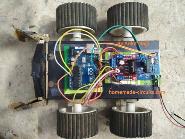
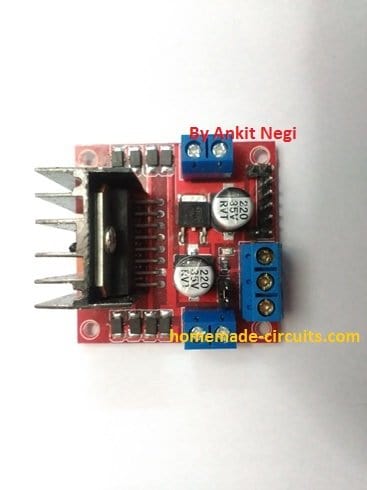 Arduino gives maximum current of 40mA using GPIO (general purpose input output) pins, while it gives 200mA using Vcc and ground.
Motors require large current to operate.
We canˇŻt use arduino directly to power our motors so we use a motor driver.
Motor driver contains H Bridge (which is a combination of transistors).
The IC (L298) of motor driver is driven by 5v which is supplied by arduino.
To power the motors, it takes 12v input from arduino which is ultimately supplied by a 12 v battery.
So the arduino just takes power from battery and gives to the motor driver.
It allows us to control the speed and direction of motors by giving maximum current of 2 amperes.
Arduino gives maximum current of 40mA using GPIO (general purpose input output) pins, while it gives 200mA using Vcc and ground.
Motors require large current to operate.
We canˇŻt use arduino directly to power our motors so we use a motor driver.
Motor driver contains H Bridge (which is a combination of transistors).
The IC (L298) of motor driver is driven by 5v which is supplied by arduino.
To power the motors, it takes 12v input from arduino which is ultimately supplied by a 12 v battery.
So the arduino just takes power from battery and gives to the motor driver.
It allows us to control the speed and direction of motors by giving maximum current of 2 amperes.
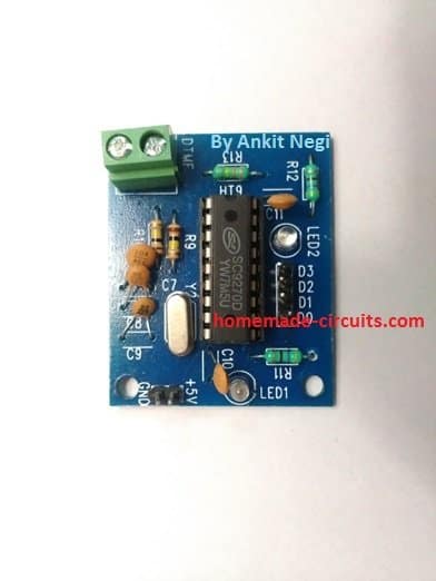 DTMF stands for Dual tone multi frequency.
Our dial pad is a two toner multiple frequency i.e.
one button gives a mixture of two tones having different frequency.
One tone is generated from a high frequency group of tones while other from a low frequency group.
It is done so that any type of voice canˇŻt imitate the tones.
So, it simply decodes the phone keypadˇŻs input into four bit binary code.
The frequencies of keypad numbers which we have used in our project is shown in the table below
DigitLow frequency(hertz)High frequency(hertz)2697133647701209677014778852133609411336
The binary decoded sequence of the dial padˇŻs digits is shown in the table below.
digitD3D2D1D010001200103001140100501016011070111810009100101010*1011#1100
CIRCUIT DIAGRAM
DTMF stands for Dual tone multi frequency.
Our dial pad is a two toner multiple frequency i.e.
one button gives a mixture of two tones having different frequency.
One tone is generated from a high frequency group of tones while other from a low frequency group.
It is done so that any type of voice canˇŻt imitate the tones.
So, it simply decodes the phone keypadˇŻs input into four bit binary code.
The frequencies of keypad numbers which we have used in our project is shown in the table below
DigitLow frequency(hertz)High frequency(hertz)2697133647701209677014778852133609411336
The binary decoded sequence of the dial padˇŻs digits is shown in the table below.
digitD3D2D1D010001200103001140100501016011070111810009100101010*1011#1100
CIRCUIT DIAGRAM
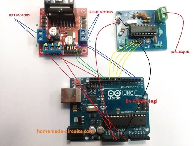
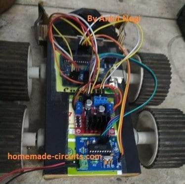
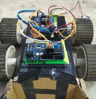
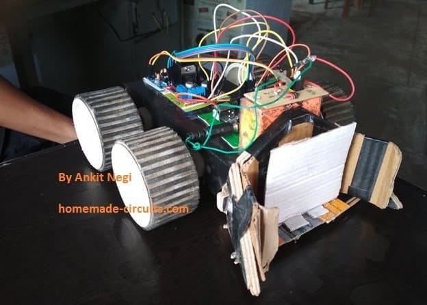
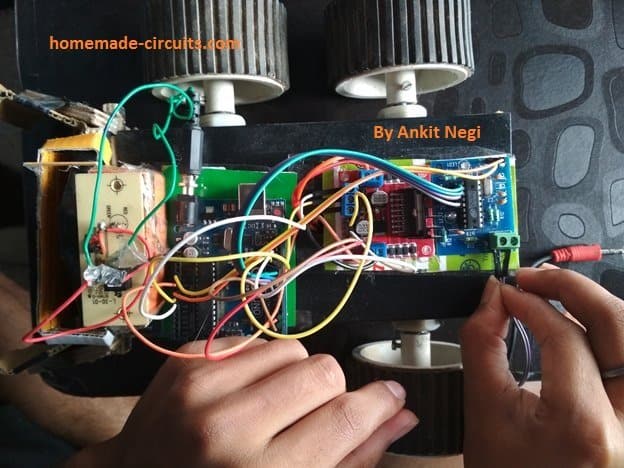

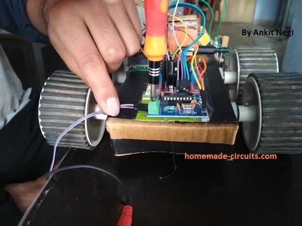
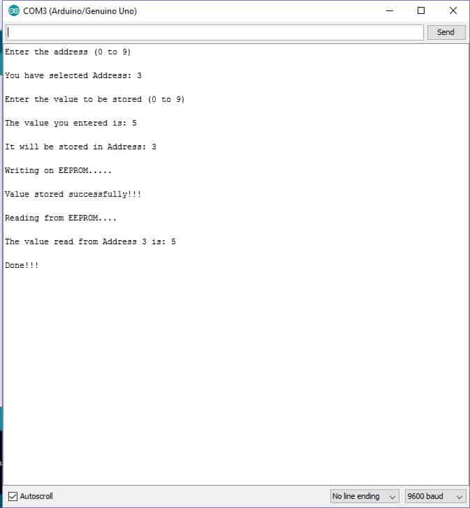 Once the code is uploaded, open the serial monitor.
It will ask you enter address ranging from 0 to 9. From the above output, I have entered address 3. So, I will be storing an integer value in the location (address) 3.
Now, it will prompt you to enter a single digit integer value ranging from 0 to 9. From the above output, I have entered value 5.
So, now the value 5 will be stored in the address location 3.
Once you enter the value, it will write the value on EEPROM.
It will show a success message, which means the value is stored.
After a couple of seconds it will read the value which is stored on the commented address and it will show the value on the serial monitor.
In conclusion, we have wrote and read the values from EEPROM of ArduinoˇŻs microcontroller.
Now, we are going to use the EEPROM for storing password.
We will be entering a 6 digit number (no less or no more) password, it will be stored in 6 different address (each address for each digit) and one additional address for storing ˇ°1ˇ± or ˇ°0ˇ±.
Once you enter the password, the additional address will store the value ˇ°1ˇ± indicating that password is set and the program will ask you to enter the password to turn ON the LED.
If the additional address stored value is ˇ°0ˇ± or any other value is present, it will ask you to create new 6 digit password.
By the above method, the program can identify whether you have already set a password or need to create a new password.
If the entered password is correct the build in LED at pin # 13 glows, if the entered password is incorrect, LED wonˇŻt glow and serial monitor will prompt that your password is wrong.
Once the code is uploaded, open the serial monitor.
It will ask you enter address ranging from 0 to 9. From the above output, I have entered address 3. So, I will be storing an integer value in the location (address) 3.
Now, it will prompt you to enter a single digit integer value ranging from 0 to 9. From the above output, I have entered value 5.
So, now the value 5 will be stored in the address location 3.
Once you enter the value, it will write the value on EEPROM.
It will show a success message, which means the value is stored.
After a couple of seconds it will read the value which is stored on the commented address and it will show the value on the serial monitor.
In conclusion, we have wrote and read the values from EEPROM of ArduinoˇŻs microcontroller.
Now, we are going to use the EEPROM for storing password.
We will be entering a 6 digit number (no less or no more) password, it will be stored in 6 different address (each address for each digit) and one additional address for storing ˇ°1ˇ± or ˇ°0ˇ±.
Once you enter the password, the additional address will store the value ˇ°1ˇ± indicating that password is set and the program will ask you to enter the password to turn ON the LED.
If the additional address stored value is ˇ°0ˇ± or any other value is present, it will ask you to create new 6 digit password.
By the above method, the program can identify whether you have already set a password or need to create a new password.
If the entered password is correct the build in LED at pin # 13 glows, if the entered password is incorrect, LED wonˇŻt glow and serial monitor will prompt that your password is wrong.
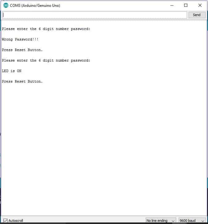 Open the serial monitor; it will prompt you to create a 6 digit number password.
Enter any 6 digit password and note it down and press enter.
Now the password has been stored.
You may either press the reset button or disconnect the USB cable from PC, which make the supply to Arduino board interrupted.
Now, reconnect the USB cable, open serial monitor, which will prompt you to enter the saved 6 digit password.
Enter the correct password the LED will glow.
If you want to change the password change the digit from the code:
int passExistAdd = 200;
The above line is the additional address which we discussed before.
Change anywhere from 6 to 1023. 0 to 5 addresses is reserved for storing 6 digit password.
Changing this additional address will fool the program that password is not created yet and prompt you to create a new 6 digit password.
If you have any questions regarding thisEEPROM in Arduino tutorial, please express in the comments, you may receive a quick reply.
Open the serial monitor; it will prompt you to create a 6 digit number password.
Enter any 6 digit password and note it down and press enter.
Now the password has been stored.
You may either press the reset button or disconnect the USB cable from PC, which make the supply to Arduino board interrupted.
Now, reconnect the USB cable, open serial monitor, which will prompt you to enter the saved 6 digit password.
Enter the correct password the LED will glow.
If you want to change the password change the digit from the code:
int passExistAdd = 200;
The above line is the additional address which we discussed before.
Change anywhere from 6 to 1023. 0 to 5 addresses is reserved for storing 6 digit password.
Changing this additional address will fool the program that password is not created yet and prompt you to create a new 6 digit password.
If you have any questions regarding thisEEPROM in Arduino tutorial, please express in the comments, you may receive a quick reply.

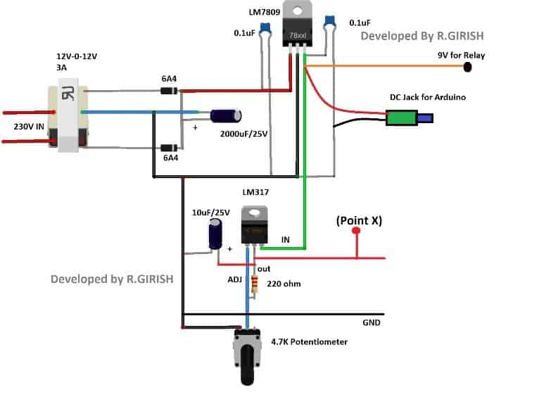 The 12v-0-12v / 3A transformer will be utilized for stepping down the voltage, the 6A4 diodes will convert the AC into DC voltage and the 2000uF capacitor will smooth out the choppy DC supply from diodes.
The LM 7809 fixed 9V regulator will convert the unregulated DC to regulated 9V DC supply.
The 9V supply will power the Arduino and relay.
Try to use a DC jack for arduinoˇŻs input supply.
DonˇŻt skip those 0.1uF ceramic capacitors which provide good stability for output voltage.
The LM 317 provides variable output voltage for the load which is to be connected.
You can adjust the output voltage by rotating the 4.7K ohm potentiometer.
That concludes the power section.
Now letˇŻs see the display connection:
The 12v-0-12v / 3A transformer will be utilized for stepping down the voltage, the 6A4 diodes will convert the AC into DC voltage and the 2000uF capacitor will smooth out the choppy DC supply from diodes.
The LM 7809 fixed 9V regulator will convert the unregulated DC to regulated 9V DC supply.
The 9V supply will power the Arduino and relay.
Try to use a DC jack for arduinoˇŻs input supply.
DonˇŻt skip those 0.1uF ceramic capacitors which provide good stability for output voltage.
The LM 317 provides variable output voltage for the load which is to be connected.
You can adjust the output voltage by rotating the 4.7K ohm potentiometer.
That concludes the power section.
Now letˇŻs see the display connection:

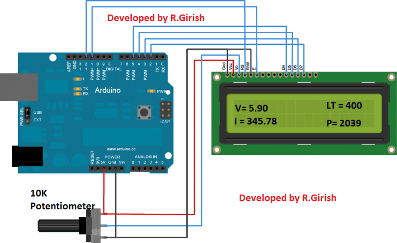 There is nothing to explain here much, just wire up the Arduino and LCD display as per the circuit diagram.
Adjust the 10K potentiometer for better viewing contrast.
The above display shows the sample readings for the four parameters mentioned.
There is nothing to explain here much, just wire up the Arduino and LCD display as per the circuit diagram.
Adjust the 10K potentiometer for better viewing contrast.
The above display shows the sample readings for the four parameters mentioned.

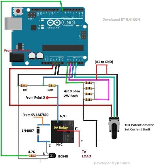 Relay Connection Details for the above Design:

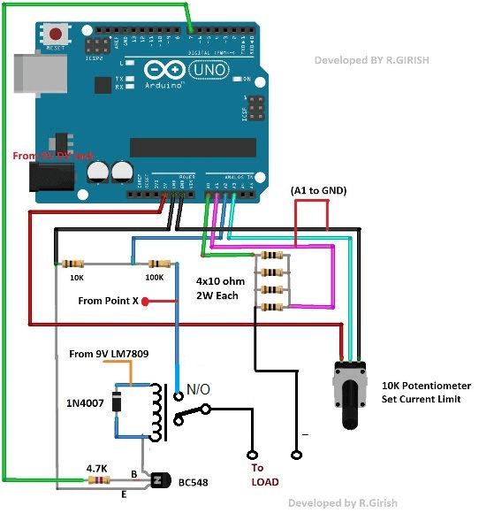 The four 10 ohm resistors in parallel which forms 2.5 ohm shunt resistor which will be utilized for measuring the current flow through the load.
The resistors should be at least 2 watt each.
The 10k ohm and 100k ohm resistors helps the Arduino to measure voltage at the load.
These resistor can be one with normal wattage rating.
If you want to know more about the working of Arduino based ammeter and voltmeter check out these two links:
Voltmeter: https://www.homemade-circuits.com/2016/09/how-to-make-dc-voltmeter-using-arduino.html
Ammeter: https://www.homemade-circuits.com/2017/08/arduino-dc-digital-ammeter.html
The 10K ohm potentiometer is provided for adjusting the maximum current level at the output.
If the current flow through the load exceeds the pre-set current the output supply will be disconnected.
You can see the preset level in the display it will be mentioned as ˇ°LTˇ± (Limit).
Say for example: if you set the limit as 200, it will gives out current till 199mA.
If the current consumption gets equal to 200 mA or above the output will be immediately cut-off.
The output is turned on and off by the Arduino pin #7. When this pin is high the transistor energizes the relay which connects the common and normally open pins, which conducts the positive supply for the load.
The diode IN4007 absorbs the high voltage back EMF from the relay coil while switching the relay ON and OFF.
The four 10 ohm resistors in parallel which forms 2.5 ohm shunt resistor which will be utilized for measuring the current flow through the load.
The resistors should be at least 2 watt each.
The 10k ohm and 100k ohm resistors helps the Arduino to measure voltage at the load.
These resistor can be one with normal wattage rating.
If you want to know more about the working of Arduino based ammeter and voltmeter check out these two links:
Voltmeter: https://www.homemade-circuits.com/2016/09/how-to-make-dc-voltmeter-using-arduino.html
Ammeter: https://www.homemade-circuits.com/2017/08/arduino-dc-digital-ammeter.html
The 10K ohm potentiometer is provided for adjusting the maximum current level at the output.
If the current flow through the load exceeds the pre-set current the output supply will be disconnected.
You can see the preset level in the display it will be mentioned as ˇ°LTˇ± (Limit).
Say for example: if you set the limit as 200, it will gives out current till 199mA.
If the current consumption gets equal to 200 mA or above the output will be immediately cut-off.
The output is turned on and off by the Arduino pin #7. When this pin is high the transistor energizes the relay which connects the common and normally open pins, which conducts the positive supply for the load.
The diode IN4007 absorbs the high voltage back EMF from the relay coil while switching the relay ON and OFF.
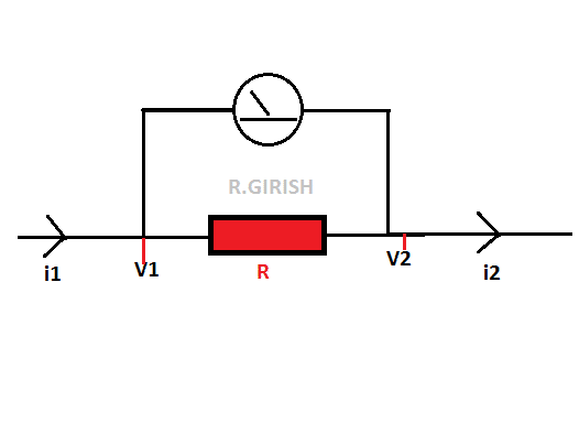 A shunt resistor with very low resistance R and assume some kind analog meter is connected across the resistor whoˇŻs deflection is directly proportional to voltage through the analog meter.
Now letˇŻs pass some amount of current from left hand side.
i1 is the current before entering the shunt resistor R and i2 will be the current after passing through shunt resistor.
The current i1 will be greater than i2 since it dropped a fraction of current through shunt resistor.
The current difference between the shunt resistor develops very small amount of voltage at V1 and V2.
The amount of voltage will be measured by that analog meter.
The voltage developed across the shunt resistor depends on two factors: the current flowing through the shunt resistor and the value of the shunt resistor.
If the current flow is greater through the shunt the voltage developed is more.
If the value of the shunt is high the voltage developed across the shunt is more.
The shunt resistor must be very tiny value and it must possess higher wattage rating.
A small value resistor ensures that the load is getting adequate amount of current and voltage for normal operation.
Also the shunt resistor must have higher wattage rating so that it can tolerate the higher temperature while measuring the current.
Higher the current through the shunt more the heat is generated.
By now you would have got the basic idea, how an analog meter works.
Now letˇŻs move on to digital design.
By now we know that a resistor will produce a voltage if there is a current flow.
From the diagram V1 and V2 are the points, where we take the voltage samples to the microcontroller.
A shunt resistor with very low resistance R and assume some kind analog meter is connected across the resistor whoˇŻs deflection is directly proportional to voltage through the analog meter.
Now letˇŻs pass some amount of current from left hand side.
i1 is the current before entering the shunt resistor R and i2 will be the current after passing through shunt resistor.
The current i1 will be greater than i2 since it dropped a fraction of current through shunt resistor.
The current difference between the shunt resistor develops very small amount of voltage at V1 and V2.
The amount of voltage will be measured by that analog meter.
The voltage developed across the shunt resistor depends on two factors: the current flowing through the shunt resistor and the value of the shunt resistor.
If the current flow is greater through the shunt the voltage developed is more.
If the value of the shunt is high the voltage developed across the shunt is more.
The shunt resistor must be very tiny value and it must possess higher wattage rating.
A small value resistor ensures that the load is getting adequate amount of current and voltage for normal operation.
Also the shunt resistor must have higher wattage rating so that it can tolerate the higher temperature while measuring the current.
Higher the current through the shunt more the heat is generated.
By now you would have got the basic idea, how an analog meter works.
Now letˇŻs move on to digital design.
By now we know that a resistor will produce a voltage if there is a current flow.
From the diagram V1 and V2 are the points, where we take the voltage samples to the microcontroller.
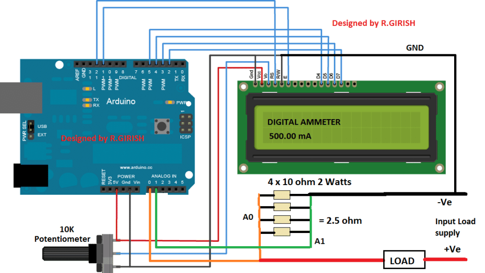 The proposed circuit is very simple and beginner friendly.
Construct as per the circuit diagram.
Adjust the 10K potentiometer to adjust display contrast.
You can power the Arduino from USB or via DC jack with 9 V batteries.
Four 2 watt resistors will dissipate the heat evenly than using one 2.5 ohm resistor with 8- 10 watt resistor.
When no current is passing the display may read some small random value which you may ignore it, this might be due to stray voltage across measuring terminals.
NOTE: DonˇŻt reverse the input load supply polarity.
The proposed circuit is very simple and beginner friendly.
Construct as per the circuit diagram.
Adjust the 10K potentiometer to adjust display contrast.
You can power the Arduino from USB or via DC jack with 9 V batteries.
Four 2 watt resistors will dissipate the heat evenly than using one 2.5 ohm resistor with 8- 10 watt resistor.
When no current is passing the display may read some small random value which you may ignore it, this might be due to stray voltage across measuring terminals.
NOTE: DonˇŻt reverse the input load supply polarity.
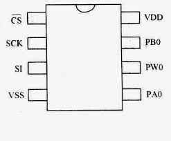 FIG.
MC41010 IC pinout
MC41010 is an 8 pin dual in line package IC.
Just like any analog potentiometer this IC comes in 5k, 10k, 50k, and 100k.
In this circuit 10k potentiometer is used
MC4131 have following 8 terminals:
FIG.
MC41010 IC pinout
MC41010 is an 8 pin dual in line package IC.
Just like any analog potentiometer this IC comes in 5k, 10k, 50k, and 100k.
In this circuit 10k potentiometer is used
MC4131 have following 8 terminals:
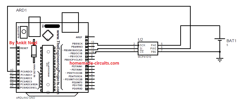
 These are some simulation pictures for this circuit at various values of i:
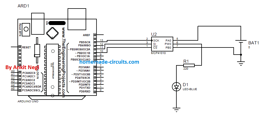 Now just connect an led in series with 220ohm resistor to wiper terminal of IC as shown in figure.
 Simulation3
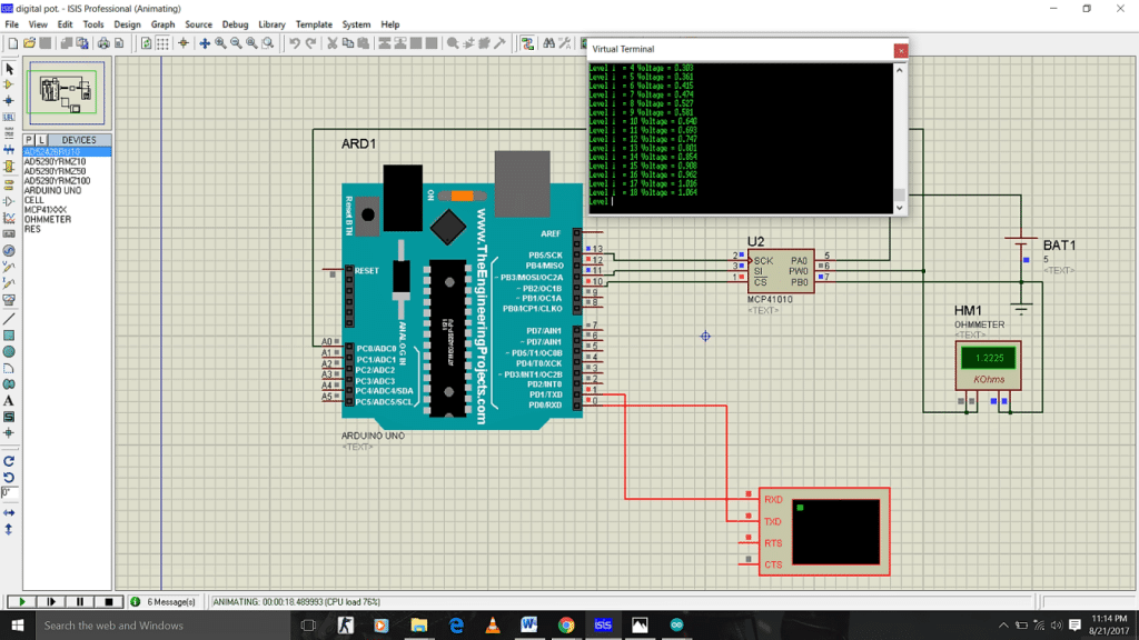
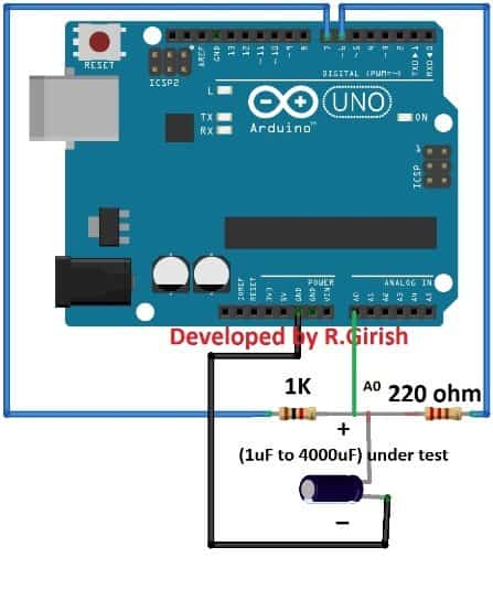 As you can see the circuit is very simple just a couple of resistors are needed to find the unknown capacitance.The 1K ohm is the known resistor value and the 220 ohm resistor utilized for discharging the capacitor while measurement process takes place.The Arduino sense the rising and decreasing voltage on pin A0 which is connected between 1K ohm and 220 ohm resistors.Please take care of the polarity if you are using polarized capacitors such as electrolytic.Program:
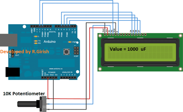
 The above circuit is exactly same as serial monitor based design; you just need to connect LCD display.
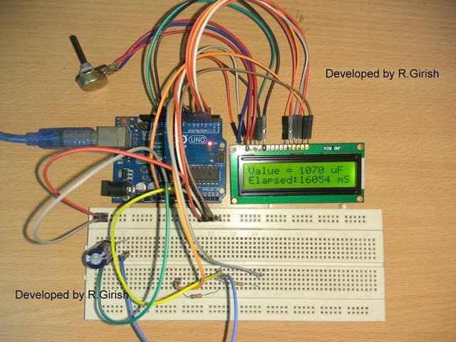
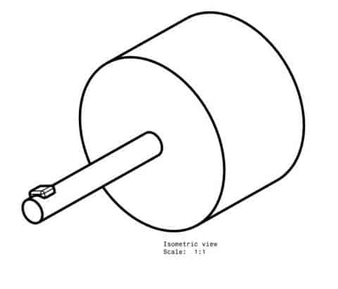
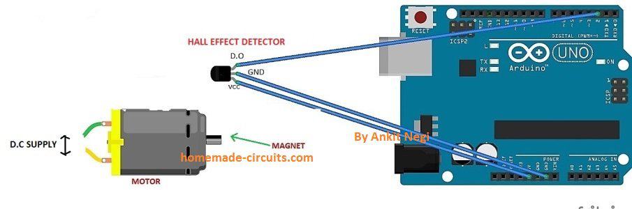 Now Interrupt can be called at certain condition defined by the user using an inbuilt Arduino Syntax.We will be using this Interrupt in our project that makes our tachometer more resolute as well as more precise than the other Tachometer project present around the web.
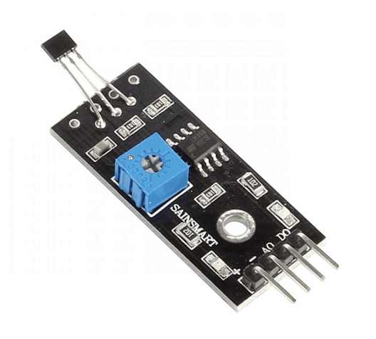 Arduino Uno
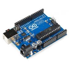 Small magnet
 Jumper wires
Rotating Object (Motor shaft)
Jumper wires
Rotating Object (Motor shaft)
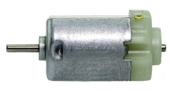
 3. 1k ohm resistor (2 watt)
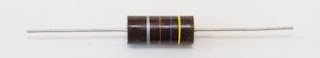 4. 1N4007 diode
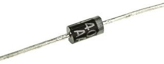 5. One zener diode 5 volts
 6. 1 uf capacitor
 7. Connecting wires
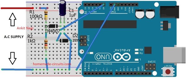 Make connections as shown in circuit diagram.
A) Make a voltage divider using resistors keeping in mind that 1 k ohm resistor should be connected to ground.
B) Connect diodeˇŻs p- terminal directly after 1 k ohm resistor as shown in fig.
and its n- terminal to 1 uf capacitor.
C) DonˇŻt forget to connect zener diode in parallel to the capacitor( explained below)
D) Connect a wire from positive terminal of capacitor to the analog pin A0 of arduino.
E) ** do connect the ground pin of arduino to the overall ground else circuit will not work.
Make connections as shown in circuit diagram.
A) Make a voltage divider using resistors keeping in mind that 1 k ohm resistor should be connected to ground.
B) Connect diodeˇŻs p- terminal directly after 1 k ohm resistor as shown in fig.
and its n- terminal to 1 uf capacitor.
C) DonˇŻt forget to connect zener diode in parallel to the capacitor( explained below)
D) Connect a wire from positive terminal of capacitor to the analog pin A0 of arduino.
E) ** do connect the ground pin of arduino to the overall ground else circuit will not work.
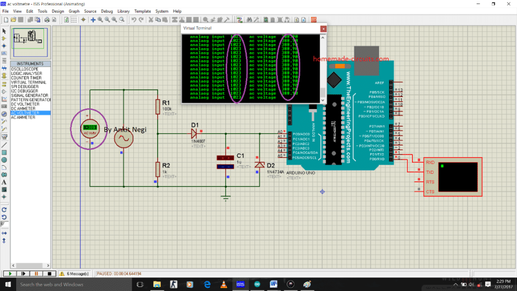 In r.m.s 550 peak volts = 550/1.414= 388.96 volts r.m.s.
Hence for this r.m.s value we obtain 5 volts on pin A0. So this circuit can measure maximum of 389 volts.
Now for 1023 analog value on pin A0 --- 389 a.c volts = y
Which gives, for any analog value(x); y = (389/1023)*x a.c volts
OR y =.38015*x a.c volts
You can clearly observe in fig that printed a.c value on serial monitor is also 389 volts
Printing required values on screen::
We require two values to be printed on serial monitor as shown in the simulation picture:
1. Analog input value received by analog pin A0 as specified in the code:
Serial.print(" analaog input ") ; // specify name to the corresponding value to be printed
Serial.print(x) ; // print input analog value on serial monitor
2. Actual value of ac voltage from mains as specified in the code:
Serial.print(" ac voltage ") ; // specify name to the corresponding value to be printed
Serial.print(y) ; // prints the ac value on Serial monitor
In r.m.s 550 peak volts = 550/1.414= 388.96 volts r.m.s.
Hence for this r.m.s value we obtain 5 volts on pin A0. So this circuit can measure maximum of 389 volts.
Now for 1023 analog value on pin A0 --- 389 a.c volts = y
Which gives, for any analog value(x); y = (389/1023)*x a.c volts
OR y =.38015*x a.c volts
You can clearly observe in fig that printed a.c value on serial monitor is also 389 volts
Printing required values on screen::
We require two values to be printed on serial monitor as shown in the simulation picture:
1. Analog input value received by analog pin A0 as specified in the code:
Serial.print(" analaog input ") ; // specify name to the corresponding value to be printed
Serial.print(x) ; // print input analog value on serial monitor
2. Actual value of ac voltage from mains as specified in the code:
Serial.print(" ac voltage ") ; // specify name to the corresponding value to be printed
Serial.print(y) ; // prints the ac value on Serial monitor
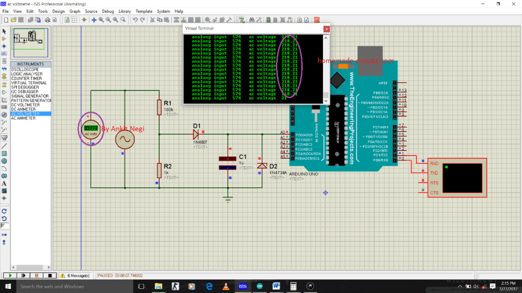 B) 235 volts or 332.9 amplitude
 C) 300 volts or 424.2
 Hence from the following results it is observed that for 220 a.c supply, arduino shows 217 volts.
And as this a.c value increases, results of simulation become more accurate that is more close to the input a.c value.
Hence from the following results it is observed that for 220 a.c supply, arduino shows 217 volts.
And as this a.c value increases, results of simulation become more accurate that is more close to the input a.c value.
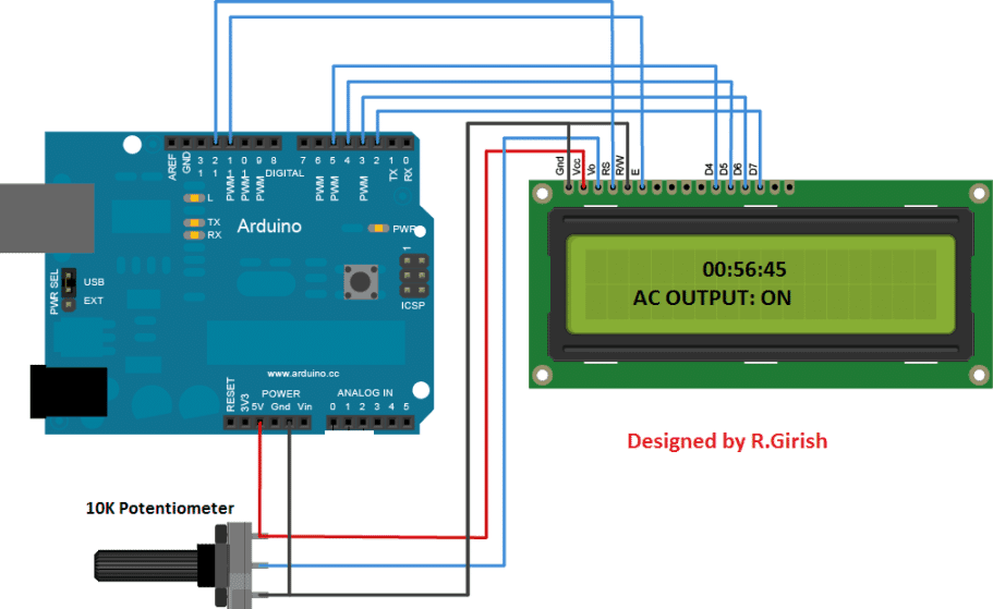 The above circuit is the arduino to LCD display connection, a 10K potentiometer is provided for adjusting the contrast of the display.
Rest of the above connections are self-explanatory.
The above circuit is the arduino to LCD display connection, a 10K potentiometer is provided for adjusting the contrast of the display.
Rest of the above connections are self-explanatory.
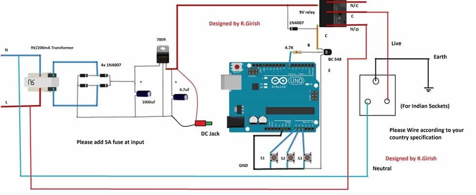 The circuit needs power to operate so, a simple regulated power supply is provided; it can output constant 9V to arduino and relay.
S1, S2 and S3 are push buttons by which the user can set time.
S1 is hour button S2 is minute button and S3 is start button.
A 1N4007 diode is connected across the relay terminal to absorb high voltage back EMF from the relay while switching.
Use at-least 5A relay and 5A output socket.
Connect a 5A fuse at the input supply.
Always use 3-pin plug at input; donˇŻt skip earth wiring and donˇŻt interchange Live and Neutral lines.
The circuit needs power to operate so, a simple regulated power supply is provided; it can output constant 9V to arduino and relay.
S1, S2 and S3 are push buttons by which the user can set time.
S1 is hour button S2 is minute button and S3 is start button.
A 1N4007 diode is connected across the relay terminal to absorb high voltage back EMF from the relay while switching.
Use at-least 5A relay and 5A output socket.
Connect a 5A fuse at the input supply.
Always use 3-pin plug at input; donˇŻt skip earth wiring and donˇŻt interchange Live and Neutral lines.
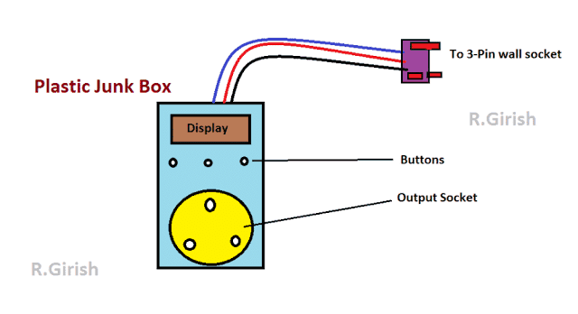
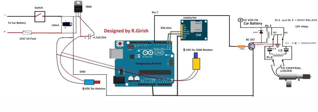 The above circuit is fairly easy to replicate one.
The GSM modem is interfaced with ArduinoˇŻs Tx and Rx pin.
The Tx of Arduino is connected to Rx of GSM modem and Rx of Arduino is connected Tx of GSM modem i.e.
Tx to Rx and Rx to Tx.
Ground to ground connection between Arduino and GSM modem is also established.
A 9V regulator 7809 is added in the circuit to provide to fixed voltage to GSM modem and arduino board as the battery voltage is subjected to change while ignition and charging, higher than 12 volt may damage the boards.
The ArduinoˇŻs PIN # 7 is the output to the central lock and ignition lock mechanism.
The above circuit is fairly easy to replicate one.
The GSM modem is interfaced with ArduinoˇŻs Tx and Rx pin.
The Tx of Arduino is connected to Rx of GSM modem and Rx of Arduino is connected Tx of GSM modem i.e.
Tx to Rx and Rx to Tx.
Ground to ground connection between Arduino and GSM modem is also established.
A 9V regulator 7809 is added in the circuit to provide to fixed voltage to GSM modem and arduino board as the battery voltage is subjected to change while ignition and charging, higher than 12 volt may damage the boards.
The ArduinoˇŻs PIN # 7 is the output to the central lock and ignition lock mechanism.
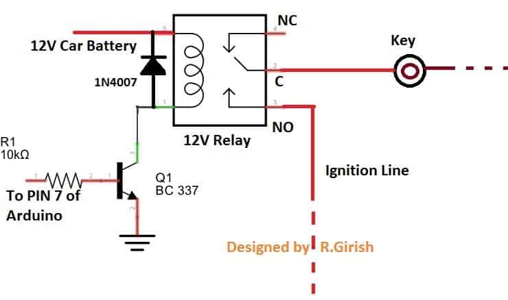 The diodes are connected to prevent high voltage spike from relay due to back EMF.
A fuse must be connected at the input as the short circuit can turn into catastrophic damage to the car.
A switch is provided which may be placed inside the bonnet.
It can used to turn off the circuit if you are not planning to use the car for more than a week which will avoid battery drain.
NOTE: If the circuit is turned off (using switch) the central and ignition lock is activated and your car is safe.
The diodes are connected to prevent high voltage spike from relay due to back EMF.
A fuse must be connected at the input as the short circuit can turn into catastrophic damage to the car.
A switch is provided which may be placed inside the bonnet.
It can used to turn off the circuit if you are not planning to use the car for more than a week which will avoid battery drain.
NOTE: If the circuit is turned off (using switch) the central and ignition lock is activated and your car is safe.
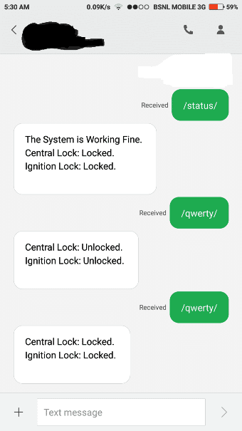


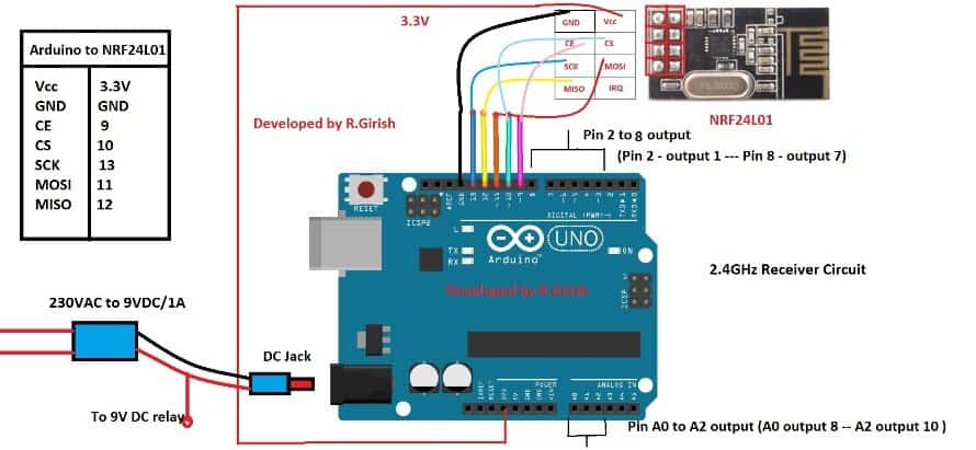 If you are confused with wiring diagram between Arduino and NRF24L01 module, just take a look at the table beside the schematic, it is same for remote controller circuit too.
The output sequence and output pins are as follows:
Arduino PIN ¨C Output sequence
PIN 2 ¨C OUTPUT 1
PIN 3 ¨C OUTPUT 2
PIN 4 ¨C OUTPUT 3
PIN 5 ¨C OUTPUT 4
PIN 6 ¨C OUTPUT 5
PIN 7 ¨C OUTPUT 6
PIN 8 ¨C OUTPUT 7
PIN A0 ¨C OUTPUT 8
PIN A1 ¨C OUTPUT 9
PIN A2 ¨C OUTPUT 10
If you are confused with wiring diagram between Arduino and NRF24L01 module, just take a look at the table beside the schematic, it is same for remote controller circuit too.
The output sequence and output pins are as follows:
Arduino PIN ¨C Output sequence
PIN 2 ¨C OUTPUT 1
PIN 3 ¨C OUTPUT 2
PIN 4 ¨C OUTPUT 3
PIN 5 ¨C OUTPUT 4
PIN 6 ¨C OUTPUT 5
PIN 7 ¨C OUTPUT 6
PIN 8 ¨C OUTPUT 7
PIN A0 ¨C OUTPUT 8
PIN A1 ¨C OUTPUT 9
PIN A2 ¨C OUTPUT 10
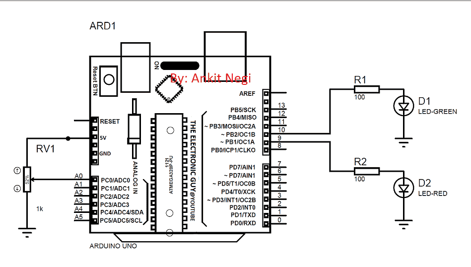
 4. BATTERY (12v) : to supply power to motor.
5. TWO PUSHBUTTONS: to give inputs to arduino (i.e.
when pressed and when not pressed)
4. BATTERY (12v) : to supply power to motor.
5. TWO PUSHBUTTONS: to give inputs to arduino (i.e.
when pressed and when not pressed)
 6. TWO 10K RESISTORS: for debouncing (explained below)
 7. CONNECTING WIRES: for making connections.
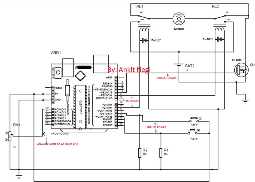 Make connections as shown in the figure.
1. Connect normally open terminal of both relay to positive terminal of battery and normally closed terminal to batteryˇŻs negative terminal.
2. Connect the motor in between the remaining terminal (out of three) of each relay.
3. Connect one terminal of primary side of relays to the output pins of arduino as specified in the code and other terminal to ground.
4. Connect one terminal of both pushbuttons to 5v pin of arduino and other terminal to input pins as specified in the code.
4. **DonˇŻt forget to connect resistors as they are very important for proper functioning of this circuit, as explained below:
WHY RESISTORS ARE CONNECTED?
You may find that there's nothing at all connected to input pins of Arduino, but that does not mean these pinouts may be a logical zero when the indicated switch is open
Rather it implies that when switch is open arduino can take any random value between logic 0 and logic 1, which is not good at all (this is called bouncing).
So what we want here is that when nothing is connected to the input pin i.e.
pushbutton is open, arduino takes 0 input from the pin.
And to achieve this, the pin is directly connected to ground before the pushbutton via resistor.
If it is directly connected to ground without resistor there are good chances that it will burn out as pin will be shorted to ground and huge amount of current will flow.
To prevent this, a resistor is connected in between.
This resistor is called pulldown resistor as it is pulling logic on pin to 0. And this process is called debouncing.
CODE:
Burn this code into your arduino.
Make connections as shown in the figure.
1. Connect normally open terminal of both relay to positive terminal of battery and normally closed terminal to batteryˇŻs negative terminal.
2. Connect the motor in between the remaining terminal (out of three) of each relay.
3. Connect one terminal of primary side of relays to the output pins of arduino as specified in the code and other terminal to ground.
4. Connect one terminal of both pushbuttons to 5v pin of arduino and other terminal to input pins as specified in the code.
4. **DonˇŻt forget to connect resistors as they are very important for proper functioning of this circuit, as explained below:
WHY RESISTORS ARE CONNECTED?
You may find that there's nothing at all connected to input pins of Arduino, but that does not mean these pinouts may be a logical zero when the indicated switch is open
Rather it implies that when switch is open arduino can take any random value between logic 0 and logic 1, which is not good at all (this is called bouncing).
So what we want here is that when nothing is connected to the input pin i.e.
pushbutton is open, arduino takes 0 input from the pin.
And to achieve this, the pin is directly connected to ground before the pushbutton via resistor.
If it is directly connected to ground without resistor there are good chances that it will burn out as pin will be shorted to ground and huge amount of current will flow.
To prevent this, a resistor is connected in between.
This resistor is called pulldown resistor as it is pulling logic on pin to 0. And this process is called debouncing.
CODE:
Burn this code into your arduino.
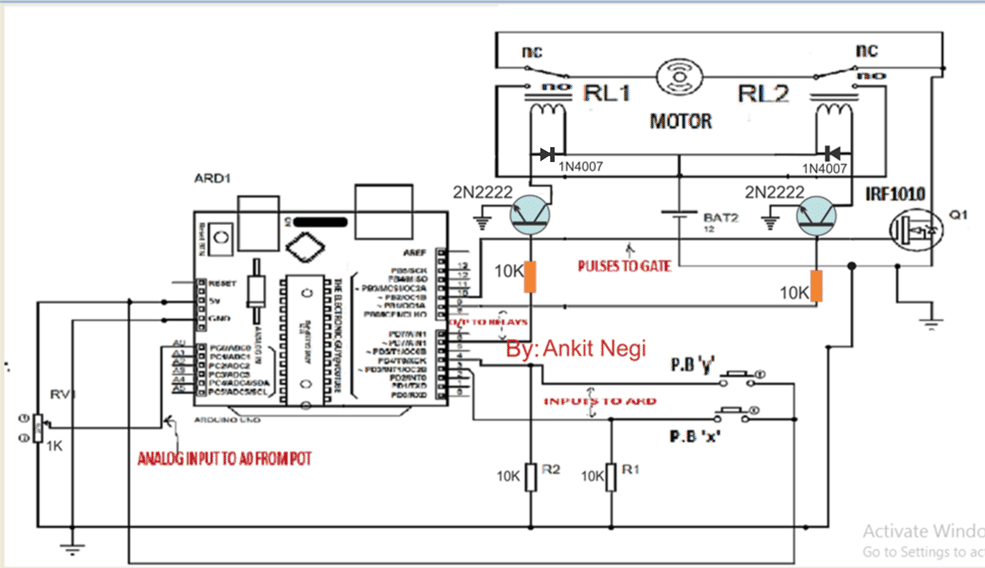
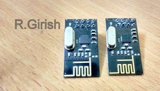 This module is designed to establish bi-directional communication link between two microcontrollers.
It works on SPI communication protocol.
It has 125 different channels and has maximum data rate of 2Mbps.
It has theoretical maximum range of 100 meter.
This module is designed to establish bi-directional communication link between two microcontrollers.
It works on SPI communication protocol.
It has 125 different channels and has maximum data rate of 2Mbps.
It has theoretical maximum range of 100 meter.
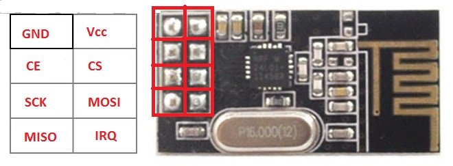 It operates on 3.3V, so 5 volt on Vcc terminal can kill it.
However, it can accept 5V data signals from microcontrollers.
Now letˇŻs move on to the transmitter of the project.
It operates on 3.3V, so 5 volt on Vcc terminal can kill it.
However, it can accept 5V data signals from microcontrollers.
Now letˇŻs move on to the transmitter of the project.
 Adjust the 10K potentiometer for better viewing contrast.
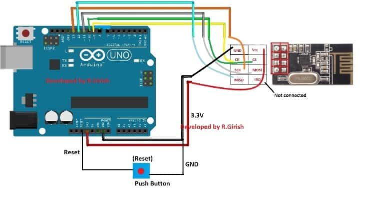 The above schematic is rest of the receiver circuit.
A push button is provided for resetting the arduino in case of the 2.4 GHz link connection is not established.
The above schematic is rest of the receiver circuit.
A push button is provided for resetting the arduino in case of the 2.4 GHz link connection is not established.
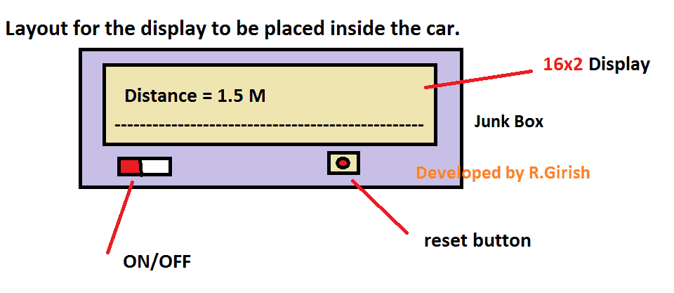 The receiver circuit is placed inside the car; it can be power from a 9V battery.
The receiver may be placed in a junk box which might make your car look good.
The junk box may be placed in your car above the instrument cluster or any convenient place you wish.
The receiver circuit is placed inside the car; it can be power from a 9V battery.
The receiver may be placed in a junk box which might make your car look good.
The junk box may be placed in your car above the instrument cluster or any convenient place you wish.
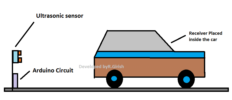
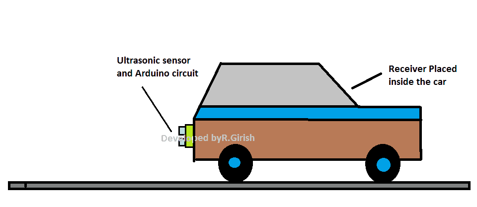
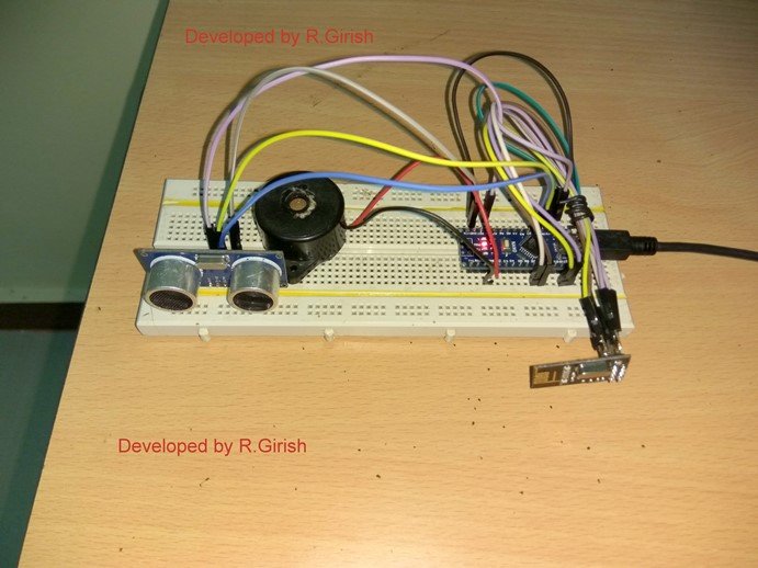
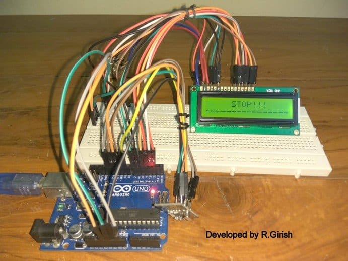
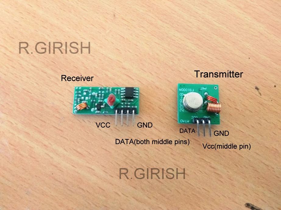 The transmitter and receiver modules are shown above; it is capable of simplex communication (one way).
The receiver has 4 pins Vcc, GND and DATA pins.
There are two DATA pins, they are same and we can output the data from either of two pins.
The transmitter is much simpler it has just Vcc, GND and DATA input pin.
We have to connect an antenna to both modules which is described at the end of the article, without antenna communication between them wonˇŻt be established beyond few inches.
Now letˇŻs see how these modules communicate.
Now assume we are applying clock pulse of 100Hz to the transmitterˇŻs data input pin.
The receiver will receive exact replica of the signal at receiverˇŻs data pin.
ThatˇŻs simple right? Yeahˇ but this module works on AM and susceptible to noise.
From authorˇŻs observation if the transmitterˇŻs data pin left without any signal for more than 250 milliseconds, the receiver data output pin produce random signals.
So, it is only suitable for non-critical data transmissions.
However this project works very well with this module.
Now letˇŻs move on to schematics.
The transmitter and receiver modules are shown above; it is capable of simplex communication (one way).
The receiver has 4 pins Vcc, GND and DATA pins.
There are two DATA pins, they are same and we can output the data from either of two pins.
The transmitter is much simpler it has just Vcc, GND and DATA input pin.
We have to connect an antenna to both modules which is described at the end of the article, without antenna communication between them wonˇŻt be established beyond few inches.
Now letˇŻs see how these modules communicate.
Now assume we are applying clock pulse of 100Hz to the transmitterˇŻs data input pin.
The receiver will receive exact replica of the signal at receiverˇŻs data pin.
ThatˇŻs simple right? Yeahˇ but this module works on AM and susceptible to noise.
From authorˇŻs observation if the transmitterˇŻs data pin left without any signal for more than 250 milliseconds, the receiver data output pin produce random signals.
So, it is only suitable for non-critical data transmissions.
However this project works very well with this module.
Now letˇŻs move on to schematics.
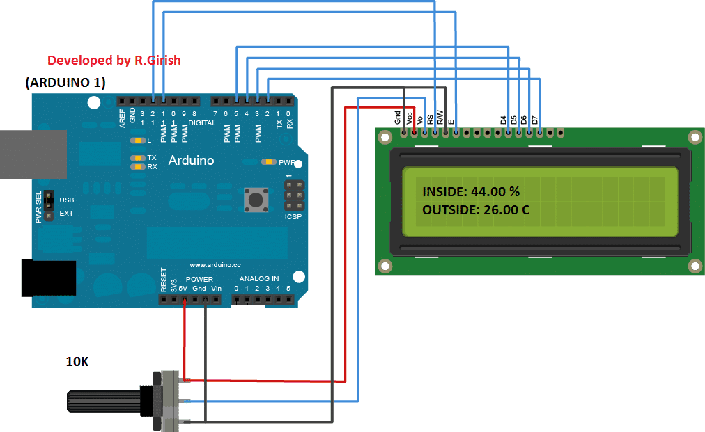 The above circuit is arduino to LCD display connection.
10K potentiometer is provided for adjusting contrast of LCD display.
The above circuit is arduino to LCD display connection.
10K potentiometer is provided for adjusting contrast of LCD display.
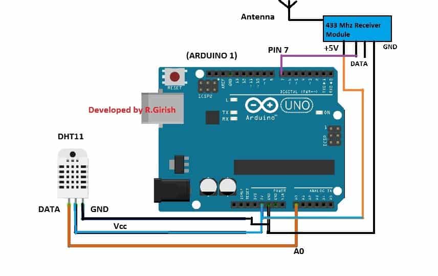 The above is the receiver circuit.
The LCD display should be connected to this arduino.
Please download the following library files before compiling the code
Radio Head : github.com/PaulStoffregen/RadioHead
DHT sensor library : https://arduino-info.wikispaces.com/file/detail/DHT-lib.zip
The above is the receiver circuit.
The LCD display should be connected to this arduino.
Please download the following library files before compiling the code
Radio Head : github.com/PaulStoffregen/RadioHead
DHT sensor library : https://arduino-info.wikispaces.com/file/detail/DHT-lib.zip
 Use a single core wire which should be sturdy enough to support this structure.
You can also use insulated copper wire with insulation removed at bottom for solder join.
Make two of these, one for transmitter and another for receiver.
Use a single core wire which should be sturdy enough to support this structure.
You can also use insulated copper wire with insulation removed at bottom for solder join.
Make two of these, one for transmitter and another for receiver.
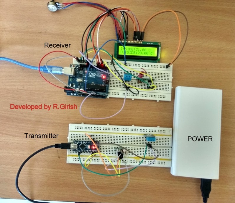
 The proposed EVM circuit can only accommodate 6 candidates.
A control button is provided similar to control unit in real EVMs.
After a person caste his/her vote, the ballot buttons are disabled.
The ballot buttons are enabled again only after pressing the control button.
The control button will be placed near the person in charge who controls the election booth.
After a person cast a vote he/she is acknowledged with activation of LED and buzzer.
The person can also confirm the vote to whom he/she casted in the display, it will show the candidate name or the party name for couple of seconds.
This feature is not still present in real EVMs.
Schematic Diagram:
The proposed EVM circuit can only accommodate 6 candidates.
A control button is provided similar to control unit in real EVMs.
After a person caste his/her vote, the ballot buttons are disabled.
The ballot buttons are enabled again only after pressing the control button.
The control button will be placed near the person in charge who controls the election booth.
After a person cast a vote he/she is acknowledged with activation of LED and buzzer.
The person can also confirm the vote to whom he/she casted in the display, it will show the candidate name or the party name for couple of seconds.
This feature is not still present in real EVMs.
Schematic Diagram:
 The circuit is divided into two parts to avoid confusions while duplicating the project.
The above circuit describes the wiring between LCD display and arduino.
Adjust the variable resistor for optimum contrast.
The circuit is divided into two parts to avoid confusions while duplicating the project.
The above circuit describes the wiring between LCD display and arduino.
Adjust the variable resistor for optimum contrast.
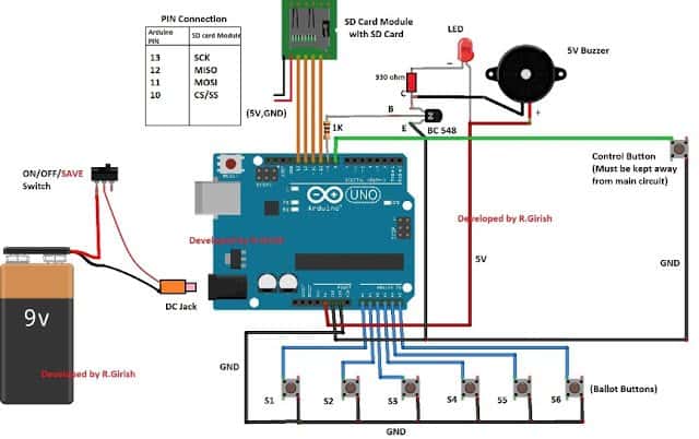 Here is the rest of the circuit consisting of 9V battery, switch, seven push buttons, LED, buzzer and more importantly SD card module.
The SD card will store the data instantly after a vote is casted.
Once the election is over; the SD card is inserted to a computer to declare the vote count and result.
The Proposed design can record up to 4,294,967,295 (which is more than 4 billion) votes per candidate and 25,769,803,770 (more than 25 billion which is more than thrice the current worldˇŻs population) votes per machine and still more than 99.9% SD card is still empty.
This is far more efficient than real EVMs which can record 3840 votes per machine.
Here is the rest of the circuit consisting of 9V battery, switch, seven push buttons, LED, buzzer and more importantly SD card module.
The SD card will store the data instantly after a vote is casted.
Once the election is over; the SD card is inserted to a computer to declare the vote count and result.
The Proposed design can record up to 4,294,967,295 (which is more than 4 billion) votes per candidate and 25,769,803,770 (more than 25 billion which is more than thrice the current worldˇŻs population) votes per machine and still more than 99.9% SD card is still empty.
This is far more efficient than real EVMs which can record 3840 votes per machine.

 Opening a file will show the name of the candidate and number of vote, as illustrated below:

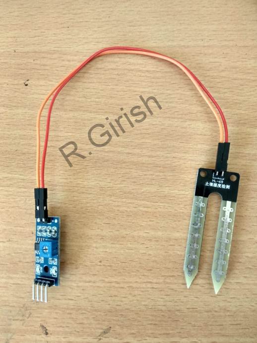 It has 4 + 2 pins, 2 pins for electrode connection and rest of the 4 pins are Vcc, GND, digital output and analog output.
We are going to use only the analog output pin for sensing soil moisture.
Since we are not using digital output pin, we will not be using on-board trimmer resistor to calibrate the sensor.
Now, that concludes the soil moisture sensor.
It has 4 + 2 pins, 2 pins for electrode connection and rest of the 4 pins are Vcc, GND, digital output and analog output.
We are going to use only the analog output pin for sensing soil moisture.
Since we are not using digital output pin, we will not be using on-board trimmer resistor to calibrate the sensor.
Now, that concludes the soil moisture sensor.
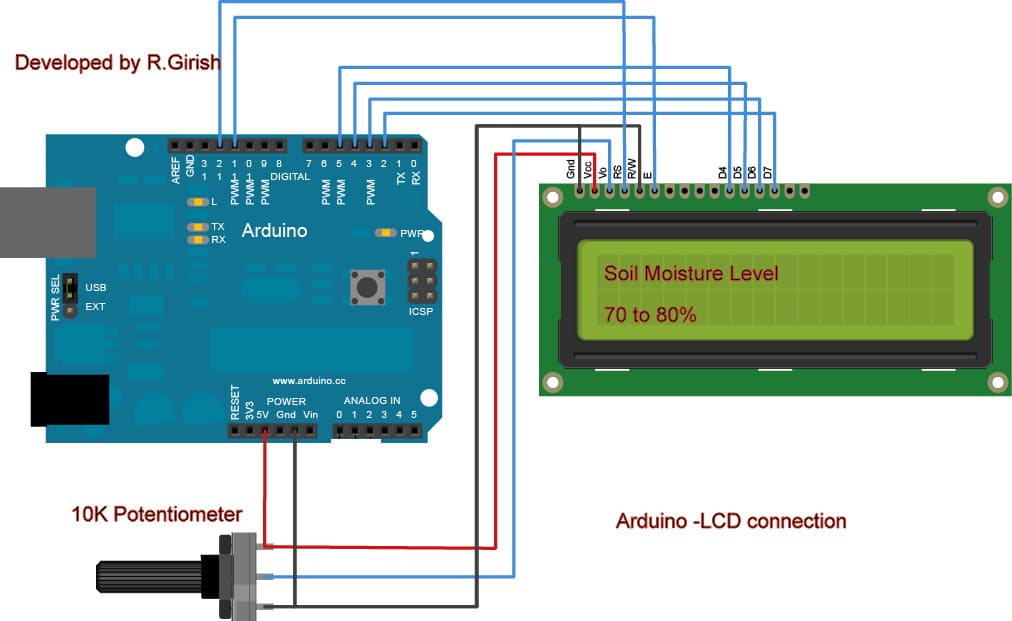 The above schematic is the LCD to arduino wiring.
A 10K potentiometer is provided to adjust the contrast of the LCD display.
The above schematic is the LCD to arduino wiring.
A 10K potentiometer is provided to adjust the contrast of the LCD display.
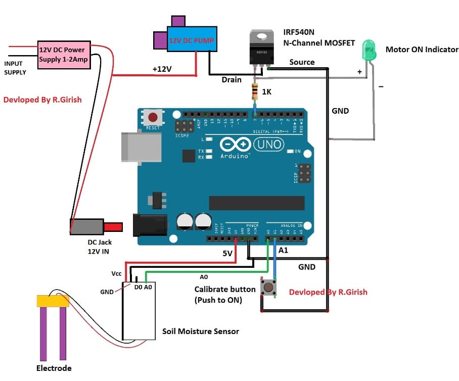 Here is the rest of the schematic consisting of soil moisture sensor, 12V DC pump, a calibrate push button and 12V (1 - 2 amp) power supply.
Please use a power supply at least greater than 500mA of 12V DC pumpˇŻs current rating.
The MOSFET IRF540N (or any equivalent N-channel) is used instead of BJTs to improve the overall power efficiency of the system.
The pump will water you small garden, make sure you always have adequate amount of water is available.
Here is the rest of the schematic consisting of soil moisture sensor, 12V DC pump, a calibrate push button and 12V (1 - 2 amp) power supply.
Please use a power supply at least greater than 500mA of 12V DC pumpˇŻs current rating.
The MOSFET IRF540N (or any equivalent N-channel) is used instead of BJTs to improve the overall power efficiency of the system.
The pump will water you small garden, make sure you always have adequate amount of water is available.
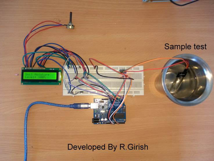

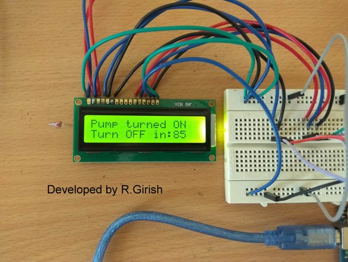 Once the pump is turned ON, it will display remaining time to turn off (in seconds).
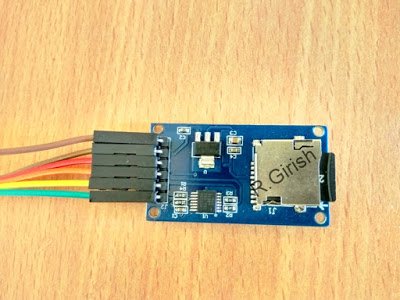
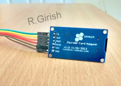 There are six pins and it supports SPI (serial peripheral interface) communication protocol.
For Arduino UNO the SPI communication pins are 13, 12, 11, and 10. For Arduino mega the SPI pins are 50, 51, 52 and 53.
The proposed project is illustrated with Arduino UNO if you have any other model of Arduino please refer internet for the SPI pins.
The module consists of a card holder which holds the SD card in place.
3.3V regulator is provided to limit the voltage to SD cards as it is designed to function at 3.3V and not 5V.
It has LVC125A integrated circuit on board which is logic level shifter.
The function of logic level shifter is to reduce 5V signals from arduino to 3.3V logic signals.
Now that concludes the SD card module.
Using SD card module we can store any king of data, here we are going to store text data.
We will be storing temperature and humidity data to SD card.
We are also utilizing real time clock module to log the time along with sensor data.
It records the data every 30 seconds.
There are six pins and it supports SPI (serial peripheral interface) communication protocol.
For Arduino UNO the SPI communication pins are 13, 12, 11, and 10. For Arduino mega the SPI pins are 50, 51, 52 and 53.
The proposed project is illustrated with Arduino UNO if you have any other model of Arduino please refer internet for the SPI pins.
The module consists of a card holder which holds the SD card in place.
3.3V regulator is provided to limit the voltage to SD cards as it is designed to function at 3.3V and not 5V.
It has LVC125A integrated circuit on board which is logic level shifter.
The function of logic level shifter is to reduce 5V signals from arduino to 3.3V logic signals.
Now that concludes the SD card module.
Using SD card module we can store any king of data, here we are going to store text data.
We will be storing temperature and humidity data to SD card.
We are also utilizing real time clock module to log the time along with sensor data.
It records the data every 30 seconds.

 The RTC module will keep track of time and log the date and time to the SD card.
The error LED blinks rapidly, if the SD card fails or fails to initialize or SD card not present.
Rest of the time the LED stay off.
The RTC module will keep track of time and log the date and time to the SD card.
The error LED blinks rapidly, if the SD card fails or fails to initialize or SD card not present.
Rest of the time the LED stay off.
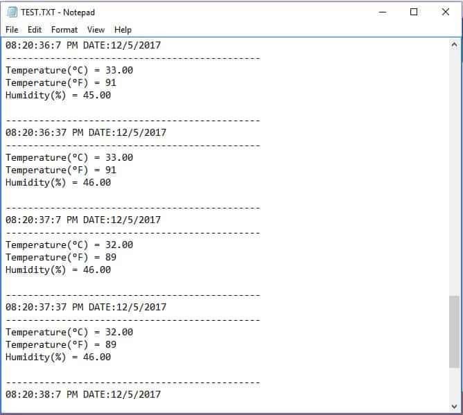 NOTE: The above idea is an example how to interface and record data.
The utilization of this project depend on your imagination, you can record sensor data of any kind.
NOTE: The above idea is an example how to interface and record data.
The utilization of this project depend on your imagination, you can record sensor data of any kind.
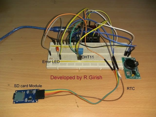
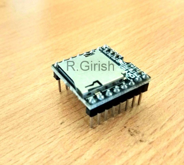 It has in-build amplifier which can drive 3 watt loudspeakers in stereo or mono.
It has 24-bit digital to analog converter (DAC) which is pretty good for such low cost and compact module.
It has in-build amplifier which can drive 3 watt loudspeakers in stereo or mono.
It has 24-bit digital to analog converter (DAC) which is pretty good for such low cost and compact module.
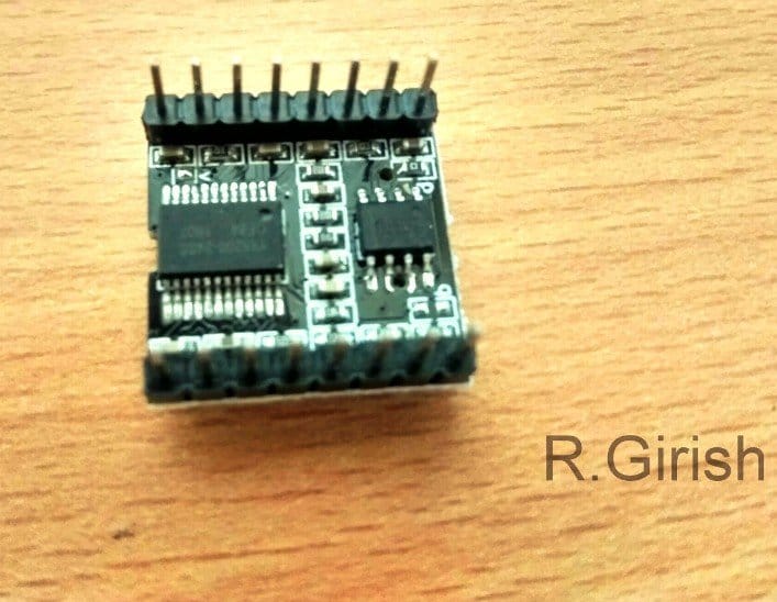 It supports MP3 and WMV hardware decoding.
It supports sampling rate of
8KHz,11.025KHz, 12KHz,1 6KHz, 22.05KHz, 24KHz, 32KHz, 44.1KHz, 48KHz.
It can support up to 32GB micro SD card.
It supports up to 100 folders, each folder can be assigned up to 1000 songs.
It has 6 different levels of equalizer; and 30 levels of volume adjust control.
It can operate from 3.2V to 5V.
It supports MP3 and WMV hardware decoding.
It supports sampling rate of
8KHz,11.025KHz, 12KHz,1 6KHz, 22.05KHz, 24KHz, 32KHz, 44.1KHz, 48KHz.
It can support up to 32GB micro SD card.
It supports up to 100 folders, each folder can be assigned up to 1000 songs.
It has 6 different levels of equalizer; and 30 levels of volume adjust control.
It can operate from 3.2V to 5V.
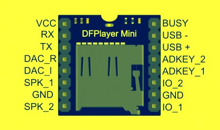 The above specifications are based on DFPlayerˇŻs data sheet.
By now you would have familiar with DFPlayer and its specification.
You can purchase this module from e-commerce sites or from local electronics market.
Now letˇŻs jump into the schematic diagram.
The above specifications are based on DFPlayerˇŻs data sheet.
By now you would have familiar with DFPlayer and its specification.
You can purchase this module from e-commerce sites or from local electronics market.
Now letˇŻs jump into the schematic diagram.
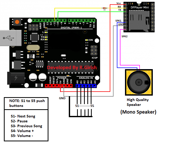 The above circuit is very simple; the arduino sends commands to the DFPlayer module to control the songs.
The user can input their choice via push buttons.
The arduinoˇŻs built-in pull-up resistor has been activated in the program, so that we no need to attach a physical resistor to push buttons.
Try to use good quality speakers; the DFPlayer can deliver very good quality sound.
If you find any distortion in the sound at higher volume levels, power the DFPlayer module externally at 5V DC with common ground connection between arduino and DFPlayer.
If you want stereo sound setup, connect the one of the speaker to SPK1 of DFPlayer and another speaker to SPK2 and ground the remaining speaker wires.
The above circuit is very simple; the arduino sends commands to the DFPlayer module to control the songs.
The user can input their choice via push buttons.
The arduinoˇŻs built-in pull-up resistor has been activated in the program, so that we no need to attach a physical resistor to push buttons.
Try to use good quality speakers; the DFPlayer can deliver very good quality sound.
If you find any distortion in the sound at higher volume levels, power the DFPlayer module externally at 5V DC with common ground connection between arduino and DFPlayer.
If you want stereo sound setup, connect the one of the speaker to SPK1 of DFPlayer and another speaker to SPK2 and ground the remaining speaker wires.
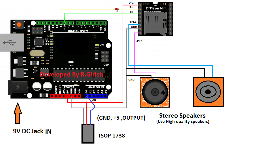 The above design is simple as the push button based; the only difference is removal of push buttons and inclusion of TSOP 1738 IR receiver.
The received signal from IR remote is fed to A0 pin of arduino.
Now to control this Mp3 player you need a spare TV, or any other IR based remote which might be lying on your junk box.
You have to decide which the buttons for controlling the functions like play & pause etc.
There are 6 functions:
1) Play and pause
2) Next song
3) Previous song
4) Volume increase
5) Volume decrease
6) Sound equalizer (Normal/Pop/Rock/Jazz/Classic/Base)
You need to choose the buttons on the remote and find its Hexadecimal codes of those buttons which will be transmitted by the remote.
To find the hexadecimal code, download the IR library if not done so.
github.com/z3t0/Arduino-IRremote
Add the library to arduino software and navigate to File> Examples> IRremote > IRrecvDemo and upload the code with completed hardware setup.
Open the serial monitor and press the buttons on remote, you will see the hexadecimal codes, note it down to corresponding button on piece of paper.
You need to enter the hexadecimal code on the program given below.
Once you entered the hexadecimal codes in the given program, upload it.
You are ready to control your songs from your remote.
The above design is simple as the push button based; the only difference is removal of push buttons and inclusion of TSOP 1738 IR receiver.
The received signal from IR remote is fed to A0 pin of arduino.
Now to control this Mp3 player you need a spare TV, or any other IR based remote which might be lying on your junk box.
You have to decide which the buttons for controlling the functions like play & pause etc.
There are 6 functions:
1) Play and pause
2) Next song
3) Previous song
4) Volume increase
5) Volume decrease
6) Sound equalizer (Normal/Pop/Rock/Jazz/Classic/Base)
You need to choose the buttons on the remote and find its Hexadecimal codes of those buttons which will be transmitted by the remote.
To find the hexadecimal code, download the IR library if not done so.
github.com/z3t0/Arduino-IRremote
Add the library to arduino software and navigate to File> Examples> IRremote > IRrecvDemo and upload the code with completed hardware setup.
Open the serial monitor and press the buttons on remote, you will see the hexadecimal codes, note it down to corresponding button on piece of paper.
You need to enter the hexadecimal code on the program given below.
Once you entered the hexadecimal codes in the given program, upload it.
You are ready to control your songs from your remote.
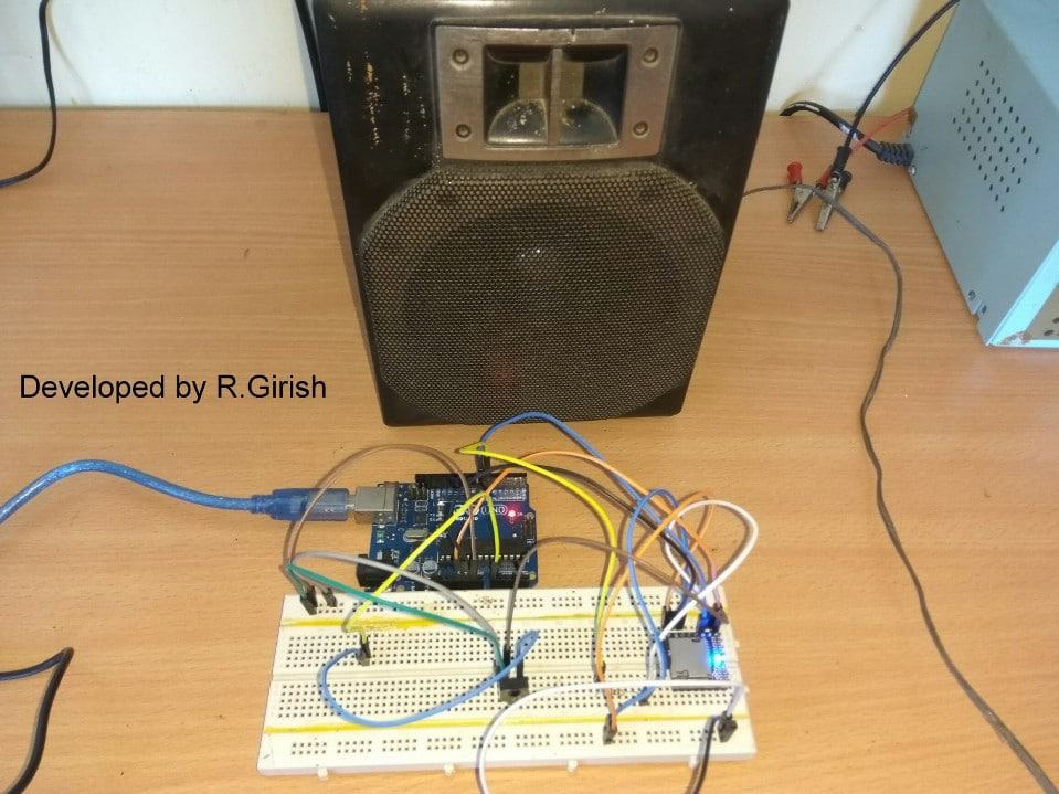
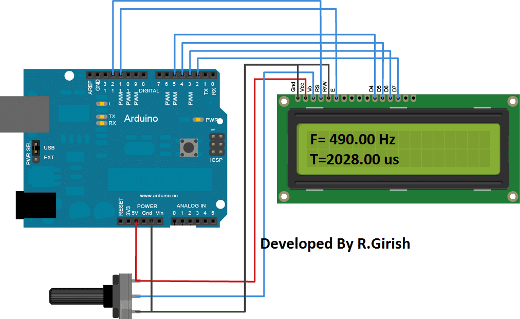 The above circuit is self-explanatory.
We can find similar connection between the display and arduino on other LCD based projects.
The 10K potentiometer is used to adjust the contrast of the 16 x 2 LCD display which must be set by the user for optimum view.
The above circuit is self-explanatory.
We can find similar connection between the display and arduino on other LCD based projects.
The 10K potentiometer is used to adjust the contrast of the 16 x 2 LCD display which must be set by the user for optimum view.
 The function of IC 7404 is to eliminate any noise signal from the input and fed to frequency sampling pin A0. The IC 7404 only outputs rectangular waves which is a great advantage for arduino, since arduino is more capable of processing digital signal than analogue signals.
Program:
The function of IC 7404 is to eliminate any noise signal from the input and fed to frequency sampling pin A0. The IC 7404 only outputs rectangular waves which is a great advantage for arduino, since arduino is more capable of processing digital signal than analogue signals.
Program:
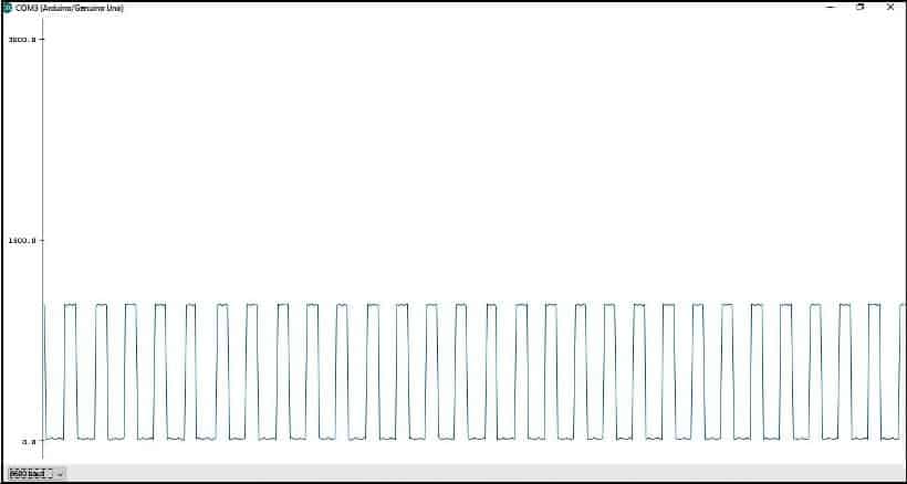 Press the push button to show the readings and also for refreshing the readings the LCD display, it must show around 490Hz on ˇ°test modeˇ±.
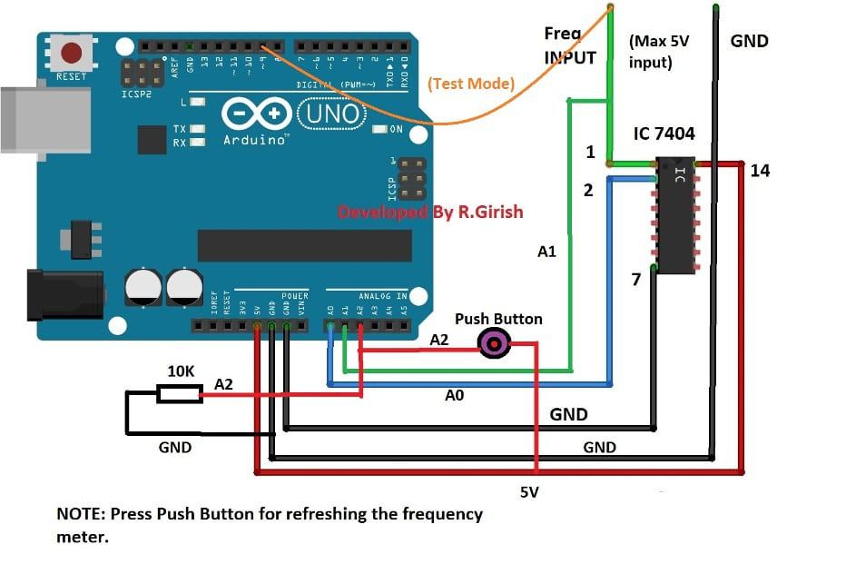 The test mode is to check proper functioning of the oscilloscope.
The pin #9 is programed to give 490Hz output.
The test mode is to check proper functioning of the oscilloscope.
The pin #9 is programed to give 490Hz output.
 A window will pop-up as illustrated below and select baud rate to 9600.
 Now select ˇ°Serial portˇ± tab and select the right COM port which can vary computer to computer.
If you select the correct COM port, you can see readings as illustrated below.
Now select ˇ°Serial portˇ± tab and select the right COM port which can vary computer to computer.
If you select the correct COM port, you can see readings as illustrated below.
 Now select ˇ°oscilloscopeˇ± tab and select ˇ°channels 1, 2 and 3ˇ± (first option).
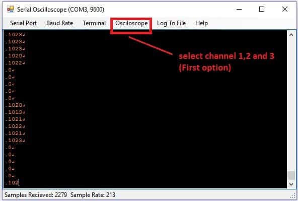
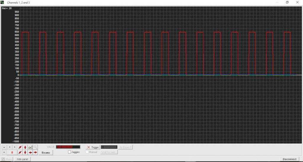 You can see the generated test signal from Arduino as illustrated below.
As you can see there are some control buttons on the software by which you can analyze the waveform better.
NOTE:
The proposed setup has one major disadvantage:
The Arduino cannot show input waveform on computer screen and frequency/time period reading on LCD display simultaneously.
To overcome this issue a push button is provided for reading/refresh the frequency and time period on the LCD display.
Once you press the button it will show the frequency and time period on LCD display at the same time waveform will freeze on the computer screen as long as you keep pressing the push button.
You may also consider this as an advantage since you can stop the frequency on the computer monitor at any instant and this may give you time to analyze displayed waveform.
You can see the generated test signal from Arduino as illustrated below.
As you can see there are some control buttons on the software by which you can analyze the waveform better.
NOTE:
The proposed setup has one major disadvantage:
The Arduino cannot show input waveform on computer screen and frequency/time period reading on LCD display simultaneously.
To overcome this issue a push button is provided for reading/refresh the frequency and time period on the LCD display.
Once you press the button it will show the frequency and time period on LCD display at the same time waveform will freeze on the computer screen as long as you keep pressing the push button.
You may also consider this as an advantage since you can stop the frequency on the computer monitor at any instant and this may give you time to analyze displayed waveform.

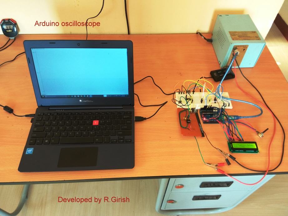 If you have any further queries regarding this simple single channel Arduino oscilloscope circuit, please feel free to use the below comment box for expressing your specific views
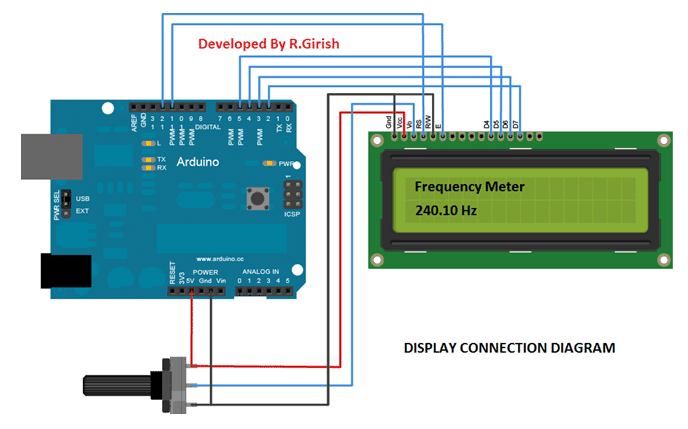 The above diagram is self-explanatory, the wiring connection between arduino and display is standard and we can find similar connections on other arduino and LCD based projects.
 The above diagram consists of inverter IC 7404. The role of IC 7404 is to eliminate noise from the input, so that the noise wonˇŻt propagate to arduino which might give false readings and IC 7404 can tolerate short spike voltage which will not pass to arduino pins.
IC 7404 only outputs rectangular waves where arduino can measure easily compare to analogue waves.
NOTE: The maximum peak to peak input should not exceed 5V.
The above diagram consists of inverter IC 7404. The role of IC 7404 is to eliminate noise from the input, so that the noise wonˇŻt propagate to arduino which might give false readings and IC 7404 can tolerate short spike voltage which will not pass to arduino pins.
IC 7404 only outputs rectangular waves where arduino can measure easily compare to analogue waves.
NOTE: The maximum peak to peak input should not exceed 5V.
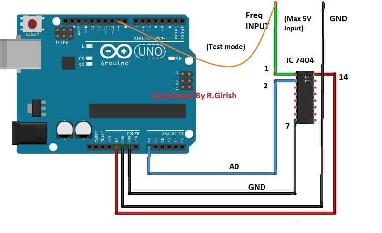 In the program pin #9 is enabled to give 490Hz at 50% duty cycle, the user can grab the input wire of the frequency meter and insert in pin #9 of arduino as shown in figure, we can see 490 Hz on the LCD display (with some tolerance), if the mentioned procedure was successful, you frequency meter is ready to serve you experiments.
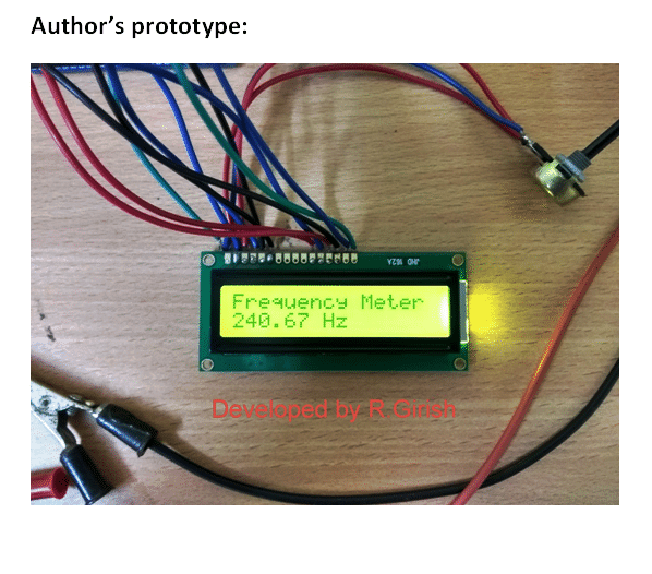
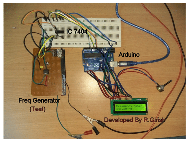 The user may also test this Arduino frequency meter circuit prototype by using external frequency generator which is shown in above image.
 Pin#8 and pin#9 generate the SPWMs alternately and switch the relevant mosfets with the same SPWM pattern.
The mosfst in turn induce the transformer with high current SPWM waveform using the battery power, causing the secondary of the trafo to generate an identical waveform but at the mains AC level.
The proposed Arduino inverter circuit could be upgraded to any preferred higher wattage level, simply by upgrading the mosfets and the trafo rating accordingly, alternatively you can also convert this into a full bridge or an H-bridge sine wave inverter
Pin#8 and pin#9 generate the SPWMs alternately and switch the relevant mosfets with the same SPWM pattern.
The mosfst in turn induce the transformer with high current SPWM waveform using the battery power, causing the secondary of the trafo to generate an identical waveform but at the mains AC level.
The proposed Arduino inverter circuit could be upgraded to any preferred higher wattage level, simply by upgrading the mosfets and the trafo rating accordingly, alternatively you can also convert this into a full bridge or an H-bridge sine wave inverter
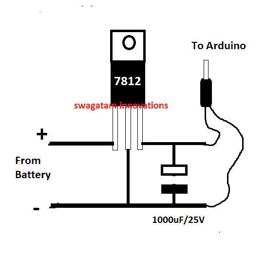 If you have any questions regarding the above SPWM inverter circuit using a programmed Arduino, please feel free to ask them through your valuable comments.
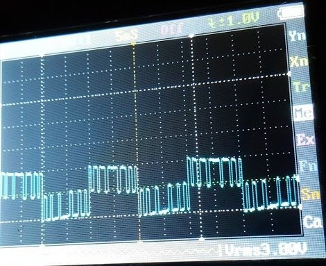 Image of SPWM waveform as obtained from the above Arduino inverter design (Tested and Submitted By Mr.
Ainsworth Lynch)
For the Program Code please visit the following link:
Arduino SPWM Generator Circuit
UPDATE:
Image of SPWM waveform as obtained from the above Arduino inverter design (Tested and Submitted By Mr.
Ainsworth Lynch)
For the Program Code please visit the following link:
Arduino SPWM Generator Circuit
UPDATE:
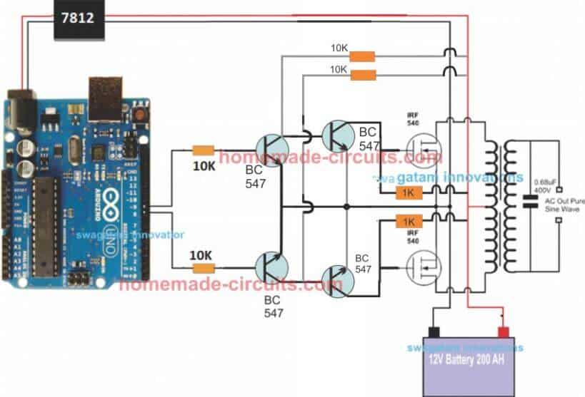 The above design is the recommended one! (Just make sure to add the delay timer, as explained below!!)
Video Clip
Parts List
All resistors are 1/4 watt, 5% CFR
10K = 4
1K = 2
BC547 = 4nos
Mosfets IRF540 = 2nos
Arduino UNO = 1
Transformer = 9-0-9V/220V/120V current as per requirement.
Battery = 12V, Ah value as per requirement
The above design is the recommended one! (Just make sure to add the delay timer, as explained below!!)
Video Clip
Parts List
All resistors are 1/4 watt, 5% CFR
10K = 4
1K = 2
BC547 = 4nos
Mosfets IRF540 = 2nos
Arduino UNO = 1
Transformer = 9-0-9V/220V/120V current as per requirement.
Battery = 12V, Ah value as per requirement
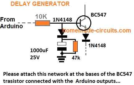 PLEASE TEST AND CONFIRM THE DELAY OUTPUT WITH AN LED AT THE COLLECTOR, BEFORE FINALIZING THE INVERTER.
FOR INCREASING THE DELAY YOU CAN INCREASE THE 10K VALUE TO 100K
PLEASE TEST AND CONFIRM THE DELAY OUTPUT WITH AN LED AT THE COLLECTOR, BEFORE FINALIZING THE INVERTER.
FOR INCREASING THE DELAY YOU CAN INCREASE THE 10K VALUE TO 100K
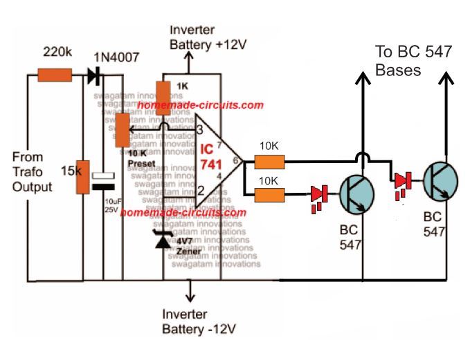 For an isolated version of voltage correction circuit we can modify the above circuit with a transformer, as shown below:
 Make sure to join the negative line with the battery negative
 Important:
In order to avoid an accidental switch ON prior to Arduino booting, a simple delay ON timer circuit may be included in the above design, as shown below:
Important:
In order to avoid an accidental switch ON prior to Arduino booting, a simple delay ON timer circuit may be included in the above design, as shown below:
 Video Demo
This constitutes one SPWM cycle, and this repeats throughout at a particular rate as determined by the application frequency (usually 50Hz or 60Hz).
Typically, SPWM is used for driving power devices such as mosfets or BJTs in inverters or converters.
This special modulation pattern ensures that the frequency cycles are executed with a gradually changing average voltage value (also called the RMS value) , instead of throwing sudden Hi/low voltage spikes as normally witnessed in flat square wave cycles.
This gradually modifying PWMs in a SPWM is purposely enforced so that it closely replicates the exponentially rising/falling pattern of a standard sinewaves or sinusoidal waveform, hence the name sinewave PWM or SPWM.
Video Demo
This constitutes one SPWM cycle, and this repeats throughout at a particular rate as determined by the application frequency (usually 50Hz or 60Hz).
Typically, SPWM is used for driving power devices such as mosfets or BJTs in inverters or converters.
This special modulation pattern ensures that the frequency cycles are executed with a gradually changing average voltage value (also called the RMS value) , instead of throwing sudden Hi/low voltage spikes as normally witnessed in flat square wave cycles.
This gradually modifying PWMs in a SPWM is purposely enforced so that it closely replicates the exponentially rising/falling pattern of a standard sinewaves or sinusoidal waveform, hence the name sinewave PWM or SPWM.
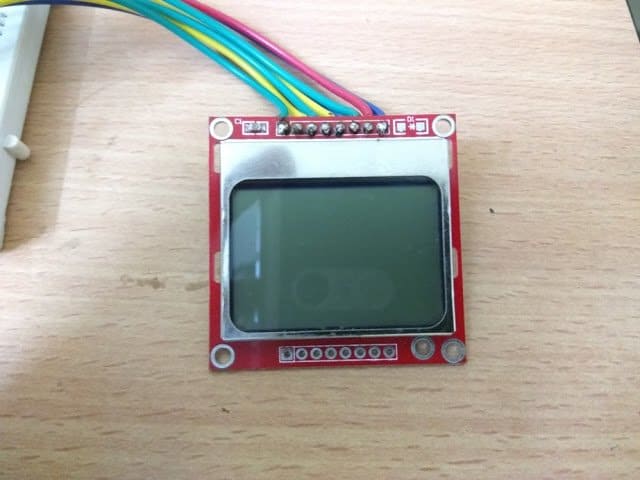 Fun fact: Nokia 5110 display was also used in 3310 model and some more other Nokia phone models too.
Now letˇŻs see how to connect the display with arduino.
Fun fact: Nokia 5110 display was also used in 3310 model and some more other Nokia phone models too.
Now letˇŻs see how to connect the display with arduino.
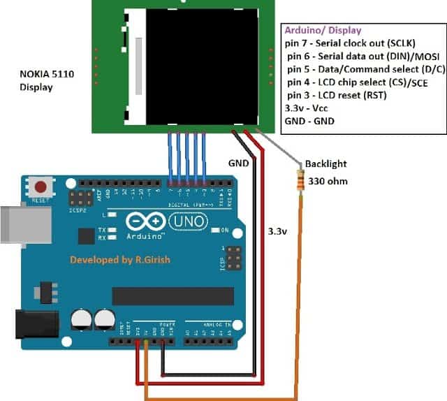 The display is monochrome and it has 84x48 pixels which can display text and even graphics.
The display consists of 8 pins: Vcc, GND, reset, chip select (CS), command select, serial data out, Serial clock and backlight.
The display is designed to work at 3.3V and applying 5V will damage the display, so care must be taken while handling it.
The display has backlight functionality which is commonly in white or blue in colour.
5V is given to backlight with 330 ohm current limiting resistor.
Pins 7, 6, 5, 4 and 3 are connected to the digital pins of the display.
It is not mandatory to know how the arduino communicates with display in order to use it; we will add appropriate library files to the arduino software which will take care of the communication between arduino and display.
Now letˇŻs display some text.
The display is monochrome and it has 84x48 pixels which can display text and even graphics.
The display consists of 8 pins: Vcc, GND, reset, chip select (CS), command select, serial data out, Serial clock and backlight.
The display is designed to work at 3.3V and applying 5V will damage the display, so care must be taken while handling it.
The display has backlight functionality which is commonly in white or blue in colour.
5V is given to backlight with 330 ohm current limiting resistor.
Pins 7, 6, 5, 4 and 3 are connected to the digital pins of the display.
It is not mandatory to know how the arduino communicates with display in order to use it; we will add appropriate library files to the arduino software which will take care of the communication between arduino and display.
Now letˇŻs display some text.
 Before you upload the code you must download the library files and add to your arduino IDE.
github.com/adafruit/Adafruit-PCD8544-Nokia-5110-LCD-library
github.com/adafruit/Adafruit-GFX-Library
Before you upload the code you must download the library files and add to your arduino IDE.
github.com/adafruit/Adafruit-PCD8544-Nokia-5110-LCD-library
github.com/adafruit/Adafruit-GFX-Library
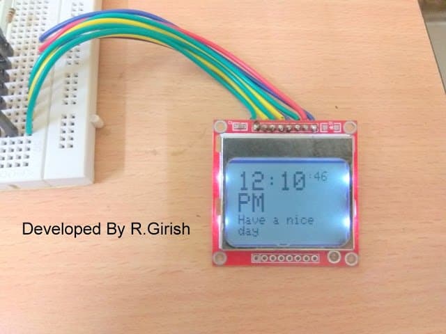
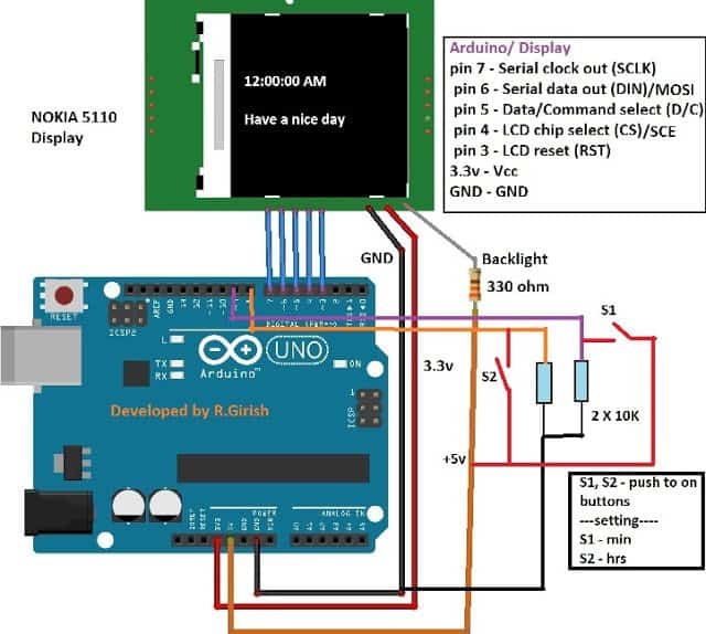 The schematic is same as previous one, only the difference is the two 10K ohm pull-down resistors for setting time are connect to pin #8 and pin # 9; rest of the circuit is self-explanatory.
 Dr.
A.P.J Abdul Kalam:
Dr.
A.P.J Abdul Kalam:
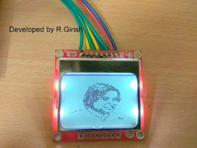 As we can see that using a monochrome display, still we are able display some photos or logos directly from arduino.
We no need any kind of external memory such as SD card.
The process of converting a photo into ˇ°Cˇ± code is subject of another article, where we will be illustrating step by step process.
If you have any queries, please express through the comment section.
As we can see that using a monochrome display, still we are able display some photos or logos directly from arduino.
We no need any kind of external memory such as SD card.
The process of converting a photo into ˇ°Cˇ± code is subject of another article, where we will be illustrating step by step process.
If you have any queries, please express through the comment section.
 The above diagram shows the wiring diagram.
This sensor needs external 5V supply because it has heating element inside the sensor which consumes around 1 Watt.
The power from arduinoˇ®s power pin canˇŻt supply higher current.
The heating element keeps the sensor warm and helps to sample appropriate amount of chemical concentration in air.
The sensor takes about couple of minutes to reach optimum temperature.
The above diagram shows the wiring diagram.
This sensor needs external 5V supply because it has heating element inside the sensor which consumes around 1 Watt.
The power from arduinoˇ®s power pin canˇŻt supply higher current.
The heating element keeps the sensor warm and helps to sample appropriate amount of chemical concentration in air.
The sensor takes about couple of minutes to reach optimum temperature.

 The circuit connection from sensor to arduino is very simple.
The output of the sensor is connected to A1 pin of arduino.
The supply Vcc and GND are connected to power supply pins of arduino.
Note: Please make sure that your sensor has built in pull-up resistor, if it doesnˇŻt have one; connect a 4.7K pull-up resistor at output pin of the DHT11 sensor.
The circuit connection from sensor to arduino is very simple.
The output of the sensor is connected to A1 pin of arduino.
The supply Vcc and GND are connected to power supply pins of arduino.
Note: Please make sure that your sensor has built in pull-up resistor, if it doesnˇŻt have one; connect a 4.7K pull-up resistor at output pin of the DHT11 sensor.

 It uses I2C communication protocol, the SDA pin goes to A4 of arduino and SCL goes to A5 of arduino.
The Vcc and GND are connected to power supply pins of arduino.
It uses I2C communication protocol, the SDA pin goes to A4 of arduino and SCL goes to A5 of arduino.
The Vcc and GND are connected to power supply pins of arduino.

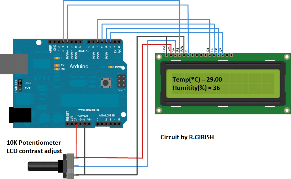 The LCD display shows all the data from the sensors.
The connection between LCD display and arduino is standard; we can find similar connection on many other LCD based projects.
Adjust the 10K potentiometer for optimum visibility from the LCD display.
The LCD display shows all the data from the sensors.
The connection between LCD display and arduino is standard; we can find similar connection on many other LCD based projects.
Adjust the 10K potentiometer for optimum visibility from the LCD display.

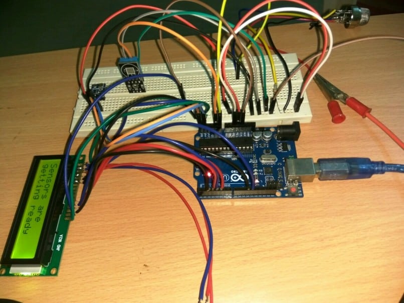 Here is the authorˇŻs prototype of a mini weather monitor circuit where all the sensor shown in the schematics are connected to the arduino board.
Note: The circuit connection from each sensors and LCD display should be connected to single arduino board.
We have given discrete sensor connection on each schematic to avoid confusion while duplicating the circuit.
Download the Library files before uploading the code:
DHT11 library: https://arduino-info.wikispaces.com/file/detail/DHT-lib.zip
BMP180 library: github.com/adafruit/Adafruit_BMP085_Unified.git
Here is the authorˇŻs prototype of a mini weather monitor circuit where all the sensor shown in the schematics are connected to the arduino board.
Note: The circuit connection from each sensors and LCD display should be connected to single arduino board.
We have given discrete sensor connection on each schematic to avoid confusion while duplicating the circuit.
Download the Library files before uploading the code:
DHT11 library: https://arduino-info.wikispaces.com/file/detail/DHT-lib.zip
BMP180 library: github.com/adafruit/Adafruit_BMP085_Unified.git

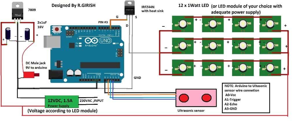 The automatic street light dimmer circuit consist of Arduino which is the brain of the project, an ultrasonic sensor for detecting vehicles or human beings.
A 9V regulator is provided for powering the arduino microcontroller board and a MOSFET for driving the LEDs which consumes few amperes at peak brightness.
The LED module and power supply for the setup must be selected carefully so that there will be adequate power available for the whole circuit and does not overload the power supply.
The LED module can be homemade one which is shown in schematic or may be purchased for market, but before constructing or getting one form market make sure to calculate the voltage and current requirements for the power supply.
The power supply may be an SMPS or constructed using transformer, rectifier and voltage regulator.
The LED reduces its brightness by using PWM.
The PWM is square wave, it turns on and off supply to LED rapidly with well determined on and off width in a single cycle.
The width of the on and off time determine the brightness of the LED.
When the street light switches to full brightness the supply to LED will have no pulses and steady DC will be supplied.
The whole setup can be implemented as shown below:
The automatic street light dimmer circuit consist of Arduino which is the brain of the project, an ultrasonic sensor for detecting vehicles or human beings.
A 9V regulator is provided for powering the arduino microcontroller board and a MOSFET for driving the LEDs which consumes few amperes at peak brightness.
The LED module and power supply for the setup must be selected carefully so that there will be adequate power available for the whole circuit and does not overload the power supply.
The LED module can be homemade one which is shown in schematic or may be purchased for market, but before constructing or getting one form market make sure to calculate the voltage and current requirements for the power supply.
The power supply may be an SMPS or constructed using transformer, rectifier and voltage regulator.
The LED reduces its brightness by using PWM.
The PWM is square wave, it turns on and off supply to LED rapidly with well determined on and off width in a single cycle.
The width of the on and off time determine the brightness of the LED.
When the street light switches to full brightness the supply to LED will have no pulses and steady DC will be supplied.
The whole setup can be implemented as shown below:

 -The ultrasonic sensor is elevated around 3.5ft to 4ft above the ground; this is done so that it only detects vehicles and human beings, since their average height is around the same and when dogs or cats or any other animals which usually roam around the city will not trigger the street light to maximum brightness.
The animals which live and roam around the city are below 3.5ft tall.
The sensor height may be adjusted to operate at optimum level as described in the above picture.
The threshold distance can be controlled in the program.
When the Arduino detects the obstacle detected below pre-determined distance the LED lights go peak brightness.
-The ultrasonic sensor is elevated around 3.5ft to 4ft above the ground; this is done so that it only detects vehicles and human beings, since their average height is around the same and when dogs or cats or any other animals which usually roam around the city will not trigger the street light to maximum brightness.
The animals which live and roam around the city are below 3.5ft tall.
The sensor height may be adjusted to operate at optimum level as described in the above picture.
The threshold distance can be controlled in the program.
When the Arduino detects the obstacle detected below pre-determined distance the LED lights go peak brightness.
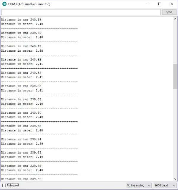 If you have any further questions regarding this Arduino based automatic street light dimmer circuit feel free to ask in comment section.
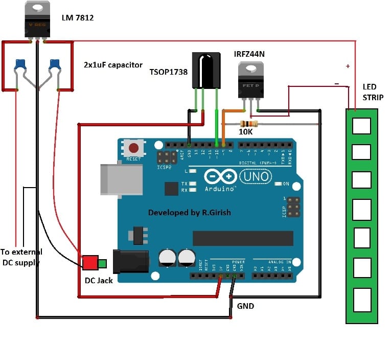 The circuit consists of few components: voltage regulator with coupling capacitors, TSOP1738 IR sensor, MOSFET IRFZ44N, LED strip and brain of the project arduino Uno.
You can choose your favourite arduino board for this project.
The TSOP1738 sensor receives IR signals from the remote and decode in such a way that microcontroller can understood.
The N-channel MOSFET amplify the signals from arduino and fed to LED strip.
The voltage regulator powers arduino and LED strip.
Make sure your power supply can deliver adequate amount of current for LED strip.
The proposed circuit is designed for 12V LED strips, you can change voltage regulator depending on LED strip specification.
It is advised not to use a LED strip which has voltage rating higher than 20V, as arduinoˇŻs absolute maximum is 20V.
This circuit can turn on and off the LED strip; it can adjust brightness up and down by 5 steps, this is achieved by applying different PWM signals to LED strip.
The circuit consists of few components: voltage regulator with coupling capacitors, TSOP1738 IR sensor, MOSFET IRFZ44N, LED strip and brain of the project arduino Uno.
You can choose your favourite arduino board for this project.
The TSOP1738 sensor receives IR signals from the remote and decode in such a way that microcontroller can understood.
The N-channel MOSFET amplify the signals from arduino and fed to LED strip.
The voltage regulator powers arduino and LED strip.
Make sure your power supply can deliver adequate amount of current for LED strip.
The proposed circuit is designed for 12V LED strips, you can change voltage regulator depending on LED strip specification.
It is advised not to use a LED strip which has voltage rating higher than 20V, as arduinoˇŻs absolute maximum is 20V.
This circuit can turn on and off the LED strip; it can adjust brightness up and down by 5 steps, this is achieved by applying different PWM signals to LED strip.
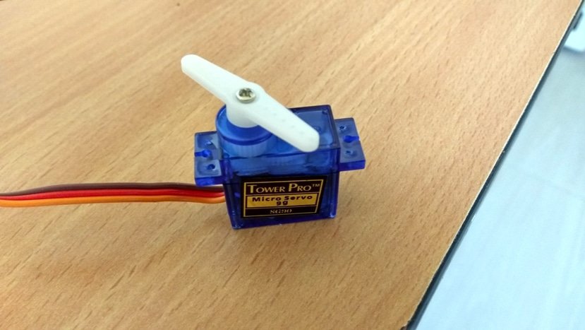 The servo motors are used in robotics, CCTV cameras, RC cars, boats, toy aircrafts etc.
Servos are used where we no need continues rotatory motion, but lock in a specific position or move some load with controlled velocity within the moveable angular limit.
Servo arenˇŻt simply a motor like other types, but it is module, which combines of a normal DC/AC motor, a group of gears, control electronics and a feedback system.
LetˇŻs look at the each mentioned stages in detail.
DC/AC motor which is employed on a servo module can be brushless or brushed motor, on most of the hobby servos DC motor is used and AC motors are used in industrial applications.
The motor gives rotational input to the servo.
The motor rotates at several hundred RPM inside the servo and output rotation is about 50 or more times less of its RPM.
The next stage is the gear assembly, which control the angular rotation and speed of servo.
The gear may be made from either plastic or metal depending on how bulky the load is.
Generally DC motors are run at high RPM and low torque; the gear assembly will convert the excess RPM into torque.
Thus a small motor can handle a huge load.
The next stage is control electronics which constitutes of MOSFETs and ICs for controlling the rotation of the motor.
A feedback system is always present in servo motors for tracking the current position of the actuator.
In servos generally a feedback component is a potentiometer, which is directly connected to rotating actuator.
The potentiometer acts as voltage divider which is fed to the control electronics.
This feedback helps control electronics to determine the amount of power given to the motor.
A servo motor in a fixed position will reluctant move from its current position if any external force try to disturb.
The feedback system monitors the current position and powers the motor against external disturbance.
The above scenario is same when the servo is moving its actuator.
The control system will compensate the external force and move in determined velocity.
By now you know quite a bit about servo motor and its functioning mechanism.
LetˇŻs see how to control the servo motors using microcontroller.
Servo motors have 3 terminals unlike other motors which have 2 terminals, two for supply (5V nominal) and one for control signal.
The wires are coloured for easy identification of terminals.
The control signals of servos are PWM at 50Hz frequency.
The pulse width of the signal determines the position of the actuator arm.
A typical hobby servo motor operates from 1 to 2 milliseconds pulse width.
Applying 1 ms pulse width control signal will keep the actuator at 0 degree position.
Applying 2 ms pulse width control signal will keep the actuator at 180 degree position.
Applying signals in between 1-2 ms will keep the actuator within 0-180 degree angle.
This can be better understood by given below image.
The servo motors are used in robotics, CCTV cameras, RC cars, boats, toy aircrafts etc.
Servos are used where we no need continues rotatory motion, but lock in a specific position or move some load with controlled velocity within the moveable angular limit.
Servo arenˇŻt simply a motor like other types, but it is module, which combines of a normal DC/AC motor, a group of gears, control electronics and a feedback system.
LetˇŻs look at the each mentioned stages in detail.
DC/AC motor which is employed on a servo module can be brushless or brushed motor, on most of the hobby servos DC motor is used and AC motors are used in industrial applications.
The motor gives rotational input to the servo.
The motor rotates at several hundred RPM inside the servo and output rotation is about 50 or more times less of its RPM.
The next stage is the gear assembly, which control the angular rotation and speed of servo.
The gear may be made from either plastic or metal depending on how bulky the load is.
Generally DC motors are run at high RPM and low torque; the gear assembly will convert the excess RPM into torque.
Thus a small motor can handle a huge load.
The next stage is control electronics which constitutes of MOSFETs and ICs for controlling the rotation of the motor.
A feedback system is always present in servo motors for tracking the current position of the actuator.
In servos generally a feedback component is a potentiometer, which is directly connected to rotating actuator.
The potentiometer acts as voltage divider which is fed to the control electronics.
This feedback helps control electronics to determine the amount of power given to the motor.
A servo motor in a fixed position will reluctant move from its current position if any external force try to disturb.
The feedback system monitors the current position and powers the motor against external disturbance.
The above scenario is same when the servo is moving its actuator.
The control system will compensate the external force and move in determined velocity.
By now you know quite a bit about servo motor and its functioning mechanism.
LetˇŻs see how to control the servo motors using microcontroller.
Servo motors have 3 terminals unlike other motors which have 2 terminals, two for supply (5V nominal) and one for control signal.
The wires are coloured for easy identification of terminals.
The control signals of servos are PWM at 50Hz frequency.
The pulse width of the signal determines the position of the actuator arm.
A typical hobby servo motor operates from 1 to 2 milliseconds pulse width.
Applying 1 ms pulse width control signal will keep the actuator at 0 degree position.
Applying 2 ms pulse width control signal will keep the actuator at 180 degree position.
Applying signals in between 1-2 ms will keep the actuator within 0-180 degree angle.
This can be better understood by given below image.
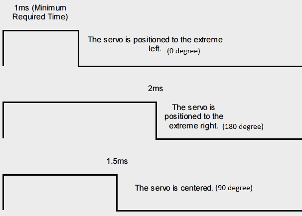 By now you would have understood how a servo is controlled by pulse width modulation (PWM).
Now letˇŻs learn how to interface a servo motor with Arduino.
By now you would have understood how a servo is controlled by pulse width modulation (PWM).
Now letˇŻs learn how to interface a servo motor with Arduino.
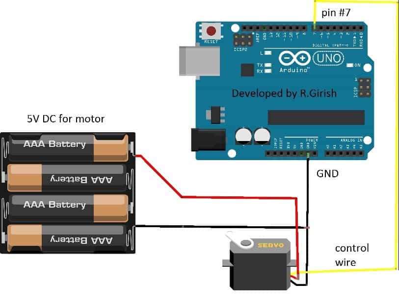 The wiring is easy and self-explanatory.
You need external power supply if you are using a bulky servo motor.
If you try to power from arduino powerˇŻs supply you will end-up overloading the USB port on the computer.
If you have servo similar which is illustrated at the beginning of the article, then you may power it from arduino 5V supply, also shown in authorˇŻs prototype.
The wiring is easy and self-explanatory.
You need external power supply if you are using a bulky servo motor.
If you try to power from arduino powerˇŻs supply you will end-up overloading the USB port on the computer.
If you have servo similar which is illustrated at the beginning of the article, then you may power it from arduino 5V supply, also shown in authorˇŻs prototype.
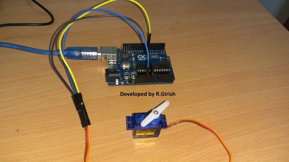 Arduino need servo library for handling it, it made our task easy and itˇŻs already in the Arduino IDE.
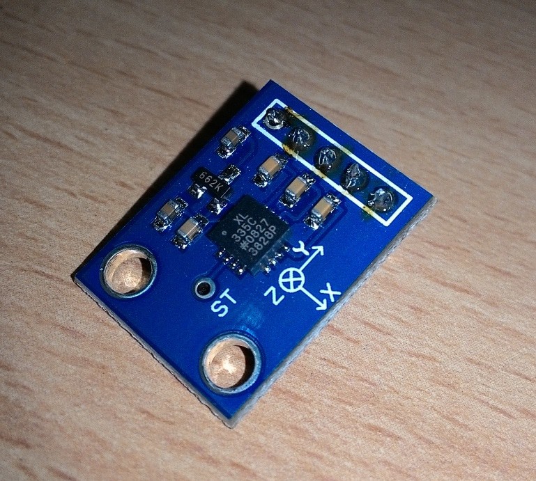 Accelerometer can be single, double or triple axis; here we are using triple axis accelerometer which can detect acceleration in 3 axes i.e.
X, Y and Z.
This means it has three such moving capacitors placed in X, Y and Z directions fabricated into single IC module.
If you want to know more about accelerometers, you can check out this link which explains how accelerometer works.
The accelerometer used in this project has analogue voltage output with respect to external acceleration.
To use it on digital circuits, we need to convert the analogue voltage into digital.
The process for converting analogue to digital conversion can be easily accomplished by arduino.
Accelerometer can be single, double or triple axis; here we are using triple axis accelerometer which can detect acceleration in 3 axes i.e.
X, Y and Z.
This means it has three such moving capacitors placed in X, Y and Z directions fabricated into single IC module.
If you want to know more about accelerometers, you can check out this link which explains how accelerometer works.
The accelerometer used in this project has analogue voltage output with respect to external acceleration.
To use it on digital circuits, we need to convert the analogue voltage into digital.
The process for converting analogue to digital conversion can be easily accomplished by arduino.

 The discussed Arduino accelerometer circuit is very simple as we are only going to extract readings from the accelerometer.
The accelerometer has 5 terminals Vcc, GND, X, Y and Z terminals.
The X, Y and Z axes terminals are connected to A2, A1 and A0 terminals of arduino respectively.
The accelerometer can be powered from 3.3V port on arduino.
Please take at-most care while powering from external power supplies for projects, 5V can easily damage the accelerometer, it has absolute maximum voltage of 3.6V.
The discussed Arduino accelerometer circuit is very simple as we are only going to extract readings from the accelerometer.
The accelerometer has 5 terminals Vcc, GND, X, Y and Z terminals.
The X, Y and Z axes terminals are connected to A2, A1 and A0 terminals of arduino respectively.
The accelerometer can be powered from 3.3V port on arduino.
Please take at-most care while powering from external power supplies for projects, 5V can easily damage the accelerometer, it has absolute maximum voltage of 3.6V.
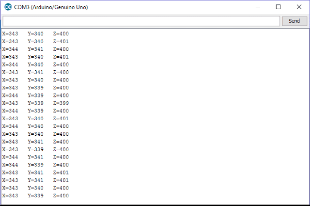 What we can infer from the serial monitor is the voltage level from the accelerometerˇŻs three different axes.
When it is subjected external force or tilt it gets reflected in the serial monitor.
We can program the arduino trigger some external peripherals such as relay or LED or motor, when the acceleration or tilt is subject to go beyond pre-determined threshold but, it is subject of an another article.
What we can infer from the serial monitor is the voltage level from the accelerometerˇŻs three different axes.
When it is subjected external force or tilt it gets reflected in the serial monitor.
We can program the arduino trigger some external peripherals such as relay or LED or motor, when the acceleration or tilt is subject to go beyond pre-determined threshold but, it is subject of an another article.
 The air pollution meter will be more interesting if the LEDs are rectangular shaped and above layout design is used.
However, you can use your imagination to make this project more interesting to you.
The air pollution meter will be more interesting if the LEDs are rectangular shaped and above layout design is used.
However, you can use your imagination to make this project more interesting to you.
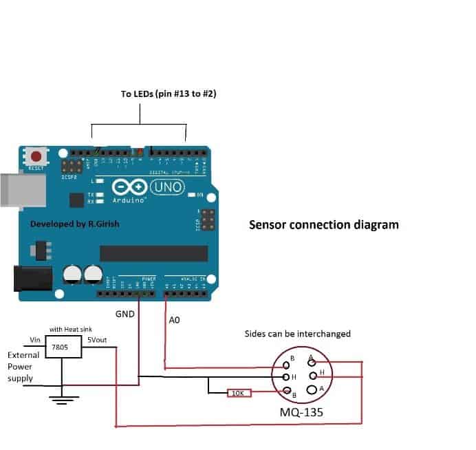 The above schematic illustrates, how to connect sensor to arduino.
An external power supply is implemented for heater coil of the sensor.
The sides of the sensor can be interchanged.
The pin A0 of arduino senses the voltage variations in the sensor due to changes in pollution content in air.
The sensor acts as variable resistor (in response to pollution) and 10K is fixed resistor, this act as a voltage divider.
The arduino has 10-bit ADC, which helps the LED to glow discretely in response to air pollution level, which is an analogue function.
The above schematic illustrates, how to connect sensor to arduino.
An external power supply is implemented for heater coil of the sensor.
The sides of the sensor can be interchanged.
The pin A0 of arduino senses the voltage variations in the sensor due to changes in pollution content in air.
The sensor acts as variable resistor (in response to pollution) and 10K is fixed resistor, this act as a voltage divider.
The arduino has 10-bit ADC, which helps the LED to glow discretely in response to air pollution level, which is an analogue function.
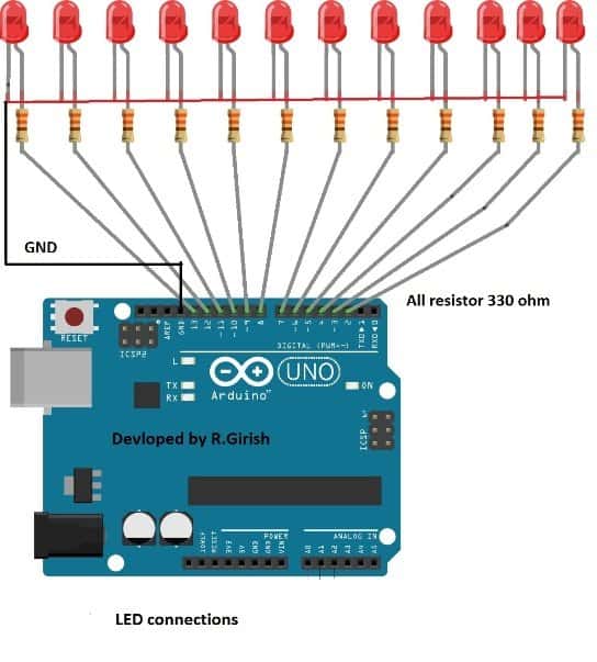 When the analogue voltage level crosses a certain threshold level which is pre-determined in the program, it will turn on LEDs.
The successive LEDs are pre-determined with higher threshold levels.
It starts with LED test, each LED is turned on sequentially with some delay and the user can determine the error in the LED connections, such as unconnected LEDs and LEDs which are not sorted sequentially.
The program comes to halt for 5 minutes and all the LEDs glow simultaneously.
This will give enough time for the sensor to warm-up; we can see some of the action performed by arduino in serial monitor.
Once sensor reaches optimum temperature, arduino sends some readings to serial monitor.
Based on the readings, LEDs will turn ON and OFF.
Higher the values print on serial monitor, more number of LEDs turns on.
The serial monitor is not mandatory in this project, but can be a handy tool for testing purposes.
When the analogue voltage level crosses a certain threshold level which is pre-determined in the program, it will turn on LEDs.
The successive LEDs are pre-determined with higher threshold levels.
It starts with LED test, each LED is turned on sequentially with some delay and the user can determine the error in the LED connections, such as unconnected LEDs and LEDs which are not sorted sequentially.
The program comes to halt for 5 minutes and all the LEDs glow simultaneously.
This will give enough time for the sensor to warm-up; we can see some of the action performed by arduino in serial monitor.
Once sensor reaches optimum temperature, arduino sends some readings to serial monitor.
Based on the readings, LEDs will turn ON and OFF.
Higher the values print on serial monitor, more number of LEDs turns on.
The serial monitor is not mandatory in this project, but can be a handy tool for testing purposes.
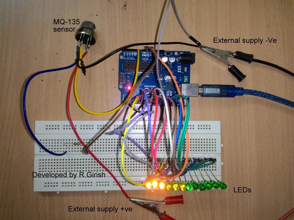
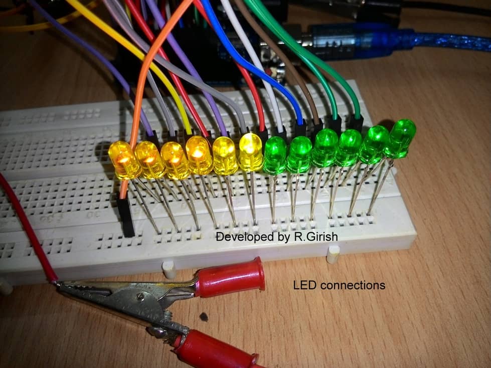
 The TX of GSM is connected to pin #9 of Arduino and RX of the GSM is connected to pin #8 of Arduino and ground to ground connection is also connected.
The power and data connection of the sensor is optimized for reduced wiring congestion while prototyping.
Please note the connections carefully and insert the sensor from A0 to A2 in correct orientation as illustrated below.
The TX of GSM is connected to pin #9 of Arduino and RX of the GSM is connected to pin #8 of Arduino and ground to ground connection is also connected.
The power and data connection of the sensor is optimized for reduced wiring congestion while prototyping.
Please note the connections carefully and insert the sensor from A0 to A2 in correct orientation as illustrated below.
 Reversing the orientation of the sensor will give out ˇ°NO DATAˇ± on the serial monitor.
If reverse orientation is kept for prolonged period it may even damage the sensor.
So, be cautious about the sensor connection.
Reversing the orientation of the sensor will give out ˇ°NO DATAˇ± on the serial monitor.
If reverse orientation is kept for prolonged period it may even damage the sensor.
So, be cautious about the sensor connection.
 Always power the GSM modem with external power supply.
A 9V 500mA power adapter will be enough for GSM modem.
The serial monitor is not mandatory for this project as it is going to be a standalone project.
We need serial monitor only while testing the prototype.
Make a DC UPS system, schematics is available in this website and try to make the power button easily accessible outside the chassis of your project, so that GSM modem can be powered ON after a brief power failure.
The external power button can be made by soldering wires from pins of the power button on the GSM modem.
DC UPS will reduce necessity to power ON the GSM modem after every power failure.
It gives plug and forget kind of feature.
Now letˇŻs see how the whole setup functions.
In case of fire the room temperature rises rapidly in short period, the sensor has the ability to measure form 0 to 50 degree Celsius.
When the temperature rises above the preset threshold value in the program (within 0 to 50) it sends SMS alert saying ˇ°Fire alert: 45.00 degree Celsiusˇ±.
45 degree Celsius is the temperature of the room during sending SMS; the temperature would reach beyond 100 degree Celsius within minutes after fire accident.
Two SMS alert is send for redundancy, in case if the one of the sent message is failed.
If the sensor failed or the sensor gets disconnected from Arduino, the information is send to the user via SMS twice saying ˇ°No data from sensor/sensor disconnectedˇ°
The program comes to halt for 30 minutes after sending SMS alert for fire or sensor disconnection.
It checks again for abnormality in room temperature and sensor wire connection after 30 minutes, if any exist, it sending SMS alert again and waits for another 30 minutes.
When the whole setup is completed and powered ON, the GSM modem sends test SMS saying ˇ°This is a test SMS from GSM modemˇ± if you receive this message to the recipient number, it means your project is working fine.
Always power the GSM modem with external power supply.
A 9V 500mA power adapter will be enough for GSM modem.
The serial monitor is not mandatory for this project as it is going to be a standalone project.
We need serial monitor only while testing the prototype.
Make a DC UPS system, schematics is available in this website and try to make the power button easily accessible outside the chassis of your project, so that GSM modem can be powered ON after a brief power failure.
The external power button can be made by soldering wires from pins of the power button on the GSM modem.
DC UPS will reduce necessity to power ON the GSM modem after every power failure.
It gives plug and forget kind of feature.
Now letˇŻs see how the whole setup functions.
In case of fire the room temperature rises rapidly in short period, the sensor has the ability to measure form 0 to 50 degree Celsius.
When the temperature rises above the preset threshold value in the program (within 0 to 50) it sends SMS alert saying ˇ°Fire alert: 45.00 degree Celsiusˇ±.
45 degree Celsius is the temperature of the room during sending SMS; the temperature would reach beyond 100 degree Celsius within minutes after fire accident.
Two SMS alert is send for redundancy, in case if the one of the sent message is failed.
If the sensor failed or the sensor gets disconnected from Arduino, the information is send to the user via SMS twice saying ˇ°No data from sensor/sensor disconnectedˇ°
The program comes to halt for 30 minutes after sending SMS alert for fire or sensor disconnection.
It checks again for abnormality in room temperature and sensor wire connection after 30 minutes, if any exist, it sending SMS alert again and waits for another 30 minutes.
When the whole setup is completed and powered ON, the GSM modem sends test SMS saying ˇ°This is a test SMS from GSM modemˇ± if you receive this message to the recipient number, it means your project is working fine.
 GSM modem is a hardware which accepts a valid SIM card (Subscriber Identity Module), basically any SIM will work, which supports GSM protocol and with a network subscription.
It is like a mobile phone without Screen and keypad.
It has four I/O pins depending on the model you choose.
Two for TX and RX (transmit and receive), another two pins for VCC and GND, which is common in all.
It also consist of RS232 port for serial communication between the modem and computer, however we are not going to use in this project.
It has standard DC power jack, which can be powered from external power sources such as voltage adapters.
It has working voltage ranging from 5 to 12V on DC jack, depending on the model.
It has 3 LED indicators, for power, status, and network.
The power LED indicates the presence of power, status LED indicates whether the GSM modem is operating or not, the Network LED indicates the establishment of mobile network.
Initially network LED blinks every one second while searching for network, once it establishes the mobile network it blinks every 3 seconds.
You need to press power button for 2 to 3 seconds for activating the GSM modem, once you done, it latch to the mobile network.
To verify that your GSM modem works, just call the number of which you have inserted the SIM card.
You should get ring back tone.
If it does, then your module is working fine.
We are going to use SIM800 GSM modem which supports quad-band 850/900/1800/1900 MHz.
if you own a SIM900 modem, need not to worry, the program and circuit is compatible in this project.
Now, you would have gained some idea about GSM modem, now letˇŻs learn how to interface it with arduino.
GSM modem is a hardware which accepts a valid SIM card (Subscriber Identity Module), basically any SIM will work, which supports GSM protocol and with a network subscription.
It is like a mobile phone without Screen and keypad.
It has four I/O pins depending on the model you choose.
Two for TX and RX (transmit and receive), another two pins for VCC and GND, which is common in all.
It also consist of RS232 port for serial communication between the modem and computer, however we are not going to use in this project.
It has standard DC power jack, which can be powered from external power sources such as voltage adapters.
It has working voltage ranging from 5 to 12V on DC jack, depending on the model.
It has 3 LED indicators, for power, status, and network.
The power LED indicates the presence of power, status LED indicates whether the GSM modem is operating or not, the Network LED indicates the establishment of mobile network.
Initially network LED blinks every one second while searching for network, once it establishes the mobile network it blinks every 3 seconds.
You need to press power button for 2 to 3 seconds for activating the GSM modem, once you done, it latch to the mobile network.
To verify that your GSM modem works, just call the number of which you have inserted the SIM card.
You should get ring back tone.
If it does, then your module is working fine.
We are going to use SIM800 GSM modem which supports quad-band 850/900/1800/1900 MHz.
if you own a SIM900 modem, need not to worry, the program and circuit is compatible in this project.
Now, you would have gained some idea about GSM modem, now letˇŻs learn how to interface it with arduino.
 As you can infer form the diagram, the circuit connection is dead easy.
You just need 3 male to female header pins.
A USB cable is mandatory in this project, as we are going to communicate via serial monitor.
Always, power the GSM modem with external adaptor.
The power from arduino is insufficient for the GSM modem; it could even overload the voltage regulator of the arduino.
ThatˇŻs all about hardware part.
Now, letˇŻs move to coding.
As you can infer form the diagram, the circuit connection is dead easy.
You just need 3 male to female header pins.
A USB cable is mandatory in this project, as we are going to communicate via serial monitor.
Always, power the GSM modem with external adaptor.
The power from arduino is insufficient for the GSM modem; it could even overload the voltage regulator of the arduino.
ThatˇŻs all about hardware part.
Now, letˇŻs move to coding.
 DonˇŻt forget the dot (.) at every end of the message, otherwise it wonˇŻt sent the message to prescribed number in the program.
Replace x with your 10 digital phone number in the program.
Make sure you have a working SMS plan on your SIM card.
If you are not from India, please change the country code in the program.
For example:
For UK: +44
For US: +1
For Canada: +1
For Russia: +7
DonˇŻt forget the dot (.) at every end of the message, otherwise it wonˇŻt sent the message to prescribed number in the program.
Replace x with your 10 digital phone number in the program.
Make sure you have a working SMS plan on your SIM card.
If you are not from India, please change the country code in the program.
For example:
For UK: +44
For US: +1
For Canada: +1
For Russia: +7
 You can also automate the message which is sent by GSM modem by coding Arduino appropriately.
You can receive automated message alerts on your phone such as: anti-theft alert, fire alarm alert, weather alert on your local area etc.
You can even connect to internet with GPRS in GSM modem, but it is subject of another article.
In one of the forth coming articles we will learn How to Receive SMS Using GSM Modem and Arduino
If you have further questions regarding how to send SMS using GSM Modem , feel free to ask in the comment section.
You can also automate the message which is sent by GSM modem by coding Arduino appropriately.
You can receive automated message alerts on your phone such as: anti-theft alert, fire alarm alert, weather alert on your local area etc.
You can even connect to internet with GPRS in GSM modem, but it is subject of another article.
In one of the forth coming articles we will learn How to Receive SMS Using GSM Modem and Arduino
If you have further questions regarding how to send SMS using GSM Modem , feel free to ask in the comment section.
 The circuit for receiving SMS using a GSM moden is very simple, you just need 3 male to female header pins.
The TX of GSM modem is connected to pin #9 of arduino and RX of GSM modem is connected to pin #8 of arduino and the ground to ground connection is also given between GSM and arduino.
Always use external power supply for GSM modem, donˇŻt connect 5Vcc from arduino to GSM modem, as there is good chance of overloading the voltage regulator of arduino.
DonˇŻt forget to implement SMS rate cutter or something similar on your SMS subscription for reduction on your SMS expenses.
Otherwise you will end up empty account balance after sending several SMS, since there wonˇŻt be any acknowledgement from your cellular provider after every sent SMS, as the SIM card is in the GSM modem.
The only acknowledgement you get is warning SMS, regarding your empty account, so be cautious about you expenses.
Now letˇŻs move to coding part this project.
The circuit for receiving SMS using a GSM moden is very simple, you just need 3 male to female header pins.
The TX of GSM modem is connected to pin #9 of arduino and RX of GSM modem is connected to pin #8 of arduino and the ground to ground connection is also given between GSM and arduino.
Always use external power supply for GSM modem, donˇŻt connect 5Vcc from arduino to GSM modem, as there is good chance of overloading the voltage regulator of arduino.
DonˇŻt forget to implement SMS rate cutter or something similar on your SMS subscription for reduction on your SMS expenses.
Otherwise you will end up empty account balance after sending several SMS, since there wonˇŻt be any acknowledgement from your cellular provider after every sent SMS, as the SIM card is in the GSM modem.
The only acknowledgement you get is warning SMS, regarding your empty account, so be cautious about you expenses.
Now letˇŻs move to coding part this project.
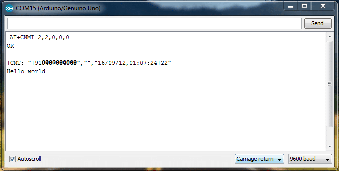 The ˇ°Hello worldˇ± is the message sent to GSM modem and the number from which the text message is sent also displayed.
Now, let send SMS to the pre-entered number in the program with pre-entered message.
Press ˇ°sˇ± and you will see something similar illustrated below: The sent SMS is ˇ°Hello I am GSM modemˇ±.
The ˇ°Hello worldˇ± is the message sent to GSM modem and the number from which the text message is sent also displayed.
Now, let send SMS to the pre-entered number in the program with pre-entered message.
Press ˇ°sˇ± and you will see something similar illustrated below: The sent SMS is ˇ°Hello I am GSM modemˇ±.
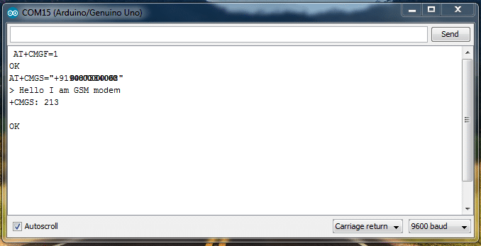 Now, you know how to send and how to receive SMS using GSM modem.
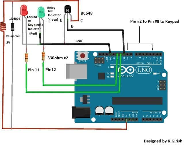 Here are the two illustrations how to interface keyboard and Arduino:
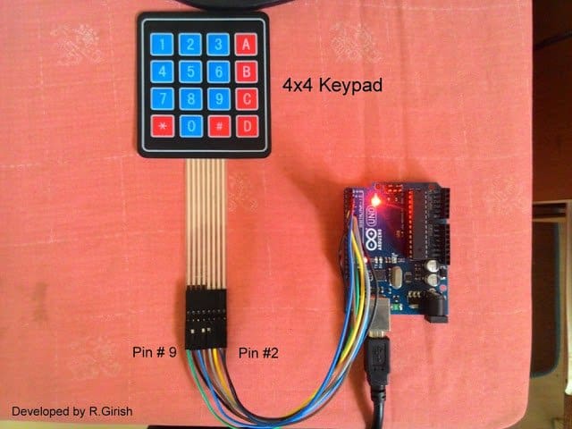
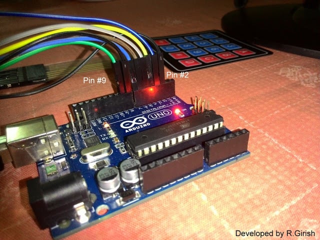 When the circuit is powered on, it asks for password, you can see on the serial monitor (serial monitor is not mandatory but, can be used for testing purpose).
Enter the password which you entered in the program before compiling it.
While you press the keys, green LED blinks for one tenth of a second, indicating that some key is pressed by the user.
Once you entered the 6-digit password, press ˇ®DˇŻ in the keypad which acts as ˇ®EnterˇŻ.
If your password is correct, the relay gets activated, green LED turns ON.
To deactivate the relay, press ˇ®CˇŻ in the keypad.
When, this is done, green LED turns OFF and relay gets deactivated.
No other key can deactivate the relay.
If the password enter by the user is incorrect, then red LED lights up and the user have to wait 30 second to enter the next attempt.
When the 30 second is over, the red LED turns OFF, informing the user that, the system ready to get input from the user.
When the relay is deactivated after successful activation, in order to activate the relay again, the user needs to enter the password again and press ˇ®DˇŻ.
Here is a special case:
When the correct password is entered, the relay gets activated and after the successful deactivation, when the user hits any one wrong keystroke (not whole password), the program recognize as incorrect password and the user need to wait another 30 second.
If this was a hijacker it will delay the number of attempt done by the hijacker.
When correct keystroke is pressed on the first attempt, only then it allows to enter next key.
This is only for first keystroke only and not for all the successive keystrokes.
The motto of the above explained concept is to delay the number of attempts done by the hijacker.
When the circuit is powered on, it asks for password, you can see on the serial monitor (serial monitor is not mandatory but, can be used for testing purpose).
Enter the password which you entered in the program before compiling it.
While you press the keys, green LED blinks for one tenth of a second, indicating that some key is pressed by the user.
Once you entered the 6-digit password, press ˇ®DˇŻ in the keypad which acts as ˇ®EnterˇŻ.
If your password is correct, the relay gets activated, green LED turns ON.
To deactivate the relay, press ˇ®CˇŻ in the keypad.
When, this is done, green LED turns OFF and relay gets deactivated.
No other key can deactivate the relay.
If the password enter by the user is incorrect, then red LED lights up and the user have to wait 30 second to enter the next attempt.
When the 30 second is over, the red LED turns OFF, informing the user that, the system ready to get input from the user.
When the relay is deactivated after successful activation, in order to activate the relay again, the user needs to enter the password again and press ˇ®DˇŻ.
Here is a special case:
When the correct password is entered, the relay gets activated and after the successful deactivation, when the user hits any one wrong keystroke (not whole password), the program recognize as incorrect password and the user need to wait another 30 second.
If this was a hijacker it will delay the number of attempt done by the hijacker.
When correct keystroke is pressed on the first attempt, only then it allows to enter next key.
This is only for first keystroke only and not for all the successive keystrokes.
The motto of the above explained concept is to delay the number of attempts done by the hijacker.
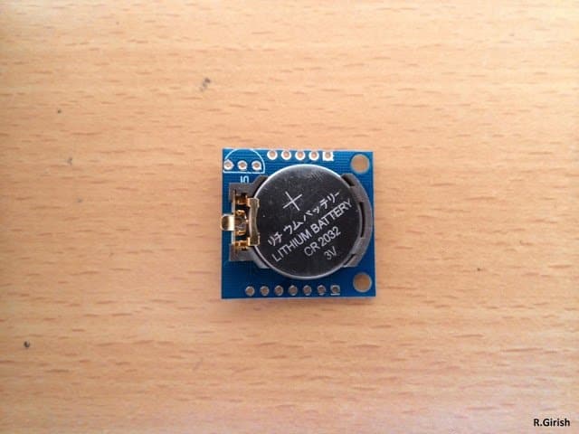
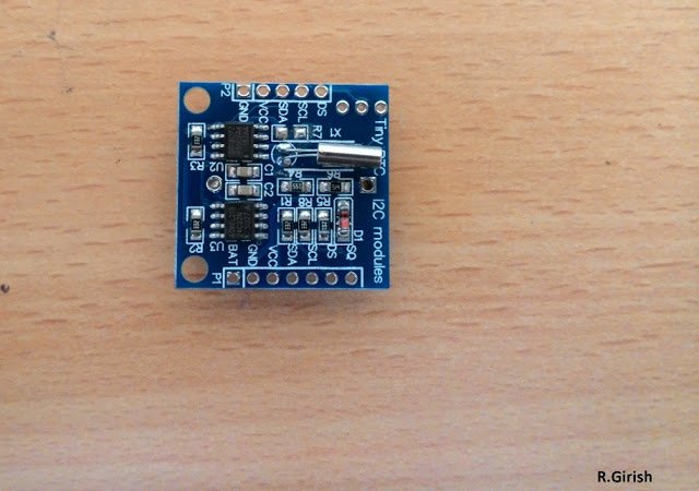 Most of the RTC modules come with battery (CR2032) at the time of purchase.
There are different of size and models, the above illustrated may not be the same for you.
But make sure the model number is DS1307. The code written in this post is only compatible with DS1307.
Now you know something about RTCs.
Now letˇŻs move on to the digital clock design.
Before proceeding with this project you need to download the library from the following links and install on your IDE:
DS1307RTC.h
Link: github.com/PaulStoffregen/DS1307RTC
TimeLib.h
Link: github.com/PaulStoffregen/Time
Other two libraries would have been preinstalled on Arduino IDE, if you are on latest version.
LiquidCrystal.h
Wire.h
Most of the RTC modules come with battery (CR2032) at the time of purchase.
There are different of size and models, the above illustrated may not be the same for you.
But make sure the model number is DS1307. The code written in this post is only compatible with DS1307.
Now you know something about RTCs.
Now letˇŻs move on to the digital clock design.
Before proceeding with this project you need to download the library from the following links and install on your IDE:
DS1307RTC.h
Link: github.com/PaulStoffregen/DS1307RTC
TimeLib.h
Link: github.com/PaulStoffregen/Time
Other two libraries would have been preinstalled on Arduino IDE, if you are on latest version.
LiquidCrystal.h
Wire.h
 The circuit connection between arduino and LCD display is standard, which we can find similar connection on other LCD based projects.
The only additional component is the RTC.
To reduce wire congestion during prototype, the RTC can be inserted to the analogue pins directly of the arduino.
Solder the SCl, SDA, Vcc, and GND with male header pins and insert it A2 to A5 pins as shown in the prototype.
AuthorˇŻs prototype:
The circuit connection between arduino and LCD display is standard, which we can find similar connection on other LCD based projects.
The only additional component is the RTC.
To reduce wire congestion during prototype, the RTC can be inserted to the analogue pins directly of the arduino.
Solder the SCl, SDA, Vcc, and GND with male header pins and insert it A2 to A5 pins as shown in the prototype.
AuthorˇŻs prototype:
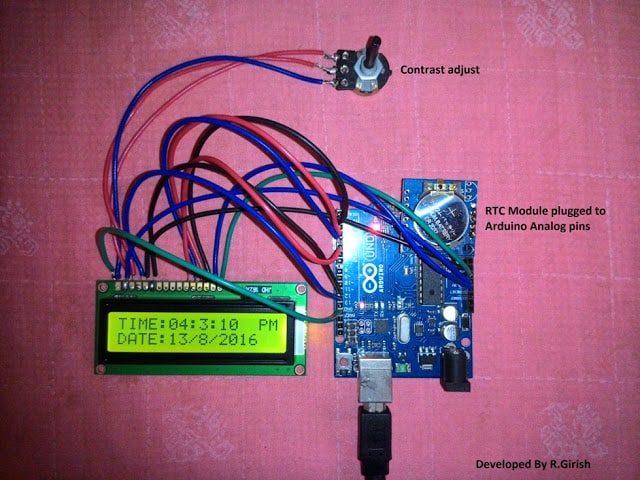
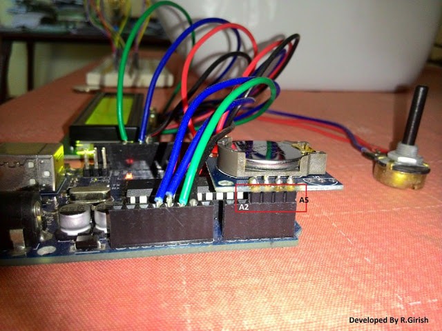 If your RTC has different pin locations and could not replicate as illustrated above, you can always use wires for connection.
Now your hardware setup is complete, letˇŻs move to the software part of the project.
If your RTC has different pin locations and could not replicate as illustrated above, you can always use wires for connection.
Now your hardware setup is complete, letˇŻs move to the software part of the project.
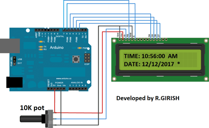 The above is the schematic is for Arduino to display connection, adjust the display contrast by rotating the 10K potentiometer.
The below is the rest of the circuit:
The circuit can be powered 9V 500mA wall adapter.
The above is the schematic is for Arduino to display connection, adjust the display contrast by rotating the 10K potentiometer.
The below is the rest of the circuit:
The circuit can be powered 9V 500mA wall adapter.

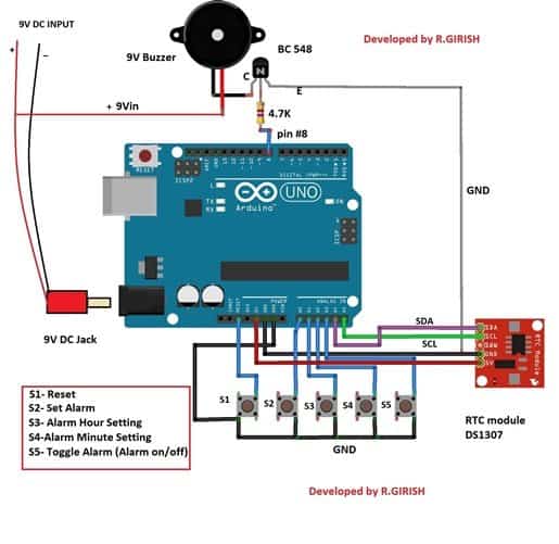

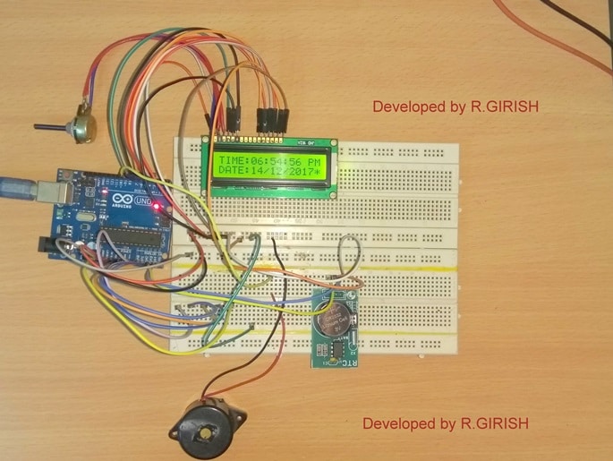 Do you like this project? Have any question regarding this project, feel free to express in the comment, you may receive a quick reply.
Video Clip:
Do you like this project? Have any question regarding this project, feel free to express in the comment, you may receive a quick reply.
Video Clip:
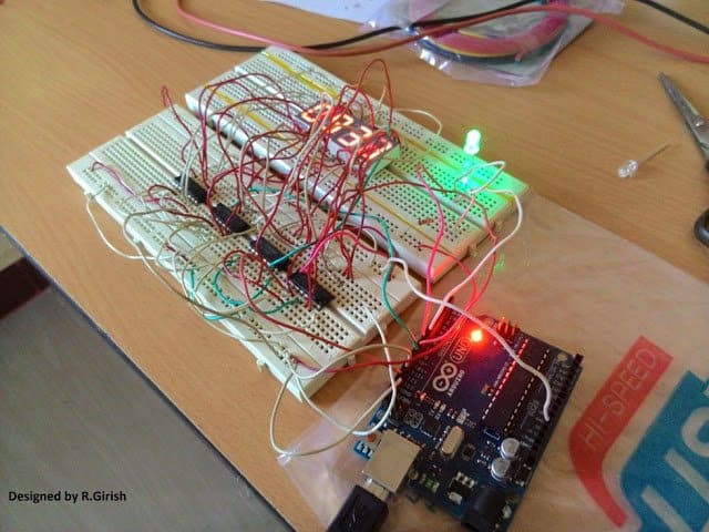 Here is a completed prototype using cardboard and scrap materials:

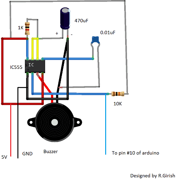
 Warning: You are advised to do extensive research on internet regarding the placement of electrode and the size of electrode.
 HereˇŻs how to make an electrode:
 The sponge must place on the skin not the metal part.
Please donˇŻt use any kind of metal electrode to contact with skin; it will cause small skin burn even at 1mA.
Do not use AC mains for power supply, small surge is enough to flow huge current on your head.
The sponge must place on the skin not the metal part.
Please donˇŻt use any kind of metal electrode to contact with skin; it will cause small skin burn even at 1mA.
Do not use AC mains for power supply, small surge is enough to flow huge current on your head.

 The biggest selling point of Raspberry Pi is price.
You can pick one for $35 or less than 2500 INR on E-commerce sites.
We are getting computing power equivalent to Pentium processors which was released on late 2000s.
But it consumes power 100 times less and sits on a single PCB, thanks to MoorˇŻs law.
After a huge success, Chinese electronic vendors started manufacturing similar single board computers, the popular ones are Banana Pi, Orange Pi, and Roseapple Pi etc; by the way the names can get ridiculous.
These single board computers function similar as raspberry Pi, but some has more functionality and some has less functionality than Raspberry Pi.
However Raspberry Pi has the most project support around world.
The biggest selling point of Raspberry Pi is price.
You can pick one for $35 or less than 2500 INR on E-commerce sites.
We are getting computing power equivalent to Pentium processors which was released on late 2000s.
But it consumes power 100 times less and sits on a single PCB, thanks to MoorˇŻs law.
After a huge success, Chinese electronic vendors started manufacturing similar single board computers, the popular ones are Banana Pi, Orange Pi, and Roseapple Pi etc; by the way the names can get ridiculous.
These single board computers function similar as raspberry Pi, but some has more functionality and some has less functionality than Raspberry Pi.
However Raspberry Pi has the most project support around world.


 I am using this NAS also as torrent file downloader (legally, LOL) for downloading huge files with minimum power, so that I do not need to run my main computer overnight, which could only raise the electricity bill.
As you can see, this small computer has huge potentials.
Once you get familiar with this single board computer you can do wonders.
I am using this NAS also as torrent file downloader (legally, LOL) for downloading huge files with minimum power, so that I do not need to run my main computer overnight, which could only raise the electricity bill.
As you can see, this small computer has huge potentials.
Once you get familiar with this single board computer you can do wonders.
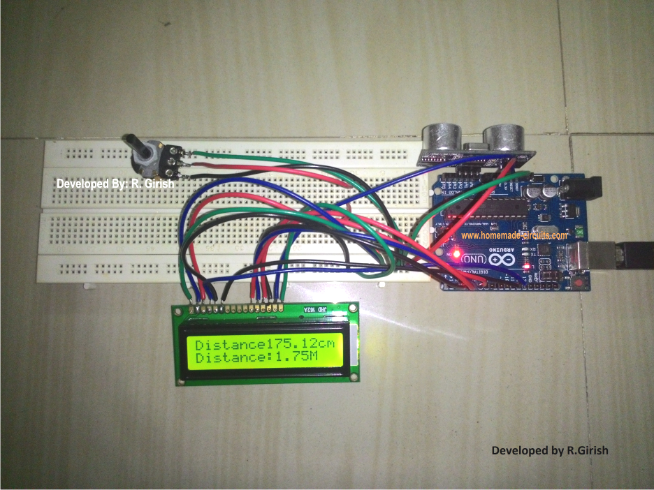
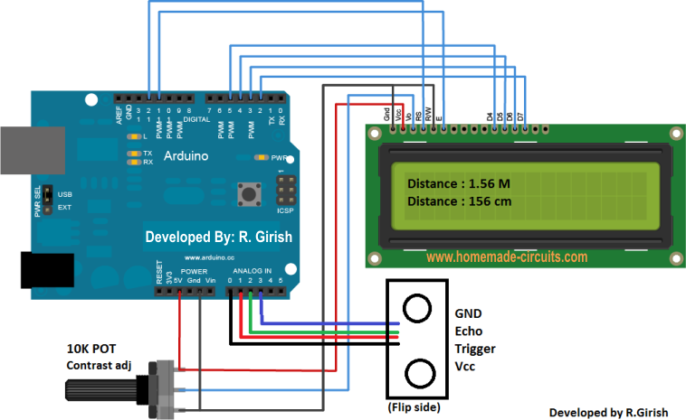 The ultrasonic distance meter circuit connection is done through a standard arduino-LCD interface, which we can also find on many other similar arduino-LCD based projects.
The potentiometer is used to adjust the contrast of LCD display.
The ultrasonic sensor can be directly inserted on analog pin as shown in authorˇŻs prototype from A0 to A3, sensors facing outwards; this may reduce wire congestion while duplicating the above circuit.
The ultrasonic distance meter circuit connection is done through a standard arduino-LCD interface, which we can also find on many other similar arduino-LCD based projects.
The potentiometer is used to adjust the contrast of LCD display.
The ultrasonic sensor can be directly inserted on analog pin as shown in authorˇŻs prototype from A0 to A3, sensors facing outwards; this may reduce wire congestion while duplicating the above circuit.
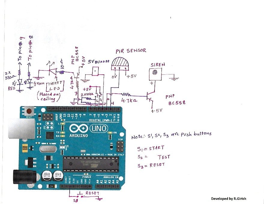 The home security system circuit using Arduino Uno is shown above, but you can use any of the arduino boards.
The circuit may look complicated but, actually not.
R3 is reset button is connected to Reset pin of the arduino and grounded.
All the transistors are PNP type.
If you want use NPN transistor, do the appropriate changes in the code.
There is 5v buzzer to give audio feed back to the user when any button is pressed.
Note: A pull down resistor 10K must be connected to #Pin 2 of the arduino, which is not shown in the schematic.
Direction for testing:
After completing the build and upload of the code, do the following instruction for testing.
ˇ¤ Power the circuit and press ˇ°testˇ± button; you will hear a beep and green LED on, indicating the circuit is ready for test mode and go away immediately from the circuit.
After 10 second youˇŻll here another beep, signifying the setup is ready to detect motion.
ˇ¤ Come near to the PIR sensor, immediately you will hear beep for 2 second along with 1 watt led ON.
Then it goes to idle state.
ˇ¤ If the above following instruction works, your security system is ready for use.
Do frequent testing to prolong working span of the system.
Direction for use: Understand the following instructions carefully.
ˇ¤ Lock the doors and press ˇ°Start buttonˇ± when gives double beep indicating you may leave now.
After 2 minutes it will give another double beep (by the time you wonˇŻt be present at home) indicating the system is active and ready to detect motion.
ˇ¤ If any motion is triggered by the intruder, firstly the 1 watt white led lights up and red LED also turns ON.
This is first stage to deter the crook.
The intruder may think someone is still left in the home.
ˇ¤ After 20 seconds the alarm starts, this is second stage for deter the crook.
The alarm will pull the attention of many near the area.
ˇ¤ After 1 minute the alarm stops 1 watt LED turns OFF but RED led stays on, indicating someone triggered the system.
ˇ¤ When owner of the house returns he will trigger the system, but it gives 20 second to deactivate the system by pressing ˇ°Resetˇ±.
By doing so it will go to idle mode.
If it was a crook he/she donˇŻt know the presence of security system and alarm triggered after 20 seconds.
The home security system circuit using Arduino Uno is shown above, but you can use any of the arduino boards.
The circuit may look complicated but, actually not.
R3 is reset button is connected to Reset pin of the arduino and grounded.
All the transistors are PNP type.
If you want use NPN transistor, do the appropriate changes in the code.
There is 5v buzzer to give audio feed back to the user when any button is pressed.
Note: A pull down resistor 10K must be connected to #Pin 2 of the arduino, which is not shown in the schematic.
Direction for testing:
After completing the build and upload of the code, do the following instruction for testing.
ˇ¤ Power the circuit and press ˇ°testˇ± button; you will hear a beep and green LED on, indicating the circuit is ready for test mode and go away immediately from the circuit.
After 10 second youˇŻll here another beep, signifying the setup is ready to detect motion.
ˇ¤ Come near to the PIR sensor, immediately you will hear beep for 2 second along with 1 watt led ON.
Then it goes to idle state.
ˇ¤ If the above following instruction works, your security system is ready for use.
Do frequent testing to prolong working span of the system.
Direction for use: Understand the following instructions carefully.
ˇ¤ Lock the doors and press ˇ°Start buttonˇ± when gives double beep indicating you may leave now.
After 2 minutes it will give another double beep (by the time you wonˇŻt be present at home) indicating the system is active and ready to detect motion.
ˇ¤ If any motion is triggered by the intruder, firstly the 1 watt white led lights up and red LED also turns ON.
This is first stage to deter the crook.
The intruder may think someone is still left in the home.
ˇ¤ After 20 seconds the alarm starts, this is second stage for deter the crook.
The alarm will pull the attention of many near the area.
ˇ¤ After 1 minute the alarm stops 1 watt LED turns OFF but RED led stays on, indicating someone triggered the system.
ˇ¤ When owner of the house returns he will trigger the system, but it gives 20 second to deactivate the system by pressing ˇ°Resetˇ±.
By doing so it will go to idle mode.
If it was a crook he/she donˇŻt know the presence of security system and alarm triggered after 20 seconds.
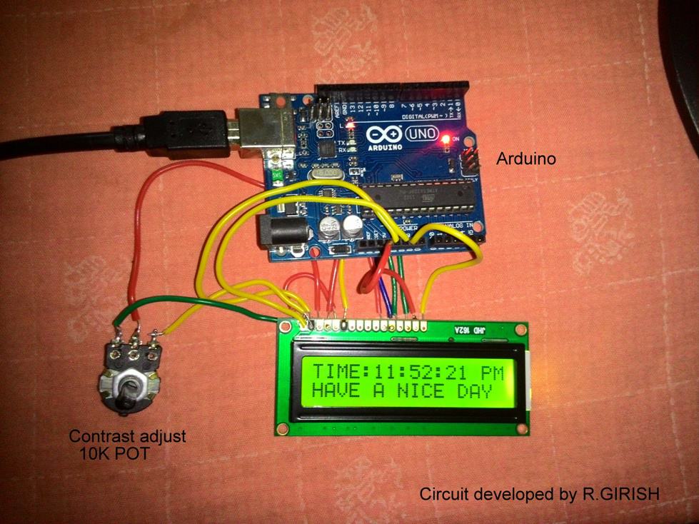 The LCD screen is a standard 16 pin interfaced display.
It has 16 rows and 2 columns, this means it can display 16 ASCII character in a row and it has two columns and thatˇŻs why it is called 16x2 display.
The wire connection between the LCD and Arduino is standard and we can find the similar kind of connections in most of the other Arduino-LCD based projects.
The potentiometer is used to adjust the contrast of the display.
The user must set this optimally so that the user can see the displayed digits/characters properly under all light situations.
There is backlight which enables the user to see the display during dark situation.
The arduino can be powered externally from DC jack from 7 volt to 12 volt.
The LCD screen is a standard 16 pin interfaced display.
It has 16 rows and 2 columns, this means it can display 16 ASCII character in a row and it has two columns and thatˇŻs why it is called 16x2 display.
The wire connection between the LCD and Arduino is standard and we can find the similar kind of connections in most of the other Arduino-LCD based projects.
The potentiometer is used to adjust the contrast of the display.
The user must set this optimally so that the user can see the displayed digits/characters properly under all light situations.
There is backlight which enables the user to see the display during dark situation.
The arduino can be powered externally from DC jack from 7 volt to 12 volt.
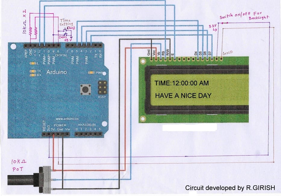
 Operating Voltage: 5V on USB and 7-12V on DC jack.
Digital I/O pins: 14 (6 of which can do PWM operations)
Analogue input pins: 6
Flash memory for storing program: 32KB
RAM: 2KB
EEPROM: 1KB
Clock Speed: 16MHz
DC output current per I/O pin: 20mA
Note: The above specification is only applicable for ATmega328P based arduino microcontroller.
Operating Voltage: 5V on USB and 7-12V on DC jack.
Digital I/O pins: 14 (6 of which can do PWM operations)
Analogue input pins: 6
Flash memory for storing program: 32KB
RAM: 2KB
EEPROM: 1KB
Clock Speed: 16MHz
DC output current per I/O pin: 20mA
Note: The above specification is only applicable for ATmega328P based arduino microcontroller.
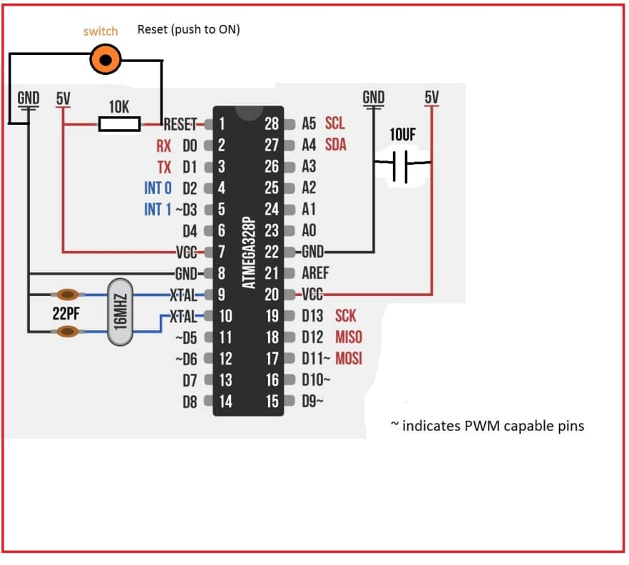 Once the project is complete you may pluck out ATmega328P and connect few external components as shown in diagram and you may solder it to PCB to make it permanent.
For your next project you no need to buy new arduino board, instead you may purchase the ATmega328P and few other external, which cost effective and make your project more compact.
Once the project is complete you may pluck out ATmega328P and connect few external components as shown in diagram and you may solder it to PCB to make it permanent.
For your next project you no need to buy new arduino board, instead you may purchase the ATmega328P and few other external, which cost effective and make your project more compact.
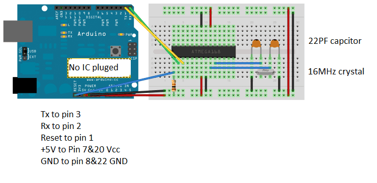 Select ˇ°Toolsˇ± > ˇ°Boardˇ±> ˇ°Arduino/Genuino UNOˇ±
Plug the arduino to your PC and select right port for your arduino (vary computer to computer.
Select ˇ°Toolsˇ±> ˇ°portˇ±).
Compile the program and click the upload button.
Select ˇ°Toolsˇ± > ˇ°Boardˇ±> ˇ°Arduino/Genuino UNOˇ±
Plug the arduino to your PC and select right port for your arduino (vary computer to computer.
Select ˇ°Toolsˇ±> ˇ°portˇ±).
Compile the program and click the upload button.

 An Arduino UNO board

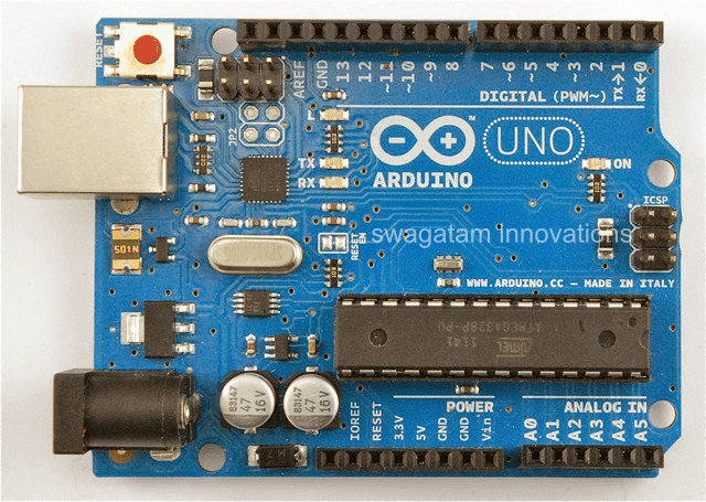 An Arduino USB cable
 Once you have acquired the above material and hooked them up with each other, it's just about configuring the following given sketch code into your Arduino board and watch the magic of the stop clock functions.

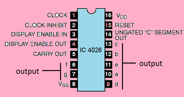 The pin #1 is clock input.
The pin #2 is clock disable, it disable the count on display if this pin is high.
The pin #3 is display enable; if this pin is low the display will be tuned off and vice versa.
The pin #5 is carry-out, which becomes high when IC counts 10.
The pins 6, 7, 9, 10, 11, 12, 13 are display outputs.
The pin #8 is GND.
The pin #16 is Vcc.
The pin #15 is reset, if we high this pin the count turns to zero.
The pins #4 and #14 are not used.
The pin #1 is clock input.
The pin #2 is clock disable, it disable the count on display if this pin is high.
The pin #3 is display enable; if this pin is low the display will be tuned off and vice versa.
The pin #5 is carry-out, which becomes high when IC counts 10.
The pins 6, 7, 9, 10, 11, 12, 13 are display outputs.
The pin #8 is GND.
The pin #16 is Vcc.
The pin #15 is reset, if we high this pin the count turns to zero.
The pins #4 and #14 are not used.

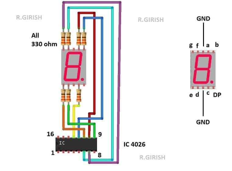 Any one of the GND pin of 7 segment display can be connected to ground.
The IC must be powered from 5V supply or ArduinoˇŻs 5V output pin.
The above schematic for just one display, repeat the same for five other displays.
Here is the rest of the schematic:
Any one of the GND pin of 7 segment display can be connected to ground.
The IC must be powered from 5V supply or ArduinoˇŻs 5V output pin.
The above schematic for just one display, repeat the same for five other displays.
Here is the rest of the schematic:

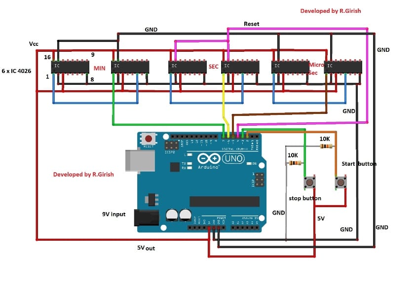 The circuit may be powered from 9V battery.
The are two buttons provided here one for starting the time and another for stopping.
By pressing reset button on Arduino, the time count will be reset to zero on display.
The two push button are connected to pin #2 and #3 which are hardware interrupt of Arduino / Atmega328P microcontroller.
The circuit may be powered from 9V battery.
The are two buttons provided here one for starting the time and another for stopping.
By pressing reset button on Arduino, the time count will be reset to zero on display.
The two push button are connected to pin #2 and #3 which are hardware interrupt of Arduino / Atmega328P microcontroller.
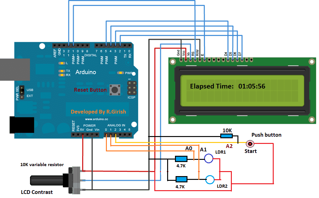 The interface between LCD and arduino is standard; we can find similar connection in many other LCD based projects.
Two analogue pins A0 and A1 are used to detect laser interruptions.
Analogue pin A2 is connected with push button which is used to arm the stopwatch.
Three resistors, two 4.7K and one 10K are pull-down down resistors which helps input pins to stay at low.
10K potentiometer is provided for adjusting contrast in LCD module for optimal visibility.
The proposed circuit has designed with fault detection mechanism for lasers.
If any one of the laser is fault or not aligned properly with LDR, it displays an error message on LCD display.
ˇ¤ If START laser is not functioning, it displays ˇ° ˇ®startˇŻ laser is not workingˇ±
ˇ¤ If STOP laser is not functioning, it displays ˇ° ˇ®stopˇŻ laser is not workingˇ±
ˇ¤ If both the lasers are not functioning, it displays ˇ°Both lasers are not workingˇ±
ˇ¤ If both the lasers are functioning properly, it displays ˇ°Both lasers are working fineˇ±
The error message appears until the laser module fixed or alignment is done properly with LDR.
Once this step is free of problem, the system goes to standby mode and displays ˇ°-system standby-ˇ°.
At this point the user can arm the setup by pressing the push button any time.
One the push button is pressed the system is ready to detect motion from the user and displays ˇ°System is readyˇ±.
The runner may be few inches from the ˇ®startˇŻ laser.
If the ˇ°startˇ± laser is interrupted the time begins to count and the displaysˇ± Time is being calculatedˇˇˇ± The time is calculated in the back ground.
The elapsed time wonˇŻt be displayed until the runner reaches/interrupts the ˇ°stopˇ± laser.
This is because displaying the elapsing time on LCD as traditional stopwatch does, require several additional instructions to be executed in the microcontroller, which deteriorates the accuracy of the setup significantly.
NOTE: Press reset button on arduino to clear the readings.
The interface between LCD and arduino is standard; we can find similar connection in many other LCD based projects.
Two analogue pins A0 and A1 are used to detect laser interruptions.
Analogue pin A2 is connected with push button which is used to arm the stopwatch.
Three resistors, two 4.7K and one 10K are pull-down down resistors which helps input pins to stay at low.
10K potentiometer is provided for adjusting contrast in LCD module for optimal visibility.
The proposed circuit has designed with fault detection mechanism for lasers.
If any one of the laser is fault or not aligned properly with LDR, it displays an error message on LCD display.
ˇ¤ If START laser is not functioning, it displays ˇ° ˇ®startˇŻ laser is not workingˇ±
ˇ¤ If STOP laser is not functioning, it displays ˇ° ˇ®stopˇŻ laser is not workingˇ±
ˇ¤ If both the lasers are not functioning, it displays ˇ°Both lasers are not workingˇ±
ˇ¤ If both the lasers are functioning properly, it displays ˇ°Both lasers are working fineˇ±
The error message appears until the laser module fixed or alignment is done properly with LDR.
Once this step is free of problem, the system goes to standby mode and displays ˇ°-system standby-ˇ°.
At this point the user can arm the setup by pressing the push button any time.
One the push button is pressed the system is ready to detect motion from the user and displays ˇ°System is readyˇ±.
The runner may be few inches from the ˇ®startˇŻ laser.
If the ˇ°startˇ± laser is interrupted the time begins to count and the displaysˇ± Time is being calculatedˇˇˇ± The time is calculated in the back ground.
The elapsed time wonˇŻt be displayed until the runner reaches/interrupts the ˇ°stopˇ± laser.
This is because displaying the elapsing time on LCD as traditional stopwatch does, require several additional instructions to be executed in the microcontroller, which deteriorates the accuracy of the setup significantly.
NOTE: Press reset button on arduino to clear the readings.
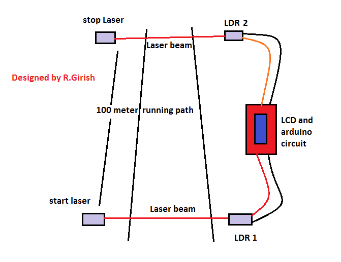 Please use thick wires to connect between LDRs and arduino circuit as the distance between these two may be several meters apart, and voltage must not drop significantly.
The distance between LDR1 and LDR2 can be few hundred meters maximum.
Please use thick wires to connect between LDRs and arduino circuit as the distance between these two may be several meters apart, and voltage must not drop significantly.
The distance between LDR1 and LDR2 can be few hundred meters maximum.
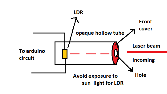 The LDR must be mounted inside hollow opaque tube and front part must also be covered and only a hole with few millimetres in diameter is made for allowing laser beam to enter in.
The LDR must be protected from direct sunlight as it cannot differentiate from laser beam and other source of light and might not register motion from the user.
The LDR must be mounted inside hollow opaque tube and front part must also be covered and only a hole with few millimetres in diameter is made for allowing laser beam to enter in.
The LDR must be protected from direct sunlight as it cannot differentiate from laser beam and other source of light and might not register motion from the user.
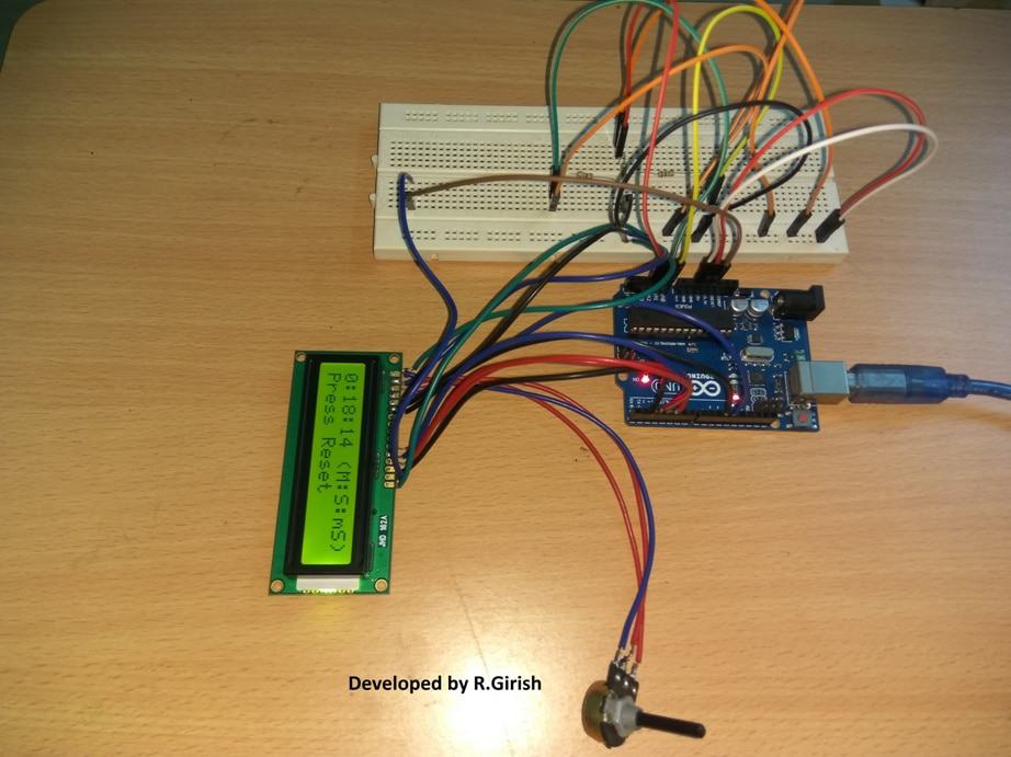
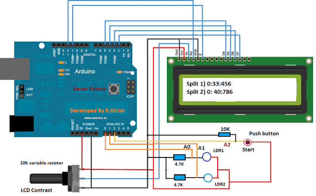 The above circuit consists of few components and beginner friendly.
No further explanation is required, just wire as per the circuit diagram.
The above circuit consists of few components and beginner friendly.
No further explanation is required, just wire as per the circuit diagram.
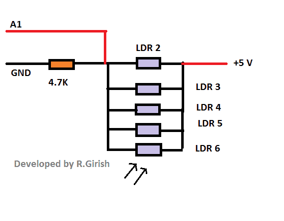 The LDR 2 is shown on the main circuit diagram; connect 4 more LDRs in parallel as shown in the above diagram.
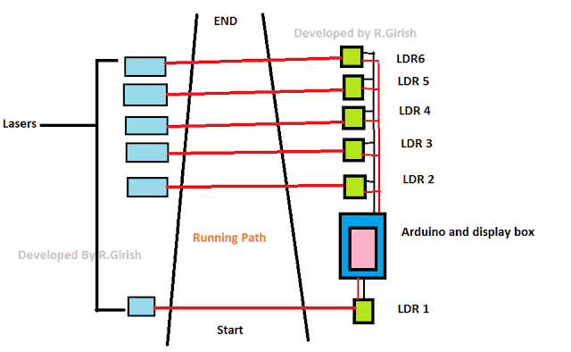 The above is the basic arrangement on how to place the laser.
Please note that the distance between LDRs can be choice of the user depending on track length.
The above is the basic arrangement on how to place the laser.
Please note that the distance between LDRs can be choice of the user depending on track length.

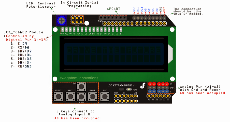
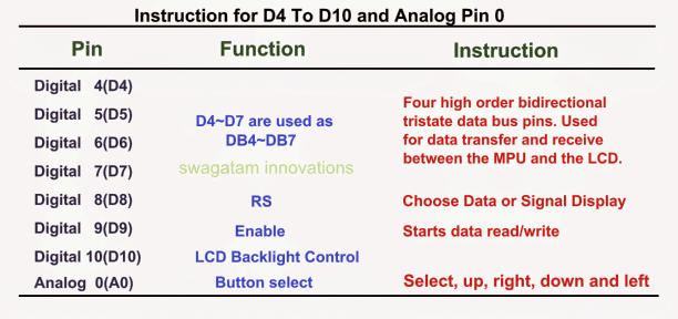
 The connection details of the proposed RGB LED sequential light circuit using Arduino can be seen in the above diagram.
The connections are pretty easy to implement, just insert the LED leads to the Arduino burg pinouts, switch the the power socket and visualize the RGB LED running the red, green, blue illuminating in a sequential manner.
The code is fully customizable as per the individual preferences and selections,
The connection details of the proposed RGB LED sequential light circuit using Arduino can be seen in the above diagram.
The connections are pretty easy to implement, just insert the LED leads to the Arduino burg pinouts, switch the the power socket and visualize the RGB LED running the red, green, blue illuminating in a sequential manner.
The code is fully customizable as per the individual preferences and selections,
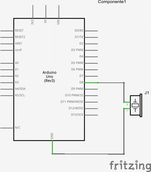
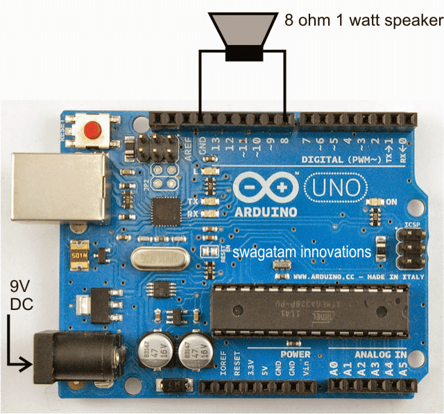 For high power amplified listening, the same set up can be upgraded with a power transistor as indicated in the following figure:
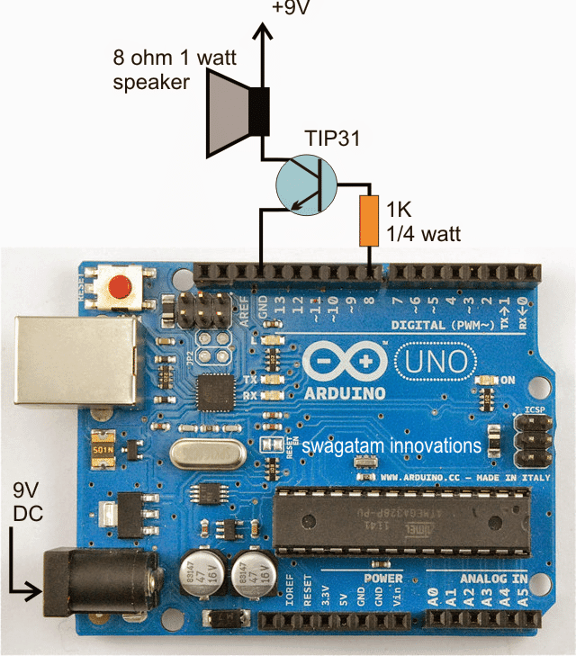
 Image Courtesy: https://arduino.cc/en/Tutorial/Tone
 The various pinouts of this advanced MCU unit may be understood from the folowing data:
Vcc = It's the Supply voltage pin of the IC compatible with digital IC supply voltage(5V)
GND refers to "ground" should be connected to the negative rail of the supply.
Port A (PA7...PA0): Here port A facilitates in the form of analogue inputs for the A/D converters.
This port may be also used as an 8-bit bi-directional Input/Output port, only when the A/D converter is excluded from being used.
Port pins are facilitated with in-built pull-up resistors (each bit being assigned).
The Port A buffered outputs also provide a well balanced and symmetrical drive characteristics inclusive of high sink and source capability.
When pins across PA0 and PA7 are assigned as inputs and are externally subjected to a logic low, they begin sourcing current as soon as the internal pull-up resistors get energized.
All the above discussed pinouts are tri-stated when the reset is triggered (even without the clocks being activated), tri-state refers to three types of conditions which the IC is able to produce: high, low, and non-responsive or open.
Port B (PB7...PB0): Basically, just like Port A, this Port also is an bi-directional 8 bit input/output port featured with internal pull-up resistors (configured for each bit).
The drive characteristics assigned to to Port B buffered pins are equipped with both high sinking and sourcing attributes.
When used as inputs, these pins source current when these are puled low by the external circuit stage due to the internal pull-up resistors being activated.
The Port B pins are also designated with a tri-state feature.
Apart from the above, Port B pins could be also used for implementing special features, as included in Atmega32, these are listed in the following table:
The various pinouts of this advanced MCU unit may be understood from the folowing data:
Vcc = It's the Supply voltage pin of the IC compatible with digital IC supply voltage(5V)
GND refers to "ground" should be connected to the negative rail of the supply.
Port A (PA7...PA0): Here port A facilitates in the form of analogue inputs for the A/D converters.
This port may be also used as an 8-bit bi-directional Input/Output port, only when the A/D converter is excluded from being used.
Port pins are facilitated with in-built pull-up resistors (each bit being assigned).
The Port A buffered outputs also provide a well balanced and symmetrical drive characteristics inclusive of high sink and source capability.
When pins across PA0 and PA7 are assigned as inputs and are externally subjected to a logic low, they begin sourcing current as soon as the internal pull-up resistors get energized.
All the above discussed pinouts are tri-stated when the reset is triggered (even without the clocks being activated), tri-state refers to three types of conditions which the IC is able to produce: high, low, and non-responsive or open.
Port B (PB7...PB0): Basically, just like Port A, this Port also is an bi-directional 8 bit input/output port featured with internal pull-up resistors (configured for each bit).
The drive characteristics assigned to to Port B buffered pins are equipped with both high sinking and sourcing attributes.
When used as inputs, these pins source current when these are puled low by the external circuit stage due to the internal pull-up resistors being activated.
The Port B pins are also designated with a tri-state feature.
Apart from the above, Port B pins could be also used for implementing special features, as included in Atmega32, these are listed in the following table:
 Port C (PC7...PC0): Port C pinouts also enjoy the various characteristics features enabled for the Port A and Port B.
However, apart from the identical features of port A and B, the internal pull-up resistor for Port C pins PC5(TDI), PC3(TMS) and PC2(TCK) all become activated even during a reset action in case when JTAG interface is toggled.
Additionally Port C also carries out the function of JTAG interface and other specified features of ATmega32 as shown in the below table:
Port C (PC7...PC0): Port C pinouts also enjoy the various characteristics features enabled for the Port A and Port B.
However, apart from the identical features of port A and B, the internal pull-up resistor for Port C pins PC5(TDI), PC3(TMS) and PC2(TCK) all become activated even during a reset action in case when JTAG interface is toggled.
Additionally Port C also carries out the function of JTAG interface and other specified features of ATmega32 as shown in the below table:
 Port D (PD7..PD0): Again just like the above ports, the fundamental current sinking and sourcing characteristics of Port D is exactly the same.
However when used alternately these pins may be used for enforcing special ATmega32 functions which may be studied through the following table:
Port D (PD7..PD0): Again just like the above ports, the fundamental current sinking and sourcing characteristics of Port D is exactly the same.
However when used alternately these pins may be used for enforcing special ATmega32 functions which may be studied through the following table:
 RESET: As the name suggests, the reset pinout may be used for resetting or forcing the IC to resume its functioning may be simply done by applying a low logic pulse here, however the minimum length of this pulse must not be less the specified pulse length of the IC.
Anything shorter than this may not guarantee a reset action.
The following table indicates the minimum reset pulse length applicable:
RESET: As the name suggests, the reset pinout may be used for resetting or forcing the IC to resume its functioning may be simply done by applying a low logic pulse here, however the minimum length of this pulse must not be less the specified pulse length of the IC.
Anything shorter than this may not guarantee a reset action.
The following table indicates the minimum reset pulse length applicable:
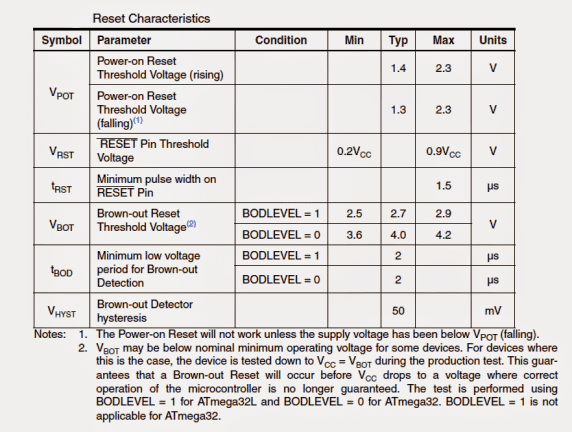 XTAL1: May be used for latching on to a given frequency and for enabling a flawless frequency response across the input pin of the inverting amplifier and input of the internal clock producing circuit.
XTAL2: Just as above this may be configured across output pinout of the inverting oscillator amplifier
AREF: It refers to the analogue reference pinout assigned for the internal A/D converter stage
XTAL1: May be used for latching on to a given frequency and for enabling a flawless frequency response across the input pin of the inverting amplifier and input of the internal clock producing circuit.
XTAL2: Just as above this may be configured across output pinout of the inverting oscillator amplifier
AREF: It refers to the analogue reference pinout assigned for the internal A/D converter stage
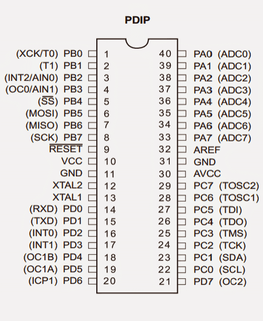 When it comes to MCUs, you get the facility of having the option of controlling and configuring all of its pinouts.
If you are getting a bit tired with this, just chill cause it's nothing complex at all, you will be eased through all the aspects steadily but firmly as we move ahead.
In an MCU chip all pins except the Vdd and Vss which are the power pins of the chip, can be assigned with exclusive designations.
When it comes to MCUs, you get the facility of having the option of controlling and configuring all of its pinouts.
If you are getting a bit tired with this, just chill cause it's nothing complex at all, you will be eased through all the aspects steadily but firmly as we move ahead.
In an MCU chip all pins except the Vdd and Vss which are the power pins of the chip, can be assigned with exclusive designations.
 It may be observed that quite a few of these programmers employ identical drivers, something tat must be taken care of and weˇŻll learn more about it in our subsequent chapters.
Connecting your PC with the microcontroller chip is truly basic, and you would be delighted to know how simple the proceedings are required for this.
So letˇŻs hit the button right awayJ
Making the above explained SPI interface board is not difficult, itˇŻs all about getting your solder iron working through all the connections across the shown two header rows of pins on a small general purpose board.
The figure above shows the connection details that you would have to follow while interconnecting the wires between the headers.
To make things even simpler, letˇŻs go through the following connection details for the same by referring to the image above:
SPI pin starting from top left goes to the ˇ°Master IN, Slave OUTˇ± (MISO)
SPI pin from center left connects with the clock pin (SCK)
SPI pin at the bottom left joins with the Reset.
(WeˇŻll learn elaborately about this pin in the following tutorials)
SPI relevant to bottom right hooks up with the GND pin of the MCU, GND refers to the pin which forms the zero supply line or the negative (relative) rail of the supply.
SPI terminating from middle right header links up with ˇ°Master Out, Slave INˇ± (MOSI) pin of the MCU.
SPI coming out of the top right header is wired up with the (+) of the MCU which is quite obviously the Vdd or the positive supply pin of the MCU.
It may be observed that quite a few of these programmers employ identical drivers, something tat must be taken care of and weˇŻll learn more about it in our subsequent chapters.
Connecting your PC with the microcontroller chip is truly basic, and you would be delighted to know how simple the proceedings are required for this.
So letˇŻs hit the button right awayJ
Making the above explained SPI interface board is not difficult, itˇŻs all about getting your solder iron working through all the connections across the shown two header rows of pins on a small general purpose board.
The figure above shows the connection details that you would have to follow while interconnecting the wires between the headers.
To make things even simpler, letˇŻs go through the following connection details for the same by referring to the image above:
SPI pin starting from top left goes to the ˇ°Master IN, Slave OUTˇ± (MISO)
SPI pin from center left connects with the clock pin (SCK)
SPI pin at the bottom left joins with the Reset.
(WeˇŻll learn elaborately about this pin in the following tutorials)
SPI relevant to bottom right hooks up with the GND pin of the MCU, GND refers to the pin which forms the zero supply line or the negative (relative) rail of the supply.
SPI terminating from middle right header links up with ˇ°Master Out, Slave INˇ± (MOSI) pin of the MCU.
SPI coming out of the top right header is wired up with the (+) of the MCU which is quite obviously the Vdd or the positive supply pin of the MCU.
 ThatˇŻs it.
Connect the two connectors as explained and your SPI interface board is ready for the required actions.
For further help you may consult the figure that shown above, your final interface board should look like this after all the wire connections are appropriately done with the help of the above discussion.
I hope you might have already constructed the SPI interface as explained in the previous tutorial, and now itˇŻs time to ensure that our computer accepts the programmer that we need to integrate in between the PC and the MCU.
ThatˇŻs it.
Connect the two connectors as explained and your SPI interface board is ready for the required actions.
For further help you may consult the figure that shown above, your final interface board should look like this after all the wire connections are appropriately done with the help of the above discussion.
I hope you might have already constructed the SPI interface as explained in the previous tutorial, and now itˇŻs time to ensure that our computer accepts the programmer that we need to integrate in between the PC and the MCU.
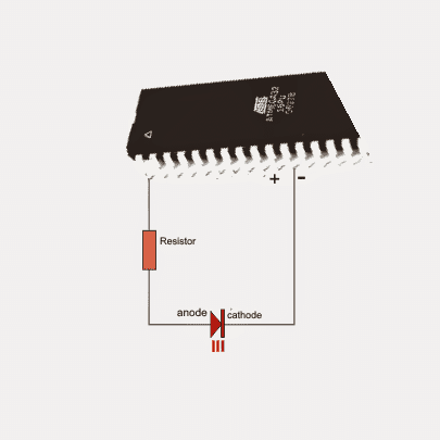 The value of the resistor may be calculated by using the following simple formula:
R = (Ub ¨C LEDfwd)/I
Where Ub is the supply voltage, LEDfwd is the optimal operating voltage of the LED used, and I is its optimal amps.
Suppose we use a RED LED which has a LED forward voltage = 2.5V and current I = 20mA, the above equation can be solved as follows:
Since the voltage from MCU would be 5V, it may be expressed as:
R = (5 ¨C 2.5)/.02 = 125 ohms, watt, the nearest value being 120 ohms will do.
Now we have the LED, a 120 ohm resistor and a veroboard, simply interconnect the above components as given in the diagram with the microcontroller.
Once this is done, the MCU could be programmed for the intended response on the above LED set up.
Next up, the programming of the MCU.
In order to allow the microcontroller to perform some meaningful implementations, itˇŻs imperative to write appropriate instructions into the MCU.
The value of the resistor may be calculated by using the following simple formula:
R = (Ub ¨C LEDfwd)/I
Where Ub is the supply voltage, LEDfwd is the optimal operating voltage of the LED used, and I is its optimal amps.
Suppose we use a RED LED which has a LED forward voltage = 2.5V and current I = 20mA, the above equation can be solved as follows:
Since the voltage from MCU would be 5V, it may be expressed as:
R = (5 ¨C 2.5)/.02 = 125 ohms, watt, the nearest value being 120 ohms will do.
Now we have the LED, a 120 ohm resistor and a veroboard, simply interconnect the above components as given in the diagram with the microcontroller.
Once this is done, the MCU could be programmed for the intended response on the above LED set up.
Next up, the programming of the MCU.
In order to allow the microcontroller to perform some meaningful implementations, itˇŻs imperative to write appropriate instructions into the MCU.
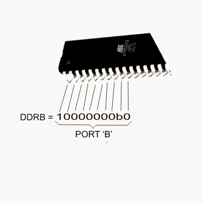 Finally in the previous chapter we finished building the LED/ resistor circuit and connected it with the relevant MCU outputs.
ThatˇŻs a lot of work indeed; nevertheless itˇŻs time to head right away into some real programming stuff!
To begin with we would want to divide the microcontroller into three categories; this would simplify our understanding a lot:
Control, Detection, and Communication
It would be interesting know that the above functions could be programmed in many different ways.
In our first program we would try to order the microcontroller to ˇ°controlˇ± an external parameter, yes you are right it would be the LED that we built recently.
To be precise, weˇŻll tell the MCU to switch ON the connected LED, yep I know this looks quite primitive, but the starting phase always needs to be easy.
Moving ahead with the present job, making the MCU control the LED is actually pretty simple:
For this we instruct pin#0 on PORT B to produce the required 5V for the LED.
Recall from the previous tutorial, we connected the anode of the LED to the above mentioned pin of the MCU.
There are two essential things required to be addressed to this pin of the MCU: 1) output and 2) 5 volts
WeˇŻll learn a way through which we ca instruct the particular pin to become the output of the MCU.
Once itˇŻs set to be the output of the chip, we may instruct it to be either ˇ°highˇ± (5V) or ˇ°lowˇ± (0V) as desired for an application.
Since the any logic circuit such as a MCU the pins could be wither an output or an input and could be configured to produce either a logic high or logic low, the pins only need to be assigned either to be a logical high or a logical low, there arenˇŻt any intermediate or undefined states other than these couple of states for microcontrollers or for any digital IC for that matter.
Also the same applies for each and every pin of the MCU.
As for the input and output pin assignments, the inputs would be positioned to accept signals from external analogue stages, while the outputs would be responsible for interpreting these into the specified logical states, or a frequency.
Although the above assignments could be done in many different methods, we would be discussing one of them for the sake of simplicity.
However it must be noted that although the one which would presented right now looks easy and interesting, itˇŻs not so viable and not a recommended type for all MCU applications, for the same reason you would be introduced to more popular programming methods later in the course.
These programs will allow only the desired pins to be assigned as per the specs without affecting the other adjoining which could be possibly already assigned to do some other functions.
However right now we wonˇŻt be bothering about the other pins so much and would use only the relevant pins of interest, avoiding complications to some extents.
For assigning a pin as an output we need to employ the Data Direction Register (DDR).
If you are wondering what register here means, itˇŻs simply a space in the MCU that enables the microcontroller to respond in some specified manner.
Using the DDR we can set the pin to either send a data that is like an ˇ°outputˇ±, or accept data that is in the form of an ˇ°inputˇ±.
However you may be confused regarding the word, what does this imply? A data adds a third dimension to the pins which may be assigned to be continuously at logic zero (0V) or logic high (5V), but what about the signals which could vary quickly such as a frequency of pulses.
A frequency would be accompanied with high and low logics (5V and 0V) oscillating with some specified intervals or periods, thus it becomes time oriented and may be adjusted with respect to time, thatˇŻs why we identify as ˇ°dataˇ± meaning a parameter which indicates a function relative to another function (logic states and time).
One method of assigning pin0 as an output is by writing the following code:
DDRB = 0b00000001;
In the above program, DDRB signifies Data Direction Register for PORT B; 0b instructs the compiler regarding the following binary expression of a number; while the ˇ°1ˇ± at the end of the expression indicates the position of the pin0, that is itˇŻs location in the form of the first pin of PORT B.
If you remember we learned that PORT B associates 8 pins with it (from 0 to pin7), and if you notice the above code also has 8 digits in it, meaning each digit signifies these 8 pins of PORT B.
Now the next procedure would be to assign 5V to this pin (pin0).
Again the principle of operation is identical to DDR as above expressed through the following binary code:
PORTB = 0b00000001;
As can be seen, the only difference between the above code and the earlier one is that in this code we have made use of the PORT register.
This register specifically handles the pin assignments of that particular port for which itˇŻs been positioned inside te MCU.
Thus it enables us to assign the real data logics (0 or 1) for those pinouts.
Now we may be interested to discuss some regarding the approximate details of our program.
As we know all programs require a particular space to initiate the execution, this can be compared to a chef who knows all the ingredients regarding a particular recipe but is not instructed from where to begin.
The ˇ°mainˇ± function here is the location where each of the C/C++ programs initiates the execution.
Therefore the main may be created as:
int main(void)
{
}
However to enable the program to interpret the DDR and PORT register details and their functioning inside the MCU chip, an additional statement needs to be included which may consist of all the data regarding the AVR MCU.
Perhaps we would want to add this inclusion in all of our programs.
#include <avr/io.h>
int main(void)
{
}
As soon as the compilation initiates, the pre-processor section of the compiler focuses on the AVR directory to identify the ˇ°io.hˇ± file.
The extension ˇ°.hˇ± here indicates it to be a header file, and that this code inside the file would be introduced at the start (head) of the source file thatˇŻs being created, hence the name ˇ°headerˇ±.
Here on we can introduce the DDR and PORT statements into our code, because the addition of the io.h header file would have directed the compiler regarding them.
#include <avr/io.h>
int main(void)
{
DDRB = 0b00000001; //Data Direction Register setting pin0 to output and the remaining pins as input
PORTB = 0b00000001; //Set pin0 to 5 volts
}
The above fixes the orientation of the pin0 as the output, having a magnitude of 5V.
However thereˇŻs still one issue which isnˇŻt determined for this pin, that is this pin is yet to be instructed to be switched ON indefinitely as long as the MCU is powered.
This infinite feedback loop would ensure that this pin from the MCU does not switch OFF, rather continues with the 5V output indefinitely.
Although there are many different methods of applying a loop instruction for a pin, we would try employing the ˇ°whileˇ± loop here.
As the name suggest, the ˇ°whileˇ± loop tells the microcontroller that ˇ°whileˇ± the power is available you need to stay activated with the assigned 5V for the assigned pinout.
#include <avr/io.h>
int main(void)
{
DDRB = 0b00000001; //Data Direction Register setting pin0 to output and the remaining pins as input
PORTB = 0b00000001; //Set pin0 to 5 volts
while(1)
{
//Code would be in here if it needed to execute over and over and over ...
endlessly
}
}
You might want to note that, here we have used ˇ®1ˇŻ in the form of an argument for the ˇ°whileˇ± loop, since everything except ˇ®0ˇŻ could be considered a logical ˇ°trueˇ±.
That implies, the ˇ°whileˇ± loop consideration would never be responsible for anything except a logical ˇ°trueˇ±, which means that the particular pin would latch on with the specified state indefinitely.
Finally in the previous chapter we finished building the LED/ resistor circuit and connected it with the relevant MCU outputs.
ThatˇŻs a lot of work indeed; nevertheless itˇŻs time to head right away into some real programming stuff!
To begin with we would want to divide the microcontroller into three categories; this would simplify our understanding a lot:
Control, Detection, and Communication
It would be interesting know that the above functions could be programmed in many different ways.
In our first program we would try to order the microcontroller to ˇ°controlˇ± an external parameter, yes you are right it would be the LED that we built recently.
To be precise, weˇŻll tell the MCU to switch ON the connected LED, yep I know this looks quite primitive, but the starting phase always needs to be easy.
Moving ahead with the present job, making the MCU control the LED is actually pretty simple:
For this we instruct pin#0 on PORT B to produce the required 5V for the LED.
Recall from the previous tutorial, we connected the anode of the LED to the above mentioned pin of the MCU.
There are two essential things required to be addressed to this pin of the MCU: 1) output and 2) 5 volts
WeˇŻll learn a way through which we ca instruct the particular pin to become the output of the MCU.
Once itˇŻs set to be the output of the chip, we may instruct it to be either ˇ°highˇ± (5V) or ˇ°lowˇ± (0V) as desired for an application.
Since the any logic circuit such as a MCU the pins could be wither an output or an input and could be configured to produce either a logic high or logic low, the pins only need to be assigned either to be a logical high or a logical low, there arenˇŻt any intermediate or undefined states other than these couple of states for microcontrollers or for any digital IC for that matter.
Also the same applies for each and every pin of the MCU.
As for the input and output pin assignments, the inputs would be positioned to accept signals from external analogue stages, while the outputs would be responsible for interpreting these into the specified logical states, or a frequency.
Although the above assignments could be done in many different methods, we would be discussing one of them for the sake of simplicity.
However it must be noted that although the one which would presented right now looks easy and interesting, itˇŻs not so viable and not a recommended type for all MCU applications, for the same reason you would be introduced to more popular programming methods later in the course.
These programs will allow only the desired pins to be assigned as per the specs without affecting the other adjoining which could be possibly already assigned to do some other functions.
However right now we wonˇŻt be bothering about the other pins so much and would use only the relevant pins of interest, avoiding complications to some extents.
For assigning a pin as an output we need to employ the Data Direction Register (DDR).
If you are wondering what register here means, itˇŻs simply a space in the MCU that enables the microcontroller to respond in some specified manner.
Using the DDR we can set the pin to either send a data that is like an ˇ°outputˇ±, or accept data that is in the form of an ˇ°inputˇ±.
However you may be confused regarding the word, what does this imply? A data adds a third dimension to the pins which may be assigned to be continuously at logic zero (0V) or logic high (5V), but what about the signals which could vary quickly such as a frequency of pulses.
A frequency would be accompanied with high and low logics (5V and 0V) oscillating with some specified intervals or periods, thus it becomes time oriented and may be adjusted with respect to time, thatˇŻs why we identify as ˇ°dataˇ± meaning a parameter which indicates a function relative to another function (logic states and time).
One method of assigning pin0 as an output is by writing the following code:
DDRB = 0b00000001;
In the above program, DDRB signifies Data Direction Register for PORT B; 0b instructs the compiler regarding the following binary expression of a number; while the ˇ°1ˇ± at the end of the expression indicates the position of the pin0, that is itˇŻs location in the form of the first pin of PORT B.
If you remember we learned that PORT B associates 8 pins with it (from 0 to pin7), and if you notice the above code also has 8 digits in it, meaning each digit signifies these 8 pins of PORT B.
Now the next procedure would be to assign 5V to this pin (pin0).
Again the principle of operation is identical to DDR as above expressed through the following binary code:
PORTB = 0b00000001;
As can be seen, the only difference between the above code and the earlier one is that in this code we have made use of the PORT register.
This register specifically handles the pin assignments of that particular port for which itˇŻs been positioned inside te MCU.
Thus it enables us to assign the real data logics (0 or 1) for those pinouts.
Now we may be interested to discuss some regarding the approximate details of our program.
As we know all programs require a particular space to initiate the execution, this can be compared to a chef who knows all the ingredients regarding a particular recipe but is not instructed from where to begin.
The ˇ°mainˇ± function here is the location where each of the C/C++ programs initiates the execution.
Therefore the main may be created as:
int main(void)
{
}
However to enable the program to interpret the DDR and PORT register details and their functioning inside the MCU chip, an additional statement needs to be included which may consist of all the data regarding the AVR MCU.
Perhaps we would want to add this inclusion in all of our programs.
#include <avr/io.h>
int main(void)
{
}
As soon as the compilation initiates, the pre-processor section of the compiler focuses on the AVR directory to identify the ˇ°io.hˇ± file.
The extension ˇ°.hˇ± here indicates it to be a header file, and that this code inside the file would be introduced at the start (head) of the source file thatˇŻs being created, hence the name ˇ°headerˇ±.
Here on we can introduce the DDR and PORT statements into our code, because the addition of the io.h header file would have directed the compiler regarding them.
#include <avr/io.h>
int main(void)
{
DDRB = 0b00000001; //Data Direction Register setting pin0 to output and the remaining pins as input
PORTB = 0b00000001; //Set pin0 to 5 volts
}
The above fixes the orientation of the pin0 as the output, having a magnitude of 5V.
However thereˇŻs still one issue which isnˇŻt determined for this pin, that is this pin is yet to be instructed to be switched ON indefinitely as long as the MCU is powered.
This infinite feedback loop would ensure that this pin from the MCU does not switch OFF, rather continues with the 5V output indefinitely.
Although there are many different methods of applying a loop instruction for a pin, we would try employing the ˇ°whileˇ± loop here.
As the name suggest, the ˇ°whileˇ± loop tells the microcontroller that ˇ°whileˇ± the power is available you need to stay activated with the assigned 5V for the assigned pinout.
#include <avr/io.h>
int main(void)
{
DDRB = 0b00000001; //Data Direction Register setting pin0 to output and the remaining pins as input
PORTB = 0b00000001; //Set pin0 to 5 volts
while(1)
{
//Code would be in here if it needed to execute over and over and over ...
endlessly
}
}
You might want to note that, here we have used ˇ®1ˇŻ in the form of an argument for the ˇ°whileˇ± loop, since everything except ˇ®0ˇŻ could be considered a logical ˇ°trueˇ±.
That implies, the ˇ°whileˇ± loop consideration would never be responsible for anything except a logical ˇ°trueˇ±, which means that the particular pin would latch on with the specified state indefinitely.
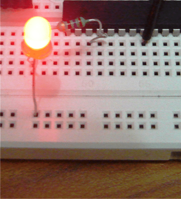

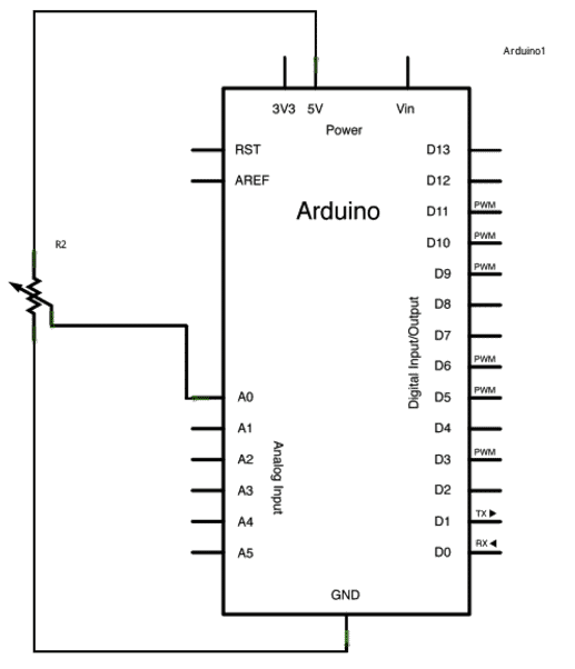 In the referred program the setup function solely needs to be triggered for initiating serial communications, the rate being 9600 bits of data per second, across your Arduino board and the computer.
The expected command is in the form:
Serial.begin(9600);
Subsequently, in the main loop of your code, we enforce a variable in order to fix the resistance value (which would be as discussed between 0 and 1023, just suitable for an int data type) received from the pot leads:
int sensorValue = analogRead(A0);
To conclude, print this information to your serial window as a decimal (DEC) value.
You can use the command Serial.println() for implementing this in the last line of code:
Serial.println(sensorValue, DEC)
After this, whenever Serial Monitor is initiated in the Arduino development domain (this is done by clicking the button that's immediately at the right hand side of the "Upload" button in the header of the program).
we would see a consistent chain of digits running from 0-1023, corresponding to the varying rotational position of the pot shaft.
If we stop the rotation of the pot shaft at some instant, the corresponding instantaneous number will get displayed on the screen of the Arduino, this would again change proportionately as we go on changing the pot shaft position.
The Code
/*
AnalogReadSerial
Reads an analog input on pin 0, prints the result to the serial monitor.
Attach the center pin of a potentiometer to pin A0, and the outside pins to +5V and ground.
This example code is in the public domain.
*/
// the setup routine runs once when you press reset:
void setup() {
// initialize serial communication at 9600 bits per second:
Serial.begin(9600);
}
// the loop routine runs over and over again forever:
void loop() {
// read the input on analog pin 0:
int sensorValue = analogRead(A0);
// print out the value you read:
Serial.println(sensorValue);
delay(1); // delay in between reads for stability
}
In the referred program the setup function solely needs to be triggered for initiating serial communications, the rate being 9600 bits of data per second, across your Arduino board and the computer.
The expected command is in the form:
Serial.begin(9600);
Subsequently, in the main loop of your code, we enforce a variable in order to fix the resistance value (which would be as discussed between 0 and 1023, just suitable for an int data type) received from the pot leads:
int sensorValue = analogRead(A0);
To conclude, print this information to your serial window as a decimal (DEC) value.
You can use the command Serial.println() for implementing this in the last line of code:
Serial.println(sensorValue, DEC)
After this, whenever Serial Monitor is initiated in the Arduino development domain (this is done by clicking the button that's immediately at the right hand side of the "Upload" button in the header of the program).
we would see a consistent chain of digits running from 0-1023, corresponding to the varying rotational position of the pot shaft.
If we stop the rotation of the pot shaft at some instant, the corresponding instantaneous number will get displayed on the screen of the Arduino, this would again change proportionately as we go on changing the pot shaft position.
The Code
/*
AnalogReadSerial
Reads an analog input on pin 0, prints the result to the serial monitor.
Attach the center pin of a potentiometer to pin A0, and the outside pins to +5V and ground.
This example code is in the public domain.
*/
// the setup routine runs once when you press reset:
void setup() {
// initialize serial communication at 9600 bits per second:
Serial.begin(9600);
}
// the loop routine runs over and over again forever:
void loop() {
// read the input on analog pin 0:
int sensorValue = analogRead(A0);
// print out the value you read:
Serial.println(sensorValue);
delay(1); // delay in between reads for stability
}
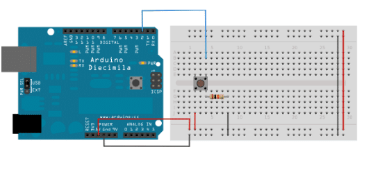 The operation may be done with the following steps:
Take 3 pieces of jumper wires and hook them up with your Arduino board.Two of the wires, red and black, goes to the two long vertical rows on the side of the breadboard which become the supply cords of the board in order to carry the required 5V DC to the board.
The third wire is used for connecting the digital pin 2 to one of the leads of the push-to-ON switch.
This particular lead of the button also links up with a pull-down 10k resistorto the negative supply rail or the ground.The other free lead of the switch is linked with the positive of 5 volt supply.
With the above connections made, the switch toggles or performs a dual action in the circuit when given a push.
Normally when the switch is in a disconnected position, its two leads stay isolated, such that the pin which is linked with the ground via the pull-down resistor renders a LOW, or a logic 0 level.
In the pressed situation the switch executes a momentary a bridging of its two leads, such that its leads are subjected to +5 volts, rendering a HIGH, or logic 1 level across them.
Isolating the digital i/o pinouts from rest of the things, could force the LED to go haywire and cause erratic blinking.
This is due to the fact the input being not rendered to anything, or kept in a "hanging" position - meaning it's not designated to any definite logic, neither high nor low ( +5V or 0V), this is reason why we employ the pull-down resistor with the switch.
The operation may be done with the following steps:
Take 3 pieces of jumper wires and hook them up with your Arduino board.Two of the wires, red and black, goes to the two long vertical rows on the side of the breadboard which become the supply cords of the board in order to carry the required 5V DC to the board.
The third wire is used for connecting the digital pin 2 to one of the leads of the push-to-ON switch.
This particular lead of the button also links up with a pull-down 10k resistorto the negative supply rail or the ground.The other free lead of the switch is linked with the positive of 5 volt supply.
With the above connections made, the switch toggles or performs a dual action in the circuit when given a push.
Normally when the switch is in a disconnected position, its two leads stay isolated, such that the pin which is linked with the ground via the pull-down resistor renders a LOW, or a logic 0 level.
In the pressed situation the switch executes a momentary a bridging of its two leads, such that its leads are subjected to +5 volts, rendering a HIGH, or logic 1 level across them.
Isolating the digital i/o pinouts from rest of the things, could force the LED to go haywire and cause erratic blinking.
This is due to the fact the input being not rendered to anything, or kept in a "hanging" position - meaning it's not designated to any definite logic, neither high nor low ( +5V or 0V), this is reason why we employ the pull-down resistor with the switch.
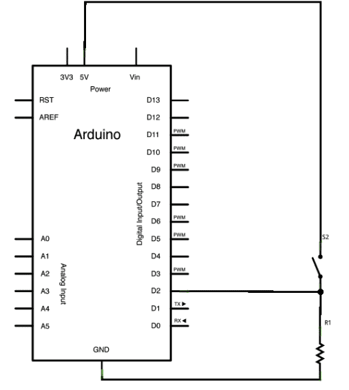

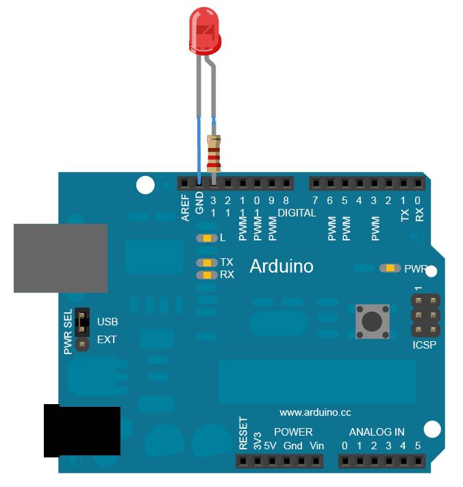
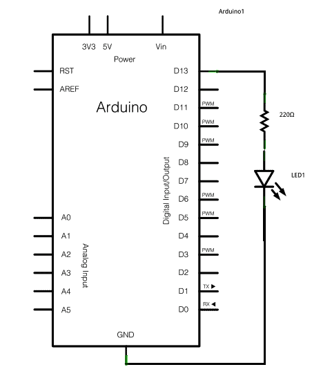
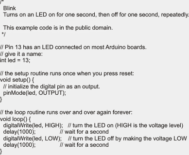

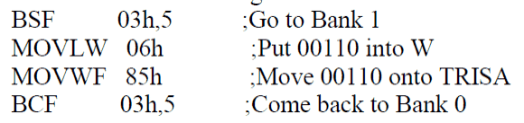
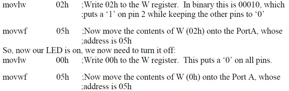
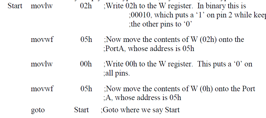
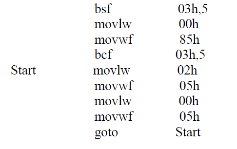
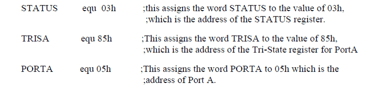
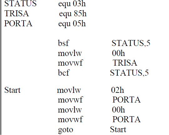

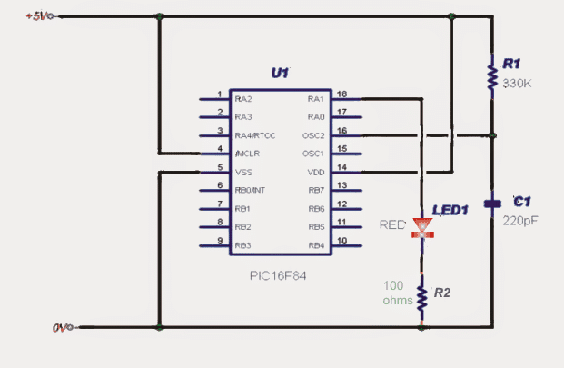
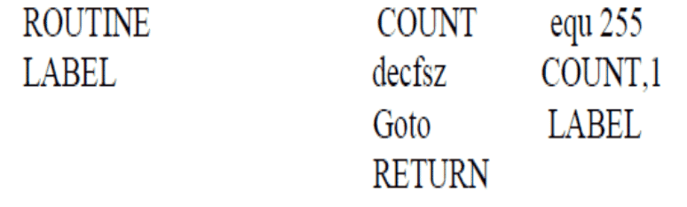
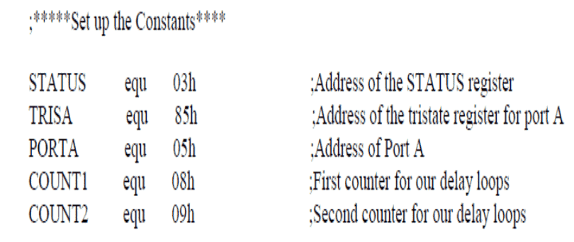
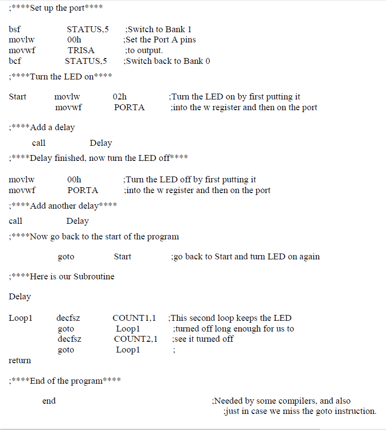
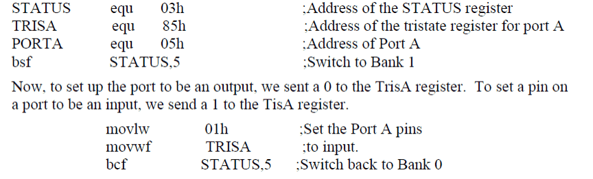
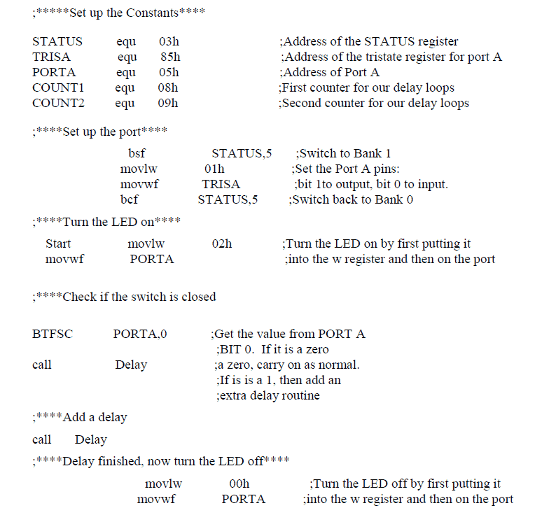
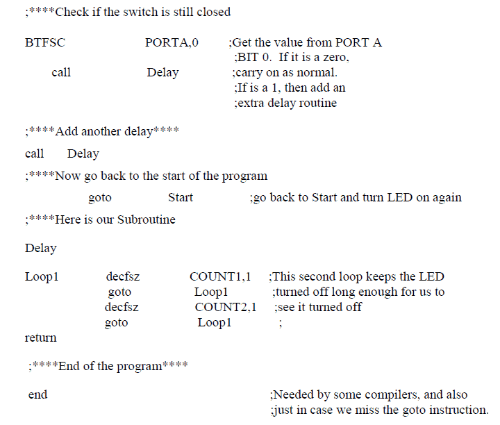
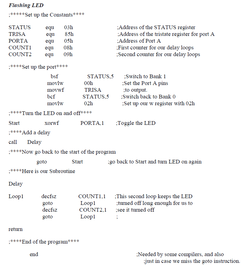
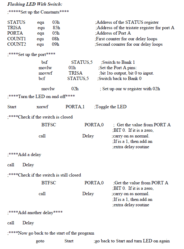
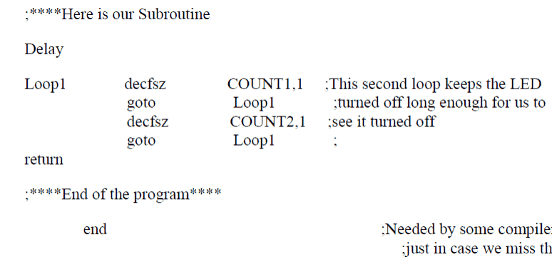
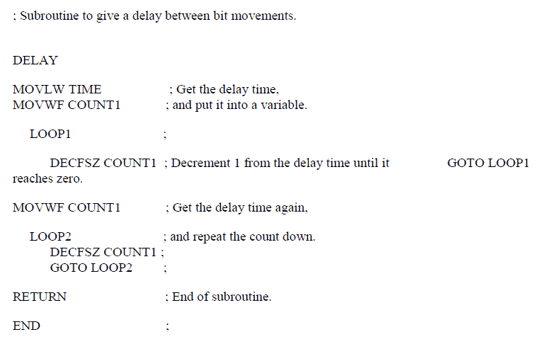
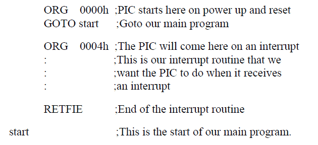
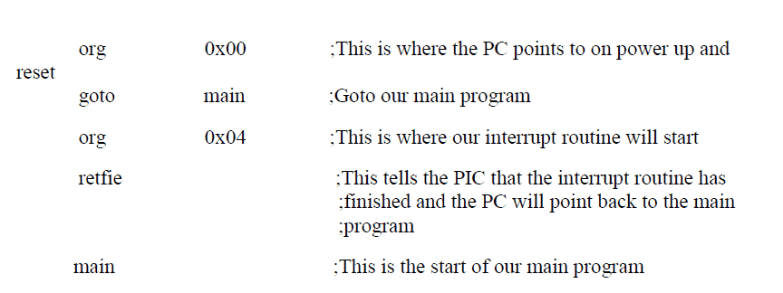
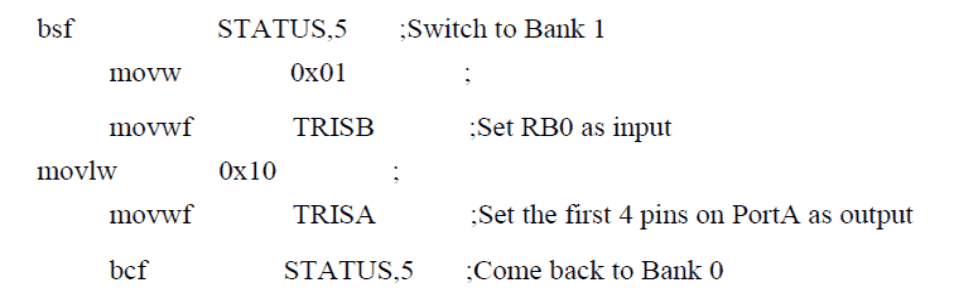
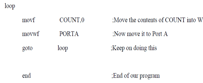
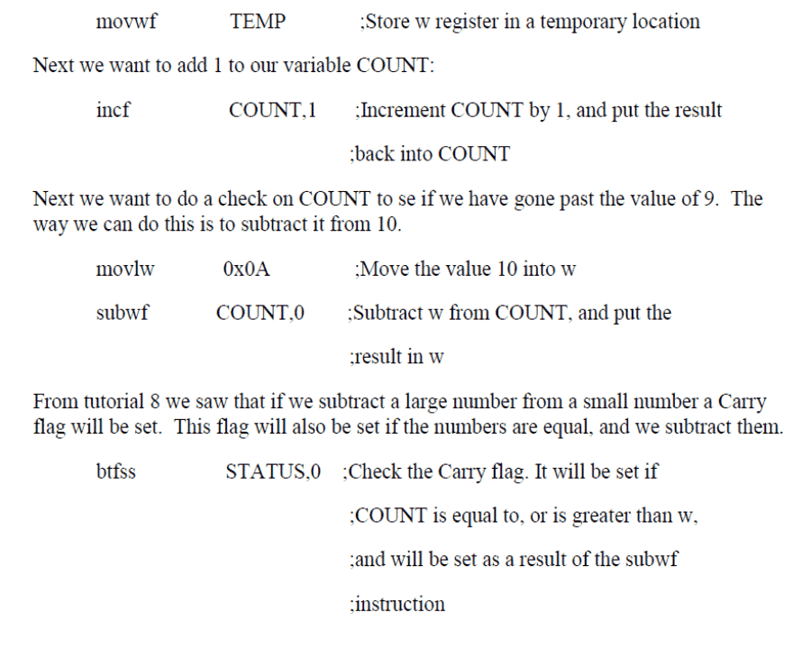
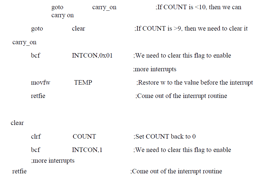
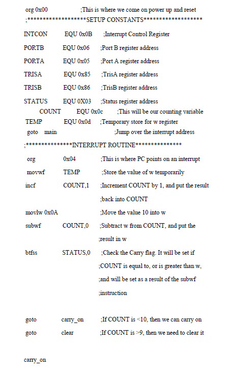

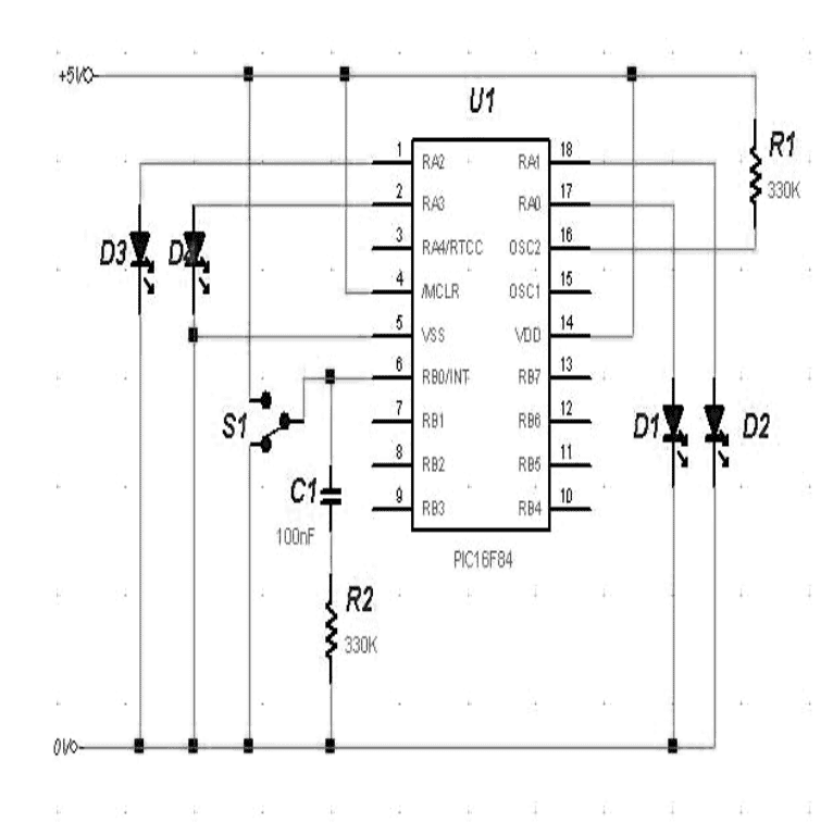
 Consequently, this low-pass filter accepts low-frequency signals while rejecting (significantly attenuating) high-frequency signals.
At a cutoff frequency (fc), the output of this filter rolls-off by 3 decibels (dB), where:
(1) fc = 1 /(2¦ĐRC)
As demonstrated in Fig.
1-b, as frequency increases exceeding the cutoff, frequency rolls-off at a rate of 6 dB/octave (20 dB/decade).
As a result, a 1 kHz low-pass filter cuts a 4 kHz input signal by 12 dB and a 10 kHz signal by 20 dB.
Figure 2-a depicts a second fundamental, passive RC filter,which is an L-section capacitor-input filter.
At lower frequency, the capacitor also functions like an open circuit, whereas at high frequencies, it acts like a short circuit.
As a result, this high pass filter allows high-frequency signals to travel through while rejecting low-frequency ones.
Consequently, this low-pass filter accepts low-frequency signals while rejecting (significantly attenuating) high-frequency signals.
At a cutoff frequency (fc), the output of this filter rolls-off by 3 decibels (dB), where:
(1) fc = 1 /(2¦ĐRC)
As demonstrated in Fig.
1-b, as frequency increases exceeding the cutoff, frequency rolls-off at a rate of 6 dB/octave (20 dB/decade).
As a result, a 1 kHz low-pass filter cuts a 4 kHz input signal by 12 dB and a 10 kHz signal by 20 dB.
Figure 2-a depicts a second fundamental, passive RC filter,which is an L-section capacitor-input filter.
At lower frequency, the capacitor also functions like an open circuit, whereas at high frequencies, it acts like a short circuit.
As a result, this high pass filter allows high-frequency signals to travel through while rejecting low-frequency ones.
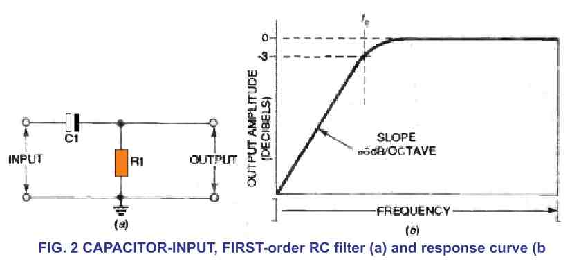 As calculated by the aboveformula (1) implemented to the low-pass filter in Fig.
1-a, the output of this high-pass filter is 3 dB lower at thecutoff frequency.
As the frequency is lowered below this threshold, it rolls off at a 6 dB/octave rate, as illustrated in Fig.
2-b.
As a result, a 1 kHz high-pass filter suppresses the signal by 12 dB to 100 Hz.
As calculated by the aboveformula (1) implemented to the low-pass filter in Fig.
1-a, the output of this high-pass filter is 3 dB lower at thecutoff frequency.
As the frequency is lowered below this threshold, it rolls off at a 6 dB/octave rate, as illustrated in Fig.
2-b.
As a result, a 1 kHz high-pass filter suppresses the signal by 12 dB to 100 Hz.
 This is a second-order, unity-gain low-pass filter havinga cutoff frequency of 10 kHz.
In the passband, the Butterworth filter has a significantlyflat amplitude response, along witha modestsettling time, and amodest overshoot.
Above 10 kHz, the output of this circuit rolls off by12 dB every octave.
At 100 kHz, for instance, the output might be 40 dB lower.
The Butterworth filter's cutoff frequency can becalculated using the following formula:
(2) fc = 1 /(2.83¦ĐRC)
You can change the settings of the resistors and capacitors in the active filter to change the cutoff frequency.
If the value of the resistor or capacitor is known, the variables in formulae (1) or (2) (as applicable) could be adjusted to work outa given cutoff frequency.
The need that one of the capacitor values in the Fig.
3 design be exactly double the value of the other appears to bea small drawback.
(Capacitor C2 in Fig.
3 has a value that's two timesthe value of C1).
This restriction usually necessitates the use of nonstandard capacitor values.
Figure 4 depicts a different active low-pass filter.
It's a second-order filter featuringa cutoff frequency of 10 kHz that addresses the problem with the circuit in Fig.
3.
This is a second-order, unity-gain low-pass filter havinga cutoff frequency of 10 kHz.
In the passband, the Butterworth filter has a significantlyflat amplitude response, along witha modestsettling time, and amodest overshoot.
Above 10 kHz, the output of this circuit rolls off by12 dB every octave.
At 100 kHz, for instance, the output might be 40 dB lower.
The Butterworth filter's cutoff frequency can becalculated using the following formula:
(2) fc = 1 /(2.83¦ĐRC)
You can change the settings of the resistors and capacitors in the active filter to change the cutoff frequency.
If the value of the resistor or capacitor is known, the variables in formulae (1) or (2) (as applicable) could be adjusted to work outa given cutoff frequency.
The need that one of the capacitor values in the Fig.
3 design be exactly double the value of the other appears to bea small drawback.
(Capacitor C2 in Fig.
3 has a value that's two timesthe value of C1).
This restriction usually necessitates the use of nonstandard capacitor values.
Figure 4 depicts a different active low-pass filter.
It's a second-order filter featuringa cutoff frequency of 10 kHz that addresses the problem with the circuit in Fig.
3.
 The values of the capacitors R4 and R5 are the same.
In both theFigs., the ordinary IC741 op-amp is used, which uses the resistors R1 and R2, 3 and 4 tooffer a voltage gain of 4.1 dB.
These must match the figures usedin Fig.
4. Formula (1) may be used to get the cutoff frequency for this "equal components." filter.
Figure 5 illustrates the method of cascadingthese "equal component" filters to create a fourth-order low-pass filter havinga 24 dB/octave rolloff.
The values of the capacitors R4 and R5 are the same.
In both theFigs., the ordinary IC741 op-amp is used, which uses the resistors R1 and R2, 3 and 4 tooffer a voltage gain of 4.1 dB.
These must match the figures usedin Fig.
4. Formula (1) may be used to get the cutoff frequency for this "equal components." filter.
Figure 5 illustrates the method of cascadingthese "equal component" filters to create a fourth-order low-pass filter havinga 24 dB/octave rolloff.
 The resistive divider of R1/R2 which determines the gainin this circuitis 39 kilohms divided by 5.87 kilohms, or 6.644. The R3/R4 potential divideris built using39 kilohms/48.5 kilohms, resulting a value of0.805. This providesa total voltage gain of 8.3 dB for the circuit.
To get the nonstandard R2 and R4 values, you can hook upa couple of standard 5 percent tolerance resistors in series to match the values indicated.
A second-order, 100-Hz, high-pass filter with unity gain is shown in Figure 6.
The resistive divider of R1/R2 which determines the gainin this circuitis 39 kilohms divided by 5.87 kilohms, or 6.644. The R3/R4 potential divideris built using39 kilohms/48.5 kilohms, resulting a value of0.805. This providesa total voltage gain of 8.3 dB for the circuit.
To get the nonstandard R2 and R4 values, you can hook upa couple of standard 5 percent tolerance resistors in series to match the values indicated.
A second-order, 100-Hz, high-pass filter with unity gain is shown in Figure 6.
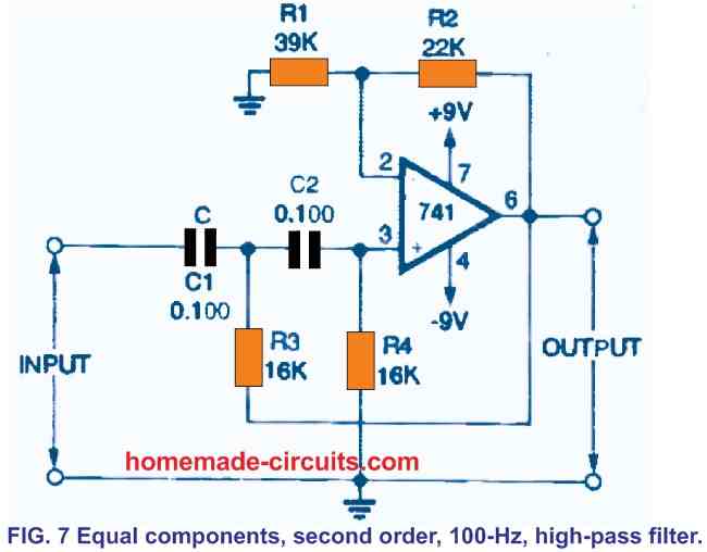 R2 is a resistor with double the resistance of R1.
Figure 7 shows a "equal component" variant of the filter, wherein R3 and R4 are the same.
A fourth-order high-pass filter is shown in Figure 8. The working frequencies of the filters in Figs.
6 and 7 as well as those in
R2 is a resistor with double the resistance of R1.
Figure 7 shows a "equal component" variant of the filter, wherein R3 and R4 are the same.
A fourth-order high-pass filter is shown in Figure 8. The working frequencies of the filters in Figs.
6 and 7 as well as those in
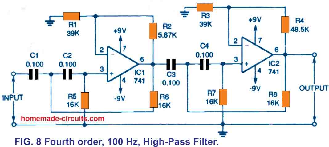 Figs.
4 and 5 may be changed in the same manner asthe working frequencies of the Fig.
2 concept could be changed.
You may increase the values of theresistor and capacitor in orderto decrease the cutoff frequency, or vice versa.
Figure 9 illustrates the method through which thehigh-pass filter circuit from Figure 7 and the low-pass filter schematic from Figure 4 could be combined in series to generate a 300-Hz to 3.4-kHz speech band-pass filter (with appropriate partvalue adjustments).
Figs.
4 and 5 may be changed in the same manner asthe working frequencies of the Fig.
2 concept could be changed.
You may increase the values of theresistor and capacitor in orderto decrease the cutoff frequency, or vice versa.
Figure 9 illustrates the method through which thehigh-pass filter circuit from Figure 7 and the low-pass filter schematic from Figure 4 could be combined in series to generate a 300-Hz to 3.4-kHz speech band-pass filter (with appropriate partvalue adjustments).
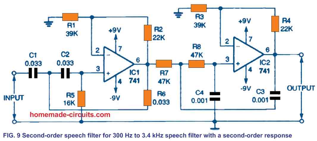 All frequencies that areoutside thisfrequency range are rejected by 12dB/octave.
To boost the cutoff frequency from 100 Hz to 300 Hz in the high-pass filter shown in Figure 7, the capacitor values are 1/3rdof the original numbers.
We multiply the original resistor values with2.94 in the low-pass filter of Fig.
4 to decrease the cutoff frequency from 10kHz to 3.4 kHz.
All frequencies that areoutside thisfrequency range are rejected by 12dB/octave.
To boost the cutoff frequency from 100 Hz to 300 Hz in the high-pass filter shown in Figure 7, the capacitor values are 1/3rdof the original numbers.
We multiply the original resistor values with2.94 in the low-pass filter of Fig.
4 to decrease the cutoff frequency from 10kHz to 3.4 kHz.
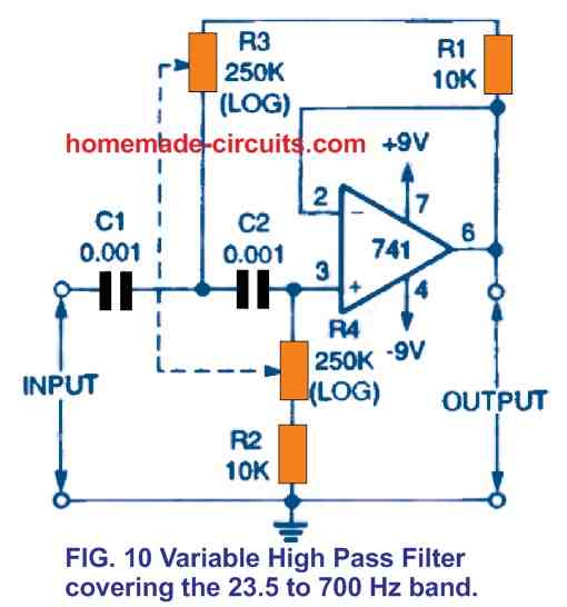 (These could be ganged mechanically.) Because the resistors in the RC networks in this circuit contain equal values (unlike those in Fig.
6), this configuration doesn't really produce one of most flat Butterworth filter characteristic.
Nonetheless, it provides excellent signal quality .
This filter's "static" version typically has a cutoff frequency of 50 Hz.
The Fig.
11 circuit designis a modifiedversion of the Fig.
3 high-pass filter, although its cutoff frequency is entirely adjustable from 2.2 kHz to 24 kHz through constant adjustment of paired potentiometers R3 and R4. (These, too, could be ganged.) This filter, like the one in Fig.
10, doesn't really exhibit the most flat Butterworth feature.
(These could be ganged mechanically.) Because the resistors in the RC networks in this circuit contain equal values (unlike those in Fig.
6), this configuration doesn't really produce one of most flat Butterworth filter characteristic.
Nonetheless, it provides excellent signal quality .
This filter's "static" version typically has a cutoff frequency of 50 Hz.
The Fig.
11 circuit designis a modifiedversion of the Fig.
3 high-pass filter, although its cutoff frequency is entirely adjustable from 2.2 kHz to 24 kHz through constant adjustment of paired potentiometers R3 and R4. (These, too, could be ganged.) This filter, like the one in Fig.
10, doesn't really exhibit the most flat Butterworth feature.
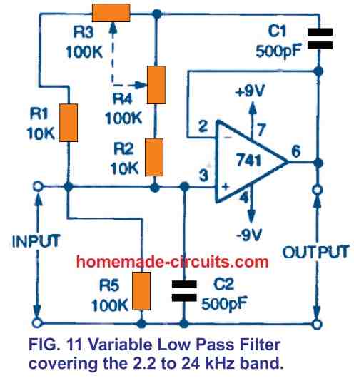 This designis actuallyanexcellentscratch noise removal filter.
The cutoff frequency of "fixed" versions of this filter is generally 10 kHz.
Figure 12 depicts the method in which thefilters in Figures 10 and 11 could be coupled to produce a flexible, adjustable high-pass/low-pass filter for eliminating rumble and scratch noise from voiceaudio.
This designis actuallyanexcellentscratch noise removal filter.
The cutoff frequency of "fixed" versions of this filter is generally 10 kHz.
Figure 12 depicts the method in which thefilters in Figures 10 and 11 could be coupled to produce a flexible, adjustable high-pass/low-pass filter for eliminating rumble and scratch noise from voiceaudio.
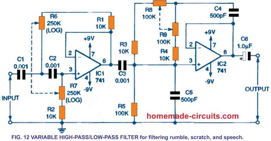 The low-pass and high-pass cutoff frequencies are both completelyadjustable.
The high-pass cutoff frequency could be adjusted from 23.5 Hz to 700 Hz by evenly altering thematched (or ganged) potentiometers R6 and R7. R8 and R9 may also change the low-pass frequency between 2.2 kHz and 24 kHz.
The low-pass and high-pass cutoff frequencies are both completelyadjustable.
The high-pass cutoff frequency could be adjusted from 23.5 Hz to 700 Hz by evenly altering thematched (or ganged) potentiometers R6 and R7. R8 and R9 may also change the low-pass frequency between 2.2 kHz and 24 kHz.
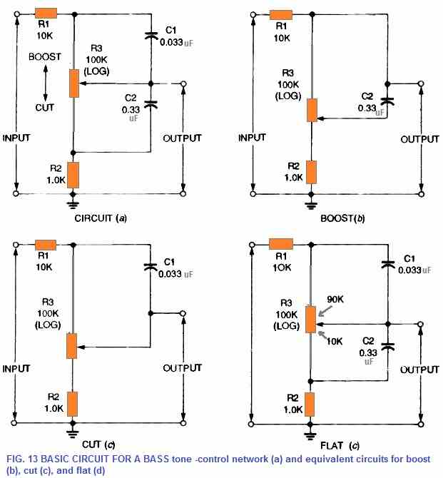 The direction of pot slider rotationto get boost (up) and cut is indicated by the vertical double-ended arrow adjacent to trimmer potentiometer R3 (down).
The corresponding circuits are shown in Figures 13-b to 13-d when potentiometer R3 is adjusted to highest boost, highest cut, and flat, respectively.
Once the frequency is setat its minimum bass value, capacitors C1 and C2 are fully open-circuited.
As a result, the boost circuit becomes proportional to a 10 kilohm resistor divided by a 101 kilohm resistor, as can be seen in Fig.
13-b.
Only a little amount of bass is attenuated.
By comparison, the Fig.
13 -c cut equivalent circuit is equivalent to a 110 kilohm resistor divided by a 1.0 kilohm resistor.
Bass signals are attenuated by roughly 40 decibels as a result of this.
Figure 13-d illustrates the flat setting of potentiometer R3.
In this set up the resistive element can be seen as90 kilohms above the slider of the potand 10 kilohms below it.
A 100-kilohm resistor is divided by an 11-kilohm resistor to create the aboveconfiguration.
Throughout all frequencies, this circuit generates roughly 20 dB of attenuation.
Due to this, the circuit is able toprovidea maximum bass boost or reductionof around 20 dB when compared to flat frequencies.
A typical design for a passive treble tone-control configurationis shown in Figure 14-a.
Inside the 20 to 20,000 kHz frequency range, the system is able toefficiently amplify or decrease high-audio frequencies.
Technically identical circuits are shown in Figures 14-b to 13d during optimum boost, optimumreduction, and duringflat operating conditions, respectively.
The direction of pot slider rotationto get boost (up) and cut is indicated by the vertical double-ended arrow adjacent to trimmer potentiometer R3 (down).
The corresponding circuits are shown in Figures 13-b to 13-d when potentiometer R3 is adjusted to highest boost, highest cut, and flat, respectively.
Once the frequency is setat its minimum bass value, capacitors C1 and C2 are fully open-circuited.
As a result, the boost circuit becomes proportional to a 10 kilohm resistor divided by a 101 kilohm resistor, as can be seen in Fig.
13-b.
Only a little amount of bass is attenuated.
By comparison, the Fig.
13 -c cut equivalent circuit is equivalent to a 110 kilohm resistor divided by a 1.0 kilohm resistor.
Bass signals are attenuated by roughly 40 decibels as a result of this.
Figure 13-d illustrates the flat setting of potentiometer R3.
In this set up the resistive element can be seen as90 kilohms above the slider of the potand 10 kilohms below it.
A 100-kilohm resistor is divided by an 11-kilohm resistor to create the aboveconfiguration.
Throughout all frequencies, this circuit generates roughly 20 dB of attenuation.
Due to this, the circuit is able toprovidea maximum bass boost or reductionof around 20 dB when compared to flat frequencies.
A typical design for a passive treble tone-control configurationis shown in Figure 14-a.
Inside the 20 to 20,000 kHz frequency range, the system is able toefficiently amplify or decrease high-audio frequencies.
Technically identical circuits are shown in Figures 14-b to 13d during optimum boost, optimumreduction, and duringflat operating conditions, respectively.
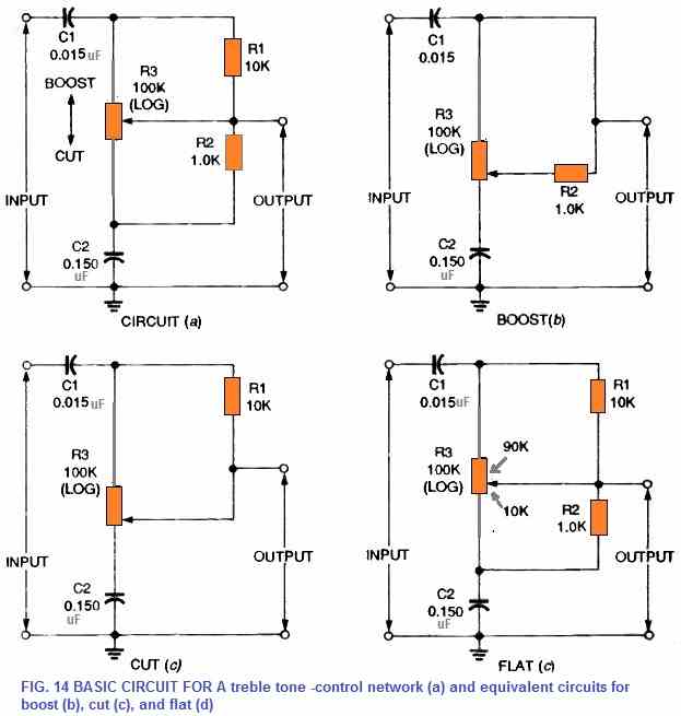 When R3 is moved aroundthe flat position, this circuit provides around 20 dB of signal attenuation and highest possibletreble, boost, or reduction values of 20 dB compared to the circuits'flat regionperformance.
Figure 15 illustrates the method through which thecircuits in Figures 13 a and 14 a may be interconnected to provide a comprehensive passive bass and treble tone-control configuration.
When R3 is moved aroundthe flat position, this circuit provides around 20 dB of signal attenuation and highest possibletreble, boost, or reduction values of 20 dB compared to the circuits'flat regionperformance.
Figure 15 illustrates the method through which thecircuits in Figures 13 a and 14 a may be interconnected to provide a comprehensive passive bass and treble tone-control configuration.
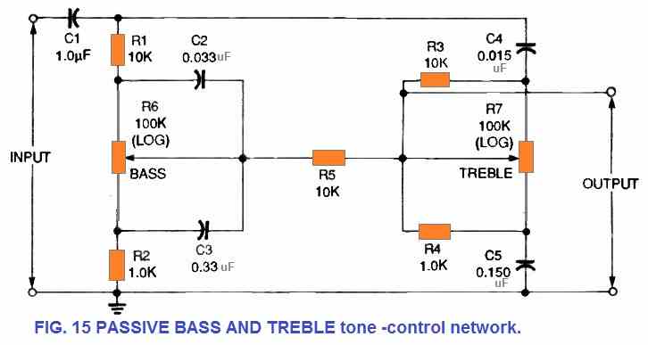 To avoid undesired interactions between the different portions of the circuit, a 10 kilohm resistor R5 has been introduced in the network.
The output of this circuit may be fed to the input of a primary power amplifier, whilethe input could be obtaineddirectly from an amplifier's volume control.
To avoid undesired interactions between the different portions of the circuit, a 10 kilohm resistor R5 has been introduced in the network.
The output of this circuit may be fed to the input of a primary power amplifier, whilethe input could be obtaineddirectly from an amplifier's volume control.
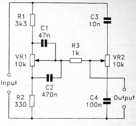 Due to the passive characteristics of the circuit, it isn't actually appropriate to assess in terms of the controls delivering boost and cut.
Such designs will always present losses, and if configured to offer bass or treble boost it is in reality delivering diminished losses instead of a authentic boost to the signal level.
This may not be strictly academic, and the technique in general has to be built to consider the fundamental loss of around 12dB associated with such designs.
Due to the passive characteristics of the circuit, it isn't actually appropriate to assess in terms of the controls delivering boost and cut.
Such designs will always present losses, and if configured to offer bass or treble boost it is in reality delivering diminished losses instead of a authentic boost to the signal level.
This may not be strictly academic, and the technique in general has to be built to consider the fundamental loss of around 12dB associated with such designs.
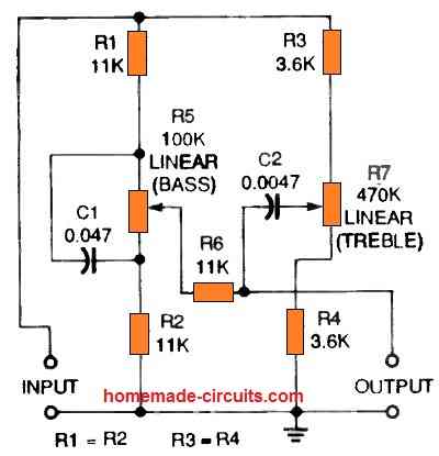 This happens since capacitor C2 isolates resistor R6 from the output.
The amplitudes of theoutput signal are entirely controlled by resistor R6 at input frequencies large enough to cause the two capacitors to behave as short circuits.
Resistor R5 is short-circuited through C1 in this case.
The values of R1and C1decidethe low-frequency (bass) circuit cutoff, whereas C2 and the quantities of R1to R3 define the high-frequency (treble) circuit cutoff.
The next figure below revealshow the design in the above figurecan beincorporated into an active tone control circuit which may amplify or reduce bass or treble signals by up to 20 decibels (dB).
This happens since capacitor C2 isolates resistor R6 from the output.
The amplitudes of theoutput signal are entirely controlled by resistor R6 at input frequencies large enough to cause the two capacitors to behave as short circuits.
Resistor R5 is short-circuited through C1 in this case.
The values of R1and C1decidethe low-frequency (bass) circuit cutoff, whereas C2 and the quantities of R1to R3 define the high-frequency (treble) circuit cutoff.
The next figure below revealshow the design in the above figurecan beincorporated into an active tone control circuit which may amplify or reduce bass or treble signals by up to 20 decibels (dB).
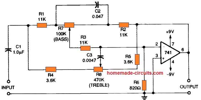 Although comparable to the above this active tone control circuit indicated in the nextin figure looksevenmore flexible.
It contains an extra filter control circuitrythat is centered withinthe audio spectrum's 1 kHz midband.
The midband may be enhanced or reduced by up to 20 dB using this network.
Although comparable to the above this active tone control circuit indicated in the nextin figure looksevenmore flexible.
It contains an extra filter control circuitrythat is centered withinthe audio spectrum's 1 kHz midband.
The midband may be enhanced or reduced by up to 20 dB using this network.
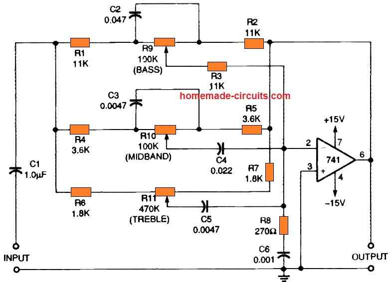 It is generally advised that instead of messing with passive circuits, it is better to go for an active tone control circuit like the one demonstrated in the following circuit diagram.
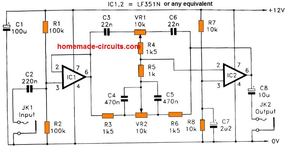 This is simply a passive tone control hooked up from the feedback circuit of a non-inverting op amp amplifier, along with an input buffer stage to ensure that the primary tone control circuit is operated through a appropriately low source impedance.
This offers a kind of inverted results, in which boost from the tone controls supplies increased feedback and decreased gain, while the cut from the controls offers reduced feedback and increased gain.
If the two potentiometers are connected considering these factors, it might be able to deliver the right results through the controls (meaning clockwise movement of the pot will produce boost; and anti-clockwise rotation will deliver cut).
The indicated tone control circuit supplies slightly above 12dB of boost and cut within the opposite limits of the music range.
This is simply a passive tone control hooked up from the feedback circuit of a non-inverting op amp amplifier, along with an input buffer stage to ensure that the primary tone control circuit is operated through a appropriately low source impedance.
This offers a kind of inverted results, in which boost from the tone controls supplies increased feedback and decreased gain, while the cut from the controls offers reduced feedback and increased gain.
If the two potentiometers are connected considering these factors, it might be able to deliver the right results through the controls (meaning clockwise movement of the pot will produce boost; and anti-clockwise rotation will deliver cut).
The indicated tone control circuit supplies slightly above 12dB of boost and cut within the opposite limits of the music range.
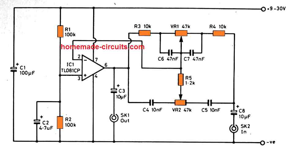 When the wiper arm of VR1 and VR2 are turned fully towards left side, it results in maximum feedback, producing full bass and treble cut.
When the wipers are moved at the opposite side of their rotation we get lowest feedback and thus highest bass and treble boost.
The controls don't have any substantial impact at central audio frequencies (around 800Hz), and offer highest boost and attenuation value of approximately 12dB.
The total level of cut and boost is actually offered at the two extremes of the music frequency range, and 12dB is around the maximum that will actually be required in real life use.
1C1 is wired in the inverting mode, and its non-inverting input is as a result easily biased to 50 % of the supply voltage through R1 and R2. C2 is used for decoupling any noise that might normally be supplied to the non-inverting input through the supply rails through R1 and R2, or picked-up because of to stray coupling.
The amounts of noise and distortion generated by the circuit are minimal, even while the pot controls are adjusted for getting highest possible boost (which still allows the the circuit to have just an extremely minimal level of voltage gain).
As soon as one or both of the tone controls are adjusted for a cut, IC1 offers a closed loop gain of lower than unity.
Using certain inside compensated operational amplifiers a closed loop gain of smaller than unity may trigger instability, and the internal compensation is simply for closed loop voltage gains of unity or higher.
A number of TL081 CP ICs had been experimented with in the circuit and zero complications with instability were encountered.
The circuit may additionally perform nicely using a 741C IC, and in real life use is unlikely that any kind of recognizable drop in efficiency would actually be noticeable employing IC 741. However, the noise and distortion quantities will probably be somewhat greater compared to the IC TL081CP.
When the wiper arm of VR1 and VR2 are turned fully towards left side, it results in maximum feedback, producing full bass and treble cut.
When the wipers are moved at the opposite side of their rotation we get lowest feedback and thus highest bass and treble boost.
The controls don't have any substantial impact at central audio frequencies (around 800Hz), and offer highest boost and attenuation value of approximately 12dB.
The total level of cut and boost is actually offered at the two extremes of the music frequency range, and 12dB is around the maximum that will actually be required in real life use.
1C1 is wired in the inverting mode, and its non-inverting input is as a result easily biased to 50 % of the supply voltage through R1 and R2. C2 is used for decoupling any noise that might normally be supplied to the non-inverting input through the supply rails through R1 and R2, or picked-up because of to stray coupling.
The amounts of noise and distortion generated by the circuit are minimal, even while the pot controls are adjusted for getting highest possible boost (which still allows the the circuit to have just an extremely minimal level of voltage gain).
As soon as one or both of the tone controls are adjusted for a cut, IC1 offers a closed loop gain of lower than unity.
Using certain inside compensated operational amplifiers a closed loop gain of smaller than unity may trigger instability, and the internal compensation is simply for closed loop voltage gains of unity or higher.
A number of TL081 CP ICs had been experimented with in the circuit and zero complications with instability were encountered.
The circuit may additionally perform nicely using a 741C IC, and in real life use is unlikely that any kind of recognizable drop in efficiency would actually be noticeable employing IC 741. However, the noise and distortion quantities will probably be somewhat greater compared to the IC TL081CP.
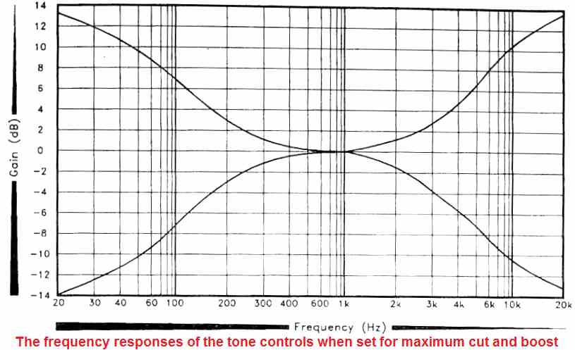 Having said that, remember the potentiometer tolerance can be pretty extensive at around 20%, and that the physical center point of adjustment can be impossible to be the correct electrical center-point.
Any kind of errors caused by this situation within the theoretically flat frequency response could be rather insignificant though.
Building of the tone controls provides hardly any issues.
The voltage gain is so minimal, that even if the control is adjusted for getting optimum boost, there could be absolutely no risk of instability.
Having said that, remember the potentiometer tolerance can be pretty extensive at around 20%, and that the physical center point of adjustment can be impossible to be the correct electrical center-point.
Any kind of errors caused by this situation within the theoretically flat frequency response could be rather insignificant though.
Building of the tone controls provides hardly any issues.
The voltage gain is so minimal, that even if the control is adjusted for getting optimum boost, there could be absolutely no risk of instability.
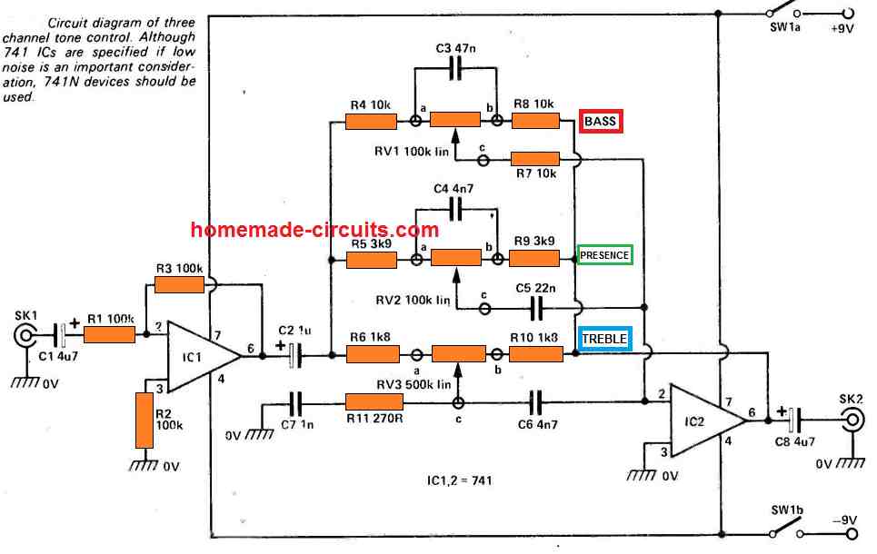 The first op amp stage needs to be kept isolated from the next stage due to prevent loading effects.
The ICI output is applied through 3 frequency shaping circuit configurations to IC2. The three tone controls are constructed around the pots RV1, RV2, RV3 which additionally form the part of the feedback path of IC2, which is configured like another inverting op amp stage.
The parts used around the three potentiometer are selected such that it delivers the intended frequency and tone control results.
The first op amp stage needs to be kept isolated from the next stage due to prevent loading effects.
The ICI output is applied through 3 frequency shaping circuit configurations to IC2. The three tone controls are constructed around the pots RV1, RV2, RV3 which additionally form the part of the feedback path of IC2, which is configured like another inverting op amp stage.
The parts used around the three potentiometer are selected such that it delivers the intended frequency and tone control results.
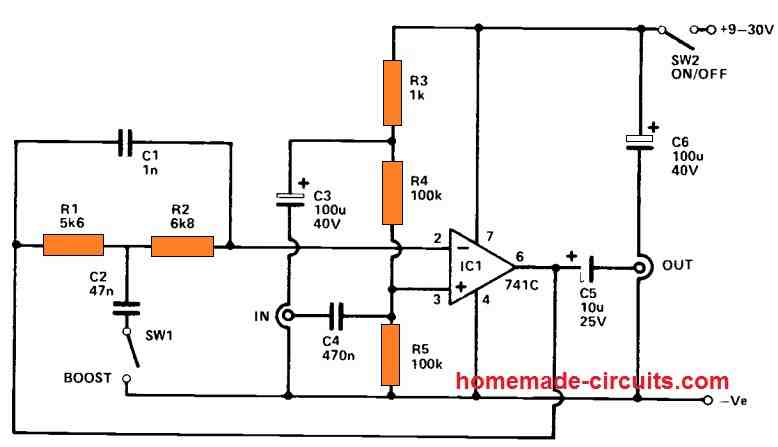 In order to provide high stability and a reducednoise level, it is common to place just a little amount of importance on the upper-treble.
This also avoids the output from appearing excessively harsh.
The frequency response is seen in the graph below.
In order to provide high stability and a reducednoise level, it is common to place just a little amount of importance on the upper-treble.
This also avoids the output from appearing excessively harsh.
The frequency response is seen in the graph below.
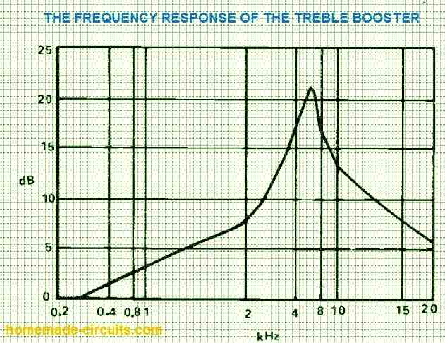 The design is essentially an op amp operating in non-inverting mode.
R4 and R5 bias the non-inverting input through a decoupling network consisting of R3 and C3. DC blocking is provided by C4 and C5 at the input and output, accordingly.
With SW1 inopen condition, R1, R2, and C1 provide nearly 100 percent negative feedback, providing the circuit unit gain and a flat response.
By closing SW1, part of the feedback via R1 and R2 is decoupled at frequencies greater than just few 100 Hz, resulting in the desired ascending response.
At peaktreble frequencies, feedback through C1 enables the response to fade away over around 5.5 kHz, preventing the extremely high frequency harmonics from gettingover emphasized.
The design is essentially an op amp operating in non-inverting mode.
R4 and R5 bias the non-inverting input through a decoupling network consisting of R3 and C3. DC blocking is provided by C4 and C5 at the input and output, accordingly.
With SW1 inopen condition, R1, R2, and C1 provide nearly 100 percent negative feedback, providing the circuit unit gain and a flat response.
By closing SW1, part of the feedback via R1 and R2 is decoupled at frequencies greater than just few 100 Hz, resulting in the desired ascending response.
At peaktreble frequencies, feedback through C1 enables the response to fade away over around 5.5 kHz, preventing the extremely high frequency harmonics from gettingover emphasized.
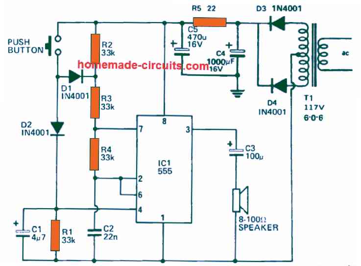 However, because the upper end of the capacitor is linked with both pin#2 and pin#6 of the IC, therefore, as soon as the voltage across the capacitor tends to reach 6V level, the two internal comparators of the IC gets above their threshold level, causing the IC 555 at pin#3 to go low, which in turn results in the internal transistor of the IC to switch on.
The action short circuits the pin#7 of the IC to ground.
But, since pin#7 is hooked up with the junction of the resistors R3 and R4 and C2, now begins getting discharged by means of the resistor R4.
During this process as soon as the voltage stored inside C2 tends to drop below 3 V, causes the output of the IC to yet again go high, switching OFF the internal transistor of the IC.
This in turn immediately causes C2 to start charging again by means of the resistor R2, R3 and R4.
This sequence of action goes on repeating continuously, which causes the generation of triangular waveform across C2, creating a train of pulses at the IC output pin#3.
This train of pulses coming out from the pin#3 of the IC can be seen configured with a loudspeaker by means of the capacitor C3.
The C3 capacitor ensures that the dc component present in the pin#3 output voltage does not reach the loudspeaker and thus prevents the loudspeaker from burning.
The capacitor C2 generates the triangular waveform as it charges through 3 V to 6 V and while discharging from 6V to 3V.
If you desire to change the pitch tone of the two tone door bell circuit, to a different tone you just have to tweak the values of the resistors R2, R3, R4 or simply the change the value of C2 appropriately until the desired tone output is achieved.
However, because the upper end of the capacitor is linked with both pin#2 and pin#6 of the IC, therefore, as soon as the voltage across the capacitor tends to reach 6V level, the two internal comparators of the IC gets above their threshold level, causing the IC 555 at pin#3 to go low, which in turn results in the internal transistor of the IC to switch on.
The action short circuits the pin#7 of the IC to ground.
But, since pin#7 is hooked up with the junction of the resistors R3 and R4 and C2, now begins getting discharged by means of the resistor R4.
During this process as soon as the voltage stored inside C2 tends to drop below 3 V, causes the output of the IC to yet again go high, switching OFF the internal transistor of the IC.
This in turn immediately causes C2 to start charging again by means of the resistor R2, R3 and R4.
This sequence of action goes on repeating continuously, which causes the generation of triangular waveform across C2, creating a train of pulses at the IC output pin#3.
This train of pulses coming out from the pin#3 of the IC can be seen configured with a loudspeaker by means of the capacitor C3.
The C3 capacitor ensures that the dc component present in the pin#3 output voltage does not reach the loudspeaker and thus prevents the loudspeaker from burning.
The capacitor C2 generates the triangular waveform as it charges through 3 V to 6 V and while discharging from 6V to 3V.
If you desire to change the pitch tone of the two tone door bell circuit, to a different tone you just have to tweak the values of the resistors R2, R3, R4 or simply the change the value of C2 appropriately until the desired tone output is achieved.
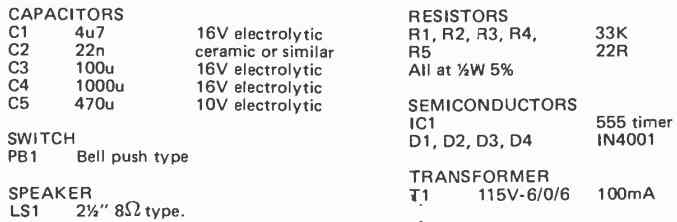
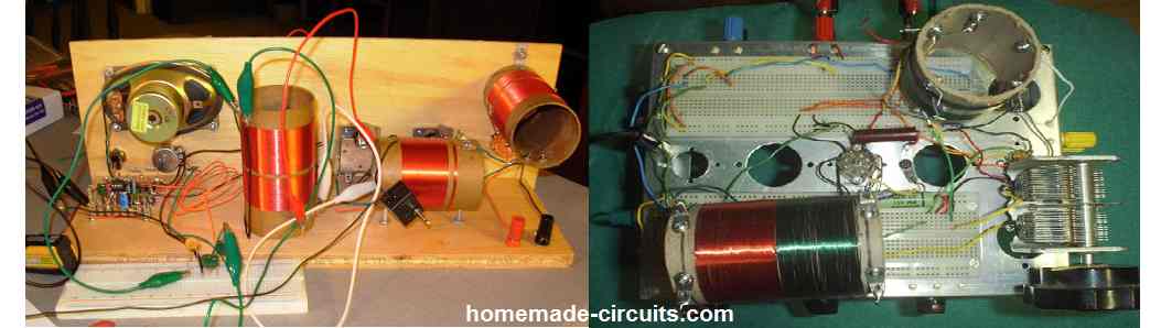 You will find two fundamental types of radio receiver circuits that people can easily construct.
The most straightforward of the two is the receiver that does not require any external power and extracts the RF signals directly from the atmophere and transforms it to sound signal through a single, easy diode rectification step.
This form of well-known passive receiver best remembered as the crystal set or diode radio.
Nearly all basic crystal radios experience difficulty in selectivity and audio output.
In order to strengthen both these attributes, the captured RF level has to be boosted before amplification.
The remedy is to boost the performance of the antenna by putting it to a greater height over the ground and so that it is much longer length wise, or simply to transfer the receiver nearer to the RF signal source.
Typically none of the two solution is looks very practical.
However when we choose to proceed the active way by creating a receiver almost anything that you can do to the signal transmission electronically turns into a fair game.
The RF could be amplified prior to detection step, or changed into a new frequency (IF) to be amplified again prior to detection.
In reality a number of well-known communication radio receivers switch the RF 3 times prior to the modulation data is transformed into sound frequency and directed further for audio frequency (AF), amplification.
All the three of the discussed tuned radio frequency receiver circuits can be classified ideally to be in the active class.
You will find two fundamental types of radio receiver circuits that people can easily construct.
The most straightforward of the two is the receiver that does not require any external power and extracts the RF signals directly from the atmophere and transforms it to sound signal through a single, easy diode rectification step.
This form of well-known passive receiver best remembered as the crystal set or diode radio.
Nearly all basic crystal radios experience difficulty in selectivity and audio output.
In order to strengthen both these attributes, the captured RF level has to be boosted before amplification.
The remedy is to boost the performance of the antenna by putting it to a greater height over the ground and so that it is much longer length wise, or simply to transfer the receiver nearer to the RF signal source.
Typically none of the two solution is looks very practical.
However when we choose to proceed the active way by creating a receiver almost anything that you can do to the signal transmission electronically turns into a fair game.
The RF could be amplified prior to detection step, or changed into a new frequency (IF) to be amplified again prior to detection.
In reality a number of well-known communication radio receivers switch the RF 3 times prior to the modulation data is transformed into sound frequency and directed further for audio frequency (AF), amplification.
All the three of the discussed tuned radio frequency receiver circuits can be classified ideally to be in the active class.
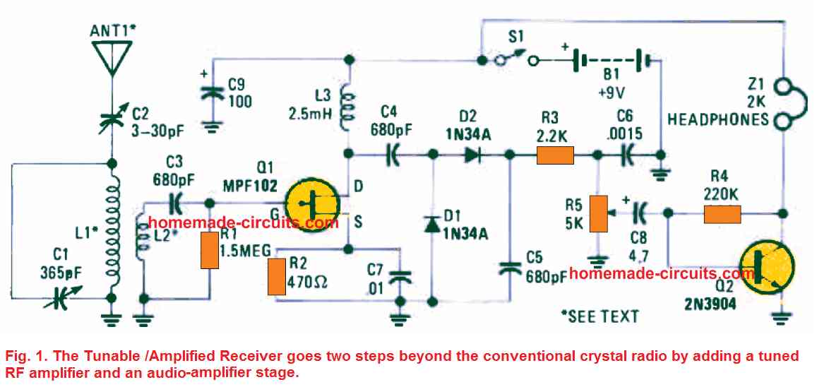 The first discussed TRF receiver circuit (see Fig.
1) moves a couple of steps over and above the standard crystal radio with the addition of a tuned RF amplifier stage before the signal is demodulated and an audio amplifier stage after the demodulation stage.
The RF power through the antenna is applied by using a tiny trimmer capacitor, C2, to the tuned circuit consisting of L1 and C1.
The specified transmitted signal is selected through C1 (a 365 pF GANG capacitor).
Inductor L2 delivers the tuned RF signal towards the RF amplifier input, which includes Q1 which is an MPF102 N-channel, junction field-effect transistor or JFET.
These transistors amplify the RF signal numerous times prior to transferring it onto the detector stage.
A couple of 1N34A germanium diodes (D1 and D2) are hooked up within a voltage doubler/detector circuit which contributes an increased output signal to drive the audio amplifier circuit.
The RF component of the transmission, following detection, is filtered through the components C5, R3, and C6 leaving behind the audio component of the signal towards the input of the volume control, R5. A 2N3904 NPN transistor, configured like a common-emitter circuit, boosts the AF signal to a degree high enough to drive your pair of headphones or, if the signal is powerful from the local stations, a speaker is driven nicely with the help of an impedance-matching transformer.
You could receive a number of stations as soon as an 18-inch clip lead is hooked up to the antenna port.
It may be possible catch six local stations when a 20 -foot length of connecting wire is used clinging through your house ceiling.
The TRF receiver can be nicely operated through just one 9 volt transistor radio PP3 battery.
Because the current usage is just a couple of milliamperes, the battery must go on for many months when the unit is used normally.
Inductors L1 and L2 can be made by winding 20 SWG enamel copper wire over a 2.5 inch long and 4 inch diameter plastic pipe.
The first discussed TRF receiver circuit (see Fig.
1) moves a couple of steps over and above the standard crystal radio with the addition of a tuned RF amplifier stage before the signal is demodulated and an audio amplifier stage after the demodulation stage.
The RF power through the antenna is applied by using a tiny trimmer capacitor, C2, to the tuned circuit consisting of L1 and C1.
The specified transmitted signal is selected through C1 (a 365 pF GANG capacitor).
Inductor L2 delivers the tuned RF signal towards the RF amplifier input, which includes Q1 which is an MPF102 N-channel, junction field-effect transistor or JFET.
These transistors amplify the RF signal numerous times prior to transferring it onto the detector stage.
A couple of 1N34A germanium diodes (D1 and D2) are hooked up within a voltage doubler/detector circuit which contributes an increased output signal to drive the audio amplifier circuit.
The RF component of the transmission, following detection, is filtered through the components C5, R3, and C6 leaving behind the audio component of the signal towards the input of the volume control, R5. A 2N3904 NPN transistor, configured like a common-emitter circuit, boosts the AF signal to a degree high enough to drive your pair of headphones or, if the signal is powerful from the local stations, a speaker is driven nicely with the help of an impedance-matching transformer.
You could receive a number of stations as soon as an 18-inch clip lead is hooked up to the antenna port.
It may be possible catch six local stations when a 20 -foot length of connecting wire is used clinging through your house ceiling.
The TRF receiver can be nicely operated through just one 9 volt transistor radio PP3 battery.
Because the current usage is just a couple of milliamperes, the battery must go on for many months when the unit is used normally.
Inductors L1 and L2 can be made by winding 20 SWG enamel copper wire over a 2.5 inch long and 4 inch diameter plastic pipe.
 Figure 2 shows the way the a pair of inductors should be wound.
Beginning with the 2.5 inch length of plastic pipe, leave around a half inch on the upper section of the coil former and punch a couple of tiny holes through the former in order to tie the start end of L1. Interlace the wire end via the two holes to create a 6-inch pigtail for attaching to C1. Wind the coil tightly, just as we do to wind solenoids, use 25 number of turns to complete L1 inductor.
After this temporarily put an adhesive tape over the the loose end of the winding, make 2 additional small holes on the former, and twine the wire from the holes to clamp the finished coil in position.
Furthermore spare around 6 inches of wire at the L1's finished end in order to enable the connections to C1 and circuit ground.
Leave about an 1/8 inch from L1 end and drill a couple of more holes on the former intended for securing the start end of L2. Keeping a 6 inch pigtail, tightly wind an overall of 8 turns, within the exact same direction as L1.
Punch two more holes on the former and secure by tieing up the ground end of L2 as done in the previous steps, leaving a 6 inch pigtail for connecting to circuit ground.
Because we have just one stage of RF gain, the wiring arrangement isn't very important and any appropriate set up might work.
Regardless of this, make sure to keep all the legs of the components as small as possible and put the 2.5 mH choke (L3) a little distance away from L1 and L2. If you want to use a speaker, you can hook up the primary of any small audio output transformer in place where the phones are connected and attach the speaker to the secondary side of the transformer.
To start using the radio, power it up with a 9 volt battery.
Adjust the tuning of the gang capacitor C1 to different locations, until you finally begin hearing a couple of local stations loud and clear.
Furthermore try connecting a 10 to 20 foot long flexible wire to C2 which will allow you to catch many additional radio stations on your TRF radio set.
Adjust C2 in order to get the finest selectivity among the available radio stations.
Figure 2 shows the way the a pair of inductors should be wound.
Beginning with the 2.5 inch length of plastic pipe, leave around a half inch on the upper section of the coil former and punch a couple of tiny holes through the former in order to tie the start end of L1. Interlace the wire end via the two holes to create a 6-inch pigtail for attaching to C1. Wind the coil tightly, just as we do to wind solenoids, use 25 number of turns to complete L1 inductor.
After this temporarily put an adhesive tape over the the loose end of the winding, make 2 additional small holes on the former, and twine the wire from the holes to clamp the finished coil in position.
Furthermore spare around 6 inches of wire at the L1's finished end in order to enable the connections to C1 and circuit ground.
Leave about an 1/8 inch from L1 end and drill a couple of more holes on the former intended for securing the start end of L2. Keeping a 6 inch pigtail, tightly wind an overall of 8 turns, within the exact same direction as L1.
Punch two more holes on the former and secure by tieing up the ground end of L2 as done in the previous steps, leaving a 6 inch pigtail for connecting to circuit ground.
Because we have just one stage of RF gain, the wiring arrangement isn't very important and any appropriate set up might work.
Regardless of this, make sure to keep all the legs of the components as small as possible and put the 2.5 mH choke (L3) a little distance away from L1 and L2. If you want to use a speaker, you can hook up the primary of any small audio output transformer in place where the phones are connected and attach the speaker to the secondary side of the transformer.
To start using the radio, power it up with a 9 volt battery.
Adjust the tuning of the gang capacitor C1 to different locations, until you finally begin hearing a couple of local stations loud and clear.
Furthermore try connecting a 10 to 20 foot long flexible wire to C2 which will allow you to catch many additional radio stations on your TRF radio set.
Adjust C2 in order to get the finest selectivity among the available radio stations.
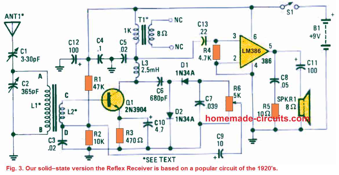 Our next TRF receiver's design, is depicted in the Fig.
3, and it is designed using the radio reflex circuit which used to be very popular during the 1920's.
In those days radio was merely seeing the trend and home built radio sets were being developed with tremendous enthusiasm by the experimenters.
Now take a look at how our present day solid-state transistorized version of the reflex receiver functions.
The RF signal is transferred through the antenna by means of C1 which reaches the tuned circuit consisting of L1 and C2.
One particular end of L2 supplies the RF signal to the transistor Q1 base so that the signal can be amplified, while the other end of L2 connects to the R1 and R2 junction to enable the biasing supply for the transistor.
The capacitor, C3, clamps the "D" end of L2 at RF ground.
Next, the amplified RF signal is fed via C6 to a two-diode doubler + detector circuit and then the signal is further sent to the the volume control stage using pot R6.
The central slider arm of the pot R6 connects with the detected audio signal via C9 to the R1, R2 junction and the "D" end of L2. The "D" end of L2 is held at the RF ground, which is not the AF ground.
This allows the AF signal to move by means of L2 towards the Q1 base for amplification.
The connection between the 2.5 mH choke and T1 is held at RF ground via the capacitor C5.
The amplified radio audio available from this stage is passed to the input of the LM386 IC audio amplifier, U1, for operating a 4 inch diameter 8 ohm loud speaker.
The single transistor perdorms a double function, it amplifies the RF and AM radio signals both together simulataneously.
The construction format which had been used for building our first receiver can be also applied here for building this reflex radio receiver circuit.
Inductors L1 and L2 are identical to those employed in the previous circuit and could be built by looking at the constructional details given in Fig.
2. When correctly put together, the reflex circuit will work exceptionally well even better than the first receiver by providing enhanced sensitivity and louder audio output.
Our next TRF receiver's design, is depicted in the Fig.
3, and it is designed using the radio reflex circuit which used to be very popular during the 1920's.
In those days radio was merely seeing the trend and home built radio sets were being developed with tremendous enthusiasm by the experimenters.
Now take a look at how our present day solid-state transistorized version of the reflex receiver functions.
The RF signal is transferred through the antenna by means of C1 which reaches the tuned circuit consisting of L1 and C2.
One particular end of L2 supplies the RF signal to the transistor Q1 base so that the signal can be amplified, while the other end of L2 connects to the R1 and R2 junction to enable the biasing supply for the transistor.
The capacitor, C3, clamps the "D" end of L2 at RF ground.
Next, the amplified RF signal is fed via C6 to a two-diode doubler + detector circuit and then the signal is further sent to the the volume control stage using pot R6.
The central slider arm of the pot R6 connects with the detected audio signal via C9 to the R1, R2 junction and the "D" end of L2. The "D" end of L2 is held at the RF ground, which is not the AF ground.
This allows the AF signal to move by means of L2 towards the Q1 base for amplification.
The connection between the 2.5 mH choke and T1 is held at RF ground via the capacitor C5.
The amplified radio audio available from this stage is passed to the input of the LM386 IC audio amplifier, U1, for operating a 4 inch diameter 8 ohm loud speaker.
The single transistor perdorms a double function, it amplifies the RF and AM radio signals both together simulataneously.
The construction format which had been used for building our first receiver can be also applied here for building this reflex radio receiver circuit.
Inductors L1 and L2 are identical to those employed in the previous circuit and could be built by looking at the constructional details given in Fig.
2. When correctly put together, the reflex circuit will work exceptionally well even better than the first receiver by providing enhanced sensitivity and louder audio output.
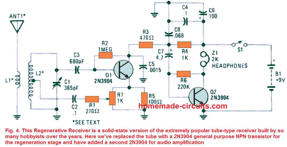 Our 3rd tuned radio frequency receiver circuit as shown in the Fig.
4 is a solid state version of the very famous old regenerative receiver which could have been built by numerous small radio makers through the years.
The main active part of the regenerative tuned radio frequency receiver circuits is the transistor 2N3904 configured for the regeneration stage, while the second 2N3904 is wired for the audio amplification.
In the diagram we can see that transistor Q1 is hooked up like a customized Hartley regenerative detector circuit having the RF feedback level determined by R7, which is a 1k potentiometer.
The RF is connected via L2 to L1 and tuned to the preferred frequency through the capacitor C1
Our 3rd tuned radio frequency receiver circuit as shown in the Fig.
4 is a solid state version of the very famous old regenerative receiver which could have been built by numerous small radio makers through the years.
The main active part of the regenerative tuned radio frequency receiver circuits is the transistor 2N3904 configured for the regeneration stage, while the second 2N3904 is wired for the audio amplification.
In the diagram we can see that transistor Q1 is hooked up like a customized Hartley regenerative detector circuit having the RF feedback level determined by R7, which is a 1k potentiometer.
The RF is connected via L2 to L1 and tuned to the preferred frequency through the capacitor C1
 This implementation provides a digitized output which is a lot more gratifying to hear and might even turn an unclear distorted digitization into something which may be a lot more attractive to hear.
By simply applying the dithering method, a 1 bit, 10-kHz sample can reach through an absolute rubbish to a well-known figure.
The miracle range for noise input is approximately 70% of 1 bit.
This means that , if you apply an input of 8 bits with a input signal of 2 V peak-to-peak, the noise level to be induced will be:
Vnoise = Vinp-p / 2n bits x 0.7
Vnoise = Vinp-p / 28x 0.7
Vnoise = 2 / 256 x 0.7
Vnoise = 5.5 mV
This implementation provides a digitized output which is a lot more gratifying to hear and might even turn an unclear distorted digitization into something which may be a lot more attractive to hear.
By simply applying the dithering method, a 1 bit, 10-kHz sample can reach through an absolute rubbish to a well-known figure.
The miracle range for noise input is approximately 70% of 1 bit.
This means that , if you apply an input of 8 bits with a input signal of 2 V peak-to-peak, the noise level to be induced will be:
Vnoise = Vinp-p / 2n bits x 0.7
Vnoise = Vinp-p / 28x 0.7
Vnoise = 2 / 256 x 0.7
Vnoise = 5.5 mV
 Rferring to the circuit shown in Fig.
2, we can observe that the configuration using capacitors C1 --- C3, transistors Q1, Q2, and resistors R1-----R4 form a pink-noise generator circuit.
Transistor Q1 is hooked up like a reverse-biased diode junction, and is accustomed to crank out a white-noise (haphazard noise) signal.
That white noise signal is capacitively coupled to the base of Q2 through C1. Transistor Q2 amplifies the noise signal.
The Q2 output is applied to C2, for eliminating for for filtering out the higher frequencies tso that it replicates pink noise far more strongly.
Parts C4, U1, U2, and R5-R14 are configured to form an audio- amplifier/noiseamplifier/mixer circuit respectively.
The noise generator output is adequately high for serving the intended functions and this only needs some buffering, that's all.
The filtered pink-noise signal is supplied by means of C3 and R5 to the inverting input of U1, which generates an boosted and an inverted replication of the input audio signal.
Op-amp U2, in association with resistors R12 and R8 are put together to provide a optimum gain of 100, getting rid of an extra preamp stage before the digitizer.
The output of U1 and U2 merge at the junction of R14 and C4, and are the finalized enhanced super digitized audio is supplied circuit's output jacks.
Rferring to the circuit shown in Fig.
2, we can observe that the configuration using capacitors C1 --- C3, transistors Q1, Q2, and resistors R1-----R4 form a pink-noise generator circuit.
Transistor Q1 is hooked up like a reverse-biased diode junction, and is accustomed to crank out a white-noise (haphazard noise) signal.
That white noise signal is capacitively coupled to the base of Q2 through C1. Transistor Q2 amplifies the noise signal.
The Q2 output is applied to C2, for eliminating for for filtering out the higher frequencies tso that it replicates pink noise far more strongly.
Parts C4, U1, U2, and R5-R14 are configured to form an audio- amplifier/noiseamplifier/mixer circuit respectively.
The noise generator output is adequately high for serving the intended functions and this only needs some buffering, that's all.
The filtered pink-noise signal is supplied by means of C3 and R5 to the inverting input of U1, which generates an boosted and an inverted replication of the input audio signal.
Op-amp U2, in association with resistors R12 and R8 are put together to provide a optimum gain of 100, getting rid of an extra preamp stage before the digitizer.
The output of U1 and U2 merge at the junction of R14 and C4, and are the finalized enhanced super digitized audio is supplied circuit's output jacks.
 Once the pcb is etched out you may start procuring the parts, and then start the construction work.
Begin by soldering the IC sockets around the areas as pointed out in Fig.
4. Next, assemble and solder all the components on the PCB accordingly.
Ensure that all components that have polarity are installed using the appropriate direction.
You can incorporate RCA-type phono jacks for the audio input and output.
Once the pcb is etched out you may start procuring the parts, and then start the construction work.
Begin by soldering the IC sockets around the areas as pointed out in Fig.
4. Next, assemble and solder all the components on the PCB accordingly.
Ensure that all components that have polarity are installed using the appropriate direction.
You can incorporate RCA-type phono jacks for the audio input and output.


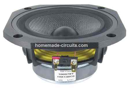 The HT210F0 bass and HT130F0 were intended to be employed collectively, which us substantiated by their meticulously matched up reference efficiencies.
These may also be available in pairs, computer matched to within <0.3dB, to ensure that gain matching can be avoided.
Developing a good speaker system can eliminate the several, usually mutually interconnected issues for getting an impressive bass effect with smaller speaker boxes.
At best, the specific responses of the cross over drivers employed in this circuit work exactly like the asymmetrical band-pass filters, using unnecessary resonances chucked in.
These types of effects requires to be altered and tamed in order that the system response is similar to a band-pass filter having a toned output throughout the acoustic frequency range.
One of the many approaches employed was an easy treble response and precise incorporation of driver responses.
After working with a number of tweeters units, such as titanium and hard-dome types, I decided to go with the Morel MDT29, a soft-dome unit having a fantastic, sleek and resonance-free effect coupled with a likewise soft low-frequency roll-off.
The HT210F0 bass and HT130F0 were intended to be employed collectively, which us substantiated by their meticulously matched up reference efficiencies.
These may also be available in pairs, computer matched to within <0.3dB, to ensure that gain matching can be avoided.
Developing a good speaker system can eliminate the several, usually mutually interconnected issues for getting an impressive bass effect with smaller speaker boxes.
At best, the specific responses of the cross over drivers employed in this circuit work exactly like the asymmetrical band-pass filters, using unnecessary resonances chucked in.
These types of effects requires to be altered and tamed in order that the system response is similar to a band-pass filter having a toned output throughout the acoustic frequency range.
One of the many approaches employed was an easy treble response and precise incorporation of driver responses.
After working with a number of tweeters units, such as titanium and hard-dome types, I decided to go with the Morel MDT29, a soft-dome unit having a fantastic, sleek and resonance-free effect coupled with a likewise soft low-frequency roll-off.
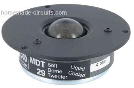 Additionally, it is a sturdy ferro fluid-cooled device competent to handle high power transients.
It is currently clearly recognized that a wide stereo visuals demands decent horizontal audio distribution.
This calls for a narrow speaker box, and to achieve the smallest front side baffle measurements, the bass driver is clamped on the edge of the speaker box.
This actually does not trigger any complications, since below 100 Hz frequency, the response from the bass driver is over a single direction.
Additionally, it is a sturdy ferro fluid-cooled device competent to handle high power transients.
It is currently clearly recognized that a wide stereo visuals demands decent horizontal audio distribution.
This calls for a narrow speaker box, and to achieve the smallest front side baffle measurements, the bass driver is clamped on the edge of the speaker box.
This actually does not trigger any complications, since below 100 Hz frequency, the response from the bass driver is over a single direction.
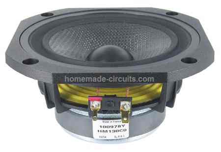 The mid-range driver requires its very own housing.
In a three-way crossover models, it is a widespread approach to attach this sub-enclosure inside the primary speaker box and, after many hours of deep thinking, I selected a garden 6in diameter terracotta flower pot.
The mid-range driver requires its very own housing.
In a three-way crossover models, it is a widespread approach to attach this sub-enclosure inside the primary speaker box and, after many hours of deep thinking, I selected a garden 6in diameter terracotta flower pot.
 Despite the fact that the preference may look unusual, the non-parallel design means that, around the mid driver's range, vertical sound waves are not able to happen inside the sub-enclosure.
Fitted in this manner, the HT130FO's bass resonance is increased from 48 Hz to 144 Hz, through a accompanying rise in Q from 0.25 to roughly 0.73, the healthy selection for the crossover point across the mid-range and bass drivers.
Enabling the roll-off for the bass unit with this frequency additionally means that the speaker box is acoustically compact and much smaller.
In other words, the wavelengths of the audio supplied through the driver are much much longer compared to biggest speaker box available.
Consequently, standing waves can't be created inside it.
Despite the fact that the preference may look unusual, the non-parallel design means that, around the mid driver's range, vertical sound waves are not able to happen inside the sub-enclosure.
Fitted in this manner, the HT130FO's bass resonance is increased from 48 Hz to 144 Hz, through a accompanying rise in Q from 0.25 to roughly 0.73, the healthy selection for the crossover point across the mid-range and bass drivers.
Enabling the roll-off for the bass unit with this frequency additionally means that the speaker box is acoustically compact and much smaller.
In other words, the wavelengths of the audio supplied through the driver are much much longer compared to biggest speaker box available.
Consequently, standing waves can't be created inside it.
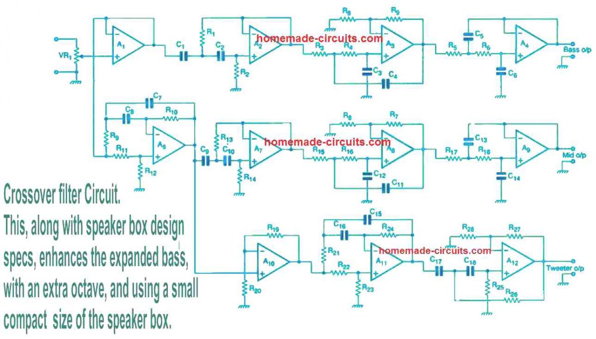 The line-level inputs are put on the volume control VR1 and subsequently on the buffer amplifier constructed using A1. After this the audio frequency is bifurcated across three sections.
Amplifier A2 is set up like a high-pass filter which has a turnover frequency of 28 Hz and a Q of 2.82, principally to deliver bass equalization for the woofer.
Bass frequency loading is done at the 6th order and the bass speaker box is tuned with a low frequency of 35 Hz.
This low frequency generates an overdamped 4th order filter effect.
Low frequency boost implemented through op amp A2 flattens the response, guaranteeing a -3dB point for the speaker system at 32 Hz.
Reflex type speaker units are generally not loaded acoustically at subsonic frequencies and, while in traditional speaker systems, the driver excursion is sacrificed through subsonic interference.
A well-defined filter roll-off makes certain that subsonic frequencies are adequately attenuated in order to prevent overloading.
Initiatives to force the effect lower than this frequency level causes excursion limit complications.
Crossovers between the bass and mid-range drivers stages is taken care of by op amps A3 and A4, which work like a 4th-order, low-pass filter using a couple of 2nd-order sections.
Q of the final filter can be 0.5, the situation of crucial damping merging the most effective transient response along with fast stop-band attenuation.
Properties of the mid-range enclosure determine the selection of crossover point.
The midrange driver, rolls off at the bass frequency last limit at 144Hz, generating a very similar effect like a 2nd-order filter having a turnover frequency of 144 Hz and a Q of 0.73.
By itself, the high Q of this resonance might produce an adverse peak slightly over the resonant frequency.
To keep the response under control the drive signal is subjected to a high-pass filter through the op amp A7, that provides an identical turnover frequency although with a Q of 0.68. The audio effect generated due to this is equivalent to the intended 4th-order high-pass crossover response.
Due to the fact the driver's audible zones are located in distinctive planes, time delay utilizing all-pass filters is necessary for the compensations.
(This noticeable contradiction in conditions is enforced to circuits that offer a flat frequency response although a predetermined time delay.)
A couple of these filters are employed in the circuit.
The 1st, constructed using the op amp A6 offsets the time delay between the woofer and mid-range units.
This is similar to, a -24ˇă phase shift at 144 Hz.
The 2nd offsets the time delay between mid range and tweeter.
Here a -50 mm offset is adjusted by op amp A11 and the involved circuitry.
The line-level inputs are put on the volume control VR1 and subsequently on the buffer amplifier constructed using A1. After this the audio frequency is bifurcated across three sections.
Amplifier A2 is set up like a high-pass filter which has a turnover frequency of 28 Hz and a Q of 2.82, principally to deliver bass equalization for the woofer.
Bass frequency loading is done at the 6th order and the bass speaker box is tuned with a low frequency of 35 Hz.
This low frequency generates an overdamped 4th order filter effect.
Low frequency boost implemented through op amp A2 flattens the response, guaranteeing a -3dB point for the speaker system at 32 Hz.
Reflex type speaker units are generally not loaded acoustically at subsonic frequencies and, while in traditional speaker systems, the driver excursion is sacrificed through subsonic interference.
A well-defined filter roll-off makes certain that subsonic frequencies are adequately attenuated in order to prevent overloading.
Initiatives to force the effect lower than this frequency level causes excursion limit complications.
Crossovers between the bass and mid-range drivers stages is taken care of by op amps A3 and A4, which work like a 4th-order, low-pass filter using a couple of 2nd-order sections.
Q of the final filter can be 0.5, the situation of crucial damping merging the most effective transient response along with fast stop-band attenuation.
Properties of the mid-range enclosure determine the selection of crossover point.
The midrange driver, rolls off at the bass frequency last limit at 144Hz, generating a very similar effect like a 2nd-order filter having a turnover frequency of 144 Hz and a Q of 0.73.
By itself, the high Q of this resonance might produce an adverse peak slightly over the resonant frequency.
To keep the response under control the drive signal is subjected to a high-pass filter through the op amp A7, that provides an identical turnover frequency although with a Q of 0.68. The audio effect generated due to this is equivalent to the intended 4th-order high-pass crossover response.
Due to the fact the driver's audible zones are located in distinctive planes, time delay utilizing all-pass filters is necessary for the compensations.
(This noticeable contradiction in conditions is enforced to circuits that offer a flat frequency response although a predetermined time delay.)
A couple of these filters are employed in the circuit.
The 1st, constructed using the op amp A6 offsets the time delay between the woofer and mid-range units.
This is similar to, a -24ˇă phase shift at 144 Hz.
The 2nd offsets the time delay between mid range and tweeter.
Here a -50 mm offset is adjusted by op amp A11 and the involved circuitry.
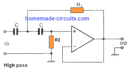 Part values for the high-pass system could be calculated through the below given equations.
R2 = a/(1.257 x 10-6foC), select a value for the C that is suitable to you.
R1 = 1 / (3.142 x 10⁻⁶afoC), where a = 1/Q, and C is expressed in microfrarads (uF)
Part values for the high-pass system could be calculated through the below given equations.
R2 = a/(1.257 x 10-6foC), select a value for the C that is suitable to you.
R1 = 1 / (3.142 x 10⁻⁶afoC), where a = 1/Q, and C is expressed in microfrarads (uF)
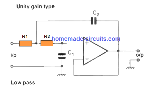 Select the value for R that is most convenient for you, then:
C1 = a/(12.57foR)
C2 = 1/(3.142afoR)
fo is the intended cut-off transition frequency
The Q of the filter is established through the voltage gain of the circuit, which is fixed through the ratio of R3 and R4.
R3 needs to be (3-(1/Q+1))R4. Higher order filters can be attained by cascading 2nd-order filters; the Q of a cascaded pair can be equal to the product of the Qs of each segment.
The following graph demonstrates the result of Q over the response curve of a 2nd-order filter, which is a high-pass type here.
Select the value for R that is most convenient for you, then:
C1 = a/(12.57foR)
C2 = 1/(3.142afoR)
fo is the intended cut-off transition frequency
The Q of the filter is established through the voltage gain of the circuit, which is fixed through the ratio of R3 and R4.
R3 needs to be (3-(1/Q+1))R4. Higher order filters can be attained by cascading 2nd-order filters; the Q of a cascaded pair can be equal to the product of the Qs of each segment.
The following graph demonstrates the result of Q over the response curve of a 2nd-order filter, which is a high-pass type here.
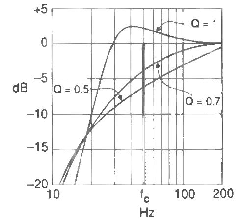 The effect of low-pass filters can be a preciely identical image.
Underdamped filters of Q>0.7 indicate a peak in the passband, while this cannot be seen in overdamped filters having Q<0.7.
Filters with a Q of 0.7 are Butterworth types, that enjoy the flattest passband response along with zero peak.
Nevertheless, it could be proven that most effective transient response can be acquired with a Q of 0.5, irrespective of filter order; therefore this value has been the most popular Q of crossovers.
The regular Linkwitz/Riley crossover works with a 4th-order filter for both high and low-pass segments.
An additional good thing about the 4th-order filter is usually that the phase difference between the sections is minimal.
The effect of low-pass filters can be a preciely identical image.
Underdamped filters of Q>0.7 indicate a peak in the passband, while this cannot be seen in overdamped filters having Q<0.7.
Filters with a Q of 0.7 are Butterworth types, that enjoy the flattest passband response along with zero peak.
Nevertheless, it could be proven that most effective transient response can be acquired with a Q of 0.5, irrespective of filter order; therefore this value has been the most popular Q of crossovers.
The regular Linkwitz/Riley crossover works with a 4th-order filter for both high and low-pass segments.
An additional good thing about the 4th-order filter is usually that the phase difference between the sections is minimal.
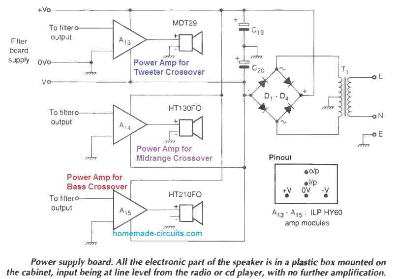 Parts List
 However, the disadvantage of using a piezo as a sensor is that, when you use wood or harder drumstick material, the piezo disc can break and there is no longer any beat.
We have two circuits for this drum sound experiment.
Our first one will resolve the issue of the piezo sensor as well as lay a thicker material for more robust usage.
Even when you use a typical ceramic disc capacitor and attempt a few beats, you can still detect an output based on the drum beats.
However, the disadvantage of using a piezo as a sensor is that, when you use wood or harder drumstick material, the piezo disc can break and there is no longer any beat.
We have two circuits for this drum sound experiment.
Our first one will resolve the issue of the piezo sensor as well as lay a thicker material for more robust usage.
Even when you use a typical ceramic disc capacitor and attempt a few beats, you can still detect an output based on the drum beats.
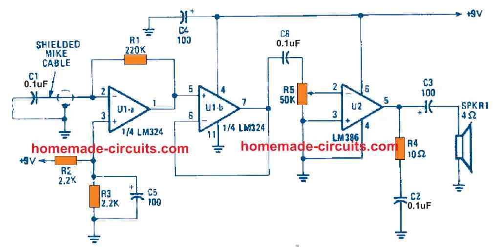 Parts List
 The schematic in Figure 1 shown above is an excellent test circuit because it allows you to hear the audible tone of each capacitor as you check them.
There are some capacitors which generate a short ˇ°pingingˇ± drum beat sound whereas other have significant and longer ringing sound.
The schematic in Figure 1 shown above is an excellent test circuit because it allows you to hear the audible tone of each capacitor as you check them.
There are some capacitors which generate a short ˇ°pingingˇ± drum beat sound whereas other have significant and longer ringing sound.
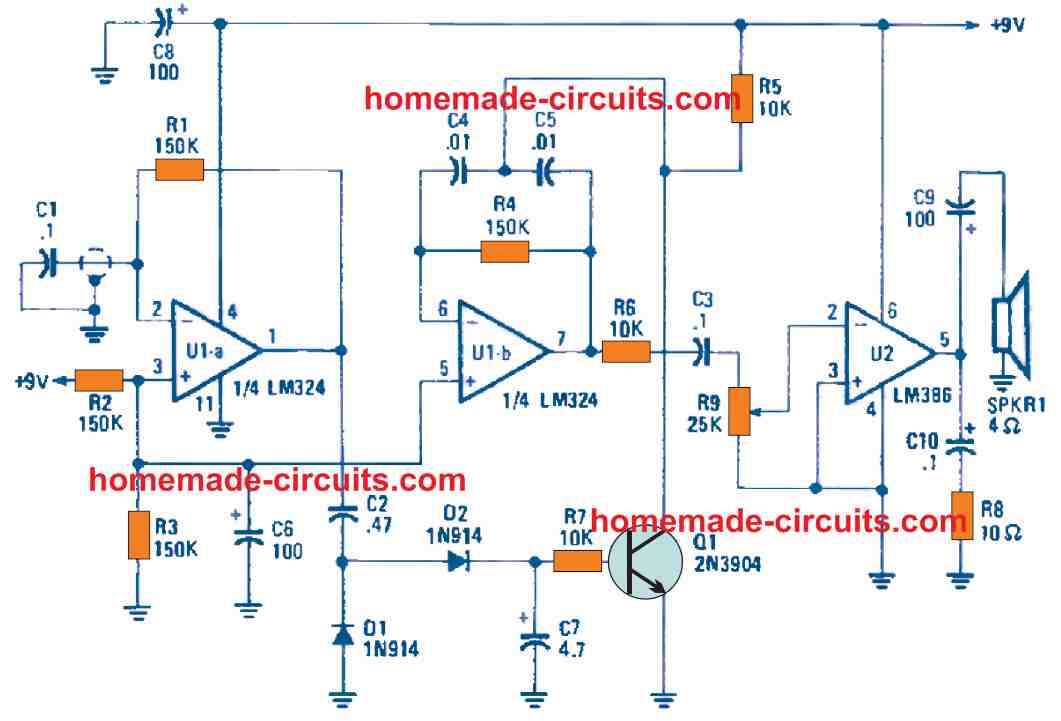 Parts List
 Percussion tools and other musical audio including bongos, drums, wood blocks, gongs are perhaps the most well-known to all of us.
These musical special effect generators tend to be very appealing and complement to most contemporary music.
The Hi-Fi, depth, and tempo these types of musical sounds induce upon nearly every form of music is genuinely worth listening to and appreciated.
Percussion tools and other musical audio including bongos, drums, wood blocks, gongs are perhaps the most well-known to all of us.
These musical special effect generators tend to be very appealing and complement to most contemporary music.
The Hi-Fi, depth, and tempo these types of musical sounds induce upon nearly every form of music is genuinely worth listening to and appreciated.
 This electronic bongo project creates a perfect add - on to any existing amplifier system.
All the 5 unique sounds generated by this circuit is produced by specific twin-tee ringing oscillator stages.
(A ringing oscillator is not really a free-running astable, rather could be activated or shot into a quick burst of oscillation by any form of spiked or pulse.)
Considering that our body builds up a certain electric charge, the oscillators are set off by simply tapping the given touch-plates using your fingers.
Therefore the device could be operated in a way much like authentic bongos instruments.
Making this above discussed bongo circuit is actually very easy, and just aboiuut assembling the indicated parts over a stripboard.
The final output could be then extracted through a 3.5 mm jack into any audio amplifier for getting the hi-fi, enhanced electronic bongo sound over a suitable loudspeaker.
The 5 presets could be tweaked appropriately for adjusting and trimming the bongo sounds as per personal taste and preference.
This electronic bongo project creates a perfect add - on to any existing amplifier system.
All the 5 unique sounds generated by this circuit is produced by specific twin-tee ringing oscillator stages.
(A ringing oscillator is not really a free-running astable, rather could be activated or shot into a quick burst of oscillation by any form of spiked or pulse.)
Considering that our body builds up a certain electric charge, the oscillators are set off by simply tapping the given touch-plates using your fingers.
Therefore the device could be operated in a way much like authentic bongos instruments.
Making this above discussed bongo circuit is actually very easy, and just aboiuut assembling the indicated parts over a stripboard.
The final output could be then extracted through a 3.5 mm jack into any audio amplifier for getting the hi-fi, enhanced electronic bongo sound over a suitable loudspeaker.
The 5 presets could be tweaked appropriately for adjusting and trimming the bongo sounds as per personal taste and preference.
 When this delayed signal is fed back (recirculated) into the original signal, a reverberation effect is simulated.
Besides delivering real-time ambiance, the bucket-brigade circuit could be implemented with any audio system to produce synthetic stereo sound from mono audio sources, an useful option for "double voicing," and "phasor/flanging."
When this delayed signal is fed back (recirculated) into the original signal, a reverberation effect is simulated.
Besides delivering real-time ambiance, the bucket-brigade circuit could be implemented with any audio system to produce synthetic stereo sound from mono audio sources, an useful option for "double voicing," and "phasor/flanging."
 The above image is a schematic manifestation of 4 standard stages of the MN3001 analog shift register.
Each MN3001 IC consists of two 512 -stage shift registers.
Remember that stages A and C are linked to one particular clock, while stages B and D are coupled to the other clock to deliver the odd/even relationship.
The above image is a schematic manifestation of 4 standard stages of the MN3001 analog shift register.
Each MN3001 IC consists of two 512 -stage shift registers.
Remember that stages A and C are linked to one particular clock, while stages B and D are coupled to the other clock to deliver the odd/even relationship.
 When you actually create a delay in an audio signal, you generate a variety of interesting audio effects.
The most noticeable is the simulation of echo effect.
However, delays created by the bucket brigade are usually very small to be recognized as discrete echoes.
Repeating the delayed signal with diminished gain could mimic the healthy decay of echoes in a reverberant space.
By introducing certain gain throughout the re-circulation of the delayed signal, it may be possible to generate an unnatural "door-spring" outcome for the music.
Causing delay to an instrumental signal or speech track by 30 or 40 ms and pushing the delayed signal back to the original signal, will produce the output audio more voluminous and provide it the impression of having more than the initial quantity of voices or musical depth.
This kind of popular approach is called "double-voicing." Another well-known short-delay effect can be in the form of a peculiar sound that arises through a technique called "phasing" or "reel-flanging."
The title comes from its original experimentation in which a tape recorder had been employed to generate the time delay, and the rubbing of a skilled hand on the outer side of the tape-feed reel altered the delay to generate the acoustic effect.
Today, this effect could be developed entirely through digital technology, by delaying the signal 0.5 to 5 ms while adding or subtracting the delayed signal from the original signal.
In the phasor/flanger setting, the frequency and its harmonics whose wavelengths are identical to the time delay, happens to be fully terminated, while all the other frequencies become strengthened.
In this manner a comb filter having a frequency between the notches is modified by changing the clock frequency, as shown below.
When you actually create a delay in an audio signal, you generate a variety of interesting audio effects.
The most noticeable is the simulation of echo effect.
However, delays created by the bucket brigade are usually very small to be recognized as discrete echoes.
Repeating the delayed signal with diminished gain could mimic the healthy decay of echoes in a reverberant space.
By introducing certain gain throughout the re-circulation of the delayed signal, it may be possible to generate an unnatural "door-spring" outcome for the music.
Causing delay to an instrumental signal or speech track by 30 or 40 ms and pushing the delayed signal back to the original signal, will produce the output audio more voluminous and provide it the impression of having more than the initial quantity of voices or musical depth.
This kind of popular approach is called "double-voicing." Another well-known short-delay effect can be in the form of a peculiar sound that arises through a technique called "phasing" or "reel-flanging."
The title comes from its original experimentation in which a tape recorder had been employed to generate the time delay, and the rubbing of a skilled hand on the outer side of the tape-feed reel altered the delay to generate the acoustic effect.
Today, this effect could be developed entirely through digital technology, by delaying the signal 0.5 to 5 ms while adding or subtracting the delayed signal from the original signal.
In the phasor/flanger setting, the frequency and its harmonics whose wavelengths are identical to the time delay, happens to be fully terminated, while all the other frequencies become strengthened.
In this manner a comb filter having a frequency between the notches is modified by changing the clock frequency, as shown below.
 The result is, a tonal improvement introduced to a non-tonal audio, for example drums, cymbals, as well as to vocal frequencies.
The phasor/flanger mode enables you to replicate stereophonic signals from a monophonic origin.
To achieve this, the phased output extracted by introducing the delayed signal is sent to one channel, while the output extracted by subtracting the delayed signal is sent to the opposite.
For the audience, the phasing effect cancels out, allowing a good synthetic stereo effect to their ears.
The main elements of the designs, undoubtedly, are the bucket-brigade IC's, that are able to directly synthesize the analog signals.
The circuits do not involve expensive analog-to-digital and digital-to-analog converters.
As soon as the clock pulse from the flipflop is fed to the bucket-brigade IC, the DC supply existing at the input is transferred into the register.
The discrete bits are shifted stage by stage through sequential clock pulses until eventually, after 256 pulses, they arrive at the finish of the line and deliver the output signal.
The output waveform is cleaned up with a low-pass filter and whatever duplicate signal had been existing at the input but delayed by 256 times the period of the clock frequency.
For instance, when the clock frequency is 100 kHz, the delay could be 256 x 1/100,000 = 2.56 ms.
Considering that the sampling rate of the music signal on the input is dependent on the clock frequency, an assumptive limit of 50% lower clock frequency could be the maximum audio frequency which can be effectively transferred.
Nevertheless, because of real life constraints, 1/3rd of the clock frequency may appear to be a more realistic design objective.
Circuits could be sequentially connected or cascaded to offer lengthier time delays at increased clock rates, though the higher noise in the series-connected circuits may possibly outdo the rise in the bandwidth.
In the delay mode, the 2 shift registers are hooked up in series, which enables the use of clock frequencies two times higher.
This allows, two times the bandwidth for each shift register to be programmed for the very same time delay.
Even in this double-bandwidth mode, the clock frequency necessary for a 40 ms delay, restricts the bandwidth to a maximum input signal of 3750 Hz, which looks quite enough for voice frequency, although not enough for most musical equipment.
In many applications in which the delayed transmission is implemented to the original signal, the decrease in bandwidth can get concealed due to the high-frequency signals contained in the original signal input.
To compensate for normal signal attenuation, an 8.5 dB amplifier is employed between the shift registers.
In the phasor/flanger mode, the highest delay necessary is approximately 5 ms, which is small enough for the use of a single shift register without sacrificing the bandwidth.
The second shift register is consequently attached in parallel with the first to enhance the S/N ratio.
The signal frequencies are applied in-phase, while the noise signals get added and deducted at random.
The result is, a tonal improvement introduced to a non-tonal audio, for example drums, cymbals, as well as to vocal frequencies.
The phasor/flanger mode enables you to replicate stereophonic signals from a monophonic origin.
To achieve this, the phased output extracted by introducing the delayed signal is sent to one channel, while the output extracted by subtracting the delayed signal is sent to the opposite.
For the audience, the phasing effect cancels out, allowing a good synthetic stereo effect to their ears.
The main elements of the designs, undoubtedly, are the bucket-brigade IC's, that are able to directly synthesize the analog signals.
The circuits do not involve expensive analog-to-digital and digital-to-analog converters.
As soon as the clock pulse from the flipflop is fed to the bucket-brigade IC, the DC supply existing at the input is transferred into the register.
The discrete bits are shifted stage by stage through sequential clock pulses until eventually, after 256 pulses, they arrive at the finish of the line and deliver the output signal.
The output waveform is cleaned up with a low-pass filter and whatever duplicate signal had been existing at the input but delayed by 256 times the period of the clock frequency.
For instance, when the clock frequency is 100 kHz, the delay could be 256 x 1/100,000 = 2.56 ms.
Considering that the sampling rate of the music signal on the input is dependent on the clock frequency, an assumptive limit of 50% lower clock frequency could be the maximum audio frequency which can be effectively transferred.
Nevertheless, because of real life constraints, 1/3rd of the clock frequency may appear to be a more realistic design objective.
Circuits could be sequentially connected or cascaded to offer lengthier time delays at increased clock rates, though the higher noise in the series-connected circuits may possibly outdo the rise in the bandwidth.
In the delay mode, the 2 shift registers are hooked up in series, which enables the use of clock frequencies two times higher.
This allows, two times the bandwidth for each shift register to be programmed for the very same time delay.
Even in this double-bandwidth mode, the clock frequency necessary for a 40 ms delay, restricts the bandwidth to a maximum input signal of 3750 Hz, which looks quite enough for voice frequency, although not enough for most musical equipment.
In many applications in which the delayed transmission is implemented to the original signal, the decrease in bandwidth can get concealed due to the high-frequency signals contained in the original signal input.
To compensate for normal signal attenuation, an 8.5 dB amplifier is employed between the shift registers.
In the phasor/flanger mode, the highest delay necessary is approximately 5 ms, which is small enough for the use of a single shift register without sacrificing the bandwidth.
The second shift register is consequently attached in parallel with the first to enhance the S/N ratio.
The signal frequencies are applied in-phase, while the noise signals get added and deducted at random.
 The schematic diagram for the phasor/flanger is given below:
 In each scenarios, quad NOR gate IC4 is rigged like astable multivibrator functioning at two times the specified clock rate's frequency.
The IC4 output connects with flip-flop IC5, that offers a couple of contributory (180ˇă out of phase with each other) output clock signals with FIFTY PERCENT duty cycles.
These pulses then act as clock inputs for the shift registers in IC2. Resistor R16 determines the frequency and is a fixed velue in the delay circuit.
The clock frequency could be changed as desired by adding more resistors in parallel through the given connectors in the phasor/flanger.
The audio input signal is processed through seven poles of low-pass filter stages, where IC3 and 1/2 IC1 are utilized.
The filters ensure an overall attenuation of 42-dB/octave over a tuned frequency.
As an illustration, when the filter is tuned for 5000 Hz, a 10,000 Hz signal gets attenuated by greater than 100:1.
While the filters are operated with high-gain op amps, you are able to make their outputs maximize before rolling off at 6 dB/octave rate per pole.
This kind of filters are called "under damped."
Through proper selection of the balance of under-damped and over-damped (RC) filter stages, it is easy to configure a filter having a flat response in the intended passband, in order to achive 3 dB down on the tuning frequency, and feature a roll-off rate of 6 dB times the quantity of poles.
This is exactly what is implemented in the delay-line and phasor/flanger designs presented in this article.
A substantial amount of statistical working out is usually needed to identify the resistor values for the filters.
To make things easier, you could pick out the suitable resistor values from the Table of Filter Resistor Values.
In each scenarios, quad NOR gate IC4 is rigged like astable multivibrator functioning at two times the specified clock rate's frequency.
The IC4 output connects with flip-flop IC5, that offers a couple of contributory (180ˇă out of phase with each other) output clock signals with FIFTY PERCENT duty cycles.
These pulses then act as clock inputs for the shift registers in IC2. Resistor R16 determines the frequency and is a fixed velue in the delay circuit.
The clock frequency could be changed as desired by adding more resistors in parallel through the given connectors in the phasor/flanger.
The audio input signal is processed through seven poles of low-pass filter stages, where IC3 and 1/2 IC1 are utilized.
The filters ensure an overall attenuation of 42-dB/octave over a tuned frequency.
As an illustration, when the filter is tuned for 5000 Hz, a 10,000 Hz signal gets attenuated by greater than 100:1.
While the filters are operated with high-gain op amps, you are able to make their outputs maximize before rolling off at 6 dB/octave rate per pole.
This kind of filters are called "under damped."
Through proper selection of the balance of under-damped and over-damped (RC) filter stages, it is easy to configure a filter having a flat response in the intended passband, in order to achive 3 dB down on the tuning frequency, and feature a roll-off rate of 6 dB times the quantity of poles.
This is exactly what is implemented in the delay-line and phasor/flanger designs presented in this article.
A substantial amount of statistical working out is usually needed to identify the resistor values for the filters.
To make things easier, you could pick out the suitable resistor values from the Table of Filter Resistor Values.
 Take advantage of this Table for choosing resistor values specifically for the delay-line circuit.
(The filter resistor values given in Fig.
4 and its associated Bill of materials will give you an enhanced 5 ms delay, with the output 3 dB down at 15 kHz for the phasor/flanger.)
Take advantage of this Table for choosing resistor values specifically for the delay-line circuit.
(The filter resistor values given in Fig.
4 and its associated Bill of materials will give you an enhanced 5 ms delay, with the output 3 dB down at 15 kHz for the phasor/flanger.)
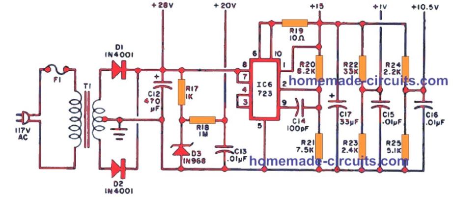 Parts List
C12 - 470 ¦ĚF, 35 V
C13,C15,C16 - 0.01 uF disc capacitor, C14 -100 pF disc capacitor
C17 - 33 ¦ĚF, 25 V
D1,D2 - IN4007
D3 -1N968 (20 V) zener diode
F1 -1/10 -ampere fuse
IC6 -723 precision voltage regulator
All resistors are I/4 watt 5% tolerance:
R17-1k
R18 - 1M
RI9 - 10 ohms
R20 - 8.2k ohms
R21 - 7.5k ohms
R22 - 33k ohms
R23 - 2.4k
The power supply circuit for the audio delay line is shown in the above image.
It is built around a voltage regulator, IC6, to crank out the primary 15 volt supply output.
The shift register involves sources of each +1 and +20 volts.
The +20 volt rail is acquired by using zener diode D3, and the +1 volt line comes from the voltage divider configured around R22 and R23.
As the op amps are driven through a single-ended supply, it becomes essential to have the 10.5 volt voltage line function as the reference in the circuit for these devices.
Parts List
C12 - 470 ¦ĚF, 35 V
C13,C15,C16 - 0.01 uF disc capacitor, C14 -100 pF disc capacitor
C17 - 33 ¦ĚF, 25 V
D1,D2 - IN4007
D3 -1N968 (20 V) zener diode
F1 -1/10 -ampere fuse
IC6 -723 precision voltage regulator
All resistors are I/4 watt 5% tolerance:
R17-1k
R18 - 1M
RI9 - 10 ohms
R20 - 8.2k ohms
R21 - 7.5k ohms
R22 - 33k ohms
R23 - 2.4k
The power supply circuit for the audio delay line is shown in the above image.
It is built around a voltage regulator, IC6, to crank out the primary 15 volt supply output.
The shift register involves sources of each +1 and +20 volts.
The +20 volt rail is acquired by using zener diode D3, and the +1 volt line comes from the voltage divider configured around R22 and R23.
As the op amps are driven through a single-ended supply, it becomes essential to have the 10.5 volt voltage line function as the reference in the circuit for these devices.
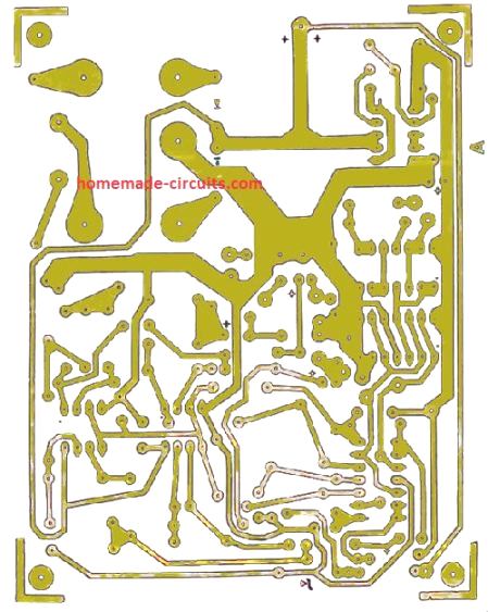
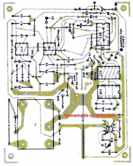 Prior to fitting any parts on the PCB, you should insert and solder the various jumpers links into the slots.
After that, connect the board as specified in above, according to the preferred mode of operation.
Be careful about the pin orientation of all the semiconductor devices and electrolytic capacitors, and insert them correctly.
Make sure to hold and assemble the MOS devices with care since these are sensitive to static charges, and may get damaged by the static charge developed on your fingers.
You could insert the IC's straight on the PCB or also make use of IC sockets.
Prior to fitting any parts on the PCB, you should insert and solder the various jumpers links into the slots.
After that, connect the board as specified in above, according to the preferred mode of operation.
Be careful about the pin orientation of all the semiconductor devices and electrolytic capacitors, and insert them correctly.
Make sure to hold and assemble the MOS devices with care since these are sensitive to static charges, and may get damaged by the static charge developed on your fingers.
You could insert the IC's straight on the PCB or also make use of IC sockets.
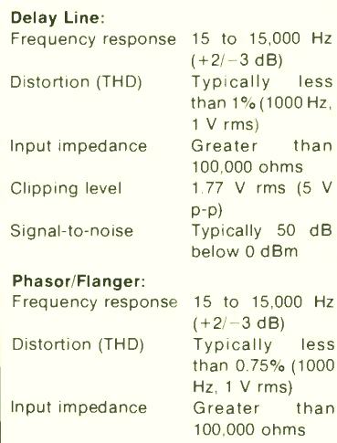
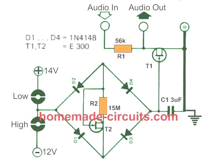 The FETs can be interchanged with any of these equivalents: BF256B, BF256C, BF348, BFT10A, 2N5397
The resistance formed across T1 is determined by the negative voltage created across capacitor C1.
When the touch pads associated with the negative supply line is contacted with finger, a current via D2, R2 and D3 charges the capacitor C1, with a delay time decided by the values of C1, R2.
When the negative charge developed across C1 is sufficiently high, T1 is inhibited from conducting anymore, which allows an un-attenuated audio signal to pass through.
This enables the volume to be increased
In order to reduce the volume of the audio, the user simply has to touch the pair of pads connected with the positive side of the supply.
This causes C1 to begin discharging, so that T1 again gets more conductive, and diverts the audio towards the ground line.
This causes a corresponding amount of attenuation on the audio signal, and the volume gets reduced proportionately.
The amount of volume to be attenuated or increased will depend on the time for how long the touch pads are kept contacted with the finger.
The FET T1 simply behaves like a linear resistor whose gate bias is modulated by the audio signal input.
The output distortion is reasonably low as long as the input audio signal is not exceeded 30 mV level.
The FETs can be interchanged with any of these equivalents: BF256B, BF256C, BF348, BFT10A, 2N5397
The resistance formed across T1 is determined by the negative voltage created across capacitor C1.
When the touch pads associated with the negative supply line is contacted with finger, a current via D2, R2 and D3 charges the capacitor C1, with a delay time decided by the values of C1, R2.
When the negative charge developed across C1 is sufficiently high, T1 is inhibited from conducting anymore, which allows an un-attenuated audio signal to pass through.
This enables the volume to be increased
In order to reduce the volume of the audio, the user simply has to touch the pair of pads connected with the positive side of the supply.
This causes C1 to begin discharging, so that T1 again gets more conductive, and diverts the audio towards the ground line.
This causes a corresponding amount of attenuation on the audio signal, and the volume gets reduced proportionately.
The amount of volume to be attenuated or increased will depend on the time for how long the touch pads are kept contacted with the finger.
The FET T1 simply behaves like a linear resistor whose gate bias is modulated by the audio signal input.
The output distortion is reasonably low as long as the input audio signal is not exceeded 30 mV level.

 The shown circuit diagram of the filter circuit associated with the drive units, features a cross-over frequency of 5kHz and roll-offs frequency of 12 dB per octave.
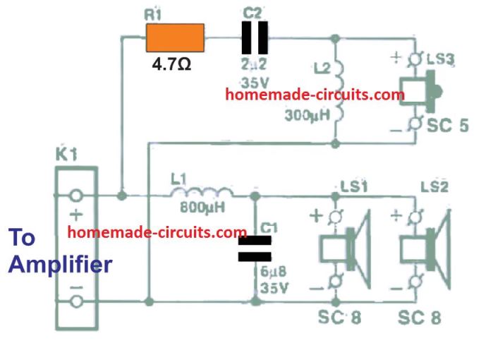 As a result of the shielding, the speaker could be positioned very close to a TV receiver, computer monitor or the preferred audio/video system.
Both 80 mm drive units are fitted at the lower half of the housing with the tweeter fitted above them.
As a result of the shielding, the speaker could be positioned very close to a TV receiver, computer monitor or the preferred audio/video system.
Both 80 mm drive units are fitted at the lower half of the housing with the tweeter fitted above them.
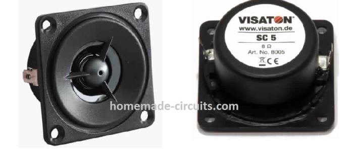 In several loudspeakers, the tweeter is positioned in between the two wideband units (also named as d'Appolito construction), however this includes the disadvantage that the waveform of sound radiation frequencies close to the cross-over frequency deviates substantially within the vertical direction (assuming the speaker is vertically positioned).
Generally, this may not have much impact on the sound, yet because the loudspeaker in surround-sound applications can often be listened to in resting position, could mean that audio frequency varying while the listener is moving his/her head a bit across right or left...
and this actually, may not be the ideal working of a surround sound.
In the proposed the construction this effect is simply eliminated, which means that sound stays homogeneous beyond the audible axis.
The efficiency of the Center 80 could be examined through the frequency characteristic in Figure 2
In several loudspeakers, the tweeter is positioned in between the two wideband units (also named as d'Appolito construction), however this includes the disadvantage that the waveform of sound radiation frequencies close to the cross-over frequency deviates substantially within the vertical direction (assuming the speaker is vertically positioned).
Generally, this may not have much impact on the sound, yet because the loudspeaker in surround-sound applications can often be listened to in resting position, could mean that audio frequency varying while the listener is moving his/her head a bit across right or left...
and this actually, may not be the ideal working of a surround sound.
In the proposed the construction this effect is simply eliminated, which means that sound stays homogeneous beyond the audible axis.
The efficiency of the Center 80 could be examined through the frequency characteristic in Figure 2
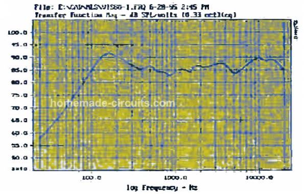
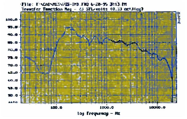 The roll-off at increased frequencies is triggered due to the basic reflections, as are indicated in the graph.
The 'normal' frequency curve, measured while the speaker were positioned horizontally down and radiating sound straight into the test microphone direction, could be witnessed in Figure 4.
The roll-off at increased frequencies is triggered due to the basic reflections, as are indicated in the graph.
The 'normal' frequency curve, measured while the speaker were positioned horizontally down and radiating sound straight into the test microphone direction, could be witnessed in Figure 4.
 The drive units could be secured by steel netting or covers.
The backside of each housing must have openings for the wire leads.
A few users could find it far easier to slice these holes prior to the box is nailed together.
Ensure that the cross-over filter is as stream-lined as it can be, as there is very little space inside the central speaker box.
A 15 mm hole could be chopped in one of the sides of the rear loudspeakers.
This allows a handy means of suspending the speakers from your wall (with the drive unit directing towards the roof).
The speaker boxes could be given a finishing touch as per personal flavor.
When everything is completed, the boxes could be wired up.
Each box must subsequently be stuffed with an appropriate damping substance, for example polyester wool or anything similar.
Parts List
The drive units could be secured by steel netting or covers.
The backside of each housing must have openings for the wire leads.
A few users could find it far easier to slice these holes prior to the box is nailed together.
Ensure that the cross-over filter is as stream-lined as it can be, as there is very little space inside the central speaker box.
A 15 mm hole could be chopped in one of the sides of the rear loudspeakers.
This allows a handy means of suspending the speakers from your wall (with the drive unit directing towards the roof).
The speaker boxes could be given a finishing touch as per personal flavor.
When everything is completed, the boxes could be wired up.
Each box must subsequently be stuffed with an appropriate damping substance, for example polyester wool or anything similar.
Parts List

 The Theremin works with a set of two high frequency oscillators for functioning.
One of these oscillators funtions with a constant frequency, while the other is variable through the body capacitance of the operator.
The frequency generated from the two oscillators are combined through an exclusive circuit called the balanced modulator.
The balanced modulator attenuates the initial signals and generates a complicated transmission which includes the sum and difference frequencies in the two inputs.
When one particular oscillator is performing at 100 kHz and the second one at 101 kHz, we will get an output constituting a pair of frequencies at 201 kHz and 1 kHz.
Because the higher range of human ability to hear is restricted to 20 kHz or so at the most, only the 1 kHz difference frequency will be hearable due to the influence of the balanced modulator connected before an audio amplifier.
The Theremin works with a set of two high frequency oscillators for functioning.
One of these oscillators funtions with a constant frequency, while the other is variable through the body capacitance of the operator.
The frequency generated from the two oscillators are combined through an exclusive circuit called the balanced modulator.
The balanced modulator attenuates the initial signals and generates a complicated transmission which includes the sum and difference frequencies in the two inputs.
When one particular oscillator is performing at 100 kHz and the second one at 101 kHz, we will get an output constituting a pair of frequencies at 201 kHz and 1 kHz.
Because the higher range of human ability to hear is restricted to 20 kHz or so at the most, only the 1 kHz difference frequency will be hearable due to the influence of the balanced modulator connected before an audio amplifier.
 The schematic picture for our Digital Theremin is demonstrated in the above figure.
U1 could be either a CD4069 or 74C04 hex inverter, it is used like a constant frequency oscillator fixed around 100 kHz.
IC U2 includes the variable frequency oscillator and balanced modulator to accomplish the remaining portion of the circuit.
The CD4046 is a phase-locked-loop configuration and had been initially created for frequency multiplier type applications.
However, its components fulfills our requirements flawlessly.
R3, R4. and C2 establish the center frequency of the built in oscillator chip.
The antenna creates a parallel capacitance together with C2, that enables the frequency to get changed many kilohertz when a human hand approaches the antenna.
The ZERO control resitor implemented by R4, makes it possible for the variable oscillator to be fixed at the identical frequency equal to the fixed oscillator.
If the difference frequency is under 15 Hz, it is under the lower frequency threshold of our hearing range.
By tweaking the two oscillators for the identical frequency, the Theremin stays muted until the operator or the performer moves his or her hand close to the antenna.
The frequencies created by the two oscillators are combined by an exclusive OR gate within the IC 4046.
This gate works like a digital balanced modulator, that creates the sum and difference frequencies as discussed previously.
The OR gate output is subsequently AC coupled through C3 with LEVEL control resistor R5 and an output jack for a quick integration with an external audio amplifier.
A 9 V PP3 battery can be used for powering the circuit.
The schematic picture for our Digital Theremin is demonstrated in the above figure.
U1 could be either a CD4069 or 74C04 hex inverter, it is used like a constant frequency oscillator fixed around 100 kHz.
IC U2 includes the variable frequency oscillator and balanced modulator to accomplish the remaining portion of the circuit.
The CD4046 is a phase-locked-loop configuration and had been initially created for frequency multiplier type applications.
However, its components fulfills our requirements flawlessly.
R3, R4. and C2 establish the center frequency of the built in oscillator chip.
The antenna creates a parallel capacitance together with C2, that enables the frequency to get changed many kilohertz when a human hand approaches the antenna.
The ZERO control resitor implemented by R4, makes it possible for the variable oscillator to be fixed at the identical frequency equal to the fixed oscillator.
If the difference frequency is under 15 Hz, it is under the lower frequency threshold of our hearing range.
By tweaking the two oscillators for the identical frequency, the Theremin stays muted until the operator or the performer moves his or her hand close to the antenna.
The frequencies created by the two oscillators are combined by an exclusive OR gate within the IC 4046.
This gate works like a digital balanced modulator, that creates the sum and difference frequencies as discussed previously.
The OR gate output is subsequently AC coupled through C3 with LEVEL control resistor R5 and an output jack for a quick integration with an external audio amplifier.
A 9 V PP3 battery can be used for powering the circuit.
 One important aspect is that the Theremin must be mounted into a metal case only, since the metal forms a shield that greatly eliminates the potential for the oscillators to change in frequency.
Havingthemetalcaseenablesthethereminfarsimplertocalibrate.
C1and C2 both need to be silver mica capacitors for optimal outcomes, ideally with a tolerance of ˇŔ 5 per cent.
Since both chips are CMOS it is highly recommended to incorporateIC sockets.
Apart from that, the board 's layout and assembly is uncritical.
Once the project is finished, we have to work with installing the antenna and attaching it to the board.
Because the antenna is protected with a fine coating of chrome, it isn't possible to solder a wire effectively to the antenna on its own.
Just connect a small piece of wire to one of the washers and attach it to a 2-56 machine screw and bolt antenna (see Figure 5).
One important aspect is that the Theremin must be mounted into a metal case only, since the metal forms a shield that greatly eliminates the potential for the oscillators to change in frequency.
Havingthemetalcaseenablesthethereminfarsimplertocalibrate.
C1and C2 both need to be silver mica capacitors for optimal outcomes, ideally with a tolerance of ˇŔ 5 per cent.
Since both chips are CMOS it is highly recommended to incorporateIC sockets.
Apart from that, the board 's layout and assembly is uncritical.
Once the project is finished, we have to work with installing the antenna and attaching it to the board.
Because the antenna is protected with a fine coating of chrome, it isn't possible to solder a wire effectively to the antenna on its own.
Just connect a small piece of wire to one of the washers and attach it to a 2-56 machine screw and bolt antenna (see Figure 5).
 The unit can be simply hooked up across the rim of any container with the probes such that it detects the full level liquid in it while the container is being filled, and triggers ON the audible indication.
The container could be a cup, glass, bowl, bottle etc.
The circuit will detect the filling of the cup with any liquid that conducts electricity, such as beer, tap water, tea, milk.
The unit can be simply hooked up across the rim of any container with the probes such that it detects the full level liquid in it while the container is being filled, and triggers ON the audible indication.
The container could be a cup, glass, bowl, bottle etc.
The circuit will detect the filling of the cup with any liquid that conducts electricity, such as beer, tap water, tea, milk.
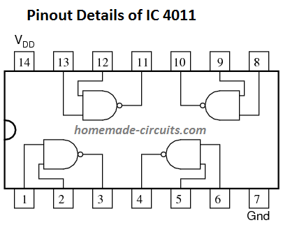
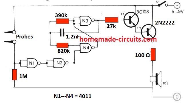 This also means that the circuit will not be able to detect distilled or deionised water.
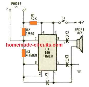 A tiny, cup full indicator circuit could be also created using the IC 555, as shown in the above diagram.
The IC 555 is rigged as an astable multivibrator.
As long as the probes are not touching the liquid inside the cup, the astable generates a low frequency 15 Hz clicking sound on the speaker.
When the cup is full, and the probes come in contact with the liquid, the frequency of the astable suddenly increases to 500 Hz sharp tone, which alerts the user regarding the cup full condition.
The speaker could be replaced with the piezo buzzer transducer also, to make the design very compact.
A tiny, cup full indicator circuit could be also created using the IC 555, as shown in the above diagram.
The IC 555 is rigged as an astable multivibrator.
As long as the probes are not touching the liquid inside the cup, the astable generates a low frequency 15 Hz clicking sound on the speaker.
When the cup is full, and the probes come in contact with the liquid, the frequency of the astable suddenly increases to 500 Hz sharp tone, which alerts the user regarding the cup full condition.
The speaker could be replaced with the piezo buzzer transducer also, to make the design very compact.

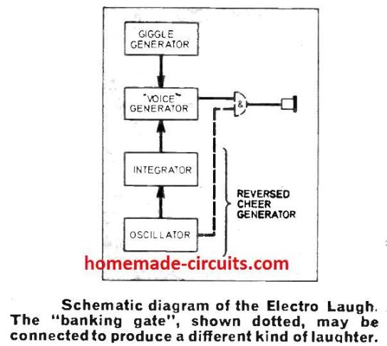 Due to the fact that, there's no "particular laughing sound" that may be followed in our electronic imitation circuit, hence the decision had to be an overall replica of most commonly heard laughter types.
Upon investigation, it was found that the majority of laughter sound felt like beginning at a specific stage within the sound range, which drops pretty fast to a frequency level approximately an octave lower.
It can be compared to a soccer cheering heard in the reverse tone.
This sort of noise identified as a glissando) may be easily generated through the output voltage that comes from a basic integrator powered by a low frequency square wave oscillator which alters the voice generator frequency.
Also, the circuit must have the ability to make and break this characteristic in quite short bursts.
Each of these burst is supposed to cause a kind of warbling impact on the existing frequency with a declining frequency.
To accomplish this an extra oscillator, named as the "giggle generator" has been included.
This stage continuously toggles the frequency of the basic "voice generator" from a single set position within the voice range to a new one.
Once powered, the voltage from the integrator part of the "reversed cheer" generator is going to increase and decrease, creating a proportionate increase and decrease in the amplitude of the tone of voice.
However in case desired, the rising section of the tone may be prevented through a blanking gate network, as indicated in the above schematic block diagram.
Due to the fact that, there's no "particular laughing sound" that may be followed in our electronic imitation circuit, hence the decision had to be an overall replica of most commonly heard laughter types.
Upon investigation, it was found that the majority of laughter sound felt like beginning at a specific stage within the sound range, which drops pretty fast to a frequency level approximately an octave lower.
It can be compared to a soccer cheering heard in the reverse tone.
This sort of noise identified as a glissando) may be easily generated through the output voltage that comes from a basic integrator powered by a low frequency square wave oscillator which alters the voice generator frequency.
Also, the circuit must have the ability to make and break this characteristic in quite short bursts.
Each of these burst is supposed to cause a kind of warbling impact on the existing frequency with a declining frequency.
To accomplish this an extra oscillator, named as the "giggle generator" has been included.
This stage continuously toggles the frequency of the basic "voice generator" from a single set position within the voice range to a new one.
Once powered, the voltage from the integrator part of the "reversed cheer" generator is going to increase and decrease, creating a proportionate increase and decrease in the amplitude of the tone of voice.
However in case desired, the rising section of the tone may be prevented through a blanking gate network, as indicated in the above schematic block diagram.
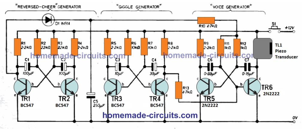
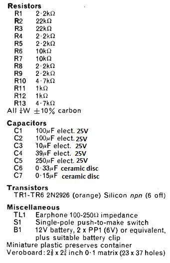 Please refer to the oscillator section in the "reversed cheer" generator stage of the above figure.
As soon as power is switched ON, we could imagine TR1 switching ON and causing C1 junction at TR1 collector to be pulled at almost ground level.
Because of this, C1 that may have by now charged to nearly + supply potential, starts to discharge.
During this period C2 swiftly charges up to the supply potential.
When C1 has discharged to around 0.6V (i.e., the Vbe of TR2) TR2 begin to turn ON.
Because of the feedback between the two sides of the circuit, a fast changeover takes place causing TR2 to turn ON intensely and TR1 to switch OFF.
This operation then goes on and on repeatedly with C2 discharging and C1 charging, until the time TR1 activates again and TR2 gets deactivated.
This carries on infinitely, or until the circuit is powered off.
The C1, C2 discharge rates are primarily established with the values of R2 and R3, while the average time constant (1.4CR) decides the operating frequency.
The charging intervals for C1 and C2 are dependent around the values of R1 and R4, that normally tend to be quite small and therefore may be simply ignored.
During the time when TR1 is cut off, the positive potential from its collector is allowed to freely charge the capacitor C5. This causes the voltage across C5 to rise towards the supply level while TR1 continues to be in the non-conducting state.
However, when TR1 gets the opportunity to turn ON, it causes D1 to get reverse-biased.
Due to this C5 slowly discharges via R10, R11, R12, and the bases of TR5 and TR6.
This process in which C5 is charged and a discharged slowly, results in a constant variation of the voltage levels where C6 and C7 start discharging in the voice generator stage.
This impacts the average time constant of the frequency and consequently the output signal results also get affected.
This implies that the increase in the charging voltage across C5 does not cause a rising effect on the pitch of the signal.
The purpose of the "giggle generator" output is to momentarily force a quick switching of frequency of the "voice generator" while the "reversed cheer" is in action.
This is successfully implemented by linking the collector of TR4, to the base of TR6 through R13.
Please refer to the oscillator section in the "reversed cheer" generator stage of the above figure.
As soon as power is switched ON, we could imagine TR1 switching ON and causing C1 junction at TR1 collector to be pulled at almost ground level.
Because of this, C1 that may have by now charged to nearly + supply potential, starts to discharge.
During this period C2 swiftly charges up to the supply potential.
When C1 has discharged to around 0.6V (i.e., the Vbe of TR2) TR2 begin to turn ON.
Because of the feedback between the two sides of the circuit, a fast changeover takes place causing TR2 to turn ON intensely and TR1 to switch OFF.
This operation then goes on and on repeatedly with C2 discharging and C1 charging, until the time TR1 activates again and TR2 gets deactivated.
This carries on infinitely, or until the circuit is powered off.
The C1, C2 discharge rates are primarily established with the values of R2 and R3, while the average time constant (1.4CR) decides the operating frequency.
The charging intervals for C1 and C2 are dependent around the values of R1 and R4, that normally tend to be quite small and therefore may be simply ignored.
During the time when TR1 is cut off, the positive potential from its collector is allowed to freely charge the capacitor C5. This causes the voltage across C5 to rise towards the supply level while TR1 continues to be in the non-conducting state.
However, when TR1 gets the opportunity to turn ON, it causes D1 to get reverse-biased.
Due to this C5 slowly discharges via R10, R11, R12, and the bases of TR5 and TR6.
This process in which C5 is charged and a discharged slowly, results in a constant variation of the voltage levels where C6 and C7 start discharging in the voice generator stage.
This impacts the average time constant of the frequency and consequently the output signal results also get affected.
This implies that the increase in the charging voltage across C5 does not cause a rising effect on the pitch of the signal.
The purpose of the "giggle generator" output is to momentarily force a quick switching of frequency of the "voice generator" while the "reversed cheer" is in action.
This is successfully implemented by linking the collector of TR4, to the base of TR6 through R13.
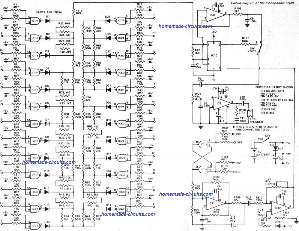
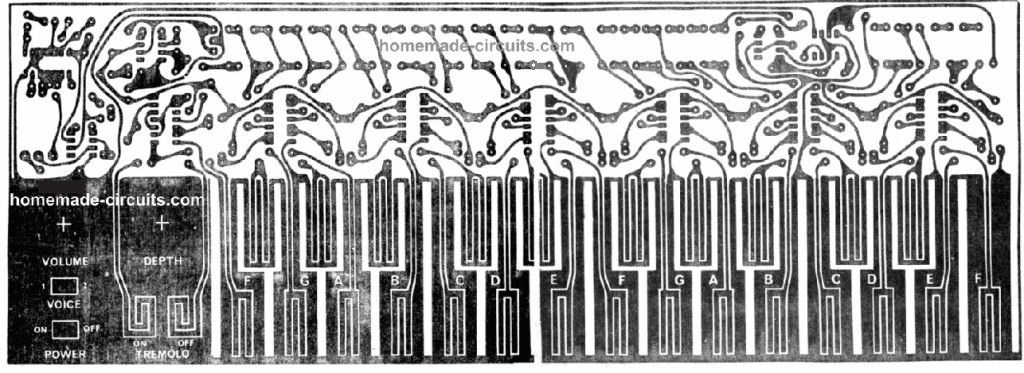

 Fig.3
Fig.3
 The (measured) characteristic of the woofer installed on a board that of the correction network and that of the adjusted loudspeaker are displayed in Fig.
1.
The (measured) characteristic of the woofer installed on a board that of the correction network and that of the adjusted loudspeaker are displayed in Fig.
1.
 Fig.1
To maintain the efficiency and power handling within tolerable limits the correction has been constrained to just above 1 octave.
The efficiency is decreased by 8 dB.
The use of a pair of woofers does not actually improve the efficiency (the overall impedance is lower although the dissipation is larger).
and the power output continues to be practically identical as that of one 210 mm woofer in closed box.
The tested characteristic are presented in Fig.
2.
Fig.1
To maintain the efficiency and power handling within tolerable limits the correction has been constrained to just above 1 octave.
The efficiency is decreased by 8 dB.
The use of a pair of woofers does not actually improve the efficiency (the overall impedance is lower although the dissipation is larger).
and the power output continues to be practically identical as that of one 210 mm woofer in closed box.
The tested characteristic are presented in Fig.
2.
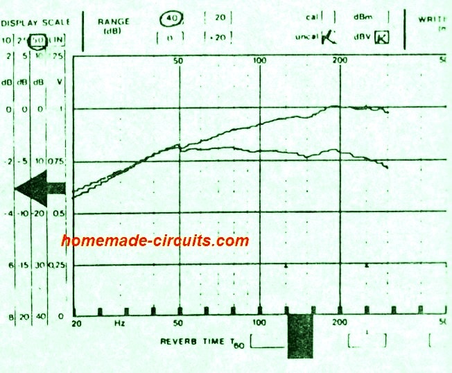 Fig.2
It is observed that the -3 dB cut-off frequency is reduced to about 35 Hz which is a good value for hi-Fi applications.
Note that the corrected curve consists of the effects of the low pass filter in order that it begins to slide of yet again over 200 Hz.
The resulting dc symbol is a narrow baffle that offers better bass output at lower Hz than several ˇ®traditional' speaker boxes.
It may seem as though the proposed open baffle layout will not reproduce the low frequencies nicely.
However that may be due to the fact that box designers usually do not enable for the effect of the real room or space, resulting in a low frequency peak as soon as the loudspeaker is utilized for the room.
The characteristics of the woofers tested in front and back are essentially the same at low frequencies.
This is simply not the situation with squawkers (mid-range units and tweeters, which implies that these need to be replicated at the rear end.
Moreover squakers have greatly curved frequency characteristics and inferior radiation efficiency.
For that reason it became important to put those units in a small housing
Fig.2
It is observed that the -3 dB cut-off frequency is reduced to about 35 Hz which is a good value for hi-Fi applications.
Note that the corrected curve consists of the effects of the low pass filter in order that it begins to slide of yet again over 200 Hz.
The resulting dc symbol is a narrow baffle that offers better bass output at lower Hz than several ˇ®traditional' speaker boxes.
It may seem as though the proposed open baffle layout will not reproduce the low frequencies nicely.
However that may be due to the fact that box designers usually do not enable for the effect of the real room or space, resulting in a low frequency peak as soon as the loudspeaker is utilized for the room.
The characteristics of the woofers tested in front and back are essentially the same at low frequencies.
This is simply not the situation with squawkers (mid-range units and tweeters, which implies that these need to be replicated at the rear end.
Moreover squakers have greatly curved frequency characteristics and inferior radiation efficiency.
For that reason it became important to put those units in a small housing
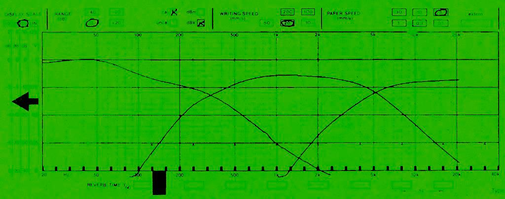 Fig.4
Filtering proper is done by L1-C1. This section gives a second-order slope approximately above 400 Hz (it looks to be fairly reduced Fig.
4, but that may be since the curves there relate to the electrical output only: the efficiencies of the drive units are not included.
Resistor R1 guarantees a fairly steady resistance at the output of the system, regardless of the impact of L2-R2 and the frequency-dependent impedance of the woofers.
The portion for the squawkers comprises of L4-C2 for the roll-off at 400 Hz and L5-C3 for the same at 5 kHz.
The slopes are approximately 12 dB per octave.
Along with the natural roll-off of the tweeters, this produces a sharper slope, which is crucial to make sure that the mid-range devices do not deal with an excessive amount of power.
Attenuator R3-R4 between the section and the drive units offers level matching at near 3.5 dB.
The tweeter section (second-order) includes L5-C4.
Attenuator R5-R6 provides level matching approximately at 5.5 dB to offer an ultimate, at acoustic frequency response.
The cross-over network is best developed over a small general purpose veroboard see Fig.
5 for an appropriate component layout.
Fig.4
Filtering proper is done by L1-C1. This section gives a second-order slope approximately above 400 Hz (it looks to be fairly reduced Fig.
4, but that may be since the curves there relate to the electrical output only: the efficiencies of the drive units are not included.
Resistor R1 guarantees a fairly steady resistance at the output of the system, regardless of the impact of L2-R2 and the frequency-dependent impedance of the woofers.
The portion for the squawkers comprises of L4-C2 for the roll-off at 400 Hz and L5-C3 for the same at 5 kHz.
The slopes are approximately 12 dB per octave.
Along with the natural roll-off of the tweeters, this produces a sharper slope, which is crucial to make sure that the mid-range devices do not deal with an excessive amount of power.
Attenuator R3-R4 between the section and the drive units offers level matching at near 3.5 dB.
The tweeter section (second-order) includes L5-C4.
Attenuator R5-R6 provides level matching approximately at 5.5 dB to offer an ultimate, at acoustic frequency response.
The cross-over network is best developed over a small general purpose veroboard see Fig.
5 for an appropriate component layout.
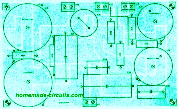 Fig.5
The cored inductors are pretty heavy and, therefore must be clamped properly, if possible with nonmetallic nuts, bolts and washers.
Inductors L1, L2, and L4 are bobbin types with an HQ core.
This material does not create distortion at both high and low frequencies and is also quite cheap.
Since L1 and L2 are supposed to carry relatively substantial currents are air core inductors or have a nonferrous or inferior core material.
Despite the fact that C2 is chosen as a bipolar electrolytic, an MKT type can also be used as effectively.
Fig.5
The cored inductors are pretty heavy and, therefore must be clamped properly, if possible with nonmetallic nuts, bolts and washers.
Inductors L1, L2, and L4 are bobbin types with an HQ core.
This material does not create distortion at both high and low frequencies and is also quite cheap.
Since L1 and L2 are supposed to carry relatively substantial currents are air core inductors or have a nonferrous or inferior core material.
Despite the fact that C2 is chosen as a bipolar electrolytic, an MKT type can also be used as effectively.

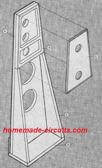 A sideview of the design thus far appears like an individual, 50 mm [2 in) solid section that broadens on the base.
Finish off this as necessary in lacquer or veneer.
Remember the panel E Once the laquer or veneer dries up, work the cords for the loudspeakers and install the drive units at the frontˇŞdon't overlook the cables for the back squawker and tweeter.
Hook up the cables to the devices.
Tag the cable ends, in order that it doesn't create confusions afterwards regarding the various cable terminals.
The holes through which by which the wires go through should be sealed waterproof using, e.
g.
a glue gun.
Subsequently, secure panel E with chipboard screws towards the top rear as indicated in Fig.
6b.
The screw heads should be counter-sunk.
A sideview of the design thus far appears like an individual, 50 mm [2 in) solid section that broadens on the base.
Finish off this as necessary in lacquer or veneer.
Remember the panel E Once the laquer or veneer dries up, work the cords for the loudspeakers and install the drive units at the frontˇŞdon't overlook the cables for the back squawker and tweeter.
Hook up the cables to the devices.
Tag the cable ends, in order that it doesn't create confusions afterwards regarding the various cable terminals.
The holes through which by which the wires go through should be sealed waterproof using, e.
g.
a glue gun.
Subsequently, secure panel E with chipboard screws towards the top rear as indicated in Fig.
6b.
The screw heads should be counter-sunk.
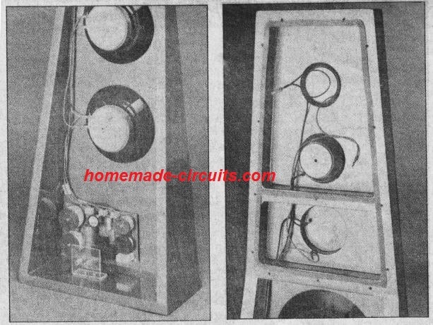 Fig.7
Cover up the spaces between the panels with appropriate taping.
After that install the rear squawker and tweeter.
Ensure that the cable connections to these sections are replication of those in front; meaning, connect the + line of the front tweeter to the - line of the rear tweeter, and likewise with the mid-range units.
The electrical polarity in accordance with the cross-over network will depend on the front loudspeakers.
Next, install the cross-over system under the woofers as demonstrated in the photograph in Fig.
7. Lastly, create an L-shaped mount as presented in Fig.
7, bolt this to the base panel as indicated and fit the sockets to this.
Hook up the sockets to the cross-over network as suitable.
Fig.7
Cover up the spaces between the panels with appropriate taping.
After that install the rear squawker and tweeter.
Ensure that the cable connections to these sections are replication of those in front; meaning, connect the + line of the front tweeter to the - line of the rear tweeter, and likewise with the mid-range units.
The electrical polarity in accordance with the cross-over network will depend on the front loudspeakers.
Next, install the cross-over system under the woofers as demonstrated in the photograph in Fig.
7. Lastly, create an L-shaped mount as presented in Fig.
7, bolt this to the base panel as indicated and fit the sockets to this.
Hook up the sockets to the cross-over network as suitable.
 The circuit utilizes a discarded 60 watt loudspeaker for producing the banging loud pistol sound.
The main components that form the power oscillator circuit are T1 and T2 along with the mains transformer TR1.
S1 is used to initiate or power up the above circuit stage momentarily with a single push of the button.
The zener diodes provide the required protection to the transistors against inductive voltage spikes.
Since the oscillator circuit is a self oscillating circuit, its frequency is determined by the core material of the transformer, and also the magnitude of current drawn from the secondary of the transformer.
The circuit utilizes a discarded 60 watt loudspeaker for producing the banging loud pistol sound.
The main components that form the power oscillator circuit are T1 and T2 along with the mains transformer TR1.
S1 is used to initiate or power up the above circuit stage momentarily with a single push of the button.
The zener diodes provide the required protection to the transistors against inductive voltage spikes.
Since the oscillator circuit is a self oscillating circuit, its frequency is determined by the core material of the transformer, and also the magnitude of current drawn from the secondary of the transformer.
 This stereo mixer circuit is additionally simple to customize.
For instance, We replaced low-noise amplifiers for the 741's, and employed 1% metal - film resistors.
We furthermore made use of slide potentiometers for the faders and line -level controls.
We modified the quantity of in puts also.
Rather than just a couple of MIC inputs and a single line input, We expected to get a total of 8 MIC inputs and 4 LINE inputs.
This stereo mixer circuit is additionally simple to customize.
For instance, We replaced low-noise amplifiers for the 741's, and employed 1% metal - film resistors.
We furthermore made use of slide potentiometers for the faders and line -level controls.
We modified the quantity of in puts also.
Rather than just a couple of MIC inputs and a single line input, We expected to get a total of 8 MIC inputs and 4 LINE inputs.
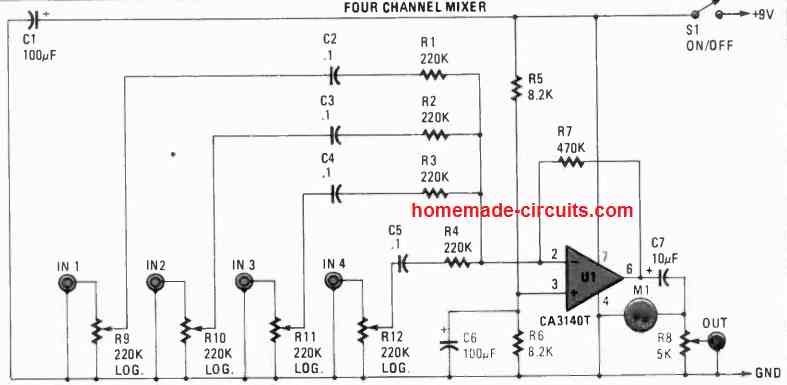 The next image shows a 4 channel mixer, in which 4 different audio signals can be fed to the indicated relevant inputs IN1----IN4 ports, the opamp will mix them all to produce a common mixed output at the port indicated as OUT.
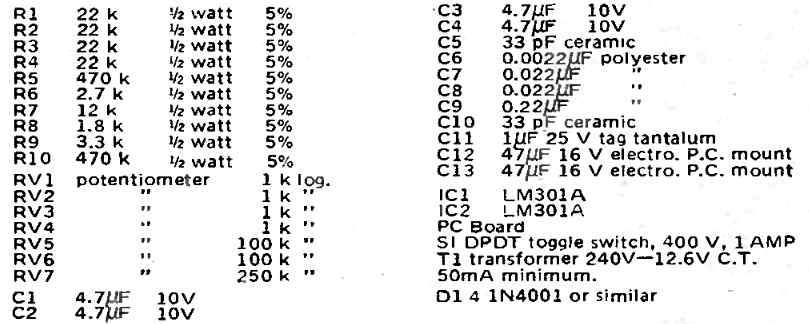 The signal supplied by means of a sensor involving audio frequencies, for example a microphone, a guitar-string sensor, etc all require a signal boosting before the output can be used to drive a main amplifier.
The 4 channel preamplifier displayed above can work with signals as low as 2 mV levels, comes with an input impedance of 1 k, offers a gain of around 1600, and provides an output swing as high as 3.2 V for 2 mV input.
It exhibits relatively small distortion and is built to accept four external inputs, all featuring their own level control.
An exclusive tone control system is integrated that allows bass and treble signal frequencies to be adjusted through a range of ˇŔ10 dB (at 100 Hz and 10 kHz respectively).
Even though largely designed for mixing audio signals in leisure purposes, the circuit could also be applied as a single-input, adjustable -gain unit in just about any application where gain and frequency modification are essential.
The signal supplied by means of a sensor involving audio frequencies, for example a microphone, a guitar-string sensor, etc all require a signal boosting before the output can be used to drive a main amplifier.
The 4 channel preamplifier displayed above can work with signals as low as 2 mV levels, comes with an input impedance of 1 k, offers a gain of around 1600, and provides an output swing as high as 3.2 V for 2 mV input.
It exhibits relatively small distortion and is built to accept four external inputs, all featuring their own level control.
An exclusive tone control system is integrated that allows bass and treble signal frequencies to be adjusted through a range of ˇŔ10 dB (at 100 Hz and 10 kHz respectively).
Even though largely designed for mixing audio signals in leisure purposes, the circuit could also be applied as a single-input, adjustable -gain unit in just about any application where gain and frequency modification are essential.

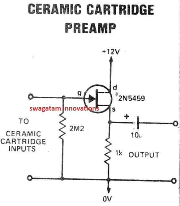 When using the stages outlined above practically any audio options could be mixed or blended by the user to get a stereo transmission specifically suited for driving power amplifiers straight away.
The mixed signals may also obviously be applied to feed headphones etc.
The inputs from CD players, microphones, Ipods, cellphones etc should be appropriately matched up to the inputs of the mixer board.
To get this done the proper preamplifiers needs to be determined and built.
Even so, the audio mixing range could be practically endless.
Before you start building consider which preamplifiers you might need, consider which kind of sockets you would like to work with, and the number of channels you would like (although demonstrated as 4 channel, the mixer could be extended with the addition of further control pots and mixer resistors).
When using the stages outlined above practically any audio options could be mixed or blended by the user to get a stereo transmission specifically suited for driving power amplifiers straight away.
The mixed signals may also obviously be applied to feed headphones etc.
The inputs from CD players, microphones, Ipods, cellphones etc should be appropriately matched up to the inputs of the mixer board.
To get this done the proper preamplifiers needs to be determined and built.
Even so, the audio mixing range could be practically endless.
Before you start building consider which preamplifiers you might need, consider which kind of sockets you would like to work with, and the number of channels you would like (although demonstrated as 4 channel, the mixer could be extended with the addition of further control pots and mixer resistors).
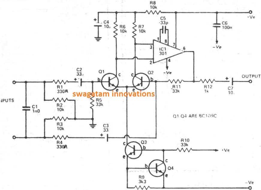 Over this figure R2 + R3 need to be incorporated in the computation.
Even though we all posses just one input, the output from this circuit makes it possible to griddle the output through stereo by utilizing a couple of 10k resistors or a 20k linear pot using the wiper attached to the output enables you to pan the output via left to right.
In case a balanced MIC is applied R2 values will be as follows microphone R2 = 4k7 (limiting R2 47k) if employed with balanced preamp as input to restrict R2 = 15k
Over this figure R2 + R3 need to be incorporated in the computation.
Even though we all posses just one input, the output from this circuit makes it possible to griddle the output through stereo by utilizing a couple of 10k resistors or a 20k linear pot using the wiper attached to the output enables you to pan the output via left to right.
In case a balanced MIC is applied R2 values will be as follows microphone R2 = 4k7 (limiting R2 47k) if employed with balanced preamp as input to restrict R2 = 15k


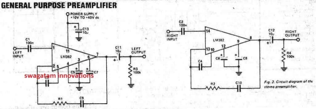
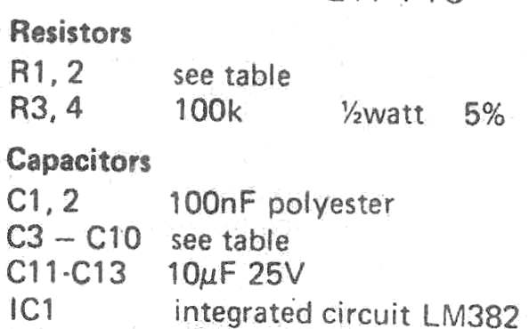
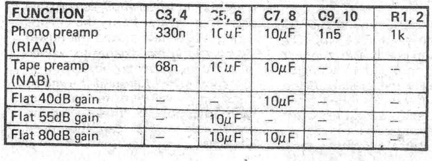
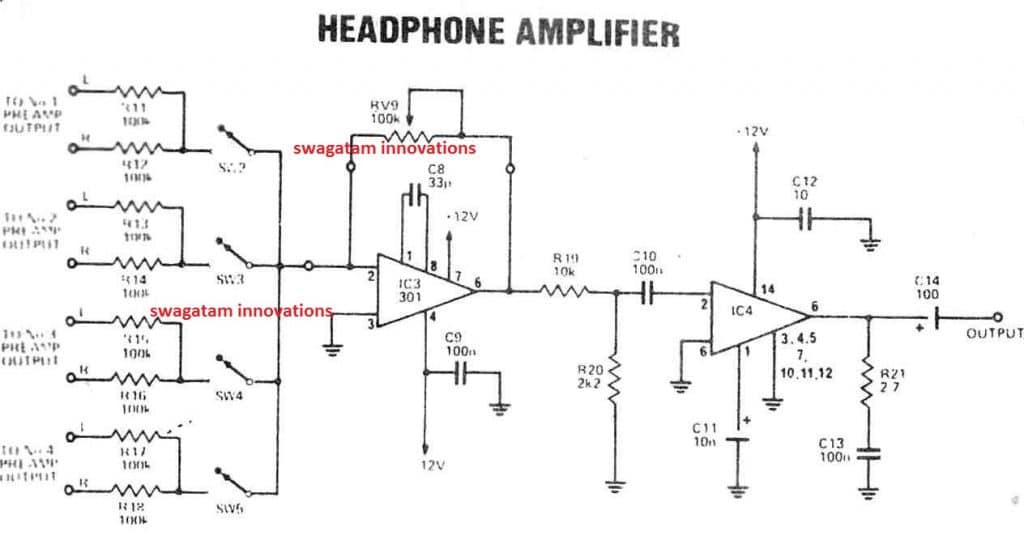
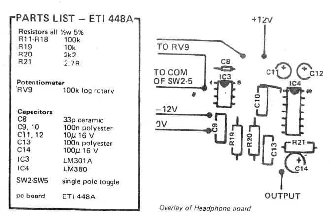 This is primarily to safeguard your ears and decrease the power dissipation of the LM 380 or else a little heatsink could be needed.
The volume control could be attached to the trunk of the mixer since it is not necessarily tweaked frequently.
This is primarily to safeguard your ears and decrease the power dissipation of the LM 380 or else a little heatsink could be needed.
The volume control could be attached to the trunk of the mixer since it is not necessarily tweaked frequently.


 Figure 1
According to Figure 1, Hafler designed the circuit to enable the rear speakers generate the difference of signal between right and left output.
While every stereo encoded system maintains difference of signal between the right and left channel, it is that difference of signal when received by the rear speakers gets reproduced.
However, it is vital to keep in mind not to earth the negative terminals of the rear speakers, else the rear will behave parallel to the main front speakers.
Figure 1
According to Figure 1, Hafler designed the circuit to enable the rear speakers generate the difference of signal between right and left output.
While every stereo encoded system maintains difference of signal between the right and left channel, it is that difference of signal when received by the rear speakers gets reproduced.
However, it is vital to keep in mind not to earth the negative terminals of the rear speakers, else the rear will behave parallel to the main front speakers.
 Figure 2
As an alternative we have tried using a 600ohm unit.
But it is for the impedance the output we received was not good as it lacks bass.
However, upon loading the transformer, it increased the bass quality but the preamp doesnˇŻt seem to work at its fullest because of the impedance.
It is for this reason that we have used telephonic transformers with 600:600ohms, and it worked well.
The circuit in Figure 2 illustrates the way we followed.
Following this design, it worked, but it has very low impedance on all cases barring solid-state preamp.
Using 600ohm unit, the loss generated is around 3dB.
The low frequency is -3dB on 100Hz.
However, it varies based upon the quality of the transformer.
600ohm telephony transformer is widely available in the market, but many of them are not up to the mark to use it in this experiment.
Most of the hi-powered transformers are sold in bulk and is therefore hard to procure a single copy.
So, the alternative would be to use dual opamp to design the system, and its process is mentioned below in detail.
Figure 2
As an alternative we have tried using a 600ohm unit.
But it is for the impedance the output we received was not good as it lacks bass.
However, upon loading the transformer, it increased the bass quality but the preamp doesnˇŻt seem to work at its fullest because of the impedance.
It is for this reason that we have used telephonic transformers with 600:600ohms, and it worked well.
The circuit in Figure 2 illustrates the way we followed.
Following this design, it worked, but it has very low impedance on all cases barring solid-state preamp.
Using 600ohm unit, the loss generated is around 3dB.
The low frequency is -3dB on 100Hz.
However, it varies based upon the quality of the transformer.
600ohm telephony transformer is widely available in the market, but many of them are not up to the mark to use it in this experiment.
Most of the hi-powered transformers are sold in bulk and is therefore hard to procure a single copy.
So, the alternative would be to use dual opamp to design the system, and its process is mentioned below in detail.
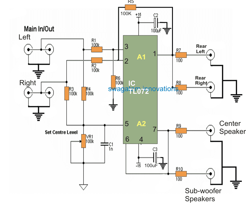 Figure 3
While the new design [Figure 3] will follow HaflerˇŻs principle, this new circuit has simplified wiring, albeit we needed extra power amps.
There is now a center channel signal and the sub-woofer to receive mono signal is also set.
You may have encountered similar type of circuit on other papers, but there are some twists into it.
We avoided any active electronics on left/right channels and introduced opamps to zero down the factor that may cause degradation of sound.
The 50K impedance will not pose any barrier for a preamp, as the main signal is parallel to the additional circuit.
Extra volume control has been excluded from the system, because of the presence of volume control in the preamp.
Moreover, the power amp of rear channel also has level control to balance the front and rear levels.
Please note, if you are following the circuit as in Figure 3 do ensure to make the rear speakers wired-out phase.
Let one speaker connect to the amp on a normal fashion and the second should be connected keeping the leads of speaker reversed.
Though the difference maybe negligible, but to derive the best quality effect it is always advisable to opt for out-of-phase connection.
This helps in maintaining left-right and right-left signals.
Figure 3
While the new design [Figure 3] will follow HaflerˇŻs principle, this new circuit has simplified wiring, albeit we needed extra power amps.
There is now a center channel signal and the sub-woofer to receive mono signal is also set.
You may have encountered similar type of circuit on other papers, but there are some twists into it.
We avoided any active electronics on left/right channels and introduced opamps to zero down the factor that may cause degradation of sound.
The 50K impedance will not pose any barrier for a preamp, as the main signal is parallel to the additional circuit.
Extra volume control has been excluded from the system, because of the presence of volume control in the preamp.
Moreover, the power amp of rear channel also has level control to balance the front and rear levels.
Please note, if you are following the circuit as in Figure 3 do ensure to make the rear speakers wired-out phase.
Let one speaker connect to the amp on a normal fashion and the second should be connected keeping the leads of speaker reversed.
Though the difference maybe negligible, but to derive the best quality effect it is always advisable to opt for out-of-phase connection.
This helps in maintaining left-right and right-left signals.
 The full duplex communicator design:
A full duplex communication is a two way communication, in which both the parties are able to communicate simultaneously.
To keep the design as simple as possible we use a standard FM radio as the receiver and a simple FM transmitter.
We need two FM radios and two transmitters to establish full duplex communication.
In between two communication sets the repeater will be placed to extend the signal.
A good example for full duplex communication is telecommunication and the proposed design works similarly.
The SET ˇ®AˇŻs FM receiver is tuned to SET ˇ®BˇŻs transmitter and SET ˇ®BˇŻs FM receiver is tuned to SET ˇ®AˇŻs transmitter.
Thus we can achieve simultaneous communication between them.
The given transmitter design can transmit up to 200 meter on best case scenario.
Adjust the trim capacitor for tuning the transmitter.
The full duplex communicator design:
A full duplex communication is a two way communication, in which both the parties are able to communicate simultaneously.
To keep the design as simple as possible we use a standard FM radio as the receiver and a simple FM transmitter.
We need two FM radios and two transmitters to establish full duplex communication.
In between two communication sets the repeater will be placed to extend the signal.
A good example for full duplex communication is telecommunication and the proposed design works similarly.
The SET ˇ®AˇŻs FM receiver is tuned to SET ˇ®BˇŻs transmitter and SET ˇ®BˇŻs FM receiver is tuned to SET ˇ®AˇŻs transmitter.
Thus we can achieve simultaneous communication between them.
The given transmitter design can transmit up to 200 meter on best case scenario.
Adjust the trim capacitor for tuning the transmitter.
 Full duplex communication: (without repeater)
 When the repeater comes in between the transmission and reception, the whole system gets slightly complicated.
LetˇŻs assume some factors and simulate the situation:
ˇ¤ Let, SET ˇ®AˇŻs transmission frequency be 90MHz.
Then the receiving frequency at repeater must be 90MHz (RX1).
Let the repeating frequency at TX1 be 92MHz.
Then the receiving frequency at SET ˇ®BˇŻ must be 92MHz.
similarly for another channel.
ˇ¤ All the frequencies used in repeater must not be used more than once.
For example: 90MHz at TX1 and this frequency should not be used anywhere in the repeater circuit.
ˇ¤ The transmission frequency, repeating frequency and receiving frequency must be well determined before communication just to avoid confusion.
NOTE: Here the node represents one set of transmitter and receiver.
Distance between node and repeater is 150 meter is an assumption; it could be greater or less depending on environment and antenna length.
Use a radio with good sensitivity for this project.
When the repeater comes in between the transmission and reception, the whole system gets slightly complicated.
LetˇŻs assume some factors and simulate the situation:
ˇ¤ Let, SET ˇ®AˇŻs transmission frequency be 90MHz.
Then the receiving frequency at repeater must be 90MHz (RX1).
Let the repeating frequency at TX1 be 92MHz.
Then the receiving frequency at SET ˇ®BˇŻ must be 92MHz.
similarly for another channel.
ˇ¤ All the frequencies used in repeater must not be used more than once.
For example: 90MHz at TX1 and this frequency should not be used anywhere in the repeater circuit.
ˇ¤ The transmission frequency, repeating frequency and receiving frequency must be well determined before communication just to avoid confusion.
NOTE: Here the node represents one set of transmitter and receiver.
Distance between node and repeater is 150 meter is an assumption; it could be greater or less depending on environment and antenna length.
Use a radio with good sensitivity for this project.
 NOTE: Adjust the volume knob optimally so that the right amount of volume goes to the transmitter.
DonˇŻt ramp-up the volume to maximum, otherwise there could be a good chance of distortion in re-transmission.
NOTE: Adjust the volume knob optimally so that the right amount of volume goes to the transmitter.
DonˇŻt ramp-up the volume to maximum, otherwise there could be a good chance of distortion in re-transmission.
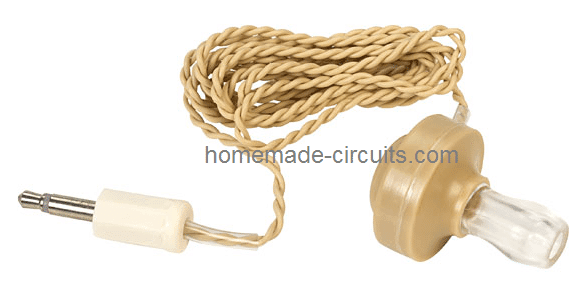 A crystal earphone is recommended here, due to its high impedance property, which makes it a voltage sensitive device rather than a current sensitive device.
Meaning the earphone would be able to transform even the weakest of voltage frequencies regardless of the current (mA) magnitude, enabling hearing of even the feeblest of the radio signals.
This is crucial since no external power is being used for the amplification.
Typically a crystal earphone with a range of 2K ohms should be just good enough value for our crystal radio application.
To check the efficiency level of a crystal earphone, you could probably do a few simple but very interesting tests with it.
The first test could be performed by simply scratching the end terminals of its wires with each other, this should produce faint clicking sound in the earphone, another test can be tried by firmly holding the stripped ends of its wires and standing near your home mains line....this should enable you to hear a reasonably strong humming sound in the earphone.
These tests might be enough to convince you regarding the high level of sensitivity that these units may be specified with.
This high sensitivity of the crystal earphone along with the resonant tuning of the radio's LC tank circuit stage, together ensures a sound level that's loud enough to be clearly heard without using any form of external power supply.
With no external power, the weak electrical pulses of the radio signal is itself processed and used by the crystal circuit and the crystal earphone and is made efficiently audible in our ears.
This radio can be used for hearing local stations at around 50kms range during daytime and from over 100 of miles away at night when the surrounding noise is much reduced compared to the daytime commotion.
The key element that helps the crystal set to grab even the minutest of radio reception is the length of the antenna used, it should be preferably a 30to 40 meter long flexible wire suitably tied and hung at some elevation such as a tree branch etc.
The antenna will be capable of capturing quite many radio stations including the night time DX stations, due to the favorable ionosphere transition after the sun goes down.
The second crucial element of the design is the "earthing" or the ground quality, which should not be ignored otherwise the radio could simply refuse to provide the intended results.
A crystal earphone is recommended here, due to its high impedance property, which makes it a voltage sensitive device rather than a current sensitive device.
Meaning the earphone would be able to transform even the weakest of voltage frequencies regardless of the current (mA) magnitude, enabling hearing of even the feeblest of the radio signals.
This is crucial since no external power is being used for the amplification.
Typically a crystal earphone with a range of 2K ohms should be just good enough value for our crystal radio application.
To check the efficiency level of a crystal earphone, you could probably do a few simple but very interesting tests with it.
The first test could be performed by simply scratching the end terminals of its wires with each other, this should produce faint clicking sound in the earphone, another test can be tried by firmly holding the stripped ends of its wires and standing near your home mains line....this should enable you to hear a reasonably strong humming sound in the earphone.
These tests might be enough to convince you regarding the high level of sensitivity that these units may be specified with.
This high sensitivity of the crystal earphone along with the resonant tuning of the radio's LC tank circuit stage, together ensures a sound level that's loud enough to be clearly heard without using any form of external power supply.
With no external power, the weak electrical pulses of the radio signal is itself processed and used by the crystal circuit and the crystal earphone and is made efficiently audible in our ears.
This radio can be used for hearing local stations at around 50kms range during daytime and from over 100 of miles away at night when the surrounding noise is much reduced compared to the daytime commotion.
The key element that helps the crystal set to grab even the minutest of radio reception is the length of the antenna used, it should be preferably a 30to 40 meter long flexible wire suitably tied and hung at some elevation such as a tree branch etc.
The antenna will be capable of capturing quite many radio stations including the night time DX stations, due to the favorable ionosphere transition after the sun goes down.
The second crucial element of the design is the "earthing" or the ground quality, which should not be ignored otherwise the radio could simply refuse to provide the intended results.
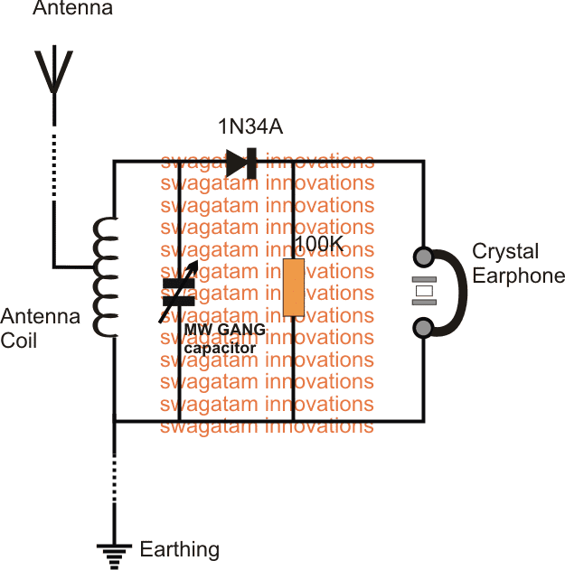
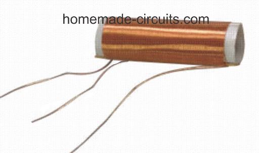
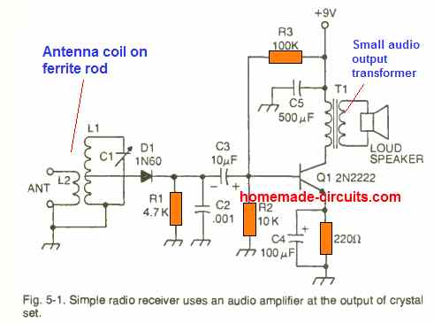 If you have any questions or doubts, don't hesitate to put it forth through comments below.
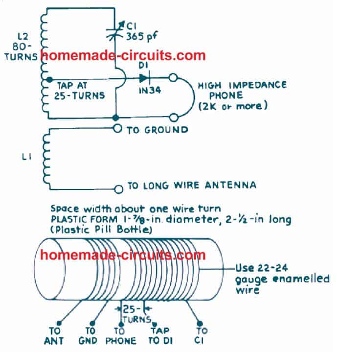
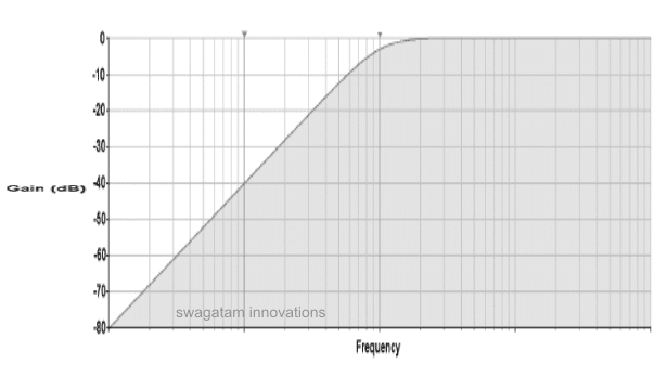 The following two images are configured as standard high-pass filter circuits, where the first one is designed to work with a dual supply whereas the second one is specified to operate with a single supply.
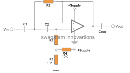 In both the above configurations, the opamp forms the central processing active component, while the associated resistors and capacitors wired across the input pins of the opamp are introduced for determining the high-pass filter cut-off point, depending upon how the values of these passive components are calculated as per the users specifications or requirements.
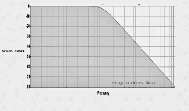 The following images depict the standard opamp based low pass filter circuits.
The first one needs to be powered by a dual supply, and the second one works using a single supply voltage.
The following images depict the standard opamp based low pass filter circuits.
The first one needs to be powered by a dual supply, and the second one works using a single supply voltage.
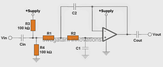
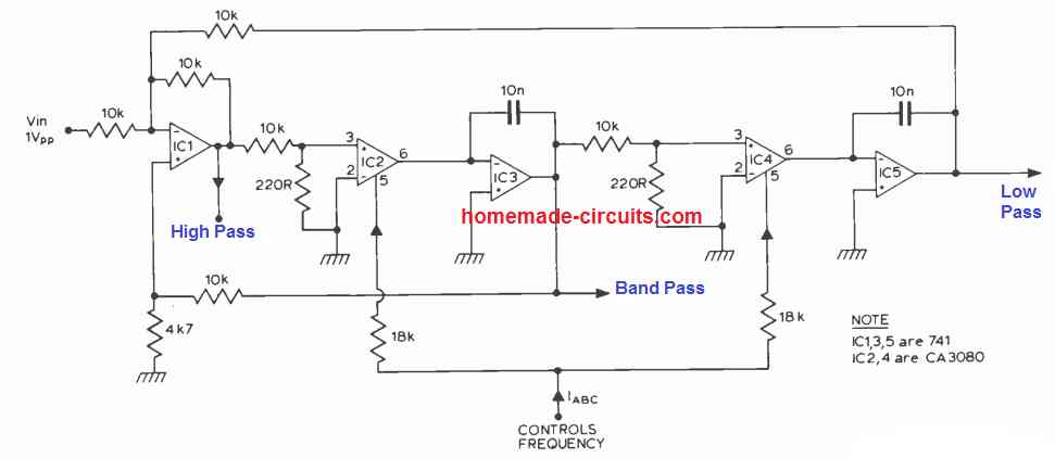 In the proposed filter design, this specific resonant frequency is linearly proportional to the gain of the two integrators.
A couple of CA3080's, (IC2, 4) are actually configured to supply the adjustable gain, the resonant frequency being held proportional to the current IABC.
Working with 741 op amps for IC3 it may be possible to get a control range of 100 to 1, (resonant frequency).
If the ICs CA3140's are applied in place of 741's then this range could be expanded to practically 10,000 to 1.
More Info:https://drive.google.com/file/d/1yo_WH0NzYg43ro_X0ZrXoLYSM5XOzKU8/view?usp=sharing
In the proposed filter design, this specific resonant frequency is linearly proportional to the gain of the two integrators.
A couple of CA3080's, (IC2, 4) are actually configured to supply the adjustable gain, the resonant frequency being held proportional to the current IABC.
Working with 741 op amps for IC3 it may be possible to get a control range of 100 to 1, (resonant frequency).
If the ICs CA3140's are applied in place of 741's then this range could be expanded to practically 10,000 to 1.
More Info:https://drive.google.com/file/d/1yo_WH0NzYg43ro_X0ZrXoLYSM5XOzKU8/view?usp=sharing
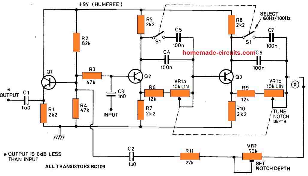
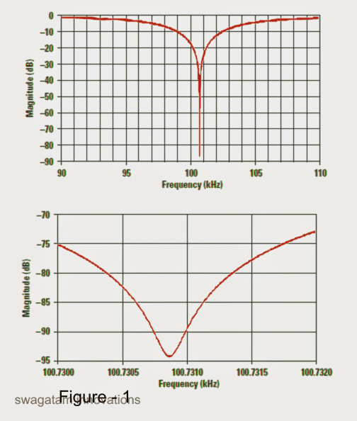 2) Therefore, it must be understood that the more significant factor to be improved is the center frequency and the Q, and the designer should focus on this instead of the depth of the notch.
The main objective while making a notch filter design should be the level of rejection of the unwanted interfering frequency, this must be optimal.
3) The above issue can be resolved optimally be preferring the best values for the R and the C components, which can be implemented by correctly using the RC calculator shown in Reference 1, which can be used for appropriately identifying the R0, and C0 for a particular notch filter designing application.
The following data will explore and help to understand the designing of some interetsing notch filter topologies:
2) Therefore, it must be understood that the more significant factor to be improved is the center frequency and the Q, and the designer should focus on this instead of the depth of the notch.
The main objective while making a notch filter design should be the level of rejection of the unwanted interfering frequency, this must be optimal.
3) The above issue can be resolved optimally be preferring the best values for the R and the C components, which can be implemented by correctly using the RC calculator shown in Reference 1, which can be used for appropriately identifying the R0, and C0 for a particular notch filter designing application.
The following data will explore and help to understand the designing of some interetsing notch filter topologies:
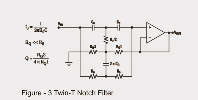 Although the above indicated notch filter circuit is reasonably efficient, it might have certain disadvantageous owing to the extreme simplicity that it bears, as given below:
The design makes use of 6 precision components for its tuning, wherein a couple of these for attaining ratios of the others.
If this complication requires to be avoided, the circuit might require the inclusion of 8 additional precision components, such as R0/2 = 2nos of R0 in parallel and 2 into C0 = 2 nos of C0 in parallel.
A Twin-T topology doesn't readily work with single power supplies, and does not comply with full-fledged differential amplifiers.
The range of resistor values keeps increasing due to the RQ < < R0 necessity which in turn may influence on the level of depth of the desired center frequency.
However, even with the above hassles, if the user succeeds in optimizing the design with high quality precise components, a reasonably effective filtration can be expected and implemented for the given application.
Although the above indicated notch filter circuit is reasonably efficient, it might have certain disadvantageous owing to the extreme simplicity that it bears, as given below:
The design makes use of 6 precision components for its tuning, wherein a couple of these for attaining ratios of the others.
If this complication requires to be avoided, the circuit might require the inclusion of 8 additional precision components, such as R0/2 = 2nos of R0 in parallel and 2 into C0 = 2 nos of C0 in parallel.
A Twin-T topology doesn't readily work with single power supplies, and does not comply with full-fledged differential amplifiers.
The range of resistor values keeps increasing due to the RQ < < R0 necessity which in turn may influence on the level of depth of the desired center frequency.
However, even with the above hassles, if the user succeeds in optimizing the design with high quality precise components, a reasonably effective filtration can be expected and implemented for the given application.
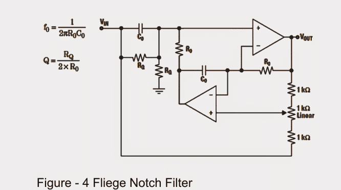 1) It incorporates just a couple of precision components in the form of Rs and Cs in order to fulfill an accurate center frequency tuning.
2) One appreciable aspect about this design is that it allows slight inaccuracies within the components and the settings without affecting the depth of the notch point, although the center frequency could change a bit accordingly.
3) You'll find a couple of resistors responsible for determining the center frequency discretely whose values may not be extremely critical
4) The configuration enables the setting up of the center frequency with a reasonably narrow range without influencing the notch depth to a significant level.
However, the negative thing about this toplogy is its use of two opamps, and yet still it does not become usable with differential amplifiers.
1) It incorporates just a couple of precision components in the form of Rs and Cs in order to fulfill an accurate center frequency tuning.
2) One appreciable aspect about this design is that it allows slight inaccuracies within the components and the settings without affecting the depth of the notch point, although the center frequency could change a bit accordingly.
3) You'll find a couple of resistors responsible for determining the center frequency discretely whose values may not be extremely critical
4) The configuration enables the setting up of the center frequency with a reasonably narrow range without influencing the notch depth to a significant level.
However, the negative thing about this toplogy is its use of two opamps, and yet still it does not become usable with differential amplifiers.
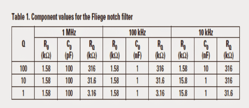 Table 1 demonstrates the component values which were put to use for the schematic in Figure 4. There seemed to be no sense in carrying out simulations at or above 10 MHz mainly because laboratory tests were essentially conducted as a start-up, and 1 MHz was the leading frequency where a notch filter was needed to be applied.
A word regarding capacitors: Despite the fact that the capacitance is merely a "number" for simulations, real capacitors are designed of unique dielectric elements.
For 10 kHz, resistor value stretch obligated the capacitor to a value of 10 nF.
Although this did the trick correctly in demo, it called for an adjustment from an NPO dielectric to an X7R dielectric in the lab which caused the notch filter to utterly drop with its feature.
Specifications of the 10-nF capacitors applied were in close proximity in value, as a result the decline in notch depth was mainly liable on account of poor dielectric.
The circuit was forced to revert to the respects for a Q = 10, and a 3-M¦¸ for R0 was employed.
For real-world circuits, it is advisable to abide by NPO capacitors.
The requirement values in Table 1 were considered a good choice equally in simulations and in lab development.
At the beginning, the simulations were performed without the 1-k¦¸ potentiometer (the two 1-k¦¸ fixed resistors were associated specifically in sync, and to the non inverting input of the lower opamp).
Demo outputs are presented in Figure 5. You will find 9 pieces of results in Figure 5, however you may find the waveforms per Q value overlap those at the other frequencies.
Table 1 demonstrates the component values which were put to use for the schematic in Figure 4. There seemed to be no sense in carrying out simulations at or above 10 MHz mainly because laboratory tests were essentially conducted as a start-up, and 1 MHz was the leading frequency where a notch filter was needed to be applied.
A word regarding capacitors: Despite the fact that the capacitance is merely a "number" for simulations, real capacitors are designed of unique dielectric elements.
For 10 kHz, resistor value stretch obligated the capacitor to a value of 10 nF.
Although this did the trick correctly in demo, it called for an adjustment from an NPO dielectric to an X7R dielectric in the lab which caused the notch filter to utterly drop with its feature.
Specifications of the 10-nF capacitors applied were in close proximity in value, as a result the decline in notch depth was mainly liable on account of poor dielectric.
The circuit was forced to revert to the respects for a Q = 10, and a 3-M¦¸ for R0 was employed.
For real-world circuits, it is advisable to abide by NPO capacitors.
The requirement values in Table 1 were considered a good choice equally in simulations and in lab development.
At the beginning, the simulations were performed without the 1-k¦¸ potentiometer (the two 1-k¦¸ fixed resistors were associated specifically in sync, and to the non inverting input of the lower opamp).
Demo outputs are presented in Figure 5. You will find 9 pieces of results in Figure 5, however you may find the waveforms per Q value overlap those at the other frequencies.
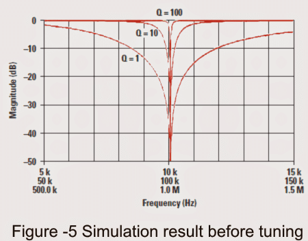
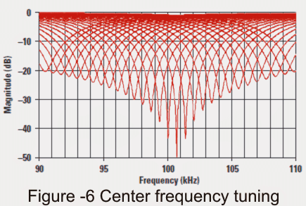 The collection of waveforms to the left and right of the center frequency (100.731 kHz) corresponds to filter reactions, once the 1-k¦¸ potentiometer is positioned and tweaked in 1% increments.
Every time the potentiometer is tuned halfway, the notch filter rejects frequencies at the precise core frequency.
The degree of the simulated notch is in fact on the order of 95 dB, however this is simply not supposed to materialize in the physical entity.
A 1% realignment of the potentiometer places a notch which is usually exceeding 40 dB straight on the preferred frequency.
Once again, this really may be the best scenario when done with ideal components, nevertheless lab data show more accurate at lower frequencies (10 and 100 kHz).
Figure 6 determines that you need to achieve a much closer to the precise frequency with R0 and C0 at the very start.
As the potentiometer may be able to rectify frequencies over an extensive spectrum, the depth of the notch could degrade.
Over a modest range (ˇŔ1%), one may achieve a 100:1 rejection of the bad frequency; nevertheless over an increased range (ˇŔ10%), only a 10:1 rejection is feasible.
The collection of waveforms to the left and right of the center frequency (100.731 kHz) corresponds to filter reactions, once the 1-k¦¸ potentiometer is positioned and tweaked in 1% increments.
Every time the potentiometer is tuned halfway, the notch filter rejects frequencies at the precise core frequency.
The degree of the simulated notch is in fact on the order of 95 dB, however this is simply not supposed to materialize in the physical entity.
A 1% realignment of the potentiometer places a notch which is usually exceeding 40 dB straight on the preferred frequency.
Once again, this really may be the best scenario when done with ideal components, nevertheless lab data show more accurate at lower frequencies (10 and 100 kHz).
Figure 6 determines that you need to achieve a much closer to the precise frequency with R0 and C0 at the very start.
As the potentiometer may be able to rectify frequencies over an extensive spectrum, the depth of the notch could degrade.
Over a modest range (ˇŔ1%), one may achieve a 100:1 rejection of the bad frequency; nevertheless over an increased range (ˇŔ10%), only a 10:1 rejection is feasible.
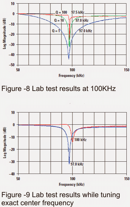
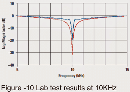 The opamp was without a doubt reducing the notch deepness at a center frequency of 100 kHz! A 32-dB notch is a cancellation of 40:1, that could be reasonably decent.
Therefore in spite of parts that engineered a preliminary 4% error, it had been easy to churn out a 32-dB notch at the most wanted center frequency.
The unpleasant news is the fact that to evade opamp bandwidth constraints, the highest possible notch frequency conceivable with a 100-MHz opamp is approximately 10 and 100 kHz.
When it comes to notch filters, ˇ°high-speedˇ± is accordingly considered genuine at around hundreds of kilohertz.
A superb practical application for 10-kHz notch filters is AM (medium-wave) receivers, in which the carrier from neighboring stations generates a loud 10-kHz screech in the audio, specifically during the night.
This could certainly grate on oneˇŻs nerves while tuning in is continuous.
Figure 11 displays the picked up audio spectrum of a station without using and using the 10-kHz notch was implemented.
Notice that the 10-kHz noise is the most loud section of the picked up audio (Figure 11a), even though the human ear is substantially less susceptible to it.
The opamp was without a doubt reducing the notch deepness at a center frequency of 100 kHz! A 32-dB notch is a cancellation of 40:1, that could be reasonably decent.
Therefore in spite of parts that engineered a preliminary 4% error, it had been easy to churn out a 32-dB notch at the most wanted center frequency.
The unpleasant news is the fact that to evade opamp bandwidth constraints, the highest possible notch frequency conceivable with a 100-MHz opamp is approximately 10 and 100 kHz.
When it comes to notch filters, ˇ°high-speedˇ± is accordingly considered genuine at around hundreds of kilohertz.
A superb practical application for 10-kHz notch filters is AM (medium-wave) receivers, in which the carrier from neighboring stations generates a loud 10-kHz screech in the audio, specifically during the night.
This could certainly grate on oneˇŻs nerves while tuning in is continuous.
Figure 11 displays the picked up audio spectrum of a station without using and using the 10-kHz notch was implemented.
Notice that the 10-kHz noise is the most loud section of the picked up audio (Figure 11a), even though the human ear is substantially less susceptible to it.
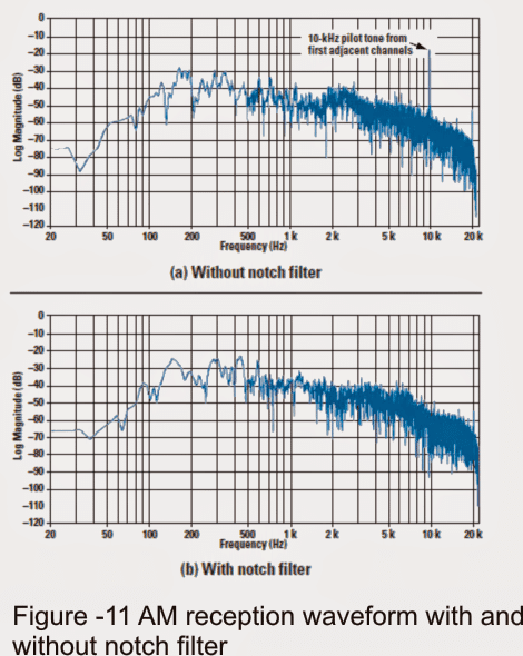 This audio range was captured at nighttime on a nearby station that received a couple of powerful stations on both side.
FCC stipulations permit certain variance of the station carriers.
For that reason, modest pitfalls in carrier frequency of the two neighboring stations is likely to make the 10-kHz noises heterodyne, boosting the annoying listening experience.
Whenever the notch filter is implemented (Figure 11b), the 10-kHz tone is minimized to the matching level as that of the adjacent modulation.
Furthermore observable on the audio spectrum are 20-kHz carriers from stations 2 channels away and a 16-kHz tone from a transatlantic station.
These are generally not a big concern, since they are attenuated considerably by the receiver IF.
A frequency at around 20 kHz may be inaudible to the overwhelming majority of individuals in either case.
References:
http://www.ti.com/lit/an/snoa680/snoa680.pdf
http://www.ti.com/lit/an/sbfa012/sbfa012.pdf
http://www.ti.com/lit/an/slyt235/slyt235.pdf
https://en.wikipedia.org/wiki/Band-stop_filter
This audio range was captured at nighttime on a nearby station that received a couple of powerful stations on both side.
FCC stipulations permit certain variance of the station carriers.
For that reason, modest pitfalls in carrier frequency of the two neighboring stations is likely to make the 10-kHz noises heterodyne, boosting the annoying listening experience.
Whenever the notch filter is implemented (Figure 11b), the 10-kHz tone is minimized to the matching level as that of the adjacent modulation.
Furthermore observable on the audio spectrum are 20-kHz carriers from stations 2 channels away and a 16-kHz tone from a transatlantic station.
These are generally not a big concern, since they are attenuated considerably by the receiver IF.
A frequency at around 20 kHz may be inaudible to the overwhelming majority of individuals in either case.
References:
http://www.ti.com/lit/an/snoa680/snoa680.pdf
http://www.ti.com/lit/an/sbfa012/sbfa012.pdf
http://www.ti.com/lit/an/slyt235/slyt235.pdf
https://en.wikipedia.org/wiki/Band-stop_filter
 The value of R1 will depend on the speaker impedance rating, for 8 ohms it will be 18k, for 4 ohms it should be 10k, and for 16 ohms it may be increased to 30k approximately.
The IC is LED bar/dot mode sequential driver device, in which the connected LEDs illuminate or "run" back-forth sequentially across the shown array (yellow to red), in response to a rising/falling voltage across its pin#5.
As can be seen in the diagram, the pin#5 is linked with the subwoofer speaker terminal via a voltage divider network R1 and R2.
R2 is in the form of a preset which is adjusted to set the full 10 LED range illumination for a given maximum magnitude of input signal at the pin#5 of the IC.
The above design can also be effectively substituted for illuminating EL wire lights, by implementing a few modification in the circuit.
The value of R1 will depend on the speaker impedance rating, for 8 ohms it will be 18k, for 4 ohms it should be 10k, and for 16 ohms it may be increased to 30k approximately.
The IC is LED bar/dot mode sequential driver device, in which the connected LEDs illuminate or "run" back-forth sequentially across the shown array (yellow to red), in response to a rising/falling voltage across its pin#5.
As can be seen in the diagram, the pin#5 is linked with the subwoofer speaker terminal via a voltage divider network R1 and R2.
R2 is in the form of a preset which is adjusted to set the full 10 LED range illumination for a given maximum magnitude of input signal at the pin#5 of the IC.
The above design can also be effectively substituted for illuminating EL wire lights, by implementing a few modification in the circuit.
 In the above diagram the transistors bases needs to be hooked up with the IC output pinouts from pin#1, and pin#10 to pin#18.
The common top connection of the Electroluminescent Wires can be seen connected with a boost AC supply derived from a boost inverter.
This boost converter can be quite easily made by assembling any standard boost converter circuit, such as a IC 555 boost circuit.
I'll be discussing this elaborately soon in one of my future articles in this blog.
In the above shown driver circuit, the transistor bases are fed with a sequentially fluctuating negative signals from the IC in response to the subwoofer bass beats pulses, which switch off the transistors at the same pattern, forcing the SCRs to turn ON with the same effect.
This in turn produces a sequentially "running" push-pull show across the entire Electroluminescent Wire string,
In the above diagram the transistors bases needs to be hooked up with the IC output pinouts from pin#1, and pin#10 to pin#18.
The common top connection of the Electroluminescent Wires can be seen connected with a boost AC supply derived from a boost inverter.
This boost converter can be quite easily made by assembling any standard boost converter circuit, such as a IC 555 boost circuit.
I'll be discussing this elaborately soon in one of my future articles in this blog.
In the above shown driver circuit, the transistor bases are fed with a sequentially fluctuating negative signals from the IC in response to the subwoofer bass beats pulses, which switch off the transistors at the same pattern, forcing the SCRs to turn ON with the same effect.
This in turn produces a sequentially "running" push-pull show across the entire Electroluminescent Wire string,
 Once done, the indicated AC lamps would start sequencing up and down in a dancing mode in response to the fed input music creating a dazzling DJ music lamp effect.
WARNING: THE ABOVE CONCEPT IS NOT ISOLATED FROM MAINS AC, THEREFORE MAY BE LETHAL TO TOUCH IN OPEN AND POWERED CONDITION.
EXERCISE EXTREME CAUTION WHILE TESTING AND HANDLING THIS UNIT.
Once done, the indicated AC lamps would start sequencing up and down in a dancing mode in response to the fed input music creating a dazzling DJ music lamp effect.
WARNING: THE ABOVE CONCEPT IS NOT ISOLATED FROM MAINS AC, THEREFORE MAY BE LETHAL TO TOUCH IN OPEN AND POWERED CONDITION.
EXERCISE EXTREME CAUTION WHILE TESTING AND HANDLING THIS UNIT.
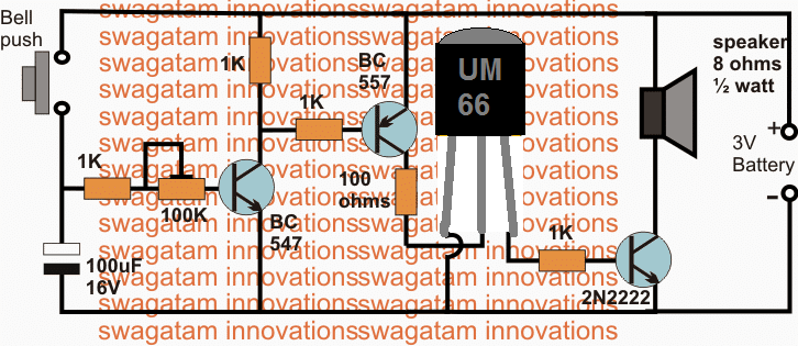 The diagram above depicts the proposed musical door bell circuit, the various stages may be understood with the following explanation.
The BC547 transistor along with the associated preset and the 100uF capacitor form a simple delay OFF timer circuit, where the preset and the capacitor determines the delay for which the sound output may be sustained once the indicated push button is pressed momentarily.
The diagram above depicts the proposed musical door bell circuit, the various stages may be understood with the following explanation.
The BC547 transistor along with the associated preset and the 100uF capacitor form a simple delay OFF timer circuit, where the preset and the capacitor determines the delay for which the sound output may be sustained once the indicated push button is pressed momentarily.
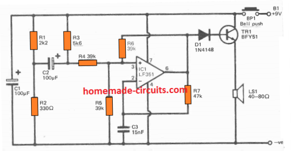 The above door buzzer circuit will produce a sharp buzzing sound whenever the push button is pressed by any guest at the door.
This design is suitable for users who do not wish to have a musical sound, instead prefer a buzzer kind of sound which sustains only as long as the button remain depressed.
The circuit is basically a square wave oscillator built around the op amp LM351. You can actually use any op amp instead of the specified one.
The parts C3, R7 decide the oscillation frequency which in turn produces the required buzzer door bell sound on the connected loudspeaker.
TR1 can be also replaced by any 1 amp NPN transistor if the specified number is not available.
The above door buzzer circuit will produce a sharp buzzing sound whenever the push button is pressed by any guest at the door.
This design is suitable for users who do not wish to have a musical sound, instead prefer a buzzer kind of sound which sustains only as long as the button remain depressed.
The circuit is basically a square wave oscillator built around the op amp LM351. You can actually use any op amp instead of the specified one.
The parts C3, R7 decide the oscillation frequency which in turn produces the required buzzer door bell sound on the connected loudspeaker.
TR1 can be also replaced by any 1 amp NPN transistor if the specified number is not available.
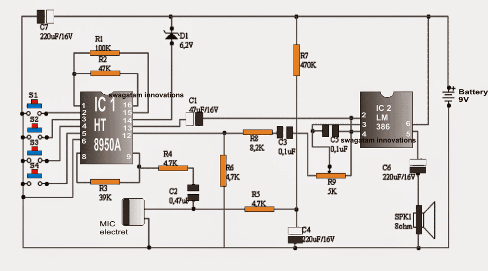 If you have problems with the above design, you can built the following original circuit from the datasheet of HT 8950.
You can replace the audio amplifier section with any other compatible amplifier circuit of your choice.
If you have problems with the above design, you can built the following original circuit from the datasheet of HT 8950.
You can replace the audio amplifier section with any other compatible amplifier circuit of your choice.
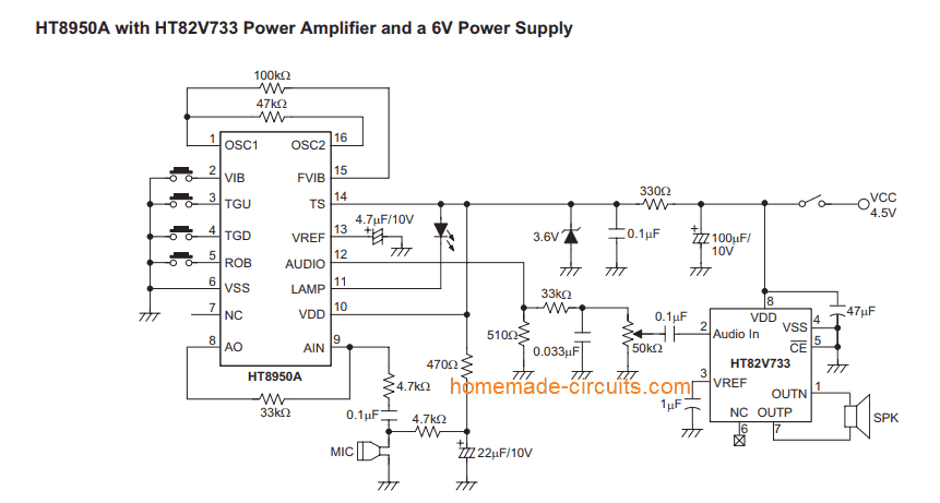
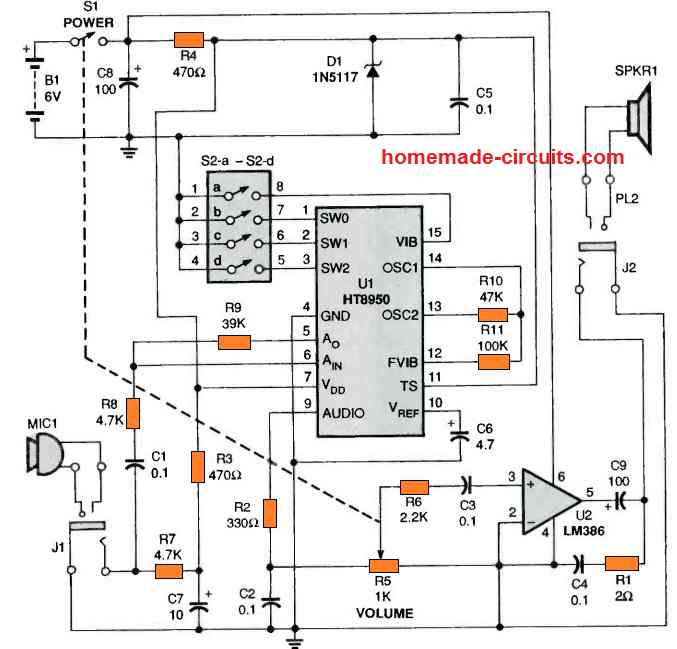 Four dry cells generate the required 6 V for operating the LM386 audio amplifier, U2. Resistor R4 and Zener-diode D1 are used for stepping down and controlling the battery voltage to 3.6 V to operate the HT8950 signal-processor device, U1. S1 is the power switch which is also the integrated part of the volume-control potentiometer, R5. Capacitors C8 and C5 deliver smoothing of the DC supply for the circuit.
While using the voice modulator circuit, the voice signal is detected by electret MIC1 and the signal is AC coupled by capacitor C1 to pin#6 of the IC U1 (pin#6 is the input pin of the IC's preamplifier stage).
Resistors R8 and R9 are configured to fix the gain of the internal preamplifier to around 8, which is determined by the equation:
Vout = (R9/R9) x Vin
The output preamplifier stage of the IC after passing through a buffer stgae is applied to the chip's internal, 8 -bit, analog-to-digital converter.
That voice signal is then sampled by the converter at 8 kHz through a time-base generator.
Also, the internal SRAM memory saves the 8-bit digital figures in it.
At the same time, the control circuit of the IC control provides the clock pulses to the SRAM data out to a digital-to-analog converter (DAC).
This stage subsequently reproduces the analog voice signal through the output pin 9.
The processed signal after this moves via a low-pass filter created through the amplification via R5 which finally drives the loudspeaker SPKR1. The potentiometer R5 is used for controlling the volume of the output modulated voice signal.
If the speech information is switched in and out of U1's SRAM with precisely the same frequency, the original voice signal gets reproduced without any modulations or changes.
However in case the digital information is modified prior to transferring it via the DAC, some very bizarre sound effects could be generated! The 4-step DIP switch, S2, is employed to establish the working modes of the IC HT8950 (see Table 1).
Four dry cells generate the required 6 V for operating the LM386 audio amplifier, U2. Resistor R4 and Zener-diode D1 are used for stepping down and controlling the battery voltage to 3.6 V to operate the HT8950 signal-processor device, U1. S1 is the power switch which is also the integrated part of the volume-control potentiometer, R5. Capacitors C8 and C5 deliver smoothing of the DC supply for the circuit.
While using the voice modulator circuit, the voice signal is detected by electret MIC1 and the signal is AC coupled by capacitor C1 to pin#6 of the IC U1 (pin#6 is the input pin of the IC's preamplifier stage).
Resistors R8 and R9 are configured to fix the gain of the internal preamplifier to around 8, which is determined by the equation:
Vout = (R9/R9) x Vin
The output preamplifier stage of the IC after passing through a buffer stgae is applied to the chip's internal, 8 -bit, analog-to-digital converter.
That voice signal is then sampled by the converter at 8 kHz through a time-base generator.
Also, the internal SRAM memory saves the 8-bit digital figures in it.
At the same time, the control circuit of the IC control provides the clock pulses to the SRAM data out to a digital-to-analog converter (DAC).
This stage subsequently reproduces the analog voice signal through the output pin 9.
The processed signal after this moves via a low-pass filter created through the amplification via R5 which finally drives the loudspeaker SPKR1. The potentiometer R5 is used for controlling the volume of the output modulated voice signal.
If the speech information is switched in and out of U1's SRAM with precisely the same frequency, the original voice signal gets reproduced without any modulations or changes.
However in case the digital information is modified prior to transferring it via the DAC, some very bizarre sound effects could be generated! The 4-step DIP switch, S2, is employed to establish the working modes of the IC HT8950 (see Table 1).
 For controlling single LEDs or multiple LEDs from separate Arduino outputs, individual mosfets may be required as given below:
 The LED resistors may be calculated using the following formula:
R = (U - LEDfwdV)/LED Current
where U is the supply voltage
LEDfwdV is the LED forward operating voltage of the particular series
LED current is the ampere rating specs of the LEDs used
Therefore here U = 12V
LEDfwdV = 3.3V x 3 = 9.9V since 3nos are there in each series and 3.3V being the forward voltage spec of each LED
LED current = 350mA, let's take it 300mA or 0.3Amp to keep things cooler.
Substituting these in the formula:
R = (U - LEDfwdV)/LED Current
= 12 - 9.9/0.3
= 7 ohm
watts may be calculated as
Watts = LEDfwdV x LED current = 9.9 x 0.3 = 2.97 watts or 3 watts
The LED resistors may be calculated using the following formula:
R = (U - LEDfwdV)/LED Current
where U is the supply voltage
LEDfwdV is the LED forward operating voltage of the particular series
LED current is the ampere rating specs of the LEDs used
Therefore here U = 12V
LEDfwdV = 3.3V x 3 = 9.9V since 3nos are there in each series and 3.3V being the forward voltage spec of each LED
LED current = 350mA, let's take it 300mA or 0.3Amp to keep things cooler.
Substituting these in the formula:
R = (U - LEDfwdV)/LED Current
= 12 - 9.9/0.3
= 7 ohm
watts may be calculated as
Watts = LEDfwdV x LED current = 9.9 x 0.3 = 2.97 watts or 3 watts
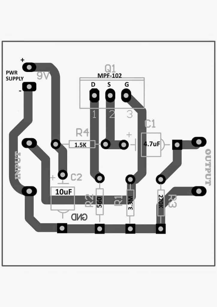 Following are the images of the DIY contact mic prototype, built and submitted by Mr.Ajay Dusa
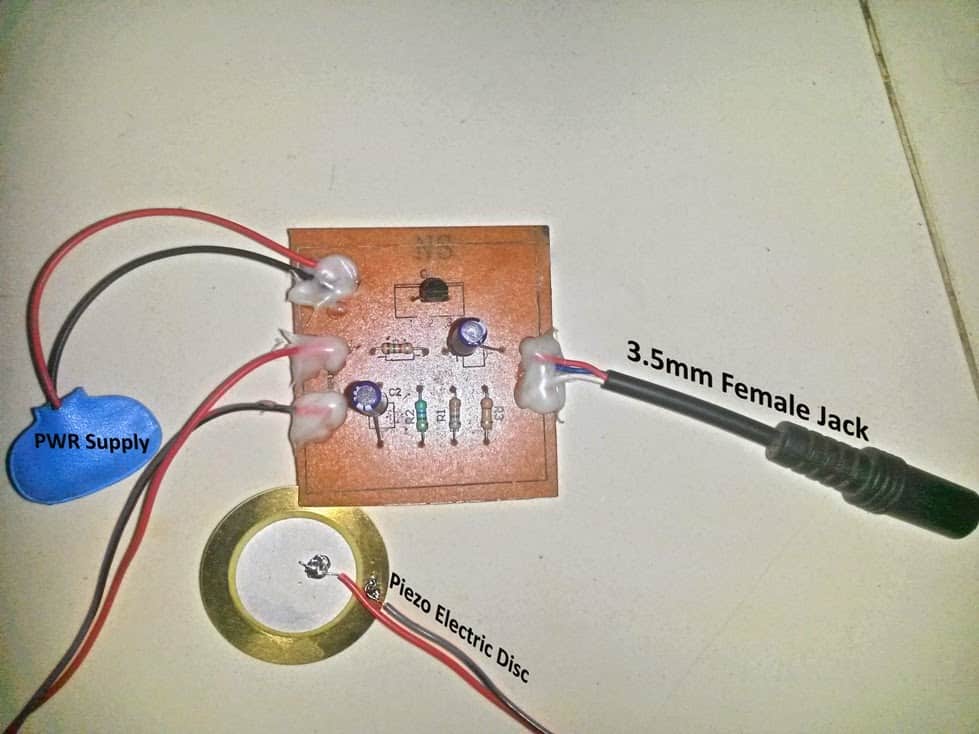
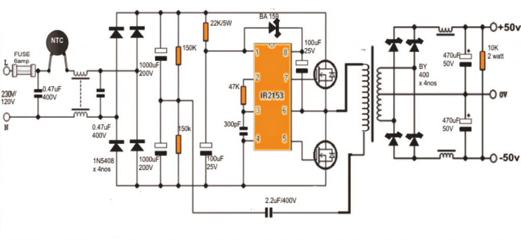
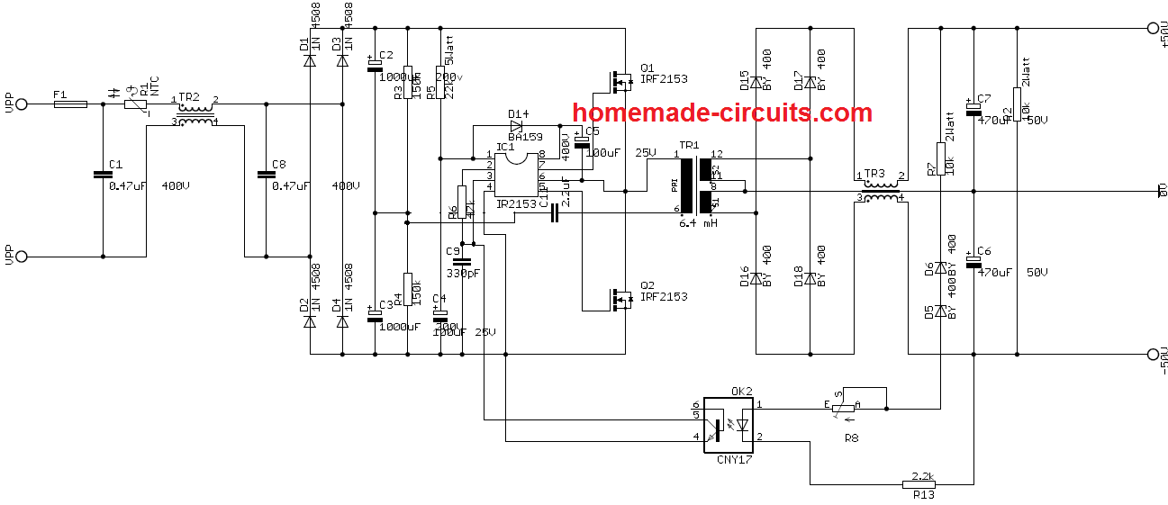
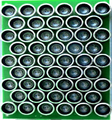
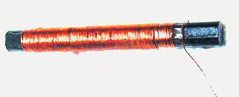
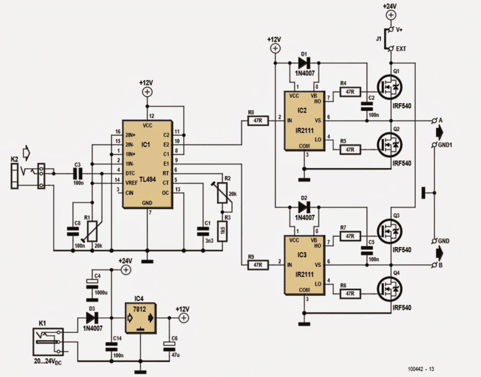 Circuit idea courtesy: Elektor electronics.
In my prototype I experimented with an audio transformer as shown below for the required amplification, with a single common 12V supply.
I did not use any resonant capacitors therefore the amplification was too low.
I could hear the effect from a distance of 1 feet exactly across a straight line with the transducer.
Even a slight movement caused the sound to disappear.
Circuit idea courtesy: Elektor electronics.
In my prototype I experimented with an audio transformer as shown below for the required amplification, with a single common 12V supply.
I did not use any resonant capacitors therefore the amplification was too low.
I could hear the effect from a distance of 1 feet exactly across a straight line with the transducer.
Even a slight movement caused the sound to disappear.
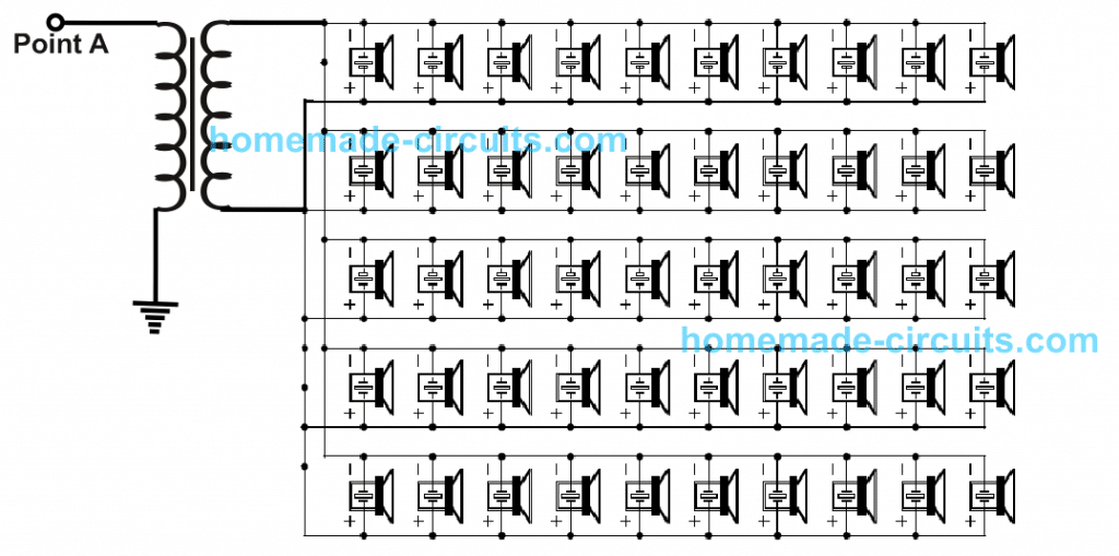 Transducer wiring details can be seen in the below given figure, you will need two of these set-ups to be connected with points A and B of the circuit.
The transformer can be suitable step up transformer depending on how many transducers are selected.
Prototype Image: The above parametric speaker circuit was successfully tested and confirmed by me using 4 ultrasonic transducers, which responded exactly as specified in the article explanation.
However, since only 4 sensors were used the output was too low and could be heard only from a meter away.
Transducer wiring details can be seen in the below given figure, you will need two of these set-ups to be connected with points A and B of the circuit.
The transformer can be suitable step up transformer depending on how many transducers are selected.
Prototype Image: The above parametric speaker circuit was successfully tested and confirmed by me using 4 ultrasonic transducers, which responded exactly as specified in the article explanation.
However, since only 4 sensors were used the output was too low and could be heard only from a meter away.
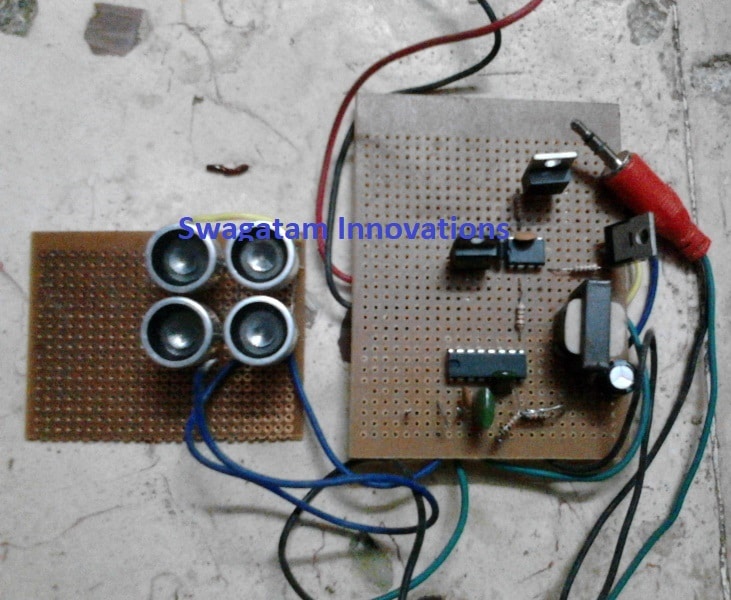 Caution ˇŞ Health Hazard.
Appropriate measures must be taken to prevent long term exposure to high ultrasonic sound levels.
Original Document can be Read Here
Caution ˇŞ Health Hazard.
Appropriate measures must be taken to prevent long term exposure to high ultrasonic sound levels.
Original Document can be Read Here
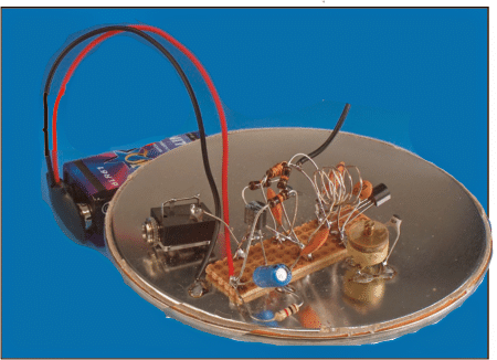 Image Courtesy: Elektor Electronics
It's basically based on a superregenerative audion receiver circuit where the use of minimal components becomes the main feature of the unit.
However fewer components also means a few compromises involved, here the receiver requires a large metal base for grounding the unwanted signals, and for keeping the noise factor to the lowest, and also this system would work only in places where the reception is rather strong and thus may not be suitable in areas where the signal strength is thinner.
Image Courtesy: Elektor Electronics
It's basically based on a superregenerative audion receiver circuit where the use of minimal components becomes the main feature of the unit.
However fewer components also means a few compromises involved, here the receiver requires a large metal base for grounding the unwanted signals, and for keeping the noise factor to the lowest, and also this system would work only in places where the reception is rather strong and thus may not be suitable in areas where the signal strength is thinner.
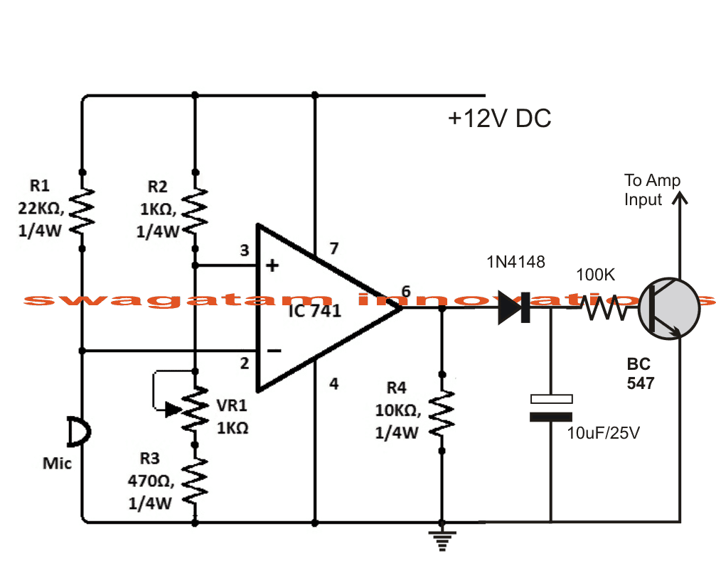
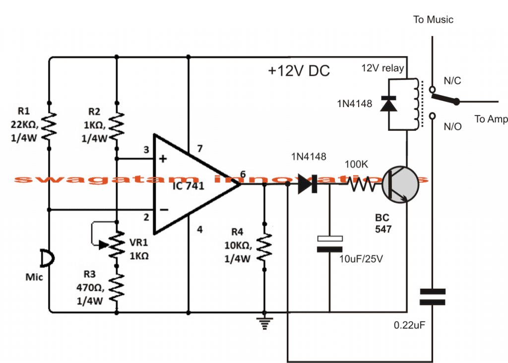

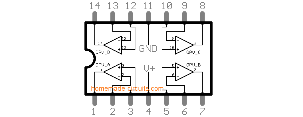 Please make sure to connect the pin#4 of the ICs with the (+) DC supply, and the pin#11 with the 0V of the power supply and the circuit 0V line
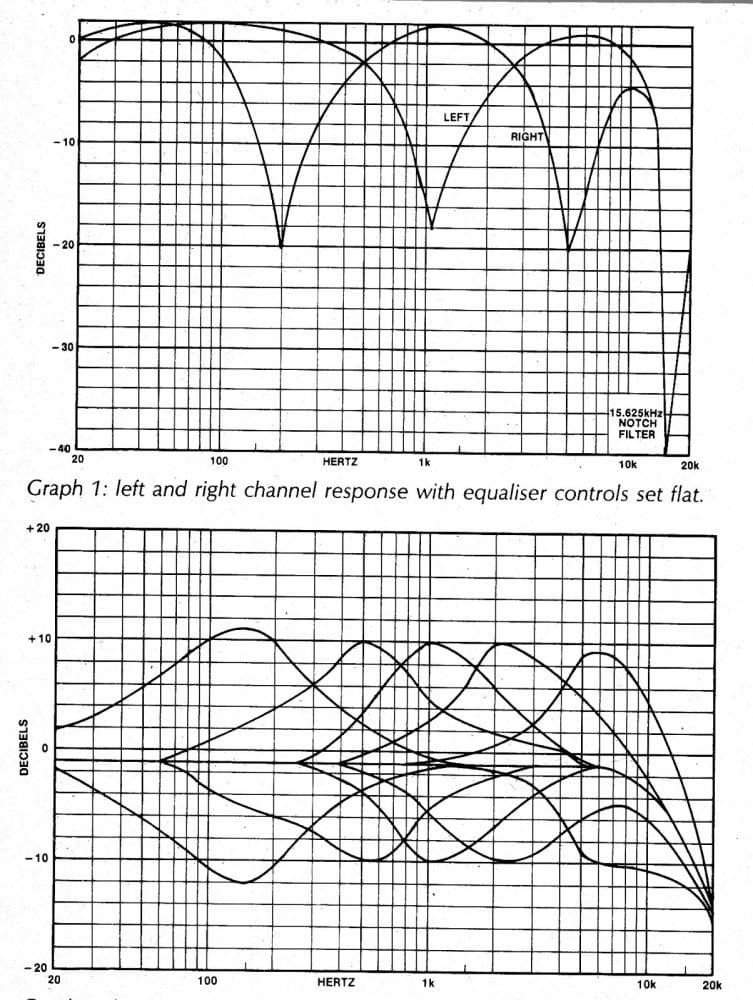
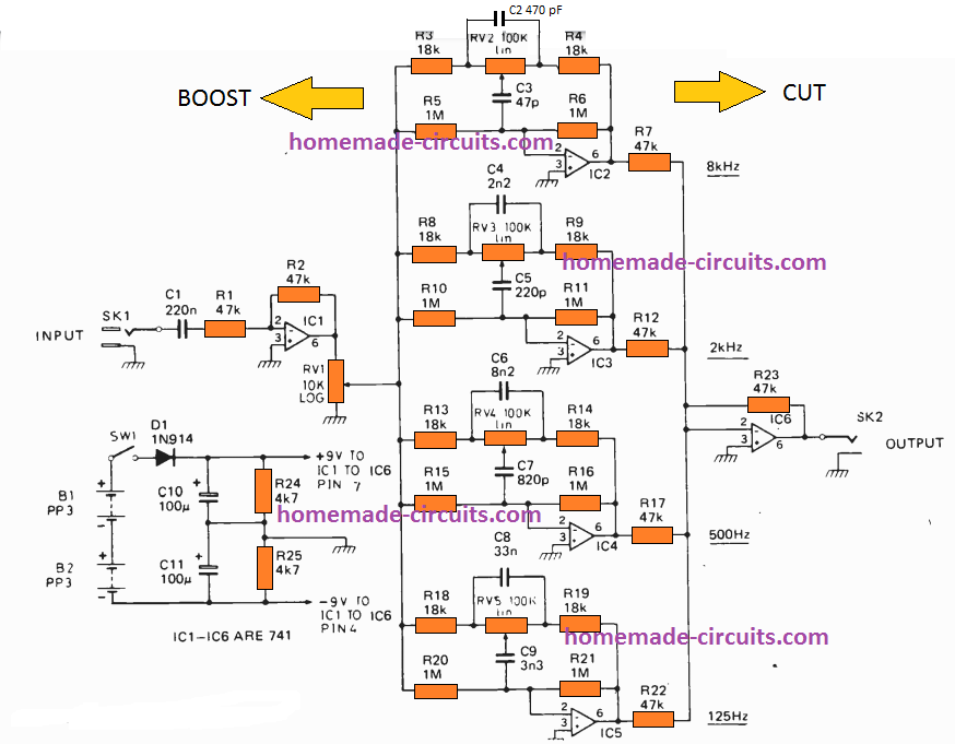 Parts List
RESISTORS all 1/4W, 5%
R1, R2 = 47k
R3, R4 = 18k
R5, R6 = 1M
R7 = 47k
R8, R9 =18k
R10, R11 = 1M
R12 = 47k
R13, R14 = 18k
R15, R16 = 1M
R17 = 47k
R18, R19 = 18k
R20, R21 = 1M
R22, R23 = 47k
R24, R25 = 4k7
POTENTIOMETERS
RV1 10k log slider pot
RV2, 3, 4, 5 ˇ .
100k linear slider pot
CAPACITORS
C1 = 220n PPC
C2 = 470p PPC
C3 = 47p ceramic
C4 = 2n2 PPC
C5 = 220p ceramic
C6 = 8n2 PPC
C7 = 820p ceramic
C8 = 33n PPC
C9 = 3n3 PPC
C10, C11 = 100¦Ě 25V electrolytic
SEMICONDUCTORS
IC1-1C6 = 741 op amp
D1 = IN914 or 1N4148
MISCELLANEOUS
SW1 spst miniature toggle switch
SKI, 2 mono jack sockets
B1, 2 9V 216 batteries
Parts List
RESISTORS all 1/4W, 5%
R1, R2 = 47k
R3, R4 = 18k
R5, R6 = 1M
R7 = 47k
R8, R9 =18k
R10, R11 = 1M
R12 = 47k
R13, R14 = 18k
R15, R16 = 1M
R17 = 47k
R18, R19 = 18k
R20, R21 = 1M
R22, R23 = 47k
R24, R25 = 4k7
POTENTIOMETERS
RV1 10k log slider pot
RV2, 3, 4, 5 ˇ .
100k linear slider pot
CAPACITORS
C1 = 220n PPC
C2 = 470p PPC
C3 = 47p ceramic
C4 = 2n2 PPC
C5 = 220p ceramic
C6 = 8n2 PPC
C7 = 820p ceramic
C8 = 33n PPC
C9 = 3n3 PPC
C10, C11 = 100¦Ě 25V electrolytic
SEMICONDUCTORS
IC1-1C6 = 741 op amp
D1 = IN914 or 1N4148
MISCELLANEOUS
SW1 spst miniature toggle switch
SKI, 2 mono jack sockets
B1, 2 9V 216 batteries
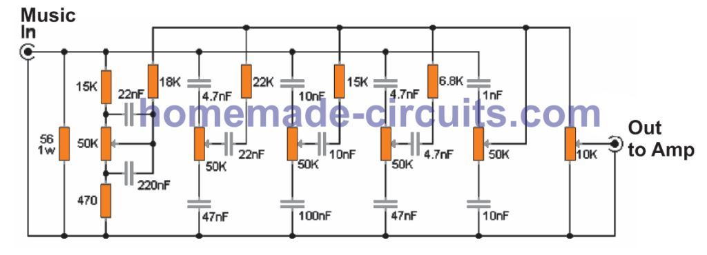 As can be seen in the figure above, the 5 band equalizer has five potentiometers for controlling the tone of the input music signal, while the sixth potentiometer is positioned for controlling the volume of the sound output.
Basically, the shown stages are simple RC filters, which narrow or broaden the frequency passage of the input signal, so that only a certain band of frequency is allowed to pass, depending on the adjustment of the relevant pots.
The equalized frequency bands are 60Hz, 240Hz, 1KHz, 4KHz and 16KHz, from left towards right.Lastly followed by the volume control pot control.
Since the design does not use active components this equalizer is able to operate without any supply input.Please note that if this 5 band equalizer is implemented for a stereo or multichannel system, it may become necessary to set up an equalizer in the identical manner for each of the channels.
As can be seen in the figure above, the 5 band equalizer has five potentiometers for controlling the tone of the input music signal, while the sixth potentiometer is positioned for controlling the volume of the sound output.
Basically, the shown stages are simple RC filters, which narrow or broaden the frequency passage of the input signal, so that only a certain band of frequency is allowed to pass, depending on the adjustment of the relevant pots.
The equalized frequency bands are 60Hz, 240Hz, 1KHz, 4KHz and 16KHz, from left towards right.Lastly followed by the volume control pot control.
Since the design does not use active components this equalizer is able to operate without any supply input.Please note that if this 5 band equalizer is implemented for a stereo or multichannel system, it may become necessary to set up an equalizer in the identical manner for each of the channels.
 Audio input is sent from left side at the input of C1, while the enhanced equalizer effect is acquired from the right side R4 end which must be connected to the power amplifier.
The dotted lines indicate that the relevant potentiometers must be dual type pots, and must move concurrently.
The effect from such parametric equalizers or filter circuit is said to be similar to the effects that we normally get in concert halls, and auditoriums.
Audio input is sent from left side at the input of C1, while the enhanced equalizer effect is acquired from the right side R4 end which must be connected to the power amplifier.
The dotted lines indicate that the relevant potentiometers must be dual type pots, and must move concurrently.
The effect from such parametric equalizers or filter circuit is said to be similar to the effects that we normally get in concert halls, and auditoriums.
 If you are interested to create your own low pass filter with a single IC 741 and customize it, then the following discussion might help!
 For technical explanation of the circuit you may refer to the data provided here.
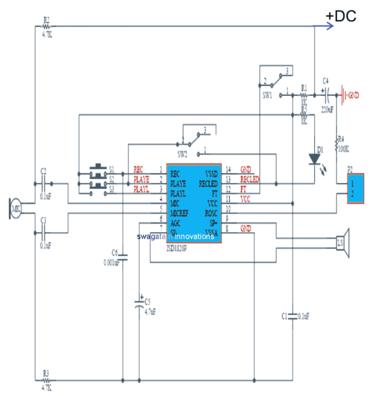 Referring to the proposed 20 second message record/playback circuit diagram using the IC ISD1820:
1) Pin#1 can be seen as the REC (recording) input pinout, which accepts a positive signal for enabling the recording function, meaning this pinout must be connected to the Vcc or the positive line while recording an audio clip,
The REC pinout has the ability to take precedence over the other pinouts marked PLAYE/PLAYL in case it is pulled high while any of the other pinouts were functioning.
Meaning suppose if any of the PLAY button was pressed, and simultaneously REC was pressed, in such case the recording (REC) will be immediately initiated terminating the PLAY action.
The voice recording action can be stopped as soon the relevant button is switched OFF, and the REC pinout is rendered at LOW.
In this position an internal EOM or end of message prompt is triggered internally, causing the PLAYBACK mode to get in the ready position.
This also causes the chip to go into a power down condition or in the standby condition.
2) PLAY pinouts: As can be noticed in the diagram, the IC facilitates two PLAY pinouts, which are PLAYE, and PLAYL.
PLAYE allows an logic edge activated triggering, while PLAYL facilitates a logic-level activated triggering of the playback.
In the PLAY E or edge activated mode, a single press and release or a momentary press of the button will initiate the playback of the recorded clipping through the speaker, and will end as soon as the internal EOM (end of message) signal gets activated.
The PLAY L mode is activated when the attached button is pressed and held pressed without releasing it.
The audio playback now continues as long as the button remains depressed, or as soon as the internal EOM is activated.
Keeping the button permanently pressed will cause a higher current consumption of the IC.
Other than the REC and the PLAY buttons, this audio record/playback circuit additionally possesses a couple of switches associated with the chip in the form of SW1 and SW2. SW1 is positioned for the ˇ°Feed Throughˇ± action while SW2 for the ˇ°REPEATˇ± functioning.
LetˇŻs understand them in detail.
As may be witnessed, the SW1 is configured with the ˇ°FTˇ± pinout of the IC which refers to ˇ°Feed Throughˇ±.
When actuated in the feed through mode, the signal across MIC, and the MIC_REF pinouts are bypassed through the AGC pinout of the IC, up to the the filter driver stage and finally reaching the speaker points (SP+ and SP-)
The FT input signal is responsible for controlling the feed through mode of the chip.
In order to be initiated the feed through mode, the pinout FT is held at the positive Vcc logic, while the REC, and the PLAY buttons are at low logic or with their buttons in the deactivated positions.
SW2 is used for enabling the REPEAT mode, which implies that when this switch is toggled ON the playback goes on repeating the recorded message clip through the speaker non-stop, until the switch is toggled OFF.
Referring to the proposed 20 second message record/playback circuit diagram using the IC ISD1820:
1) Pin#1 can be seen as the REC (recording) input pinout, which accepts a positive signal for enabling the recording function, meaning this pinout must be connected to the Vcc or the positive line while recording an audio clip,
The REC pinout has the ability to take precedence over the other pinouts marked PLAYE/PLAYL in case it is pulled high while any of the other pinouts were functioning.
Meaning suppose if any of the PLAY button was pressed, and simultaneously REC was pressed, in such case the recording (REC) will be immediately initiated terminating the PLAY action.
The voice recording action can be stopped as soon the relevant button is switched OFF, and the REC pinout is rendered at LOW.
In this position an internal EOM or end of message prompt is triggered internally, causing the PLAYBACK mode to get in the ready position.
This also causes the chip to go into a power down condition or in the standby condition.
2) PLAY pinouts: As can be noticed in the diagram, the IC facilitates two PLAY pinouts, which are PLAYE, and PLAYL.
PLAYE allows an logic edge activated triggering, while PLAYL facilitates a logic-level activated triggering of the playback.
In the PLAY E or edge activated mode, a single press and release or a momentary press of the button will initiate the playback of the recorded clipping through the speaker, and will end as soon as the internal EOM (end of message) signal gets activated.
The PLAY L mode is activated when the attached button is pressed and held pressed without releasing it.
The audio playback now continues as long as the button remains depressed, or as soon as the internal EOM is activated.
Keeping the button permanently pressed will cause a higher current consumption of the IC.
Other than the REC and the PLAY buttons, this audio record/playback circuit additionally possesses a couple of switches associated with the chip in the form of SW1 and SW2. SW1 is positioned for the ˇ°Feed Throughˇ± action while SW2 for the ˇ°REPEATˇ± functioning.
LetˇŻs understand them in detail.
As may be witnessed, the SW1 is configured with the ˇ°FTˇ± pinout of the IC which refers to ˇ°Feed Throughˇ±.
When actuated in the feed through mode, the signal across MIC, and the MIC_REF pinouts are bypassed through the AGC pinout of the IC, up to the the filter driver stage and finally reaching the speaker points (SP+ and SP-)
The FT input signal is responsible for controlling the feed through mode of the chip.
In order to be initiated the feed through mode, the pinout FT is held at the positive Vcc logic, while the REC, and the PLAY buttons are at low logic or with their buttons in the deactivated positions.
SW2 is used for enabling the REPEAT mode, which implies that when this switch is toggled ON the playback goes on repeating the recorded message clip through the speaker non-stop, until the switch is toggled OFF.
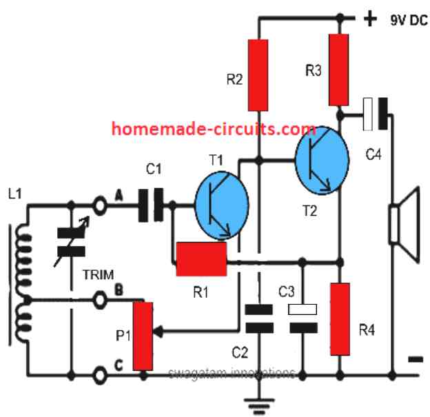
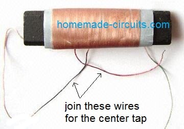 Use the Following type of GANG Condenser for the Trimmer (use the center pin and any one of the output pins from the MW side)
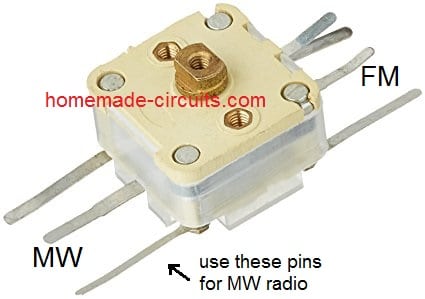
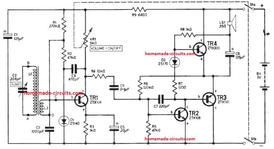 The transistors can be BC547 and BC557 for the NPN and the PNP respectively, while the diode can be 1N4148.
The Antenna Coil could be built using the following data:
The transistors can be BC547 and BC557 for the NPN and the PNP respectively, while the diode can be 1N4148.
The Antenna Coil could be built using the following data:
 The ferrite rod antenna coil picks up the AM frequency through the tuned network of C2, L1. The tuned AM signal is fed to the first transistor TR1 via L2.
This enables a correct matching of the high impedance input from C2, L1 with the transistor input, without causing any deteorioration of the tuned signal.
The signal gets amplified by TR1 and is fed to the detector stage made using the diode DI.
Here since the 470pF capacitor C4 responds with a lower impedance to the incoming r.f.
(radio frequency) than the 10 kilohm resistance R4, implies that the signal is now forced to enter through the capacitor C4.
This filters out the audio element in the signal after D1 detection, and is sent through the R2, L2 stage to the base of TR1.
C3 eliminates any form of stray RF.
Next is C4, which offers a high impedance to the signal compared to R4, which prompts the signal to move to TR2 base.
The ferrite rod antenna coil picks up the AM frequency through the tuned network of C2, L1. The tuned AM signal is fed to the first transistor TR1 via L2.
This enables a correct matching of the high impedance input from C2, L1 with the transistor input, without causing any deteorioration of the tuned signal.
The signal gets amplified by TR1 and is fed to the detector stage made using the diode DI.
Here since the 470pF capacitor C4 responds with a lower impedance to the incoming r.f.
(radio frequency) than the 10 kilohm resistance R4, implies that the signal is now forced to enter through the capacitor C4.
This filters out the audio element in the signal after D1 detection, and is sent through the R2, L2 stage to the base of TR1.
C3 eliminates any form of stray RF.
Next is C4, which offers a high impedance to the signal compared to R4, which prompts the signal to move to TR2 base.
 The next MW or AM receiver is actually so easy that really tiny expenditure is necessary for its construction, and as just a few number of parts are employed it is ideally suits a mini radio receiver, that effortlessly accommodates inside a shirt pocket.
Even so it provides very good reception of nearby radio stations with no need for an external antenna or earth wire.
The next MW or AM receiver is actually so easy that really tiny expenditure is necessary for its construction, and as just a few number of parts are employed it is ideally suits a mini radio receiver, that effortlessly accommodates inside a shirt pocket.
Even so it provides very good reception of nearby radio stations with no need for an external antenna or earth wire.
 Functioning of the receiver is extremely straightforward.
Transistor T1 works like an r.f.
amplifier and detector with regenerative (positive) feedback.
The level of feedback, and therefore the sensitivity of the MW receiver, could be manipulated by varying P1.
Even though output to the base of T1 is obtained straight from the upper section of the tuned circuit L1/C1, instead of through a coupling winding, the impedance offered by T1 is quite enough to make sure that the resonant circuit is barely suppressed.
Because the current gain of T1 decreases on the higher frequency side of the spectrum, while the input impedance rises, the gain of this stage continues to be relatively consistent on the entire spectrum, in order that it is normally not essential to fine-tune P1 often.
Signal detection happens on the collector of T1 and the output impedance of this T1 stage and C3, cleans out the r.f.
portion of the rectified signal.
T2 supplies further amplification of the a.f.
Signal to operate the attached crystal earpiece.
Functioning of the receiver is extremely straightforward.
Transistor T1 works like an r.f.
amplifier and detector with regenerative (positive) feedback.
The level of feedback, and therefore the sensitivity of the MW receiver, could be manipulated by varying P1.
Even though output to the base of T1 is obtained straight from the upper section of the tuned circuit L1/C1, instead of through a coupling winding, the impedance offered by T1 is quite enough to make sure that the resonant circuit is barely suppressed.
Because the current gain of T1 decreases on the higher frequency side of the spectrum, while the input impedance rises, the gain of this stage continues to be relatively consistent on the entire spectrum, in order that it is normally not essential to fine-tune P1 often.
Signal detection happens on the collector of T1 and the output impedance of this T1 stage and C3, cleans out the r.f.
portion of the rectified signal.
T2 supplies further amplification of the a.f.
Signal to operate the attached crystal earpiece.
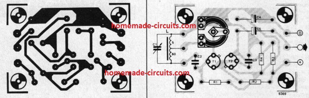 Individuals who want to miniaturize the layout even more may try things out by decreasing the measurements of the ferrite rod and adding more number of winding to obtain the very same inductance, while in case L1 is built smaller an external antenna could be required, which could be attached on the upper terminal of L1 through a 4.7 p capacitor.
The proposed dimensions for L1 will be 65 turns of 0.2 mm (36 S.W.G.) enameled copper wire over a 10 mm diameter 100 mm long ferrite rod, with the center tap coming out at 5 turns away from the `ground' end of the antenna coil.
C1 could be a small (strong dielectric) 500 pF gang condenser, or to get signals from a single fixed station only it might be substituted with a permanent capacitor of just lower than the necessary value in parallel with a 4 to 60 pF trimmer.
This may make it possible for the dimensions of the MW radio receiver to become additionally minimized.
Last but not least, the working current of the receiver is incredibly minimal that around 1 mA) in order that it will probably run for many months with a PP3 9 V battery.
Individuals who want to miniaturize the layout even more may try things out by decreasing the measurements of the ferrite rod and adding more number of winding to obtain the very same inductance, while in case L1 is built smaller an external antenna could be required, which could be attached on the upper terminal of L1 through a 4.7 p capacitor.
The proposed dimensions for L1 will be 65 turns of 0.2 mm (36 S.W.G.) enameled copper wire over a 10 mm diameter 100 mm long ferrite rod, with the center tap coming out at 5 turns away from the `ground' end of the antenna coil.
C1 could be a small (strong dielectric) 500 pF gang condenser, or to get signals from a single fixed station only it might be substituted with a permanent capacitor of just lower than the necessary value in parallel with a 4 to 60 pF trimmer.
This may make it possible for the dimensions of the MW radio receiver to become additionally minimized.
Last but not least, the working current of the receiver is incredibly minimal that around 1 mA) in order that it will probably run for many months with a PP3 9 V battery.
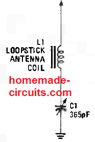 If the interfering signal comes from the lower frequency side of the broadcast band, you need to set L1ˇŻs slug around of the way into the coil and adjust C1 for a minimum signal output at the interfering frequency.
Once the interfering stationˇŻs frequency is close to the upper end of the band, regulate the slug until the end of the coil and tune C1 until you get a minimum signal.
It can happen that some unwanted transmitter signal besides a typical AM-broadcast type waves can get into the tank circuit.
When that happens, you must find out the transmitterˇŻs frequency and choose a coil/capacitor arrangement that will resonate at that frequency.
Then, connect that combination to the schematics above.
If the interfering signal comes from the lower frequency side of the broadcast band, you need to set L1ˇŻs slug around of the way into the coil and adjust C1 for a minimum signal output at the interfering frequency.
Once the interfering stationˇŻs frequency is close to the upper end of the band, regulate the slug until the end of the coil and tune C1 until you get a minimum signal.
It can happen that some unwanted transmitter signal besides a typical AM-broadcast type waves can get into the tank circuit.
When that happens, you must find out the transmitterˇŻs frequency and choose a coil/capacitor arrangement that will resonate at that frequency.
Then, connect that combination to the schematics above.
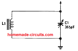 When the tuner is boosting the required level for the frequency, it is also suppressing all other signals outside its passband.
You can easily use the same combination of values for the capacitor and coil as depicted above..
Other kinds of antennas and selective circuits can be evaluated through the input of this tank circuit.
A huge tuned loop will provide the circuit an option to help reduce an interfering signal arriving from diverse directions.
If there isnˇŻt space for a big loop, you can opt for a large, tune ferrite coil as a replacement and hold its feature.
When the tuner is boosting the required level for the frequency, it is also suppressing all other signals outside its passband.
You can easily use the same combination of values for the capacitor and coil as depicted above..
Other kinds of antennas and selective circuits can be evaluated through the input of this tank circuit.
A huge tuned loop will provide the circuit an option to help reduce an interfering signal arriving from diverse directions.
If there isnˇŻt space for a big loop, you can opt for a large, tune ferrite coil as a replacement and hold its feature.
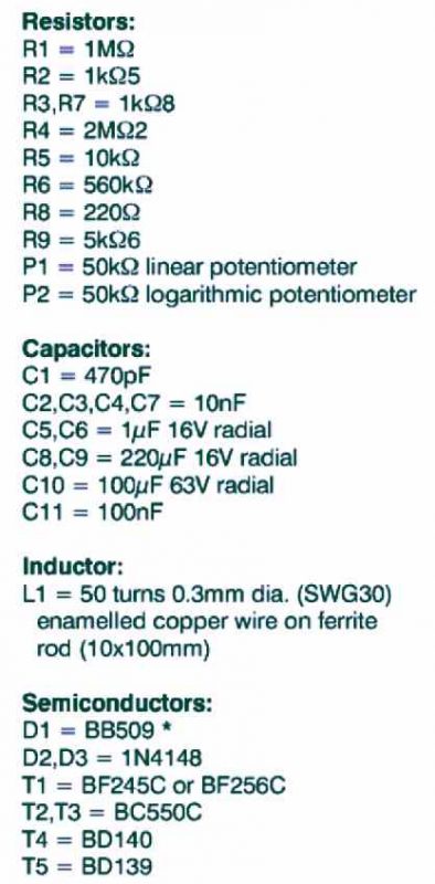
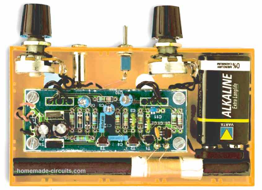 The antenna coil L1, the capacitor C1, and the diode D1 form the TRF MW receiver circuit or the main tuned receiver circuit stage.
C1 is a varicap diode whose capacitance varies depending on the voltage across it.
When the P1 is varied, it causes a voltage variation across C1, which in turn causes the tuning of the receiver and catching a various radio frequencies depending on the resonance formed by the C1 and L1.
Therefore varied P1 of the TRF receiver circuit allows to select the desired stations from the available incoming MW bands.
T1 and T2 along with the associated parts form the demodulator and the preamplifier stages, where T1 demodulates the resonant tuned frequency from the L1/C1 stage such that only the audio section is allowed to pass while the other unwanted voltages are blocked.
This tuned audio signal is fed to the preamplifier stage formed by T2 and the associated parts.
The pramplified radio audio is sent to the base of T3 via P2 and C6. P2 helps to set the volume of the output, and therefore works like a volume control pot.
The transistor T3 further amplifies the audio signal and forwards it to the power amplifier stage built around the transistors T4 and T5.
The T4, and T5 stage along with the other associated component form a nice little 1 watt transistorized amplifier that sufficiently amplifies the TRF audio signals, and feeds it to the attached loudspeaker.
The tuned MW radio output is thus effectively reproduced on the speaker loud and clear.
The antenna coil L1, the capacitor C1, and the diode D1 form the TRF MW receiver circuit or the main tuned receiver circuit stage.
C1 is a varicap diode whose capacitance varies depending on the voltage across it.
When the P1 is varied, it causes a voltage variation across C1, which in turn causes the tuning of the receiver and catching a various radio frequencies depending on the resonance formed by the C1 and L1.
Therefore varied P1 of the TRF receiver circuit allows to select the desired stations from the available incoming MW bands.
T1 and T2 along with the associated parts form the demodulator and the preamplifier stages, where T1 demodulates the resonant tuned frequency from the L1/C1 stage such that only the audio section is allowed to pass while the other unwanted voltages are blocked.
This tuned audio signal is fed to the preamplifier stage formed by T2 and the associated parts.
The pramplified radio audio is sent to the base of T3 via P2 and C6. P2 helps to set the volume of the output, and therefore works like a volume control pot.
The transistor T3 further amplifies the audio signal and forwards it to the power amplifier stage built around the transistors T4 and T5.
The T4, and T5 stage along with the other associated component form a nice little 1 watt transistorized amplifier that sufficiently amplifies the TRF audio signals, and feeds it to the attached loudspeaker.
The tuned MW radio output is thus effectively reproduced on the speaker loud and clear.
 The antenna coil L1, can be built by tightly winding 80 turns of 22 SWG enameled copper wire over a 3/8" diameter ferrite rod, and this works like the pickup coil.
The L1 is tuned through the 500pF trimmer and tank circuit tus formed is referenced to earth at the radio frequency by C1.
The high input impedance, offered by IC1/1, provided to the tank circuit guarantees that the damping factor is kept to the minimum, which causes the MW receiver circuit to be highly selective.
The output from the IC1/1 geneartes an amplified RF signal which is transferred to IC1/2 for the detection function.
The unwanted RF frequency generated at the output of the detector is eliminated by the low pass filter created by resistor R4 and capacitor C2. The output audio signal is subsequently provided to an amplifier constructed around IC1/3 and IC1/4.
The current consumption of the MW radio circuit's is around 10 mA while powered through a 9 V supply.
Remember that the IC used in this design has to be a 4011AE and not the 4011B whose input protection circuitry could prohibit it from running in the linear mode.
The antenna coil L1, can be built by tightly winding 80 turns of 22 SWG enameled copper wire over a 3/8" diameter ferrite rod, and this works like the pickup coil.
The L1 is tuned through the 500pF trimmer and tank circuit tus formed is referenced to earth at the radio frequency by C1.
The high input impedance, offered by IC1/1, provided to the tank circuit guarantees that the damping factor is kept to the minimum, which causes the MW receiver circuit to be highly selective.
The output from the IC1/1 geneartes an amplified RF signal which is transferred to IC1/2 for the detection function.
The unwanted RF frequency generated at the output of the detector is eliminated by the low pass filter created by resistor R4 and capacitor C2. The output audio signal is subsequently provided to an amplifier constructed around IC1/3 and IC1/4.
The current consumption of the MW radio circuit's is around 10 mA while powered through a 9 V supply.
Remember that the IC used in this design has to be a 4011AE and not the 4011B whose input protection circuitry could prohibit it from running in the linear mode.

 However this chip is even better as it requires very few external components for implementing the amplifier actions.
In the diagram we see that the input of the IC is connected to a small loudspeaker via a small output transformer.
The output of the IC is also connected to a loudspeaker.
A DPDT switch is configured and connected to the two speakers such that the whole circuit works like a two way intercom system.
The connectedloudspeakersact as a speech producing devices as well as mics for capturing soundsignalsfor amplification to the other end.
The right end speaker is the master while the speaker connected at the other end is for remote installation.
When the switch is positioned toward the talk mode, the master speakerbehavesas the mic, and the sound signal is announced and heard over the remote speaker.
When the switch is positioned toward the listen mode, all the conservation that might take place around the remote speaker istransferredand can be heard over the master speaker.
T1 is nothing but a small audio output transformer which may be easily procured from the market, thewindingwith lower impedance goes to the speaker while the side with the higher impedance gets connected to the input of the IC.
However this chip is even better as it requires very few external components for implementing the amplifier actions.
In the diagram we see that the input of the IC is connected to a small loudspeaker via a small output transformer.
The output of the IC is also connected to a loudspeaker.
A DPDT switch is configured and connected to the two speakers such that the whole circuit works like a two way intercom system.
The connectedloudspeakersact as a speech producing devices as well as mics for capturing soundsignalsfor amplification to the other end.
The right end speaker is the master while the speaker connected at the other end is for remote installation.
When the switch is positioned toward the talk mode, the master speakerbehavesas the mic, and the sound signal is announced and heard over the remote speaker.
When the switch is positioned toward the listen mode, all the conservation that might take place around the remote speaker istransferredand can be heard over the master speaker.
T1 is nothing but a small audio output transformer which may be easily procured from the market, thewindingwith lower impedance goes to the speaker while the side with the higher impedance gets connected to the input of the IC.
 For complete explanation you can refer to this article
 It may be also possible it to modulate an FM transmitter so that it creates a beeping sound on reception.
The circuit is made up of a single quad NAND gate, a couple of resistors, and a pair of capacitors.
The first 2 gates are configured as the "burst" oscillator while the third and fourth gates function like a "tone" oscillator.
The burst oscillator is a lot slower compared to tone oscillator and is accustomed to pulse the tone oscillator on and off.
It may be also possible it to modulate an FM transmitter so that it creates a beeping sound on reception.
The circuit is made up of a single quad NAND gate, a couple of resistors, and a pair of capacitors.
The first 2 gates are configured as the "burst" oscillator while the third and fourth gates function like a "tone" oscillator.
The burst oscillator is a lot slower compared to tone oscillator and is accustomed to pulse the tone oscillator on and off.
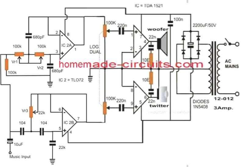 IC 2A is wired as a standard high pass filter.
As the name suggests, the circuit will pass only specified degree of high input frequencies.
The cut off frequency may lie around 3 kHz and can be varied by adjusting VR1 and VR2 or any one of them.
IC 2B is wired in just the opposite configuration i.e.
as a low pass filter and allows only the specified degree of frequencies iver the lower ranges, the cut off frequency being 2.5 kHz.
It will stop all frequencies above this.
The response is adjustable using VR3.
The above suitably equalized audio now is simply fed to an audio amplifier for the required amplifications over the connected loudspeakers.
The channel responsible for producing higher frequencies uses a twitter for better optimization where as the other section which handles the lower frequencies is integrated to a woofer for the relevantly bass output optimization.
IC 2A is wired as a standard high pass filter.
As the name suggests, the circuit will pass only specified degree of high input frequencies.
The cut off frequency may lie around 3 kHz and can be varied by adjusting VR1 and VR2 or any one of them.
IC 2B is wired in just the opposite configuration i.e.
as a low pass filter and allows only the specified degree of frequencies iver the lower ranges, the cut off frequency being 2.5 kHz.
It will stop all frequencies above this.
The response is adjustable using VR3.
The above suitably equalized audio now is simply fed to an audio amplifier for the required amplifications over the connected loudspeakers.
The channel responsible for producing higher frequencies uses a twitter for better optimization where as the other section which handles the lower frequencies is integrated to a woofer for the relevantly bass output optimization.
 Looking the shown circuit above, the design is a typical tone controller circuit, having discrete bass and treble controls.
The first section incorporates a transistor which solely becomes responsible for the required frequency dimensioning functions.
The relevant pots are used for getting the desired bass and treble enhancement effects from the circuit.
Looking the shown circuit above, the design is a typical tone controller circuit, having discrete bass and treble controls.
The first section incorporates a transistor which solely becomes responsible for the required frequency dimensioning functions.
The relevant pots are used for getting the desired bass and treble enhancement effects from the circuit.
 A couple of modules discussed in the above section will need to built and connected to the shown stereo amplifier circuit forcompletingthe proposed home theater circuit design.
 Interesting Feedback from Mr.
Henry Bowman
Swag, IˇŻve been analyzing the three stages of the 4049 schematic and itˇŻs much simpler than I first realized.
The only sections that provide the actual fire is the last two inverters in each chip.
I can utilize one chip to make the machine gun sound.
Using two sets of two inverters each, and making two identical output sounds and delaying one just a few microseconds should make it sound realistic.
I donˇŻt want to hear three different machine gun sounds as it is currently designed.
IˇŻm still using the 4069 chips, which have the same pin configuration as the 74LS04.
See the description below:
CD 4049 machine gun sound operation: On the schematic, In 4049 IC#1, N1 and N2 gates provide the first oscillator section.
Output timing is due to values of R1, R2 and C1. The output at pin 4 is high for about 3 seconds, then goes low for about 4 seconds.
When the output goes low it triggers the next oscillator (N3 & N4) to began oscillation.
Pin 10 on N4 goes low four times during the time that pin 4 on N2 is low.
Each time N2's pin 10 goes low, it triggers the actual machine gun fire that is developed by N5, N6, R5, R6, P1 and C3. N6 pin 15 provides the pulsed output to simulate fire.
P1 adjusts the rate of output (fire) pulses.
The second chip has the same principal as the first one, but some resistance changes which allow longer timing intervals between gun fire bursts .
The same applies to the third chip, with output bursts different from Chip 1 & 2. The rate of output pulses on Chip 3 pin 15 is fixed and non-adjustable.
Pin 15 on each of the three chip's output have different size resistors, ie, 12K, 39K and 120K.
Each pin 15ˇŻs output will have different levels of pulses.
When powered up and connected to an amplifier, it gives the sound effects that there are three machine guns firing, one after the other, from near and distant locations.
Best Wishes,
Henry
More Updates from Mr.
Henry:
The following email information was sent to me by Mr.
Henry Bowman regarding the improvements he made in the above design, allowing the circuit to become better, smaller and simpler.
Here's a technical description and the schematic of the modifications:
Interesting Feedback from Mr.
Henry Bowman
Swag, IˇŻve been analyzing the three stages of the 4049 schematic and itˇŻs much simpler than I first realized.
The only sections that provide the actual fire is the last two inverters in each chip.
I can utilize one chip to make the machine gun sound.
Using two sets of two inverters each, and making two identical output sounds and delaying one just a few microseconds should make it sound realistic.
I donˇŻt want to hear three different machine gun sounds as it is currently designed.
IˇŻm still using the 4069 chips, which have the same pin configuration as the 74LS04.
See the description below:
CD 4049 machine gun sound operation: On the schematic, In 4049 IC#1, N1 and N2 gates provide the first oscillator section.
Output timing is due to values of R1, R2 and C1. The output at pin 4 is high for about 3 seconds, then goes low for about 4 seconds.
When the output goes low it triggers the next oscillator (N3 & N4) to began oscillation.
Pin 10 on N4 goes low four times during the time that pin 4 on N2 is low.
Each time N2's pin 10 goes low, it triggers the actual machine gun fire that is developed by N5, N6, R5, R6, P1 and C3. N6 pin 15 provides the pulsed output to simulate fire.
P1 adjusts the rate of output (fire) pulses.
The second chip has the same principal as the first one, but some resistance changes which allow longer timing intervals between gun fire bursts .
The same applies to the third chip, with output bursts different from Chip 1 & 2. The rate of output pulses on Chip 3 pin 15 is fixed and non-adjustable.
Pin 15 on each of the three chip's output have different size resistors, ie, 12K, 39K and 120K.
Each pin 15ˇŻs output will have different levels of pulses.
When powered up and connected to an amplifier, it gives the sound effects that there are three machine guns firing, one after the other, from near and distant locations.
Best Wishes,
Henry
More Updates from Mr.
Henry:
The following email information was sent to me by Mr.
Henry Bowman regarding the improvements he made in the above design, allowing the circuit to become better, smaller and simpler.
Here's a technical description and the schematic of the modifications:
 "I eliminated two of the chips and only used one 4069. The 4069 is a 14 pin chip, so itˇŻs different than your schematic of the 4049. IˇŻve attached a scribbled schematic to show my modification.
The first oscillator is inverters A & B and the second oscillator is inverters C & D.The inputs of both oscillators are held high by the normally closed push button contacts through a 2K resistor and the two diodes.
Once the push button is pressed, the positive potential is removed and both oscillators start pulsing.
Both oscillators should be adjusted as close as possible to the same pulse rate, using a logic probe or oscilloscope.
When connected to a amp and speaker, tweak one of the 1 meg potentiometers to create a slight delay for a more realistic sound.
Shielded cable should be used from the circuit board to the amp input to reduce hum."
Henry
"I eliminated two of the chips and only used one 4069. The 4069 is a 14 pin chip, so itˇŻs different than your schematic of the 4049. IˇŻve attached a scribbled schematic to show my modification.
The first oscillator is inverters A & B and the second oscillator is inverters C & D.The inputs of both oscillators are held high by the normally closed push button contacts through a 2K resistor and the two diodes.
Once the push button is pressed, the positive potential is removed and both oscillators start pulsing.
Both oscillators should be adjusted as close as possible to the same pulse rate, using a logic probe or oscilloscope.
When connected to a amp and speaker, tweak one of the 1 meg potentiometers to create a slight delay for a more realistic sound.
Shielded cable should be used from the circuit board to the amp input to reduce hum."
Henry
 The following video clip shows the Test Result of the above simplified machine gun sound generatorcircuit through an amplifier (Courtesy: Mr Henry Bowman)
Kindly bear the background Hum sound picked up the amplifier
The following video clip shows the Test Result of the above simplified machine gun sound generatorcircuit through an amplifier (Courtesy: Mr Henry Bowman)
Kindly bear the background Hum sound picked up the amplifier
 This sound generator chip can generate bird chirps, freight train, race track engine, siren, phasor gun, organ (with more push buttons),jungle sounds, wind sounds, etc.
It contains three oscillators being SLF (super low frequency), VCO (voltage controlled oscillator) and noise oscillator.
You can select any combination of these three.
The sound decay function added a lot of realism to the gun shot sound.
I found an old data sheet (attached) that shows someof the sound applications.I plan on adding more rotary switches with selectable capacitors to make more sounds.
Buyers need to be aware that there are two sizes of this chip.
The SN76477 is the standard large size and the SN76477NF is the smaller size.
The NF size socket would be very difficult to use without a printed circuit board, or an adapter.
I finally received two of the larger SN76477 sound chips and very pleased with the results.
I looked all over the Internet to see if anyone had made a mg sound with this chip and no luck.
What I finally wound up doing was to add a 555 timerchip and placed itˇŻs pulsed output on to the one shot pin 9. I added a spdt switch to select the one shot sound or the constant mg sound.
IˇŻm using push buttons for both sound types.
IˇŻm powering the SN76477 with a 9 volt battery.
This chip has a regulated 5 volt output, so IˇŻm using that voltage to power the 555 IC.
The test points enable me to turn off the connection to the ic pins and use a ohm-meter between each test point andˇ°Gˇ± or ground.
I can set each potentiometer to the desired resistance.
I also added a jack to connect to my 200 watt amp.
I havenˇŻt tried that yet.
I tried to send you a longer video explaining each function, but my Iphone said the video was too large, so I really had to condense it.
IˇŻm working on the revised schematic and will send it soon.
This is the revised schematic of the experimenterˇŻs board, correcting the error on pin 9. A positive pulse can be appliedto pin 9 for one-shot sounds, but operating a switch in parallel to the push button to +5 would inhibit all sounds.I corrected the drawing showing a spdt switch on pin 9 to correct the problem.
This sound generator chip can generate bird chirps, freight train, race track engine, siren, phasor gun, organ (with more push buttons),jungle sounds, wind sounds, etc.
It contains three oscillators being SLF (super low frequency), VCO (voltage controlled oscillator) and noise oscillator.
You can select any combination of these three.
The sound decay function added a lot of realism to the gun shot sound.
I found an old data sheet (attached) that shows someof the sound applications.I plan on adding more rotary switches with selectable capacitors to make more sounds.
Buyers need to be aware that there are two sizes of this chip.
The SN76477 is the standard large size and the SN76477NF is the smaller size.
The NF size socket would be very difficult to use without a printed circuit board, or an adapter.
I finally received two of the larger SN76477 sound chips and very pleased with the results.
I looked all over the Internet to see if anyone had made a mg sound with this chip and no luck.
What I finally wound up doing was to add a 555 timerchip and placed itˇŻs pulsed output on to the one shot pin 9. I added a spdt switch to select the one shot sound or the constant mg sound.
IˇŻm using push buttons for both sound types.
IˇŻm powering the SN76477 with a 9 volt battery.
This chip has a regulated 5 volt output, so IˇŻm using that voltage to power the 555 IC.
The test points enable me to turn off the connection to the ic pins and use a ohm-meter between each test point andˇ°Gˇ± or ground.
I can set each potentiometer to the desired resistance.
I also added a jack to connect to my 200 watt amp.
I havenˇŻt tried that yet.
I tried to send you a longer video explaining each function, but my Iphone said the video was too large, so I really had to condense it.
IˇŻm working on the revised schematic and will send it soon.
This is the revised schematic of the experimenterˇŻs board, correcting the error on pin 9. A positive pulse can be appliedto pin 9 for one-shot sounds, but operating a switch in parallel to the push button to +5 would inhibit all sounds.I corrected the drawing showing a spdt switch on pin 9 to correct the problem.
 I will eventually add rotary switches to select various capacitors and be able to create more sounds.
Also need to add three spst switches on pins 25,26 and 27 to combine the sound oscillators.
I will eventually add rotary switches to select various capacitors and be able to create more sounds.
Also need to add three spst switches on pins 25,26 and 27 to combine the sound oscillators.
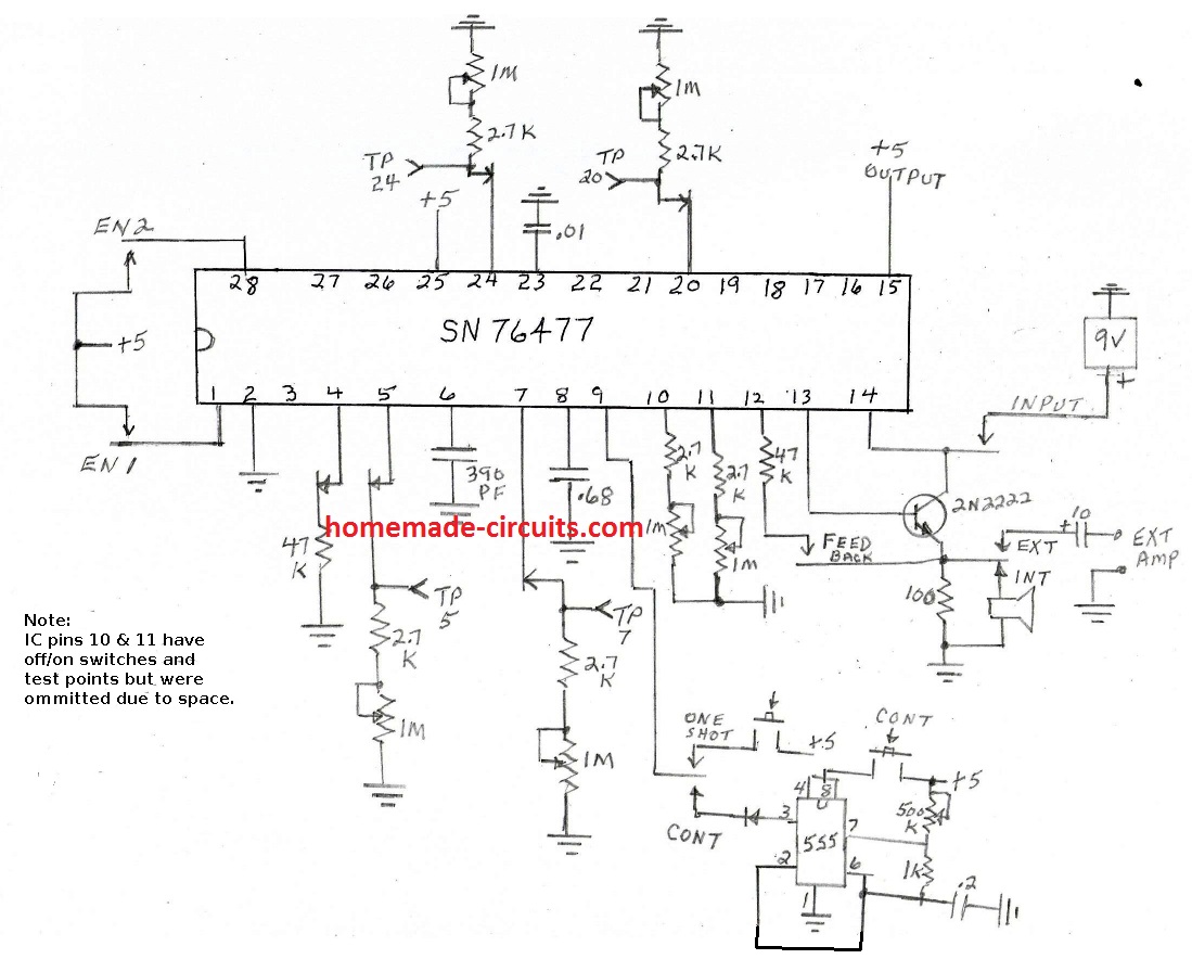
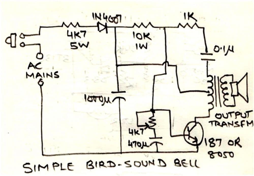
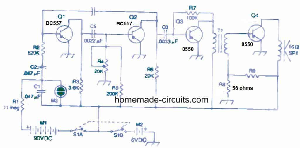
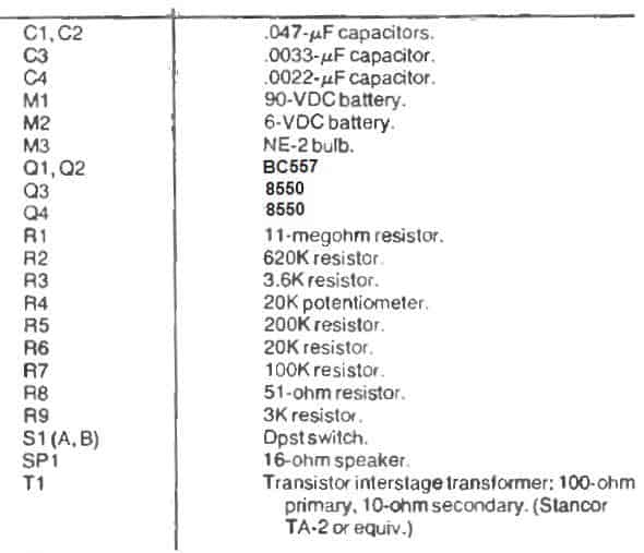 T1 can be any standard audio output transformer as shown below:
 For so long as the counter remains activated, a logic 1 moves across the outputs Q0 to Q9 exactly in accordance with the rhythm with the clock pulses.
The AMV2 oscillator can be expected to imitate the vocal chord of a bird, since it generates an high-frequency note resembling a bird sound.
The AMV3 oscillator becomes responsible for delivering a wide range of frequencies that modulates the AMV2 output.
This is implemented in such a way that the ultimate output simulates exactly a real bird sound, not like the one that you hear from electronic chimes.
The frequency created from the AMV3 oscillator is determined by the value of resistance connected between the capacitor C4 and resistor R4. To be more precise, it is resistor which is switched between R8 and R11.
The switching of these resistors is implemented by CMOS switches ES1 ES4, governed by the many different combinations from the counter outputs.
This particular set up guarantees that the ultimate output is randomly created, and sounds like a real bird and not a monotonously reproducing noise.
The circuit includes a wide variety of rich bird sound customization options.
Remember that it is always possible to alter the resistors R8----R11 values, along with the counter circuit output combinations, with the connections to electronic switches ES1 ES4, in order to customize the bird sound to any desired effect.
For so long as the counter remains activated, a logic 1 moves across the outputs Q0 to Q9 exactly in accordance with the rhythm with the clock pulses.
The AMV2 oscillator can be expected to imitate the vocal chord of a bird, since it generates an high-frequency note resembling a bird sound.
The AMV3 oscillator becomes responsible for delivering a wide range of frequencies that modulates the AMV2 output.
This is implemented in such a way that the ultimate output simulates exactly a real bird sound, not like the one that you hear from electronic chimes.
The frequency created from the AMV3 oscillator is determined by the value of resistance connected between the capacitor C4 and resistor R4. To be more precise, it is resistor which is switched between R8 and R11.
The switching of these resistors is implemented by CMOS switches ES1 ES4, governed by the many different combinations from the counter outputs.
This particular set up guarantees that the ultimate output is randomly created, and sounds like a real bird and not a monotonously reproducing noise.
The circuit includes a wide variety of rich bird sound customization options.
Remember that it is always possible to alter the resistors R8----R11 values, along with the counter circuit output combinations, with the connections to electronic switches ES1 ES4, in order to customize the bird sound to any desired effect.
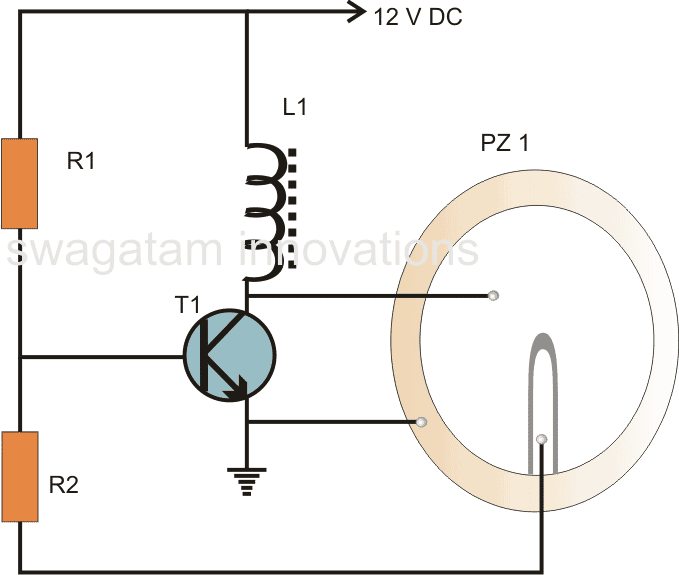
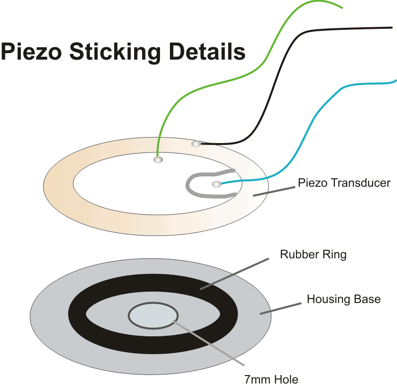
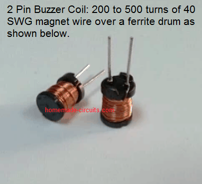 PZ1 = Piezo element, 27mm, three terminal
Rubber ring = 22mm
PZ1 = Piezo element, 27mm, three terminal
Rubber ring = 22mm
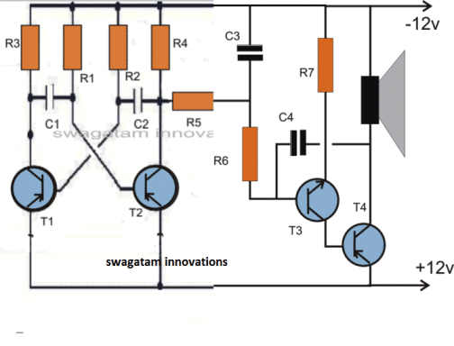
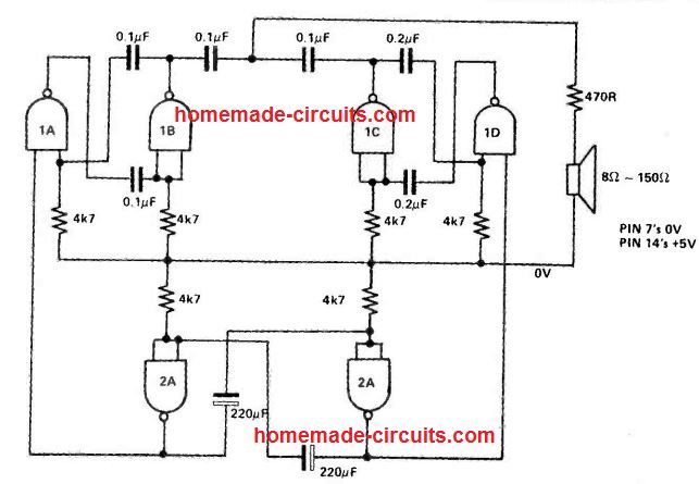 IC 7400 pinout diagram
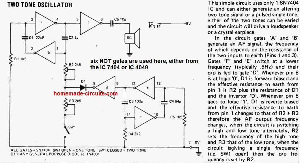
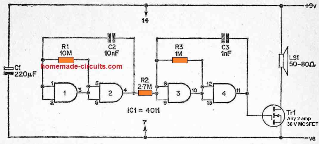 However, R2 only weakly links the modulation astable's output to the tone generator astable's input, and the latter's operating frequency is switched up and down as the modulation oscillator's output shifts from one logic state to another.
As a result, the tone generator's frequency output is altered between roughly 500 Hertz and 1.2 kHz, and it simplydoes not work at its normal operational frequency.
However, R2 only weakly links the modulation astable's output to the tone generator astable's input, and the latter's operating frequency is switched up and down as the modulation oscillator's output shifts from one logic state to another.
As a result, the tone generator's frequency output is altered between roughly 500 Hertz and 1.2 kHz, and it simplydoes not work at its normal operational frequency.
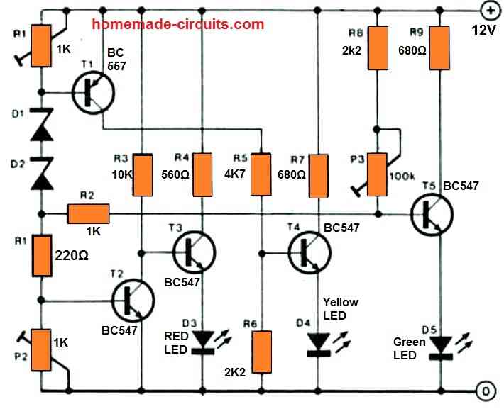
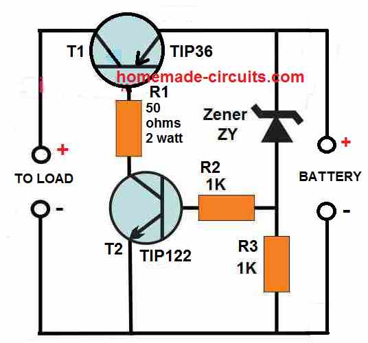 As can be seen, the circuit has a very components, and its working can be understood through the following points:
There are a couple of power transistors coupled with each other where, the base of the TIP36 transistor forms the collector load of the TIP122 transistors.
The base of TIP122 is biased through a resistor/zener diode network, where the zener diode ZY determines the cut off voltage for the TIP122.
The zener diode voltage is selected such that it matches the critical low voltage value of the battery, or any value at which the draining of the battery by the load is required to be stopped.
As long as the battery voltage stays above the zener voltage, or the voltage at which the cut-off needs to happen, the zener diode keeps conducting which in turn keeps the TIP122 in the conducting mode.
With TIP122 conducting the TIP36 gets the required base current, and it also conducts and allows the battery current to pass to the load.
However, the moment the battery voltages reaches or drops below the zener voltage which is also the deep discharge voltage level, causes the zener diode to stop conducting.
When the zener diode stops conducting, the TIP122 base voltage is cut off and it switches OFF.
With TIP122 now switched OFF, the TIP36 is unable to get its base bias current, and it also switches OFF turning off the battery current to the load.
The procedure effectively prevents the battery from further draining and depleting below its deep discharge level.
The indicated load can be any specified load, such as an inverter, a motor, an LED lamp etc.
As can be seen, the circuit has a very components, and its working can be understood through the following points:
There are a couple of power transistors coupled with each other where, the base of the TIP36 transistor forms the collector load of the TIP122 transistors.
The base of TIP122 is biased through a resistor/zener diode network, where the zener diode ZY determines the cut off voltage for the TIP122.
The zener diode voltage is selected such that it matches the critical low voltage value of the battery, or any value at which the draining of the battery by the load is required to be stopped.
As long as the battery voltage stays above the zener voltage, or the voltage at which the cut-off needs to happen, the zener diode keeps conducting which in turn keeps the TIP122 in the conducting mode.
With TIP122 conducting the TIP36 gets the required base current, and it also conducts and allows the battery current to pass to the load.
However, the moment the battery voltages reaches or drops below the zener voltage which is also the deep discharge voltage level, causes the zener diode to stop conducting.
When the zener diode stops conducting, the TIP122 base voltage is cut off and it switches OFF.
With TIP122 now switched OFF, the TIP36 is unable to get its base bias current, and it also switches OFF turning off the battery current to the load.
The procedure effectively prevents the battery from further draining and depleting below its deep discharge level.
The indicated load can be any specified load, such as an inverter, a motor, an LED lamp etc.
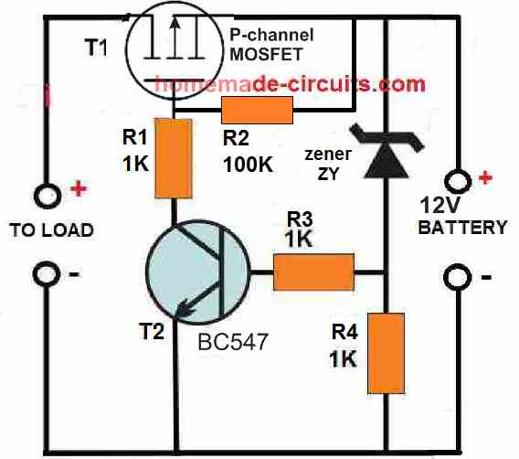 When a MOSFET is used in place of the BJT TIP36, the 50 ohms resistor can be replaced with a 1K resistor or a 10K resistor, and the TIP122 can be replaced with a BC547.
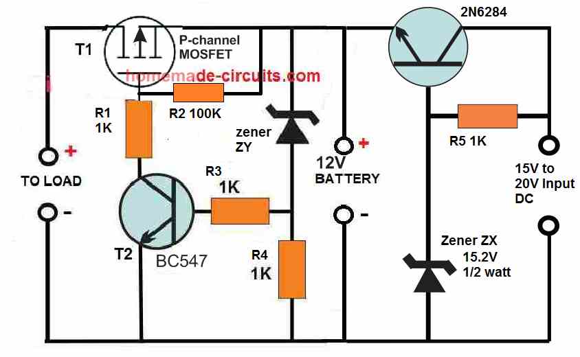 Here we can see a transistor stage on the right side of the design, which is configured as an emitter follower.
The transistor is a 2N6284, which is rated to provide at least 10 amp current to the battery, which means it is able to charge even a 100 Ah battery efficiently.
Since the transistor is a Darlington transistor and configured as an emitter follower, the voltage at its emitter will always lag behind its base voltage by 1 V or 1.2 V.
The zener diode must be cautiously selected so that it compensates the emitter drop of 1.2 V by providing a potential at the base which may be 1.2 V higher than the required emitter voltage.
Since the circuit is designed to charge a 12 V battery, the full charge voltage at the emitter of this transistor must be around 14.1 V.
This implies that the base voltage of the transistor must be 1.2 V higher than the emitter, which amounts to a value of around 15.2 V to 15.3 V.
This is exactly why the zener must be rated at the above specified voltage for generating a constant 14. 1 V at the emitter side and across the connected 12 V battery.
While charging the battery when the battery terminal voltage reaches the 14.1 V value, it reverse biases the emitter of the 2N6284, which shuts down the conduction of the transistor, thereby stopping any further charging of the battery, and the battery is safeguarded from over charging.
The above shown circuit thus implements a 2 in 1 procedure of preventing battery over deep discharge and also over charging through the use a just a few transistors, and still is able to control a battery that may be as big as a 12 V 100 Ah battery.
Here we can see a transistor stage on the right side of the design, which is configured as an emitter follower.
The transistor is a 2N6284, which is rated to provide at least 10 amp current to the battery, which means it is able to charge even a 100 Ah battery efficiently.
Since the transistor is a Darlington transistor and configured as an emitter follower, the voltage at its emitter will always lag behind its base voltage by 1 V or 1.2 V.
The zener diode must be cautiously selected so that it compensates the emitter drop of 1.2 V by providing a potential at the base which may be 1.2 V higher than the required emitter voltage.
Since the circuit is designed to charge a 12 V battery, the full charge voltage at the emitter of this transistor must be around 14.1 V.
This implies that the base voltage of the transistor must be 1.2 V higher than the emitter, which amounts to a value of around 15.2 V to 15.3 V.
This is exactly why the zener must be rated at the above specified voltage for generating a constant 14. 1 V at the emitter side and across the connected 12 V battery.
While charging the battery when the battery terminal voltage reaches the 14.1 V value, it reverse biases the emitter of the 2N6284, which shuts down the conduction of the transistor, thereby stopping any further charging of the battery, and the battery is safeguarded from over charging.
The above shown circuit thus implements a 2 in 1 procedure of preventing battery over deep discharge and also over charging through the use a just a few transistors, and still is able to control a battery that may be as big as a 12 V 100 Ah battery.
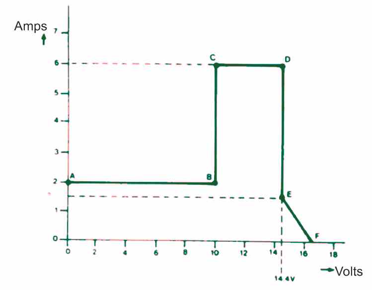 At the initial charging phase (A-B), a controlled low charging current is used, until the battery voltage attains around a 10 V level.
This low current controlled charging is necessary to make sure that the devices of the circuit does not get too much hot initially.
During the next charging stage (C-D), the charging to the battery is done with a 5 hour charging current rate.
This current level can be estimated by dividing the printed Ah spec of the battery by 5. This charging phase can be assumed to be complete when the battery voltage reaches 14.4 V.
At this point, the final charging phase is executed (E-F).
In this phase battery is charged using a significantly scaled-down top-up current, which slowly and automatically drops down to zero when the battery terminal voltage touches the 16.5 V mark.
At the initial charging phase (A-B), a controlled low charging current is used, until the battery voltage attains around a 10 V level.
This low current controlled charging is necessary to make sure that the devices of the circuit does not get too much hot initially.
During the next charging stage (C-D), the charging to the battery is done with a 5 hour charging current rate.
This current level can be estimated by dividing the printed Ah spec of the battery by 5. This charging phase can be assumed to be complete when the battery voltage reaches 14.4 V.
At this point, the final charging phase is executed (E-F).
In this phase battery is charged using a significantly scaled-down top-up current, which slowly and automatically drops down to zero when the battery terminal voltage touches the 16.5 V mark.
 Even at this point the IC1 output continues to be low, which means now the charging current is decided by the presets P1 and P2 both.
In this situation, the setting of P3 causes the voltage at the non-inverting pin of the op amp to increase beyond the zener voltage of D1, then because of the positive feedback arriving from the resistor R4, the IC1 op amp output voltage now switches high, up to a level as determined by the D1 zener voltage, along with the forward voltage drop of diode D2.
With the op amp output turning high, switches OFF the transistor T1, which yet again allows the charge current to be determined by the adjustment of preset P1.
However, contrary to the charging phase A-B, the IC1 output turning high signifies that current would flow by means of the preset P1, and as a result the charging current to the deeply discharged battery would be decreased proportionately.
Because the diode D2 is forward biased, the resistors R2 and R3 will help to progressively minimize the charging current further and further as the battery slowly charges and its voltage gradually increases.
Even at this point the IC1 output continues to be low, which means now the charging current is decided by the presets P1 and P2 both.
In this situation, the setting of P3 causes the voltage at the non-inverting pin of the op amp to increase beyond the zener voltage of D1, then because of the positive feedback arriving from the resistor R4, the IC1 op amp output voltage now switches high, up to a level as determined by the D1 zener voltage, along with the forward voltage drop of diode D2.
With the op amp output turning high, switches OFF the transistor T1, which yet again allows the charge current to be determined by the adjustment of preset P1.
However, contrary to the charging phase A-B, the IC1 output turning high signifies that current would flow by means of the preset P1, and as a result the charging current to the deeply discharged battery would be decreased proportionately.
Because the diode D2 is forward biased, the resistors R2 and R3 will help to progressively minimize the charging current further and further as the battery slowly charges and its voltage gradually increases.


 Fundamentally, the NiCd battery adopts fast charging as opposed to slow charging and employs pulse charge compared to DC charge.
Other types of electrolyte-based chargers favor a rather low discharge feature and mild load currents.
More important, the NiCd battery is robust and works silently while meeting the requirements of tough tasks.
Often, the NiCd performs best in heavily loaded conditions.
Therefore, you should not let the battery sit idly on charging stations or use it only occasionally.
One of the most important practices that must be followed while discharging a NiCd battery is to allow it to complete its periodic cycle.
If you skip this step, large crystals will form on its cell plates which will cause the NiCd to lose its efficiency over time.
The NiCd is famous amongst most rechargeable batteries and these are typically used in two-way radios, emergency medical equipment, and power tools.
Now, the innovation of new batteries with higher energy density and less toxicity is slowly making NiCd less relevant compared to the more novel technologies.
Fundamentally, the NiCd battery adopts fast charging as opposed to slow charging and employs pulse charge compared to DC charge.
Other types of electrolyte-based chargers favor a rather low discharge feature and mild load currents.
More important, the NiCd battery is robust and works silently while meeting the requirements of tough tasks.
Often, the NiCd performs best in heavily loaded conditions.
Therefore, you should not let the battery sit idly on charging stations or use it only occasionally.
One of the most important practices that must be followed while discharging a NiCd battery is to allow it to complete its periodic cycle.
If you skip this step, large crystals will form on its cell plates which will cause the NiCd to lose its efficiency over time.
The NiCd is famous amongst most rechargeable batteries and these are typically used in two-way radios, emergency medical equipment, and power tools.
Now, the innovation of new batteries with higher energy density and less toxicity is slowly making NiCd less relevant compared to the more novel technologies.
 The NiMH battery is fundamentally utilized for storing hydrogen in the form of a nickel-hydrogen battery.
Presently, these types of batteries of commonly found in satellite applications.
They are large and comprise pressurized steel canisters making them reasonably expensive.
During the early developmental days, the NiMH was subjected to reactive metal hydride alloys in the cell environment.
As a result, the expected performance of the battery was not met.
The production of the NiMH was hampered.
Novel hydride alloys were established in the eighties and proven to be stable for use in a cell.
At the end of its decade, the performance was more reliable and improved.
The reason NiMH batteries became successful can be attributed to their compact energy density and the utilization of earth-friendly metals.
In a modern NiMH battery, close to 40% higher energy density is achieved when compared to a NiCd battery.
Although you can go higher with the number, it is not recommended as there are drawbacks.
The NiMH is not as robust as the NiCd.
If you repeatedly use the NiMH with a heavy load or store the battery at high temperatures, the battery life is significantly reduced.
The NiMH will also deplete its charge much faster than the NiCd.
In wireless communication and mobile computing industries, the NiMH is more preferred compared to the NiCd.
Commonly, a buyer is recommended the NiMH battery over NiCd due to its environmental issues including poor disposal procedures.
Industry professionals have a collective say about the NiMH batteryˇŻs colossal improvement over the years.
However, it is still subjected to certain disadvantages which are typical of nickel-based technology, including the NiCd battery.
Moreover, it is agreed that the NiMH is a temporary solution to a more ideal lithium battery technology.
The NiMH battery is fundamentally utilized for storing hydrogen in the form of a nickel-hydrogen battery.
Presently, these types of batteries of commonly found in satellite applications.
They are large and comprise pressurized steel canisters making them reasonably expensive.
During the early developmental days, the NiMH was subjected to reactive metal hydride alloys in the cell environment.
As a result, the expected performance of the battery was not met.
The production of the NiMH was hampered.
Novel hydride alloys were established in the eighties and proven to be stable for use in a cell.
At the end of its decade, the performance was more reliable and improved.
The reason NiMH batteries became successful can be attributed to their compact energy density and the utilization of earth-friendly metals.
In a modern NiMH battery, close to 40% higher energy density is achieved when compared to a NiCd battery.
Although you can go higher with the number, it is not recommended as there are drawbacks.
The NiMH is not as robust as the NiCd.
If you repeatedly use the NiMH with a heavy load or store the battery at high temperatures, the battery life is significantly reduced.
The NiMH will also deplete its charge much faster than the NiCd.
In wireless communication and mobile computing industries, the NiMH is more preferred compared to the NiCd.
Commonly, a buyer is recommended the NiMH battery over NiCd due to its environmental issues including poor disposal procedures.
Industry professionals have a collective say about the NiMH batteryˇŻs colossal improvement over the years.
However, it is still subjected to certain disadvantages which are typical of nickel-based technology, including the NiCd battery.
Moreover, it is agreed that the NiMH is a temporary solution to a more ideal lithium battery technology.
 The lead-acid battery was the first rechargeable battery created by Gaston Plant¨¦ in 1859 for commercial applications.
Presently, the use of lead-acid batteries is spread across various machinery including automobiles, forklifts, and huge uninterruptible power supply systems.
In the seventies, many scientists attempted to design a maintenance-free lead-acid battery and that could work in any position.
The design includes liquid electrolyte which is converted into soaked separators while being in a sealed enclosure.
Then, to permit gas ventilation during charge and discharge, safety valves were incorporated.
Two battery types were developed due to diverse applications.
The first one is a small-sealed lead-acid (SLA) battery or widely known under the brand Gel cell.
The second type is the large valve-regulated lead-acid (VRLA) battery.
In terms of technicalities, they are the same.
However, some engineers may debate that the term ˇ®sealed lead acidˇŻ is misdirection because theoretically, no lead-acid battery is completely sealable.
But since our focus is on portable batteries, we will concentrate only on the SLA.
The lead-acid battery was the first rechargeable battery created by Gaston Plant¨¦ in 1859 for commercial applications.
Presently, the use of lead-acid batteries is spread across various machinery including automobiles, forklifts, and huge uninterruptible power supply systems.
In the seventies, many scientists attempted to design a maintenance-free lead-acid battery and that could work in any position.
The design includes liquid electrolyte which is converted into soaked separators while being in a sealed enclosure.
Then, to permit gas ventilation during charge and discharge, safety valves were incorporated.
Two battery types were developed due to diverse applications.
The first one is a small-sealed lead-acid (SLA) battery or widely known under the brand Gel cell.
The second type is the large valve-regulated lead-acid (VRLA) battery.
In terms of technicalities, they are the same.
However, some engineers may debate that the term ˇ®sealed lead acidˇŻ is misdirection because theoretically, no lead-acid battery is completely sealable.
But since our focus is on portable batteries, we will concentrate only on the SLA.
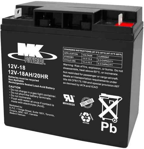 Dissimilar to the flooded lead-acid battery, both SLA and VRLA are developed with faint over-voltage potential to deter the battery from achieving its gas-penetration potential when charging.
Overcharging the battery will result in gassing and water depletion.
So, it is crucial to remember not to charge these batteries to the brim.
Furthermore, the issue of memory is not present with the lead-acid battery.
If you leave the battery on float charge for a long duration, it will not be damaged.
The batteryˇŻs charge holding is one of the best if compared with other rechargeable batteries.
Meanwhile, the NiCd battery self-discharges about 40% of its accumulated energy in just 90 days whereas the SLA self-discharge the same in approximately a year.
Given that the SLA is a cheaper option compared to the NiCd, its functional costs can skyrocket than the latter if full cycles are needed repeatedly.
The SLA prefers slow charging and usually takes around 8 to 16 hours.
Also, it is crucial that the SLA is fully charged when storing.
Nominally, the loss of charge over time also depends on battery chemistries in different conditions.
To avoid SLA batteries from being stressed through tedious discharge, bigger models are preferred.
The SLA can deliver up to 200 ¨C 300 discharge/charge cycles depending on the working temperature and discharge depth.
The short life cycle of the SLA is attributed mainly to grid corrosion of the positive electrode, reduction of the active material, and sulphation of the positive plates.
These alterations are more prominent at heightened operating temperatures.
So, cycling does not deter or undo the trend.
The nominal operating temperature for the SLA and VRLA batteries is 25ˇăC or 77ˇăF.
The ultimate rule is that for every 8ˇăC (15ˇăF) elevation in the temperature, the battery life is halved.
That means a VRLA battery that is intended to last for 10 years at 25ˇăC will only work properly for 5 years if you work the battery at 33ˇăC (95ˇăF).
If you elevate the temperature further, say at 42ˇăC or 107ˇăF, the same battery will only last a little longer than a year.
Dissimilar to the flooded lead-acid battery, both SLA and VRLA are developed with faint over-voltage potential to deter the battery from achieving its gas-penetration potential when charging.
Overcharging the battery will result in gassing and water depletion.
So, it is crucial to remember not to charge these batteries to the brim.
Furthermore, the issue of memory is not present with the lead-acid battery.
If you leave the battery on float charge for a long duration, it will not be damaged.
The batteryˇŻs charge holding is one of the best if compared with other rechargeable batteries.
Meanwhile, the NiCd battery self-discharges about 40% of its accumulated energy in just 90 days whereas the SLA self-discharge the same in approximately a year.
Given that the SLA is a cheaper option compared to the NiCd, its functional costs can skyrocket than the latter if full cycles are needed repeatedly.
The SLA prefers slow charging and usually takes around 8 to 16 hours.
Also, it is crucial that the SLA is fully charged when storing.
Nominally, the loss of charge over time also depends on battery chemistries in different conditions.
To avoid SLA batteries from being stressed through tedious discharge, bigger models are preferred.
The SLA can deliver up to 200 ¨C 300 discharge/charge cycles depending on the working temperature and discharge depth.
The short life cycle of the SLA is attributed mainly to grid corrosion of the positive electrode, reduction of the active material, and sulphation of the positive plates.
These alterations are more prominent at heightened operating temperatures.
So, cycling does not deter or undo the trend.
The nominal operating temperature for the SLA and VRLA batteries is 25ˇăC or 77ˇăF.
The ultimate rule is that for every 8ˇăC (15ˇăF) elevation in the temperature, the battery life is halved.
That means a VRLA battery that is intended to last for 10 years at 25ˇăC will only work properly for 5 years if you work the battery at 33ˇăC (95ˇăF).
If you elevate the temperature further, say at 42ˇăC or 107ˇăF, the same battery will only last a little longer than a year.
 The development of the lithium battery commenced in 1912 under the research of G.N.
Lewis.
However, until the late seventies, the application of the first non-rechargeable lithium batteries was not practiced.
Since lithium is the lightest metal available, it possesses the best electromechanical potential which eventually contributed to the greatest energy density per weight.
Because of safety concerns, further research into rechargeable lithium batteries was stalled in the 1980s.
Scientists were alarmed due to the volatility of lithium metal when charging and so they channeled all research efforts to non-metallic lithium battery which comprise lithium ions instead of the active metal.
The development of the lithium battery commenced in 1912 under the research of G.N.
Lewis.
However, until the late seventies, the application of the first non-rechargeable lithium batteries was not practiced.
Since lithium is the lightest metal available, it possesses the best electromechanical potential which eventually contributed to the greatest energy density per weight.
Because of safety concerns, further research into rechargeable lithium batteries was stalled in the 1980s.
Scientists were alarmed due to the volatility of lithium metal when charging and so they channeled all research efforts to non-metallic lithium battery which comprise lithium ions instead of the active metal.
 The Lithium polymer battery or the Lipo battery is different from other battery models in terms of the type of electrolyte.
The first design which was developed in the 1970s employed the use of dry solid polymer electrolyte.
This chemical compound looks like a plastic film that acts as an insulator but permits the transaction of ions (electrically charged atoms).
The polymer electrolyte substitutes the standard porous separator, which is drenched in the electrolyte.
The dry polymer build presents a simpler construction in terms of manufacturing, durability, safety, and slim geometry.
Moreover, the fire hazard is eliminated due to the absence of liquid or gelled electrolyte.
The designers are free to build the battery as creatively as possible with various forms, shapes, and sizes thanks to the ultra-slim cell thickness which measures only 1 mm.
However, the dry Li-polymer is not a good conductor.
Its internal resistance is too large and unable to channel the current surges which are necessary for modern communications machines and powering hard drives of mobile computing devices.
You can ramp the conductivity by heating the cell to 60ˇăC (140ˇăF), but it is impractical for portable purposes.
The gelled electrolyte was added to ensure a small Li-polymer battery becomes conductive.
A wide collection of Li-polymer batteries used today for handphones are a hybrid type and comprise gelled electrolytes.
The right term for this design is Lithium-Ion Polymer.
For marketing purposes, most battery producers mark their batteries as Li-polymer.
We will only pay attention to the hybrid lithium polymer because it is the only functioning polymer chemistry for portable batteries presently.
The Lithium polymer battery or the Lipo battery is different from other battery models in terms of the type of electrolyte.
The first design which was developed in the 1970s employed the use of dry solid polymer electrolyte.
This chemical compound looks like a plastic film that acts as an insulator but permits the transaction of ions (electrically charged atoms).
The polymer electrolyte substitutes the standard porous separator, which is drenched in the electrolyte.
The dry polymer build presents a simpler construction in terms of manufacturing, durability, safety, and slim geometry.
Moreover, the fire hazard is eliminated due to the absence of liquid or gelled electrolyte.
The designers are free to build the battery as creatively as possible with various forms, shapes, and sizes thanks to the ultra-slim cell thickness which measures only 1 mm.
However, the dry Li-polymer is not a good conductor.
Its internal resistance is too large and unable to channel the current surges which are necessary for modern communications machines and powering hard drives of mobile computing devices.
You can ramp the conductivity by heating the cell to 60ˇăC (140ˇăF), but it is impractical for portable purposes.
The gelled electrolyte was added to ensure a small Li-polymer battery becomes conductive.
A wide collection of Li-polymer batteries used today for handphones are a hybrid type and comprise gelled electrolytes.
The right term for this design is Lithium-Ion Polymer.
For marketing purposes, most battery producers mark their batteries as Li-polymer.
We will only pay attention to the hybrid lithium polymer because it is the only functioning polymer chemistry for portable batteries presently.

 IC1B becomes the main active part of the the astable multivibrator configuration.
Capacitor C1 and resistor R4 which are connected across the feedback path provide a working frequency of 15 kHz roughly.
Diode D1 and resistor R7 make sure that the square wave output operates with a 50:50 duty cycle.
C1 capacitor must be a good quality capacitor with high stability and low temperature coefficient features, a ceramic type capacitor should do the job well.
The dode D1 should be rated with a temperature characteristics so that the output square wave is maintained correctly all the time regardless of the output load conditions and circuit heating.
Transistors T2 and T3 gets switched alternately through the square waves generated by the IC1B.
When T3 is in the switched ON period, capacitor C3 charges up to 12 V by means of D2. Next, while the T3 goes into the switched OFF period, causes T2 to turn ON, which enables the negative terminal of C3 to be instantly linked with the +12 V supply.
However, in this situation the charge stored inside in C3 is unable to change immediately, therefore as soon as the C3 negative terminal gets linked with the high 12 V potential, it becomes necessary for its positive terminal to also step up.
The situation causes the C3 positive terminal to get ˇ®boosted upˇŻ to approximately two times the supply voltage.
In real life operation , due to the losses occurring through the diodes and transistors essentially mean that the output cannot be exactly two times the supply input level, rather will be a slightly below the expected 2X level.
Schottky diodes are employed in the circuit to ensure that the forward voltage drop is kept to the minimum.
D3 is used for rectifying the voltage and C4 is configured to store the rectified output from the diode.
Make sure to use very high quality capacitor for C3 since it will be solely responsible for delivering the entire output current to the load.
The regulation for the output voltage is executed by op-amp IC1A.
The potential divider created by the resistors R14 and R12 detects the T4 collector voltage and then IC1A compares it with the reference voltage generated from the network comprising of the parts R6, R9 and zener diode D4.
The level of the stepped up 19 V output can be fixed by adjusting the value of R14. A 15 k value for R14 will provide an approximate output voltage of 19 V.
The ripple voltage content of the 19 V output at full load will be as shown in the next figure.
IC1B becomes the main active part of the the astable multivibrator configuration.
Capacitor C1 and resistor R4 which are connected across the feedback path provide a working frequency of 15 kHz roughly.
Diode D1 and resistor R7 make sure that the square wave output operates with a 50:50 duty cycle.
C1 capacitor must be a good quality capacitor with high stability and low temperature coefficient features, a ceramic type capacitor should do the job well.
The dode D1 should be rated with a temperature characteristics so that the output square wave is maintained correctly all the time regardless of the output load conditions and circuit heating.
Transistors T2 and T3 gets switched alternately through the square waves generated by the IC1B.
When T3 is in the switched ON period, capacitor C3 charges up to 12 V by means of D2. Next, while the T3 goes into the switched OFF period, causes T2 to turn ON, which enables the negative terminal of C3 to be instantly linked with the +12 V supply.
However, in this situation the charge stored inside in C3 is unable to change immediately, therefore as soon as the C3 negative terminal gets linked with the high 12 V potential, it becomes necessary for its positive terminal to also step up.
The situation causes the C3 positive terminal to get ˇ®boosted upˇŻ to approximately two times the supply voltage.
In real life operation , due to the losses occurring through the diodes and transistors essentially mean that the output cannot be exactly two times the supply input level, rather will be a slightly below the expected 2X level.
Schottky diodes are employed in the circuit to ensure that the forward voltage drop is kept to the minimum.
D3 is used for rectifying the voltage and C4 is configured to store the rectified output from the diode.
Make sure to use very high quality capacitor for C3 since it will be solely responsible for delivering the entire output current to the load.
The regulation for the output voltage is executed by op-amp IC1A.
The potential divider created by the resistors R14 and R12 detects the T4 collector voltage and then IC1A compares it with the reference voltage generated from the network comprising of the parts R6, R9 and zener diode D4.
The level of the stepped up 19 V output can be fixed by adjusting the value of R14. A 15 k value for R14 will provide an approximate output voltage of 19 V.
The ripple voltage content of the 19 V output at full load will be as shown in the next figure.
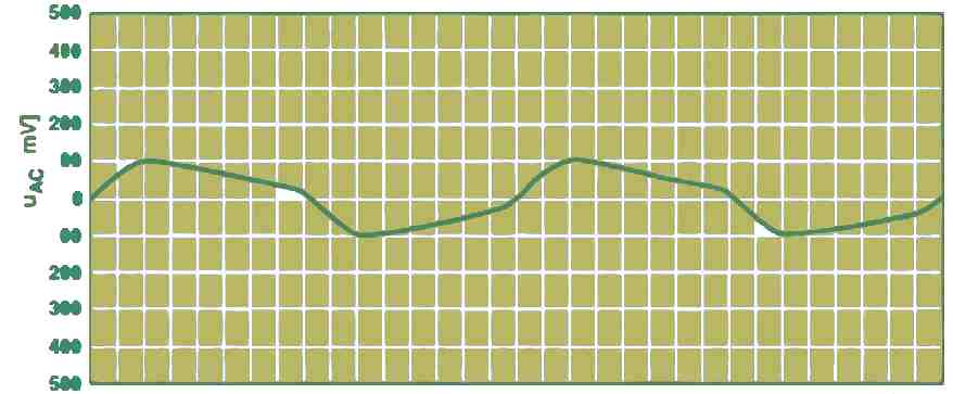 If the capacitor value C6 is increased, will ensure that the reference voltage goes up at a very slow rate when power is first switched ON.
This feature can provide this 12 V to 19 v converter circuit a nice soft-start or slow-start characteristic.
This switch-on delay can be verified by looking at the LED D6.
If the capacitor value C6 is increased, will ensure that the reference voltage goes up at a very slow rate when power is first switched ON.
This feature can provide this 12 V to 19 v converter circuit a nice soft-start or slow-start characteristic.
This switch-on delay can be verified by looking at the LED D6.

 500 AMP SCR Image
Since SCRs are available up to even 1000 amps range, the battery charger does not have any range limitation, and almost any battery with highest levels could be used with this charger circuit.
Being completely solid state by nature, the SCR battery charger does not have any wear and tear compared to relay based battery chargers, whose contacts continuously go though sparking and degradation until the relay is ultimately worn out and malfunctioning.
But no such issues with this SCR systems, as these devices are very long lasting and can be used infinitely.
500 AMP SCR Image
Since SCRs are available up to even 1000 amps range, the battery charger does not have any range limitation, and almost any battery with highest levels could be used with this charger circuit.
Being completely solid state by nature, the SCR battery charger does not have any wear and tear compared to relay based battery chargers, whose contacts continuously go though sparking and degradation until the relay is ultimately worn out and malfunctioning.
But no such issues with this SCR systems, as these devices are very long lasting and can be used infinitely.
 SCR1 = 10 to 20 amp, SCR2 = C106, R2 and R3 must be 10 watt rated, D1, D2 = 6A4 and D3 = 1N4007, ZD1 = 6V 1 watt zener
A center tap transformer is used as the power source for charging the battery.
It must be suitably rated to handle the battery charging current.
Preferably for lead acid battery the current capacity of the transformer must be 10 to 8 times less than the battery Ah value.
So for a 100 Ah battery, the transformer must be 12 amps, for 500 Ah battery this can be rated at 60 amps and so on.
The stepped down AC from the battery is full wave rectified using diodes D1, D2.
You can see no filter capacitor used after the diodes for two reasons:
If clean DC is used then the SCR1 will get permanently latched, and cannot be cut-off by removing its gate bias
Battery usually do not need smooth DC to charge, it is fine as long as the the charge current is a DC, with constant current and full charge cut-off.
When power is switched ON, the capacitor C1 ensures that it grounds the SCR2 gate and inhibits from conducting, regardless of the battery voltage.
With SCR2 switch OFF, the Dc from the D1/D2 easily reaches the SCR1 gate, and triggers it ON.
SCR1 now begins supplying the charging voltage and current to the connected battery across its cathode and ground.
The entire supply voltage from the transformer now drops and settles down to the battery discharge level.
This happen because the transformer current is 10 times less than the battery Ah value, which forces it to drop to the battery discharge level.
So if the initial discharged level of the battery was 11 V, the DC from the transformer would also drop to 11V and slowly rise as the battery is gradually charged by the SCR1
A resistive divider network built using R1/R5, now begins monitoring the battery voltage.
C1 now acts like a filter capacitor for stabilizing the gate input to the SCR2 via the above resistive divider.
Initially the R1 preset is set such that the SCR2 just switches ON when the connected battery reaches its full charge level.
For example, for a 12 V battery, R1 can be set such that the ZD1 zener at the gate of SCR2 just begins conducting when the battery voltage has reached around 14.3 V, so that SCR2 is able to fire at around 14,3 V, and cut off SCR1 gate supply.
Therefore, as the battery charges, and reaches the predetermined value, the voltage across C1 is sufficiently high to allow the zener ZD1 to conduct.
This in turn, causes the SCR2 to fire, which pulls the gate voltage of SCR1 to ground inhibiting it gate bias.
The SCR2 goes into a permanent latching mode since its gate has a filter capacitor in the form of C1, so it is able to get the required pure DC for the latching purpose.
The above situation causes the SCR1 to shut off, and cut-off the charging current to the battery.
After this, due to absence of a charging voltage the battery voltage starts dropping slowly until it reaches the stable state of charge (SoC), which may be around 12.6 V to 12.8 V for a fully charged 12 V battery.
Since SCR2 is latched, the dropping of the battery voltage to its SoC level does not cause any difference to the shut down situation of the charger.
The SCR charger circuit remains in this condition infinitely until, either the battery is removed or the input power is turned OFF and ON again for a new cycle.
SCR1 = 10 to 20 amp, SCR2 = C106, R2 and R3 must be 10 watt rated, D1, D2 = 6A4 and D3 = 1N4007, ZD1 = 6V 1 watt zener
A center tap transformer is used as the power source for charging the battery.
It must be suitably rated to handle the battery charging current.
Preferably for lead acid battery the current capacity of the transformer must be 10 to 8 times less than the battery Ah value.
So for a 100 Ah battery, the transformer must be 12 amps, for 500 Ah battery this can be rated at 60 amps and so on.
The stepped down AC from the battery is full wave rectified using diodes D1, D2.
You can see no filter capacitor used after the diodes for two reasons:
If clean DC is used then the SCR1 will get permanently latched, and cannot be cut-off by removing its gate bias
Battery usually do not need smooth DC to charge, it is fine as long as the the charge current is a DC, with constant current and full charge cut-off.
When power is switched ON, the capacitor C1 ensures that it grounds the SCR2 gate and inhibits from conducting, regardless of the battery voltage.
With SCR2 switch OFF, the Dc from the D1/D2 easily reaches the SCR1 gate, and triggers it ON.
SCR1 now begins supplying the charging voltage and current to the connected battery across its cathode and ground.
The entire supply voltage from the transformer now drops and settles down to the battery discharge level.
This happen because the transformer current is 10 times less than the battery Ah value, which forces it to drop to the battery discharge level.
So if the initial discharged level of the battery was 11 V, the DC from the transformer would also drop to 11V and slowly rise as the battery is gradually charged by the SCR1
A resistive divider network built using R1/R5, now begins monitoring the battery voltage.
C1 now acts like a filter capacitor for stabilizing the gate input to the SCR2 via the above resistive divider.
Initially the R1 preset is set such that the SCR2 just switches ON when the connected battery reaches its full charge level.
For example, for a 12 V battery, R1 can be set such that the ZD1 zener at the gate of SCR2 just begins conducting when the battery voltage has reached around 14.3 V, so that SCR2 is able to fire at around 14,3 V, and cut off SCR1 gate supply.
Therefore, as the battery charges, and reaches the predetermined value, the voltage across C1 is sufficiently high to allow the zener ZD1 to conduct.
This in turn, causes the SCR2 to fire, which pulls the gate voltage of SCR1 to ground inhibiting it gate bias.
The SCR2 goes into a permanent latching mode since its gate has a filter capacitor in the form of C1, so it is able to get the required pure DC for the latching purpose.
The above situation causes the SCR1 to shut off, and cut-off the charging current to the battery.
After this, due to absence of a charging voltage the battery voltage starts dropping slowly until it reaches the stable state of charge (SoC), which may be around 12.6 V to 12.8 V for a fully charged 12 V battery.
Since SCR2 is latched, the dropping of the battery voltage to its SoC level does not cause any difference to the shut down situation of the charger.
The SCR charger circuit remains in this condition infinitely until, either the battery is removed or the input power is turned OFF and ON again for a new cycle.
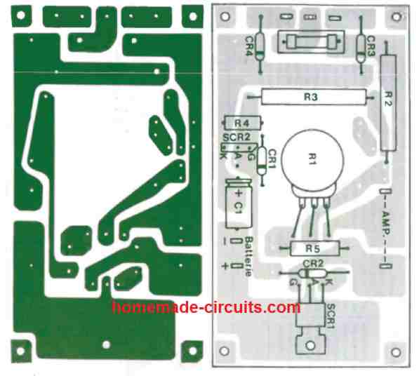
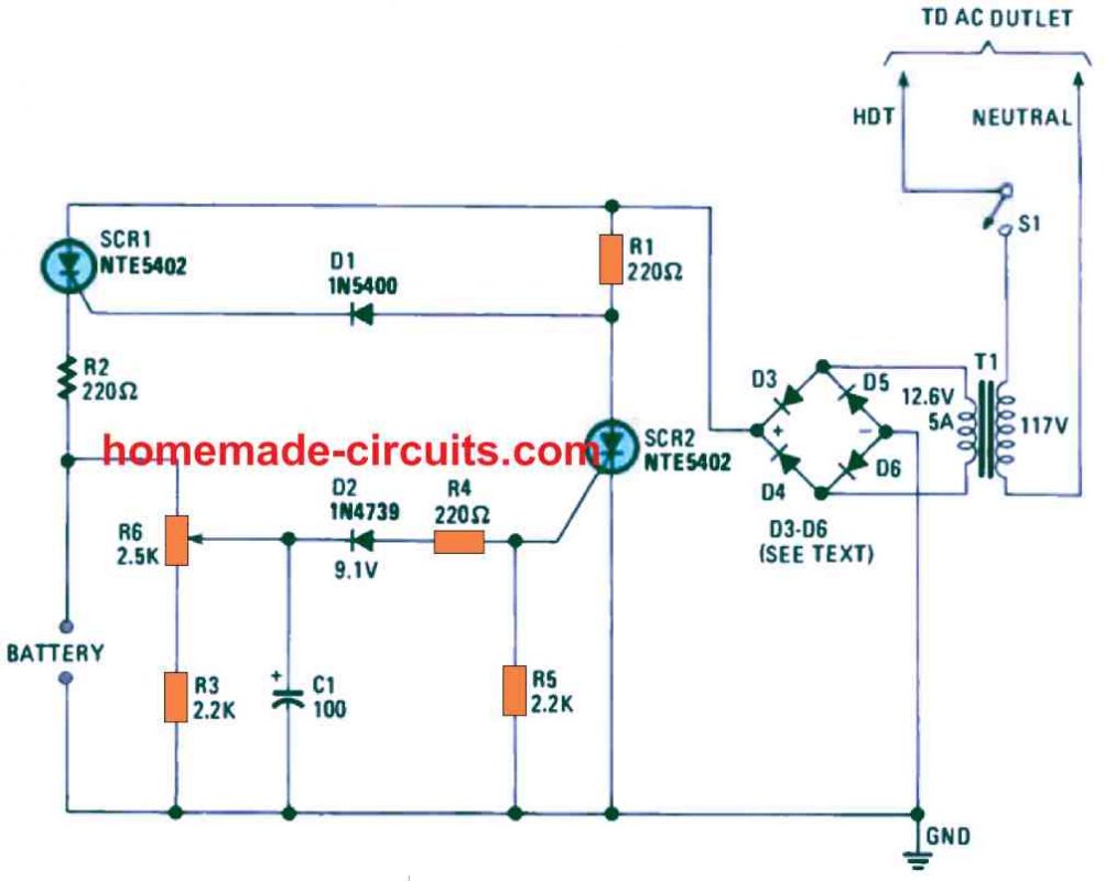 During the time the battery gets the maximum charge current, resistor R1 and diode D1 switches ON SCR1 so that it is able to deliver the the full current to the battery.
You can find the voltage over R6 and R3 is fairly low, which causes D2 to stop conducting; turning OFF the SCR2 off.
The voltage from which SCR2 is able to trigger ON is defined by potentiometer R6. When D2 begins transferring gate current to SCR2, it turns on, causing diode D1 to become reverse biased.
The voltage for D1, which is pulled by means of R1, declines to practically zero.
This prevents SCR1 from activating.
The results in a sluggish rate of current and the triggering angle of SCR1 is minimized as the battery terminal voltage goes up.
You can experiment with a limiting resistor, to alter the rate of charging
During the time the battery gets the maximum charge current, resistor R1 and diode D1 switches ON SCR1 so that it is able to deliver the the full current to the battery.
You can find the voltage over R6 and R3 is fairly low, which causes D2 to stop conducting; turning OFF the SCR2 off.
The voltage from which SCR2 is able to trigger ON is defined by potentiometer R6. When D2 begins transferring gate current to SCR2, it turns on, causing diode D1 to become reverse biased.
The voltage for D1, which is pulled by means of R1, declines to practically zero.
This prevents SCR1 from activating.
The results in a sluggish rate of current and the triggering angle of SCR1 is minimized as the battery terminal voltage goes up.
You can experiment with a limiting resistor, to alter the rate of charging
 Additionally, this bears another advantage over the conventional cells as aluminium is better at improving heat conduction from the cell.
One more innovative design is the casing which forms the positive terminal of the cell.
It is built with a thin layer of ferromagnetic material that forms the real contacts.
Additionally, this bears another advantage over the conventional cells as aluminium is better at improving heat conduction from the cell.
One more innovative design is the casing which forms the positive terminal of the cell.
It is built with a thin layer of ferromagnetic material that forms the real contacts.
 Surprisingly, the difference in the final temperature is low (47ˇăC against 49ˇăC).
This is because the internal resistance of the cells is dependent on the temperature.
That means when the cells are cold (low temperature), substantially more power is dissipated internally.
The next examination was related to the discharge current where it increased to 15 C (34.5 A), the cells presented more than their minimum capacity as the temperature escalated to 53ˇăC from 23ˇăC.
Surprisingly, the difference in the final temperature is low (47ˇăC against 49ˇăC).
This is because the internal resistance of the cells is dependent on the temperature.
That means when the cells are cold (low temperature), substantially more power is dissipated internally.
The next examination was related to the discharge current where it increased to 15 C (34.5 A), the cells presented more than their minimum capacity as the temperature escalated to 53ˇăC from 23ˇăC.
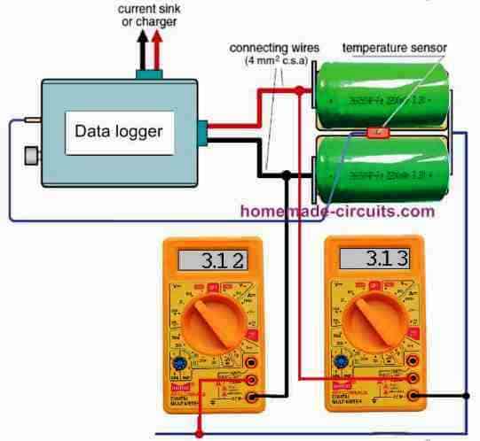 The combination of resistances including the 1 m¦¸ shunt resistor, the built-in resistance of the 100 A current sink and its associates (cable resistances and contact resistances in the MPX connector).
The extreme low resistance prevented the discharge of a single charge from going more than 65 A.
Therefore, we attempted delegating the high current measurements using two cells in series like before.
Due to that, we could measure the voltage between the cells using a multimeter.
The current sink in this experiment may have been overloaded because of the cellˇŻs rated current of 120 A.
By limiting the extent of our evaluation, we monitored the temperature elevates at 15 C discharge.
This showed that it is not fitting to test the cells all at once at their rated continuous discharge rate of 30 C (70 A).
There is substantial evidence that a cell surface temperature of 65ˇăC during discharge is the upper limit for safety.
So, we constructed the resulting discharge schedule.
Firstly, at 69 A (30 C) the cells are discharged for 16 seconds.
Then, it was followed by alternating ˇ®recoveryˇŻ intervals of 11.5 A (5 C) for half a minute.
After that, there were 10-second pulses at 69 A.
Finally, when either the minimum discharge voltage or maximum permissible temperature was achieved, the discharge was operation was ended.
Figure 4 depicts the results that were obtained.
The combination of resistances including the 1 m¦¸ shunt resistor, the built-in resistance of the 100 A current sink and its associates (cable resistances and contact resistances in the MPX connector).
The extreme low resistance prevented the discharge of a single charge from going more than 65 A.
Therefore, we attempted delegating the high current measurements using two cells in series like before.
Due to that, we could measure the voltage between the cells using a multimeter.
The current sink in this experiment may have been overloaded because of the cellˇŻs rated current of 120 A.
By limiting the extent of our evaluation, we monitored the temperature elevates at 15 C discharge.
This showed that it is not fitting to test the cells all at once at their rated continuous discharge rate of 30 C (70 A).
There is substantial evidence that a cell surface temperature of 65ˇăC during discharge is the upper limit for safety.
So, we constructed the resulting discharge schedule.
Firstly, at 69 A (30 C) the cells are discharged for 16 seconds.
Then, it was followed by alternating ˇ®recoveryˇŻ intervals of 11.5 A (5 C) for half a minute.
After that, there were 10-second pulses at 69 A.
Finally, when either the minimum discharge voltage or maximum permissible temperature was achieved, the discharge was operation was ended.
Figure 4 depicts the results that were obtained.
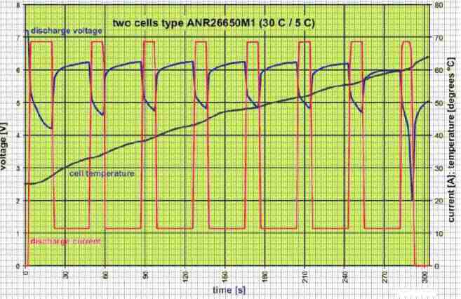 Throughout the high load intervals, the terminal voltage dropped quickly, representing that the lithium ions inside the cells have restricted and slow movement.
Still, the cell improves swiftly during the low-load intervals.
Though the voltage slowly falls as the cell is discharged, you may find considerably less accurate voltage drops by the higher loads, as the cell temperature increases.
This validates how the temperature is dependent on the internal resistance of the cell.
We recorded an internal resistance to DC to be about 11 m¦¸ (datasheet presents 10 m¦¸) when the cell is half discharged.
When the cell had fully discharged, the temperature had risen to 63ˇăC, which exposes it to safety risks.
This is because there is no additional cooling for the cells thus, we stopped from proceeding to testing with longer high-load pulses.
The battery gave an output of 2320 mAh in this test which was greater than the nominal capacity.
With a maximum difference between the cell voltages at 10 mV, the matching between them was outstanding throughout the test.
The discharge at full load was halted when the terminal voltage achieved 1 V per cell.
A minute later, we saw a recovery of 2.74 V open circuit voltage over each of the cells.
Throughout the high load intervals, the terminal voltage dropped quickly, representing that the lithium ions inside the cells have restricted and slow movement.
Still, the cell improves swiftly during the low-load intervals.
Though the voltage slowly falls as the cell is discharged, you may find considerably less accurate voltage drops by the higher loads, as the cell temperature increases.
This validates how the temperature is dependent on the internal resistance of the cell.
We recorded an internal resistance to DC to be about 11 m¦¸ (datasheet presents 10 m¦¸) when the cell is half discharged.
When the cell had fully discharged, the temperature had risen to 63ˇăC, which exposes it to safety risks.
This is because there is no additional cooling for the cells thus, we stopped from proceeding to testing with longer high-load pulses.
The battery gave an output of 2320 mAh in this test which was greater than the nominal capacity.
With a maximum difference between the cell voltages at 10 mV, the matching between them was outstanding throughout the test.
The discharge at full load was halted when the terminal voltage achieved 1 V per cell.
A minute later, we saw a recovery of 2.74 V open circuit voltage over each of the cells.
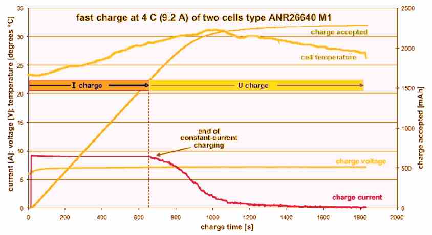 When using lead-acid batteries, we can only set the initial charging current due to the maximum and limited voltage delivered by the charger.
Also, the charging current can only be set after the cell voltage had risen to a point where the charge current starts reducing (constant current/constant voltage charging).
In our experiment with LiFePO4, this happens after 10 minutes where the duration is reduced by the effect of the shunt in the meter.
We know the cell is charged to 97% or more of its nominal capacity after 20 minutes had elapsed.
Furthermore, the charge current at this stage has dropped to 0.5 A.
As a result, a ˇ®fullˇŻ state of the cells will be reported by a fast charger.
Throughout the fast charging process, the cell voltages sometimes moved a little bit from each other, but not beyond 20 mV.
But for the overall of the process, the cells finished charging at the same time.
When experience fast charging, the cells tend to warm up quite a bit, with the temperature somewhat lagging the charge current.
This can be attributed to losses in the internal resistance of the cells.
It is fundamental to follow safety precautions when charging the LiFePO4 and not beyond its suggested charging voltage of 3.6 V.
We tried to sneak past a little and attempted to ˇ®overchargeˇŻ the cells with a terminal voltage of 7.8 V (3.9 V per cell).
It is not at all recommended to repeat this at home.
Although there was no strange behavior such as smoking or leaking and the cell voltages were also almost equal, but the overall outcome did not appear to be too beneficial.
The 3 C discharge supplied an additional 100 mAh and the mean discharge voltage was relatively higher.
What we mean to say is overcharging causes a small upheave in energy density from 103.6 Wh/kg to 104.6 Wh/kg.
However, it is not worth it to endure the risks and possibly subject the life of the cells to permanent damage.
When using lead-acid batteries, we can only set the initial charging current due to the maximum and limited voltage delivered by the charger.
Also, the charging current can only be set after the cell voltage had risen to a point where the charge current starts reducing (constant current/constant voltage charging).
In our experiment with LiFePO4, this happens after 10 minutes where the duration is reduced by the effect of the shunt in the meter.
We know the cell is charged to 97% or more of its nominal capacity after 20 minutes had elapsed.
Furthermore, the charge current at this stage has dropped to 0.5 A.
As a result, a ˇ®fullˇŻ state of the cells will be reported by a fast charger.
Throughout the fast charging process, the cell voltages sometimes moved a little bit from each other, but not beyond 20 mV.
But for the overall of the process, the cells finished charging at the same time.
When experience fast charging, the cells tend to warm up quite a bit, with the temperature somewhat lagging the charge current.
This can be attributed to losses in the internal resistance of the cells.
It is fundamental to follow safety precautions when charging the LiFePO4 and not beyond its suggested charging voltage of 3.6 V.
We tried to sneak past a little and attempted to ˇ®overchargeˇŻ the cells with a terminal voltage of 7.8 V (3.9 V per cell).
It is not at all recommended to repeat this at home.
Although there was no strange behavior such as smoking or leaking and the cell voltages were also almost equal, but the overall outcome did not appear to be too beneficial.
The 3 C discharge supplied an additional 100 mAh and the mean discharge voltage was relatively higher.
What we mean to say is overcharging causes a small upheave in energy density from 103.6 Wh/kg to 104.6 Wh/kg.
However, it is not worth it to endure the risks and possibly subject the life of the cells to permanent damage.
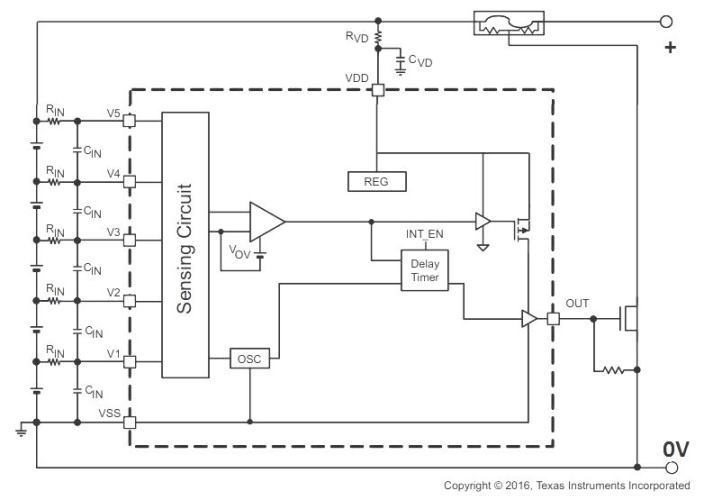 The supply input could be from a solar panel controller.
As soon as any of the series cell reaches an over voltage situation, first the delay timer activates, and waits for a while, and then ultimately the OUT pin is triggered ON to shunt down the supply.
The repeated OUTPUT ON/OFF switching allows the other cells to continue the charging process, and also simultaneously keeps the fully charged series cells from overcharging.
The supply input could be from a solar panel controller.
As soon as any of the series cell reaches an over voltage situation, first the delay timer activates, and waits for a while, and then ultimately the OUT pin is triggered ON to shunt down the supply.
The repeated OUTPUT ON/OFF switching allows the other cells to continue the charging process, and also simultaneously keeps the fully charged series cells from overcharging.
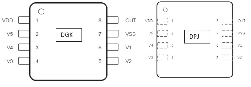 VDD is the power supply (30 V max, while 25V is recommended) while VSS is the reference ground or negative terminal.
A series resistor must connect with VDD to limit the current and capacitor should be connected to VSS pin to filter the noise.
V1 to V5 pins are used for sense input voltages in cell 1 to cell 5 respectively.
Out pin is used for overvoltage (voltage range -0.3 to 30) fault signal in battery pack.
VDD is the power supply (30 V max, while 25V is recommended) while VSS is the reference ground or negative terminal.
A series resistor must connect with VDD to limit the current and capacitor should be connected to VSS pin to filter the noise.
V1 to V5 pins are used for sense input voltages in cell 1 to cell 5 respectively.
Out pin is used for overvoltage (voltage range -0.3 to 30) fault signal in battery pack.
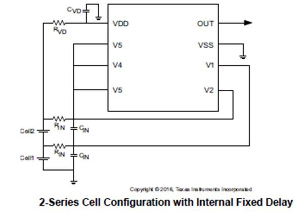 The manufacturerˇŻs recommendations shall be followed for the development of overvoltage protection circuits for battery pack.
Any alteration in ranges stated in data sheet may impact the accuracy of the cellˇŻs voltage measurement.
The calibration of device has been done using value = 1 k¦¸, the accuracy of device can be changed if other value of is used for calibration.
The manufacturerˇŻs recommendations shall be followed for the development of overvoltage protection circuits for battery pack.
Any alteration in ranges stated in data sheet may impact the accuracy of the cellˇŻs voltage measurement.
The calibration of device has been done using value = 1 k¦¸, the accuracy of device can be changed if other value of is used for calibration.
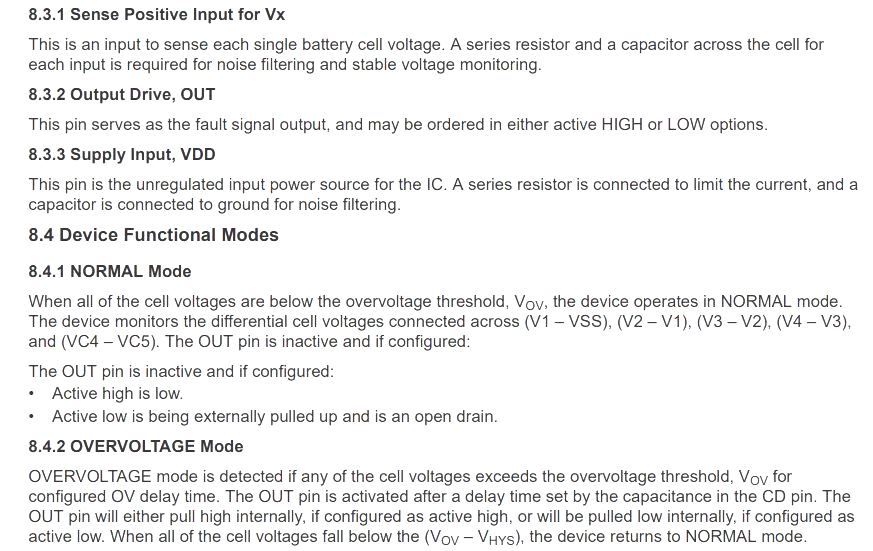 References:
https://www.ti.com/lit/ds/symlink/bq7718.pdf
Affanni, A., Bellini, A., Franceschini, G., Guglielmi, P., & Tassoni, C.
(2005).
Battery choice and management for new-generation electric vehicles.IEEE transactions on industrial electronics,52(5), 1343-1349.
References:
https://www.ti.com/lit/ds/symlink/bq7718.pdf
Affanni, A., Bellini, A., Franceschini, G., Guglielmi, P., & Tassoni, C.
(2005).
Battery choice and management for new-generation electric vehicles.IEEE transactions on industrial electronics,52(5), 1343-1349.
 The lambda diode represented inside the dashed box is built using a pair of n- and p-channel FET's.
Remember that there's no ready made "lambda" diode available in the market.
Practically, a lambda diode is built by interconnecting two low power FETs, and is operated using only two terminals, marked "anode" (A) and "cathode" (K).
When the biasing over this lambda diode is in the cut off mode, transistor Q3 is also switched off, which in turn keeps the LED1 is off.
As the battery voltage begins falling, it reaches a point where the lambda diode suddenly gets biased and conducts.
This situation instantly biases Q3 into conduction which powers ON the LED alerting the user regarding the low-battery condition.
(The working characteristic of the lambda diode can be witnessed below).
The lambda diode represented inside the dashed box is built using a pair of n- and p-channel FET's.
Remember that there's no ready made "lambda" diode available in the market.
Practically, a lambda diode is built by interconnecting two low power FETs, and is operated using only two terminals, marked "anode" (A) and "cathode" (K).
When the biasing over this lambda diode is in the cut off mode, transistor Q3 is also switched off, which in turn keeps the LED1 is off.
As the battery voltage begins falling, it reaches a point where the lambda diode suddenly gets biased and conducts.
This situation instantly biases Q3 into conduction which powers ON the LED alerting the user regarding the low-battery condition.
(The working characteristic of the lambda diode can be witnessed below).
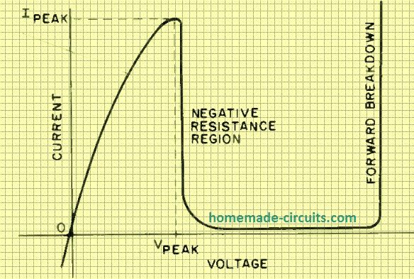 The potential level which biases the lambda diode into conduction is totally adjustable through the potentiometer R1.
Resistor R2 is wired like a current limiter for safeguarding LED1. The value of this current limiting resistors can be calculated using Ohm's Law (R2 = E/I, where R2 is in ohms, E represents the Ni-Cd battery potential threshold where the LED1 just illuminates, and I should be replaced with the maximum safe current value for the LED.
The potential level which biases the lambda diode into conduction is totally adjustable through the potentiometer R1.
Resistor R2 is wired like a current limiter for safeguarding LED1. The value of this current limiting resistors can be calculated using Ohm's Law (R2 = E/I, where R2 is in ohms, E represents the Ni-Cd battery potential threshold where the LED1 just illuminates, and I should be replaced with the maximum safe current value for the LED.
 The JFET type for building the lambda diode is actually not critical.
Nearly all configurations involving n- and p -channel FETs should perform well, along with the ones that are specified in the parts list.
If required you can consider replacing the LED1 with a low power relay to enable disconnection of the Ni-Cad battery pack from the load as soon as the voltage level drops below the critical low threshold.
This particular arrangement will automatically safeguard the battery pack from polarity reversal while it is being discharged.
The JFET type for building the lambda diode is actually not critical.
Nearly all configurations involving n- and p -channel FETs should perform well, along with the ones that are specified in the parts list.
If required you can consider replacing the LED1 with a low power relay to enable disconnection of the Ni-Cad battery pack from the load as soon as the voltage level drops below the critical low threshold.
This particular arrangement will automatically safeguard the battery pack from polarity reversal while it is being discharged.
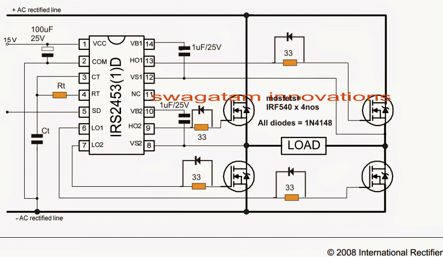 As shown in the above image, basically, in a full-bridge inverter we have a set of 4 MOSFETs connected to the output load.
The diagonally connected MOSFET pairs are alternately switched through an external oscillator, causing the input DC from the battery to transform into an alternating current or AC for the load.
The load is normally in the form of a transformer, whose low voltage primary is connected with the MOSFET bridge for the intended DC to AC inversion.
Typically, the 4 N-channel MOSFET based H-bridge topology is applied in full bridge inverters, since this topology provides the most efficient working in terms of compactness to power output ratio.
Although using 4 N channel inverters depend on specialized driver ICs with bootstrapping, yet the efficiency overweighs the complexity, hence these types are popularly employed in all modern full bridge inverters.
As shown in the above image, basically, in a full-bridge inverter we have a set of 4 MOSFETs connected to the output load.
The diagonally connected MOSFET pairs are alternately switched through an external oscillator, causing the input DC from the battery to transform into an alternating current or AC for the load.
The load is normally in the form of a transformer, whose low voltage primary is connected with the MOSFET bridge for the intended DC to AC inversion.
Typically, the 4 N-channel MOSFET based H-bridge topology is applied in full bridge inverters, since this topology provides the most efficient working in terms of compactness to power output ratio.
Although using 4 N channel inverters depend on specialized driver ICs with bootstrapping, yet the efficiency overweighs the complexity, hence these types are popularly employed in all modern full bridge inverters.
 The anode of the diode is connected with the source pin, while the cathode pin is associated with the drain pin of the device.
We can also see that since the MOSFETs are configured in a bridged network, the diodes also become configured in a basic full-bridge rectifier network format.
A couple of relays are employed which implement a few quick changeovers for enabling the grid AC to charge the battery via the MOSFET body diodes.
This bridge rectifier network formation of the MOSFET internal diodes actually makes the process of using a single transformer as an inverter transformer and charger transformer very straightforward.
The anode of the diode is connected with the source pin, while the cathode pin is associated with the drain pin of the device.
We can also see that since the MOSFETs are configured in a bridged network, the diodes also become configured in a basic full-bridge rectifier network format.
A couple of relays are employed which implement a few quick changeovers for enabling the grid AC to charge the battery via the MOSFET body diodes.
This bridge rectifier network formation of the MOSFET internal diodes actually makes the process of using a single transformer as an inverter transformer and charger transformer very straightforward.
 With an AC supply, the transformer wires change their polarity alternately.
As shown in the left image, assuming the START as the positive wire, the orange arrows indicate the flow pattern of current via D1, battery, D3 and back to the FINISH or the negative wire of the transformer.
For the next AC cycle, the polarity reverses, and the current moves as indicated by the blue arrows via body diode D4, battery, D2, and back to the FINISH or the negative end of the transformer winding.
This keeps repeating alternately, transforming both the AC cycles to DC and charging the battery.
However, since MOSFETs are also involved in the system, extreme care has to be exercised to ensure that these device do not get damaged in the process, and this calls for a perfect inverter/charger changeover operations.
With an AC supply, the transformer wires change their polarity alternately.
As shown in the left image, assuming the START as the positive wire, the orange arrows indicate the flow pattern of current via D1, battery, D3 and back to the FINISH or the negative wire of the transformer.
For the next AC cycle, the polarity reverses, and the current moves as indicated by the blue arrows via body diode D4, battery, D2, and back to the FINISH or the negative end of the transformer winding.
This keeps repeating alternately, transforming both the AC cycles to DC and charging the battery.
However, since MOSFETs are also involved in the system, extreme care has to be exercised to ensure that these device do not get damaged in the process, and this calls for a perfect inverter/charger changeover operations.
 To ensure 100% safety for the MOSFETs in the charging mode and while using the body diodes with the transformer AC, the MOSFET gates must be held at the ground potential, and completely cut-off from the supply DC.
For this we implement two things, connect 1 k resistors across the gate/source pins of all the MOSFETs, and a put a cut-off relay in series with the Vcc supply line of the driver IC.
The cut-off relay is an SPDT relay contact with its N/C contacts connected in series with the driver IC supply input.
In the absence of AC mains, the N/C contacts remain active allowing the battery supply to reach the driver IC for powering the MOSFETs.
When mains AC is available, this relay changes over to the N/O contacts cutting off the IC Vcc from the power source, thus ensuring a total cut off for the MOSFETs from the positive drive.
We can see another set of relay contacts connected with the transformer 220 V mains side.
This winding constitutes the output 220V side of the inverter.
The winding ends are connected with the poles of a DPDT relay, whose N/O an N/C contacts are configured with the mains grid input AC and the load respectively.
In the absence of mains grid AC, the system works in the inverter mode, and the power output is delivered to the load via the N/C contacts of the DPDT.
In the presence of an AC grid input, the relay activates to N/O contacts allowing the grid AC to power the 220V side of the transformer.
This in turn energizes the inverter side of the transformer and the current is allowed to pass through the body diodes of the MOSFETs for charging the attached battery.
Before the DPDT relay is able to activate, the SPDT relay is supposed to cut off the Vcc of the driver IC from the supply.
This slight delay in activation between the SPDT relay and the DPDT relay must be ensured in order to guarantee 100% safety for the MOSFETs and for the sound operations of the inverter/charging mode via the body diodes.
To ensure 100% safety for the MOSFETs in the charging mode and while using the body diodes with the transformer AC, the MOSFET gates must be held at the ground potential, and completely cut-off from the supply DC.
For this we implement two things, connect 1 k resistors across the gate/source pins of all the MOSFETs, and a put a cut-off relay in series with the Vcc supply line of the driver IC.
The cut-off relay is an SPDT relay contact with its N/C contacts connected in series with the driver IC supply input.
In the absence of AC mains, the N/C contacts remain active allowing the battery supply to reach the driver IC for powering the MOSFETs.
When mains AC is available, this relay changes over to the N/O contacts cutting off the IC Vcc from the power source, thus ensuring a total cut off for the MOSFETs from the positive drive.
We can see another set of relay contacts connected with the transformer 220 V mains side.
This winding constitutes the output 220V side of the inverter.
The winding ends are connected with the poles of a DPDT relay, whose N/O an N/C contacts are configured with the mains grid input AC and the load respectively.
In the absence of mains grid AC, the system works in the inverter mode, and the power output is delivered to the load via the N/C contacts of the DPDT.
In the presence of an AC grid input, the relay activates to N/O contacts allowing the grid AC to power the 220V side of the transformer.
This in turn energizes the inverter side of the transformer and the current is allowed to pass through the body diodes of the MOSFETs for charging the attached battery.
Before the DPDT relay is able to activate, the SPDT relay is supposed to cut off the Vcc of the driver IC from the supply.
This slight delay in activation between the SPDT relay and the DPDT relay must be ensured in order to guarantee 100% safety for the MOSFETs and for the sound operations of the inverter/charging mode via the body diodes.
 Here, the operational DC supply for the relay coil is acquired from a standard AC to DC adapter, plugged with the grid mains.
This means, when grid AC is available, the AC/DC adapter powers ON the relays.
The SPDT relay being connected directly to the DC supply activates quickly before the DPDT relay can.
The DPDT relay activates a few milliseconds later due to the presence of the 10 ohm and the 470 uF capacitor.
This ensures that the MOSFET driver IC is disabled before the transformer is able to respond to the grid AC input at its 220 V side.
When mains AC fails, both the relay switch OFF almost simultaneously, since the 470uF capacitor now has no effect on the DPDT due to the series reverse biased diode.
This concludes our explanation regarding using MOSFET body diodes for charging an inverter battery through a single common transformer.
Hopefully, the idea will allow the many hobbyists to build cheap, compact automatic inverters with built-in battery chargers, using a single common transformer.
Here, the operational DC supply for the relay coil is acquired from a standard AC to DC adapter, plugged with the grid mains.
This means, when grid AC is available, the AC/DC adapter powers ON the relays.
The SPDT relay being connected directly to the DC supply activates quickly before the DPDT relay can.
The DPDT relay activates a few milliseconds later due to the presence of the 10 ohm and the 470 uF capacitor.
This ensures that the MOSFET driver IC is disabled before the transformer is able to respond to the grid AC input at its 220 V side.
When mains AC fails, both the relay switch OFF almost simultaneously, since the 470uF capacitor now has no effect on the DPDT due to the series reverse biased diode.
This concludes our explanation regarding using MOSFET body diodes for charging an inverter battery through a single common transformer.
Hopefully, the idea will allow the many hobbyists to build cheap, compact automatic inverters with built-in battery chargers, using a single common transformer.
 Design Courtesy: Elektor Electronics
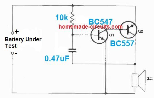 When an exhausted cell is placed, a note around 1 kHz is provided.
The device has been examined with battery voltages between 1.5 V and 14 V, utilizing a BC547 as Q1 and an BC557 as Q2.
You can also use the battery in the reverse polarity and still make the circuit work without any problems.
When an exhausted cell is placed, a note around 1 kHz is provided.
The device has been examined with battery voltages between 1.5 V and 14 V, utilizing a BC547 as Q1 and an BC557 as Q2.
You can also use the battery in the reverse polarity and still make the circuit work without any problems.
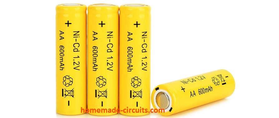 The simple Ni-Cad charger circuit presented below effectively tackles the overcharging criterion by including facilities like a constant current charging as well as cutting off the supply when the cell terminal reaches the full charge value.
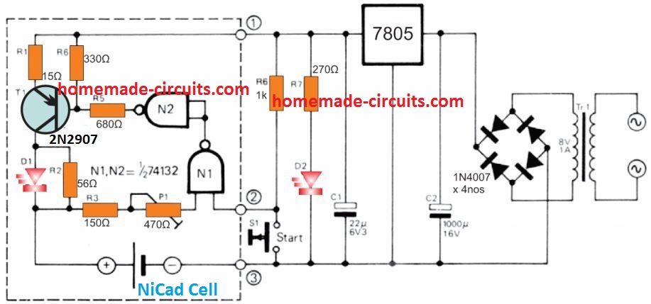
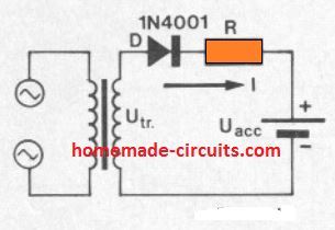 This is often accomplished rather easily by charging via a resistor from a supply voltage many times higher than the battery voltage.
Change in the battery voltage as it charges will likely then have minimal influence on the charge current.
The proposed circuit is made up just a transformer, diode rectifier and series resistor as indicated in figure 1.
The associated graphical image facilitates the necessary series resistor value to be determined.
This is often accomplished rather easily by charging via a resistor from a supply voltage many times higher than the battery voltage.
Change in the battery voltage as it charges will likely then have minimal influence on the charge current.
The proposed circuit is made up just a transformer, diode rectifier and series resistor as indicated in figure 1.
The associated graphical image facilitates the necessary series resistor value to be determined.
 A horizontal line is drawn through the transformer voltage on the vertical axis until it crosses the specified battery voltage line.
Then, a line pulled vertically down from this point to meet the horizontal axis subsequently provides us the necessary resistor value in ohms.
For instance, the dotted line demonstrates that if the transformer voltage is 18 V and the Ni-Cd battery to be charged is 6 V, then the resistance value will be around 36 ohms for the intended current control.
This indicated resistance is calculated to deliver 120 mA, while for some other charging current rates the resistor value will need to be reduced down appropriately, e.g.
18 ohms for 240 mA, 72 ohms for 60 mA etc.
D1.
A horizontal line is drawn through the transformer voltage on the vertical axis until it crosses the specified battery voltage line.
Then, a line pulled vertically down from this point to meet the horizontal axis subsequently provides us the necessary resistor value in ohms.
For instance, the dotted line demonstrates that if the transformer voltage is 18 V and the Ni-Cd battery to be charged is 6 V, then the resistance value will be around 36 ohms for the intended current control.
This indicated resistance is calculated to deliver 120 mA, while for some other charging current rates the resistor value will need to be reduced down appropriately, e.g.
18 ohms for 240 mA, 72 ohms for 60 mA etc.
D1.
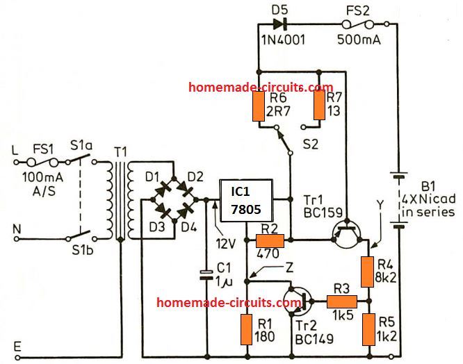 In the discussed NiCad charger circuit R1 and R2 fix the off-load output voltage to approximately 8V.
The output current travels by means of either R6 or R7, and as it rises transistor Tr1 is gradually switched on.
This causes point Y to increase, switching on transistor Tr2 and enabling point Z to become less an less positive.
The process consequently decreases the output voltage and has a tendency to bring down the current.
A balance level is ultimately attained which is determined by the value of R6 and R7.
Diode D5 inhibits the battery which is being charged, providing supply to the IC1 output in case of the 12V is removed, which could otherwise cause serious damage to the IC.
FS2 is incorporated to protect against damage to the batteries which are under charge.
Choice of R6 and R7 is done through some trial and error, which means you will need an ammeter having a suitable range, or, if R6 and R7 values are genuinely known, then the voltage drop across them could be calculated through Ohm's Law.
In the discussed NiCad charger circuit R1 and R2 fix the off-load output voltage to approximately 8V.
The output current travels by means of either R6 or R7, and as it rises transistor Tr1 is gradually switched on.
This causes point Y to increase, switching on transistor Tr2 and enabling point Z to become less an less positive.
The process consequently decreases the output voltage and has a tendency to bring down the current.
A balance level is ultimately attained which is determined by the value of R6 and R7.
Diode D5 inhibits the battery which is being charged, providing supply to the IC1 output in case of the 12V is removed, which could otherwise cause serious damage to the IC.
FS2 is incorporated to protect against damage to the batteries which are under charge.
Choice of R6 and R7 is done through some trial and error, which means you will need an ammeter having a suitable range, or, if R6 and R7 values are genuinely known, then the voltage drop across them could be calculated through Ohm's Law.
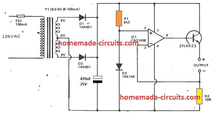 The charger should therefore include a circuit to restrict the charge current to a correct limit.
In this circuit, T1, D1, D2, and C1 work like a traditional step-down, isolation, full-wave rectifier, and DC filtering circuit.
The additional parts offer the current regulation.
IC1 is employed like a comparator with a separate buffer stage Q1 providing a appositely high output current functionality in this design.
IC1's non-inverting input is supplied with a 0.65 V: reference voltage presented through R1 and D3. The inverting input is connected to ground through R2 within quiescent current levels, allowing the output to get completely positive.
Having a NiCad cell attached across the output, a high current may make an effort to via R2, causing an equivalent amount of voltage to develop across R2.
It might merely increase to 0.6V, nevertheless, an increasing voltage at this point reverses the input potentials of the IC1 inputs, causing the output voltage to be reduced, and lowering the voltage around R2 back 0.65 V.
The highest output current (and also the charge current received) is as a result the current generated with 0.65 V across 10 ohms, or 65 mA put simply.
Most AA NiCad cells possess a optimum preferred charge current of no more than 45 or 50 mA, and for this category R2 must be increased to 13 ohms so that you can have the appropriate charge current.
A few rapid charger varieties may work with 150 mA, and this demands lowering R2 to 4.3 ohms (3.3 ohms plus 1 ohm in series in case a ideal part cannot be procured).
Furthermore, T1 needs to be improved to a variant with a current rating of 250 mA., and Q1 must be installed using a tiny bolt-on finned heatsink.
The device can easily charge up to four cells (6 cells when T1 is upgraded to a 12 V type), and all these should be attached in series over the output, and not in parallel.
The charger should therefore include a circuit to restrict the charge current to a correct limit.
In this circuit, T1, D1, D2, and C1 work like a traditional step-down, isolation, full-wave rectifier, and DC filtering circuit.
The additional parts offer the current regulation.
IC1 is employed like a comparator with a separate buffer stage Q1 providing a appositely high output current functionality in this design.
IC1's non-inverting input is supplied with a 0.65 V: reference voltage presented through R1 and D3. The inverting input is connected to ground through R2 within quiescent current levels, allowing the output to get completely positive.
Having a NiCad cell attached across the output, a high current may make an effort to via R2, causing an equivalent amount of voltage to develop across R2.
It might merely increase to 0.6V, nevertheless, an increasing voltage at this point reverses the input potentials of the IC1 inputs, causing the output voltage to be reduced, and lowering the voltage around R2 back 0.65 V.
The highest output current (and also the charge current received) is as a result the current generated with 0.65 V across 10 ohms, or 65 mA put simply.
Most AA NiCad cells possess a optimum preferred charge current of no more than 45 or 50 mA, and for this category R2 must be increased to 13 ohms so that you can have the appropriate charge current.
A few rapid charger varieties may work with 150 mA, and this demands lowering R2 to 4.3 ohms (3.3 ohms plus 1 ohm in series in case a ideal part cannot be procured).
Furthermore, T1 needs to be improved to a variant with a current rating of 250 mA., and Q1 must be installed using a tiny bolt-on finned heatsink.
The device can easily charge up to four cells (6 cells when T1 is upgraded to a 12 V type), and all these should be attached in series over the output, and not in parallel.
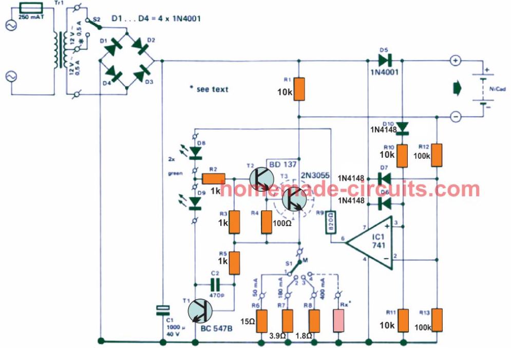 The current source becomes active only when the NiCad cells are attached the correct way round.
ICI is positioned to check the network by verifying the voltage polarity across the output terminals.
If the cells are rigged properly, pin 2 of IC1 is not able to turn as positive as on pin 3.
As a result IC1 output gets positive and resources a base current to T2, which turns on the current source.
The current source limit could be fixed using S1. A current of 50 mA, 180 mA and 400 mA could be preset once the values of R6,R7 and RB are determined.
Putting S1 at point 1 shows that the NiCad cells can be charged, position 2 is intended for C cells and position 3 is reserved of D cells.
The current source becomes active only when the NiCad cells are attached the correct way round.
ICI is positioned to check the network by verifying the voltage polarity across the output terminals.
If the cells are rigged properly, pin 2 of IC1 is not able to turn as positive as on pin 3.
As a result IC1 output gets positive and resources a base current to T2, which turns on the current source.
The current source limit could be fixed using S1. A current of 50 mA, 180 mA and 400 mA could be preset once the values of R6,R7 and RB are determined.
Putting S1 at point 1 shows that the NiCad cells can be charged, position 2 is intended for C cells and position 3 is reserved of D cells.
 Miscellaneous Parts
TR1 = transformer 2 x 12 V/0.5 A
S1 = 3 position switch
S2 = 2 position switch
The current source works using a very basic principle.
The circuit is wired like a current feedback network.
Imagine S1 to be at position 1 and IC1 output is positive.
T2 and 13 now begin getting a base current and initiate conduction.
The current via these transistors constitutes a voltage around R6, which triggers T1 into operation.
An escalating current around R6 signifies that T1 can conduct with greater strength thus minimizing the base drive current for transistors T2 and T3.
The second transistor can at this point conduct less and the initial current rise is restricted.
A reasonably constant current by means of R3 and the attached NiCad cells thus gets implemented.
A couple of LED's attached to the current source indicate the operational status the NiCad charger at any instant.
IC1 resources a positive voltage once the NiCad cells are hooked up in the right way illuminating the LED D8.
If the cells are not connected with correct polarity, the positive potential at pin 2 of IC1 will be higher than pin 3, causing the op amp comparator output to become 0 V.
In this situation the current source will remain switched off and LED D8 will not illuminate.
An identical condition can transpire in case no cells are connected for charging.
This may happen because pin 2 will possess an increased voltage compared to pin 3, due to the voltage drop across D10.
The charger will only activate when a cell comprising of a minimum of 1 V is joined.
LED D9 shows that the current source is operating like a current source.
This might appear quite peculiar, however an input current generated by IC1 just isn't adequate, the voltage level also needs to be large enough to reinforce the current.
This implies that the supply should always be greater than the voltage across the NiCad cells.
Only in this situation the potential difference will be sufficient for the current feedback T1 to kick-in, illuminating the LED D9.
Miscellaneous Parts
TR1 = transformer 2 x 12 V/0.5 A
S1 = 3 position switch
S2 = 2 position switch
The current source works using a very basic principle.
The circuit is wired like a current feedback network.
Imagine S1 to be at position 1 and IC1 output is positive.
T2 and 13 now begin getting a base current and initiate conduction.
The current via these transistors constitutes a voltage around R6, which triggers T1 into operation.
An escalating current around R6 signifies that T1 can conduct with greater strength thus minimizing the base drive current for transistors T2 and T3.
The second transistor can at this point conduct less and the initial current rise is restricted.
A reasonably constant current by means of R3 and the attached NiCad cells thus gets implemented.
A couple of LED's attached to the current source indicate the operational status the NiCad charger at any instant.
IC1 resources a positive voltage once the NiCad cells are hooked up in the right way illuminating the LED D8.
If the cells are not connected with correct polarity, the positive potential at pin 2 of IC1 will be higher than pin 3, causing the op amp comparator output to become 0 V.
In this situation the current source will remain switched off and LED D8 will not illuminate.
An identical condition can transpire in case no cells are connected for charging.
This may happen because pin 2 will possess an increased voltage compared to pin 3, due to the voltage drop across D10.
The charger will only activate when a cell comprising of a minimum of 1 V is joined.
LED D9 shows that the current source is operating like a current source.
This might appear quite peculiar, however an input current generated by IC1 just isn't adequate, the voltage level also needs to be large enough to reinforce the current.
This implies that the supply should always be greater than the voltage across the NiCad cells.
Only in this situation the potential difference will be sufficient for the current feedback T1 to kick-in, illuminating the LED D9.
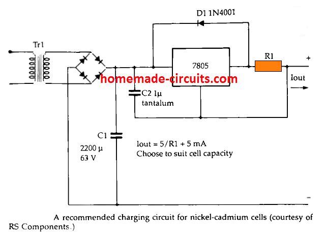 This employs a 7805 regulator IC to deliver a constant 5V across a resistor, which causes the current to be dependent on the value of resistor, instead of on the cell potential.
The value of the resistor should be adjusted with regard to the type that is used for charging; any value between 10 Ohm to 470 Ohm could be used depending on the cell mAh rating.
Due to the floating nature of the IC 7805 with respect to the ground potential, this design could be applied for charging individual Nicad cells or series of a few cells.
This employs a 7805 regulator IC to deliver a constant 5V across a resistor, which causes the current to be dependent on the value of resistor, instead of on the cell potential.
The value of the resistor should be adjusted with regard to the type that is used for charging; any value between 10 Ohm to 470 Ohm could be used depending on the cell mAh rating.
Due to the floating nature of the IC 7805 with respect to the ground potential, this design could be applied for charging individual Nicad cells or series of a few cells.
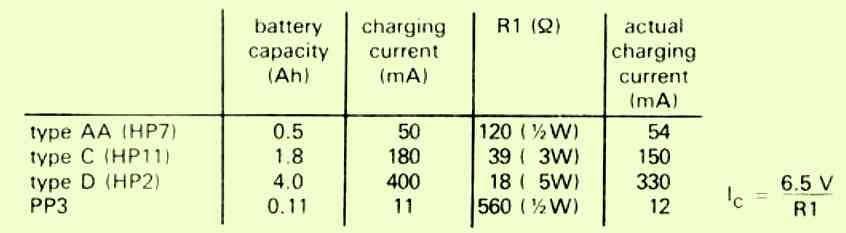 The circuit includes a small extra feature which is the LED connected in series with the ground pin of the regulator lC.
This LED is configured to work like a NiCd charging indicator.
A predetermined current of 8mA +/-1 mA, that is determined by the preferred output current and which should be incorporated to this output current, runs by means of the LED.
While fixing the value of the resistor R1, it is crucial to rememeber about the extra 1.5 V dropped across the LED.
As already considered, this current source is utilized as the charging current for NiCad batteries.
As opposed to lead-acid batteries NiCd batteries must be charged with a constant current.
Typical NiCads needs to be charged with a current that must be 1/10th value of its mAH rating, and charged for a approximate duration of 14 hours.
It is always recommended to ensure that the NiCd cell is fully always discharged, and then quickly connected to a charger.
This will enable the cell to have a longer life and provide higher number of charge/discharge cycles.
The circuit includes a small extra feature which is the LED connected in series with the ground pin of the regulator lC.
This LED is configured to work like a NiCd charging indicator.
A predetermined current of 8mA +/-1 mA, that is determined by the preferred output current and which should be incorporated to this output current, runs by means of the LED.
While fixing the value of the resistor R1, it is crucial to rememeber about the extra 1.5 V dropped across the LED.
As already considered, this current source is utilized as the charging current for NiCad batteries.
As opposed to lead-acid batteries NiCd batteries must be charged with a constant current.
Typical NiCads needs to be charged with a current that must be 1/10th value of its mAH rating, and charged for a approximate duration of 14 hours.
It is always recommended to ensure that the NiCd cell is fully always discharged, and then quickly connected to a charger.
This will enable the cell to have a longer life and provide higher number of charge/discharge cycles.
 C3 gets charged through D2 and D3 to almost 12 V when pin 3 is a logic low.
The moment pin 3 is logic high, the junction voltage of C3 and D3 boosts to 24 V due to the negative terminal of C3 which is plugged at +12 V, and the capacitor itself holds a charge of the same value.
Then, diode D3 becomes reverse biased, but D4 conducts just enough for C4 to get charged over 20 V.
This is more than enough voltage for our circuit.
The 78L05 in the IC2 positions acts as a current supplier which happens to hold its output voltage, Un, from appearing across R3 at 5 V.
The output current, In, can be simply calculated from the equation:
I¦Ç = U¦Ç / R3 = 5 / 680 = 7.4 mA
The properties of the 78L05 include drawing current itself as the central terminal (usually earthed) gives ours around 3 mA.
The total load current is about 10 mA and that is a good value for constantly charging NiCd batteries.
To display that charging current is flowing, an LED is included in the circuit.
C3 gets charged through D2 and D3 to almost 12 V when pin 3 is a logic low.
The moment pin 3 is logic high, the junction voltage of C3 and D3 boosts to 24 V due to the negative terminal of C3 which is plugged at +12 V, and the capacitor itself holds a charge of the same value.
Then, diode D3 becomes reverse biased, but D4 conducts just enough for C4 to get charged over 20 V.
This is more than enough voltage for our circuit.
The 78L05 in the IC2 positions acts as a current supplier which happens to hold its output voltage, Un, from appearing across R3 at 5 V.
The output current, In, can be simply calculated from the equation:
I¦Ç = U¦Ç / R3 = 5 / 680 = 7.4 mA
The properties of the 78L05 include drawing current itself as the central terminal (usually earthed) gives ours around 3 mA.
The total load current is about 10 mA and that is a good value for constantly charging NiCd batteries.
To display that charging current is flowing, an LED is included in the circuit.
 The circuitˇŻs output voltage seems to drop with the escalating current.
The voltage drop across the 78L05 is around 5 V.
But, an additional 2.5 V must be included to ensure the IC operates precisely.
Across the LED, there is most likely a 1.5 V voltage drop.
Considering all the above, a 12 V NiCd battery with a rated capacity of 500 mAh could be charged uninterruptedly using a current of 5 mA.
In total, it is only 1% of its capacity.
The circuitˇŻs output voltage seems to drop with the escalating current.
The voltage drop across the 78L05 is around 5 V.
But, an additional 2.5 V must be included to ensure the IC operates precisely.
Across the LED, there is most likely a 1.5 V voltage drop.
Considering all the above, a 12 V NiCd battery with a rated capacity of 500 mAh could be charged uninterruptedly using a current of 5 mA.
In total, it is only 1% of its capacity.

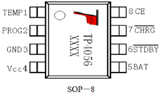 Datasheet TP4056
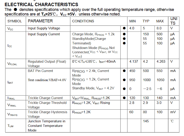
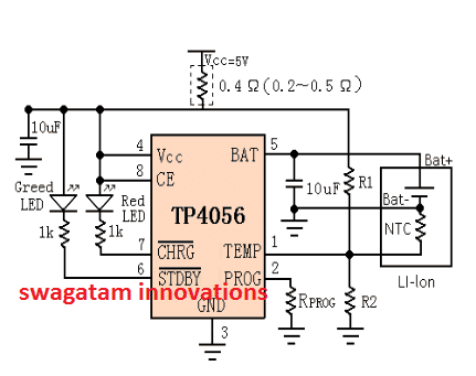 The following figure shows the LED status indication details for the above discussed CV, CC Li-Ion battery charger circuit.
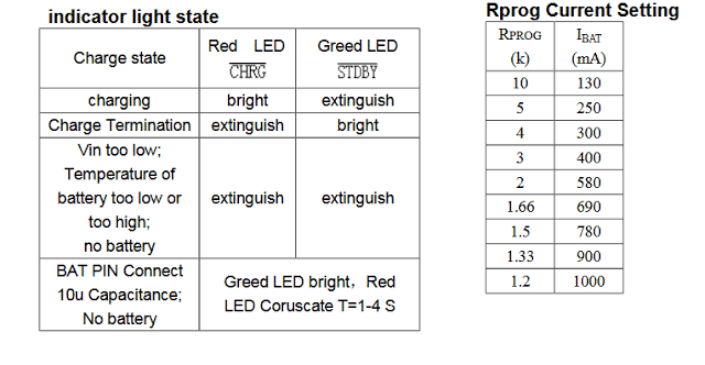 Courtesy: NanJing Top Power ASIC Corp.
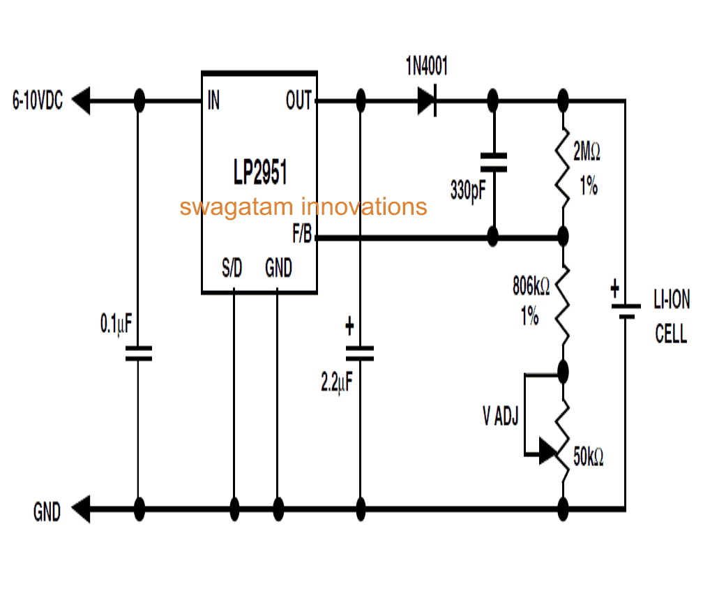
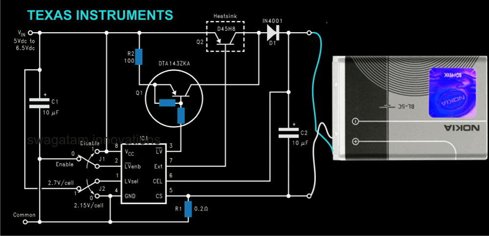 These were the assorted top 3 smart, intelligent Li-Ion Battery charger circuits for you, if you any more ideas or information regrading such smart designs, please feel free to express them through comments.
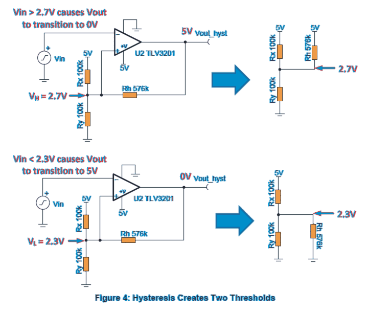
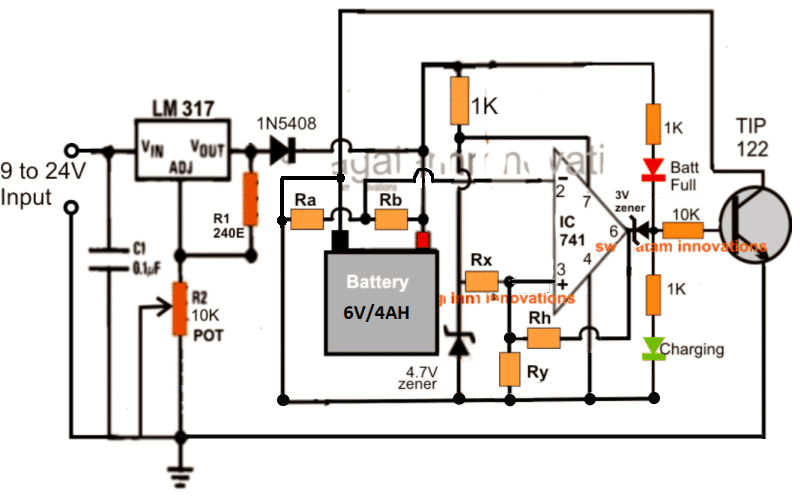
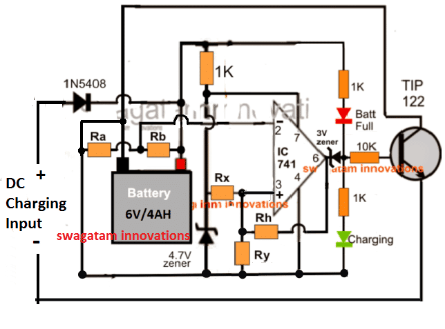 The calculation procedures will be exactly the same as expressed in the previous paragraph.
For high current battery charging, the TIP122 and the diode 1N5408 may need to be upgraded with proportionately higher current devices, and change the 4.7V zener to a value that may be higher than 50% of the battery voltage.
The green LED indicates the charging status of the battery while the red LED enables us to know when the battery is fully charged.
This concludes the article, which clearly explains how to make a simple yet universally applicable battery charger circuit using fixed resistors to ensure extreme accuracy and foolproof cut offs across the set threshold points, which in turn ensures perfect and a safe charging for the connected battery.
The calculation procedures will be exactly the same as expressed in the previous paragraph.
For high current battery charging, the TIP122 and the diode 1N5408 may need to be upgraded with proportionately higher current devices, and change the 4.7V zener to a value that may be higher than 50% of the battery voltage.
The green LED indicates the charging status of the battery while the red LED enables us to know when the battery is fully charged.
This concludes the article, which clearly explains how to make a simple yet universally applicable battery charger circuit using fixed resistors to ensure extreme accuracy and foolproof cut offs across the set threshold points, which in turn ensures perfect and a safe charging for the connected battery.
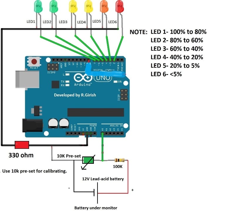 The circuit consists of Arduino which is the brain of the system, a potential divider which helps the Arduino to sample the input voltage.
A pre-set resistor is used to calibrate the above setup.
The series of 6 LEDs will indicate the battery level.
The circuit consists of Arduino which is the brain of the system, a potential divider which helps the Arduino to sample the input voltage.
A pre-set resistor is used to calibrate the above setup.
The series of 6 LEDs will indicate the battery level.
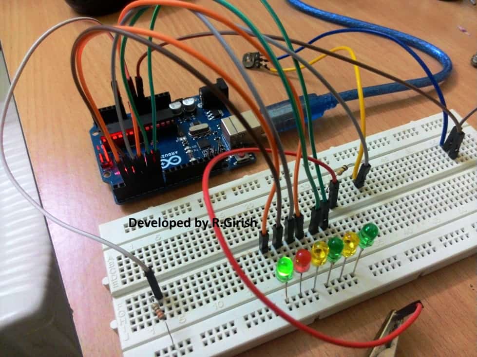
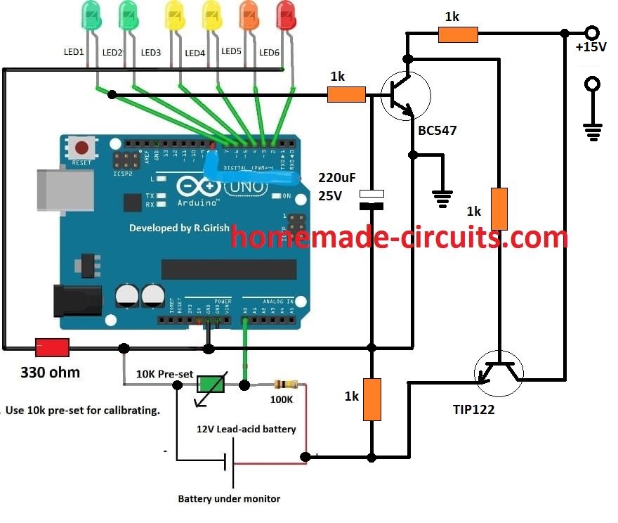
 The discussed over discharge protection circuit for 12v battery consists of a voltage divider which is responsible for stepping down the input voltage and reduce to narrow range where arduino can read the voltage.
The 10k pre-set resistor is used to calibrate the readings on arduino; these readings are used by arduino to trigger the relay, the calibration of this setup will be discussed later part of the article.
A LED indicator is utilized for indicating the status of the relay.
The transistor drives the relay on/off and a diode is connected across the relay for arresting high voltage spike generated from relay, while switching it on/off.
When the battery voltage goes below 11.80V, the relay gets turned on and disconnects the battery from load and LED indicator also turns on, this happen same when the circuit reads overvoltage from the battery, you can set the overvoltage cut-off in the program.
When the battery goes below 11.80V, the relay disconnect the load, the relay will reconnect the load to battery only after when the battery voltage attains above nominal voltage which is set in the program.
The nominal voltage is normal operating voltage of the load.
The above stated mechanism is done because; the battery voltage rise after disconnecting from load and this must not trigger the relay ON at low battery state.
The nominal voltage in the program set as 12.70 V which is full battery voltage of typical 12V SLA batteries (Full battery voltage after disconnecting from charger).
The discussed over discharge protection circuit for 12v battery consists of a voltage divider which is responsible for stepping down the input voltage and reduce to narrow range where arduino can read the voltage.
The 10k pre-set resistor is used to calibrate the readings on arduino; these readings are used by arduino to trigger the relay, the calibration of this setup will be discussed later part of the article.
A LED indicator is utilized for indicating the status of the relay.
The transistor drives the relay on/off and a diode is connected across the relay for arresting high voltage spike generated from relay, while switching it on/off.
When the battery voltage goes below 11.80V, the relay gets turned on and disconnects the battery from load and LED indicator also turns on, this happen same when the circuit reads overvoltage from the battery, you can set the overvoltage cut-off in the program.
When the battery goes below 11.80V, the relay disconnect the load, the relay will reconnect the load to battery only after when the battery voltage attains above nominal voltage which is set in the program.
The nominal voltage is normal operating voltage of the load.
The above stated mechanism is done because; the battery voltage rise after disconnecting from load and this must not trigger the relay ON at low battery state.
The nominal voltage in the program set as 12.70 V which is full battery voltage of typical 12V SLA batteries (Full battery voltage after disconnecting from charger).
 Video Clip:
 For users who wish to see the LED switch OFF at the upper threshold can use the above shown design, the working may be understood wit the following points:
As per the requirement the LED illumination is supposed to begin diminishing as soon as the battery reaches approximately close to the set full charge threshold.
The setting up procedure of the preset is actually very simple.
The user must feed a supply voltage that may be equal to desired high charge level of the battery, and then gently adjust the preset with a screw driver to force the LED to just shut down at the desired level..
For example suppose the indicator circuit is been installed for monitoring a 12V battery over charge level at 14.3V, then the preset may be tweaked to make sure that the LED just begins shutting down at around 14V.
For users who wish to see the LED switch OFF at the upper threshold can use the above shown design, the working may be understood wit the following points:
As per the requirement the LED illumination is supposed to begin diminishing as soon as the battery reaches approximately close to the set full charge threshold.
The setting up procedure of the preset is actually very simple.
The user must feed a supply voltage that may be equal to desired high charge level of the battery, and then gently adjust the preset with a screw driver to force the LED to just shut down at the desired level..
For example suppose the indicator circuit is been installed for monitoring a 12V battery over charge level at 14.3V, then the preset may be tweaked to make sure that the LED just begins shutting down at around 14V.
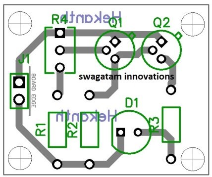
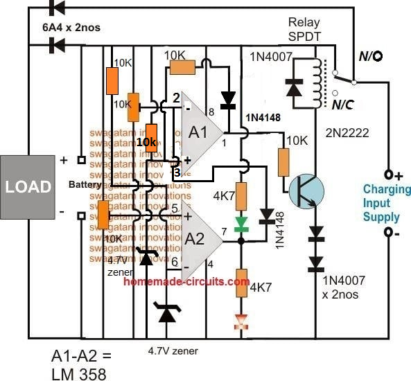 Note: Please replace the 10K in series with the 1N4148, with a 1K
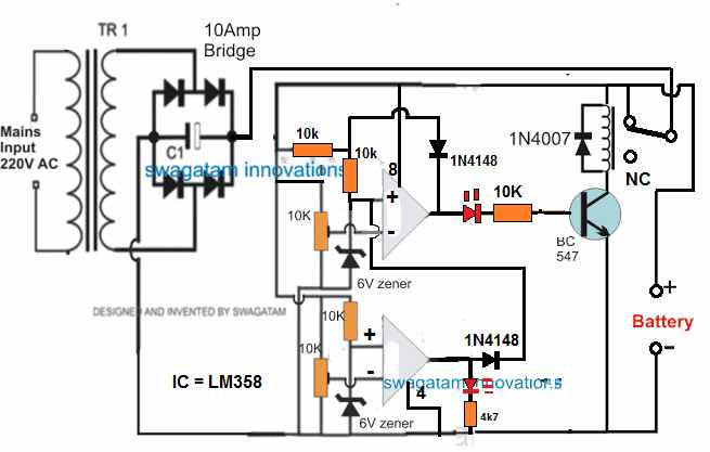
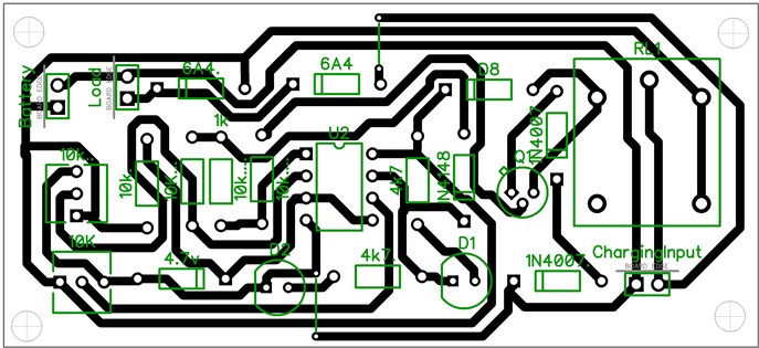
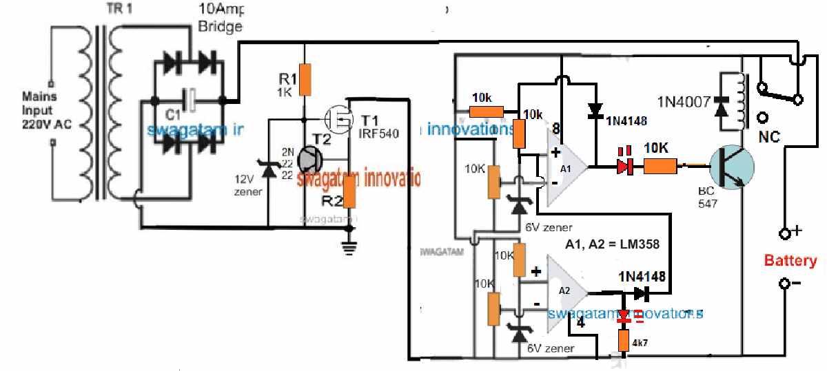 R2 = 0.6 / charging current
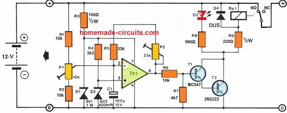
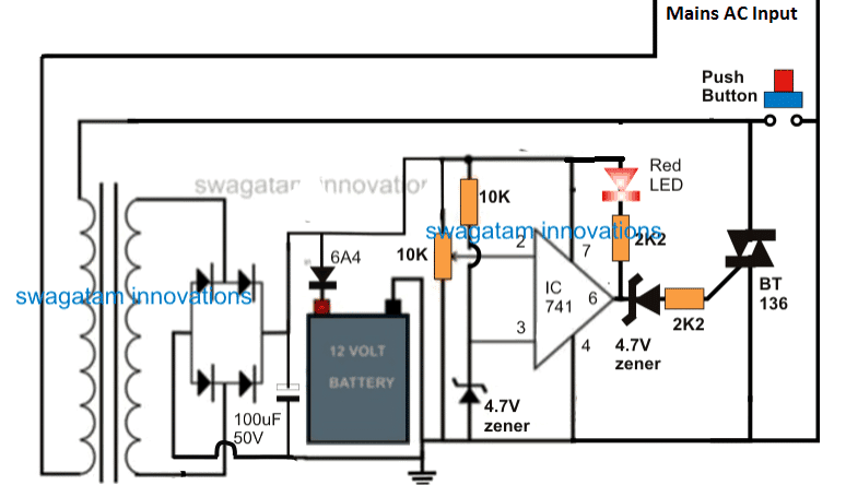 When mains power is applied the circuit does not switch ON by itself, and remains in a standby position.
The indicated push button is positioned for initiating the charging process, therefore as soon as this switch is pressed the triac ismomentarily shorted allowing the transformer to access the mains power
for that instant.
The above action also instantaneously allows the circuit to get powered for that particular period of time.
When mains power is applied the circuit does not switch ON by itself, and remains in a standby position.
The indicated push button is positioned for initiating the charging process, therefore as soon as this switch is pressed the triac ismomentarily shorted allowing the transformer to access the mains power
for that instant.
The above action also instantaneously allows the circuit to get powered for that particular period of time.

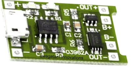
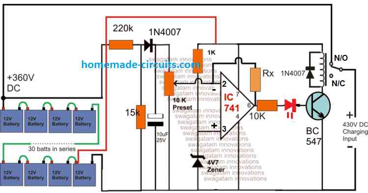

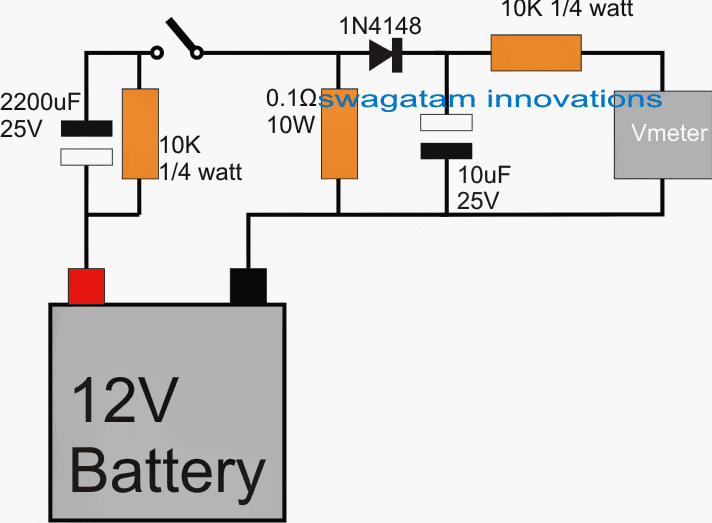 The diagram shows the proposed battery health checker circuit using very ordinary components and the set up hopefully can be used for determining the battery's overall condition by pressing ON the switch.
First the battery is charged to an optimal extent, this procedure cannot be avoided because unless the battery is properly charged the level of current it has retained cannot determined.
Hence after the battery is optimally charged using any ordinary high current battery charger, the above shown circuit set up can be attached with the battery for getting a rough idea regarding its AH efficiency specs.
The diagram shows the proposed battery health checker circuit using very ordinary components and the set up hopefully can be used for determining the battery's overall condition by pressing ON the switch.
First the battery is charged to an optimal extent, this procedure cannot be avoided because unless the battery is properly charged the level of current it has retained cannot determined.
Hence after the battery is optimally charged using any ordinary high current battery charger, the above shown circuit set up can be attached with the battery for getting a rough idea regarding its AH efficiency specs.
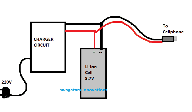 As can be seen in the above design, a charger circuit charges a 3.7V cell, once the charging is completed, the 3.7V cell box is carried by the user while traveling, and whenever the user's cellphone battery goes down, he simply connects this 3.7V cell pack with his cellphone for topping it up quickly.
As discussed in the previous paragraph, in order to enable the 3.7V power bank to be able to provide the required 4.2V at a consistent rate until the cellphone is completely charged at this level, a step up circuit becomes imperative.
As can be seen in the above design, a charger circuit charges a 3.7V cell, once the charging is completed, the 3.7V cell box is carried by the user while traveling, and whenever the user's cellphone battery goes down, he simply connects this 3.7V cell pack with his cellphone for topping it up quickly.
As discussed in the previous paragraph, in order to enable the 3.7V power bank to be able to provide the required 4.2V at a consistent rate until the cellphone is completely charged at this level, a step up circuit becomes imperative.
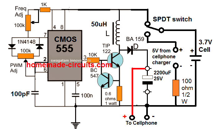
 Here, you can try 470 ohm, 1 watt resistor for R1, and 2N2222 transistor for T1.
1N5408 for D1, and a 1000uF/25V for C2.
Use 0.0047uF/100V for C1
The LED is not required, the LED points could be used as the output terminal for charging your smartphone
The coil is made over a T18 Torroidal ferrite core, with 20:10 turns for the primary and secondary, using multistarnd (7/36) flexible PVC insulated wire.
This may be implemented if the input is from a pack of 5nos of 1.5V AAA cells in parallel.
If you select Li-Ion cell at the input source, the ratio might need to be changed to 20:10 turns, 20 being at the base side of the coil.
The transistor might need a suitable heatsink in order to dissipate optimally.
Here, you can try 470 ohm, 1 watt resistor for R1, and 2N2222 transistor for T1.
1N5408 for D1, and a 1000uF/25V for C2.
Use 0.0047uF/100V for C1
The LED is not required, the LED points could be used as the output terminal for charging your smartphone
The coil is made over a T18 Torroidal ferrite core, with 20:10 turns for the primary and secondary, using multistarnd (7/36) flexible PVC insulated wire.
This may be implemented if the input is from a pack of 5nos of 1.5V AAA cells in parallel.
If you select Li-Ion cell at the input source, the ratio might need to be changed to 20:10 turns, 20 being at the base side of the coil.
The transistor might need a suitable heatsink in order to dissipate optimally.
 The part list will be the same as mentioned in the previous paragraph except the inductor, which will now have a 20:20 turn ratio using a 27SWG wire or any other suitable size magnet wire
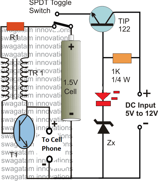 Here the TIP122 along with its base zener becomes a voltage regulator stage and is used as stabilized battery charger for the attached battery.
The Zx value determines the charging voltage, and its value must be selected such that it's always a shade lower than the actual full charge value of the battery.
For example if a Li-Ion battery is used, you may select Zx as 5.8V in order prevent the battery from overcharging.
From this 5.8V, the LED will drop around 1.2V, and the TIP122 will drop around 0.6V, which will ultimately allow the 3.7V cell to get around 4V, which is just around sufficient for the purpose.
For 1.5V AAA (5 in parallel), the zener could be replaced with a single 1N4007 diode with its cathode towards ground.
The LED is included for roughly indicating the full charge condition of the connected cell.
When the LED lights up brightly, you may assume the cell to be fully charged.
The DC input for the above charger circuit could be acquired from your normal cellphone AC/DC charger unit.
Although the above design is efficient and recommended for an optimal response, the idea may not be easy for a newcomer to build and optimize.
Therefore for users who might be OK with a slightly low tech design but much easier DIY alternative than the boost converter concept might be interested in the following configurations:
The three simple power bank circuit designs shown below utilizes minimum number of components and can be built by any new hobbyist within seconds
Although the designs look very straightforward, it demands the use of two 3.7V cells in series for the proposed power bank operations.
Here the TIP122 along with its base zener becomes a voltage regulator stage and is used as stabilized battery charger for the attached battery.
The Zx value determines the charging voltage, and its value must be selected such that it's always a shade lower than the actual full charge value of the battery.
For example if a Li-Ion battery is used, you may select Zx as 5.8V in order prevent the battery from overcharging.
From this 5.8V, the LED will drop around 1.2V, and the TIP122 will drop around 0.6V, which will ultimately allow the 3.7V cell to get around 4V, which is just around sufficient for the purpose.
For 1.5V AAA (5 in parallel), the zener could be replaced with a single 1N4007 diode with its cathode towards ground.
The LED is included for roughly indicating the full charge condition of the connected cell.
When the LED lights up brightly, you may assume the cell to be fully charged.
The DC input for the above charger circuit could be acquired from your normal cellphone AC/DC charger unit.
Although the above design is efficient and recommended for an optimal response, the idea may not be easy for a newcomer to build and optimize.
Therefore for users who might be OK with a slightly low tech design but much easier DIY alternative than the boost converter concept might be interested in the following configurations:
The three simple power bank circuit designs shown below utilizes minimum number of components and can be built by any new hobbyist within seconds
Although the designs look very straightforward, it demands the use of two 3.7V cells in series for the proposed power bank operations.
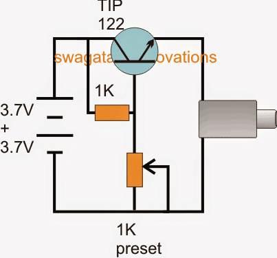 The first circuit above makes use of a common collector transistor configuration for charging the intended cellphone device, the 1K perset is initially adjusted to enable a precise 4.3V across the emitter of the transistor.
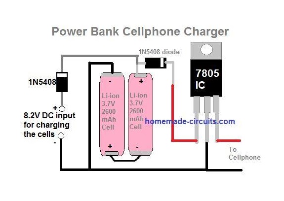 The second design above uses a 7805 voltage regulator circuit for implementing the power bank charging function
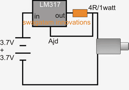 The last diagram here depicts a charger design using an LM317 current limiter.
This idea looks much impressive than the above two since it takes care of the voltage control and the current control together ensuring a prefect charging of the cellphone.
In all the four above power bank cell phone charger circuits, the charging of the two 3.7V cells can be done with the same TIP122 network which is discussed for the first boost charger design.
The 5V zener should be changed to a 9V zener diode and the charging input obtained from any standard 12V/1amp SMPS adapter.
The last diagram here depicts a charger design using an LM317 current limiter.
This idea looks much impressive than the above two since it takes care of the voltage control and the current control together ensuring a prefect charging of the cellphone.
In all the four above power bank cell phone charger circuits, the charging of the two 3.7V cells can be done with the same TIP122 network which is discussed for the first boost charger design.
The 5V zener should be changed to a 9V zener diode and the charging input obtained from any standard 12V/1amp SMPS adapter.
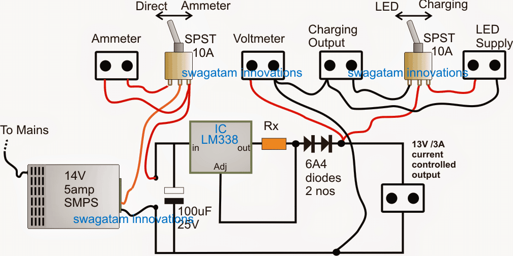 As shown in the above 12V LED backpack circuit diagram, the wiring and the circuit layout appears to be pretty straightforward, and with bare minimum components.
The details may be understood as given under:
The input supply is acquired from a ready made 14V/5amp SMPS unit, which can be seen at the extreme left side of the image.
If the user prefers to build the SMPS himself he may do so by referring to the diagram that's presented in the following article
12V, 5amp SMPS circuit
However procuring it ready made would be much easier and hassle free, and is recommended here.
As requested, the output from the SMPS can be seen passing through a changeover switch stage for enabling the option of a direct input to the load or through an ammeter depending upon the position of the SPST switch.
Next, the input supply is allowed to traverse through an LM338 IC stage configured as a current controller in order to manage the correct amount of amps to the load (LED modules), as well as for the charging of the battery.
The current limit is achieved by appropriately calculating the value of Rx.
The entire procedure for calculating the current limiter resistor may be learned from the following article:
Universal current limiter circuit
As indicated in the request, the current controlled 14V supply is terminated into a couple of pluggable sockets, one for enabling voltage measurement externally, while the remaining two facilitate the powering of the LEDs and the charging of the battery via another SPST switch.
The regulated 12V output from this 12v LED backpack power supply circuit can be seen connected with an extra separate socket so that the user is able to access the voltage for powering any other desired 12V gadget through the same.
As shown in the above 12V LED backpack circuit diagram, the wiring and the circuit layout appears to be pretty straightforward, and with bare minimum components.
The details may be understood as given under:
The input supply is acquired from a ready made 14V/5amp SMPS unit, which can be seen at the extreme left side of the image.
If the user prefers to build the SMPS himself he may do so by referring to the diagram that's presented in the following article
12V, 5amp SMPS circuit
However procuring it ready made would be much easier and hassle free, and is recommended here.
As requested, the output from the SMPS can be seen passing through a changeover switch stage for enabling the option of a direct input to the load or through an ammeter depending upon the position of the SPST switch.
Next, the input supply is allowed to traverse through an LM338 IC stage configured as a current controller in order to manage the correct amount of amps to the load (LED modules), as well as for the charging of the battery.
The current limit is achieved by appropriately calculating the value of Rx.
The entire procedure for calculating the current limiter resistor may be learned from the following article:
Universal current limiter circuit
As indicated in the request, the current controlled 14V supply is terminated into a couple of pluggable sockets, one for enabling voltage measurement externally, while the remaining two facilitate the powering of the LEDs and the charging of the battery via another SPST switch.
The regulated 12V output from this 12v LED backpack power supply circuit can be seen connected with an extra separate socket so that the user is able to access the voltage for powering any other desired 12V gadget through the same.
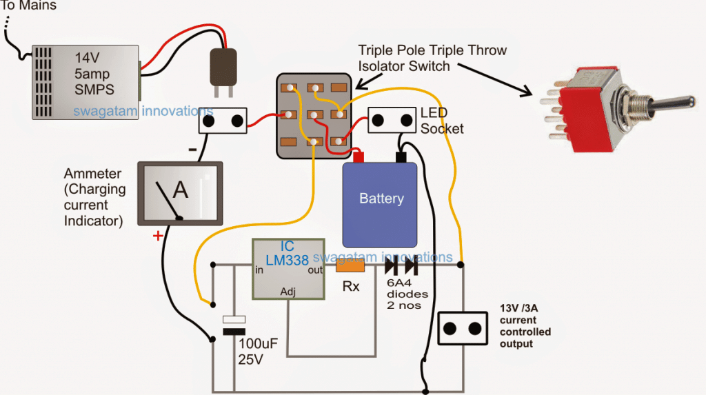 In the corrected diagram shown above, a single TPDT (3PDT) switch is employed and is able to achieve the intended charging of the battery as well as the illumination of the LED through a common LM338 current controller circuit.
So this idea enables both the charging of the battery and the illuminating of the LED to be implemented via a safely calculated current controlled supply, making the unit much compact and cost effective.
Rest of the section of the diagram are self evident.
Feedback from Mr.
Kevin
Hi Swag,
Just to say thank you for all your help with this project, I have just ordered all the bits I need to complete.
All the best
Kevin
In the corrected diagram shown above, a single TPDT (3PDT) switch is employed and is able to achieve the intended charging of the battery as well as the illumination of the LED through a common LM338 current controller circuit.
So this idea enables both the charging of the battery and the illuminating of the LED to be implemented via a safely calculated current controlled supply, making the unit much compact and cost effective.
Rest of the section of the diagram are self evident.
Feedback from Mr.
Kevin
Hi Swag,
Just to say thank you for all your help with this project, I have just ordered all the bits I need to complete.
All the best
Kevin
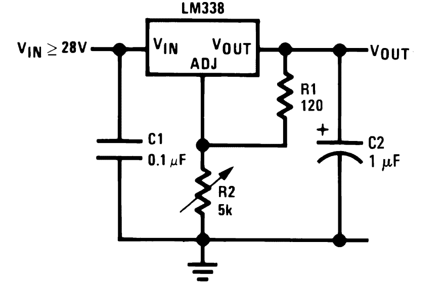 Varying the 5k pot enables setting of any desired constant voltage across the C2 capacitor (Vout) which can be used for charging a connected battery across these points.
For fixed voltage you could replace R2 with a fixed resistor, using this formula:
VO= VREF(1 + R2 / R1) + (IADJˇÁ R2)
Where VREFis = 1.25
Since IADJis too small it can be ignored
Although a constant voltage may be necessary, in places where the voltage from an input AC mains does not vary too much (a 5% up/down is quite acceptable) one may entirely eliminate the above circuit and forget about the constant voltage factor.
This implies that we can simply use a correctly rated transformer for charging a battery without considering a constant voltage condition, provided the mains input is fairly dependable in terms of its fluctuations.
Today with the advent of SMPS devices, the above issue completely becomes immaterial since SMPS are all constant voltage power supplies and are highly reliable with their specs, so if an SMPS is available, the above LM338 circuit can be definitely eliminated.
But commonly an SMPS comes with a fixed voltage, so in that case customizing it for a particular battery might become an issue and you may have to opt for the versatile LM338 circuit as explained above....
or if you still want to avoid this, you may simply modify the SMPS circuit itself for acquiring the desired charging voltage.
The following section will explain the designing of a customized current control circuit for a specific, selected battery charger unit.
Varying the 5k pot enables setting of any desired constant voltage across the C2 capacitor (Vout) which can be used for charging a connected battery across these points.
For fixed voltage you could replace R2 with a fixed resistor, using this formula:
VO= VREF(1 + R2 / R1) + (IADJˇÁ R2)
Where VREFis = 1.25
Since IADJis too small it can be ignored
Although a constant voltage may be necessary, in places where the voltage from an input AC mains does not vary too much (a 5% up/down is quite acceptable) one may entirely eliminate the above circuit and forget about the constant voltage factor.
This implies that we can simply use a correctly rated transformer for charging a battery without considering a constant voltage condition, provided the mains input is fairly dependable in terms of its fluctuations.
Today with the advent of SMPS devices, the above issue completely becomes immaterial since SMPS are all constant voltage power supplies and are highly reliable with their specs, so if an SMPS is available, the above LM338 circuit can be definitely eliminated.
But commonly an SMPS comes with a fixed voltage, so in that case customizing it for a particular battery might become an issue and you may have to opt for the versatile LM338 circuit as explained above....
or if you still want to avoid this, you may simply modify the SMPS circuit itself for acquiring the desired charging voltage.
The following section will explain the designing of a customized current control circuit for a specific, selected battery charger unit.
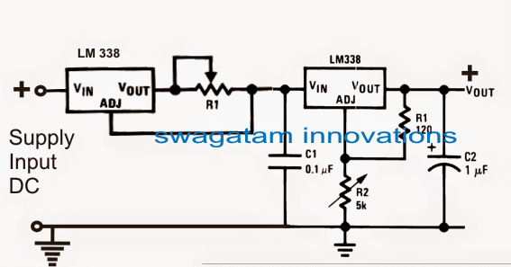 As discussed in the previous section, in case your input mains is fairly constant, then you can ignore the right hand side LM338 section, and simply use the left side current limiter circuit with either a transformer or an SMPS, as shown below:
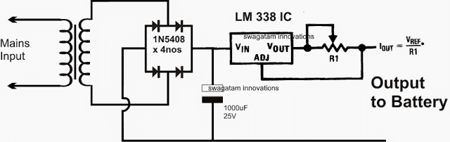 In the above design, the transformer voltage may be rated at the battery voltage level, but after rectification it might yield a little above the specified battery charging voltage.
This issue can be neglected because the attached current control feature will force the voltage to automatically sink the excess voltage to the safe battery charging voltage level.
R1 can be customized as per the needs, by following the instructions furnished HERE
The diodes must be appropriately rated depending on the charging current, and preferably should be much higher than the specified charging current level.
In the above design, the transformer voltage may be rated at the battery voltage level, but after rectification it might yield a little above the specified battery charging voltage.
This issue can be neglected because the attached current control feature will force the voltage to automatically sink the excess voltage to the safe battery charging voltage level.
R1 can be customized as per the needs, by following the instructions furnished HERE
The diodes must be appropriately rated depending on the charging current, and preferably should be much higher than the specified charging current level.
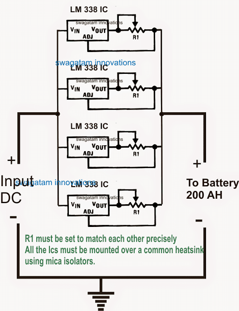 Any number of ICs may be added in the shown format for achieving any desired current limit, however two things must be ensured in order to get an optimal response from the design:
All the ICs must be mounted over a common heatsink, and all the current limiting resistors (R1) must be fixed with a precisely matching value, both the parameters are required to enable an uniform heat sharing among the ICs and hence equal current distribution across the output for the connected battery.
So far we have learned regarding how to customize constant voltage and constant current for a specific battery charger application.
However without an auto cut-off a battery charger circuit may be just incomplete and quite unsafe.
So far in our battery charging tutorials we learned how to customize constant voltage parameter while building a battery charger, in the following sections we will try to understand how to implement a full charge auto cut off for assuring a safe charging for the connected battery.
Any number of ICs may be added in the shown format for achieving any desired current limit, however two things must be ensured in order to get an optimal response from the design:
All the ICs must be mounted over a common heatsink, and all the current limiting resistors (R1) must be fixed with a precisely matching value, both the parameters are required to enable an uniform heat sharing among the ICs and hence equal current distribution across the output for the connected battery.
So far we have learned regarding how to customize constant voltage and constant current for a specific battery charger application.
However without an auto cut-off a battery charger circuit may be just incomplete and quite unsafe.
So far in our battery charging tutorials we learned how to customize constant voltage parameter while building a battery charger, in the following sections we will try to understand how to implement a full charge auto cut off for assuring a safe charging for the connected battery.
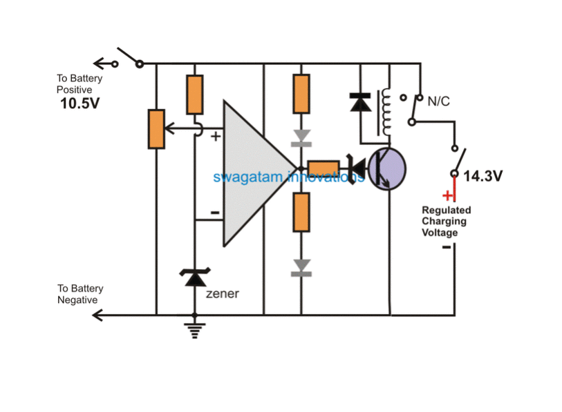 NOTE: Please use the relay N/O contact for the charging input, instead of the shown N/C.
This will ensure that the relay does not chatter in the absence of a battery. For this to work, also make sure to swap the input pins (2 and 3) with each other.
In the above simulation effect we can see that an opamp is been configured as a battery voltage sensor for detecting the over charge threshold, and cutting off the supply to the battery as soon as this is detected.
The preset at pin (+) of the IC is adjusted such that at full battery voltage (14.2V here), the pin#3 acquires a shade higher potential than the pin (-) of the IC which is fixed with a reference voltage of 4.7V with a zener diode.
The previously explained "constant voltage" and "constant current" supply is connected to the circuit, and the battery via the N/C contact of the relay.
Initially the supply voltage and the battery both are switched off from the circuit.
First, the discharged battery is allowed to be connected to the circuit, as soon as this is done, the opamp detects a potential that's lower (10.5V as assumed here) than the full charge level, and due to this the RED LED comes ON, indicating that the battery is below the full charge level.
Next, the 14.2V input charging supply is switched ON.
As soon as this is done, the input instantly sinks down to the battery voltage, and attains the 10.5V level.
The charging procedure now gets initiated and the battery begins getting charged.
As the battery terminal voltage increases in the course of the charging, the pin (+) voltage also correspondingly increases.
And the moment the battery voltage reaches the full input level that is the 14.3V level, the pin (+) also proportionately attains a 4.8V which is just higher than the pin (-) voltage.
This instantly forces the opamp output to go high.
The RED LED now switches OFF, and the green LED illuminates, indicating the changeover action and also that the battery is fully charged.
However what may happen after this is not shown in the above simulation.
We'll learn it through the following explanation:
As soon as the relay trips the battery terminal voltage will quickly tend to drop and restore to some lower level since a 12V battery will never hold a 14V level consistently and will try to attain a 12.8V mark approximately.
Now, due to this condition, the pin (+) voltage will again experience a drop below the reference level set by pin (-), which will yet again prompt the relay to switch OFF, and the charging process will be again initiated.
This ON/OFF toggling of the relay will keep on cycling making an undesirable "clicking" sound from the relay.
To avoid this it becomes imperative to add a hysteresis to the circuit.
This is done by introducing a high value resistor across the output and the (+) pin of the IC as shown below:
NOTE: Please use the relay N/O contact for the charging input, instead of the shown N/C.
This will ensure that the relay does not chatter in the absence of a battery. For this to work, also make sure to swap the input pins (2 and 3) with each other.
In the above simulation effect we can see that an opamp is been configured as a battery voltage sensor for detecting the over charge threshold, and cutting off the supply to the battery as soon as this is detected.
The preset at pin (+) of the IC is adjusted such that at full battery voltage (14.2V here), the pin#3 acquires a shade higher potential than the pin (-) of the IC which is fixed with a reference voltage of 4.7V with a zener diode.
The previously explained "constant voltage" and "constant current" supply is connected to the circuit, and the battery via the N/C contact of the relay.
Initially the supply voltage and the battery both are switched off from the circuit.
First, the discharged battery is allowed to be connected to the circuit, as soon as this is done, the opamp detects a potential that's lower (10.5V as assumed here) than the full charge level, and due to this the RED LED comes ON, indicating that the battery is below the full charge level.
Next, the 14.2V input charging supply is switched ON.
As soon as this is done, the input instantly sinks down to the battery voltage, and attains the 10.5V level.
The charging procedure now gets initiated and the battery begins getting charged.
As the battery terminal voltage increases in the course of the charging, the pin (+) voltage also correspondingly increases.
And the moment the battery voltage reaches the full input level that is the 14.3V level, the pin (+) also proportionately attains a 4.8V which is just higher than the pin (-) voltage.
This instantly forces the opamp output to go high.
The RED LED now switches OFF, and the green LED illuminates, indicating the changeover action and also that the battery is fully charged.
However what may happen after this is not shown in the above simulation.
We'll learn it through the following explanation:
As soon as the relay trips the battery terminal voltage will quickly tend to drop and restore to some lower level since a 12V battery will never hold a 14V level consistently and will try to attain a 12.8V mark approximately.
Now, due to this condition, the pin (+) voltage will again experience a drop below the reference level set by pin (-), which will yet again prompt the relay to switch OFF, and the charging process will be again initiated.
This ON/OFF toggling of the relay will keep on cycling making an undesirable "clicking" sound from the relay.
To avoid this it becomes imperative to add a hysteresis to the circuit.
This is done by introducing a high value resistor across the output and the (+) pin of the IC as shown below:
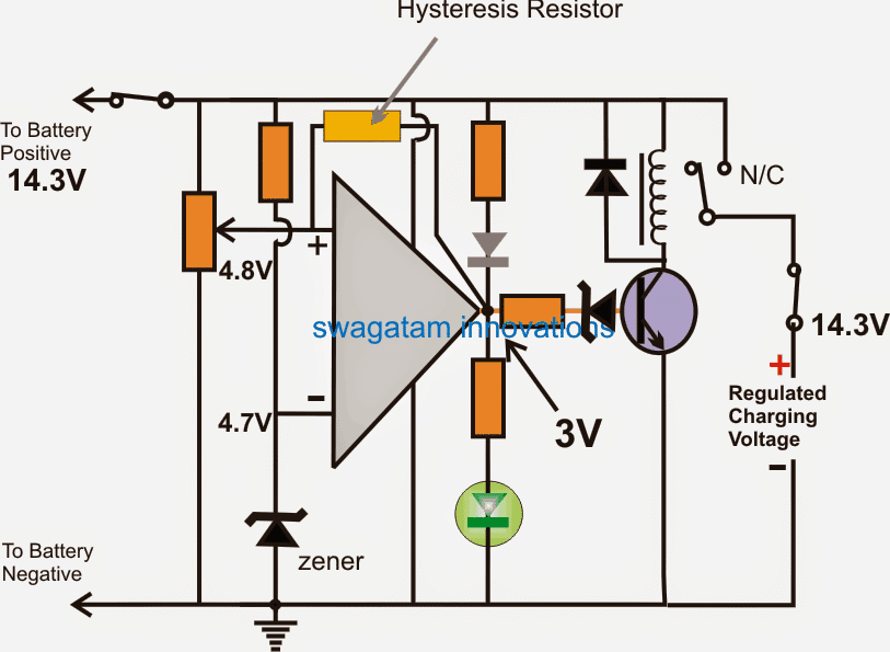
 A simple set up shown above can be universally used for charging any battery safely and quite optimally, provided you allow sufficient charging time or until you find the needle of the ammeter dropping down to almost zero.
 The 1000uf filter capacitor is actually not needed, as shown above, and eliminating it would actually enhance the battery life.
Have further doubts? Do not hesitate to express them through your comments.
Source:battery charging
The 1000uf filter capacitor is actually not needed, as shown above, and eliminating it would actually enhance the battery life.
Have further doubts? Do not hesitate to express them through your comments.
Source:battery charging
 We know that a 5V solar charger circuit can be easily built using linear ICs such as LM 317 or LM 338, you can find more info on this by reading the following articles:
Simple solar charger circuit
Simple current controlled charger circuit
However the biggest drawback with these linear battery chargers is the emission of heat through their body or through case dissipation, which results in wastage of precious power.
Due to this issue these IC are unable to produce a zero drop voltage output for the load and always require at least 3V higher inputs than the specified outputs.
The circuit of the 5V charger explained here is completely free from all these hassles, let's learn how an efficient working is achieved from the proposed circuit.
Referring to the above 5V PWM solar battery charger circuit, the IC TL494 forms the heart of the entire application.
The IC is a specialized PWM processor IC, which is used here for controlling a buck converter stage, responsible for converting the high input voltage into a preferred lower level output.
The input to the circuit can be anywhere between 10 and 40V, which becomes the ideal range for the solar panels.
The key features of the IC includes:
We know that a 5V solar charger circuit can be easily built using linear ICs such as LM 317 or LM 338, you can find more info on this by reading the following articles:
Simple solar charger circuit
Simple current controlled charger circuit
However the biggest drawback with these linear battery chargers is the emission of heat through their body or through case dissipation, which results in wastage of precious power.
Due to this issue these IC are unable to produce a zero drop voltage output for the load and always require at least 3V higher inputs than the specified outputs.
The circuit of the 5V charger explained here is completely free from all these hassles, let's learn how an efficient working is achieved from the proposed circuit.
Referring to the above 5V PWM solar battery charger circuit, the IC TL494 forms the heart of the entire application.
The IC is a specialized PWM processor IC, which is used here for controlling a buck converter stage, responsible for converting the high input voltage into a preferred lower level output.
The input to the circuit can be anywhere between 10 and 40V, which becomes the ideal range for the solar panels.
The key features of the IC includes:
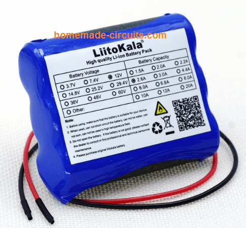
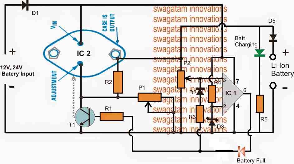

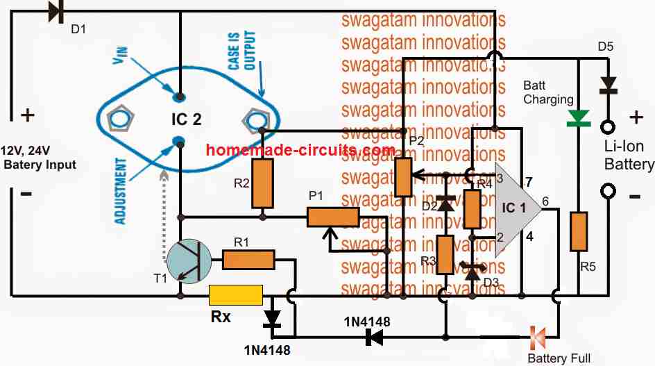 Note: The latching of the op amp is not compulsory, hence the D2 and R3 can be removed, and the circuit will still work nicely and automatically cut-off when the battery is fully charged.
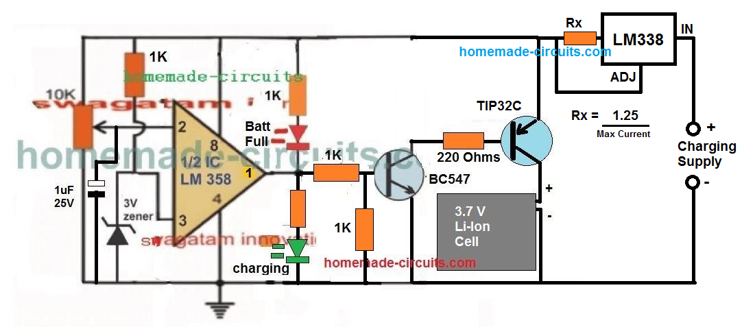 A 1uF capacitor is introduced at the inverting input of the IC, which ensures that the IC always starts with its output at positive high when powered.
This in turn allows a guaranteed switch ON of the output transistor, and enables the connected battery to lock in with the charging process.
The concept has been tested thoroughly, the video proof can be seen here.
WARNING: IN ALL THE ABOVE CONCEPTS, TEMPERATURE REGULATION FOR THE BATTERY IS NOT INCLUDED, SO PLEASE MAKE SURE TO ADJUST THE CURRENT TO A LEVEL WHICH DOES NOT CAUSE THE BATTERY TEMPERATURE TO REACH ABOVE 35 DEGREES CELSIUS.
A 1uF capacitor is introduced at the inverting input of the IC, which ensures that the IC always starts with its output at positive high when powered.
This in turn allows a guaranteed switch ON of the output transistor, and enables the connected battery to lock in with the charging process.
The concept has been tested thoroughly, the video proof can be seen here.
WARNING: IN ALL THE ABOVE CONCEPTS, TEMPERATURE REGULATION FOR THE BATTERY IS NOT INCLUDED, SO PLEASE MAKE SURE TO ADJUST THE CURRENT TO A LEVEL WHICH DOES NOT CAUSE THE BATTERY TEMPERATURE TO REACH ABOVE 35 DEGREES CELSIUS.
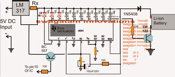 When power is switched ON, the 100uF/25V capacitor across the pin5 preset of the IC momentarily grounds pin5 so that all the outputs of the IC begin by staying shut off.
This is important to make sure that the TIP122 is able to initiate the charging process and the BC557 is inhibited from an accidental switch ON due to the initial surge transients.
As soon as the 100uF is charged up, pin5 is allowed to sense the actual voltage that's been utilized by the battery while it's been charged, which should be normally anywhere around 3 to 3.3V for a fully discharged 3.7V Li-ion battery.
Here each LED may be set to indicate an increment of 0.42V, which implies that the illumination of the 10th LED indicates 4.2V which may be assumed to be the battery full charge level indication.
This also implies that during power ON, 7 LEDs must be illuminated to indicate a correct battery discharge level and charging process.
Less that 7 LEDs illuminated would indicate a badly discharged battery or a damaged battery consuming excess current than the specified range.
With all the LEDs lighting up during power switch ON would imply either the battery is fully charged or the battery is not accepting charge and is faulty.
Under normal conditions, around 7/8 LEDs should be illuminated at power switch ON and as the battery voltage increases due to charging, the LEDs should also sequence by illuminating the 8th, 9th and the 10th LED sequentially.
Once the 10th LED is illuminated, a low logic is sent to the base of the TIP122 which is now inhibited from a base bias and the charging voltage to the battery is thus cut off, switching off the charging voltage to the battery.
The low logic from the 10th pin is also sent to the base of the shown BC557 which conducts and connects pin5 of the IC directly to the 5V supply making sure that the 10th LED becomes latched and the situation is locked until power is switched OFF and ON for further actions.
When power is switched ON, the 100uF/25V capacitor across the pin5 preset of the IC momentarily grounds pin5 so that all the outputs of the IC begin by staying shut off.
This is important to make sure that the TIP122 is able to initiate the charging process and the BC557 is inhibited from an accidental switch ON due to the initial surge transients.
As soon as the 100uF is charged up, pin5 is allowed to sense the actual voltage that's been utilized by the battery while it's been charged, which should be normally anywhere around 3 to 3.3V for a fully discharged 3.7V Li-ion battery.
Here each LED may be set to indicate an increment of 0.42V, which implies that the illumination of the 10th LED indicates 4.2V which may be assumed to be the battery full charge level indication.
This also implies that during power ON, 7 LEDs must be illuminated to indicate a correct battery discharge level and charging process.
Less that 7 LEDs illuminated would indicate a badly discharged battery or a damaged battery consuming excess current than the specified range.
With all the LEDs lighting up during power switch ON would imply either the battery is fully charged or the battery is not accepting charge and is faulty.
Under normal conditions, around 7/8 LEDs should be illuminated at power switch ON and as the battery voltage increases due to charging, the LEDs should also sequence by illuminating the 8th, 9th and the 10th LED sequentially.
Once the 10th LED is illuminated, a low logic is sent to the base of the TIP122 which is now inhibited from a base bias and the charging voltage to the battery is thus cut off, switching off the charging voltage to the battery.
The low logic from the 10th pin is also sent to the base of the shown BC557 which conducts and connects pin5 of the IC directly to the 5V supply making sure that the 10th LED becomes latched and the situation is locked until power is switched OFF and ON for further actions.
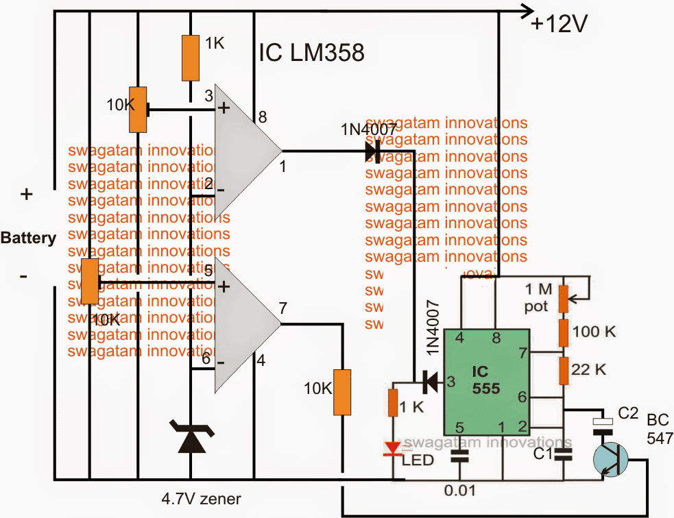 Initially both the opamp outputs may be assumed to be low, if the battery is discharged below 11V, this will be indicated with a fast blinking of the LED.
C1 must be set for achieving this fast blinking.
The lower opamps is set using pin5 preset such that when the connected 12V battery reaches around 12.5V, its output pin goes high, once this happens the BC547 triggers and adds a high value capacitor C2 in parallel with C1 slowing down the flashing rate significantly and indicating that the battery has entered the next upper charging phase and also that the battery is good and is accepting the charge well.
As the battery continues to get charged and acquires a voltage level of around 14V, the upper opamp which is set using pin3 preset to trigger at this point triggers and renders a high across the connected LED stopping its flashing and illuminating it to solid.
Once this happens the user may assume the battery to have reached the optimal charging level and may remove it from the charger.
Initially both the opamp outputs may be assumed to be low, if the battery is discharged below 11V, this will be indicated with a fast blinking of the LED.
C1 must be set for achieving this fast blinking.
The lower opamps is set using pin5 preset such that when the connected 12V battery reaches around 12.5V, its output pin goes high, once this happens the BC547 triggers and adds a high value capacitor C2 in parallel with C1 slowing down the flashing rate significantly and indicating that the battery has entered the next upper charging phase and also that the battery is good and is accepting the charge well.
As the battery continues to get charged and acquires a voltage level of around 14V, the upper opamp which is set using pin3 preset to trigger at this point triggers and renders a high across the connected LED stopping its flashing and illuminating it to solid.
Once this happens the user may assume the battery to have reached the optimal charging level and may remove it from the charger.
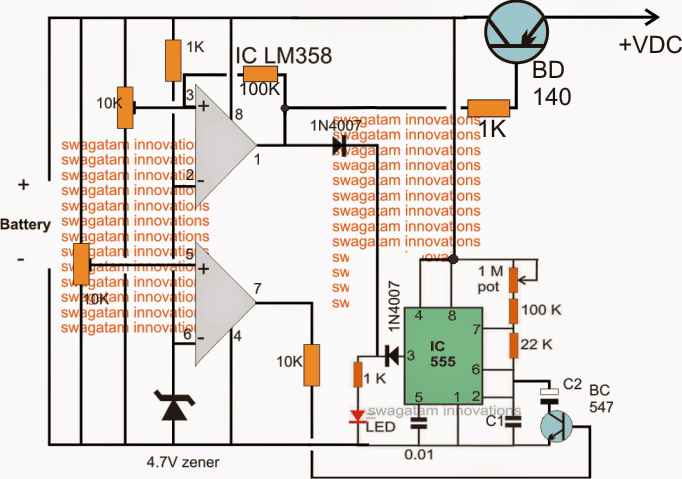 While setting up the two presets make sure the 100K link remains disconnected in the upper opamp.
After setting up the thresholds, the 100k link can be reconnected into position.
The circuit will not initiate until a battery is connected, so make sure the battery to be charged is first connected and then power is switched ON.
For a 3.7V battery, the 4.7V zener must be replaced with two
A little in-depth investigation shows that in the above circuit C2 will not have a discharge path through the connected BC547 and therefore it won't help to slow down the oscillations while the lower opamp is in the activated state.
The correct implementation of the above concept could probably be done by using an optocoupler as shown in the following figure.
Here instead of targeting the frequency determining capacitor C2 the resistor counterpart is selected for the intended control of the frequency and LED blinking rate:
While setting up the two presets make sure the 100K link remains disconnected in the upper opamp.
After setting up the thresholds, the 100k link can be reconnected into position.
The circuit will not initiate until a battery is connected, so make sure the battery to be charged is first connected and then power is switched ON.
For a 3.7V battery, the 4.7V zener must be replaced with two
A little in-depth investigation shows that in the above circuit C2 will not have a discharge path through the connected BC547 and therefore it won't help to slow down the oscillations while the lower opamp is in the activated state.
The correct implementation of the above concept could probably be done by using an optocoupler as shown in the following figure.
Here instead of targeting the frequency determining capacitor C2 the resistor counterpart is selected for the intended control of the frequency and LED blinking rate:
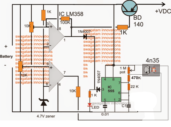 Now it looks much better.
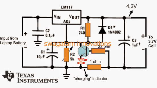 The value of R2 could be calculated either through this calculator software or using the following formula:
VO= VREF(1 + R2 / R1) + (IADJˇÁ R2)
where VREF = 1.25
The IADJcould be eliminated since it's too small to be considered in most cases.
The value of R2 could be calculated either through this calculator software or using the following formula:
VO= VREF(1 + R2 / R1) + (IADJˇÁ R2)
where VREF = 1.25
The IADJcould be eliminated since it's too small to be considered in most cases.
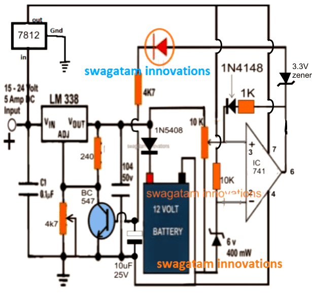
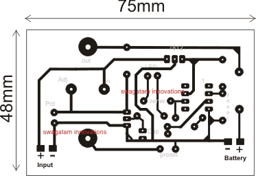
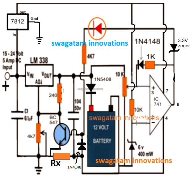 As can be seen, a simple addition of a current limiting resistor and a diode link transforms the design into an effective CC or constant current Lipo cell charger.
Now when the output tries to draw current above the specified CC limit, a calculated potential is developed across Rx, which passes through the 1N4148 diode triggering the BC547 base, which in turn conducts and grounds the ADJ pin of the IC LM338, forcing the IC to switch OFF the supply to charger.
Rx may be calculated with the following formula:
Rx = Forward voltage limit of BC547 and 1N41448 / Max battery current limit
Therefore Rx = 0.6 + 0.6 / Max battery current limit
As can be seen, a simple addition of a current limiting resistor and a diode link transforms the design into an effective CC or constant current Lipo cell charger.
Now when the output tries to draw current above the specified CC limit, a calculated potential is developed across Rx, which passes through the 1N4148 diode triggering the BC547 base, which in turn conducts and grounds the ADJ pin of the IC LM338, forcing the IC to switch OFF the supply to charger.
Rx may be calculated with the following formula:
Rx = Forward voltage limit of BC547 and 1N41448 / Max battery current limit
Therefore Rx = 0.6 + 0.6 / Max battery current limit
 Diagram

 FOR IMPROVING ACCURACY PLEASE REMOVE THE RED LED FROM THE EXISTING POSITION AND CONNECT IT IN SERIES WITH THE BC547 BASE.
ALSO, NOW YOU CAN ELIMINATE THE PIN6 ZENER DIODE.
The operations involved with the first diagram above gets much simplified if a relay stage used instead of BJTs, and mosfets.
As can be seen in the above updated diagram, the relay stage is in the form of two 24V relays in series, wherein the coils are joined in series while the contacts are joined in parallel.
The sensing circuit is applied with a proportionately scaled down voltage through an emitter follower voltage divider circuit using the indicated BC546 stage for the intended battery level detection and cut-offs
The following diagram shows an extremely simple 48 V solar charger system which allows the load to access the solar panel power during day time when there's optimal sunshine, and features an automatic switch over to battery mode during night when the solar voltage is unavailable:
FOR IMPROVING ACCURACY PLEASE REMOVE THE RED LED FROM THE EXISTING POSITION AND CONNECT IT IN SERIES WITH THE BC547 BASE.
ALSO, NOW YOU CAN ELIMINATE THE PIN6 ZENER DIODE.
The operations involved with the first diagram above gets much simplified if a relay stage used instead of BJTs, and mosfets.
As can be seen in the above updated diagram, the relay stage is in the form of two 24V relays in series, wherein the coils are joined in series while the contacts are joined in parallel.
The sensing circuit is applied with a proportionately scaled down voltage through an emitter follower voltage divider circuit using the indicated BC546 stage for the intended battery level detection and cut-offs
The following diagram shows an extremely simple 48 V solar charger system which allows the load to access the solar panel power during day time when there's optimal sunshine, and features an automatic switch over to battery mode during night when the solar voltage is unavailable:
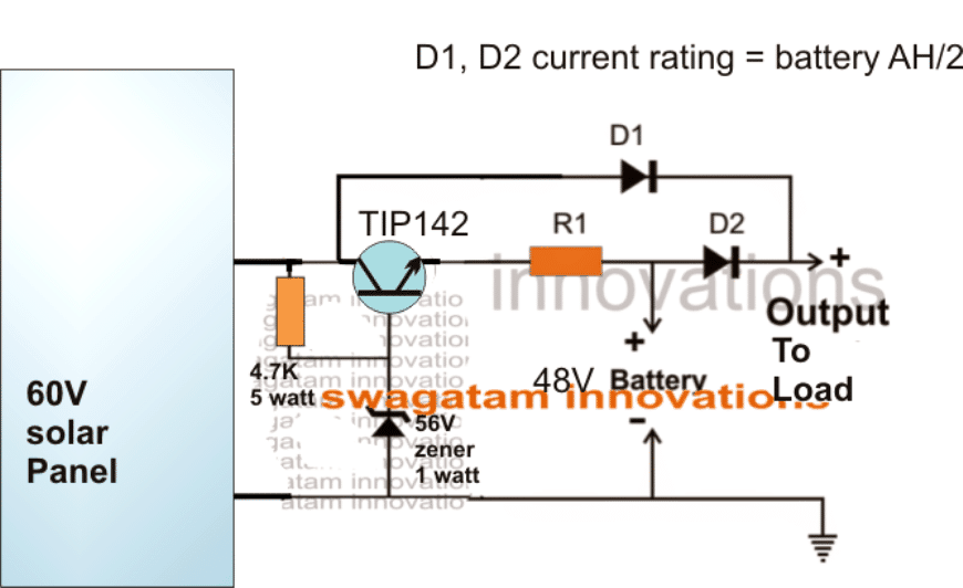
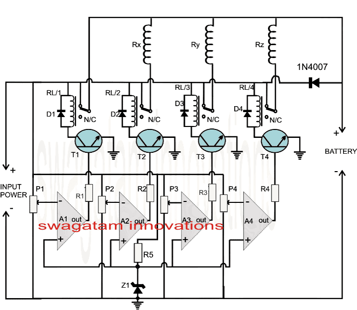 PLEASE CONNECT AN LED IN SERIES WITH R1, R2, R3, R4, EACH IN ORDER TO GET A SYNCHRONOUS READING OF THE CHARGING STATUS OF THE BATTERY.
INITIALLY ALL THE LEDS WILL BE ON INDICATING MAXIMUM CURRENT, THEN SUBSEQUENTLY THE LEDS WILL SWITCH OFF ONE BY ONE UNTIL ONLY A4 LED REMAINS ON INDICATING FLOAT CHARGING, AND THE BATTERY FULLY CHARGED.
The IC LM324 is quad opamp IC whose all the four opamps are used for the intended sequential switching of the output current levels.
The proceedings are very easy to understand.
opamps A1 to A2 are optimized for switching at different voltage levels during the course of the stepped charging of the connected battery.
All the non-inverting inputs of the opamps are referenced to ground through the zener voltage.
The inverting inputs are tied with the positive supply of the circuit via the corresponding presets.
If we assume the battery to be a 12V battery having a discharge level of 11V, P1 may be set such that the relay just disconnects when the battery voltage reaches 12V, P2 may be adjusted to release the relay at 12.5V, P3 may be done for te same at 13.5V and finally P4 could be set for responding at the battery full charge level of 14.3V.
Rx, Ry, Rz have same values and are optimized to provide the battery with the required amount of current during the various charging voltage levels.
The value could be fixed such that each inductor allows a current passage rate that may be 1/10th of the battery AH.
It may be determined by using ohms law:
R = I/V
The values of Rx, alone or Rx, Ry together could be dimensioned a little differently for allowing relatively more current to the battery during the initial stages as per individual preferences, and is tweakable.
PLEASE CONNECT AN LED IN SERIES WITH R1, R2, R3, R4, EACH IN ORDER TO GET A SYNCHRONOUS READING OF THE CHARGING STATUS OF THE BATTERY.
INITIALLY ALL THE LEDS WILL BE ON INDICATING MAXIMUM CURRENT, THEN SUBSEQUENTLY THE LEDS WILL SWITCH OFF ONE BY ONE UNTIL ONLY A4 LED REMAINS ON INDICATING FLOAT CHARGING, AND THE BATTERY FULLY CHARGED.
The IC LM324 is quad opamp IC whose all the four opamps are used for the intended sequential switching of the output current levels.
The proceedings are very easy to understand.
opamps A1 to A2 are optimized for switching at different voltage levels during the course of the stepped charging of the connected battery.
All the non-inverting inputs of the opamps are referenced to ground through the zener voltage.
The inverting inputs are tied with the positive supply of the circuit via the corresponding presets.
If we assume the battery to be a 12V battery having a discharge level of 11V, P1 may be set such that the relay just disconnects when the battery voltage reaches 12V, P2 may be adjusted to release the relay at 12.5V, P3 may be done for te same at 13.5V and finally P4 could be set for responding at the battery full charge level of 14.3V.
Rx, Ry, Rz have same values and are optimized to provide the battery with the required amount of current during the various charging voltage levels.
The value could be fixed such that each inductor allows a current passage rate that may be 1/10th of the battery AH.
It may be determined by using ohms law:
R = I/V
The values of Rx, alone or Rx, Ry together could be dimensioned a little differently for allowing relatively more current to the battery during the initial stages as per individual preferences, and is tweakable.
 This the original size PCB layout, from the track side, the high watt resistors are not included in the PCB design.
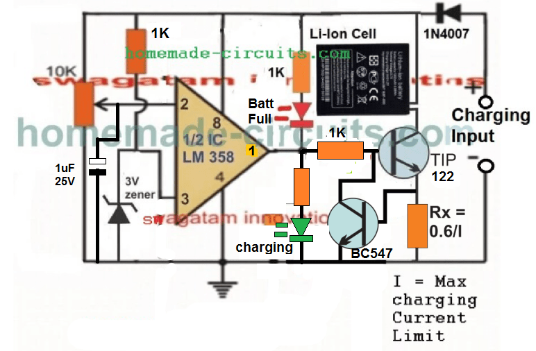 Since the current from a computer USB can be quite less, the current control stage can be ignored and the above design can be much simplified as shown below:
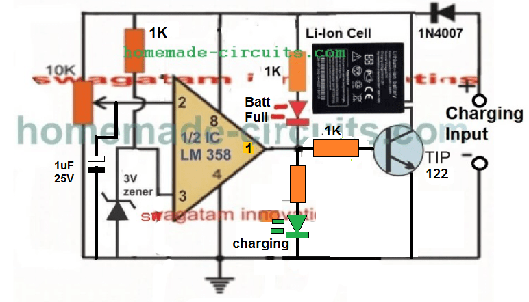 Video Clip showing the automatic cut off action, when the Li-Ion cell is charged upto 4.11V:
Please note that the circuit will not initiate charging unless a battery is connected prior to power switch ON, therefore please connect the battery first before connecting it to the USB port
An LM358 has two opamps which means one opamp is wasted here and remains unused, therefore LM321 may be tried instead to avoid the presence of an idle unused opamp.
Video Clip showing the automatic cut off action, when the Li-Ion cell is charged upto 4.11V:
Please note that the circuit will not initiate charging unless a battery is connected prior to power switch ON, therefore please connect the battery first before connecting it to the USB port
An LM358 has two opamps which means one opamp is wasted here and remains unused, therefore LM321 may be tried instead to avoid the presence of an idle unused opamp.
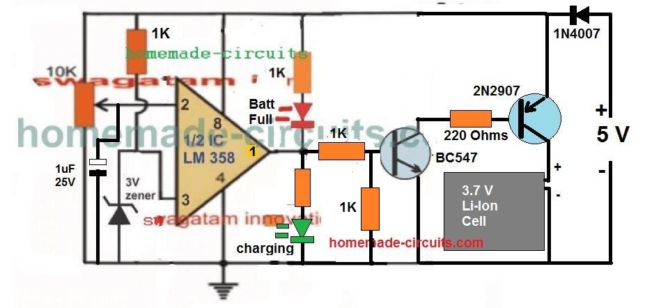 This design improved the current delivery significantly, and resulted in a reduction in the margin of difference between the battery terminal voltage level and the actual supply voltage level, and therefore false cut-off switching.
The following video, shows the test result using the above circuit:
Using a 5V Relay
The above designs can be also built using a 5V, which will ensure the best possible current delivery to the cell and faster charging.
The circuit diagram can be seen below:
This design improved the current delivery significantly, and resulted in a reduction in the margin of difference between the battery terminal voltage level and the actual supply voltage level, and therefore false cut-off switching.
The following video, shows the test result using the above circuit:
Using a 5V Relay
The above designs can be also built using a 5V, which will ensure the best possible current delivery to the cell and faster charging.
The circuit diagram can be seen below:
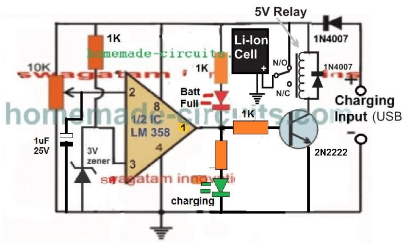 Please Note:
This article was substantially changed recently and therefore the older comment discussions may not match with the circuit diagram shown in this present updated design and explanation.
Please Note:
This article was substantially changed recently and therefore the older comment discussions may not match with the circuit diagram shown in this present updated design and explanation.
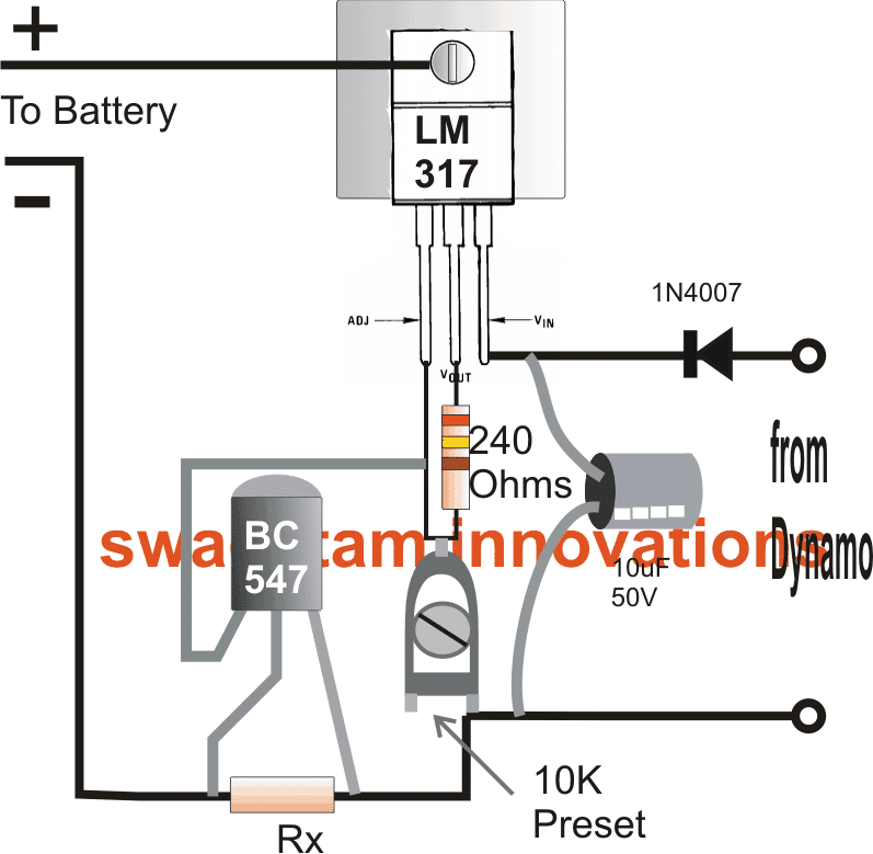
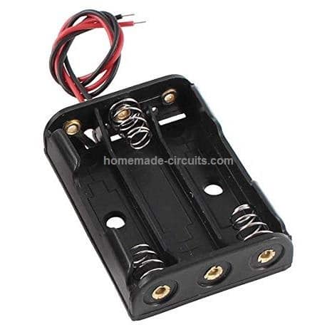
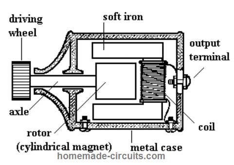 It is basically a 6V dynamo, with a maximum current capacity of 500mA.
Even at a slow bicycle speed of 5 km/hour, this type of dynamo will produce a decent output of 6V @ 100mA.
This power could be used for charging an Ni-Cd or N-Mh cells or even a Li-Ion cell.
Li-Ion cell might take a long time to charge at this rate, unless a buck converter is employed.
It is basically a 6V dynamo, with a maximum current capacity of 500mA.
Even at a slow bicycle speed of 5 km/hour, this type of dynamo will produce a decent output of 6V @ 100mA.
This power could be used for charging an Ni-Cd or N-Mh cells or even a Li-Ion cell.
Li-Ion cell might take a long time to charge at this rate, unless a buck converter is employed.
 The cell specifications could be as indicated below:

 The connections look pretty simple.
You will need a soldering iron and solder wire for joining the shown parameters.
Begin by making the bridge rectifier using 1N4007 diodes, as explained in this article.
Next, insert and fix the cells in the battery box.
After this, install the dynamo on the bicycle frame.
Finally, join the ends of the shown components using flexible wires with one another.
Be sure to connect the ammeter with correct +/- polarity, otherwise the meter needle will deflect towards the left side instead of right side.
(+) of the meter will go to the 10 ohm resistor.
Warning: Since the dynamo body acts like one of the output terminals, make sure it does not come in contact with any of the wire connections of the circuit, except the point where the lower orange wire is hooked up.
In short, keep the diode side circuit secured inside a plastic box.
The connections look pretty simple.
You will need a soldering iron and solder wire for joining the shown parameters.
Begin by making the bridge rectifier using 1N4007 diodes, as explained in this article.
Next, insert and fix the cells in the battery box.
After this, install the dynamo on the bicycle frame.
Finally, join the ends of the shown components using flexible wires with one another.
Be sure to connect the ammeter with correct +/- polarity, otherwise the meter needle will deflect towards the left side instead of right side.
(+) of the meter will go to the 10 ohm resistor.
Warning: Since the dynamo body acts like one of the output terminals, make sure it does not come in contact with any of the wire connections of the circuit, except the point where the lower orange wire is hooked up.
In short, keep the diode side circuit secured inside a plastic box.
 Note: Connect the emitters of T1/T2 to ground through 1N4148 diodes, this is important otherwise the opamp3/4 outputs won't be able to switch OFF the BJTs correctly.
As we can see in the above automatic double battery charger with isolator circuit, the relay N/O contacts are responsible for the required charging of the connected relevant batteries.
Since these batteries need to be charged with an "intelligent" charger, the system should be a step-charger kind of unit.
One such circuit has been discussed in this 3 step battery charger circuit, which may effectively employed here for the proposed method of charging both the batteries.
Note: Connect the emitters of T1/T2 to ground through 1N4148 diodes, this is important otherwise the opamp3/4 outputs won't be able to switch OFF the BJTs correctly.
As we can see in the above automatic double battery charger with isolator circuit, the relay N/O contacts are responsible for the required charging of the connected relevant batteries.
Since these batteries need to be charged with an "intelligent" charger, the system should be a step-charger kind of unit.
One such circuit has been discussed in this 3 step battery charger circuit, which may effectively employed here for the proposed method of charging both the batteries.