IC 555 Pinouts, Astable, Monostable, Bistable Circuits, Formulas
The post explains the how IC 555 works, its basic pinout details and how to configure the IC in its standard or popular astable, bistable, and monostable circuit modes.
The post also details the various formulas for calculating the IC 555 parameters.
Introduction
Our hobby world would be less interesting without IC 555. It would be one of our first IC to use in electronics.
In this article we are going to look back at history of IC555, their 3 operating modes and some of their specifications.
IC 555 was introduced in 1971 by a company called ¡°Signetics¡±; it was designed by Hans R.
Camenzind.
It is estimated that about 1 billion IC 555s are manufactured every year.
That¡¯s one IC 555 for every 7 people in the world.
The Signetics Company is owned by Philips Semiconductor.
If we look at the internal block diagram of IC 555 we find three 5K ohm resistors connected in series for deciding the timing factor, so probably that's how the device got its name IC 555 timer.
However, some hypothesis claims that the selection of the name has no relation to the internal components of the IC, it was arbitrarily selected.
How IC 555 Works
A standard IC555 consist of 25 transistors, 15 resistors and 2 diodes integrated on a silicon die.
There are two versions of the IC available namely military and civilian grade 555 timer.
The NE555 is a civilian grade IC and has operating temperature range of 0 to +70 degree Celsius.
The SE555 is military grade IC and has operating temperature range of -55 to +125 degree Celsius.
You will also find the CMOS version of timer known as 7555 and TLC555; these consume less power compared to standard 555 and operate less than 5V.
CMOS version timers consist of MOSFETs rather than bipolar transistor, which is efficient and consume less power.
IC 555 Pinout and Working Details:
Pin 1: Ground or 0V: It's the negative supply pin of the IC
Pin 2: Trigger or input: A negative momentary trigger on this input pin causes the output pin3 to go HIGH.
This happens by a quick discharging of the timing capacitor below the lower threshold level of 1/3rd supply voltage.
The capacitor then slowly charges via the timing resistor, and when it rises above 2/3rd supply level, pin3 become LOW again.
This ON/OFF switching is done by an internal FLIP-FLOP stage.
Pin 3: Output: It's the output which responds to the input pins either by going high or low, or by oscillating ON/OFF
Pin 4: Reset: It's the reset pin which is always connected to the positive supply for normal working of the IC.
When grounded momentarily resets the IC output to its initial position, and if permanently connected to ground keeps the IC operations disabled.
Pin 5: Control: An external variable DC potential can be applied on this pin to control or modulate the pin3 pulse width, and generate a controlled PWM.
Pin 6: Threshold: This is the threshold pin which causes the output to go LOW (0V) as soon as the timing capacitor charge reaches the upper threshold of 2/3rd supply voltage.
Pin 7: Discharge: This is the discharge pin controlled by the internal flip flop, which forces the timing capacitor to discharge as soon as it has reached the 2/3rd supply voltage threshold level.
Pin 8: Vcc: It's the positive supply input between 5 V and 15 V.
3 Modes of timer:
Bistable or Schmitt trigger
Monostable or one shot
Astable
Bistable Mode:
When the IC555 is configured in bistable mode it works as a basic flip-flop.
In other words when the input trigger is given, it toggles the output stateON or OFF.
Normally #pin2 and #pin4 are connected to pull-up resistors in this mode of operation.
When the #pin2 is grounded for short duration, the output at #pin3 goes high; to reset the output, #pin4 is momentarily shorted to ground, and then the output goes low.
There is no need for a timing capacitor here, but connecting a capacitor (0.01uF to 0.1uF) across #pin5 and ground is recommended.
#pin7 and #pin6 can be left unconnected in this configuration.
Here is a simple bistable circuit:
When the set button is depressed the output goes high and when reset button is depressed the output goes to low state.
R1 and R2 may be 10k ohm, the capacitor may be anywhere between the specified value.
Monostable Mode:
Another useful application of the IC 555 timer is in the form of a one-shot or monostable multivibrator circuit, as shown in the figure below.
As soon as the input trigger signal becomes negative, the one-shot mode is activated, causing the output pin 3 to go high at the Vcc level.
The time period of the output high condition can be calculated suing the formula:
Thigh = 1.1 RAC
As seen in the figure, the
negative edge of the input forces the comparator 2 to toggle the flip-flop.
This action causes the output at pin 3 to go high.
Actually in this process the capacitor C is charged toward VCC via the resistor RA.
While the capacitor charges, the output is held high at the Vcc level.
Video Demo
When the voltage across the capacitor acquires the threshold level of 2VCC/3, comparator 1 triggers the flip-flop, forcing the output to change state and go low.
This subsequently turns the discharge low, causing the capacitor to discharge and maintain at around 0 V until the next input trigger.
The figure above shows the entire procedure when the input is triggered low, leading to an output waveform for a monostable one shot action of the IC 555.
The timing of the output for this
mode can range from microseconds to many seconds, allowing this operation to
become ideally useful for a range of different applications.
Simplified Explanation for the Newbies
Monostable or one-shot pulse generators are widely used in many electronic applications, where a circuit needs to be switched ON for pre-determined time after a trigger.
The output pulse width at #pin3 can be determined by using this simple formula:
T = 1.1RC
Where
T is the time in Seconds
R is resistance in ohm
C is capacitance in farads
The output pulse falls when the voltage across the capacitor equals to 2/3 of the Vcc.
The input trigger between two pulses must be greater than RC time constant.
Here is a simple Monostable circuit:
Solving a Practical Monostable Application
Find out the period of the output waveform for the circuit example shown below when it is triggered by a negative edge pulse.
Solution:
Thigh = 1.1 RAC = 1.1(7.5 x 10³)(0.1 x 10⁻⁶) = 0.825 ms
How Astable Mode Works:
Referring to the IC555 astable circuit figure below, the Capacitor C is charged towards VCC level through the two resistors RA and RB.
The capacitor is charged until it reaches above 2VCC/3. This voltage becomes the threshold voltage on pin 6 of the IC.
This voltage operates comparator 1 to trigger the flip-flop, which causes the output at pin 3 to become low.
Along with this, the discharge transistor is switched ON, resulting in the pin 7 output discharging the capacitor via resistor RB.
This causes the voltage inside the capacitor to fall until finally it drops below the trigger level (VCC/3).
This action instantly triggers the flip flop stage of the IC, causing the output of the IC to go become high, turning OFF the discharge transistor.
This yet again enables the capacitor to get charged via resistors RA and RB toward VCC.
The time intervals
which is responsible for turning the output high and low can be calculated using
the relations
Thigh ¡Ö 0.7(RA + RB)C
Tlow ¡Ö 0.7 RBC
The total period is
T = period = Thigh + Tlow
Video Tutorial
Simplified Explanation for the Newbies
This is the most commonly used multivibrator or AMV designs such as in oscillators, sirens, alarms, flashers etc, and this would be one of our first circuit implemented for IC 555 as a hobbyist (remember alternate blinker LED?).
When IC555 configured as astable multivibrator, it gives out continuous rectangular shaped pulses at #pin3.
The frequency and pulse width can be regulated by R1, R2 and C1.The R1 is connected between Vcc and discharge #pin7, R2 is connected between #pin7 and #pin2 and also #pin6. The #pin6 and #pin2 are shorted.
The capacitor is connected between #pin2 and ground.
The frequency for Astable multivibrator can be Calculated by using this formula:
F = 1.44/((R1+R2*2)*C1)
Where,
F is the frequency in Hertz
R1 and R2 is resistors in ohms
C1 is capacitor in farads.
The high time for each pulse given by:
High= 0.693(R1+R2)*C
Low time is given by:
Low= 0.693*R2*C
All ¡®R¡¯ is in ohms and ¡®C¡¯ is in ohms.
Here is a basic astable multivibrator circuit:
For 555 IC timers with bipolar transistors, R1 with low value must be avoided so that the output stays saturated near ground voltage during discharge process, else the ¡®low time¡¯ could be unreliable and we may see greater values for low time practically than calculated value.
Solving an Astable Example Problem
In the following figure find the frequency of the IC 555 and draw the output waveform results.
Solution:
Waveform images can be seen below:
IC 555 PWM Circuit using Diodes
If you want the output less than 50% duty cycle i.e.
shorter high time and longer low time, a diode can be connected across R2 with cathode on the capacitor side.
It's also called the PWM mode for the 555 IC timer.
You can also design a 555 PWM circuit with variable duty cycle two diodes as shown in the above figure.
The PWM IC 555 circuit using two diodes is basically an astable circuit where the charge and discharge timing of the capacitor C1 is bifurcated through separate channels using diodes.
This modification enables the user to adjust the ON/OFF periods of the IC separately, and therefore achieve the desired PWM rate quickly.
Calculating PWM
In a IC 555 circuit using two diodes, the formula for calculating the PWM rate can be achieved using the following formula:
Thigh ¡Ö 0.7(R1 + POT Resistance)C
Here, POT resistance refer to the potentiometer adjustment, and the resistance level of that particular side of the pot through which the capacitor C charges.
Let's say the pot is a 5 K pot, and it's adjusted at 60/40 level, producing resistance levels of 3 K and 2 K.
Then depending on which portion of the resistance is charging the capacitor, the value could be used in the above formula.
If it's the 3 K side adjustment that is charging the capacitor, then the formula could be solved as:
Thigh ¡Ö 0.7(R1 + 3000 ¦¸) C
On the other hand, if it's 2 K that's on the charging side of the pot adjustment, then the formula may be solved as.
Thigh ¡Ö 0.7(R1 + 2000¦¸) C
Please remember, in both cases the C will be in Farads.
So you must first convert the microfarad value in your schematic into Farad, for getting a correct solution.
IC 555 Pulse Generator
This IC 555 circuit might seem recognizable to a lot of visitors because it is among the several versions of circuits from the common 555 timer circuits.
That does not essentially reduce its usefulness though.
Simply because, a flexible pulse generator having a adjustable duty cycle can be a very handy equipment for any electronic workshop.
In contrast to the conventional 555 astable circuits that are generally implemented, the resistors between pins 6 and 7 includes P1, P2, R2, DI and D2.
A tightly characterized charging time for capacitor C1 is established by the diodes D1 and D2.
This typically results in the duty cycle of around 50%, if it weren't for P2. For the present scenario the duty cycle is determined by the relationship between P1 and P2: n = 1 + P2/P1. For instance, if P2 = 0 (n = 100%), the frequency will then be:
f = 0.69 / [2(P1+P2+4.7k¦¸)C1
References: Stackexchange
Make this SleepWalk Alert ¨C Protect yourself from Sleepwalking Dangers
Do you have a habit of walking in night? Well, that habit isn¡¯t that good, so one must try to get rid of it gradually.
This article discusses a simple sleep walk alert circuit that might help you in getting out of this habit.
By: SS Kopparthy
Circuit Objective
This circuit is a simple idea of warning a person who is using this when they try to get down the bed by vibrating an small DC vibration motor attached to the person¡¯s leg so that the person can be awakened due to vibrations and can get back to bed.
The sensor used to detect that person is out of bed is a pressure sensor that is home made using two square copper clad strips of side 6.5cm and a sponge of 2.5cm width placed between the copper strips.
This arrangement acts as a variable capacitor and the capacitance changes when the pressure applied on it changes and this is used to trigger IC 555 and vibrate the vibration motor through simple circuitry.
WORKING OF THE CIRCUIT:
The sleep walk alert circuit consists of a IC 555 which is heart of the circuit.
Here the IC 555 is wired as a astable multi vibrator.
The pressure sensor used works as a variable capacitor and its capacitance varies when the pressure is applied.
When no pressure is applied, the capacitance of the capacitor is less than 10pf.
When pressure is applied, the distance of separation between the copper clad strips capacitance is around 50pf.
This happens because the capacitance of a parallel plate capacitor is inversely proportional to distance of separation of the plates.
Now, this variation in the capacitance makes the IC to trigger itself and the output at pin #3 of the IC goes high.
This is connected to a relay whose contacts are used to run the vibration motor.
MAKING THE PRESSURE SENSOR:
You need two copper strips (6.5*6.5 length*breadth, applied with varnish and cleaned), a thick new sponge of 2.5cm thickness, two ordinary insulated flexible wires and a little amount of glue to stick the sponge between copper strips.
Take the copper strips and place the sponge between them and stick the sponge to the copper strips by gluing only on the sides.
REMEMBER NOT TO GLUE IN CENTERS OF SPONGE OR STRIPS AS IT MAY DISTURB THE SENSOR AND YOU MAY NOT GET DESIRED OUTPUT.
After the glue gets dried, solder the insulated flexible wires to both the copper strips.
You¡¯ve completed making the sensor now.
Just connect the wires to the circuit according to the circuit diagram.
USING THE ARRANGEMENT:
Take the circuit and enclose it in a suitable plastic casing.
Also stick the vibration motor inside the plastic case using m-seal or any such.
Connect the circuit to a 9V battery and put the battery into the same plastic case as well.
Put a small hole to the casing for the wires of sensor to come out of the case.
Now, take the pressure sensor and stick it to the bottom of a new sandal.
Also, the plastic case containing the circuit, vibration motor and the battery is fitted to the a leg strap and the strap is worn above the ankle.
The strap and sandals are to be worn just before sleeping, so that is you get down the bed, it vibrates and you will be awakened.
A leg strap like the one shown in the image below can be used.
This might help you out in getting out of the habit of walking in sleep.
But it is not an medical alternative.
Good luck!
PARTS LIST:
R1 - 100K(VARIABLE RESISTOR)
R2 ¨C 4.7K (VARIABLE RESISTOR)
C1 ¨C 0.01¦ÌF
C2 ¨C PRESSURE SENSOR
D1 ¨C 1N4001
RY1 ¨C 9V RELAY
VIBRATION MOTOR ¨C DC 6V VIBRATION MOTOR
Push Button Fan Regulator Circuit with Display
A very interesting push button operated fan regulator circuit with LED display is explained in the following article, which can be built and installed at home for the suggested purpose.
The idea was requested by Mr.
Sriram KP.
The Design
Normally all fan regulators whether it's a mechanical or electronic employ a rotary kind of switch for the speed control operations.
The mechanical type of fan regulators typically use a clicking type of rotary switch while the electronic ones mostly can be seen with a smoothly adjustable Pot type of control.
Although the electronic versions are more efficient than the mechanical variants, these lack the ability to display the speed levels accurately and furthermore the pot control feature looks quite outdated, technology wise.
The proposed push button fan regulator circuit with display discussed in this post utilizes PWM control for controlling the speed of the fan and enables the user to do the same using an up, down push button arrangement.
Additionally the design also offers a 10 LED speed level indicator in response to the button operations.
Circuit Operation
The circuit can be understood with the following explained points:
The 555 IC1 is configured as a clock generator, and the second 555 IC2 as a PWM generator circuit.
The high frequency clocks generated by IC1 is fed to pin#2 of IC2 which is used by IC2 for generating triangle waves at its pin#7
The triangle waves at pin#7 of IC2 is compared by the potential difference at its pin#5 to generate the corresponding PWMs at its pin#3.
Depending on this potential difference, the PWM output at pin#3 is adjusted into narrow pulses (for lower potentials) and wider pulses (for higher potentials).
The above potential difference at pin#5 is derived from the outputs of the IC LM3915, which is a dot/bar mode LED sequential driver IC.
Here this IC is configured as an up/down push button driver circuit.
Pressing the relevant buttons enables its outputs to sequence with a logic low from pin#1 to pin#10 and vice versa.
The resistors across these outputs which are associated pin#5 of IC2 are arranged in an gradually incrementing manner from pin#10 to pin#1, such that pin#1 has the highest value resistor and pin#10 the lowest value resistor.
The highest value resistor could be a 6K8 and the lowest value could be a 100 ohm, while the other in between should gradually and proportionately selected and distributed across these values.
The LED resistors can be all 1K resistors.
Thus when one of the push buttons is arbitrarily pressed such that the output sequence moves across one of the outputs, the resistor at this output in conjunction with R8 generates a particular potential difference at pin#5 of IC2 which in turn determines the PWM width at pin#3 of IC2.
This PWM is then fed to a specialized triac driver optocoupler IC MOC3043, which reads the PWMs through its LED's average intensity and drives the connected triac accordingly rendering the corresponding amount of AC on the connected load.
The connected load here being a fan, causes the fan to rotate at the specified speed, in accordance with the fed PWM.
The LED display responds to the push button pressing and jumps across the outputs of the LM3915 in an up/down manner as long as the button is in the depressed mode, and settles down to the selected pinout as soon as the respective button is released.
Thus the LED indicates the speed level while the corresponding potential divider created at this pinout determines the PWM level at pin#3 of IC2 which is subsequently forwarded to the triac driver optocoupler.
The entire circuit of rthe above explained push button fan regulator is powered from a simple stabilized transformerless power supply using the shown 0.47uF capacitor, a 12V zener diode and a 1N4007 diode.
Solar E Rickshaw Circuit
The post explains a simple solar electric rickshaw or E rickshaw circuit which can easily built by anybody at home and used with a locally fabricated vehicle.
The idea was requested by Mr.
Amit.
The Design
Selecting a BLDC
In one of my earlier posts I presented an idea which could be effectively used for making an electric scooter using a BLDC motor and associated circuitry.
In this post we discuss a similar concept but without using BLDC motor just for the sake of simplicity.
Although using an ordinary brushed motor could appear to be inefficient compared to its BLDC counterpart, a brushed motor nevertheless eliminates the need of complex BLDC driver circuitry and the involved complicated wiring with the motor making the design extremely simple and layman friendly.
Moreover, a brushed motor can be operated by using an ordinary IC 555 PWM circuit, quite unlike a BLDC motor which requires much sophisticated control ICs which are not only difficult to find in the market, but are always vulnerable of becoming obsolete, risking the guarantee period of a E-rickshaw which might have incorporated that particular chip.
PWM Controller
A simple PWM circuit using IC 555 can be used for controlling the speed of the E-rickshaw by controlling the speed of its attached control motor.
The PWM concept makes sure that the energy consumption of the motor is significantly reduced and the efficiency is increased to the maximum possible range.
The 100k pot associated with the two 1N4148 diodes becomes responsible for varying the output PWMs at pin#3 of the IC, which in turn determines the conduction rate of the TIP142 transistor and the speed of the connected motor.
For higher current, the TIP142 could be replaced with equivalently rated mosfet.
The 100uF capacitor at the base of the transistor makes sure that whenever the E-rickshaw is initiated, it delivers a slow soft start to the motor, rather than with a jerk or at a higher initial torque.
The potentiometer should be of very high quality so that it is able to sustain the frequent speed control operations and may last for many many years without going through fatigue or mechanical wear and tear.
Typical specifications of the pot should be as given under:
Made up of Cermet or carbon moulded element.Approved by BS and CECCRated at 2 watt at 70 degrees C, in CermetRugged constructionMilitary standard layoutContainer sealed with MC1/Mh2standardsStiff, silver plated terminals.
How the Speed Control is Installed
The speed control pot knob could be favorably installed in the handle of the E rickshaw, near the thumb of the driver, so that controlling the speed of the rickshaw could be executed with maximum ease, and minimum effort.
The ON/OFF switch of the circuit should be also accessible near the thumb of the driver installed on the handle, so that the driver is able to switch OFF the system immediately during a critical or a catastrophic circumstance.
The Brakes
Th braking mechanism of the proposed electric rickshaw could be built using the conventional technique, however it must include a push-switch which may be in series with the supply voltage to the motor circuit, and must be configured in such a way that when brakes are applied the switch is first deactivated, switching OFF power to the IC 555 circuit and the motor.
This makes sure that before the braking system hits the wheel axle, the motor is disabled first preventing its interference in the braking procedure.
Solar Panel Integration
In order to convert the proposed E rickshaw into a power saving solar electric rickshaw, a solar panel may be integrated with the system, as explained below:
Although primarily the battery of the vehicle will need to be charged from an AC mains operated charger quite often, the solar panel will act like a secondary back up charger, and help reduce electric consumption of the vehicle which in turn will help to save power and money for the end user.
Preferably the solar panel could be mounted on the roof of the vehicle and therefore could be as big as the size of the roof top of the E rickshaw, and rated at around 30V, 5 amps which looks quite economical for the proposed system.
With the above specified solar panel, no additional charger controller would be required as the voltage from the panel would automatically self adjust with the 24V battery specs, making the unit even more cost effective.
The solar integration ensures that the vehicle battery is kept on a topped-up condition whenever the vehicle is idling and thus help to increase the efficiency of the vehicle substantially.
The Battery
For a reasonable three seater E rickshaw including the driver, a 24V 20 amp motor would be just enough (assumed value), and to operate this motor optimally throughout the day, a 24V 200AH battery would do just well, although the user could alter the AH specs according to the needs and suitability of the vehicle's operational schedule.
Obstacle Avoiding Robot Circuit without Microcontroller
The post explains a simple obstacle avoiding robot circuit without microcontroller and without using special motor driver circuits or ICs.
The idea was requested by Mr.
Faiyyaz
The Design
Basically it's in the form of a moving vehicle which is able to detect and avoid potential obstacles on its path and change its direction appropriately so that its motion stays uninterrupted, simple!
The operation is thus automatic without any manual or human intervention.
The presented idea of an obstacle avoiding robot without microcontroller as the name suggests does not employ a microcontroller and therefore is extremely simple to build and suitable to any new hobbyist.
While designing the circuit I realized that in order to implement the principle at least a couple of obstacles sensor modules would be required, because using a single module can cause erratic movement of the motor and may not help a smooth diversion or turning of the vehicle towards a free path.
The vehicle motor set up is quite similar to the remote control toy car which I had discussed in one of the earlier posts.
The following diagram represents one of the modules of the system, and therefore two or a pair of such modules would be required across the right and the left sides of the vehicle.
The idea is simple and works without microcontroller and without special motor driver ICs.
That means you can make it without any kind of coding and without using any kind of complex motor driver IC.....and the circuit allows you to use any DC motor regardless of its power, so even high power obstacle avoiding vehicles could be made using this circuit which are normally used in malls and similar retail outlets.
Circuit Diagram
Now let's try to understand the above circuit with the help of the following explanation:
How it Works
The IC 555 is configured as an IR transmitter and is set to generate a constant 38kHz frequency, while the adjoining transistorized circuit is configured as the receiver stage or the IR sensor stage.
Let's assume it's the right side module, and suppose this module happens to be the first to detect an obstacle in the path.
Therefore as soon as an obstacle is detected, the 38kHz frequency generated by the 555 IC is reflected towards the sensor of the adjoining receiver circuit.
The receiver instantly activates the associated transistors such that the final driver transistor is inhibited from conducting.
Now the motor which is controlled by this transistor is supposed to be located on the left side of the vehicle, that is on the opposite side of this module...similarly the motor located on the right side is actually controlled by the left side module.
Consequently, when the above assumed right hand side obstacle detector module activates, it stops the left hand side motor, while the right side motor is allowed to move normally.
This situation results in the vehicle being forced to take a left side diversion...which means now the assumed left module starts getting even more stronger obstacle signals and keeps forcing the vehicle to proceed harder on the ongoing diversion until it has completely avoided the obstacle.
The module now stops receiving the obstacle signals and the vehicle begins moving ahead normally on its new path.
While the above diversion is carried out the left side module is forced to become more and more isolated and away from the obstacle so that it does not get an opportunity to interfere in the procedure, and allow a clean and smooth diversion of the vehicle.
Exactly the same procedures are implemented in case the left side module happens to sense the obstacle ahead of the right side module, wherein the vehicle is forced to move harder and harder toward the right side.
We can also see a "disabling" circuit stage in the module which are interconnected across the left and the right side modules.
This stage is purposely introduced to ensure that both the modules are never activated together.
Therefore for example if the left side module becomes the first to detect an obstacle, it immediately disables the right side module and initiates the diversion of the vehicle on the right and vice versa.
The sensor IC could be an standard TSOP17XX series
For more info regarding the above sensor IC you can learn how to connect TSOP1738 IC
And the motor should be equipped with gear boxes so that the movement is originally maintained at a controlled level.
Wheel Set Up
The complete set up of the left and right module and the associated electrical connections can be witnessed in the figure below:
Update
A little thinking tells us that the above simple obstacle avoiding robot circuit could also be implemented by using a single module, instead of the two.
However a single module would allow the vehicle to carry out a single sided diversion every time it detects an obstacle, therefore the system could be configured either to take a clockwise diversion or anticlockwise diversion depending on which motor is connected with the circuit for the actions.
The example set up can be visualized in the following image:
However, it seems there's one problem with the above single motor set up.
If suppose the vehicle encounters a right angled corner on the left side.
This will force the vehicle to keep moving anticlockwise, until it takes a U-turn, and begins moving back towards the same direction from where it had started.
This is not something the user would appreciate.
Bathroom Lamp Timer Circuit with Buzzer
The simple bathroom lamp timer circuit features a delay OFF timer which switches OFF the triggered lamp after a set predetermined time delay, additionally the circuit also includes a delay ON timer circuit which is appropriately set such that a warning tone is generated a few seconds before the lamp is about to shut off.
The idea was requested by Mr.
Enrico.
Circuit Objectives and Requirements
I want to make a bathroom light timer switch with IC555, but i want to add a warning alarm sound before the lights goes off when the time limit is reached, can you help me?
Buzzer is DC type and lamp is fluorescent type...what i'm trying to do is to make it give a warning sound (somewhere about 15 seconds) before the timer switches the lamp off.
The timer is adjustable from 1-10 minute.
Circuit Diagram
The Design
The proposed bathroom lamp timer with prior buzzer alarm circuit is built using a couple of monostable timer circuits, in the form of a IC 555 delay OFF and a transistor based delay ON timer, which are cascaded to function in a sequential manner.
When the timer circuit is powered, the lamp and the buzzer remain inactive however the circuit attains a standby mode.
As soon as the push button is pressed, the IC 555 monostable gets triggered, switching ON the triac and the lamp.
In the meantime, the transistor delay ON timer stage responds to the pin3 trigger of the IC 555 and begins counting, and the moment its set period is lapsed, the buzzer connected with it switches ON.
The above delay ON timer must be set such that it switches ON just before the lamp switches OFF at the desired timer interval.
This can be set with the help of R2 and C2, increasing these increases the delay ON period of the buzzer and vice versa.
For the IC 555 monostable, the time delay OFF for the lamp can be set by appropriately selecting the values of the capacitor C and/or the corresponding 1M resistor.
The entire circuit is powered through a transformerless power supply comprising of a 0.47uF/400 high voltage capacitor, and the associated 12V /1 watt zener and the 100uF/25V capacitor.
THE ENTIRE CIRCUIT IS NOT ISOLATED FROM MAINS AND THEREFORE MAY BE EXTREMELY DANGEROUS TO TOUCH IN SWITCHED ON CONDITION AND UNTIL NOT ENCLOSED INSIDE A SUITABLE INSULATED COVERING.
Flashing Red, Green Railway Signal Lamp Circuit
In this post we learn how to make a simple railway signal lamp which can be used by the guards for providing a handheld signalling to the various trains with the many specified signalling modes.
The idea was requested by Mr.
Bala.
Technical Specifications
Ineed a project design for railway led signalling light .
The light must have 4 modes.
1) red stable 2) green stable 3) red flashes 4) green flashes also suggest suitable charges for the circuit.
The Design
The proposed railway signal lamp circuit using flashing LEDs can be implemented through a simple IC 555 astable circuit as shown below:
Circuit Diagram
Referring to the above diagram, the circuit may be understood as explained below:
Circuit Operation
The IC 555 is configured in its standard astable mode which is supposed to generate alternate ON/OFF potential at its pin#3.
The IC is capable and is rated to deliver up to around 200mA current, therefore 1 watt LEDs become suitable for working directly with this pinout of the IC.
Since the 1 watt LEDs are rated to handle 350mA, the available lower amount of current allows the LEDs to work without heatsinks, yet so, with 100mA current the light from these LEDs can be expected to be significantly bright and quite applicable for the requested railway safety signal lamp application.
The 1M pot is used to adjust the flashing rate on the LEDs, while the switches determine the LED operational modes as per the requested specs.
The switches must be SPDT type with CENTER OFF facility.
Toggling the relevant switches downwards produces a constant switched ON response on the LEDs, while toggling them on the lower side allows the LEDs to flash.
The center OFF feature of the switch can be used for keeping the LEDs shut off.
The LEDs must be housed inside high gloss reflector cones for getting an enhanced light output and an increased visibility range.
Quadcopter Remote Control Circuit without MCU
Although a quadcopter remote control circuits can be very easily procured from the market or from any online store, an avid electronic hobbyist is never allowed to learn how actually these function and whether or not these can be built at home?
In this article we will try to build a simple quadcopter remote control circuit using discrete components and using RF remote control modules, and without involving the complex MCU based circuits.
The step by step guide will actually make the interested hobbyists understand how simply a quadcopter can be controlled using a PWM concept.
We have already learned the quadcopter basics, now let's investigate a the remote control section which will ultimately help to fly the unit remotely.
Basic Modules Required
The main ingredients that may be required for the project are given as under:
We will fundamentally require the following 3 circuit stages:
1) 4 way RF remote control Tx, Rx modules - 1set
2) IC 555 based PWM generator circuits - 4nos
3) BLDC motor controller circuits - 4nos
Since it's a homemade version, we can expect some inefficiencies with the proposed design, such as the absence of joysticks for the controls, which are replaced with pots or potentiometers, nevertheless the working capability of the system can be expected to be on par with the professional units.
The handheld PWM transmitter unit will basically consist the Tx remote module integrated with 4 discrete PWM control circuits, while the quadcopter will need to be enclosed with 1 Rx circuit integrated with 4 discrete BLDC driver circuits.
Let's begin with the quadcopter motor circuits, and see how the BLDC motor controller needs to be configured and attached with the Rx circuit.
Quadcopter PWM Receiver Circuit
In one of the previous posts we learned how a versatile BLDC motor controller could be built using single chip, however this design is not designed to operate relatively heavier motors of a quadcopter, therefore it may not be suitable for the present application.
A "big brother" option for the above circuit is fortunately available and becomes perfectly suitable for driving quadcopter motors.
Thanks to TEXAS INSTRUMENTS, for providing us with such wonderful single chip application specified circuit modules.
To learn more about this high current BLDC driver IC, you may refer to the following pdf datasheet of the same
https://www.homemade-circuits.com/wp-content/uploads/2015/10/slwu083a.pdf
The set up below shows the complete circuit schematic of the quadcopter motor driver controller using the DRV11873 IC which is a self contained low current BLDC motor circuit consisting of all the required protection features such overload protection, thermal protection etc.
This module basically forms the ESC for our present quadcopter unit.
For more info on this design and PCB details, you can refer to the original document below:
http://www.ti.com/lit/ds/symlink/drv11873.pdf
How it Works
The FS and FG pinouts of the IC are for enhancing the IC with added controls through external circuits, since we are not using these features in our design, these pins may be kept unused and terminated to the positive line through a 100K resistor.
The RD pinout of the IC decides the rotational direction of the motor.
Connecting this pin to Vcc via a 100K resistor allows an anticlockwise rotation on the motor while leaving it unconnected does the opposite and allows the motor to spin in the clockwise direction.
Pin#16 is the PWM input is used for injecting a PWM input from an external source, varying the duty cycle of the PWM alters the speed of the motor correspondingly.
The FR, CS pinouts are also irrelevant to out need and can be therefore left unused as shown in the diagram, and terminated to the positive line through a 100K resistor.
The U, V, W pinouts are the motor outputs which needs to be connected with the respective quadcopter BLDC 3 phase motor.
The COM pinout is for connecting the common wire of the 3 phase motor, if your motor does not have a common wire, you can simply simulate it by connecting 3 nos of 2k2 resistors to the U, W, W pins and then join their common ends with the COM pin of the IC.
The schematic also shows an IC 555 configured in the PWM astable circuit mode.
This becomes a part of the circuit module and the PWM output from its pin#7 can be seen connected with the PWM input of the DRV IC circuit in order to initiate the 4 motors with a constant base speed and to enable the motor a constant hovering speed at a given spot.
This concludes the main ELC circuit or the BLDC driver circuit for out quadcopter design.
We will need four such modules for the four motor in our quadcopter design.
Meaning, 4 such DRV IC along with the IC 555 PWM stage will need to be associated with each of the 4 motors of the quadcopter.
These modules will ensure that normally all the 4 motors are set at a predetermined speed by applying a fixed and identical PWM signal to each of the relevant DRV controller ICs.
Now let¡¯s learn how the PWM may be altered through a remote control in order to alter the speeds of the individual motor using an ordinary 4 channel remote control handset.
The RF Receiver Module (PWM Decoder)
The above circuit shows the receiver remote RF circuit which is supposed to be accommodated inside the quadcopter for receiving an external wireless PWM data from the user¡¯s remote transmitter handset and then process the signals appropriately in order to feed the accompanying DRV controller modules as explained in the previous section.
The 4 outputs named as PWM#1¡.PWM#4 needs to be connected with the PWM pin#15 of the DRV IC as indicated in the previous diagram.
These PWM pinouts from the RF receiver unit becomes activated whenever the corresponding button is pressed by the user in its transmitter handset.
How the RF Transmitter needs to be Wired (PWM Encoder)
In the above section we discussed the Rx or the remote receiver circuit and how its 4 outputs needs to be connected with the quadcopter motor ESC driver modules.
Here we see how the simple RF transmitter needs to be created and wired with PWM circuits for transmitting the PWM data wirelessly to the quadcopter receiver unit so that the speeds of the individual motor is controlled simply with a press of a button, which ultimately cause the quadcopter to change direction or its speed, as per the users preferences.
The circuit shown above exhibits the wiring details of the transmitter module.
The idea looks pretty simple, the main transmitter circuit is formed by the TSW434 chip which transmits the encoded PWM signals into the atmosphere, and the HT12E which becomes responsible for feeding the encoded signals to the TSW chip.
The PWM signals are generated by 4 separate IC 555 circuit stages which may be identical to the one which was earlier discussed in the DRV controller module.
The PWM contents of the 4 ICs can be seen terminated to the respective pinouts of the encoder IC HT12E through 4 discrete push buttons indicated as SW1----SW4.
Each of these buttons correspond and toggle the identical pinout of the receiver module which we discussed earlier and indicated as PWM#1, PWM#2¡..PWM#4.
Meaning pressing SW1 may cause the PWM#1 output of the receiver unit active and this will pinout will start feeding the received decoded PWM signals from the transmitter to the associated DRV module and in turn cause the relevant motor to change its speed accordingly.
Similarly, pressing SW2,3,4 can be used for influencing the speeds of the other 3 quadcopter motors as per the users wish.
IC 555 PWM Circuit
The 4 PWM circuits shown in the above RF transmitter handset can be built by referring to th following diagram, which is exactly similar to the one which was seen our DRV controller ESC circuit.
Please remember that the 5K pot could be in the form of a usual pot and this pot could be used additionally with the buttons for selecting different speeds on the corresponding motors.
Meaning by keeping a selected button pressed and simultaneously moving the corresponding 5KPWMpot one can cause the quadcopter to increase or decrease its speed in the intended direction.
Alternatively the PWM could be initially set at some higher or lower level and then the corresponding button pressed to enable the corresponding quadcopter motor to attain the preferred speed, as per the PWM setting.
Quadcopter Motor Specification
The above explained Qiadcopter remote control circuit is intended to be used for display purpose only, and cannot be used for lifting loads or a camera.
This implies that the motors used in the design should be preferably a low current type.
The DRV11873 IC is designed to opeate motors rated at 15V, 1.5 amps or around 20 watt motor...so any 3 phase BLDC motor rated at 15 to 30 watts can be used for the purpose.
The battery for this quadcopter design can be any 12v Lipo pr Li-ion battery capable of supplying 15V peak at 1.5 amps continuous current.
Specification Details
1306N Brushless Outrunner Miniature DC Motor
Type: Micro Motor
Construction: Permanent Magnet
Commutation: Brushless
Speed(RPM): 2200rpm/v
Continuous Current(A): 1.5~2.6A
Voltage(V): 7.4~11.1V
miniature dc motor: AX-1306N
weight: 8g
diameter of shaft: 1.5mm
Battery LI-PO: 2-3s
operating current: 1.5~2.6A
max efficiency: 67%
CDI Tester Circuit for Automobiles
The circuit presented here is a tester circuit for testing CDIs for motorcycles and three-wheelers.
Designed and Written By: Abu-Hafss Basically there are 2 types of CDIs:
a) AC CDI, in which the HVAC (about 180V) is obtained from the source coil inside the magneto housing.
b) DC CDI, in which the HVAC is generated by circuitry inside the CDI, from 12VDC.
Then there are further 2 types in AC-CDI and CD-CDI which are usually used in performance bikes or heavy bikes.
They are equipped with microprocessor to provide advance ignition curve for better burning of fuel inside the cylinder head.
The captioned tester circuit is designed to test the CDIs without microprocessors.
Studying both the circuits will reveal that the lower circuit is the portion of the first circuit.
The first circuit is to test AC-CDIs.
Circuit Operation
The transformer T1 converts 220VAC from mains to 12VAC and then T2 re-converts 12VAC to 220VAC.
This set-up is to isolate the rest of the circuit from grid mains.
This 220VAC is fed into the CDI's HV Input, replacing the HVAC which is obtained from bike's source coil.
The rectifier bridge converts 12VAC into 12VDC and C1 smoothes it.
The SCR U2 is used to stop the 12VAC supply to T2, which will be discussed shortly.
The IC U1 is 555 timer configured as an astable multivibrator with duty cycle about 20% and frequency about 17Hz.
The generated pulse train will replace the triggering coil pulse at fixed rate of (17 x 60 =) 1020 RPM.
The output is fed into the CDI's Trigger Input and the ground is connected to the (-)ve rail.
The output is also connected to the gate of the SCR via R4.
Whenever there is a positive pulse, the SCR will temporarily cut-off the 12VAC supply to T2. Hence, 220VAC supply to CDI will be paused.
This is necessary to avoid a shorted path when the SCR inside the CDI is dumping the charge of the main capacitor.
The CDI's output is connected to one end of the primary of an ignition coil.
The other end is connected to the (-)ve rail.
One end of the secondary of the ignition coil is connected to a spark gap and the other end is connected to the (-)ve rail.
The second end of the spark gap is also connected to the (-)ve rail.
A strong spark across the gap will indicate that the CDI is good.
If the CDI under test is DC-CDI, the lower circuit will be used.
The connections will be the same except the power supply will be 12VDC.
The HVAC supply is built-in inside the CDI.
A good CDI will fire strong spark across the gap.
Wireless Home Security Circuit ¨C Solar Powered
The article discusses a remote controlled wireless home security circuit using which enables the detection of a possible intrusion way in advance depending on how and where the remote sensors are positioned over the selected strategic locations and the desired distance from the house.
The idea was requested by Mr.
Dave Monette.
The request is in the form of an email discussion between Mr.
Dave and me, as presented below:
My son and I thought of a very useful project to work on.
I am a mechanical engineer but have dabbled in electrical circuits for some time now.
The wireless home security circuit project could have many applications but for us would be for deer hunting season.
Often times the deer seem to sneak up on us without warning but they almost always use one of several worn paths.
The goal would be to get some advance warning before they arrive.
I was thinking to mount some sort of PIR circuit (must be self powered because no line power in the woods) to a tree along each of the 4 or 5 main paths the deer will travel.
Once the PIR is tripped by the deer it would have to send some sort of signal to the blind we sit in.
I was thinking of a box with five LEDs labeled "path 1", "path 2", etc.
The signal would have to have very little delay.
Ideally the signal would be able to be transmitted up to 200 yards, although if the range were less it would still be helpful.
When the light on the board/box lights up, it would be nice if it would be accompanied by an low audible tone (not very loud so it wouldn't scare the deer) also, the light should remain on (read delay) for 15-60 sec after in turns on (so we don't miss the light if a deer quickly trips the PIR while moving quickly down the trail.
What do you think? We have been discussing this project for almost a year now but I have not reached out to any experts and it is well outside of my electrical/electronics capability.
Dave Monette (and 15 yr old son Collin)
P.s.
I love your www.homemade-circuits.com site.
I have learned so much from reading it and studying the circuits.
Circuit design really interests me.
Analyzingthe Circuit Request
Thank You Dear Dave, I appreciate your thoughts very much!
Your write-up is so good, I wish I could use it as a new article for my site
However unknowingly you have said something that's extremely sensitive and hurting to me, so pardon me I won't be able to help you with this project since it's connected with animal cruelty.
Swag,
Sorry if I offended you with regard to hunting but as I stated I can think of so many uses for a real time device like this.
We live on a large piece of wooded property with several trails leading from the outside of the property to the house.
Having a device like this would serve as early warning for personal protection.
One more thing Swag, we live in Michigan and we lead the nation (by far actually) in traffic fatalities involving deer / vehicle encounters.
If people did not hunt in Michigan there would be 100's of lives lost every year due to the overpopulation of deer alone.
Even with all of the people that hunt in Michigan (last year there were over 500k deer taken during hunting season) the deer population is on the rise.
Deer are reproducing faster than available food sources in Michigan.
Last year alone, over 25,000 deer were found dead from starvation or malnutrition.
Hopefully you can see it in your heart to help us on this project.
I told me son what a wizard you are and we even studied some of your circuits together.
Like I stated earlier, there are many uses for such a device outside of hunting.
Hope to hear from you soon Swag.
Thanks for writing me back, Dave M.
Reply:
I understand Dave, still either way it's a painful death for the poor animal.
Instead of controlling by killing, wouldn't it be better to employ a birth control strategy to minimize their population?
Anyway, I'll try to figure it out and imagine it to be for some other application need...as you said, the design could be used as a warning device also.
I'll design it and let you know soon.
I truly appreciate Collin's and your views regarding my site, thanks so much!
Thank you Swag.
I talked with a guy at my work (Chrysler) and explained the concept to him.
Immediately, he said "that would be perfect for home security".
He lives on 40 acres and would to know cars or trucks pass any of his 5 bridge / driveways onto his property.
The farthest bridge from his home is about 0.25 mi (approx 1300 feet).
Currently, he has trail cameras set up at each driveway but that does nothing to tell him of the presence of a truck on his property in real time.
He said the ground between his house and the farthest driveway is mostly flat and moderately wooded.
He says you cannot see the farthest bridge from his house looking through the trees.
My son and I are both super excited to work with you on this project.
Dave
The Design
The proposed remote controlled solar wireless home security circuit can be understood with the help of the following explanation:
In one of my earlier articles I explained regarding a simple yet foolproof proximity sensor or motion detector which employed infrared signals to spot and reflect an intruder's presence within the zone, and trigger an alarm.
The design may be learned comprehensively in the following article:
Simple Proximity Detector Circuit
The same concept has been used in the present home security system, owing to its simplicity, better accuracy and cost effectiveness compared to a PIR counterpart.
In this design instead of PIR sensors, ordinary infrared photodiodes are employed, as may be seen in the diagram below:
The Schematic
How the Diodes Work
In the design, D1 and D2 form the IR transmitter and the Receiver devices respectively and are positioned somewhat parallel with each other or with a certain angle, and pointing towards the zone which needs to be monitored.
D1 is allowed to produce a continuous oscillating IR signal focused towards the restricted zone, and if an intruder tried to pass across this zone the transmitted signal is expected to hit the intruder and get reflected towards D2, which is instantly captured by D2 for further precessing.
Why LM567 is Used
Here the IC LM567 is configured as a tuned IR transmitter/receiver stage which becomes responsible of generating IR signal via D1 at a given frequency, determined by R3/C2, through pin#5.
The above condition also enables the IC to become exclusively responsive towards this frequency across its pin#3 and reject any possible stray signal of a different frequency.
When the reflected IR signal is detected by D2, the frequency is immediately recognized by pin#3 of the IC and processed internally such that pin#8 of the IC is rendered low in response to the detection.
However, the above situation is sustained only as long as the IR rays keep reflecting from the intruder body and is inhibited the moment the intruder gets away.
In order to introduce a delay to the above process regardless of the detection time, an IC 555 monostable stage can be seen integrated with pin#8 of the IC LM567.
The Role of IC 555
As soon as a low is sent at pin#8 of the IC LM567, the IC 555 is instantly triggered causing its pin#3 to go high and remain latched for some predetermined period, as determined by the values of R9/C5.
Pin#3 of the IC555 can be seen connected with a relay which is expected to toggle in this situation and stay activated for the calculated period of delay.
For security system which does not require a remote controlled operation, a siren or alarm can be wired across the shown relay contacts for the final outcome.
Using a Remote Control Module
However, since in our application a remote controlled home security circuit is intended, we use the relay activation to toggle an RF transmitter stage as explained below:
Today, readymade RF transmitter, receiver modules are pretty commonly available in the market and can be procured for the discussed application.
The modules are available in the form of open assembled PCB boards, I have already explained a related post in this website, you may have a glimpse of it in the following post:
Simple RF car security circuit
The PCBs needs to be appropriately wired as explained in the article for implementing the purpose.
One can choose to build the above circuits and attach one of the transmitter switches with the relay contacts associated with the above IR circuit's IC 555 stage.
Or if the assembly looks tough, one may simply buy a set of neatly assembled ready made unit as shown below:
How the Tx and Rx Modules Work
As may be seen in the above image, the readymade Tx, Rx modules would be available in the above shapes.
The right side is the Tx or the transmitter handset, which we need to open and integrate the two solder points of the micro-switch, under the red button with the relay contacts of our IC 555 stage.
The module could be possibly powered with a 3V button cell which would need to be removed and the +/- terminals appropriately connected with a 3V regulated DC source.
The left side module with the blue relay is the Rx or the receiver module which is supposed to receive the transmitted signals from the Tx module and toggle the blue relay accordingly.
This unit is supposed to be installed at the base station or the home which needs to be informed regarding a possible intrusion, while the Tx circuit along with the IR detector together needs to be hooked up over a tree or the near the restricted location and appropriately focused across the zone.
How to Wire the Remote Control Modules
The wiring details of the Rx unit may be learned as given in the following image:
The relay contacts of the Rx unit as indicated in the above image may be appropriately wired with an audible alarm system or any other desired form of recordable alarm system.
In the above discussion we understood the details regarding the building and installing of the proposed remote controlled home security circuit system, now it's time to identify how the Tx may be powered through a solar rechargeable battery circuit.
How to Build the Solar Powered DC UPS
The following image tells us regarding how simply a solar powered 5V uninterruptible supply may be achieved using a small solar panel and a 7805 voltage IC.
Solar 5V Battery charger circuit for the above wireless home security circuit
The above 5V solar battery charger circuit may be used for powering the remote detector transmitter assembly, the whole system along with the panel and the circuits may be positioned over a tree or some kind reinforced steel structure on the ground, and camouflaged appropriately.
This concludes the article regarding a cheap yet effective home security circuit which enables the user to detect an intrusion in advance, which may take place far away across the lanes or passages finally leading to the user's house.
The article details only one such module, although many such self contained remote IR modules may be built and installed across zig-zag lanes, enabling multiple tracking and detection for the target.
Feedback from Mr.
Dave
Wow Swag, I am so impressed.
I have a few simple questions:
1. What type of range could be expected with the simple push button style tx and rx
module pair shown in the picture? (Maybe 100m max??)
2. What would/could you use if the requirement was say 1000m? (I see guys flying FPV
drones or planes over 5000m online)
3. How expensive might a tx/rx module pair capable of 1000m be? Can you suggest a
model or location to buy?
4. Several spots on your schematic you have labels like "4V9", I thinking this must
mean 4.9V when using a 5.0V battery.
Am I reading the schematic right??
Thanks so much.
Now I need to order the parts and get building.
Thank you Dave =)
Here are the answers:
1) Yes the range is around 100 meters for the specified Tx, Rx modules
2) There are a few long range options available online, there's one that uses the IC PT2262 and is assigned to provide a good 2km range, the datasheet of the device may be studied in the following link:
https://pdf.datasheetcatalog.com/datasheet/PrincetonTechnologyCorporation/mXusxsq.pdf
However the relay stage is not included in the module which you may have
to associate for the required actions.
It can be simply done by
integrating a relay driver stage with the "OUT" pin of the Rx module.
3) The indicated cost appears to be around $18.....
4) yes you are reading the schematic absolutely correctly:)
By the way if you prefer to use a PIR circuit, you may switch to the
following design.
https://www.homemade-circuits.com/2014/09/automatic-pir-controlled-fan-circuit.html
Best Regards
Swag
In case a PIR is preferred instead of the discussed IC 567 tuned IR design, the same may be achieved by integrating the PIR system with the RF modules as shown in the following diagram:
The above wireless home security circuit is self explanatory, the relevant components simply needs to be wired as per the given instructions in the above diagram.
If you have doubts or confusions please feel free to comment below:
Solving Inverter ¡°No Load Auto-Shutdown¡± Problem
In this post we learn how to trick an inverter's "no load auto-shutdown" feature through an external circuit so that the inverter may be kept running even with minor, below permissible loads at the output.
The idea was requested by Mr.
Em.
Technical Specifications
Thanks for your prompt responses and guidance.
I was wondering If you could enlighten me regarding a peculiar problem related to No Load/Low Load Auto Shutdown phenomenon of UPS Circuits.
I have two UPS'es that are rated for 360 Watts.
Unfortunately both have a load sensing mechanism thanks to similar micro controller circuit.
The battery back up time is fine if load is greater than at least 60-80 Watts.
However, I only tend to use a humble 10 watt power WiFi Router with the UPS.
This tiny load is considered insignificant and ignored by the UPS circuit during power cut and it initializes a no load auto shut countdown of 300 seconds (5 Minutes).
After the auto shutdown I can again restart the UPS, it beeps a little and gives another extension of 5 minutes ..
and so on..
Collectively it can give back up of at least an hour, except for the 5 minute interrupt sequence which causes inconvenience.
Can I trick the circuit somehow to extend the time during no load ? I read in an "Ancient book" that No-Load Auto Shutdown could be disabled by biting off a resistor in the load sensing circuit of UPS.
I have no idea which resistor could it be ..
Pardon me for the multiple shots,
I tried to give a better view..
Solving the Circuit Request
Thanks Em, yes you can trick it through an external circuit arrangement, because trying to modify the internal circuitry could be risky, unless you are absolutely sure about the proceedings.
you can make a 4 minute 555 IC relay timer circuit with a 2 second ON time and 4.8 minute off time.
and connect a 25 watt bulb load at its output relay via the UPS AC...
so this timer will switch ON for a second or two and connect the load to the UPS, forcing the UPS to extend and reset the output switch ON timing every after 4 minutes for the next 5 minutes.
I hope this might help.
Feedback
Hi Swagatam,
Thanks for the guidance, it worked..
I followed the second half of your suggestion about using a 25 watt load and it served my purpose to a significant extent.I connected a 25 Watt Bulb to the UPS, now it gives a run time of almost one hour and 10 minutes,
Have been using cum testing it for the past 10 days..and feel highly pleased..despite it being little inefficient.
Now coming back to the 555 timer, I found the IC on ebay, How do I program the timer for 2 second ON and 4.8 Minutes off ??
Any special equipment needed ?
Adjusting the IC 555 Output
Im glad it worked Em! for adjusting the 555 circuit you can take the help of any "online 555 calculator" and set the values of R1, R2 and the C of your circuit accordingly by matching the results presented by the software, through some trial and error.
There's another similar but more efficient method that can be tried using an IC 555 astable and a triac, as shown below:
The above circuit will rapidly switch ON and OFF the load (25 watt bulb) at the indicated rate (2.4 seconds OFF, 0.03 seconds ON) keeping the load just dimly lit, and also tricking the inverter to "think" that the inverter is loaded, preventing the auto shut down.
Adding a Capacitor
One of the readers commented, saying why not add an appropriately rated capacitor across the output of the inveter, so that it will trick the inverter simulating it as a small load.
The idea looks simple, smart and effective,
So, instead of going through all the complex designs explained in the above sections, you can simply try adding a high value capacitor such as a 1uF/400V across the inverter transformer output, and solve the no load inverter shut down problem within minutes.
How to Make a Classroom Debate Timer Circuit
In this post we learn how to make a simple classroom debate timer circuit which can be used to illuminate two sequentially toggling lamps to indicate the start and finish of the lecture time delivered by the respective members in the class.
The idea was requested by Animale.
Technical Specifications
I'm trying to make a visual device to be used in debates among students.
So I came with this idea: two colored bulbs, one blue one red.
The blue one is turned ON 5 minutes while the participant is talking, after this time is automatically OFF and the red one is turned ON 5 seconds, to indicate the end of speech time and the other participant can be prepared.
Then, 5 seconds after, the red bulb is turned OFF and the blue one is ON again.
This is a permanent loop after is connected to the power outlet (120v).
I think that a visual device its less disturbing and distracting, and that's why i avoiding the use of alarms or buzzers.
I don't know if this project is simple.
I know how to do basic soldering but i'm don't know nothing about electronics.
It's a small countryside school, so they don't have anyone who knows about electronics and i'm doing some volunteer job.
I'll we be glad if you can help me with this and i'm sure this will be really useful in the student meetings.
Thank you very much in advance and sorry if i do some mistakes in my writing.
Greetings from Colombia.
How The Circuit is Designed
The above request for a classroom debate timer circuit can be implemented with the help of the shown design.
The circuit is basically made by interconnecting two IC 555 monostable stages, which conduct in sequence as per the set predetermined delays, once the circuit is powered.
The delay lengths is adjustable and can be set by appropriately by adjusting the respective 1M pots, and also the respective 1uF/25V capacitors which may be increased for achieving higher delay responses from the ICs.
When power is switched ON, the left IC activates by issuing a high logic at its pin#3 owing to the instantaneous grounding of its pin#2 via the PNP transistor.
While the pin#3 of the left IC remains ON, this IC counts the timing, and in the meantime the right hand side IC stays dormant with its pin#3 at logic zero.
The connected relay also stays switched OFF and in the course connects the N/C contact lamp with the mains, the relevant lamp is illuminated.
Once the set time is elapsed, the left IC's pin#3 goes low and in the process grounds the right side IC's pin#2 to ground.
The right side IC now switches ON allowing its pin#3 to go high.
The above sequence turns ON the relay which in turn switches OFF the erarlier lamp and toggles the second lamp connected across its N/O contact.
The left IC now begins counting, while this IC counts, the high from its pin#3 switches OFF the PNP
enabling the left IC's 0.22uF capacitor at its pin#2 to get discharged.
After the set time is elapsed, its pin#3 goes low, the relay deactivates flipping the lamp illumination, this also switches ON the PNP grounding the pin#2 of the left IC via the 0.22uF capacitor....the process now loops up and keeps cycling.
Solar Insect Killer Circuit for Protecting Crops in Farms
The insect killer circuit presented here is designed to attract insects during night, and electrocute them through a high voltage mesh trap.
The unit can be installed in farms for protecting crops from potentially harmful insects.
The unit being solar powered does not depend on human intervention and works independently.
In one of our previous posts we came across a simple mosquito killer circuit which Incorporated a high voltage electrocuting device for killing the mosquitoes, here too we apply the same principle for terminating the potential insects using a high voltage mesh trap.
Insect Trap Set Up
The following image shows the basic set up that needs to be fabricated and installed within a farm for implementing the insect control actions.
The shown set up indicates a solar panel placed at the top of the structure, the high voltage collector mesh can be seen clamped vertically just below the solar panel, while a LED can be witnessed positioned beside the mesh trap.
The battery and the circuit are enclosed inside a wooden "house" like structure which becomes the base for all the above described fabrications.
The slanting roof of the house shaped cabinet ensures that the insects slide and fall down on the ground while they hit the mesh and get killed.
The bulb is used for attracting the insects, as we all know that any form of light attracts insects towards it and the same principle works here for luring the insects near the high voltage mesh trap.
The bulb could be either an LED lamp, a low wattage CFL lamp or even a black light or an UV wood's lamp.
High Voltage Generator
The high voltage generator circuit is the same which was explained in our previous post, the 22k pot may be used for adjusting the electrocuting arc power such that the spark are strong enough and arc only in the presence of an insect within the mesh, and stay dormant otherwise.
The output from the above linked high voltage generator (CDI coil) is supposed to be integrated with the below shown mesh trap design:
Making the Electrocution Mesh
The electrocutor mesh trap is made by attaching stiff steel or copper wires inside a sturdy wooden frame, in the above shown manner...the wires are then alternately connected using small pieces of connecting wires.
The common ends of the two alternately arranged mesh assembly is then terminated to the CDI coil or the high voltage generator.
Since the battery used for powering the high voltage generator needs to charged with a solar panel, a simple solar charger circuit becomes imperative, the same may be built exactly as instructed in the following article
https://www.homemade-circuits.com/2012/04/how-to-make-solar-battery-charger.htmlThe ammeter may be eliminated as it's not so important for the present application.
There's another issue that needs to be solved here, the high voltage generator circuit needs to remain switched OFF during the day time while the battery is being charged.
This may be implemented by adding the following simple transistor/LDR circuit with the pin#5 of the IC 555 of the high voltage generator stage.
Mosquito Killer Circuit with Window Trap
The post explains a simple mosquito electrocution net, or mesh circuit which can be easily built and installed on a home window for blocking and killing an in-surge of mosquitoes.
The idea was requested by Mr.
Ram.
Technical Specifications
Please help with any working circuit diagram for Mosquito, Insect Killer using Walton Voltage multiplier method.
Output should be around 2kv.
Wants to let it remain connected in ac mains like 'Insect Killer cum Night Lam' which are available on market but they are having 900-1000v in output and stop working in few days.
I tried to get help from Google but I am getting negative feedback most of the time.
People are saying they getting dropped voltage at output.
You have some circuit but they are battery operated and cant be remain on all the times.
Plz help with with a new topic on this Form.
Regards
Ram
The Design
In one of the earlier posts we discovered how conventional mosquitoes traps work by luring the insects through the generation of CO2 gas (by burning propane gas), and other other forms of agents such as octenol which imitate human respiration and human body odor respectively, and help to attract mosquitoes towards these artificially generated baits.
However since there's no easy way of manufacturing CO2 at home, neither is acquiring octenol for the same, attracting mosquitoes the usual way looks to be the most hassle free option.
The natural way is the manner in which we find the mosquitoes enter our houses everyday in the evening, by tracking the CO2 content generating by us in our house and also by the body odor that may be consistently present inside our homes.
Also since the entry path of the mosquitoes is usually through the windows, this entrance can be effectively used for installing a trap and for killing the insects.
The idea here is to position a set of steel meshes covering a particular selected window, and powered with a high voltage source.
When the mosquitoes try to make their way through this window, they are instantly killed through electrocution between the mesh structures.
I have already discussed the mechanism and a working circuit of a mosquito zapper bat in one of my previous posts, which utilized a high voltage generator for electrocuting the insects trapped in the bat mesh.
The present mosquito killer design is also based on the same principle and makes use of a high voltage across a window mesh for electrocuting the passing mosquitoes.
In one of the other posts we learned how to make a CDI driver circuit for generating high voltage sparks inside a vehicle spark plug.
Since the above concept facilitates an easy and quick way of implementing a high voltage across a given pair of terminals, we incorporate the same for creating the electrocuting arcs across a set of window mesh assemblies.
The following discussion shows how the mosquito trap or the mosquito killer mesh can be built at home for the suggested purpose.
Designing the Steel Mesh
Referring to the shown diagram the mesh assembly is built by fitting three identical sets of readymade fine iron or steel nets with a help of a few well fabricated square wooden frames.
After securing the steel nets within the wooden frames, these are tightly screwed together face to face using nuts and bolts and spacers such that the three frames acquire an optimized distance from each other.
The above assembly actually becomes the most tedious and the crucial part of the system and once this is completed, making the high voltage mosquito killer circuit can be rather simply done with the help of the following circuit.
The High Voltage Generator Circuit
In the above high voltage generator circuit, the IC 555 astable is used for feeding high frequency pulses to the primary of an ordinary 0-12V/220V transformer, via a switching transistor TIP122.
This generates the specified 220V across the other side of the transformer which is used for charging a high voltage capacitor via a network of rectifier diodes.
The accumulated 220V charge inside the capacitor is alternately discharged by an SCR circuit, such that the discharge voltage is dumped across the primary of a standard ignition coil transformer, commonly seen in motorcycles for generating sparks in the spark plug.
The induced 220V in the primary of the ignition coil generates a very high voltage across its secondary high tension wire.
This extremely high voltage is fed across the steel mesh, in the manner as specified in the first diagram.
The central mesh carries the hot end of the ignition coil, while the outer meshes are connected with the ground potential of the circuit.
The 22k of the 555 IC circuit is carefully adjusted such that the sparks do not fly off between meshes as long as there are no interfering elements between the meshes, but trigger thee sparks as soon as a "fly" or a mosquito is detected between the mesh assemblies.
The 100k pot must be used to regulate and produce the best frequency which may ensure reasonably cool running of the two transformers.
The circuit may be powered with any standard 0-12V/1amp adapter unit.
The following post explains a circuit idea which can be used for identifying the switching pattern of set of valves from a remote location, using just two wire from the valve sets to the indicator circuit at the distant location.
The idea was requested by Mr.
Andreas.
Here is another circuit that could be need some solution.
There are 12 valves that they serve filling actions.
So what i need to do every time any of valve/s are getting ON,will activate a light indicator/s plus a buzzer to announce it from a distance of around 60-70m long.
In the analog world we need 12 light indicators and a buzzer plus a cable wire of at least 13 wires(12 for valves plus 1 for common).Since there is not any 13 wire cable, we must choose the next available which is 19x1mm and cost around $55.
Is there any other digital circuit that will do the same thing but with 2 wire only??(Buzzer will sound every time a new valve is ON also a muting switch)
The Design
The proposed 12nos valve activation indicator circuit can be implemented using only two wires with the help of the following circuit:
Referring to the above circuit schematic, we can see two IC stages, the left IC LM2917 forms a precise frequency to voltage converter, while the IC LM3915 is rigged as a LED dot mode voltage indicator stage.
The entire circuit is supposed to convert a varying frequency into a correspondingly shifting LED across the shown 10 LED outputs of the IC LM3915.
So basically any fluctuating frequency fed across pin#1 of IC LM2917 is appropriately converted into rising or declining voltage levels at its pin#4, which is fed at the sensing input pin#5 of the LM3915. This signal is instantly converted into an advancing LED "dot" across the given LED array from pin#1 to pin#10 of the IC LM3915.
The illuminated position of any of the LED across the given 10 outputs indicates the frequency level that may be available at pin#1 of the left IC.
The idea here is to set different frequency levels for the 12 valves through a IC 555 such that toggling of the particular valve produces a unique frequency, which may be further fed to the input of the above explained circuit.
Depending upon the frequency level, the corresponding LED may be expected to light up, thereby indicating which valve was activated at the remote location.
As we can see, a variety of signals (10 or 12) can be transmitted from the valve mechanism to the remote LED indicator location using just two wires, as requested in the above section of the article.
12 Channel Transmitter Circuit
The following figure shows the transmitter circuit which is supposed to be integrated with the 12 valves, although only 10 inputs are shown in the diagram, which may be appropriately upgraded to 12 or more by adding more capacitors to the IC 555 circuit, and also by cascading another LM3915 IC to the existing design for adding more LEDs in the sequence.
In the above diagram we are able to see, an IC 555 wired as an astable multivibrator circuit, wherein 10 individual capacitors with incrementing values are configured across the pin6/2 and ground of the IC.
These capacitors are toggled by the 10 discrete relay contacts which in turn force the IC to generate the corresponding frequency at the calculated level, at its pin#3.
The relay coils attached with these contacts are rigged with the valve outputs such that the relevant relay coil gets energized as as soon as the matching valve is activated.
The above action causes the IC to generate a corresponding level of frequency which is transmitted through a pair of wires to the indicator circuit's input.
As explained in the initial section of the article, the IC LM2917 reacts to this input, converting it into a corresponding magnitude of voltage level for the IC LM3915.
LM3915 accepts the voltage level and illuminates the particular LED in response to the fed frequency level from the IC 555 circuit.
How to Make Dog Barking Preventer Circuit using High Frequency Deterance
The discussed circuit is designed to discourage dogs from barking in the selected zone by the generation of a synchronized ultrasonic sound waves in response to a few initial barking of a particular dog.
The circuit when correctly optimized will produce a high pitched ultra sonic sound each time it senses a dog bark.
Since the sound is in the ultrasonic range will be inaudible to humans, and audible to only dogs present in the vicinity.
How the Dog Bark Terminator Works
Note: Please use 1uF capacitor for C2 to ensure a foolproof triggering of the IC1 stage...
Parts List
Resistors all 1/4 watt 5%
R1, R3 = 10K
R2, R4, R5, R7 = 100K
R6 = 33K
R7 = 1K
Capacitors
C1 = 0.1uF, disc ceramic
C2 = 1uF/25V
C3 = 10uF/25v
C4, C6 = 0.01uF ceramic
C5 = 680pF ceramic
Transistors
Q1 = 2N3904 or BC547
Q2 = TIP122
Referring to the above shown dog bark inhibitor circuit, we can see three distinct stages involved, the sound sensor and preamplifier circuit using the Q1 and the electret MIC stage, the monostable stage using IC1 and the associated parts and the ultrasonic sound generator stage using the IC2 and the speaker driver stage.
Whenever a dog barks, the Mic detects it causing a sequential low and high pulse at the base of T1. T1 responds to this and produces an equivalent amplified signal across C2, which in turn triggers the pin#2 of the monostable IC1.
The above action forces IC1 to produce a high at its pin#3 for a period determined by the values of R5/C3.
This high at pin#3 of IC1 enables the reset pin#4 of IC2 to become active thereby allowing the astable IC2 to supply the ultrasonic pulse at its pin#3, which is appropriately amplified by the associated TIP122 transistor, driving the connected speaker.
The speaker vibrates at the specified amplified level throwing the ultrasonic sound in the direction where the dogs need to be driven away.
The above sound waves is supposed to fluster the dogs and cause a lot of disturbance in their ears due to its high pitched sound, and also due to its synchronized effect with the dog's own barking sequence.
Actually the above dog barking stopping device might respond to all types of high dB sound levels, however since it won't be audible to a human ear this will never be an issue, and may be ignored.
Making the Circuit more Sensitive
If you find the above dog barking prohibitor circuit not responding to barking signals or any sound distant signals correctly, then you must try upgrading the MIC stage with an IC based MIC amplifier stage as shown in the following image:
Once you build the above circuit, you can eliminate or remove R1, R2, C1 from the first circuit, and replace it with the mentioned op amp based MIC amplifier circuit and configure the C3 output from the op amp with the base of Q1.
This upgrade will ensure that the circuit responds appropriately even to weak sound signals, specifically dog barking sound during night time, and trigger the IC 555 stages for the intended results.
Increasing the Range over 50Meters
To make the above design respond to dog barks at distances over 50 meters, the following modified idea could be tried.
However this circuit being extremely sensitive could get triggered by other forms of sounds in the vicinity.
PCB Design
UPDATE: A Much Simplified Design
A simple transistorized circuit presented below can be used as effectively as the above designs for repelling dogs or any other animal away, from a distance.
The parts list for the above design is shown below:
R1 = 5k6
R2 = 47k
R3 = 3M3
R4 = 33K
R5 = 330 OHMS
R6 = 2K2
C1 = 0.1uF
C2 = 1uF/25V
T1, T2 = BC547
T3 = TIP127
D1 = 1N4007
Mic = electret condenser MIC.
If you wish to use some other form of deterrent instead of the indicated high power alarm, you can replace the speaker with a relay and connect the desired load with the relay contacts.
The relay based design is demonstrated in the following diagram:
The parts list will be the same as above, except the T3, which can be replaced with BC557 transistor.
How it Works
As soon as a relatively loud noise such as a dog barking sound is detected by the MIC, the signals are amplified by the subsequent BJT stages, which activates the relay momentarily.
This momentary delay of the relay activation is determined by the value of C2, which can be adjusted to best suit the application.
The relay contacts can be hooked up with a suitable high frequency circuit, such as an electronic dog whistle.
PWM Motor Soft Start Circuit to Prevent High Consumption during Power Switch ON
The post explains an effective PWM motor soft start circuit which can be used for enabling heavy motors with a soft start and thus prevent the equipment from drawing dangerous high currents.
Why a Soft Start
High wattage motors such pump motors or other forms of heavy industrial motors tend to draw huge current during their initial power switch ON, which in turn impacts the associated fuses and switches adversely causing these to either blow of or degrade overtime.
In order to remedy the situation a soft start circuit becomes highly imperative.
In a few of my previous articles we discussed regarding a related topic, which you may learn comprehensively through the following posts:
Soft start circuit for pump motorsSoft start circuit for refrigerators
Although the above designs are quite useful, these may be considered slightly low tech with their approach.
In this article we'll see how the process may be implemented using a much sophisticated PWM based motor soft start controller circuit.
Using PWM Concept
The idea here is to apply a gradually incrementing PWM to a motor each time it's switched ON, this action allows the motor to attain a linearly increasing speed from zero to maximum within a stipulated period of time, which may be adjustable.
Note: Please use a Darlington BC547 configuration at pin#5 of IC2 instead of a single BC547. This will produce a more effective responsecompared to a single BC547
Example circuit for a variable 48V motor controller with soft start
##PLEASE CONNECT A 1K FROM PIN5 OF IC2 TO GROUND, WHICH IS MISTAKENLY NOT SHOWN IN THE ABOVE DESIGN##
How it Works
Referring to the figure above, the production of the linearly incrementing PWM is achieved with the help of two 555 IC, configured in their standard PWM mode.
I have already discussed the concept elaborately in one of my earlier articles explaining how to use IC 555 for generating PWM.
As may be witnessed in the diagram, the configuration employs two 555 ICs, IC1 being wired like as astable, while IC2 as a comparator.
IC1 generates the required clock signals at a given frequency (determined by the values of R1 and C2) which is applied to pin#2 of the IC2.
IC2 utilizes the clock signal to generate triangle waves across its pin#7, so that these may be compared with the potential available at its control voltage pin#5.
Pin#5 acquires the required control voltage via an NPN emitter follower stage made with the help of T2 and the associated components.
When power is switched ON, T2 is fed with a ramping or a gradually increasing voltage at its base via R9, and due to the proportionate charging of C5.
This ramping potential is appropriately duplicated across the emitter of T2 with respect to the supply voltage at its collector, meaning the base data is converted into a gradually increasing potential ranging from zero to almost the supply voltage level.
This ramping voltage at pin#5 of IC 2 is instantly compared with available triangle wave across pin#7 of IC2, which is translated into a linearly incrementing PWM at pin#3 of IC2.
The linearly incrementing process of the PWMs goes on until C5 is fully charged and the base of T2 attains a stable voltage level.
The above design takes care of the PWM generation each time power is switched ON.
Video Clip:
The following video shows a practical test result of the above PWM circuit implemented on a 24V DC motor.
The video shows the PWM pot adjustment response of the circuit on the motor, and also an additional battery indicator LED response while the motor is switched ON and OFF.
Integrating a zero Crossing Triac Controller
In order to implement the PWM motor soft start circuit effect, the output from pin#3 of IC2 is required to be applied to a triac power driver circuit, as shown below:
The above image shows how the switch ON soft start PWM control may be implemented on heavy motors for the intended purpose.
In the image above we see how triac driver isolators with zero crossing detector can be employed for driving the motors with the linearly incrementing PWMs for executing a soft start effect.
The above concept effectively takes care of the start ON overcurrent situating on single phase motors.
However in case a 3 phase motor is used, the following idea can be used for implementing the proposed 3 phase soft start on motors.
PWM LED Light Intensity Controller Circuit
The post explains a simple IC 555 based PWM controller circuit which may be used for controlling the intensity of a specified LED bank.
The idea was requested by Mr.Rajdeep.
Fantastic blog you have got.
I learnt many things from your blog.
I have read that dimming LEDs by reducing voltage or current lowers the LED lifespan.
Is it correct? And the best way to dim LED is by PWM?
I did some more research on this matter and found out that LEDs don't get damaged, but the colour spectrum of LEDs changes at lower current/voltage.
A 6500K LED will move towards 5000K when dimmed, I found this information on some aquarium forum, I can send you the link if you need.
Also, they say LED tends to heatup when current-dimmed.
Anyway, can you do a tutorial on pwm of high power LEDs.
I have been searching for a tutorial, but could not find any suitable MOSFETs that will work in 5volt, while carrying 20-30amps.
Most MOSFETs work in 10volts, so is it possible to connect a MOSFET to a bc547 & then to a pwm circuit? Will it work, or it will be slow/inefficient?
Can such huge load be controlled by a 555-pwm?
Another question, will a pwm circuit work with a 'LM317 constant current circuit'?
P.S: I am planning to do a full LED aquarium lighting, so I am making sure it will work.
Sorry for a lot of questions, I am not an electrical engineer, so I need your help.
Sorry for bothering you...
And will pwm work in series with a 317-constant current driver circuit?
If this works, I am thinking the circuit will be like this:
12V smps --> 555pwm --> 317 current limiter --> LED
Rajdeep.
Solving the Circuit Query
Thanks Rajdeep! What you have learned from the forums could be completely incorrect and misleading, LEDs work most efficiently when driven with minimal currents, although that would mean proportionately lower intensity.
Driving an LED through PWM actually is not difficult....higher duty cycle will produce higher intensity and vice versa, that's the basic principle behind it.
The Design
First let's learn about a 12V LED PWM controller circuit, later at the concluding section of the article we'll see how the same may be implemented using 5V supply and a mosfet.
The following circuit idea shows a simple PWM controller circuit using IC 555 which can be used for controlling LED intensities from 0 to maximum digitally.
In the image above, the supply is acquired from an SMPS unit which applied to the PWM circuit through a LM338 current controller circuit stage.
The pot P1 is used for adjusting the PWM duty cycles to the LED bank for achieving the desired intensity levels.
The resistor R3 determines the limiting current level from the IC LM338, it may be calculated with the following formula:
R3 = 1.25/LED current
The circuit shows a 36 LED (1 watt each) bank being driven by the PWM and the current controller stages.
The LED series resistors are introduced for safeguarding each 3 LED string from over voltage.
since the total forward voltage drop of the strings constitute to 3.3 x 3 = 9.9V and the supply voltage 12V that's about 2V higher.
R3 controls the overall current for the entire LED bank, and may be calculated by using the above mentioned formula, for the shown design the result may be calculated as:
R3 = 1.25/0.35 x 12 = 0.29 Ohms
Wattage = 1.25 x 0.35 x 12 = 5.25 watts, here 0.35 is the current through each LED string, 12 is the number of strings, and 1.25 is the fixed reference as specified by the IC LM338 datasheet.
With a little effort you can skip the LM338 stage by modifying your existing SMPS unit to any desired maximum current limit, as per the specs of the LED, the entire procedure may be learned below:
How to make a variable current SMPS circuit
Using PWM Control
In cases where the supply voltage is restricted to 5V, and the intended applications requires a PWM control of the LEDs through a mosfet, the following circuit can be suitably used for the same.
Circuit Diagram
As we can see, the above configuration is identical to the first one, barring the addition of the voltage booster stage between pin3 of the IC 555 and the mosfet gate.
Here a couple of diodes and capacitors effectively raise the pin3 PWM level from 5V peak to 10V peak, this becomes imperative since a mosfet is being used for the regulations, and mosfets do not respond optimally with gate voltages lower than 9V.
The shown mosfet gate voltage booster stage can be also applied with PWM outputs that may be derived from an Arduino board or other MCUs.
Atomizer Circuit for E Cigarettes
The post details a simple transistorized PWM controlled atomizer circuit for E-Cigarettes which may be used for controlling the filament heat levels of an atomizer.
The idea was requested by Mr.
Dave.
Technical Specifications
My name is Dave.
Found your site searching for a driver circuit for a mosfet gate.
I like your page but had some difficulty locating exactly what I was looking for so decided to send you an email with my request.
Here,s what I'm up to.
My power source is 2 Efest 2500mAh rechargeable batteries which can be run in series or parell.
They claim to be able to provide 35A output.
I would like to run them in series to provide better current to the load.
I'm using a IRLB3034PBF MOSFET to provide current to a set of coils in a wick fed atomizer.
I did not see mention of such products on your site which tells me that you may not be publishing information for such a thing due to the risk of injury to those not qualified to experiment with such things.
I can assure you that I am more than qualified to build a safe and reliable circuit of this type.
I'm a Master Certified Auto Technician and also own my own scope used primarily for testing electronic powertrain circuits.
I'm very familiar with PWM control circuits for automotive use.
The gate control on this MIOSFET right now is a simple switch to apply current there.
Can I use a 555 timer circuit to reliably control the gate or will the MOSFET overheat if I do this?
Through trial and error I can figure this out on my own, but why fry components without getting information from someone like yourself who knows what they are doing.
I have an inductive amp clamp, but have not checked to see how much current is running through the gate or the atomizer.
If this information would help you determine what to use as a gate driver, I can get that for you.
At this point I'm limited on the coils I can build as they are always under full power and the current is simply controlled by the resistance level of the coils.
I'm sure you are probably more than familiar with what these circuits are like and you may have already found a solution for this.
There are plenty of recommended DC/DC voltage converters for these, but I have a box full of capacitors, resistors, and 3, 555 chips as well as 2, 55EC8LK chips.
Please let me know how you feel is the best way to do this or if you could recommend a circuit with the best components to regulate the current in these.
Thanks.
Dave
The Design
An atomizer is a tiny battery operated heating device designed for heating a fed liquid until it vaporizes and escapes into the air through the given nozzle of the atomizer unit.
The liquid "juice" filled inside the atomizer could be a perfume based liquid, a repellent liquid or any similar liquid which might need vaporization for a selected purpose, depending upon the particular user.
For heating the liquid to a vaporizing level, the atomizer employs a wire coil filament, when this coil is switched with battery power across its terminals, it gets hot due to the offered resistance to the battery current, and in the process vaporizes the liquid juice filled over this coil.
Typically, atomizers come in two versions, one is the low resistance (LR) type while the other high resistance (HR) type.
The low resistance version is capable of utilizing more battery current and consequently generate more heat and quick vaporization, whereas the HR or the high resistance atomizers do the same but with a lesser amount of heat and vaporization rate, due to their relatively higher coil resistance, and low current consumption.
However there's no an intermediate setting for these units which might allow the user to set a preferred vaporization rate of the liquid juice, as may be preferred by an individual using the unit.
The proposed idea of a PWM controller circuit can be effectively used to fulfill the above requirement wherein the user would be able to control the atomizer coil heat and the vaporization level at will, and as per a given specification.
The Circuit Diagram
Th figure above shows a basic atomizer PWM heat controller circuit using just a couple of transistors and a single mosfet.
The mosfet could be replaced with a BJT if the operating voltage is below 6V.
The circuit is a basic transistorized astable multivibrator circuit, the variable resistor VR1 decides the PWM rate for the two arms of the astable.
The LED provides an opposite indication for the PWM rates applied at the gate of the mofet.
Brighter illumination indicates a narrower PWMs on the mosfet gate and therefore lower heat on the coil, conversely a dimming LED indicates a wider PWMs on the mosfet gate and consequently greater heat on the connected filament coil.
Parts List for the proposed Atomizer Circuit for E Cigarettes
R1, R2 = 1K
R2, R3 = 10K
VR1 = 100K
C1, C2 = 2.2uF/16V
T1, T2 = BC547
Mosfet = IRF540 or any mosfet capable of handling above 10V/50amp drain to source parameters.
Feedback from Mr.
David Martin
Thank you for your prompt response and posting the article about it.
I have the components coming from D/K, and they may be here before the weekend.
Your website has helped me learn so much about basic control circuits and I am having a blast playing around with this.
I will let you know exactly how this works for my different coil designs.
I have some coil prototypes that are unique, but needed a reliable circuit to gain optimal control for these.
I refuse to pay big $ for a box when I can make my own.
I have a nice box I built already, but it is just "wide open".
Small switch powers up the gate and the only control is provided by the resistance level of the coil.
There are many atomizer circuit for E Cigarettes that are published and being used by DIY box mod builders, but they are over designed and somewhat wasteful with components.
I really like the fact that you believe in "practical & simple".
This gives me the opportunity to gain an understanding of how these components actually work without all the confusion these more complex circuits generate for me.
People are going overboard with complex driver circuits.
It's a simple on/off requirement.
I have never been on the control end of electronics as I never needed to be.
What happened inside the case of an automotive ECM was always a mystery to me.
As long as the inputs were correct and the control output worked, I didn't matter.
If all the power and grounds as well as correct inputs were provided, I would simply replace the ECM.
. Thanks again & I'll be in touch soon.
Dave
Car Blown Brake Light Indicator Circuit to Detect Broken Bulb Filament Tail Light
The post explains a simple fused or blown car brake light indicator circuit using a single IC 555 and a few other passive components.
The idea was requested by Mr.
Joel Bayongasan
Technical Specifications
You innovations are great! Thanks for this blog.
May I request something please? I was searching for a circuit that will detect a blown brake lamp.
A car normally, there two connected in parallel or sometimes four.
I am looking for a circuit that would light an led indicator if one of the bulbs is busted.
I hope you can help.
Thank you.
The Design
By introducing the above shown circuit between the lamp and the supply, the intended blown brake light bulb indicator can be easily built and implemented in any vehicle.
The functioning is quite straightforward:
The IC 555 is configured as a simple voltage comparator, where its pin2 becomes the sensing input.
The BC557 along with the associated R1, R2 resistors forms a current to voltage converter stage.
Using Resistor Sensor
As long as a working bulb lamp stays connected across the shown points, a small negative potential corresponding to the bulb current consumption is developed across Rx.
This potential becomes sufficient to keep the BC557 triggered and conducting which in turn keeps pin2 of the IC high.
With the above conditions, pin3 of the IC stays low and the LED remains shut off.
However in an event the car bulb fuses or stops illuminating, the potential across Rx vanishes or reduces to an extent where the BC557 just stops conducting.
This instantly renders pin2 of the IC high and the LED begins glowing indicating the blown brake light bulb situation to the user.
The above design can be also effectively used in many different applications which require some kind of current (amp) monitoring such as an over-current or over-load cut off etc.
R1 may be calculated as follows:
R1 = 0.7/bulb current rating
The above explained circuit can be much simplified through the following configuration:
Simplified Schematic
Using Reed Relay Switch
The above discussed blown car lamp, broken car lamp indicator circuit can be also implemented using a simple reed relay circuit as explained below:
How the Circuit Works
The reed circuit explained in this article, is made up only one reed-relay, a single LED and one resistor.
It offers a less expensive blown lamp alert technique.
A LED is installed in a appropriate place around the dashboard, and it is switched OFF as soon as the concerned lamp malfunctions.
It is obviously feasible to utilize many such circuits to keep track of various lamps or sets of lamps.
The circuit (figure 1) functions by supplying the current to a lamp via the working coil of a reed-relay.
In case a specific lamp fuses, the current immediately drops, causing the reed relay to open up and switching OFF the LED.
The quantity of wire turns on the working coil must be such that its closes the reed contacts efficiently through the standard working current of the lamp, and still small enough to ensure that the reed relay is able to opens out when of lamp happens to blow.
Usually, a reed relay needs around 30 to 100 AT (ampere turns = current x no.
of turns).
Therefore, considering the reasonably high level of currents utilized by car lamps, within this specific application the coil on the reed may contain just a few turns only.
For instance, the two car headlamps pull a current of around.
7.5 A (at 12 V).
A reed-relay having specification of 50 AT might consequently need just seven turns to display the current of each headlamps.
If either of the lamps burn, then the current via the reed coil drops to around one half, resulting in the reed to deactivate and the dashboard LED to become switched OFF.
The circuit demonstrated in figure 2 is an alternate model that makes the LED illuminate if a lamp requires replacing.
This allows a bolder warning specifically at nighttime.
Nevertheless the circuit in figure 1 is also failproof.
To make sure that the caution technique works correctly, it's advocated that an independent reed relay is employed to keep track of lamps of varying wattage, i.e.
separate reed switches for the back lights, brake lights, headlamps etc.
Additionally it is likely to utilize a solitary relay to screen each right and left turning signals with a double winding around the coil.
Nevertheless, it isn't recommended to make use of one particular relay to monitor a circuit or combined circuits that has in excess of two lamps can be ' turned ON ' at the same time, the circuit of figure 2 is utilized then the supply to the LED must be obtained from the switched part of the lamp supply.
This makes sure that when the relay disconnects out because of the lamp getting powered down the LED doesn't illuminate, because its power is additionally shut off.
It is essential to notice that the winding thickness employed to wrap the relay coil must be a minimum of as heavy as that found in the actual car wiring, to reduce the voltage drop over the coil and likely overheating.
Brake Light Failure Monitor Circuit
Below shown is another blown brake light indicator using the IC NE555 timer.
When the two brake lamps are functioning, the lamp LP remains illuminated.
However when any one of the lamps or both the brake lights tend to be burn creating an open circuit the lamp LP begins blinking at 2Hz frequency, which is enough to signal the driver regarding a brake light failure.
When both the rear lamps work in a sound condition, the current passing by means of R1 activates TR1 blocking capacitor C from charging, which allows the pins 2 and 6 at the supply potential.
In these situations pin 3 of the IC is held low which keeps lamp Lp illuminated.
On the other hand if a single or the two lamps become faulty TR does not get switched on, which allows the NE555 IC to oscillates continuously at 2Hz, causing the lamp LP to flash.
IC 555 Based Simple Digital Stopwatch Circuit
In this article we'll study a digital stopwatch design configured around the very popular IC LM555 in conjunction with a 4-digit counter IC with multiplexed 7-segment output drivers (MM74C926).
Written and Submitted by: Jennifer Goldy
Circuit Operation
IC MM74C926 is internally made up of a 4-digit counter, an output latch up stage, a npn output responsible for sourcing driver networks for common-cathode, 7-segment display and an internal multiplexing circuitry with four multiplexing outputs.
The multiplexing circuit stage also includes an in-built free running oscillator, and does not rely on any additional external frequency generating network.
The counter is designed to proceed on a negative rising of the clock signals.
The clock signal is manufactured by the timer IC LM555 (IC1) and impressed over pin 12 of IC2.A higher signal on reset pin 13 of IC2 resets the IC to zero logic.
Reset pin 13 is associated with +5V by means of a reset push-on-switch S3.
The moment S2 is is pressed even for a fraction of a second, the count figure is rendered to a zero logic, transistor T1 responds with a trigger and it resets IC1.
This enforces the counting to start in a situation wherein S2 is in ¡®off¡¯ condition.
Circuit Diagram
A low logic signal on the latch-enable input pin 5 (LE) of IC2 latches the count in the counter module into the on chip set output latches.
In an event when switch S2 is switched ON, pin 5 is forced to go low and thereby the count figure is allowed to be saved in the latch section of the IC.
Display-select pin 6 (DS) ascertains if the figure on the counter or the stored count in the latch may be shown on the display or not.
In case pin 6 is held low the figure in the output latch section is enabled to get displayed, however if pin 6 is rendered with a high logic the count stored in the counter is illuminated over the connected display.
On an occasion when switch S2 is switched, the base of pnp transistor T2 is linked with ground ensuring that it begins operating.
The emitter of T2 is rigged with DS pin of IC2.
Consequently, whenever switch S3 is switched ON, reset pin 13 of IC2 is coupled with negative through the transistor T1 making sure that the oscillator is inhibited from generating clock pulses.
This operation is executed to implement a synchronization between IC1 and IC2.
At the first level, reset the module in order to enable the display to show ¡®0000.¡¯ Next disconnect switch S2 for the stop watch to initiate its counting the periods.
In case you wished to inhibit the clocking of the chip, simply switch OFF the control S2.
The given rotary switch S1 may be opted for selecting the many different time intervals at the output of the astable multivibrator (IC1).
The proposed digital stopwatch circuit will work off a 5V supply inputs.
The circuit may be easily fixed and built on a general-purpose PCB.
You may want to enclose the entire circuit in a metallic cabinet with slots built for four 7-segment displays, rotary switch S1, start/stop switch S2 and reset switch S3 in the dashboard plate of the selected encloser.
Make this LED Cricket Stump Circuit at home
In this post we learn how to make an illuminated LED cricket stump and bails for helping umpires declare a foolproof OUT, NOT-OUT decisions.
The Circuit Concept
You might be seeing these amazing cricket stumps in the ongoing 2015 ICC world cup cricket matches, which can be seen dazzle or light up brightly as soon the ball hits any one of the stumps.
It's invented by an Australian person named Bronte EcKermann and created by South Australian manufacturer Zing International.
It is said that the cost of these stumps may be as high as US$ 40,000 for each set, gosh!.
The circuit of these LED stumps is assumed to be consisting of all sorts of complex designs using microcontrollers.
In this article we'll learn how each of these circuits can be built using ordinary components at less than $5 and yet be as effective as the original LED stump specs.
LED Bails Circuit
The first diagram below shows a circuit which may be employed inside the bails, the idea may be understood as follows:
The IC1 which is an IC 555 is configured as a monostable wherein R3 and C2 along with R4 decides the ON time of the LEDs.
An NPN transistor T1 can be seen attached with pin2 trigger input of the IC, whose base is rigged with a couple of reed switches in series.
The idea is simple: The entire circuit is required to be fixed inside each of the bails with the reed switches enclosed inside the end tubes of the bails.
Furthermore, a permanent magnet needs to be fixed at the upper ends of the stumps so that the reed switches remain closed for so long as these are held over the stumps.
The figure above shows how the magnets inside the stumps needs to be embedded and positioned for the bails to respond to these.
As long as the bails are held over the stumps, the reed switches stay closed ensuring a switched OFF T1. However the moment the bail is completely dislodged from the slots, allows the reed switches to open and switch ON T1 which in turn triggers the monostable illuminating the LEDs for a time period as determined by R3/R4/C2. The LEDs remain shut off until these are yet again positioned over the stumps for a repetition.
That takes care of the bail circuitry, pretty simple....
isn't that?
In the above diagram we can also see LDRs being positioned right at the top of the stumps just under small apertures that my be drilled on top surfaces of the stumps.
These LDRs become exposed to the ambient external light the moment the bails are dislodged from the slots.
since these LDrs are supposed to be integrated with sets of identical monostables inside the stumps, the operation becomes responsible for illuminating the LEDs attached on the stumps, thus the entire system consisting of the stumps and the bails become synchronized providing a foolproof sequence of the proceedings.
UPDATE:
Hey friends, today I made the LED bail design even simpler by using transistors instead of an IC.
The advantage of this circuit is that it can work even with a 3 V supply and also blink the connected LEDs during its ON period.
Additionally, I have ensured that the standy current of the circuit is negligibly low (while these are mounted on the stumps)
Here's the new circuit diagram for your viewing pleasure!
Important: Please keep both the reed switches together on a single arm of the bail and linked with a single magnet on the stump, instead of installing them across the opposite arms of the bail.
Because both the reed switches need to close while they are placed on the stumps, if one of the reed is open then the circuit might not respond correctly.
Video Proof or the Test Results of the above LED Bail
Parts List
R1, R4 = 100 Ohms
R2, R3 = 56K
R5, R6 = 10K
R7 = 330K
C1, C2 = 10uF/6V
C3 = 1000uF/6V
T1, T2, T3 = BC547
T4 = BC557
Miscellaneous = Reed Relay switches, 3V Button Cell
The above LED Bail circuit can be further simplified by using a vibration switch, as shown below, although I doubt the accuracy level may not be as good as the reed relay version.
Vibration Switch Image
Circuit Diagram
LED Stump Circuit
The following circuit shows how the circuit inside the stumps needs to be configured for implementing the LED stump circuit operations.
In the diagram we are able to witness the integration methods of the LDRs with a 555 IC based monostable.
As long as the bails are held over the stumps, the ambient light stay blocked from the LDRs which keeps T1 switched OFF.
but the moment the bails are thrown of the stumps, the LDRs become exposed to the ambient light enabling T1 to receive a biasing voltage which in turn triggers the monostable so that the LEDs are illuminated for the set period of time fixed by the relevant components.
The LEDs shut of after the set time has elapsed until the bails are restored over the stumps for yet another cycle.
Designed by: Swagatam.
Parts List for the above explained LED cricket stump circuit
R1 = 220K
R2, R4, R5 = 10k
R6, R7 = 220 ohms
R3 = 1M preset
C1 = 1uF/25V
C2 = 100uF/16V
C3 = 0.01uF
T1 = BC547
IC1 = NE555
If you have any doubts regarding the working or the manufacturing of the circuit, please feel free to contact me through comments, will be happy to help!
Make this Simple Set Reset Circuit using IC 555
In this post we learn a simple IC 555 set/reset application circuit for activating or deactivating a relay alternately.
Circuit Operation
This electronic set reset circuit is very simple, easy to implement and very useful.
It can provide you many applications options in cases where it may be necessary to toggle (switch on and off) any electrical or electronic device
Understanding the ON-OFF or set/reset operation of the timer switch 555
To operate the timer 555. In this popular integrated circuit there a relay is connected via a BJT with the intention of connecting or disconnecting of the device to be controlled.
Manual activation may be performed via two momentary push ON switches.
One serves to activate the device under control and the other for deactivating the same.
When the circuit is operating, activation of switch 1 (SW1) enables the pin2 of 555 linked to 12 volts normally, pulling it to 0 volts such that the timer output (pin3) is activated, allowing voltage 12 volts here.
Thus, high output activates the relay 555 through the transistor Q1 (which saturates)
For disabling the relay, simply switch 2 (SW2) is pressed.
This puts pin 6 of timer 555, at a high voltage temporarily.
The output of 555 that is pin3 now gets a low voltage level at its output, deactivating the transistor in the course, and clearing of the relay.
Circuit Diagram
Note: In the explanation of the circuit, it is proposed to be fed with 12 volts, however it may work well even with a voltage range from 5-15 volts.
One can use a 9 volt battery PP3, and thus have a much portable circuit.
IC 555 pinout
List of circuit components for the above explained IC 555 set reset circuit
- Resistors: R1 = R2 = 3.3M, R3 = 10K, R4 = 1K
- Capacitors: C1 = 10nF
- Transistor: BC547
- Rectifier Diode: 1N4148 or equivalent
- Diode LED: 1 red
- Integrated circuit: NE555
- Relay: 1 with identical voltage to the supply voltage of the circuit
- Switches: 2 momentary or similar push ON contact.
(SW1, SW2)
- Other: battery connectors (CN3), switches (CN1, CN2).
View the latest chart.
By: Manisha Patel
Tuned Infrared (IR) Detector Circuit
The article is a continuation of the earlier post where we tried to find a solution for creating unique infrared IDs for trains in a model locomotive system.
Here we try to understand the application in detail and learn how it may be possible to successfully implement the idea using tuned IR detector circuits.
The idea was requested by Mr.
Henrik
Dear Swagatam,
Why don¡¯t you live in Ribe, Denmark or me in India.
Would make it all much easier :o)
Since we have at least 50 locomotives and more will come I am sure.
The idea of implementing 50 units on each train station track won¡¯t work, but maybe we could decrease the amount of circuits on each track by letting only some trains pass on eg.
track 1 and some on track 2 and so.
I will talk to my son about that.
The ideal solution would be to know exactly where every locomotive would be on the tracks.
Some modules from the big companies use RF or the digital signal through the tracks to inform the position of the trains.
The only bad thing about their modules is the price.
Most people have a small track with a few locomotives and can easily run the model trains manually.
Ours is too big and keeping track of 50 trains is not human possible.
Therefor we have developed a software to help us.
The software though needs some inputs to act as I mentioned earlier.
All the inputs to the software comes from S88 modules (special developed to model train track by some German company), USB and parallel I/O circuit boards.
This brings me to another point where you maybe could have an idea.
I have made a small circuit to turn on/off transistors to switch a relay or something.
Do you have an idea to a homemade USB circuit with input / outputs? I need a lot of input /outputs for our computers.
Now to the way the trains stop, slow down and accelerate.
All trains are equipped with a digital controller and through the track receive information to accelerate, stop, turn on lights etc.
Our software sends these commands through a digital controller unit from Mrklin (Mrklin 60212) connected via LAN.
All these info is just to inform you how things works for the model trains.
So to stop a train I would send a command from any computer in our house or manually by selecting the ID of the train and tell it to stop from the 60212 command unit.
The RX module is the receiver right? If yes then they should be under the tracks and the TX module in the train.
The RX module should on approach of a train switch an S88, port on the USB or parallel interface board to ground.
My software watches the S88, USB and parallel interface boards and act on a switched port to ground.
I hope you can understand my explanation.
So if your circuit could tell the computer a certain train has parsed.
The computer could send the commands.
Band pass filter is maybe a solution.
The computer though wouldn¡¯t know which train to stop or am I getting this wrong? But the band pass filter could be used more places in model train tracks.
Eg.
to switch crossovers and many more.
I think 8-10 predetermined trains are enough.
I think I didn¡¯t explain myself correctly.
You see the interface circuit connected to the computer detects when an input port is switched to ground.
Most interface boards for computers do this as far as I know.
I have added a file with the schematics of an interface board from Velleman.
This is just an example of an interface board.
That was what I meant switching to ground.
Could this not be done with a BC 547 NPN transistor on the output from your circuit?
Basically it is just to tell which train is approaching which station.
How the information lands up in the computer I am not sure which is best.
The idea of wirelessly sounds good, but is it doable?
My idea from the beginning was something like a circuit that could inform the computer via an interface board which train is approaching which station.
There is though one big issue about using interface boards.
How many boards needed and how many can be connected to one PC.
If you look at the schematics of the Velleman K8055 there are 2 analog inputs 0-5V maybe they could be used.
Swagatam I like your way of thinking.
Seeking solutions not just quitting.
In fact I think you could make good money on your circuits in Europe.
Model train hobbyists are used to pay a lot for their buying¡¯s.
Best regards,
Henrik Lauridsen
The Circuit Solution:
A couple of circuit options for the proposed detection can be witnessed below, any of these could be tried:
Both the circuits can be used for any application that requires a uniquely tuned infrared detection such as in IR remote control, IR security systems or IR based lock and key devices.
The first circuit utilizes a LM567 phase locked loop frequency detector chip to form the receiver circuit.
R2/R3/C2 fix the latching frequency for the IC such that the circuit responds and creates a zero logic output on detection of this frequency at its input pin3 via the photodiode.
The photdiode is triggered by a 555 based astable circuit shown at the left of the diagrams.
The 555 circuit also employs a photo diode for transmitting the frequency over the receiving LM567 photo diode device.
The 555 transmitter must be tuned exactly to the frequency which is set with R2/R3/C2 in the LM567 circuit.
Anything else is simply ignored by the Rx circuit.
In the second tuned infrared detector circuit, an LC tuned opamp is employed for receiving an responding to the uniquely tuned transmitter frequency.
L1/C1 Feedback Loop
The L1/C1 feedback loop positioned across the opamp output input pinouts decides the latching resonant frequency on which it may be intended to latch on.
L1/C1 may be appropriately tweaked for achieving other unique tuned frequencies for executing the locking actions.
Here too a 555 astable is used as the IR transmitter for triggering the opamp Rx circuit.
On detecting a matching frequency from the 555 Tx, the opamp responds and creates a low logic at its output pin which may further integrated to an external device for the specified operations.
The above circuit can be appropriately used for the proposed train ID detection, and 8 such Rx units may be laid down the tracks, and the 555 Tx units on each of the trains, such that the uniquely selected number of trains with the unique Txs are detected by the Rx receivers and the corresponding low logic info is sent to the computer for informing the user regarding their presence.
A simple flashing bicycle safety light circuit has been discussed in the following article
In many occasions when we happen to go down the road at night, it is normal to meet cyclists that are visible only when they might be within walking distance.
In case you're a bike aficionado and prefer to stroll in the dark or overnight, this rider's safety light circuit can be very useful, since it will likely be easily observable.
Circuit Operation
We have observed designs that are based on two integrated circuits 555 and 12 diodes LEDs red, but I was able to modify the design to use only 555. With this particular new made it was easy to double on the 2 groups design.
LEDs (see diagram) really do not persist the same time, but that does not create much of a problem.
Operational details of the bicycle safety light circuit
Utilizing only one circuit 555, it could be configured as an astable multivibrator (having a square waveform) for the operations.
This circuit will have two groups of 6 LEDs each.
The top group of 6 LEDs will light any time the output of 555 is low (approximately 0.75 volts) and the top group would probably switch on when the output of 555 is high (approximately 8.4 volts
This alternating light motion is very spectacular and very hard to overlook the night.
LEDs can be placed in various different optional ways:
- Two rows of LEDs as shown in the diagram,
- Two rows interspersed with LEDs, and therefore the first group is switched on but with 3 up and 3 down and then in the second group, etc..
This circuit was created to be used with a PP3 9 volt battery
Circuit Diagram
Parts list for the discussed bicycle safety light
IC1: 555 timer
D1 through D12: red LEDs 5mm
R1: 10K resistor
R2: 100K resistor
R3 to R14: 1K 1/4 watt
C1: 10uF/25V
Make this Simple Refrigerator Door Open Alarm Circuit
This presented refrigerator door open alarm circuit which alerts you after a period of time whenever your refrigerator door is left open.
This circuit becomes very handy, because in case the door is left due to carelessness may cause significant increase in the consumption and affect the life of the fridge.
Circuit Operation
This circuit uses a photosensor LDR for detecting whether the door is open, or not.
Whenever the sensor is illuminated by the light coming out from inside of the refrigerator, the circuit begins emitting an intermittent sound to alert you and bring the situation to your attention.
And as soon as the door is closed, and the fridge light goes off, the circuit and the alarm shuts off and stops emitting the sound.
For executing the entire operation a couple of timers ICs 555 are connected as shown in Figure.
When the LDR is not introduced to light the voltage on pin 2 (trigger) of the first IC 555 stays higher and its output (pin 3) is rendered low.
Due to this the second IC 555 is rendered inhibited (low voltage level on pin 4) and the alarm is not allowed to activate.
When the LDR experiences an illumination (door is opened), the voltage level on pin 2 of the first 555 gets low causing the output (pin 3) to oscillate (square wave).
During the oscillation when output of the first 555 is at high level enables the second 555 to get triggered which also begins oscillating in tune with the first but at a much higher frequency.
A buzzer which may be seen connected with the output of IC2 now begins buzzing and alarming.
The circuit makes use of a PP3 9 volt battery, and should be placed as close as possible to the inner light of the refrigerator.
The circuit should be housed inside a box that may be waterproof and sealed to prevent moisture from affecting its operation.
Circuit Diagram
Parts list of the refrigerator door open alarm circuit
A simple barcode security lock circuit or barcode scanner circuit is explained in the following article using just a handful of ordinary components such as an op amp, an LDR and an laser light.
We all have seen and are familiar with these arrays of thick and thin lines which can be seen printed on almost all types of products, these coded arrangement is commonly known as a bar code.
A barcode strip printed on a particular product identifies quite a few crucial information regarding the product in an encoded form.
How Barcode Scanners Work
Barcode scanners are sophisticated instruments which are used for scanning bar codes for decoding the hidden information of the product for the required purpose.
Normally these devices consist of a laser beam which is thrown across the barcode, the light gets reflected from the white portions of the barcode whereas its absorbed in the black lines of the code.
The above reflected varying light intensities are appropriately captured by a photosensor and translated into a varying analogue frequency output.
The above analogue data is then converted into digital pulses through a circuit stage and these digital pulses are further converted into binary form for feeding into a PC or a software.
The software finally decodes the information by recognizing the digital/binary pattern of the fed data.
Making a Barcode Scanner Circuit
A simple homemade barcode scanner is presented in the following discussion which can be used for experimenting and playing with different barcoded strips and for customizing it as a security key lock device.
Referring to the couple of diagrams below, the diagram on the left shows a LED/LDR sensor which may be positioned close to the barcode strip inside an appropriate box enclosure for sensing the barcode specification.
How the Concept Works
When the barcode card is swiped, the laser beam is reflected from across the black/white barcode lines with varying intensities and is received/detected by the LDR through an appropriately drilled aperture, as may be visualized in the left diagram above.
The barcode security lock circuit on the right shows a simple opamp comparator circuit integrated with the LDR sensor for translating the barcode data into a correspondingly varying digital signals
The 10 k preset is subtly set such that the opamp is able to respond even to the minutest difference in light sensed by the LDR.
Thus the varying light intensities from a swiping barcode card is quickly responded by the opamp and is converted into a correspondingly changing rectangular waveform across its pin6.
Since here we are only interested to use the decoded information to uniquely activate a compatible lock and key arrangement, reading only the frequency and the RMS would be sufficient for using the barcode info as a potential security locking/unlocking data.
In the next post we'll learn how to make a barcode decoder circuit or activating a relay mechanism.
Designing a Barcode Activated Security Lock Circuit
So far we learned about a simple barcode sensor circuit, now we'll study how the sensed pulses can be transformed for getting unique sets of high low outputs from the IC 4033 in response to different barcodes patterns.
This unique results can be then used for activating a barcode security lock circuit or an alarm.
The idea is based on the fact that the lines of the bar code have different thicknesses and this could be scanned to produce unique time intervals across the entire bar code design.
In the figure below we see the circuit design for creating unique 7 segment outputs in response to the opamp sensor feed.
How it Works
In the proposed barcode security lock circuit, a 4033 IC which is a 7 segment decoder is used with a IC 555 clock generator for generating the unique results in response to the barcode.
Pin4 of the IC 555 is connected with the op amp sensor output which implies that the IC 555 will be active and run the IC 4033 only for the white spaces on the barcode, since the white spaces are supposed to create high logic pulses across the opamp output will keep the IC 555 pin4 reset pin activated during these periods.
And while the IC 555 is clocking, IC 4033 would be busy creating the BCD sequences across its output pins, and across the black lines of the barcode this sequence generation will stay inhibited.
Now in order to get a uniform and consistent outputs from the IC 4033 for individual barcode, the barcode card needs to be swiped using a motor mechanism or a solenoid mechanism with a regulated constant speed and not with hand.
The motor could be operated with a set/reset mechanism such that it moves the entire barcode length in front of the laser/LDR assembly.
The motor switch ON could initiate the opamp circuit which then starts sensing the barcode pulses to transform it into a PWM form.
This PWM is quickly responded by the IC 555/4033 circuit until the entire barcode is read.
As soon as the reading ends the outputs of the 4033 stay latched with a unique set of high and low outputs.
These outputs can be individually configured with relay mechanisms in order to activate an electrical lock, a gate, or any intended security system.
A 4 input NAND gate IC 4012 could be used and configured with any four selected unique outputs of the decoder for activating a security relay.
If 3 high outputs are selected then one of the NAND inputs could be shorted to the positive supply.
Model Locomotive Infrared Controller Circuit
The article discusses a model locomotive controller circuit using uniquely set IR beams for different locomotives allowing unique identification signals and controls for the engines.
The idea was requested by Mr.
Henrik.
Technical Specifications
Thank you very much for all your circuits / schematics.
I will for sure build many of them.
For my model train I would like you to help me out finding a way to identify the locomotives parsing a point.
All the locomotives are equipped with a digital decoder.
The system is Mrklin Digital.
Since we (my son and I) have a quite large model train track (100 sq.
meters) with more than 50 digital locomotives.
I have developed a Windows based software system to help us run the system.
That was the easy part.
In order for my software to stop a train at the train station it is necessary to know an ID of the train.
I was thinking about maybe RF Tags but how to read the Tag?
We have a lot of tracks so therefor I can¡¯t use the ordinary RF Tag reader.
So maybe RF Tags is not the right approach to this.
Maybe a unique Infrared signal could be used.
The only thing I need is a unique number / signal for each locomotive.
I can design the software to mach this number to the locomotive.
The max.
distance from the locomotive to the reader would be about 5 cm.
Please continue the good work you do.
It is very helpful when experts like you help us rookies.
Best regards,
Henrik Lauridsen
The Design
For acquiring a precision signal IDs for an application such as the above, a simple LM 567 IC circuit becomes extremely handy.
As may be witnessed below, the first circuit forms the precision IR receiver unit while the next one functions as the IR transmitter circuit
R2/R3/C2 sets the receiver unit with a unique frequency such that the IC LM567 responds only to this frequency across its pin#3 via the IR photo diode BP104. It implies that the circuit will not respond to any other frequency other than the one determined by the corresponding RC network across its pin#5,6.
On detection of this frequency, the IC grasps and latches on to the signal creating an immediate low at its output pin#8, which is appropriately used for triggering a monostable made out of the IC 555.
The monostable responds to this turning ON its output at pin3 and activating the relay.
The above activation is held intact for a predetermined time period even after the input IR frequency is removed, as fixed with R9/C5.
The transmitter circuit shown in the next diagram is supposed to be used for triggering the receiver unit, and therefore must be tuned to a frequency matching the set frequency of the receiver unit.
For achieving the intended frequency R1/C1 may be tweaked until the exact desired signal is reached and is compatible with the Rx frequency.
Alternatively a standard IC 555 astable may be also tried for implementing the Tx functioning.
The Circuit Diagram
Laptop Charger Circuit from 12V Battery
The post discusses a simple car laptop charger circuit for charging laptops from a 12V car battery using a IC 555 based boost converter.
The idea was requested by one of the avid readers of this blog.
Making a 12V to 19V Converter
May I request you for a circuit diagram for a transformerless small 100w inverter which can be used with a car 12V battery to power a laptop? I've found one circuit online but as I am a very new comer to electronics, I didn't understand that.
Your help will be highly appreciated.
Thanks
The Transistor Astable Design
A classic boost converter which will perfectly suit the proposed 12 V to 24 V car laptop charger application can be quickly built using a fully transistorized design as shown below:
All the shown parts are standard, or could be replaced with other suitable equivalents.
The inductor which is one of main parts of the circuit is built over a ferrite rod 1 cm in diameter, by winding 100 turns of super enameled copper wire having 1 mm thickness.
Actually, the inductor is dependent on the frequency of the transistor astable.
For higher frequencies the number of turns will proportionately go down, and is a matter of some experimentation.
The turn number will also depend on the ferrite core shape, and may significantly decrease if a ring type ferrite core is used.
The IC 555 Design
The proposed car laptop charger circuit is actually a simply boost converter unit designed for generating the required laptop charging voltage.
A simple boost converter can be made using the IC 555, I probably have discussed it through many other posts in this blog.
As may be witnessed in the following figure, a simple yet very efficient boost converter circuit can be constructed for using with laptops from any high current source having a lower voltage than the laptop charging level.
Circuit Diagram for the Boost Converter
The various stages included in the above 12 V laptop boost charger circuit may be understood as follows:
IC1 which is a 555 IC is configured as a standard astable for generating a stable predetermined frequency at the rate of 12 kHz which is acquired at pin3 of the IC.
The above high frequency output is fed to the base of a driver BJT T1 for inducing the above frequency with high current in L1.
Due to the inherent property of the inductor L1, during every OFF time of T1, an equivalent amount of boosted voltage is kicked back from the inductor L1 and supplied to the load connected at the output via the fast recovery diode BA159.
The load here is the laptop which accepts the boosted voltage for charging its internal battery.
Since the laptop may require a precise 19 to 20V for the operations, the output from L1 must be regulated and stabilized in order to make things safe for the connected laptop battery.
The above criterion is taken care of by introducing T2 and the associated R4 and Z1 components.
Z1 is selected to be exactly equal to the laptop charging voltage that is at 20 V (17V is wrongly shown in the diagram).
Whenever the output tends to drift away from this value, Z1 gets forward biased triggering T2, which in turn grounds pin5 of the IC.
The above situation immediately reduces the IC 555 pin3 voltage to minimal levels for that instant until Z1 stops conducting and the situation is restored to the safe zone....the switching is sustained at a rapid speed maintaining a constant voltage for the laptop.
This car laptop charger circuit can be used for charging a laptop in any car which uses a 12V battery.
Adding a Bridge Rectifier at the Output
The above design can be much improved by employing a bridge rectifier at the output instead of a single diode, as illustrated in the following diagram:
Using MOSFET Voltage Doubler Circuit
The following post explains a simple circuit which may be incorporated for charging a laptop while driving in car or some other vehicle.
The circuit runs without incorporating an inverter or inductors in its configuration Let'slearnmore.
Using Voltage Doubler without Inductor
The good thing about this circuit is that it does not rely on an inductor topology for the required actions, making the design simpler, and yet effective.
As we all know a laptop runs using a DC potential from an in built Li-Ion battery just as our cell phones do.
Normally we utilize a AC DC adapter for charging a laptop battery in homes and offices, these adapters are actually SMPS power supplies rated with the required and matching specs of the laptop battery.
However the above power supply units work only with AC supplies, and in places where an AC outlet may be available.
These units will not work in places where an AC source is not present such as in cars and other similar vehicles.
A novel little circuit presented here will allow a laptop battery to be charged even from a DC source such as a car or truck batteries (12V).
It's a very simple, cheap, versatile and universal circuit which may be dimensioned for charging all types of laptops by adjusting the relevant components provided in the circuit.
It's a simple plug and play charger circuit.
Normally most of the laptop adapters are rated at 19V/3.5Amps, however some may be rated at higher currents for facilitating fast charging.
PWM Charging Control
The discussed circuit has a voltage adjustment features (via PWM) which may be suitably adjusted as per the required specs.
The current may be suitably safeguarded by adding a 3 ohm 5 watt resistor at the output positive terminal.
As can be seen in the circuit diagram, the design is basically a powerful DC to DC voltage doubler circuit which utilizes a push pull mosfet stage for the required boosting of the voltage.
The circuit requires an oscillator stage for initiating the proposed operations which is configured around IC1a.
The components R11, R12, C5 along with the two diodes becomes a neat little PWM controller which sets the duty cycle of the entire circuit and can be used for adjusting the output voltage of the circuit.
Typically the circuit would generate around 22V from a 12V source, by adjusting R12 the output may be tailored to an exact 19V, which is the required laptopchargingvoltage.
Transcutaneous Nerve Stimulator Circuit
Transcutaneous electrical nerve stimulation (TENS) is a term typically referred to the use of nonpharmacologic or noninvasive kind of treatment for neutralizing superficial pains.
HowTranscutaneous electrical nerve stimulation Works
Researches have shown that TENs helps to control pain both over peripheral and also central mechanisms.The central mechanisms include areas of spinal cord and brainstem that are known to incorporate opioid, serotonin and muscaranic receptors which could be effectively stimulated using TENS implementation.
Across peripheral areas TENs may help induce analgesic effects on receptors such as opioid and alpha2
noradrenergic.
The process involves application of very low DC low frequency pulses through electrodes on the patients skin surface for activating the intended pain control.
The method could tried by applying different frequency ranges from as low as 10 Hz up to 50 Hz.
The circuit may be tried with on two modes the first being in the sensory intensity mode where the patient is able to feel strong effects but without motor contraction sensation, and the second is through high intensity mode in which the motor contractions are induced but without any relative pain or strong sensations.
Typically the high intensity mode is implemented through a high frequency stimulation while the motor intensity is done through a relatively lower frequency electric current.
However researches have indicated that the analgesic effects may be released through any of the above modes regardless of the frequency intensities or variations.
To be more precise, a low frequency TENs may be responsible for initiating the ¦Ì-opioid receptors in the spinal cord and brain stem, while a higher frequency TENs could be used to give rise to the activation of ¦Ä-opioid receptors around the same areas.
Further developments suggest that the application of TENs may effectively relieve pain due to the actions of serotoninergic, noradrenergic, muscarinic, and ¦Ã-aminobutyric acid (GABA)-ergic systems
on the analgesia with the application of both low or high frequency TENs on a patients skin.
You may also want to read about this electronic acupuncture conceptA simple Transcutaneous Nerve Stimulator Circuit may be witnessed in the above figure, using the work horse IC 555 configured in its standard astable mode
P1 is used for producing several ranges of frequency outputs in conjunction with a variations in the pulse widths of the output frequency for the implementing the above explained TENs procedures T1 is used for producing TENs at the level of the supply voltage for acquiring maximum effectiveness.
The transformer could be any ordinary radio output audio transformer or made by winding 10:100 turns 36 SWG super enameled wire on a small EE ferrite core.
The output of the transformer could be arranged in the form tiny protruding copper prods, not too sharp but sufficient enough for creating a slight digging impression on the skin and may be wrapped on the affected area with some suitable cohesive band.
2) TENS Circuit for Multiple Nerve Stimulation
The following circuit was requested by one of the dedicated visitors of this blog, as given below:
"I am looking for a circuit solution to perhaps utilize a pair of bar/dot graph display IC's and to take each triggered output and transform this output to a voltage sufficiently high to stimulate nerve endings .
The nerve endings are connected via a conductive needle ( stainless steel) making intimate contact with said nerve endings.
I have suffered by convulsive 'jumping' of my legs when I relax and when I am in bed.
I have been to a number of specialists without them being of any assistance.
I have been reading about T.E.N.S.
and believe that this could be worthy of an experiment.
There are apparently many people world wide suffering from this complaint.
My thoughts are that if I feed a variable signal of low amplitude into the nerve ending that the continual low stimulation might override the large pulses which cause instant muscle contraction.
I believe that this is worth a try."
Circuit Diagram
The circuit is based on a simple IC 4017 and IC 555 sequential dot mode driver circuit.
The output of the IC 4017 create a running or sequencing high logic pulse across its 10 outputs in response to the clocks generated by the IC 555 astable at its pin#14. Each of these outputs are configured across a transistor/inductor circuit which act like a small boost converters, and convert the 9V pulse into a low current 100V or 120V short pulses.
The indicated ends could be integrated with 10 individual needles for the required transcutaneous stimulation across the intended muscle areas.
The pulse width and frequency can be controlled by adjusting the 100k preset.
Warning: The coil dimension and voltage presented above are assumed values only, and have not been confirmed.
Serious experimentation may be required through qualified medical engineers before implementing the device practically.
Super Capacitor Charger Theory and Working
The post explains a super capacitor charger circuit for charging super capacitors which converts a 12V car battery voltage to an elevated 16V for charging a bank of super capacitors.
The idea was requested by Miariver.
Super Capacitor for Peak Power Compensation
First thanks for keep publishing this blog is very helpful, I have a question and I don't know if this is the right section!!! sorry for any inconvenient.
I am working from my car, running: a laser copier/printer, a die sublimation photo printer, a note book, 2 cellphones, and plus plus.
My inverter is (1500w 12dc-Battery in to 120ac out) a very good one.
after 4 hours of working the battery is getting too low, so the inverter starting to run on protection mode and beeping like crazy.
So I decided to run a 6-pack of super capacitor in parallel with the battery to support the (peak moments) the problem is the super capacitor bank need to be charged to 16.2dc volts (6 times 2.7 volts each capacitor)
So do you have any idea how to get 16.2 volts from the 12 volts battery in order to keep the capacitors charged in order to hold the peak load when would be needed.
any idea, advise or circuit, would be highly appreciated.
Th3 Design
The proposed super capacitor charger circuit for charging super capacitor banks may be witnessed in the above figure.
The entire circuit can be seen wired around the ubiquitous IC 555, configured as a high frequency astable.
High frequency is required in order to drive a compact ferrite coil which becomes responsible for producing the required boosted voltage.
The relatively low current output from the IC is amplified using T1 which switches the connected ferrite inductor at the rate of the fed astable frequency.
The above action induces a calculated boosted voltage across the coil which is appropriately rectified using the attached BA159 fast recovery diode.
The resultant voltage at the cathode of the diode is fed to the associated super capacitors for the intended charging of the devices.
A feedback loop can be seen from the output to the base of T2 which ensures a perfectly stabilized voltage for the super capacitors....in case the voltage tends to rise above the predetermined fixed value, Z1 gets forward biased and switches ON T2 which in turn grounds pin5 of the IC choking the pulse width of the pin3 frequency.
This procedure quickly reduces the output to the safe limits and the cycle keeps switching ensuring that the voltage always stays within the set thresholds.
PWM Control
In the above design, R2 can be replaced with a 100k pot for achieving a PWM output across the load, although it may be not applicable for charging super capacitors, rather for some different relevant application .
The above super capacitor charger circuit was tested and implemented by Miss Claudia who is an avid follower of this blog and a vehement electronic hobbyist, the verified results for the same may be witnessed with the following images, tested by Miss Claudia:
Self Optimizing Solar Battery Charger Circuit
The post discusses a simple IC 555 based self optimizing solar battery charger circuit with buck converter circuit that automatically sets and adjusts the charging voltage in response to the fading sunlight conditions, and tries to maintain an optimal charging power for the battery, regardless of the sun ray intensities.
Using a PWM Buck Converter Design
The attached PWM buck converter ensures an efficient conversion so that the panel is never subjected to stressful conditions.
I have already discussed one interesting solar PWM based MPPT type solar charger circuit, the following design may be considered an upgraded version of the same as it includes a buck converter stage making the design even more efficient than the previous counterpart.
Note: Please connect a 1K resistor across pin5 and ground of IC2 for correct functioning of the circuit.
The proposed self optimizing solar battery charger circuit with buck converter circuit may be grasped with the help of the following explanation:
The circuit consists of three basic stages viz: the PWM solar voltage optimizer using couple of IC 555s in the the form of IC1 and IC2, the mosfet PWM current amplifier and the buck converter using L1 and the associated components.
IC1 is rigged to produce a frequency of about 80 Hz while IC2 is configured as a comparator and PWM generator.
The 80 Hz from IC 1 is fed to pin2 of IC2 which utilizes this frequency for manufacturing triangle waves across C1....
which are further compared with the instantaneous potentials at its pin5 for dimensioning the correct PWMs at its pin3.
The pin5 potential as may be seen in the diagram, is derived from the solar panel through a potential divider stage and a BJT common collector stgae.
The preset positioned with this potential divider is initially appropriately adjusted such that at the peak solar panel voltage the output from the buck converter produces the optimal magnitude of voltage suiting the connected battery's charging level.
Once the above is set rest is handled automatically by the IC1/IC2 stage.
During peak sunlight the PWMs get appropriately shortened ensuring minimum stress on the solar panel yet producing the correct optimal voltage for the battery due to the presence of the buck converter stage (a buck boost type of design is the most efficient method of reducing a voltage source without stressing the source parameters)
Now, as the sun light begins diminishing the voltage across the set potential divider also begins to drop proportionately which is detected at pin5 of IC2....on detecting this gradual deterioration of the sample voltage IC2 begins widening the PWMs so that the buck output is able to maintain the required optimal battery charging voltage, this implies that the battery continues to receive the correct amount of power regardless of the sun's retarding illumination.
L1 should be dimensioned appropriately such that it generates the approximate optimal voltage level for the battery when the solar panel is at its peak specification or in other words when the sunlight is in the most favorable position for the solar panel.
RX is introduced for determining and restricting the maximum charging current limit for the battery, it may calculated with the help of the following formula:
Rx = 0.7 x 10 / Battery AH
How to set up the above self optimizing solar battery charger circuit with buck converter circuit.
Suppose a 24 V peak solar panel is selected for charging a 12 V battery, the circuit may be set as instructed below:
Initially do not connect any battery at the output
Connect 24 V from an external C/DC adapter across the points where the solar panel input is required to be fed.
Connect a 12 V for the IC1/IC2 circuit from another AC/DC adapter.
Adjust the potential divider 10k preset until a potential of around 11.8 V is achieved at pin5 of IC2.
Next, through some trial error tweak and optimize the number of turns of L1 until a 14.5 V is measured across the output where the battery is required to be connected.
That's all! the circuit is now set and ready to be used with the intended solar panel for getting an optimized highly efficient PWM buck based charging procedures.
In the above self optimizing solar battery charger circuit with buck converter circuit I have tried to implement and extract an oppositely varying voltage and current output from the the circuit with respect to the sunlight, however a deeper investigation made me realize that actually it should not be responding oppositely rather corresponding to the sun light.Because in MPpT we want to extract maximum power during the peak hour while also ensuring that the load does not hog the panel and its efficiency.The following revised diagram now makes a better sense, let's try to analyze the design quickly:
In the above updated design I have made the following important change:
I have added a NPN inverter at pin3 of IC 2 so that now the PWMs from IC 2 influences the mosfet to extract maximum power from the panel and reduces the power gradually as the sun light diminishes.
The PWM pulses along with the buck converter guarantees a perfect compatibility and maximum power extraction from the panel, but diminishes gradually in response to the sun's diminishing intensity.
However, the above set up makes sure about one important aspect, it ensures a balanced input/output power ratio which is always a key issue in MPPT chargers.
Further if in case the load tries to extract an excessive amount of current, the BC557 current limiter immediately comes into action preventing the disruption of the smooth functioning of the MPPT by cutting off power to the load during those periods.
Update
Contemplating the Finalized Design of an MPPT Circuit
After going through rigorous further assessments, I could finally conclude that the second theory discussed above cannot be correct.
The first theory makes more sense since an MPPT is meant solely to extract and convert the extra volts into current that may be available from a solar panel.
For example suppose if the solar panel had 10V more than the load specs, then we would want to channelize this extra voltage to the buck converter through PWMs such that the buck converter is able to produce the specified amount of voltage to the load without loading any of the parameters.
In order to implement this, the PWM would need to be proportionately thinner while the sun was at the peak and releasing the extra volts.
However, as the sun power diminished, the PWMs would be required to broaden so that the buck converter was continuously enabled with the optimal amount of power for supplying the load at the specified rate regardless of the sun intensity.
To allow the above procedures to happen smoothly and optimally, the first design appears to be the most appropriate one and the one that could fulfill the above requirement correctly.
Therefore the second design could be simply discarded and the first design finalized as the correct 555 based MPT circuit.
I did not find it appropriate to delete the second design because there are various comments that seems to be linked with the second design, and removing it could make the discussion confusing for the readers, therefore I decided to keep the details as is and clarify the position with this explanation.
LED PWM Controlled Tubelight Circuit
The post discusses a 555 based PWM circuit which can be implemented as a 150 nos or more LED light intensity controller circuit.
The idea was requested by Mr.
Anil
The Circuit Request
I want to run 150 nos LEDs of 5mm with help of IC 555 on Pulse & continuous mode.
I want use 12V/5A DC supply
Thanks & early reply is highly appreciated.
Thanks & regards
Anil Rustagi
The Design
The figure shows a PWM based LED intensity controller circuit using the IC 555.
IC 555 are popularly used in most PWM based circuit applications due to their easy configuration and precise PWM generation ability which is adjustable right from minimum to the maximum.
In the shown design the 555 IC is configured in its standard PWM mode with a slight variation wherein it's discharge pin7 is used as the output instead of its usual pin3 which is rather employed for the discharge function here.
The above configuration makes the functioning a bit more efficient and allows the spaces of the duty cycles to be sharp and more accurate.
Pin7 becomes responsible for creating negative pulses only for the attached transistor, while the positive pulses are derived from the 10 k resistor across the base and positive of the transistor.
VR1 is used as the PWM control pot which almost provides a range from zero to the maximum supply voltage for the LEDs through varying ON/OFF duty cycles as determined by the setting of the 100k pot
TIP122 is rated to hold upto 5 amp with adequate heatsinking meaning more than 150 LEDs rated at 20 mA each can be included with the device as shown in the circuit diagram.
Power Switch ON Alarm with Auto OFF Circuit
The post discusses a simple monostable based power switch ON alarm circuit which automatically switches OFF after an adjustable preset delay.
The idea was requested by Mr.
Will Boswell.
Technical Specifications
Hi there, my name is Will Boswell.
I am currently working on a project that involves adding an alarm sounder to an existing circuit, I shall try and explain as best possible.
The existing system is a warning light system whereby when the high voltage kit that I use is turned on, red beacon lights flash in order to warn those inside and outside of the testing area.
These lights operate at 24V.
I would like to put a sounder in that sounds for 5 - 10 seconds when the system is turned on, in addition to the lights.
I was rather hoping that I would be able to just piggyback off of one of these lights for my supply but after my own research I have begun to get rather lost and it is a few years since I was at college!
So in a short summary, I am looking for some assistance in regards to having an alarm sound for 5 - 10 seconds every time the system is turned on / lights are activate.
Please any questions, just ask!
Many Thanks in advance
The Design
The requested power switch ON alarm circuit using a delay OFF circuit may be witnessed in the given diagram.
It's basically built around a standard IC 555 monostable multivibrator configuration.
The operations are rather simple:
When power is switched on across the circuit, the 0.1uF capacitor momentarily grounds pin2 of the IC, sending an instantaneous triggering signal to the 555 monostable.
This immediately prompts the output of the IC to go high causing a toggling voltage to be activated for the attached relay.
The relay switches ON itself and the alarm unit connected with its N/O and the pole.
The alarm begins buzzing only until the relay shuts off automatically due to the featured monostable one shot characteristic of the IC 555.
The ON period of the relay or the IC output is determined by the values of the 100kresistor and caapcitor C.
Different values for C may be tried in between 10uF and 100uF for achieving the closest possible duration of 5 to 10 seconds.
Circuit Diagram
Underwater LED Boost Converter Circuit with Dimmer
The post discusses an LED controller circuit having a boost and dimming facility specifically designed for underwater shooting application.
The idea was requested by Mr.
Svein.
The Circuit Request
I came across your blog at https://www.homemade-circuits.com and thought I'd ask you a question regarding building or modifying a LED driver.
I planning to build a LED underwater light with a 100w LED SMD.
For the LED module I'm planning on using one of the following types:
For the driver I'm looking at one of the following:
or
or
I need the driver to boost/step up voltage from 11-13v to the required voltage of the LED module, and in this case that would be 30-36V and of course be able to current limit the output.
But what I also want, that none of the drivers listed above provides is being able to dim, or set maybe 3 to 5 different intensities like 10%, 30%, 50%, 70% and 100%.
I would also like the driver and on/off-function to could be controlled by a reed/magnet switch to avoid running a switch through the watertight casing.
Keeping the size down is also beneficial.
Is there any way you would think it is possible to modify the drivers listed? Or is it possible to build something like this by myself?
If you do have the time to consider a circuit like this it could be very helpful.
I am planning to have two separate light heads with one 100W LED SMD in each, and run them from the same battery.
It is for video lights, so one light on each side of the camera.
If the control of these two lights could be controlled by the same switch it would be nice also
Great site btw, thank you for sharing all your information!
Kind regards,
Svein
The Design
The proposed LED underwater light booster circuit with dimming feature could be build using a few 555 ICs as presented in the following description and the above circuit diagram:
The design is basically a controlled PWM generator circuit using a couple of versatile 555 ICs.
The one on the left is rigged as an astable for producing a high frequency square wave which is fed to the complementary IC2 555 stage wired in its standard PWM generator form.
IC2 responds to the fed pulses at its pin2 and compares it with the potential at its pin5 as set by the attached 10k preset.
The potential at pin5 set by the 10k preset voltage divider determines and varies the output PWM content at pin3 of IC2 by proportionately varying the duty cycle of the PWMs.
Lower potentials at pin5 of IC2 results in higher space ratio thereby forcing the LEDs to go dimmer and vice versa.
The above PWMs finally is applied to the gate of an N-channel mosfet which transforms the data into an amplified, boosted voltage across the LEDs with the help of the inductor L1.
The mosfet along with L1 forms a simple boost circuit which converts the 12V supply to the required 36V directly across L1 for the LEDs to get illuminated optimally.
The BC547 at pin5 of IC2 is positioned as a current sensor and controller, its base resistor Rx decides the maximum safe current allowable for the LEDs, and may be calculated as per the following formula:
Rx = 0.6/I where I is maximum current limit as per the LED specs.
How to Wind L1
It could be a matter of some experimentation.
Begin by winding arbitrarily a few turns of 22 SWG magnet wire over a ferrite rod of any dimension.
Connect it with the circuit and measure the boosted voltage across the coil (without connecting the LEDs).
Now simply divide the measured voltage with the number of turns used, the result would give you the turns per volt of the coil assembly.
Next, its just a matter of optimizing the number of turns for acquiring the required magnitude of volts, which is around 33V in the proposed under water LED light booster, dimmer circuit.
Input Trigger Synchronized Monostable Timer Using IC 555
Here we study a simple IC 555 based monostable circuit whose output monostable time duration starts only after the input trigger is released thus making sure that the trigger ON time duration is added with the monostable's pre-programmed ON time duration.
The idea was requested by Mr.
John Brogan
Technical Specifications
I would like to know if I could hire you for a very simple project.
This is to help me learn circuits.
I am looking for the following type of circuit (see below).
Could you let me know what it would cost to design?
There will be 4 pins on the circuit board.
2 pins on the left side of the board, 2 pins on the right.
When someone closes the circuit of the LEFT side of the board, either momentarily, or for however long they keep the circuit closed, the pins on the RIGHT side of the board close *PLUS* 2 minutes after the time the circuit on the LEFT side of the board is opened.
(that¡¯s the part I¡¯m stuck on ¨C how to make a circuit stay closed for ¡°n¡± minutes past the time another circuit is opened.
Please let me know what you would charge to diagram this and list the parts I need to buy to make this.
Thank you!
John Brogan
Colorado
The Design
In other words, the above request demands a monostable whose output on state delay will initiate only once the input trigger is released, meaning suppose the monostable is designed to produce a delay of 2 minutes, and let's assume the input trigger hold time to be x minutes, the total delay at the output pin3 of the IC should be then = 2 minutes + "x" minutes.
The design may be simply configured by adding a PNP stage to a standard IC 555 monostable circuit.
Referring to the figure below we see a standard IC 555 monostable circuit which produces an output high for a time delay determined by R2 and C1. This initiates each time pin2 is grounded momentarily or may be for some relatively longer period of time.
However normally this would happen as soon as pin2 is grounded without considering the trigger ON duration, and we don't want this situation for the proposed design.
The issue is effectively remedied by the inclusion of the PNP device T1 across the shown position of the circuit.
As suggested in the request when the left pins are closed, T1 is allowed with a negative bias forcing it to conduct.
The above condition allows the output to go high but shorts the timing capacitor C1 via T1 emitter/cpllector so that it is unable to charge until the left pins are opened by the user.
Once the left pins are released, C1 is allowed to charge and initiate the monostable counting operation wherein the relay actuates and closes the right pins for a total duration of the set two minutes plus the duration for which the input was held closed.
Circuit Diagram
IC 555 pinout Specs
DIY Taser Gun Circuit ¨C Stun Gun Circuit
A Taser circuit also known as Stun Gun circuit is one non-lethal electric shock producing unit used to paralyze a person for a time being without causing any severe damage or injury.
It is a very useful device, especially to immobilize an attacker.
Using and making of stun gun is restricted in most of the countries.
However, in the United States of America, some states allow the use of stun guns.
A stun gun is available in variety of styles like lipstick stun guns, cellphone stun guns, stun batons, police force stun guns, pink ribbon stun guns and disguised stun guns.
How it works?
Please read the following instruction before constructing:
Also known as a Taser gun this gadget generates substantial voltage pulses which can disrupt muscle tissues and neurological system, forcing any individual who touches it in a condition of mental bewilderment.
The unit may be used against attacking beasts or dangerous intruders.
Be aware that, this gadget could be prohibited in your country.
This gadget may be extremely dangerous on folks having cardiac issues, who may be using external electronic apparatus (like peacemakers), since it can deliver quite a bit of RF interference.
Don't attempt reckless behavior using this gadget, it is far from a plaything.
A Taser functions like two-stage voltage converter.
In the first stage, the high frequency switching transformer increases the battery voltage to several kV to charge the capacitor.
After the capacitor is charged, it powers the second transformer by increasing the voltage to 10 ¨C 50kV (approx.) with the repetition rate of 5-40 Hz (approx.).
Taser Types
There are basic types of Taser: Multiplier, Thyristor and spark gap.
Multiplier Taser is made of one transformer having voltage of higher output and it runs on DC voltage.
This type of Taser also has high-voltage capacitors and diodes and it is for the capacitors that multiplier Taser makes loud sound.
The Thyristor type is the most efficient one.
Here the voltage of the capacitor is not high (250 ¨C 500 V approx.) and it functions with the aid two main components: resistive divider (neon lamp) and diac.
The spark gap guns on the other hand is the most cheapest and ineffective stun gun.
As the name implies, it has spark gap to function and the voltage of the battery is charged with transistor converter.
Design#1: How I made my Taser
Of the three types of Tasers, I chose to go ahead with the Thyristor because of its effectiveness.
I used MOSFET (Metal¨COxide¨CSemiconductor Field-Effect Transistor) to build the voltage converter.
The main reason to use MOSFET is purely from the point of efficiency.
In a push-pull converter which is generally used in stun guns, the level reaches around 20% whereas in MOSFET the converter gives efficiency as much as 75% with the working frequency of 80-120 kHz.
I then used a gate thyristor for the second switch along with four neon glow lamps with the ignition voltage of 95V and the pulse repetition rate of 30 ¨C 50 Hz.
Transformer Specifications
For inverter transformer, I preferred to use EE core based transformer keeping the middle column cross-section of 20 ¨C 25 mm2.
The air gap of 0.5mm thickness is place in the mid column.
The primary polarity is set to 2x12 turns of the diameter of the wire (0.4mm) while the secondary polarity is set to 700 turns of wire (0.1mm).
The secondary polarity is wounded in multiple isolated layers.
The reason to isolate the layers is to avoid breaking the wire enamel under high voltage.
There are two electrodes in a Taser gun.
They look like a dart and are connected to the main unit with a conductive wire.
Battery Specifications
One can power a stun gun with either six 1.5 V cells or seven 1.2 V cells.
The best option is to have two cells or Li-pol or Li-ion connecting the series.
It should be noted that this stun gun may draw current upto 1.5 amps when switched ON, which means ordinary batteries might not work efficiently, and drain out quickly.
Written and Submitted By: Dhrubajyoti Biswas
Circuit Diagram
Design#2: Using IC 555
The proposed stun gun circuit description may be understood as follows:
The 555 IC is connected as a astable to generate rectangular waves with variable frequency and duty cycle (see the potentiometers and diode).
This signal is fed to a IRF840 Mosfet (not necessary to incorporate totem transistor network, as frequency would be reduced, nonetheless the IC has adequate current potential to swiftly charge/discharge the gate).
As an alternative for the mosfet a bipolar transistor works extremely well (add a 100 ohm resistor between 555 and base of the transistor).
Proper BJT could be BU406, but additionally scaled-down BJT may be ok, take into account that it should be able to cope with a minimum of 2A nonstop.
The inductive boost snubber isn't called for since the electrical power is lower which is practically completely adsorbed to charge the tank capacitor, furthermore because this gadget is battery powered we don't wish to disperse the power on a resistor, yet we need to produce the sparks.
With a snubbing system you are going to encounter decreased firing levels.
Utilize A PUSHBUTTON SWITCH FOR Protection
Building the Transformer for the stun gun circuit:
This could be the actual tedious aspect.
Because it in retailers we have to construct these.
Components essential: enamel copper wire (0.20 mm or 0.125 mm), ferrite rod, LDPE sheets (0.25 mm).
Coat the ferrite rod with a application of ldpe (polyethylene, as a substitute utilize electric insulating tape) and stick it (or tape it) Position 200-250 winding on the ldpe (a lot more winding would do in case the rod is more than 1'), an additional ldpe application, yet another 200-250 winding and so forth to eventually have 5-6 tiers (approx 1000-1400 turns nonetheless supplementary turns wouldn't negatively affect the functionality), then again be cautious for internal arcing that could destroy it.
Insulate it once more and set the primary winding, 15-20 turns of 1mm wire would be simply fine, an excessive amount of winding will probably lead to lesser current and reduced spike in T2 secondary on account of decreased rise period, and too few is not going to saturate the core.
Go for MKP capacitors since they have minimal ESR and ESL (these are popular in tesla coils as mmc capacitors).
The Spark Gap
The spark opening could be straightforwardly a pair of crossed (although not touching) 1 mm spaced wires.
It works like a voltage regulated switch, firing when the voltage is just nice to ionize the air between them (transforming it to plasma with smaller resistance).
Remember that it could be sensible do put it into a compact plastic box and stuff with oil allowing bubbles away don't employ motor oil or frying oil, rather organic mineral oil which includes zero water inside.
Circuit Diagram
Flashing LED Battery Low Indicator Circuit
The post explains a simple low/normal battery voltage status indicator circuit through a flashing and a constant LED, where the flashing LED indicates a normal status while the solid indicator warns against a low battery condition.
The idea was requested by Mr.Alf.
Technical Specifications
Hi, I found and built your ¡°Low Battery Indicator Circuit Using Two Transistors Only¡±
On your website because I am growing vegetables in a raised bed and have erected 12v electric fence to prevent slugs and snails eating my plants.
for this I am using an old car battery which is holding a good charge.
The low battery indicator circuit is working fine but I have to put my meter across the terminals in order to check it is still working.
Is there any way to add a second LED that will flash to indicate power is there and working?
Thanks
Alf
The Design
The figure below shows the circuit configuration of the proposed battery voltage status indicator circuit through a flashing LED indicator.
The left side stage which uses two BJTs is a simple low battery indicator circuit, the red LED lights up as soon as the supply voltage falls below the predetermined threshold level, as set up by the 47K preset.
This stage has been elaborately explained HERE, you may want to go through it for further details.
Low Battery Indicator with Astable LED
The low battery stage produces only a low voltage indication and the relevant LED shines only until the level dips below the set threshold, this might well keep the user guessing if the actual or the normal condition of the battery was OK and if the battery was functioning correctly in the meantime.
For satisfying the above results, a flashing LED indicator could be seen attached with the low battery section, using our old compatriot IC 555.
The IC 555 is wired in its conventional astable mode so that the connected green LED produces a flashing effect as long as its reset pin#4 stays above a certain positive voltage level via the red LED and the series 10k resistor.
Until the set lower threshold is not reached, the above pin of the IC is allowed to receive the specified amount of positive potential sustaining the green LED in a blinking mode, which in turn indicates that everything is well with the battery.
The moment the red LED starts glowing and gets illuminated sharply the green LED completely shuts down, making the conditions clear to the user regarding the battery which may be assumed to be fully down and gone below the dangerous low voltage mark.
The flashing rate of the 555 stage could be adjusted as per user preference by adjusting the 1M pot appropriately.
Solving the Low Supply Issue
For lower voltage applications, the IC 555 stage may not function correctly since its minimum operating voltage is 4.5V, under such conditions the following configuration could be tried.
Here we find a third BJT being added to the existing stage, which holds a multicolor RGB flashing LED for the required indications (the same may be replaced with a simple LED if the flashing effect is not required).
The results obtained are identical, the left LED illuminates when a low voltage is detected, until this happens the flasher LED keeps blinking indicating a normal operation of the battery.
Improving the Circuit Outcome
The above circuit has an issue and may not work as intended, because the left LED would be always ON due to the conduction via the right hand side BC547 emitter.
The following circuit corrects the above issue and may be used for implementing the proposed flashing LED battery status indication flawlessly.
Upgrading the Circuit with an Opamp
If a single LED is intended to be used for indicating the above effects, the following design may be tried.
The idea is designed and explained by Mr.
Abu-Hafss.
The circuit presented here features a single LED which:
Circuit Operation
a) when light up constantly would indicate the power has been switched ON and the battery charge level is good.
b) when flashes would indicate battery is low
The design is pretty straight forward, consisting of two parts.
In the green part, op-amp 741 configured as comparator, along with its corresponding components compares the voltage with the reference voltage preset using a zener diode.
If the voltage is higher than the threshold level, the output of 741 remains low which causes the PNP Q1 to conduct hence, the LED is powered on constantly.
As soon as the voltage level falls below the threshold level the output of 741 goes high.
This causes the Q1 to stop conducting and the LED goes off.
At the same time, the high output of 741 also switches on the flasher circuit in blue part (built around a pair of an NPN and a PNP transistor) which causes the same LED to flash.
The flashing rate can be adjusted by varying the values of R8 and/or C1.
Alternatively, to make the flashing circuit more compact, this circuit may be tried.
Simple Shop Shutter Guard Circuit to Safeguard your Shop from Theft
The shop shutter guard circuit discussed here guards your shop when its shutter is closed i.e., at night if an intruder tries to break the shutter, the piezo senses the vibration and the relay is fired to which a 230 volt bulb can be connected which makes the intruder think that someone¡¯s inside.....but he don¡¯t know he¡¯s fooled by you!
You can also use this circuit for various applications like shock sensor or you can install it in your home to sense the door knock and buzzer rings( if buzzer is connected to circuit ) .
It can also be used for automobile safeguard purpose.
. .
CIRCUIT DESCRIPTION:
The circuit uses a piezo electric sensor to detect the vibrations.
Usually piezos produce a voltage from few millivolts to 1 volt.
But this voltage cannot have any use for our purpose.
It have to be further amplified.
So the four transistors are used here to amplify this voltage.
The amplified signal is fed to the pin2 of IC555 as trigger input.
It in turn makes the output of the IC i.e., pin 3 of IC and this fires the relay and the buzzer(optional).
The output of the IC remains high for a preset time and after that time period, the output goes low and the relay and buzzer are turned off.
This time period can be varied by reducing or increasing the value of capacitor that is at pin6,7 and negative pole of DC source.
A 220uf (micro farads) capacitor can be used here.
Its value may be varied to get desired timing interval.
The sensitivity of the circuit can be adjusted using the 2M preset.
Take caution while soldering piezo as it is sensitive.
The shop shutter guard circuit works on any voltage from 6- 12v but don¡¯t forget to use the relay that matches with the voltage rating.
PLEASE REFER THE DIAGRAM OF PIEZO ELECTRIC SENSOR AND CONNECT THE MIDDLE WIRE OF PIEZO TO C1¡¯s NEGATIVE AND OTHER WIRE OF PIEZO TO DC SOURCE NEGATIVE.
FIXING INSTRUCTIONS:
You can use a 0-12v transformer to power this up or in case of automobiles, connect this to the battery directly using a SWITCH to switch the circuit on and off.
And connect the car/bike¡¯s horn to battery using relay contacts as a switch.
When someone moves the bike or tries to steal petrol or something from a bike, it senses the vibration and gives continuous horn for a predetermined fixed time, as set by the values of R5 and the series electrolytic capacitor.
You may use a buzzer instead if you don¡¯t want to connect it to horn.
If you are using this for a shop shutter, you may connect relay contacts to a 230VAC bulb and fix the bulb outside the shutter.
You can assemble the circuit and enclose it in a plastic casing with holes for the sensor and power supply wires to reach the circuit.
Circuit Diagram
Written and Submitted by: SS kopparthy
PARTS LIST:
IC-NE555,
R1- 2meg preset,
R2- 10K,
R3- 1K,
R4- 10K,
R5- 1Meg,
R6- 470ohms,
C1- 2.2uf, 35v,
C2- 0.1uf,
Q1, Q2, Q4- 2N4401,
Q3- 2N4403,
L1- red led,
PZT1- piezo electric sensor,
D1- 1N4148,
Relay- (as per voltage of power supply),
Power supply- 9v-12v.
Car Radiator Hot Indicator Circuit
The proposed circuit is very useful which warns the car driver before hand once the radiator gets heated up above the preset level.
How it Works
The working of this circuit is very simple and works off on the car battery.
The familiar IC555 is used here which is the heart of the circuit.
The thermistor used here triggers the pin2 of the IC and it in turn makes its output high and it gives a buzzer indication when the temperature goes above the preset level.
The variable resistors should be suitably adjusted so that the buzzer rings at a certain temperature by using variable power supply of 12v.
How to Set up the Circuit
You may use a candle to set the circuit.
BUT REMEMBER NOT TO PUT THE THERMISTOR TOO CLOSE TO CANDLE OR ELSE THE THERMISTOR DAMAGES.
And after setting the circuit, clean the thermistor to remove soot deposits.
The setting of the circuit is now complete.
You may keep the entire circuit in a plastic casing with hole for power supply and the sensor.
Keep the sensor (thermistor) near the car radiator and the circuit inside the car.
If you feel difficult to use the key switch, you may include a small switch and connect the circuit directly to battery.
But you should switch it on every time manually.
Circuit Diagram
Parts List
R1-5k variable resistor,
R2-NTC thermistor, 50k,
R3-5k variable resistor,
R5-470ohms,
LED1-green,
LED2-red,
C1-10nf.
Written and Submitted by: ss kopparthy
Bird in the Nest Indicator Circuit
The post discusses a simple infrared based proximity sensor circuit which is implemented to study birds and their behavior, by installing the circuit beside artificially made bird nests.
The idea was requested by Mr.
Jan Simberg.
Technical Specifications
I hope you have time to read these few lines.
First of all thanx for interesting schemas! They are working, too! We are three guys who are studing birds and we have abt 1700 bird nests to check.
The bird nest is a small wooden box with a hole in the front.
I'm NOT an electrician but I'm trying to find an inexpencive way to lit a LED outside the nest (only some tens!) when a bird is in.
The LED has to flash abt 5 min after every detection of movement.
I can use an rechargeable battery and a solar cell from a garden light - this is OK.
I found your "Accurate Infrared Motion Detector or Proximity Detector Circuit" in the Internet and that could be a solution.
Can I change the buzzer to a LED with a resistor?
Secondly I found your "Low battery indicator circuit using two transistors only" and that a was a hit.
What is the lowest voltage for a rechargeable battery pack 4 times 1,2V = 4,8V? Any ideas how to drop the current consumption? What abt the 5min latch on?
Eddy current and PIR detectors could work but I think they consume current too much.
Ultrasound detectors are out of the question - what frequency does a bird hear?
At last, I made a quick PCB layout for your IR detector.
Pls delete if too horrible.
Regs,
Jan Simberg
The Design
The proposed bird in the nest detector circuit may be understood with the following points:
The IC LM567 is configured in its standard phase locked loop frequency detector mode.
The IR photo diode LD274 is fed with the set frequency from the IC and this photodiode becomes the transmitter device.
Another photodiode BP104 is positioned parallel to the above photodiode such that it can receive the reflected IR rays in the presence of an obstacle (a bird here) within the specified distance in front of them.
The BP104 becomes the receiver IR device of the circuit, and is tuned to respond only to the reflected rays from LD274 and not to any other spurious invasions.
As soon as an obstacle is detected, the BP104 triggers and activates the IC LM567 with a low logic at its output pin8.
However the above triggered low logic will be active only for so long as the intruder is preset in the detection zone.
In order to keep the output sustained for a reasonable period of time, an IC 555 monostable is introduced in conjunction with the IC LM567.
The IC 555 accepts the low signal from pin8 of LM567 and keeps its pin3 high for some predetermined length of time even after the LM567 output is deactivated due to a possible abrupt disappearance of the obstacle.
The period for which pin3 of IC 555 remains ON may be set by suitably adjusting the values of R9/C5
The transistor T3 restricts and inhibits C5 from charging until pin8 of LM567 is deactivated due to removal of the obstacle.
The above step ensures that the IC 555 output latch ON timing initiates only after the bird has entered the nest, this also ensures that the IC 555 output executes the predetermined time latch only after the pin8 of the IC LM567 has become inactive.
Circuit Diagram
The PCB design for the above circuit, sent by Jan:
Class D Amplifier Circuit Using IC 555
A Class D amplifier also termed as a digital amplifier uses pulse width modulation or PWM technology for amplifying the fed small amplitude analogue music signal.
Why a Class D Amplifier
The main benefits of this type of amplifier are high efficiency, low cost, with the only drawback being the association of distortion if not cleaned with correctly calculated filters at the output.
Normally all amplifiers are analogue based where the input music or frequency is amplified in accordance with the same pattern that's being fed at the input.
Since a music may largely have exponentially rising and falling contents and also frequencies accompanied with all sorts of amplitudes causes heating up of the devices.
This happens because BJTs and mosfets do not "like" transitional inputs where the signal do not have sudden rise and fall rather gradually transits across the points where the devices are neither fully ON or OFF, this causes a lot of heat generation and power loss
In a class D type of amplifier, the music input is compared with high frequency triangle waves and converted into a PWM "language" at the output.
The PWM content stores all the information of the music and translates it back into the connected loudspeaker in an amplified manner.
However since the PWMs will consist of non-exponential pulses where the pulses are in the form rectangular pillars switching ON/OFF suddenly without transitions can result in significant distortions at the output.
In order to smooth out the above issue, a low pass filter is generally incorporated wherein the spikes are smoothed to generate a reasonably good and clear amplified replication.
The proposed design of a class D digital amplifier circuit utilizes the famous 555 IC for the intended comparisons.
Instead of the PWM method here we use an alternative mode called the PPM or pulse position modulation which may be considered as good as a PWM.
Using Pulse Position Modulation
PPM is also known as pulse density modulation due to the specific nature of its functioning.
Here the modulation input is compared with high frequency triangle waves and the output is optimized by varying the position or the density of the generated/compared pulse output.
As can be seen in the below class D amplifier circuit design, the IC 555 is configured as a standard astable MV mode, where the resistors Ra, Rb and C determine the frequency of the triangle waves generated at pin6/7 of the IC.
The above high frequency triangle waves are compared with the music input applied at the control input pin5 of the IC.
Here the low voltage music signal is first amplified to some optimal voltage level and then applied at the control input pin#5 of the IC555.
This results in the discussed PPM output at pin#3 of the IC.
This is amplified by T1 to a high current output and is fed to a loudspeaker for the required class D type amplification.
The audio trafo does a couple of interesting functions, it amplifies the output for the LS and also to an extent smooths out the harmonics which are normally a part of all class D type amplifier circuits.
A filter capacitor (non-polar) may be tried across the LS for obtaining cleaner sound outputs.
IC 555 Pinout
IC LM386 Pinouts
Switching Amplifier Circuit
Class-A and Class-B linear amplifiers are commonly employed to amplify audio signals.
On the other hand, it might be also feasible to amplify audio signals using a nonlinear amplifier.
This kind of nonlinear amplifiers are generally called "switching" or Class-D amplifiers, since the output transistors found in these devices switch by either completely turning on or completely turning off.
In a switching amplifier, nearly all electrical power is transferred to the load (loudspeaker) during the periods when the amplifier transistors are fully turned on.
The greatest volume of power is dissipated through the transistors while the devices are in the switch-on and switch-off transitions.
The quicker the transition, the lesser the quantity of power given out through the output transistors.
Due to switching amplifiers' layout, the efficiency level of a switching amplifier can go well beyond 90%.
In contrast, Class-A and B amplifiers provide an utmost efficiencies of around 20% and 78.5%, respectively.
An additional advantage of the high efficiency of 'switching amplifiers is that these units have smaller dimensions, lighter in weight, and tend to be much cheaper than Class-A and B counterparts.
Switching Amplifiers makes use of a pulse-width modulator to get the necessary switching procedures.
Audio signals are first transformed into a train of pulses, each of the pulses being directly proportional with the instantaneous audio signal amplitudes in comparison with the fixed-frequency, fixed-amplitude, of the triangular waveform which is used as the reference.
Thus, with reference to the fixed frequency, the signal's amplitude alters the output's PWM (duty cycle).
The compared difference is then amplified and fed to a powerful 8 ohm loudspeaker, which responds by demodulating the PWMs and reproduce an amplified switched audio output.
Power Supply Circuit
The circuit diagram for the Switching Amplifier can be seen in the above image.
An independent 51 V DC supply is necessary to energize the Amplifier circuit.
The 51 V supply source is applied to a set of Zener diodes, D5 and D6, and it is smoothed through capacitors C11 and C12 in order to get a 12 V DC source for the amplifier circuit.
Additionally, portion of the 51 V DC source overrides the Zeners to supply the stages of the circuit which are supposed to work with 51 V DC directly.
How the Circuit Works
The right and left audio frequencies are applied to the switching Amplifier circuit via connectors J1 and J2, respectively.
A couple of stages of a TL074 op amp, IC1c and IC1d, produce a 4 V peak-to-peak, 50 kHz triangular reference waveform.
The produced waveform is subsequently applied to the potentiometer R19, that supplies a variable reference point to the voltage comparators.
This makes it possible for the amplifier to utilize the input signals with amplitudes which range from 1 volt peak-to-peak to 4 volts peak-to-peak.
The additional a pair of op amp sections, IC1a and IC1b, work as comparators to generate the pulse-width-modulating output for the left and right channels of the Amplifier.
In the amplifier right channel, the voltage comparator output is connected to the bipolar conversion circuit via a current limiting resistor, R5.
The converting circuit features a positive and negative "terminal"; Q1, D1, and R1 which act like the positive terminal, and Q3, D3, and R11 which form the negative terminal.
Both terminals are linked with ground by means of the emitters of transistors Q1 and Q3, delivering a reference level for the converter.
The converter set up leads to 17 volts appearing across Q1, Q3, and Zener-diodes D1 and D3. Adequate amount of current is therefore available to defeat the power MOSFET gate capacitance; which switches on and off the power MOSFET complementary push-pull output stage Q5 and Q7, at a very fast rate.
The amplifier's right and left outputs are obtained from the jacks J3 and J4, respectively.
The output is able to deliver a total power of 60 watt RMS to the connected 8 ohm speakers, The speakers enable the demodulation of the signal and generate an amplified audio output.
With output power at the peak, the current consumption from an 8 ohm dynamic speakers will be roughly 1.2 amperes at 51 V DC.
Power Supply
Next, we will talk about the power supply.
The second figure shows the circuit diagram of the power supply circuit.
The AC voltage obtained from PL1 supplies to the bridge rectifier BR1, that delivers a fullwave output of roughly 165 V DC.
The configuration built around the parts R1, R2, D1, D3, and D4 produces a train of of 5 V pulses which supply a couple of essential characteristics: First the pulses are utilized as a 5 V supply source intended for tailoring the pulse shape and monostable circuit by means of D2 and C1.
2nd, the pulses activate opto-coupler IC1 and triac TR1 through the pulse shaping configuration created using Q1, Q2, and R3 R5, and the monostable circuit structured around C2 and R6.
Resistor R2 fixes the highest PWM and consequently the highest level of output voltage.
If no feedback is used, the unfiltered peak voltage can be approximately 90 volts.
To get the required 51 V output for the switching amplifier circuit, the feedback configuration built using R6, R7, and C3 reverse biases the opto-coupler anytime the output voltage becomes greater than 51 volts.
This subsequently pushes TR1 to switch off as the unfiltered voltage runs towards zero volts.
The RC feedback circuitry therefore adjusts the output voltage by making an effort to alter the IC1's conducting status.
Buck Boost Circuit Using IC 555
The post explains an universal IC 555 based buck-boost circuit which can be used for various different applications involving efficient power processing requirements.
Using IC 555 for the Buck-Boost
This highly efficient and effective buck-boost circuit using the work horse IC 555 would allow you to convert an input source voltage to any required degree, either bucked or boosted, as desired.
We have already learned the concept comprehensively through one of my previous articles where we discussed the versatility of this buck-boost type of topology.
As shown in the circuit diagram below (click to enlarge) the configuration is basically a combination of two distinct stages, viz the upper buck-boost converter stage and the lower IC 555 PWM controller stage.
The buck-boost stage consists of amosfet which acts like a switch, the inductor which is the main power converting component, the diode which just like the mosfetforms a complementary switch, and the capacitor quite like the inductor forms a complementary power converter device.
The mosfet needs to operate through pulsed triggering so that it alternately switches the input voltage ON and OFF across the inductor in response to its gate voltage.
Therefore the gate voltage should also be in a pulsed form which is accomplished through a IC555 PWM generator stage.
Circuit Operation
The associated IC555 PWM generator is integrated to the mosfet for accomplishing the above discussed operation.
During the ON time of the mosfet, the input voltage is allowed to pass through the mosfetand is applied right across the inductor.
The inductor owing to its inherent property tries to counter this sudden infliction of current by absorbing and storing the power in it.
During the subsequent OFF period of the mosfet, the input voltage is shut off by the mosfet, the inductor now experiences a sudden change in current from peak to zero.
In response, the inductor counters this by reversing its stored power across the output terminals via the diode which now acts in the forward biased condition.
The above power from the inductor appears with opposite polarity across the output where the intended load is connected.
The capacitor is positioned to store a portion of the power in it, so that it can be used by the load during the ON time of the mosfet when the diode is reverse biased and power cut off across the load.
This heps to maintain a steady and stable voltage across the load during both ON and OFF cycles of the mosfet.
Using PWM as the Controller
The level of voltage, whether it's a boosted voltage or bucked voltage depends upon how the mosfet is controlled by the PWM generator.
If the mosfet is optimized with higher ON time than the OFF time then the output would generate boosted voltage and vice versa.
However there may be a limit to this, care must be taken not to exceed the ON time beyond the full saturation time of the inductor, and the OFF time must not be below the minimum saturation time of the inductor.
For instance suppose it takes 3ms for the inductor to become fully saturated, the ON time in this case can be set within 0 - 3ms, and not beyond that, This will result in a boost from minimum to maximum depending upon the value of the chosen inductor.
The associated pot wit the IC555 PWM generator can be effectively tweaked for acquiring any desired buck-boost voltage at the output.
The inductor value is a matter of trial and error, try to incorporate as many winding as possible for acquiring better and efficient results and diverse range.
Circuit Diagram
The above design can be suitably upgraded for implementing an automatic output voltage correction with the help of the following modifications:
The 1K preset may be appropriately set initially for determining the desired control point.
IC 555 Pinouts
IC 555 Automatic Emergency Light Circuit
The discussed 2 simple IC 555 based emergency lamp system employs just a single IC 555 and yet is able to switch more than 20 LEDs directly, it will illuminate the LEDs only during the absence of mains power and ambient light.
1) Using IC 555 as a Comparator
The proposed circuit is not only simple, it offers some very useful feature without involving too many components.
The use of IC 555 facilitates direct connection of the LEds across it's output pin#3, without needing an extra transistor driver buffer stage, although it may be incorporated in case more number LEDs are desired.
The IC is also configured as a light detector and furthermore a DC inverter.
Light Detection
The design has two features, 1) Mains outage detection, 2) Day night detection.
Whenever mains fails or in case of an outage, the lamp quickly detects this and automatically switches ON, to provide an emergency illumination in the premise
The light detection feature ensures that the IC switches ON the LEDs only in the absence of adequate ambient light.
The level of darkness or the level of ambient light at which the IC triggers the LEDs may be set by adjusting the value of R2. This is an added feature which allows customizing the triggering threshold.
The introduction of C1 offers yet another novel feature to the design, it offers some delay before the LEDs are switched ON once the above specified conditions are met.
That means C2 can be selected for getting certain time delay before the LEDs get switched ON.
Last but not the least, the IC also provides the facility which prevents the LEDs from illuminating for so long the AC mains stays active.
The reset pin of the IC is held at zero potential by the T1 during the presence of AC mains, the moment mains power fails T1 switches OFF connecting the reset pin#4 to battery positive, so that the IC is reset for the required triggering.
Just forgot to mention, the circuit also behaves like a trickle charger and keeps the associated battery fully charged and in a standby condition whenever in need.
Caution: The circuit is not isolated from AC mains, so be extremely careful while testing.
Circuit Diagram
Parts List
R1 = 2M2
R2 = 1M
R3, R5 = 10K
R4, R6 = 120K
R7----R13 = 330 ohms
LDR = any standard type having ambient light resistance around 30K and dark resistance to infinity.
D1---D4 = 1N4007
C1 = As required
C2 = 0.22uF/400V
T1 = BC547
LEDs = white, high efficiency, 5mm
Battery = 12V, 4AH
IC 555 Pinouts
LDR Image
2) Using IC 555 Boost Converter
The following emergency light circuit uses a very common voltage boost converter concept for making a group of white LEDs illuminate at relatively lower power supplies.
Let's learn how to make this interesting and useful little LED boost emergency light circuit.
Yet again we take the help of the evergreen work horse, the IC555 for implementing the proposed actions.
Using IC 555 as the Main Component
The figure shows a very simple circuit configuration where the IC 555 has been rigged as an astable multivibrator.
In an astable multivibrator design the various components are wired such that the output generates trains of pulses which are self sustaining and keeps coming as long as the circuit remains powered.
In the present configuration the output of the IC which is the pin #3 generates pulses at a frequency determined by the resistors R1 and R2 and also the capacitor C2.
R2 may be typically adjusted or made variable type for enabling dimming control of the LEDs.
However here the value of R2 has been fixed for acquiring optimum brightness from the LEDs.
The pulses available at pin#3 of the IC is used for ddriving the transistor T1 which in turn switches in response to the positive pulses.
The switching of the transistor pulls the supply voltage through the inductor in a pulsed mode.
As we know when alternating or pulsed voltage is applied across an inductor it tries to oppose the current and in the process kick an equivalent high voltage for compensating the applied current force.
This action of the inductor is what constitutes the boost action, where the voltage is stepped to higher levels than the actual supply voltage.
How L1 Functions
The above functioning of the inductor has been exploited in this circuit also.
L1 boosts the voltage in an attempt to restrict the applied AC, this high voltage generated across the coil during the non conducting phases of the transistor is fed across a series connected LEDs for illuminating them under lower current levels.
This process helps to illuminate the LEDs at relatively lower powerconsumption.
L1 winding is not so critical, it is a matter of little experimentation, the number of turns, wire guage, the diameter of the core, all are directly involved and affect the boost levels, therefore must be optimized carefully.
In the prototype I had used 50 turns of 22 SWG over an ordinary ferrite rod, which is normally used in small MW radio receivers.
The LEDs used by me were 1 watt, 350 mA types, however you may use different types if you want.
Parts List
R1 = 100K
R2 = 100k pot,
R3 = 100 Ohms,
R4 = 4k7, 1 watt
C1 = 680pF,
C2 = 0.01uF
C3 = 100uF/100V
L1 = see text
IC = LM555
T1 = TIP122
D1 = BA159
PLEASE CONNECT A 10 OHM RESISTOR IN SERIES WITH THE LED CHAIN FOR SAFEGUARDING IT FROM HIGH BOOSTED VOLTAGE.
INCREASING THE VALUE OF R2 SHOULD INCREASE THE BRIGHTNESS OF THE LEDs AND VICE VERSA.
IC 555 Low Battery Indicator Circuit
The article explains a simple low battery indicator circuit using the IC 555 and a few resistors only.
Circuit Concept
Many electronic circuits such as emergencylights, battery chargers, UPS systems, flashlights etc essentially require a low battery indication feature in order to avoid overdischargeof the involved battery.
Anover discharge could mean apermanentdamage to the battery.
A novel little low battery indicator circuit can be learned here, which incorporates just a single IC555 and a few resistors, it's a simple "plug and watch" kind of circuit.
Circuit Operation
The circuit functioning may be understood with thefollowingpoints:
We all know regarding the basiccharacteristicof the IC 555 when it's being used in the comparator mode: if pin#2 issubjectedto a potential lower than 1/3rd of the Vcc, the output pin#3 goes high.
The above fact also indicates that pin#2 responds with reference to the supply voltage applied at pin#8 of the IC, which implies this voltage at pin#8 should be clamped to some constant level.
Therefore in the proposed design the supply pin of the IC is fixed at some reference levelusinga zener diode.
The battery voltage is allowed to reach pin#2 of the IC via the preset, which must be manually set such thatvoltageat pin#2 just falls below the 1/3rd of the zener voltage when the battery voltage reaches the specified lower threshold.
The above setting can be done manually by applying a sample voltage to the circuit imitating the lower threshold level.
Suppose, the specified lowerthresholdis 11.4V for a 12V battery, the applied sample voltage can be fixed at 11.4V and applied to the circuit.
Next, the preset should be adjusted such that the LED just lights up.
Now the preset may be glued by some permanent adhesive for preventing the setting fromgettingdisturbed.
The set circuit is now ready to be attached with the battery in question, whenever the batteryvoltagereaches the 11.4V mark, the LED would light up, providing the required low battery information.
Simple low battery indicator circuit using IC 555 Diagram is shown below:
Parts List
R1,R3 = 10K
R2 = 100K
IC1 = 555
P1 = 100K preset
Z1 = zener diode, havingvoltagelower than the battery voltage.
IC 555 Pinout
How to Generate PWM Using IC 555 (2 Methods Explored)
The IC 555 is an extremely useful and versatile device which can be applied for configuring many useful circuits in the field of electronics.
One very useful feature of this IC is its ability to generate PWM pulses which can be dimensioned or processed as per the needs of the application or the circuit.
What's PWM
PWM stands forpulsewidth modulation, a process which involves the control of the pulse widths, or the ON/OFF periods or logical outputs that's generated from a particular source such as an oscillator circuit or microcontroller.
Basically PWM is used for dimensioning or trimming the output voltage or power of aparticular load as per individual orapplicationrequirements.
It is a digital way of controlling power and is more effective than analogue or linear methods.
There are many examples which illustrates the effective use of PWM in controlling the given parameters.
It's used for controlling the speed of DC motors, in inverters forcontrollingthe RMS of the output AC or for producing modified sine wave outputs.
It can be also seen in SMPS power supplies for controlling the output voltage to precise levels.
It's also applied in LED driver circuits for enabling LED dimmingfunctioning.
It's extensively used in buck/boosttopologiesfor deriving stepped down or stepped-up voltages without using bulkytransformers.
So basically it may be used for tailoring an output parameter as per our own preferences.
With so manyinterestingapplication options, does it mean the method may be too complicated or expensive to configure??
The answer is definitely, no.
In fact it can be very simply implemented using a single IC the LM555.
There are basically two methods through which the IC 555 can be used for generating pulse width modulation output.
The first method is using only a single IC 555, and a few associated parts such as a diodes, a potentiometer and a capacitor.
The second method is by using a standard monostable IC 555 configuration and using an external modulation signal.
IC 555 PWM using Diodes
The first method is the simplest and effective, which uses the configuration as shown below:
Video Demonstration
The working of the above shown two diode IC 555 PWM circuit is quite simple.
It's in fact a standard astable multivibrator design with the exception of an independent ON/OFF period control of the output.
As we know that the ON time of the IC 555 PWM circuit is decided by the time taken by its capacitor to charge at the 2/3rd Vcc level through pin#7 resistor, and the OFF time is determined by the discharging time of the capacitor below 1/3rd Vcc through the pin#7 itself.
In the above simple PWM circuit, these two parameters can be independently set or fixed through a potentiometer and through a couple of bifurcating diodes.
The left side diode which has its cathode connected with pin#7 separates the OFF time, while the right side diode which has its anode connected to pin#7 separates the ON time of the IC output.
When the potentiometer slider arm is more towards the left side diode, it causes the discharge time to decrease, due to lower resistance across the discharging path of the capacitor.
This results in an increase in the ON time, and decrease in the OFF time of the IC PWM.
Conversely, when the pot slider is more towards the right side diode, it causes the ON time to decrease due to lowering of the resistance of the pot on the charging path of the capacitor.
This results in an increase in the OFF period, and decrease in the ON periods of the IC output PWMs.
2) IC 555 PWM using External Modulation
The second method is slightly complex than the above, and requires an external varying DC on pin#5 (control input) of the IC for implementing the proportionately varying pulse width at the IC output.
Let's learn the following simple circuit configuration:
IC 555 Pinout
The diagram shows the IC 555 wired up in an easy monostable multivibrator mode.
We know that in this mode the IC is able to generate a positive pulse at pin#3 in response to every single negative trigger at its pin#2.
The pulse at pin#3 sustains for some predetermined time period depending upon the values of Ra and C.We can also see the pin #2 and pin#5 assigned as clock and modulation inputs respectively.
The output is taken from the usual pin#3 of the chip.
In the abovestraightforwardconfiguration the IC 555 is all set for generating the required PWM pulses, it just requires a square wave pulse or a clock input at its pin#2, which determines the output frequency, and a variable voltage input at pin#5 whose amplitude or the voltage level decides the pulse width dimensions at the output.
The pulses a pin#2 generates a correspondingly alternating triangle waves at pin#6/7 of the IC, whose width is determined by the RA and C timing components.
This triangle wave is compared with the instantaneous measure of voltage applied at pin#5 for dimensining the PWMs pulses at pin#3 output.
In simple words we just need to supply a train of pulses at pin #2 and a varying voltage at pin #5 for achieving the required PWM pulses at pin#3 of the IC.
The amplitude of the voltage at pin#5 will be directly responsible in making the output PWM pulses stronger or weaker, or simply thicker or thinner.
The modulation voltage can be a very low current signal, yet it would give the intended results.
For example suppose we apply a 50 Hz square wave at pin#2 and a constant 12V at pin#5, the result at the output will show PWMs with an RMS of 12V and frequency of 50Hz.
For reducing the RMS we just need to lower the voltage at pin#5. If we vary it the resultant will be a varying PWM with varying RMS values.
If this varying RMS is applied to a mosfet driver stage at the output, any load that is supported by the mosfet will also respond with correspondingly varying high and low results.
If a motor is connected to the mosfet, it will respond with varying speeds, a lamp with varying light intensities while an inverter with modified sine wave equivalents.
The Output Waveform
The abovediscussioncan be witnessed and verified from the given waveform illustration below:
The topmost waveform represents the modulation voltage at pin#5, the bulge in the waveform represents the rising voltage and vice versa.
The second waveform represents the uniform clock pulse applied at pin#2. It's just for enabling the IC to switch at a certain frequency, without which the IC wouldn't be able to work as a PWM generator device.
The third waveform depicts the actual PWM generation at pin#3, we can see that the width of the pulses is directly proportional to the top modulation signal.
The pulse widths corresponding to the "bulge" can be seen as much wider and closely spaced which proportionately becomes thinner and sparse withthefall in the modulation voltage level.
The above concept can be very easily and effectively applied in power control applications as discussed earlier in the above article.
How to Generate a Fixed 50% Duty Cycle from a IC 555 Circuit
The following figure shows a simple configuration which will provide you with a fixed 50% duty cycle PWMs across its pin#3. The idea was presented in one of the IC 555 datasheets, and this design looks very interesting and useful for applications which need a simple and quick 50% fixed duty cycle generator stage.
Adjustable Timer Circuit Using IC 555
IC 555 adjustable timer explained here can be adjusted from any time delay 1 second to 3 hours for operating any load through a relay control
The produced time delay is fully adjustable and the user has the freedom to set the time period as desired.
There are many ways of making simple timer circuits using different ICs and discrete components; here we discuss one such circuit using the ubiquitous IC 555.
The IC 555 is a pretty common electronic part among the electronic enthusiasts and is also very popular due to the involved simple configurations and low component count.
The two popular multivibrator modes of operation that¡¯s associated with this IC are the astable mode, and the monostable mode.
Both of these are useful configurations and have plenty of different applications.
Using the IC 555 in Monostable Mode
For the present adjustable IC 555 timer circuit design we incorporate the second mode of operation, which is the monostable mode.
In this mode of operation the IC is configured to receive a trigger externally, so that it¡¯s output changes state, meaning if with reference to the ground if the output of the IC is zero, then it would become positive as soon as the trigger (momentary) is received at its input terminal.
This change in its output is sustained for a certain period if time, depending upon the external time determining components.
Normally the time determining components are in the form of a resistor and a capacitor which together determine or fix the time period for which the IC output would hold its ¡°high¡± position.
By changing either the value of the capacitor or the resistor, the timing can be altered as desired.
The above time fixing components are termed as the RC component.
Note: Please connect the buzzer or the load between pin#3 and ground, and not between pin#3 and positive as incorrectly shown in the above diagram.
How the Circuit Functions
The 555 IC timer circuit above shows a very straightforward design where the IC 555 forms the central controlling part of the circuit.
As discussed in the above section, the IC is in its standard monostable mode.
Pin #2 receives the external timing trigger from a push-to-ON switch.
Once this switch is pushed, the circuit pulls its output to a positive potential and holds it until the predetermined time delay lapses.
The entire circuit can be built over a small piece of general PCB and housed inside a neat looking plastic enclosure along with the battery.
The output may be ideally connected to a buzzer for receiving the warning alarm after the set time lapses.
Parts List
R1, R4 = 4K7,
R2 = 10K,
R3 = 1M pot,
C1 = 0.47uF,
C2 = 1000uF/25V,
C3 = 0.01uF,
IC1 = 555,
Bz1 = Piezo Buzzer,
Push Button = push to ON switch circuit design requested by Mr.Bourgeoisie:
Please connect the buzzer or the load between pin#3 and ground, and not between pin#3 and positive as incorrectly shown in the above diagram.
Timer Circuit with Relay Switching
If you are wondering how the above simple timer circuits could be used for triggering a high power load through relay switching, then the following diagram will help you to implement the same by attaching a simple relay stage with the shown designs:
Circuit Operation
In the shown diagram, when power is switched ON, the IC goes into a standby state, and no triggering action is initiated at this moment.
However as soon as the push button pressed, pin#2 is pulled down to ground which instantly triggers the IC in the monostable counting mode, and the relay is activated.
The load connected with the relay is thus also activated.
The IC starts counting, and depending on the values of R3/R4, and C2, once the timing period gets elapsed, the IC resets to the previous standby mode deactivating the relay.
The relay load also gets deactivated in this situation.
The cycle repeats each time the push button is pressed, enabling the user to achieve the relay triggered timing ON OFF feature in the circuit.
The timing interval can be increased or decreased to a given extent by suitably altering the pot R3 value and/or by modifying the value of C2.
Prototype Images
The above explained 555 adjustable timer circuit was successfully built and tested by Mr.
Vee, who is one of the dedicated readers of this blog, and a serious electronic hobbyist.
The circuit was appropriately modified to suit his personal timer application.
The modified image can be viewed in the following diagram:
The prototype images of the above timer unit can be witnessed as shown below (built and tested by Mr.
Vee):
2 Simple Capacitance Meter Circuits Explained ¨C Using IC 555 and IC 74121
In this post we will talk about a couple of easy yet very handy little circuits in the form of frequency meter and capacitance meter using the ubiquitous IC 555.
How Capacitors Work
Capacitors are one of the main electronic components which come under the passive component family.
These are extensively used in electronic circuits and virtually no circuit can be built without involving these important parts.
The basic function of a capacitor is to block DC and pass AC or in simple words any voltage which is pulsating in nature will be allowed to pass through a capacitor and any voltage that¡¯s not polarized or in the form of a DC will be blocked by a capacitor through the process of charging.
Another important function of capacitors is storing electricity by way of charging and supplying it back to an attached circuit by the process of discharging.
The above two main functions of capacitors are used for implementing a variety of crucial operations in electronic circuits which enable getting outputs as per the required specifications of the design.
However unlike resistors, capacitors are difficult to measure through ordinary methods.
For example, an ordinary multitester might have many measuring features included like an OHM meter, voltmeter, ammeter, diode tester, hFE tester etc.
but might just not have the illusive capacitance measuring feature.
The feature of a capacitance meter or an inductance meter is seen to be available only in high-end type of multimeters which are definitely not cheap and not every new hobbyist might be interested in procuring one.
The circuit discussed here very effectively tackles these issues and shows how to build a simple inexpensive capacitance cum frequency meter which can be built at home by any electronic novice and used for the intended useful application.
Circuit Diagram
How Frequency Works to Detect Capacitance
Referring to the figure, the IC 555 forms the heart of the entire configuration.
This work horse versatile chip is configured in its most standard mode that is the monostable multivibrator mode.
Every positive peak of the pulse applied at the input that is pin #2 of the IC creates a stable output with some predetermined fixed period set by the preset P1.
However for every fall in the peak of the pulse, the monostable resets and auto triggers with the next arriving peak.
This generates a kind of an average value at the output of the IC for which is directly proportional to the frequency of the applied clock.
In other words the output of the IC 555 which consists of a few resistors and capacitors integrates the series of pulses to provide a stable average value directly proportional to the applied frequency.
The average value can be easily read or displayed over a moving coil meter connected across the shown points.
So the above reading will give a direct reading of the frequency, so we have a neat looking frequency meter at our disposal.
Using Frequency to Measure Capacitance
Now looking at the next figure below we can clearly see that by adding an external frequency generator (IC 555 astable) to the previous circuit, it becomes possible to make the meter interpret the values of a capacitor across the indicated points, because this capacitor directly affects or is proportional to the frequency of the clock circuit.
Therefore, the net frequency value now shown at the output will correspond to the value of the capacitor connected across the above discussed points.
That means now we have a two in one circuit which can measure capacitance as well as frequency, using just a couple of ICs and some casual electronic parts.
With little modifications the circuit can be easily used as a tachometer or as RPM counter equipment.
This simple capacitance meter circuit provides 14 linearly calibrated capacitance measuring ranges, from 5 pF to 15 uF FSD.
S1 is employed as a range switch, and operates in collaboration with S4 (s1/x10) and S3 (x l) or S2 (x3).
The IC 7413 operates like an astable oscillator, together with R1 and C1 to C6 which act like the frequency determining elements.
This stage activates the IC 74121 (a monostable multivibrator) so that it generates an asymmetric square wave with a recurring frequency whse value is decided by the parts R1 and C1 to C6 and with a duty cycle as decided by R2 (or R3) and Cx.
The typical value of this square -wave voltage changes linearly as the duty cycle is changed, which in turn is modifies linearly based on the value of Cs, the value of R2/R3 (s10/x I) and the frequency (established by the S1 switch position).
The final range selector switches S3j..-xl) and 52 (x3) basically insert a resistor in series with the meter.
The configuration around the pins 10 and pin 11 of the IC 74121, and for the Cx must be as short and stiff as is feasible, to ensure that stray capacitance here is minimal and without fluctuations.
P5 and P4 are employed for independent zero calibration for low capacitance ranges.
For all higher ranges, calibration done by oreset P3 is just sufficient.
F.s.d.
calibration is rather straightforward.
Do not initially solder C6 in circuit rather attach it over the terminals marked Cx for the unknown capacitor.
Put S1 in position 3, S4 in position x1 and S2 closed (s3); this gets set up for the ranges of 1500 pF f.s.d.
Now, C6 becomes ready to be applied as a calibration bench mark value.
Next, pot P1 is tweaked until the meter deciphers 2/3 of f.s.d.
Then, S4 could be moved to position ' x 10', S2 held open and S3 is closed (x1 ); this compares to 5000 pF f.s.d., while working with C6 as the unknown capacitor.
The result for these complete set up should provide 1/5 of fs.d.
On the other hand you can procure an assortment of accurately known capacitors and use these across the Cx points and then adjust the various pots for fixing the calibrations on the meter dial appropriately.
PCB Design
Another Simple Yet Accurate Capacitance Meter Circuit
When a constant-voltage is applied to a capacitor through a resistor, the capacitor charge increases in an exponential manner.
But if the supply across a capacitor is from a constant current source, the charge on the capacitor exhibits an increases that is pretty much linear.
This principle in which a capacitor is charged linearly is used here in the below discussed simple capacitance meter.
It is designed to measure capacitor values well beyond the range of many similar analogue meters.
Using a constant-current supply, the meter establishes the time it requires to complement the charge over the unknown capacitor to some known reference voltage.
The meter provides 5 full-scale ranges of 1,10, 100, 1000, and 10,000 ¦ÌF.
On the 1-¦ÌF scale, capacitance values as tiny as 0.01 ¦ÌF could be measured without difficulty.
How It Works.
As displayed in Figure, parts D1, D2, R6, Q1 and one of the resistors across R1 to R5 provide 5 selection for the constant current supply through the switch S1A.
When S2 is held in the indicated position, this constant current is shorted to ground through S2A.
When S2 is switched in the alternate selection, the constant-current is driven into the capacitor under test, across BP1 and BP2, which forces the capacitor charge in the linear mode.
Op amp IC1 is attached like a comparator, with its (+) input pin attached to R8, which fixes the reference voltage level.
As soon as the linearly increasing charge across the capacitor under test, reaches a few millivolts higher than (-) input pin of IC1, it instantly switches the comparator output from +12 volts to -12 volts.
This causes the output of the comparator to activate a constant-current source made using the parts D3, D4, D5, R10, R11, and Q2.
In case if S2A is switched to ground, just as S2B, this results in the shorting of the capacitor C1 terminals, turning the potential across C1 to zero.
With S2 in the open condition, the constant-current pasing via C1 triggers the voltage across C1 to increase in a linear fashion.
When the voltage across the capacitor under test causes the comparator to toggle, results in the diode D6 to turn reverse biased.
This action stops C1 from charging any further.
Since the charging of C1 only happens until the point where the comparator output status just changes-over, implies that the voltage developed across it should be directly proportionate to the capacitance value of the unknown capacitor.
To ensure that the C1 does not discharge while meter M1 measures its voltage, a high-impedance buffer stage, created using IC2, is incorporated for the meter M1.
Resistor R13 and meter M1 constitute a basic voltmeter monitor of around 1 V FSD.
When needed, a remote voltmeter could be employed provided that it features a full-scale range of under 8 volts.
(In case you incorporate this kind of external meter, make sure to set R8 on the 1-¦ÌF range, so that an accuratly identified 1-¦ÌF capacitor corresponds to a 1 volt reading.)
Capacitor C2 is utilized to counteract oscillation of the Q1 constant-current supply, and R9 and R12 are employed to guard the op amps in the event the supply DC is switched off during the time when the capacitor under test and C1 are being charged, or else they could start discharging through the op amps, leading to a damage.
Parts List
PCB Designs
How to Calibrate
Prior to supplying power to the capacitance meter circuit, use a fine screwdriver to adjust the meter M1 needle precisely to the zero level.
Position an accurately known capacitor around 0.5 and 1.0 ¦ÌF at +/-5%.
This would function as the "calibration bench mark."
Hook up this capacitor across BP1 and BP2 (positive side to BP1).
Adjust the range switch S1 to the "1" placement (meter should display 1-¦ÌF full scale).
Position S2 to disconnect the ground lead from the two circuits (Q1 collector and Cl).
The M1 meter will now begin an upscale movement and settle at a specific reading.
Toggling S2 back must result in the meter to fall downward at the zero volt mark.
Change S2 once more and confirm the upscale reading of the meter.
Alternatively jump S2 and fine-tune R8 until you find the meter showing the precise value of the 5% of the capacitor's calibration.
The above just one calibration set-up will be quite sufficient for the remaining ranges.
555 LED Flasher Circuits (Blinking, Flashing, Fading Effect)
In this post we will learn how to assemble an IC 555 astable circuit for generating interesting LED flasher circuits with blinking and fading light effects with some minor modification and enhancements.
Why use an IC 555 Astable
The astable multivibrator mode is the most fundamental mode of operation of the IC 555. In this mode it basically functions like a free running oscillator.
If this oscillator rate is reduced sufficiently, can be used for driving LED lights.
The wiring at the output can also be further modified for achieving interesting variations and light illumination patterns over the connected LED.
Some of the practical ways of this is explained here, circuits diagrams of LED flasher, ghost effect generator, alternate blinker, light fader etc are also included.
The article explains a few interesting and simple LED blinker circuit configurations using the ubiquitous IC 555.
The basic flashing mode has been kept intact yet various different attributions are provided to the circuit with its flashing rate and pattern.
The IC 555 is a complete package for the hobbyists.
You can build numerous interesting circuits with this chip and make it to work as virtually any way you desire.
Though the circuit provides us with many application ranges, flashers configurations are more commonly associated with these chips.
These can be made to blink all types of lights at different rates depending upon individual preferences.
You can flash LEDs, torch bulbs, string lights or even mains AC lamps with circuits incorporating this IC.
Basically, to configure the IC as a flasher or blinker, it¡¯s connected with its fundamental astable mutivibrator mode.
This configuration in fact requires just a couple of resistors and a couple capacitors to kick start the said functions.
Once the chip is assembled as an astable, we can go ahead and enhance the output in many different ways to get outstanding visual treats.
Let¡¯s learn how a few fabulous IC 555 circuits with LED can be built with the following discussions, but first we would like to know what materials are needed for this.
Being a hobbyist you would want to have a bunch of assorted resistors in your box of goodies and also some selected values of capacitors.
For the present projects you would require a handful of different value resistors and capacitors.
Parts List for the proposed flasher and fader circuit using IC 555
Resistors rated at watt, 5 %, unless otherwise stated.
Resistors ¨C 1 K, 10 K, 680 Ohms, 4.7 K, 100 Ohms, 820 Ohms, 1 M etc.
Capacitor ¨C 0.01 uF, 470 uF, 220 uF, 1 uF
Zener diode ¨C 5.1 volts, 400 mW
LED ¨C Red, Green, Yellow 5mm
IC 555
IC 555 Pinouts
Video Demo
Creating Flashing and Fading LED Effects using IC 555 Circuit
The first figure shows the basic configuration associated with 555 ICs, here it is connected as an astable multivibrator.
The resistors and the capacitor 1 uF can be experimented with to get different rates of blinking over the connected LED.
The LEDs can also be used with oter colors.
The 1 K resistor can be replaced with lower values for increasing the intensity of the LED, however it should not be redced below 330 Ohms.
Alternatively the 1 M resistor can be interchanged with a pot for attributing the circuit with variable blinking rate feature.
Making a Police Revolving Light Effect
The above circuit can be suitably modified for producing a revolving, flashing police light effect to the above constructed circuit.
Here by adding a network of a zener diode / resistor / capacitor, to the output of the circuit, just as shown in the figure, we can acquire a very peculiar effect with the generated illuminations of the LED.
The LED initially glows bright, then slowly dies down, but intermittently gives a high intensity pulse producing the discussed police warning roof light indicator illusion.
Random Light Effect Generator Circuit
The configuration shown in this figure enables us to use the circuit to generate random light patterns over the connected group of LEDs.
As shown, three LEDs are connected in conjunction with a couple of resistors and a capacitor.
The two LEDs connected in parallel but with opposite polarity, flasg alternately at a particular rhythm while the third LED fluctuates at some other random rate.
The above effect can be simplified by the circuit shown below.
Here, the LED which is connected to the 1 K resistor blinks at the fixed blinking rate, but the next LED which is connected to the ground switches rapidly at some other defined rate.
Adding a Spooky Effect to the LED
If you want to produce some strange illumination pattern over the LED discussed through the above circuits, them it can be simply done using just a couple of resistors at the output of the IC.
As can be seen in the figure, two resistors and a single resistor are connected at the output of the IC in a special way.
The network switches ON the LED sharply, but switches it OFF slowly, producing quite a creepy visual effect.
Alternate Flasher Circuit
This configuration is pretty straightforward, as we all know; two LEDs can be connected to the IC output for generating an alternate blinking pattern over the connected LEDs.
The above circuit can be further modified as shown below by complely disarranging the network with the shown type.
Here the LEDs though blink alternately, the intensity may fluctuate from dim to bright over the LEDs.
Light Fader Circuit Using IC 555
A very interesting light fading effect can be achieved by wiring up the IC 555 circuit as per the diagram shown below.
The circuit switches ON the LED very gradually and does the same while switching it OFF, that is instead of shutting it off abruptly, does it very slowly.
IC 741 Power Supply Circuits
In this post we learn how to make simple yet fully stabilized and regulated, variable power supply circuits using the IC 741 op amp.
Three versions of the 741 power supplies are explained below:
Simple Low Current Adjustable Power Supply
Stabilized, High Current Variable Power Supply
Stabilized, High Current Variable Power Supply, with Short Circuit protection.
Simple Variable IC 741 Power Supply
The first figure below exhibits a IC 741 based simple variable voltage power supply.
This design provides a stabilized output that can be thoroughly adjusted, from 0V to 12V with current ranging up to a maximum of 50 mA.
The circuit working is very basic.
The zener diode ZD is gets the supply from the positive line through resistor R1. A fixed reference voltage of 12V is produced over the zener diode, which is supplied to an adjustable voltage divider RV1.
The divider output is completely adjustable from 0V to 12V, which is applied to the non-inverting input of the op amp 741.
The op amp is configured like an unity gain voltage follower, with transistor Q1 rigged in the form of an emitter follower current amplifier stage, connected in series with its output.
Therefore, the output voltage from the power supply circuit tracks and follows the voltage established at the input of the op amp input by means of RV1, which is totally adjustable from 0V to 12V.
Remember that this specific 741 power supply circuit employs an 18V positive supply and a 9V negative supply.
Additionally, the output voltage range of the present circuit could be made higher through the use of higher rated zener diode and through the supply of higher rated unregulated input supply voltages.
The specifications of the current could be likewise made higher by incorporating a couple of more power transistors in place of the existing transistor Q1.
3 V to 30 V IC 741 Power Supply
The next figure indicates the way a 741 op amp could be employed as the basic foundation of a regulated power supply unit, that comfortably handles the output range from 3V to 30V, with currents ranging up to 1A.
In this configuration, the supply to the 741 op amp is stabilized at 33V by using the zener diode ZD1. Another extremely temperature stabilized, constant reference voltage of 3V is achieved through the zener diode ZD2, and this applied to the non inverting input of the IC 741 .
The transistors Q1, Q2 are connected with the output of the op amp, and are configured like a variable gain non inverting d.c.
amplifier.
This set up has a gain which can be varied from unity to x10, by means of RV1.
This provides an output voltage that is completely adjustable from 3V to 30V through the pot RV1. The output voltage generated by this IC 741 power supply features a fully stabilized voltage using a negative feedback loop.
Over-Current and Short Circuit Protected 741 Power Supply
The last figure below explains the manner in which an overload protection could be added to the previous IC 741 power supply circuits.
In this design we use a current sensing resistor R7, connected in series with the regulator output.
The transistor Q3 which is the shut-down transistor is powered through this resistor R7 and is configured such that its base-collector junction has the ability to short the Q1, Q2 base-emitter junction of the output transistor stage.
Typically, Q3 stays deactivated, and it does not effect the functioning of the circuit.
However, as soon as the output currents of the power supply reaches beyond the 1A mark, a voltage difference of over 600 mV is produced across R7, it instantly begins biasing the transistor Q3 base, switching it ON.
As a result Q3 is forced to shunt the base-emitter junction of the Q1-Q2 output stage to ground.
Consequently, the action causes an instant reduction of the output current, generating a large negative feedback across the connected loop.
This action causes an automatic limiting of the output current within the 1A range.
The same procedure is implemented during a short-circuit conditions also, providing a full short circuit and over load protection to this IC 741 power supply circuit.
Ice Warning Circuit for Automobiles
Devices that react to variations in atmosphere or fluid heat are simple to construct due to the easy availability of thermistors.
This car ice warning circuit explains how to implement a thermistor like a transducer in a circuit that continuously blinks a warning lamp as soon as the atmospheric temperature drops to around 0 ¡ãC.
Why Freezing Roads are Dangerous
Ice, specifically black ice, is among the most hazardous circumstances which motorists can easily come across during the cold months.
Even when it might not look too chilly outside, snow can still land on the streets, that may unfreeze away sluggishly.
Black ice may be specifically too dangerous at night time and morning hours, mainly because it may look like moist streets instead of icy.
Black ice is incredibly elusive, which means for a vehicle this can easily end up skidding and accidents.
Keeping this in mind this circuit was developed, which can be applied to get an alerting signal regarding the temperature which may drop to frost level.
Or perhaps, as explained in this project, the circuit may be accustomed to caution the car driver regarding frozen streets.
The Design
Besides a couple of bipolar transistors, an npn and a pnp type, the circuit additionally employs 3 other forms of semiconductor devices.
First of all, the thermistor, which involves a small quantity of semiconducting substance, is actually a glass capsuled negative temperature-coefficient (NTC) style.
Its tiny dimensions helps it to react quickly to temperature variations while the glass cover safeguards the semiconductor from the electrical conducting characteristics of liquids which can otherwise create misleading results.
Observe that an n.t.c.
thermistor comes with an electrical resistance that rises as the temperature drops.
Also, an op amp IC which is the recommended 741 kind is utilized as being a sensitive voltage change sensor around a Wheatstone bridge.
One particular arm of which consists of the thermistor.
The thermistor can be any 100K NTC thermistor.
Finally, a LED lamp is used as an indicator which flashes the warning signal.
This light is compact, sturdy and consumes hardly any current for illuminating.
Circuit Description
The entire circuit of the "frost" alarm is revealed in the above figure.
It is driven by the voltage from the 12V car battery.
Alternatively, for other applications a 9V battery might be enough to run the circuit.
The circuit basically is made up of a couple of elements broken down by the dotted line.
On the left of this line shows the temperature sensitive Wheatstone bridge, whose output is detected by the op amp operating like a differential amplifier.
Towards the right of the dotted line exists a two-transistor oscillator that oscillates the LED as soon as the thermistor extends to the preset temperature.
The Wheatstone bridge includes resistors R1 and R2 which fixes the voltage on the inverting terminal of the op amp at around 8V with reference to the ground line (for a 12V battery).
The preset VR1 and the thermistor RTh2create the second arms of the bridge.
This is because the thermistor is an NTC specification, you will find as the temperature comes down its resistance increases, causing the voltage at pin 3 to rise proportionately.
As this voltage just crosses the reference level of pin 2, the output of the op amp changes status and flips from around zero to some volts positive.
The temperature where the output moves dramatically positive could be determined by fine tuning of the preset VR1. The quick increase in voltage at the output of the op amp turns oscillator circuit shown at the right side of the dotted line.
Resistor R3 uses this voltage to switch the base of transistor TR1.
The capacitor C1 helps with the positive feedback essential to hold the low-frequency amplitudes.
The pnp transistor TR2 powers LED in its collector terminal along with a calculated series resistor R5 which limits the current entering the LED at under the maximum rating.
The LED flashing frequency is established to a certain extent by its own resistance although it is adjustable to the desired level by choosing an appropriate magnitude for Cl.
Transistors TRI and TR2 needs to be a complementary match for the circuit to function optimally.
CIRCUIT ASSEMBLY
Each of the elements, barring the battery, switch and the LED, could be assembled over a 0.1 inch matrix Veroboard as demonstrated in below, although the true design may well depend on the actual scale of the parts that are purchased by the user.
The thermistor should be positioned far away from any possible heat source or from the engine.
It should be near to the floor of the car for easier sensing of the temperatures of the frosty icy patches on roads just a feet below.
The thermistor has to be shielded from possible water splashes or rain, because chilling effect due to the water evaporating may cause sudden drop in it temperature below the actual surrounding temperature, leading to false alarms.
An effective placement of the thermistor is at the rear of the front bumper however the an even a better place could be identified depending on the type of car.
Once the correct placement for the thermistor is found, you need to determine the wire distance needed between the thermistor and the control circuit.
Exercise caution while soldering the extension wire to the thermistor owing to the fact that the soldered joints must be protected using sleeving to shield against water contact.
Sleeving with heat-shrinkable property may serve as the best option.
The thermistor must be cemented into the finish of a short plastic tube to ensure that while air is allowed to flow around it, it stays aloof from possible water splashes.
Just about any tiny plastic box may be used to enclose the circuit and also to position it safely right somewhere behind the car dashboard.
Three sets of output wires ought to terminate the box via a grommet: a couple of wires will go to the battery, 2 to the thermistor, and 2 to the LED.
Pick a location within the dash which may be most appropriate for visualizing the LED flashing.
Drill down a hole to pass the LED in a way that it enables an easy push through a plastic grommet.
The LED should be joined accurately to the circuit in order that it TR2 is able to switching it on correctly with a forward bias.
You can easily identify the LED anode pin through a multimeter set to its ohms range.
Before the final installation of the circuit inside the car, the results must be confirmed with an actual ice temperature testing.
CALIBRATION
Smash a little ice inside a bowl until it turns sem-liquid.
Make sure that ice is actually in a melting condition which will provide the required 0 ¡ãC level for the test.
Still to be sure verify the temperature using a thermometer if you an access to it.
Submerge the thermistor inside the melting ice and fine-tune the preset resistor until the LED just starts pulsating.
Remove the thermistor from the chilled water and you may find that as the temperature on the thermistor moves up the LED finally stops flashing.
Alternatively , you could possibly go for an a different temperature for the flashing threshold of the LED.
The circuit is pretty resistant to supply voltages variations, and will not cause the LED to flash at temperatures apart from that set.
By the way, resistor R5 also helps to avoid the LED from flashing frequently during periods when the thermistor temperature is just near the set level.
This resistor offers a sluggish discharge route for the capacitor.
Customizing the Circuit
In case you feel the need to modify the circuit such that it enables an audible warning instead of an LED flashing, you can simply do the following.
Modify C1 value to around 0.1¦ÌF (choose its value for your ideal frequency), and substitute R5 along with the LED with an 80 ohm small loudspeaker, C1 at this point getting directly joined with the TR2 collector.
To have a twin audio-visual signal, make the following customization but additionally change R4 with an LED.
Practically you may find it fascinating to see that under likely conditions where ice is about to grip the road, the circuit quickly responds and begins signalling you with the alert warning.
Comparator Circuits using IC 741, IC 311, IC 339
The basic function of a comparator circuit to compare two voltage levels at its input pins and produce an output to show which input voltage has higher potential than the other.
In this article we will elaborately learn how to correctly design comparator circuits using popular ICs like IC 741, IC 311 and IC LM339
Difference Between a Comparator and Op Amp
The IC 741 is an ideal example of a single op amp, and the IC LM311 can be considered a good example of a dedicated single comparator.
You will find both these units having an identical "triangle" shaped device symbol internally, which we normally recognize and use for drawing comparator circuits.
However, the output response of these two forms of comparators may have a few major differences.
Although an op amp and a comparator both can be configured to compare differential signals at their input pins, the main differences between the two counterparts are:
In powered condition, the output of an op amp will be either positive or negative, depending on the input pin voltage levels, but can never be open.
In contrast, a comparator output can be either open or grounded (negative), or floating.
An op amp output can work without any pull up or pull down resistors, but a comparator will always require an external pull-up or pull down resistor to enable the output stage to work normally.
An op amp can be used to build high gain amplifier circuits, a comparator cannot be used for such applications.
The output switching response of an op amp is usually slower compared to a comparator IC.
A classic comparator circuit design can be seen in the following figure:
Here, the output responds with a "high" digital signal, whenever the voltage at the non-inverting (+) input is higher than the inverting (-) input.
Oppositely, the output into a turns low digital signal, whenever the noninverting input voltage is lower than the inverting input voltage.
Referring to the above figure above, we can see a standard connection of a comparator circuit having one input (the inverting input in this example) configured with a reference voltage, and the other input pin which is the noninverting input connected to an input signal voltage.
During the time Vin is held at lower voltage than the reference voltage of +2 V, the output stays low at around -10 V.
If Vin is increased just above +2 V, the output instantly changes state, and turns high to around +10 V.
This change of state at the output from -10 V to +10 V indicates that the Vin has become higher than the reference +2 V.
The main component inside any comparator is an op amp circuit, which set at a very high voltage gain.
To study the working of a comparator accurately we can take the example of the IC 741, as shown below:
Here we can see the inverting input pin2 (-) is referenced to ground, or a 0 V level.
A sinusoidal signal is applied on pin3 which is the noninverting input of the op amp.
This alternately varying sinusoidal signal causes the output to switch between high and low output states, as indicated on the right side of the image.
When the input Vin moves even a millivolt over the 0 V reference, the difference is amplified by the internal high gain op amp of the IC, causing the output to go high at the output positive saturation level.
This condition is sustained for so long as Vin signal stays above the 0 V reference.
Now, as soon as the signal level drops a shade below the 0 V reference, the output is driven to its lower level of saturation.
Again, this condition is maintained as long as the Vin input signal stays below the 0 V reference level.
The above explanation and the waveform presented in the image clearly indicates the digital response of the output for a linearly varying input signal.
For normal applications, the reference level doesn't have to be at 0 V, rather can be any positive level as per the requirement.
And, in case required the reference can be also connected either to the positive or the negative supply lines, while the input signal is applied at the other input pin.
Using IC 741 as a Comparator
In the following example we will learn how to effectively use an op amp as a comparatorIn the figure we can see an op amp circuit working with a positive reference set at its inverting input pin (-).
The output is attached with an LED.
Using the voltage divider network formula, we can calculate the refernce voltage value on the (-) input pin of the IC.
Vref = 10 k / 10 k + 10 k x +12 V = +6 V
Since this reference is associated with (-) pin of the IC, if the voltage Vin at the (+) input goes higher than this reference or becomes more positive than the reference, will force the output Vo to switch to its positive saturation level.
This will cause the LED to illuminate, indicating that Vin has become more positive than the reference level of +6 V.
Oppositely if the noninverting input (+) is configured as the reference pin and Vin applied to the inverting input (-) pin, the output will go low as soon as the Vin input goes below reference value, and vice versa.
This will instantly cause the LED to shut off.
Therefore, the LED can be made to switch ON or OFF for a given input signal, by appropriately wiring the inputs pin with the reference level and the input signal.
Using Specialized Comparator IC Units
Normally op amps work great as comparator circuits, but using a dedicated comparator IC works even better than an op amp for a comparator application.
Comparator ICs are specifically ideally designed for comparator function and show an improved response such as faster switching at the output between the positive and negative levels.
These ICs possess higher immunity to noise, and on many occasions the outputs can be directly used for driving a load.
Let's learn about a couple of popular comparator ICs in detail, from the following discussion.
Comparator Circuit using IC 311
The figure above shows the internal layout and the pinout details of the comparator IC 311. The IC is designed to operate from a dual power supply also, in the range of +15 V and -15 V, which is a standard compatible level for all modern digital ICs.
The output stage inside the IC has a bipolar transistor, having floating collector and emitter terminals.
This means that the output from this transistor can be configured can be configured in two different ways:
By adding a pull-up resistor with the collector pin7 and grounding the emitter pin1, and subsequently using the collector as the output.
By joining the collector with the positive line and using the emitter as the output.
The transistor output can be also used for driving a relay or a small load such as a lamp directly without any external buffer stage.
The IC also features a balance and a strobe input which can be gated with the output.
We'll discuss a few useful applications of this IC in the following sections:
The figure above shows how the IC 311 can be configured like a zero-crossing detector comparator to sense the input voltage, whenever it crosses the zero line.
The inverting input (-) of the 311 can be seen joined with the ground.
During the period the input signal is at the positive level, the output transistor remains switched ON, which creates a low (-10 in this example) at the output (transistor collector).
As soon as the input signal goes negative or below 0 V, the transistor is turned OFF.
This creates a positive +10V at the collector output of the IC.
This allows us to know when the input signal is above the zero level and when it has dropped below the zero level.
The next figure below shows how IC 311 comparator can be used for making a strobed circuit.
In this comparator circuit example, the output pin7 will turn high when pin3 voltage level rises above pin2 reference.
But this can happen only while pin6 strobe input pin is low or at 0 V.
When a high TTL strobe is applied at the base of the transistor, pin6 becomes low, causing the IC output transistor to switch off, and thereby enabling pin7 to go high.
The output continues to be high as long as the TTL input is held high, regardless of the input signal condition at pin3.
However, if the TTL signal is applied in strobed form, then the output responds to the input signal at pin3. Put simply, the output remains locked at high, unless pin6 is strobed.
How to Connect a Relay with a Comparator
The next figure below shows how comparator 311 can be used directly to operate a relay.
Here, when the voltage level at input pin2 drops below 0 V, pin3 gets more positive than pin2. This causes the collector of the internal transistor to switch OFF, which switches ON the relay.
The contacts of the relay could be wired with a heavier load for executing a desired switching action.
As long as the (+) input at pin2 stays below 0 V, the relay remains switched ON.
Conversely, when a positive signal is available on pin2, the relay will remain switched OFF.
Comparator Circuit using IC 339
The IC 339, also popularly written as LM339, is a quad comparator IC.
Meaning, it includes 4 separate voltage comparators whose inputs and outputs are appropriately terminated via the respective external pins of the IC package, as shown below.
Just like any other comparator, each comparator block has a couple of inputs, and one output.
When the IC is powered by applying voltage across the Vcc, and ground supply pins, it powers all the comparators together.
So even if a single comparator is used, all the other 3 would be consuming some power.
All the comparator have exactly identical characteristics, therefore we can analyze any one of these to learn the basic comparator function.
When a positive differential input is applied across the input terminals, meaning when the difference between the applied signals is positive, it turns the output transistor OFF.
This causes the output to show an open circuit, or a floating open.
When the differential input is negative, meaning when the difference between the applied signals at the input pins is negative, it turns ON the output transistor of the comparator, which causes the output pin of the comparator to turn negative, or at V- potential.
Referring to the figure above, we can understand that when the non-inverting (+) input of the IC is used as the reference pin, a voltage lower than this reference at the inverting input pin (-) will result in the output of the comparator to become open.
On the other hand, if the (-) is used as the reference pin, a voltage level at the (+) input higher than the reference will cause the output to turn negative or at V-
In order to learn how the IC 339 works like a comparator, the following example shows the IC as a zero crossing detector.
The moment the input signal rises above 0 V, the output is turned high at V+ level.
The output is turned OFF at V- only while the input is held below 0 V.
As explained previously, the reference level does not need to be 0 V, it can be changed to any other desired level.
Additionally, you can also use the other input pin (+) as the reference pin, and the (-) input pin as the signal input pin for accepting the varying input signal.
Advantage of having a Floating Output in Comparator ICs
As discussed in the previous explanations, comparators output is switched through BJT which have an open collector as the output.
This gives the advantage of connecting the outputs of two comparators from the IC 339 directly just like an OR gate.
A nice example of a window comparator circuit can be seen below.
Here two IC 339 comparators blocks are configured with a single common input signal, and the outputs are joined like OR gate.
The output of the respective comparators go low whenever the input signal crosses either the lower set threshold or the upper set threshold, thus enabling the user to know when the signal is out of the set window level.
A window comparator can be used for useful applications such as high low voltage protector circuit, and solar tracker circuit etc.
Conclusion
From the above explanations, we learned that:
Comparators are basically units having two complementing inputs, and one responsive output.
The output turns high or low when the voltage level on one of the inputs goes higher or lower than the other input, depending upon which input is used as the reference or at a fixed voltage level.
Although an op amp can be also used like a comparator, specialized comparator ICs are better designed to work like comparators.
Dedicated comparator ICs like LM311, LM339 are specially designed for comparator application, with faster response and a flexible high current output capability.
If you have any related questions, please feel free to ask them through the comment box below.
Remote Control Tester Circuit
We all use remote control handsets for controlling various household devices such as TV, AC, Music systems, curtains etc, and sometimes we seem to have problems with these devices, or even a newly purchased remote controller unit occasionally seem to malfunction, and identifying the issue becomes quite difficult for us.
This simple 2 transistor circuit will allow you to check the response of any remote control handset and help you to verify whether or not it is working OK, or needs to be replaced with a new.
Most of the time a low battery or a loose battery connection becomes the main issue which causes a remote handset to malfunction, however if you have a new battery installed and still the device doesn't work efficiently then perhaps this simple remote tester circuit could be used for identifying the fault.
Using a Two Transistor Circuit
Circuit Diagram
Video Clip
A simple remote tester circuit using just 2 transistors can be seen in the above figure.
The working of the design is self explanatory.
When the remote control handset's button is pressed and pointed towards the photodiode of the circuit, the photodiode begins conducting and allows a few mV to pass through it.
These tiny electrical signals in the form millivolts reach the base of the NPN BC547 which responds to these signals and in turn begins conducting.
However, its amplification is significantly low at this stage.
Therefore another transistor in the form of BC557 is attached with the collector BC547 to enhance or boost the amplification to a level sufficient enough to illuminate an indicator LED.
The amplified signals from the photodiode ultimately is boosted to illuminate the attached red LED connected across the collector of the BC557 and the ground line.
The LED lights up and begins flashing as per the remote control's internal pulsed waveform or the programmed signal code.
The 1N4007 ensures some degree of filtration from stray signals and helps the LED to remain shut off during standby positions.
Still you may find the LED glowing dimly if an ambient light is incident on the photodiode, since all forms of white light will have a certain amount of infrared waveform which can affect the photodiode performance.
Using an Opamp Circuit
The above design can be also experimented with an opamp circuit as shown below:
Video Clip
The remote control tester above using an opamp also looks pretty straightforward.
An ordinary opamp 741 is employed here for the detection.
It is configured as a comparator.
Its inverting input pin#2 is used as a reference level, and is set by fixing the connected preset.
The photodiode can be seen connected across the the non-inverting pin#3 and the positive line.
The preset is adjusted such that in normal condition when no signal is being received by the photodiode, the LED at pin#6 stays just shut off.
This is actually very easy, just switch ON power and begin adjusting the preset to-and-fro, and set it at a point where the LED just remains shut-off.
Next, point a TV remote control handset towards the photodiode, press any of the buttons of the remote control, you will instantly find the LED blinking in response to the remote control's coded IR signals.
Using TSOP1738 IC
The TSOP17XX series infrared sensors are specially designed for IR remote control operations.
Even our TV sets use this versatile and efficient device for sensing and decoding IR signals and for executing the necessary commands.
A simple remote tester can be built using the same IC, through the following schematic:
Again the remote tester design using a TSOP1738 appears extremely straightforward.
The connection arrangement of the TSOP IC is in its standard form, rest of the circuit is as simple as it can be.
Just a couple of transistors are enough to get the circuit working in the most versatile way.
The great feature of this circuit is its immunity to noise and ambient light, not forgetting the sensitivity and range too.
The detection range is actually awesome, you can point the remote handset to an opposite wall and still get the LED to respond efficiently from the reflected IR rays.
The aim of the above explained remote tester circuits is to show how a simple IR circuit can beused for activating an LED in response to IR rays from any ordinary IR remote control system.
The LED can be easily replaced with a relay for accomplishing more complex jobs as per a given application requirement, or as per user preference.
Have questions? You can put them forth as comments below, all your queries will be addressed ASAP.
Using CMOS Gate
The IR tester circuit is demonstrated in figure below.
IR phototransistor Q1 gets the transmission signal through a remote control handset and directs it to a single buffer gate from the CMOS IC 4010 which is a non-inverting hex buffer agte.
The gate output is used for driving an LED which flashes the received signal to enable the user to understand regarding the working of the remote control and that it is emitting a genuine IR signal.
The finished remote control tester prototype could be mounted inside any appropriate enclosure.
You must mount the IR phototransistor in a position where it may quickly be able to detect the IR signal, and the LED should be mounted in a place where it's easily visible.
A 9 -volt battery can be used for powering the circuit, nevertheless it is possible to replace the battery power with an AC powered supply if it is felt necessary.
After the unit is built, the tester can detect whether your IR remote control is having any sort of technical problem or not.
You just have to focus the remote control towards the IR phototransistor, and start pressing each of the buttons.
The LED will begin flashing if the remote signal is in a proper working order.
18650 2600mAh Battery Datasheet and Working
In this article we will try to understand the main specifications and datasheet of the Li-Ion cell 18650 2600 mAh, which is one of the most popular Li-ion batteries, and preferred by all electronic professionals due to its high efficiency, in terms power delivery and compact dimensions.
Li-Ion batteries are one of the most advanced forms of batteries which are designed to charge and discharge at high efficiency rates, compared to any other form of batteries.
Li-Ion batteries are able to charge significantly quickly by storing the voltage and current at almost 90% efficiency, and are able to deliver the same with almost the same amount of efficiency.
That's the reason today all advanced and state-of-the-art gadgets depend on Li-Ion batteries for their functioning and performance.
In this article we are discussing the18650 2600mAh Li-Ion Cells which look quite similar to the well known traditional AAA 1.5V cells, but are a lot more powerful and efficient with their ratings.
Difference Between AAA 1.5 Cell and18650 2600 mAh Li-Ion Cell
The main differences between these two counterparts can studied as given below:
AAA cells are rated at 1.5V whereas the18650 2600 mAh cells are rated at 3.7V
AAA cells are rated at maximum 1000 mAh,18650 cells have the capacity as high as 2600 mAh
Only Ni-Cd variants of AAA cells are chargeable with lower efficiency, while all18650 2600 mAh are chargeable with great efficiency.
AAA are mostly use-and-throw types having short life span,18650 2600mAh have long life span and can be charged and discharged many 100 times with sustained efficiency.
Main Electrical Datasheet and Specifications
The main electrical datasheet and specifications of the18650 2600 mAh cell can be understood from the following explanation:
Nominal Voltage: 3.7V
Maximum Ah rating: 2600 mAh
Internal Impedance: around 70 milliohms
Minimum Low Voltage Cut-off Limit: 3 V
Recommended Full Charge or maximum Charge Cut-OFF Limit: 4.2V
Recommended Charging and Discharging Rate: @0.52 Amps
Possible Fast Charging and Fast Discharging Rate: @1.3 Amps at controlled case temperature
Maximum allowable Charging and Discharging: @2.6 Amps in pulsed form and under controlled case temperature.
Allowable Case Temperature range during Charging: 0 to 45 degrees Celsius
Allowable Case Temperature range during is Discharging: -20 to 60 degrees Celsius.
How to Charge a18650 2600 mAh Battery
Just as any other 3.7V Li-Ion battery , the18650 2600mAh Battery must be charged with constant current constant voltage (CC/CV) rate, wherein the charger voltage must be rated at a constant 4.2V, and with a constant 0.52 ampere current.
The battery should be charged until its terminal voltage reaches 4.2V when the charging supply should be cut-off.
While discharging, an identical pattern as above must be followed wherein the connected load must be preferably rated to consume current at not more than 0.52 amps, and must be disconnected before the battery reaches around 3.1V.
Simple (CC/CV) Auto cut-off Charger Circuit for Charging18650 2600mAh Battery
The above figure shows a simple18650 2600mAh Battery charger circuit using a single LM317 IC regulator and an IC 741 based opamp stages.
Rx may be calculated as given below:
Rx = 1.2 / 0.6 = 2 ohm/ 1/2 watt
If you want to use fixed resistor instead of the 4k7 preset, you can calculated the same with the following formula;
VO= VREF(1 + R2 / R1) + (IADJ¡Á R2)
where is = VREF = 1.25, R1 = 240 ohms, R2 = for 4k7 preset
Current ADJ is just 50 ¦ÌA and therefore too small to be considered in the formula, you can remove it.
Alternatively you could also try this software
Setting up the circuit is easy
Keep the 10K preset slider to ground position.
Apply minimum 6V at the input, and adjust the 4K7 pot to produce a precise 4.2V across the points where the battery is supposed to be connected.
Now, slowly adjust the 10k preset until the LED just lights up, seal the preset with epoxy glue.
Do this without connecting a battery.
That's all, the auto cut off system is all set now.
You can confirm the set up by attaching a discharged 18650 cell across the indicated points, then switch ON the supply, and wait until the red LED lights up.
When this happens you can assume that the battery is fully charged, and can be removed for usage.
Simpler 18650 Charger Designs
As explained in other related post, charging Li-ion battery is not critical and can be done with a simple circuit, provided a couple of criteria are maintained.
The first condition is that the battery or the cell must be charged at a calculated constant current rate which does not heat up the battery above 37 degrees Celsius.
The second condition is to ensure the battery does not get overcharged and is cut off at exactly 4.2 V.
If an auto cut off charger seems difficult to build, this can be avoided simply by lowering the full charge threshold at 4.1 V.
This level might slightly reduce the back up time, but nevertheless the battery will enjoy a good health, longer life, and moreover the charger could be built using ordinary parts or a single LM317 IC as shown below:
Adjust the pot to get an exact 4.1 V at the output for the 18650 cell.
R1 = 240 ohms
D1---D4 = 1N4007
POT = 4k7 pot
C1 = 1000uF/25 V
Transformer = 0-6V/1 amp
Where can 18650 2600mAh Battery be Used
It can be used in all sorts of battery based applications which have to go through relentless power usage for a specific purpose, such as LED flashlights, emergency lights, drones and quadcopters, DC drill machines, hair trimmers etc.
These cells can be also effectively used in power bank circuits, an example power bank circuit can be seen below:
As we can see in the figure, two18650 2600 mAh cells are connected in series inside a compact enclosure, and the output terminal are configured for charging the desired cellphone during emergency usage.
To render the power bank in ready or stand by position, it should be first charged using a charger that is explained in the previous section of this article.
The input voltage must be set at 8.4V.
Once fully charged the power bank should be removed from the charger, during this time the battery voltage may drop to its standard level of 3.8V each constituting a total voltage of 7.6V.
The attached diodes make sure that the final output from the power bank is dropped to around 5.2V, while the 2 ohm resistor adds a current control feature to the output.
This resistor value may need to be adjusted depending on the type of cellphone connected with the output, so that the charging is optimally and efficiently implemented
Once the above standby by state achieved, this18650 2600mAh based power bank could be carried outdoors by the user for the intended emergency charging purpose.
Have questions? please ask them through the comment box below!
How to Make a Simple Milliohm Tester Circuit
I wanted a milliohm tester circuit that could be used to measure resistance on printed circuit boards to track down shorted components.
I looked at several designs and combined several ideas into this project.
By Henry Bowman
Circuit Operation
Referring to the schematic, the milliohm tester is powered by two 9 volt dry cells.
The power is connected to the circuit by a double pole, single throw switch S1. Since the voltage was pure dc, I did not add filter capacitors.
I didn't add a led to indicate power on because the meter will move to the right as soon as power is applied.
The 7805 regulator and R1 provide a constant current and voltage at the base of Q1. Some designs use a zener diode for this function, but the 7805 does a great job also.
The larger voltage +9 is in series with Rh2to the emitter and the voltage at the base appears negative to the emitter, allowing emitter, base, collector current flow.
Rh2provides for adjustment of the current in milliamps through Q1 & R2 to test lead A.
The current will not exceed the constant current at the base of Q1. R2 was also added to the collector side to provide some temperature compensation for Q1. When a resistance load is connected to the test lead terminals A&B, the voltage at terminal A is connected to R3 and the input pin 2 of the 741 IC.
The combination of R3 and R4 determine the voltage gain of the opamp ( R4/R3=1000).
Pin 2 of the opamp is the inverting input, so the output at pin 6 is negative.
RH2 provides for zeroing the meter to the left side.
The negative voltage is passed through RH3 to the 1 ma full scale analog meter.
RH3 provides for calibrating the meter to the right side (full scale).
D1 & D2 offer some over voltage protection.
C2 is optional.
I added C2 to slow down my meter movement.
As the resistance is lowered across test points A & B, the voltage will also be lowered to the input of the opamp.
The meter operates just opposite of an analog ohm meter.
With only the ten 1 ohm resistors in parallel across the test leads, the meter will be at full scale to the right, indicating 0.1 ohm.
When a zero ohm resistance is connected to the test leads, the meter will move to the extreme left for zero ohms.
If you want more sensitivity to resistance, increase the parallel one ohm resistors from ten to twelve.
This will make the full scale resistance .08 ohms instead of .1.
Construction Details
You need the largest 1mA, or 750uA meter, that you can find.
I found one from an old automotive engine analyzer that was 5-3/4¡± wide and 4-1/4¡± tall (14.6 X 10.8CM).
It has a large spread from full scale to zero.
Resistors can be 1/8, or watt due to the low current.
Components can be mounted on a universal type pc board or use point to point wiring on a perforated board.
I used sockets for the transistor and ic, which make them easier to replace.
¡°Dead Bug¡± wiring can also be used, where the ic is placed upside down on the board and wires soldered directly to the ic pins.
If you solder the ic and transistor, be sure to grip each lead with needle nose pliers to provide a heat sink for the pins.
Be sure that you place the negative side of the meter to the RH3 potentiometer.
The postive side of the meter connects to ground.
Rh2and RH3 pots need their center connection pin strapped to the right pin.
The potentiometer connections are viewed with the pot shaft facing you.
RH2 has wires connected to all three connections.
I cannot over emphasize the need for perfect soldered joints in this project.
The tester is very sensitive to very small changes in resistance.
The three potentiometers and power switch should be mounted externally with the meter.
Provide a two terminal mounting post for the test leads A & B and the two connecting wires from the pc board.
Provide some additional strain relief for the test cords by using a cable tie or cable clamp to secure the ends inside the enclosure.
The test leads should be insulated copper stranded wires and sized #12--#14 gauge.
I used a piece of power cord from an old electric saw.
The soldering must thorougly melt on the test leads to assure a good connection.
Test leads should extend 16¡± (41CM) from the chassis.
Install the ten (or 12) 1 ohm resistors on the test leads about 8¡± (20CM) from the chassis.
The number of resistors you choose depends upon the full scale reading your require.
Ten will provide a 0.1 ohm full scale and 12 will provide .08 ohm full scale.
The resistors can be 1/4 or 1/8 watt rated.
The resistors can be pigtailed together and each side soldered before placing on the test leads.
Again, be sure you have a hot iron and good solder flow on the resistor leads to the copper wires on the test leads.
Don't insulate the resistors until you have calibrated the tester and are satisfied that your solder connections are good.
Once you have completed installing resistors, move to the very end of the test leads.
Strip off about a 1/2¡± (1.3CM) of insulation off each of the test lead ends.
Once ready to power on, go to Calibration and follow step-by-step to avoid damage to the meter.
Calibration
It is assumed here that you have the 1 ohm resistors connected to the test leads and the ends have been stripped.
Be sure you have allowed enough time for the resistors to cool down from the soldering.
Take the two bare ends of the test leads and twist them together to short.
Before powering up, set the zero adj.
and cal adj.
potentiometers to mid range.
Set the ma adj.
potentiometer to fully clockwise position.
Remember before you power up that zero ohms is to the left and 0.1 (or 0.08) is to the right.
Switch on the power to the tester and observe the meter.
If it deflects to the left, below zero ohms, adjust the zero pot clockwise until the pointer is on zero.
If it went to the right, of zero, adjust the zero pot counter-clockwise until it is on the zero.
Remove the shorted ends and the meter should move to the right side.
You will have to adjust the Cal pot to get the meter to the right side full scale.
Now place the short back on the leads and see if additional zero adjustment is required.
If you had to readjust zero again, remove the short again and readjust the cal pot.
Repeat this until shorting and removing the short requires no further adjustment.
Now you have the calibration in the ball park.
Construction after pre-calibration
Now that you have the pre-calibration completed, you need to add some sharp pointed metal ends to the test leads.
These can be sharpened copper nails, or sharp test probe ends removed from junk equipment.
These sharpened ends should be about an inch (2.5CM) in length.
The stranded copper on the test lead ends should be wrapped and soldered around the opposite end of the metal pins.
Again, the solder must melt thoroughly so that it adheres to the stranded copper and pins.
You will need to provide shrink tubing, or tape, over the soldered ends of the test pins.
Since we've now added the resistance of the pins, we need to recalibrate once again.
You will need to use a good conductive surface to place the pins on to calibrate.
You can use a printed circuit solder run, a copper coin, or several layers of tin foil for the conductor.
Try to avoid touching the pins while testing as small ac voltages from your skin contact could effect meter readings.
Place the test pins as close together as possible on the conductor.
Turn the power on to the tester and adjust the zero pot until it registers zero ohms (on left side).
Some pressure may be required on the test pins to get zero ohms.
Remove the pins from the conductor and check the meter needle for full scale to the right.
If the cal pot requires adjustment, you'll have to repeat the short on the conductor again and recheck zero.
Calibration will be completed when no adjustment is required by shorting, or removing the short.
There should be no movement of the meter pointer when the test wires are wiggled or moved around.
If you have this problem, it is due to a bad solder connection.
Reheat all soldered joints on the test leads, mid point resistors , points A & B and the problem should be corrected.
Some type of insulation can now be installed on the test cord resistors.
Now you will need to mark your meter face plate with as many graduations as possible.
For a .1 full scale, scale is .075, mid scale is .05, scale is .025. If you have room on your meter to provide 1/8 scale, it will be .012 ohm.
With my meter being so large, I was able to use 12 resistors and .08 as full scale, .04 half scale, .02 as scale and .01 as 1/8 scale .
How to Test
To test resistance with this milliohm meter circuit, I took a 2¡± (5CM) length of solder and flattened the ends with pliers.
I placed the test probes in each end and the meter pointer was halfway between zero and .01 and measured .005 ohms.
With my tester, I can detect resistance down to .002-.003 ohms.
Now you're ready to run down shorts on printed circuit boards on various electronic items.
I was able to narrow down a power board short to two surface mounted power transistors that were mounted side by side.
There were several components that could have been the problem, but through resistance testing, I narrowed the problem down to two components.
I clipped the emitter on one and the short remained, clipped the emitter on the second one and the short went away.
Before each use, power up and let the tester warm up for a few minutes.
Make a quick check of full scale and zero ohms calibration and you're ready to trouble shoot.
The current drain on the +9 is about 30ma.
The current drain on the -9 is 2-3 ma.
Prototype Image
18V Cordless Drill Battery Charger Circuit
In this post we learn how to build and use a 18V battery charger circuit for a cordless drill machine.
The idea was requested by Mr.
Chibuzo.
Here is the issue.
I don't have any cordless drill battery charger at all.
But I have variable voltage car battery charger.
I did try to use it by sticking metal plates on the terminal of the battery pack but I found out that the battery pack became warm /hot after a while, so I quickly disconnected it.
The battery is 18V nicd and I fear if it is not already dead/roasted I might destroy it by pushing in too much current at once using the car battery charger.
I know you are a very good subject matter expert in this regard, am looking forward to you suggestion.
Like I said earlier, am a hobbyist with interest in many areas and I use these tools but getting them charged is an issue for me so am looking for a permanent solution.
Finally am going to try my hands on as many of your projects I can possibly find parts to handle.
Can I personally get across to you if I have problem as I make effort to improve my knowledge of electronics using your platform.
Am willing to be your student.
Thanks for such a large heart as to be willing to share what you know with total strangers.
Again, am very sorry to trouble you.
The Design
Whether it's a lead acid battery, a Ni-Cd or a Li-ion, this multipurpose battery charger shown below can be applied for any of these for charging them efficiently and without worries:
The salient features of this universal automatic battery charger are:
1) Constant voltage charging
2) Automatic cut-off when battery is fully charged.
3) Max current 5 amps, which means batteries up to 50AH can be charged with this charger normally.
4) Fully customizable as per the battery specs.
5) Low cost
6) No special parts required, all are standard and easily available.
7) LED indicators for cut-off and charging status monitoring.
8) Suitable for garages and home use.
How to set up this simple cordless drill battery charger circuit:
Initially keep the base/emitter of the BC547 shorted.
Rotate the P2 preset wiper to ground level.
Without any battery connected, switch ON the input power, and adjust the P1 preset until you get 14.2 V between the cathode of D1 and the ground line.
Next, adjust the P2 preset, until the LED just illuminates.
That's all, the setting up procedure is complete.
Finally, remove the base/emitter short, your cordless battery charger circuit is now ready for the automatic charging and cut off..
How to Charge a 18V cordless drill battery with the shown universal charger circuit
Cordless drill battery can be mostly a Ni-Cd battery which is not as critical as the lead battery counterparts as far as the charging parameters are concerned.
Quite like the Li-ion batts these too will allow you to charge then through a current which may be 1/10th of their AH rating or as high as their specified AH rating.
For example if the drill battery is rated at 3AH, it could be charged at 3/10 = 0.3 amp or 300mA current rate, or any current within 3 amp but not exceeding this limit.
However at the full 1C charging rate the battery could get significantly warm, which must be taken care by an automatic temperature controller circuit or through fan cooling.
PCB Design for the above explained Cordless drill battery charger circuit
Track side view
Parts List
Resistors
All resistors are watt 5%
10K = 1no
1K = 1no
240 ohms = 1no
4k7 or 4.7K = 1no
10K preset = 1no at pin#3 of IC 741
10K pot = 1no connected with ADJ pin of IC LM338
Capacitors
10uF/25V = 1no
0.1uF/50V = 2nos
Semiconductors
BC547 = 1no
IC LM338= 1no
IC7812 = 1no
IC 741 or any similar opamp = 1no
1N4148 diode = 1no
1N5408 diode = 1no
6V and 3.3V Zener diodes = 1no each both can be watt rated (can be replaced with 4.7V Zener for both)
How to Set IC 741 for Auto Cut-oFF
The post explains how to set or adjust an opamp 741 IC based battery charger circuit for implementing an automatic cut-off for the connected battery once it reaches the full-charge level.
Since I have many such IC 741 battery charger circuits posted here, the instructions will be helpful for correctly setting up most of those relevant circuits.
The query was put forth by Mr.
Chaw.
How to Setup Charging Thresholds
I have finished with the universal Automatic 741 battery charger circuit prototyping.
In order to test, can u explain me briefly about the settings for input and trimmers etc before i charge the battery ?
Let's say now I am going to charge Ni-MH 400mAh 7.2V battery:
(1) What is the power supply input voltage and current ? According to what u have mentioned, any voltage between 15-24V and 5A setting will do regardless of the battery voltage ?
(2) How can I predict and calculate my charging time to the battery ?
(3) What are the modification to 4k7 and 10k trimmer before charging ?
(4) Last but not least, if I want to add the LED showing the charging status, where should i add this to ?
I am sorry for asking too many questions, but thanks for all the way helping me out with my internship project.
May god bless u for ur hardwork.
Really appreciate it !!
Video Explanation:
Circuit Diagram
PCB Design
Analyzingthe Circuit Query
Hi Chaw,
The instructions given below will help you to understand regarding how to quickly set up an opamp 741 battery charger circuit for an auto cut-off operation.
1) First disconnect the 1N4148 diode link connected at preset center arm and also the LED 4k7 resistor end from the base of the transistor.
Connect this 4k7 end to ground temporarily.
2) Do not connect any battery as yet.
3) Feed an input voltage that may be at least 3 to 5V higher than the battery voltage.
4) Adjust the 4K7 pot to get a 8.5V across the terminals which is to be connected with battery.
5) Now adjust the trimmer such that the red LED just lights up.
That's all, your circuit is all set now
Reconnect the 1N4148 end with the preset center terminal as before and restore the LED 4k7 connection with the BC547 base.
You can now charge the battery from this charger and witness an auto cut off when the 7.2V reaches 8.5V.
The back up time will depend on the input current, if it's at the full 1C rate then you can expect the cell to charge within 1 hour or time.
you can add another LED across positive rail and pin#6 (for IC 741) with a series 1K resistor for the charging ON indicator
Estimating Charging Time
Yes noted, I have followed ur instructions to make a setting before charging.
I have mentioned that I will made use of a 7.2V battery to test.
In this case, may i know the purpose of why u advice me to get a 8.5V at the battery terminal ?
Like for example, if I were to charge another battery (12V,24V,etc...) with different voltage, how do I know the voltage that I should achieve ? Additionally, adjusting 4k7 trimmer to get 8.5V at the battery terminals (cathode of 1N5408 and ground), do I also need to get this voltage at the Vout pin of LM338?
Since my battery is 400mAh, I try to use 40mA for my input current because I got read from some of the comments that u suggested to use the input current which is five or ten times lesser than the battery mAh.
Thus, the time taken will be up to 4 hours to charge my battery, am I correct ? Is there any way to shorten my time taken like increase the input current in the other way ?
One more thing to clarify is that if I test with my multimetre to the battery terminals while charging, the voltage will keep on increasing after some time and when it reaches 8.5V, it will auto cut off the current and said to have a full charging ? I do apologize for so many questions every time sir.
Since I am still doing an internship, I want to understand in depth about all this project.
I really do appreciate your patience to me With regards, Chaw
Charging a 12V Battery Optimally
For a 12V battery the recommended full charge level is 14.3V, so with this yardstick we can easily calculate the full charge levels of other batteries using the following simple cross multiplication formula:
12/V(Batt) = 14.3/V(full)
Here V(batt) is the normal batt voltage of any battery, and V(full) is the required full charge result.
the charging voltage should be measured and set after the diode cathode so that the diode FWD drop is countered appropriately, meaning the LM338 terminal voltage will be 0.6V higher than the above level.
For a lead acid batt the 1/10th charging current becomes a crucial factor and is strongly recommended but for Li-Ion this may not be the case, these batts can be charged even at their full AH rates for achieving a quick 1 hour or 2 hour charging period (temperature of the batt may go significantly high and must be monitored in such cases).
Yes the battery voltage will gradually keep rising while it gets charged, and as soon as it reaches 8.5V, will be auto cut-off by the opamp circuit.
Wish you all the best!
Battery Bank Charger Circuit
The post narrates an automatic Battery Bank charger circuit with an automatic over charge cut-off feature for operating with an electric car.
The idea was requested by Mr.
George.
Circuit Objectives and Requirements
I'm George From Australia trying to convert small car into an electric car.
The attached PDF show the configuration of lithium battery modules that make the full pack.
Could be possible for you to suggest what sort of battery charger or configuration can I use too charge the pack.
I have available 240 Volts or 415 Volts AC.
Battery Wiring Details
The Design
The above figure shows the Li-ion battery configuration arranged in series, parallel mode to generate a massive 210V at 80 Amps approximately.
To charge this relatively huge battery set up we need a controller which is able to control current as well as provide the required amount of volts to the pack for charging them efficiently.
The 240V AC source looks more appropriate, so this source could be used as the input for the mentioned purpose.
The next diagram shows the proposed 220V Li-ion Battery Module charger circuit, let's understand its functioning in detail with the following explanation:
Circuit Diagram
PLEASE CONNECT A 1uF/25V ACROSS PIN3 AND PIN4 OF THE IC, SO THAT THE SCR ALWAYS BEGINS WITH A MOMENTARY SWITCH ON WHENEVER THE CIRCUIT IS POWERED ON, REGARDLESS OF WHETHER THE BATTERY IS CONNECTED OR NOT.
Circuit Functioning
The design is quite similar to one of the previous concepts regarding a high voltage battery charger circuit, except the relay section which is replaced with an thyristor here, and the inclusion of a high voltage dropping capacitor for an added safety.
The mains high current is suitably dropped by the reactance of the 100uF/400V non-polar capacitor to around 5amps which is applied to the battery bank via the indicated thyristor.
This current can be increased to higher level by simply increasing the capacitance values of the shown 100uF/400V cap.
The thyristor or the SCR which is used as a switch in this design is held in the switched ON position as long as the associated BC547 at its gate is held switched OFF.
The BC547 base can be seen connected with an opamp output which is configured as a comparator.
As long as the output of the opamp is kept low the BC547 stays switched OFF, keeping the thyristor switched ON.
The above situation continuous to be in the activated state as long as the preset voltage level of the sensing input pin#3 of the IC remains below the reference level of the pin#2 of the IC.
Since pin#3 is hooked up to the battery positive (via a resistive network), it implies that the 10K preset at pin#3 is supposed to be adjusted such that at the full charge level of the battery the potential at pin#3 just surpasses the reference fixed potential at pin#2.
As soon as this happens the opamp output pin#6 instantly reverts its output from the initial logic low to a logic high, which consequently switches ON the BC547 and switches OFF the triac.
The battery charging is immediately stopped at this point.
Function of Hysteresis Resistor
The hysteresis resistor Rx connected across pin#6 and pin#3 of the IC makes sure that the opamp latches ON in this position at least for sometime until the battery voltage has discharged to some predetermined lower threshold level.
At this unsafe lower level the opamp yet again goes through a changeover and initiates the charging process by triggering a logic low at its output pin#6.
The difference between the full charge cut-off voltage and the low charge restoration voltage is proportional to the value of Rx, which could be found with some trial and error.
Higher values will result in lower differences and vice versa
The potential divider network made by the indicated 220K and the 15K resistors ensures the required lower proportionately dropped voltage for the opamp pin#3, which should be not above the operating voltage of the opamp.
The operating supply voltage for the opamp at its pin#7 is acquired through a BJT emitter follower configuration connected across one of the end batteries associated wit the negative line of the battery pack.
For further queries regarding this 220V Li-Ion Battery bank charger circuit please feel free to usdethe comment box below.
DANGER: THE DESIGN EXPLAINED ABOVE IS NOT ISOLATED FROM THE AC MAINS LINE, THEREFORE IS EXTREMELY DANGEROUS TO TOUCH IN SWITCHED ON POSITION.
PROCEED WITH CAUTION.
Camper, Motorhome Battery Charger Circuit
The post explains a battery charger circuit specifically designed for camper and motorhome applications, so it can serve as an effective camper/motorhome battery charger circuit operating through any shore power supply source.
The idea was suggested by "music girl".
Battery Charger for Motorhomes
Based on this customized battery charger circuit I would like to see this used on a Camper, motorhome situation.
Most campers/motorhomes have a 120Volt to 12Volt converter.
When you connect to shore power, the converter runs all 12 volt appliances...
so no battery is needed...however we should consider disconnecting the battery from the camper's 12 volt circuit to establish a charge analysis, since the 120 volt to 12 volt converter is running all 12 volt circuits, the battery is not needed.
So a power relay arrangement using your modified circuit, would be to disconnect the battery...
isolating it to use your charger.
When battery is in a floating charge state, the charger then waits for the converter to be disconnected for whatever reason.
then the relays change state and connect the battery to the 12 volt system for use.
Just a possible enhancement consideration..
Music girl
Circuit Diagram
The Design
As per the above suggestion, the simple automatic battery charger can be designed using an opamp and a couple of relays as shown in the above diagram for camper, motorhome usage.
The circuit functioning can be understood as follows:
The 741 opamp is configured as a comparator, wherein its pin#3 compares the battery voltage with the reference voltage at its pin#2 which is set at a fixed potential using a zener diode network
The shore supply can be seen applied to the circuit and the battery via the N/C contacts of the relay.
The relay contacts stay connected at the N/C position during the charging period of the battery, and switches to the N/O position as soon as the full battery charge level is reached.
The Rx resistor is the float resistor which is always connected with the battery and the moment the relay contacts switch from N/C to N/O this resistor becomes active and enables the battery to switch at the float charge mode.
The second relay plays an important and in fact becomes responsible for executing the changeover function between the shore power and the battery power.
While the shore supply is ON and the battery is charging, the lower relay stays activated through the shore supply and powers the load through the same supply, however as soon as the shore supply is removed for whatever reason, the lower relay quickly changes over to its other other pair of contacts connecting the load with the N/O of the upper relay.
The upper relay contact position switches at the N/O point only when the battery is fully charged and is cut-off by the opamp pin#6 high logic response.
Once this happens the contacts lock-on into this position due to the presence of the 220K hysteresis resistor across pin#6 and pin#3.
This resistor enables the relay to latch ON once triggered at the full charge situation and release when the battery voltage drops to some lower threshold, this lower threshold voltage at which the relay is supposed to restore supply back to the battery is determined by the value of the hysteresis resistor....higher values provide shorter gaps between the full charge and low charge triggering, and lower values provide bigger gaps between the full charge and the lower charge level triggering of the relay (upper relay).
The BC557 is positioned for resetting the opamp latch in situations where the battery may not be fully charged rather only partially charged.
This ensures that even if the battery is charged intermediately it connects with the load at drastic times when the shore power is removed, otherwise the opamp latch would keep the upper relay in the N/C position and fail to connect the battery supply with the N/C of the lower relay.
If you have any doubts regarding this camper or motorhome battery charger circuit, you can feel free jot in your comment below....
How to Make a Soil Moisture Tester Circuit with a Single IC 741
A very simple mud or soil moisture tester circuit can be built by using a single opamp and a few passive components, let's learn the details through the following article.
Circuit Objective
After water and sunlight the earth or the soil is the next most important natural gift that this planet has provided us with, without which persisting of the living beings could never be possible.
Soil produces plants, and plants supply us food.
However plants need a well watered soil, or in other words plants or crops cannot survive without an optimal supply of water to the soil in which they grow.
Therefore testing the correct soil moisture becomes a crucial aspect in order to cultivate healthy crops without wasting excess water.
A simple soil moisture tester circuit explained can be used by anybody who may be interested to check or monitor the moisture level of a given area of land and ensure the correct amount of water supply to it, either manually or automatically through the same circuit.
So we have both the options available with this circuit, it enables the user to test the level of moisture of the soil, and if required make the unit an automatic soil moisture level controller by connecting a motor pump with the attached relay contacts in the circuit.
Circuit Operation
Let's see how the circuit is designed to function:
Referring to the circuit above, the design makes use of a single IC 741 opamp comparator for the required testing function.
The pin3 which is the non-inverting input of the opamp is used as the main sensor probe with respect to the other probe connected with the ground.
The moisture level present in the soil develops a resistance across it which increases with a decrease in the moisture level and decreases with an increase in the moisture level, meaning a wet soil will have a much lower resistance compared to a dryer soil.
This aspect is exploited in the design the probes are used to test the soil resistance between pin#3 and ground of the comparator IC 741.
This soil resistance forms a potential divider with the 100K resistor connected across the positive supply line and pin#3 of the IC, and the potential difference developed here in response to the soil moisture level is compared by the potential at pin#2.
Pin#2 potential is determined by the setting the shown 100k pot.
Thus this pot is effectively used for determining or verifying the exact moisture present in the soil.
If the soil moisture produces a lower resistance at pin#3 than the set level at pin#2, the output at pin#6 is rendered low, meaning when the soil is relatively wet the output of the opamp shows a zero volt, while in case the soil condition develops a higher resistance (dry condition) then the output of the opamp goes positive, triggering the connected transistor and the relay.
In other words, the output of the opamp and the relay stay switched OFF as long as as the soil moisture level is more than the threshold set by the pin#2 pot, and vice versa.
Therefore a relatively wet soil will keep the relay switched OFF, and a dry soil will switch it ON.
The LED complements the relay action and illuminates whenever the soil is dry than the desired set level.
This pot needs to be appropriately calibrated with a dial and then the various points across the dial marked as per the predetermined moisture content of a sample soil collected inside a container.
Once this is done, the calibrated pot can be used for checking any soil by simply inserting the shown probes into the soil, and by adjusting the pot until the output is rendered a high (LED ON).
How to use the Circuit as a Soil Moisture Controller
As explained above, once the pot is set to a desired value, whenever the soil moisture goes below this set level, the relay is instantly activated.
In the switched ON position the relay contacts join the N/O contacts, and these contacts could be wired to a water pump and its power supply in series, so that whenever the relay clicks, the motor pump is activated and the soil begins getting the required water supply until its moisture level is restored to the desired optimal point.
At this level the opamp detects the condition and quickly changes over to a zero logic at its output, switching OFF the relay and the motor, the water spraying is consequently stopped.
The above action keeps repeating by testing the soil moisture and applying water accordingly, in an entirely automated way without any manual intervention.
Opamp Hysteresis ¨C Calculations and Design Considerations
In most automatic battery charger circuits in this blog you might have seen an opamp with a hysteresis feature included for some crucial function.
The following article explains the significance and design techniques for the hysteresis function in opamp circuits.
To learn exactly what's a hysteresis you can refer to this article which explains hysteresis through an example of a relay
Principle of Operation
Figure 2 demonstrates a conventional design for a comparator without employing the hysteresis.
This arrangement works by using a voltage divider (Rx and Ry) to establish the minimum threshold voltage.
The comparator would evaluate and compare the input signal or the voltage (Vln) to the set threshold voltage (Vth).
The comparator input feed voltage which is to be compared is connected to the inverting input, as a result the output is going to feature an inverted polarity.
Each time the Vin > Vth the output is supposed to get close to the negative supply (GND or logic low for the shown diagram).
and when Vln < Vth the output would get close to the positive supply (Vcc = 5V or logic high in this example).
This easy solution enables you to decide whether or not a genuine signal for example temperature is above a given decisive threshold limit.
Even so, using this technique may possess a predicament.
Interference on the input feed signal could potentially cause the input to changeovers above and below the set threshold triggering an inconsistent or fluctuating output results.
Comparator without Hysteresis
Figure 3 illustrates the output response of a comparator without hysteresis with a fluctuating input voltage pattern.
While the input signal voltage arrives the set limit (by the voltage divider network) (Vth = 2.5V), it adjusts above as well as below the minimum threshold a number of instances.
As a result, the output fluctuates too in accordance with the input.
In actual circuits, this unstable output may easily cause unfavorable issues.
As an illustration, think about the input signal to be a temperature parameter and the output response to be a crucial temperature based application, which happens to be interpreted by a microcontroller.
The fluctuating output signal response may not contribute a faithful information to the microcontroller and could produce "confusing" results for the microcontroller at the crucial threshold levels.
Additionally, imagine that the comparator output is required to operate a motor or valve.
This inconsistent switching during the threshold limits could force the valve or motor to be switched ON/OFF many times in the course of the crucial threshold situations..
But a "cool" solution through a modest alteration to the comparator circuit enables you to include hysteresis which in turn completely eliminates the jittery output during threshold changeovers.
Hysteresis takes advantage of a couple of distinct threshold voltage limits to stay clear from the fluctuating transitions as seen in the discussed circuit.
The input signal feed needs to go over the upper threshold (VH) to generate a changeover of a low output or below the lower set threshold limit (VL) to switch over to a high output.
Comparator with Hysteresis
Figure 4 indicates hysteresis on a comparator.
The resistor Rh locks on the hysteresis threshold level.
Each time the output is at a logic high (5V), Rh remains in parallel with Rx.
This pushes extra current into Ry, elevating the threshold limit voltage (VH) to 2.7V.
The input signal will likely need to go above VH=2.7V to prompt the output response to move to a logic low (0V).
While the output is at logic low (0V), Rh is set parallel with Ry.
This cuts-down on the current into Ry, bringing down the threshold voltage to 2.3V.
The input signal will want to go below VL=2.3V to settle the output to a logic high (5V).
Compartaor Output with Fluctuating Input
Figure 5 signifies the output of a comparator with hysteresis with a fluctuating input voltage.
The input signal level is supposed to move over the higher threshold limit (VH = 2.7V) for the opamp output to slip down to logic low (0V).
Also, the input signal level needs to move under the Lower threshold for the opamp output to smoothly climb to logic high (5V).
The disturbance in this example may be negligible and therefore may be ignored, thanks to the hysteresis.
But having said this, in cases where the input signal levels were above the hysteresis calculated range (2.7V - 2.3V) could result in generating supplementary fluctuating output transition responses.
To remedy this, the hysteresis range setting is required to be extended sufficiently to dismiss the induced disturbance in the given specific circuit model.
Section 2.1 provides you with a solution for determining components to fix the thresholds in accordance with your selected application demands.
Design of Hysteresis Comparator
Equations (1) and (2) can be of help to decide upon the resistors wished to create the hysteresis threshold voltages VH and VL.
A single value (RX) is required to be arbitrarily picked out.
Within this illustration, RX was determined to 100k to help reduce current draw.
Rh was computed to be 575k, accordingly the immediate standard value 576k was implemented.
The confirmation for Equations (1) and (2) is presented in Appendix A.
Rh / Rx = VL / VH - VL
Discussing hysteresis with a Practical Example
We take the example of a IC 741 battery charger circuit and learn how the feedback hysteresis resistor enables the user to set the full charge cut off and low charge restoration of the relay apart by some voltage difference.
If the hysteresis was not introduced the relay would rapidly switch ON OFF at the cut off level causing a serious issue with the system.
The question was raised by one of the dedicated readers of this blog Mr.
Mike.
Why Reference Zener is Used
Question:
1) Hi this circuit is very genius!
But I have some questions about the comparator opamps;
Why are 4.7 zeners being used for the reference voltage? If we don't want the 12 volts to drop below 11 for discharge,why such a low zener value?
Is the feed back resistor going to the virtual ground point a 100K resistor? If so, why was this value chosen?
Thanks for any help!
2) Also, I apologize, I forgot to as why are there 4.7 zenersat the bases of the BC 547 transistors?
3) Also my last question for today for this circuit.The red/green indication LEDs; how do they light up? I mean the red LED is connected through its resistor to the top + rail, connects to the output of the OPAMP, then goes down in series towards the green LED.
It would seem they wouldbe both on at the same time, since they are in series, in both circuits.
Does it have something to do with the feedback circuit and virtual ground? Oh I think I may see.
So when the OPAMP is off, the top red LED
Current is going through the feedback resistor (thus its "on")to the virtual ground point? But how does it get switched off, when the OPAMP has an output? When the OP AMP gets an output, I can see that going down to the green LED, but how, in that state, does the red LED then get switched off?
Thanks again for any help!
My Reply
4.7 is not a fixed value it can be changed to other values also, the pin#3 preset ultimately adjusts and calibrates the threshold as per the selecte zener value.
Question
So the reference voltage is the zener is at pin 2 (top view opamp) correct? The 100K feedback resistor and pot are creating the hysteresis value (meaning, the difference between pin 2 and 3 to make the opamp swing high to its + rail voltage)?
The opamp in this config is always trying to make pins 2 and 3 arrive at the same value via its feedback resistor, correct (zero, since the feedback divider is @ 0 and pin 3 is @ ground)?
I've seen this solar charger controller done without the feed back, just using several opamps with voltage reference pins and a pot on the other one.
I am just trying to understand how hysteresis is working in this case I don't understand the math in this circuit.
Is the 100k 10k preset feedback absolutely necessary?
In other opamp circuits, they dont use any feed back just use them in comparator config mode with ref voltage at invert/non invert pin, and when one is exceeded, the opamp swings to its rail voltage
What is the feed back doing? I understand the opamp gain formula, in this case is it 100k/10k x voltage difference of POT voltage (preset)value and 4.7 zener?
Or is this a Schmidt trigger type of hysteresis UTP LTP circuit
I still don't get the feed back with the 100k/10k; most opamp comparators Ive seen just use the opamp in saturation, could you explain why the feedback and gain for this?
Ok I am goofed; the 10K preset is used to divide the voltage from the 12volt rail, correct? So, when its preset value according to the POT wiper is more? than the 4.7V zener, we swing the opamp high? still dont get the 100k feedback and why its used in a comparator circuit
Why Feedback Resistor is Used
My Reply
Please refer to the above example figure for understanding how the feedback resistor works in an Opamp circuit
I am sure you know about how voltage dividers work? As soon as the full
charge threshold is detected, as per the adjustment of pin#3 preset the voltage at pin#3 becomes just higher than pin#2 zener voltage, this forces the opamp output to swing to the supply level from its previous zero volt....meaning it changes from say 0 to 14V instantly.
In this situation we can assume now that the feedback is connected between "positive supply" and pin#3...when this happens the feedback resistor starts supplying this 14V to pin#3, which means it further reinforces the preset voltage and adds some extra volts depending upon its resistance value, technically this means this feedback becomes in parallel with preset resistor which is set between its center arm and the positive arm.
So suppose during the transition pin#3 was 4.8V and this switched the output to the supply level and allowed the supply to reach back to pin#3 through the feedback resistor, which caused the pin#3 to a bit more higher say at 5V....due to this pin#3 voltage will take longer to get back to below the 4.7V zener value level because it has been raised to 5V...this is called hysteresis.
Both LEDs will never light up because their junction is connected with pin#6 of the opamp which will either at 0V or the supply volt which will make sure that either the red LED lights up or the green, but never together.
What is Hysteresis
Question
Thank you for answering all my questions, especially the one about the feedback, that seems a bit advanced config so its new for me would this low voltage set point circuit option work as well; 14 volts on the non invert, 12 volt zener on the invert reference pin.
Once the 14 VDC rail dropped to 12, the opamp output trips on.
This would activate the low voltage part of the circuit.
In your case, the 10k pot is just "adjusting", "dividing" or bringing the 14volt rail to a voltage closer to the 4.7zener?Your still controlling the 14 VDC.
I mean once it goes to 11 VDC etc, you want a ratio that will swing the opamp high.
if you replaced the 4.7 with another zener value, the pot divider would set up a new ratio, but the pot is still "following" or in ratio with the rail 14 VDC? Instead of putting 14VDC on one opamp pin, your dropping it through a divider, but the ratio is still controlling a small drop from say 14VDC to 11 VDC through the 10K pot, that will drop to 4.7V?
I'm just trying to understand how the circuit closes the "spread" from 11VDC (where we want the low voltage set point to be) and the ref voltage of 4.7 vdc.
most of the comparator circuits Ive seen just have the ref vdc at pin 2, for example 6 VDC.
and a rail voltage of say 12 VDC.
Then a pot sets up a divider from that rail of 12VDC, drops to say 6 VDC through the mid point of the divider.
Once the voltage at pin 3 approaches the ref 6 VDC @ pin 2, the opamp swings according to its config, (invert or non-invert)
Perhaps where I'm messing up is here- in other circuits I've looked at, the rail voltage is assumed to be stiff, but in this case, its going to drop Its that drop (14VDC to 11VDC) upsets the 10K voltage divider ratio?
And your using that ratio to reference the 4.7 zener? so if you have the 10K pot at its mid position of 5 k, that divider would set the 14VDC at 7 VDC (R2/R1+R2) if the 14 rail went to 11 VDC, the divider mid position is now 5.5, so it depends on where the wiper is at, am I starting to get it?
We just adjust the wiper until the 4.7 is in ratio to the voltage divider and the rail drop we want?
so this circuit is using regular opamp comparator principles, but with the added affect of hystersis for the low voltage set point control?
My Reply
Yes you are getting it right.
A 12V zener would also work, but that would cause the opamp to switch between 12V and 12.2V, the feedaback system allows the opamp to switch between 11V and 14.V, that's the main advantage of using a feedback hysteresis resistor.
Similarly in my case, if the feedback resistor was removed, the opamp would start oscillating frequently between the 14.4V cut-off level and the 14.2V reverting level.
because as per the setting of the 10K preset the opamp would cut off at 14.4V and as soon as the battery voltage dropped by a few milli-volts the opamp would again switch OFF, and this would go on continuously causing a constant ON/OFF switching of the relay.
However the above situation would be fine if a relay was not used rather a transistor was used.
Question
Normally what I see in comparators is a fixed voltage like you have @ pin 2, usually through a voltage divider or zener etc, then at pin 3 a variable voltage from source - pot - ground config with wiper (pot) in the middle and the wiper will find the set point of pin 2.
In your case 4.7 fixed zener voltage and swing the opamp approx to its rails, according to its config where its confusing is that the 10K wiper in your circuit is set at 14.4 volts? Then that is supposed to trip the 4.7 zener? I don't get the match up?
How to Setup the Threshold Trip Points
My Reply
we first set the upper threshold cut off through the pot by supplying 14.4V from a variable power supply with feedback resistor disconnected.
once the above is set, we connect a correctly selected hysteresis resistor in the slot, and then begin reducing the voltage until we find the opamp switching off at the desired lower say 11V.
this sets up the circuit perfectly.
NOW, before confirming this practically we make sure that the battery is first connected and then the power is switched ON.
this is important so that the power supply is able to get dragged down by the battery level and begin with a level that's exactly equal to the battery discharge level.
that's all, after this it's all smooth sailing with the opamp following the cut off pattern as set by the user.
another important thing is that, the power supply current must be around 1/10th of the battery AH so that the power supply is able to get easily pulled down by the battery level initially.
Question
Yes I was thinking it over and without the hysteresis it wouldn't work.
If I put a 7 zener at pin 2 , set Vin @ pin 3 through a 5k voltage divider to be 7 volts, and a discharged battery on the circuit, as soon as the battery got charged to 14 volts, the relay would drop in and pull in the load, but the load would drop the 7 at the pot down immediately, so the relay would drop out.
Without the hysteresis, I can see now why I wouldn't work, thanks
My Reply
Even without a load the battery will never cling to the 14.4V limit and will instantly try to settle down to around 12.9V or 13V.
When opamp o/p swings to (+) it becomes as good as the supply rail, which implies that the feedback resistor gets linked with the supply rail, that further implies that pin#3 is subjected to a separate parallel voltage in addition to the presets upper section resistance which is connected with the supply rail.
This added voltage from the feedback causes the pin#3 to rise from 4.7V to say 5V...this changes the calculation for the pin3/2 and forces the opamp to stay latched until the 5V has dropped below 4.7v, which happens only when the battery voltage has dropped way down to 11V....without this the opamp would have toggled continuously between 14.4V and 14.2V
What's Full Charging Voltage and Hysteresis
The following discussion tells us regarding what's full charge voltage for lead acid batteries and hysteresis significance in battery charging systems.
The questions were asked by Mr.
Girish
Discussing Battery Charging Parameters
I have couple of questions which makes me scratch my head:
1) What is the full battery voltage for a standard Lead-Acid battery, at what voltage the battery need to cut-off from the charger.
What must be the float charge voltage for a lead acid battery.
2) Is hysteresis resistor is crucial in comparator circuit? without it will it work properly? I've googled and found many confusing answers.
I hope you can answer.
Projects are on the way.
Regards.
Full Charge Cut-off and Hysteresis
Hi Girish,
1) For a 12V lead acid battery the full charge from the power supply is 14.3V (cut-off limit), float charge can be the lowest amount of current at this voltage which prevents the battery from self-discharging, and also prevents the battery from over-charging.
As a rule of thumb this current could be around Ah/70, that is 50 to 100 times less than the AH rating of the battery.
Hysteresis is required in opamps to prevent them from producing a fluctuating output (ON/OFF) in response to a fluctuating input which is being monitored by the opamp.
For example if an opamp without a hysteresis feature is configured to monitor an over charge situation in a battery charging system, then at full charge level as soon as it cuts off the charging supply to the battery, the battery will show the tendency to drop its voltage and attempt to settle down to some lower voltage position.
You can compare it to pumping air inside a tube, as long as pumping pressure is there the air inside the tube holds, but as soon the pumping is stopped the tube begins slowly deflating¡same happens with the battery.
When this happens the opamp input reference reverts, and its output is prompted to switch ON the charging again, which yet again pushes the battery voltage towards the higher cut off threshold, and the cycle keeps repeating¡¡.
this action creates a rapid switching of the opamp output at the full charge threshold.
This condition is usually not recommended in any opamp controlled comparator system and this might gives rise to relay chattering.
To prevent this, we add a hysteresis resistor across the output pin and the sensing pin of the opamp, so that at the cut-off limit the opamp shuts off its output and latches on in that position, and unless and until the sensing feed input has truly dropped to an unsafe lower limit (wherein the oamp hysteresis is unable to hold the latch), the opamp then switches ON again.
Download the Original Content Here:
https://www.homemade-circuits.com/wp-content/uploads/2021/03/op-amp-hysteresis-calculations.pdf
If you have more doubts regarding full charge voltage for lead acid batteries and hysteresis significance in battery charging systems, do not hesitate to put them out through comments.
Solar, Wind, Hybrid Battery Charger Circuits
The article explains a dual input hybrid solar and wind battery charger circuit using cheap and ordinary components.
The idea was requested by one of the interested members of this blog.
Technical Specifications
Good after noon sir am designing a " Solar and Wind energy harvest regulator circuit" which has two inputs and one output.
The PV solar panel ( 0-21V DC) and the other input is a wind turbine (15V DC).
The circuit must be designed for charging a 12v battery .
the output current being delivered to the loaded battery must not deliver more than 3.5A.
My group and myself have gotten a few circuits off the internet and simulated them using pspice none of them is giving us the output current of 3.5 A.
please sir can you please help us with examples of circuits which we can use.
The Design
In one of my previous posts I introduced a similar concept which enabled a battery to be charged from two sources of energy such as wind and solar simultaneously and without the need of any manual intervention.
The above design is based on PWM concept and therefore could be a bit complex and difficult to optimize for a layman or a new hobbyist.
The circuit presented here offers exactly the same features, that is, it enables the charging of a battery from two different sources, yet keeping the design extremely simple, efficient, cheap and hassle free.
Let's understand the circuit in details with the help of the following explanation:
Circuit Diagram
The figure above shows the proposed solar, wind twin hybrid battery charger circuit, using very ordinary components such as opamps and transistors.
We can see two exactly similar opamp stages being employed, one on the left side of the battery and the other on the right side of the battery.
The left side opamp stage becomes responsible for accepting and regulating the wind energy source while the right side opamp stage processes the solar electricity for charging the single common battery in the middle.
Although the two stages look similar, the modes of regulation are different.
The wind energy controller circuit regulates the wind energy by shunting or shorting the excess energy to ground, while the solar processor stage does the same but by cutting of the excess energy instead of shunting.
The above explained two modes are crucial since in wind generators which are essentially alternators require the excess energy to be shunted, and not cut off, so that the coil inside can be safeguarded from over current, which also keeps the speed of the alternator at a controlled rate.
This implies that the concept can be also implemented in ELC applications also.
How the opamp is Configured to Function
Now let's investigate the functioning of the opamp stages through the following points:
The opamps are configured as comparators where the pin#3 (non-inverting input) is used as the sensing input and pin#2 (inverting input) as the reference input.
The resistors R3/R4 are selected such that at the required battery charging voltage, pin#3 just becomes higher than pin#2 reference level.
Therefore when the wind energy is applied to the left circuit, the opamp tracks the voltage and as soon as it tries to exceed the set threshold voltage, pin#6 of the IC goes high which in turn switches ON the transistor T1.
T1 instantly short circuits the excess energy restricting the voltage to the battery at the desired safe limit.
This process goes on continuously ensuring the required voltage regulation across the battery terminals.
The opamp stage at the solar panel side also implements the same function however here the introduction of T2 makes sure that whenever the solar energy is higher than the set threshold, T2 keeps on cutting it OFF, thereby regulating the supply to the battery at the specified rate, which safeguards the battery as well as the panel from unusual inefficient situations.
R4 on both the sides may be replaced with a preset for facilitating easy setting up of the threshold battery charging level.
Current Control Stage
As per the request, the current to the battery must not exceed 3.5 Amps.
To regulate this a standalone current limiter can be seen attached with the battery negative.
However the design shown below can be used with up to 10 amp current, and for charging up to 100 Ah battery
This design can be built using the following circuit:
R2 may be calculated with the following formula:
R2 = 0.7 / charging current
wattage of the resistor = 0.7 x charging current
Parts list for the solar wind dual hybrid battery charger circuit
R1, R2, R3, R5, R6 = 10k
Z1, Z2 = 3V or 4.7V , 1/2 watt zener diode
C1 = 100uF/25V
T1, T2 = TIP142,
T3 = BC547
D2 = 1N4007
Red LEDs = 2nos
D1 = 10 amp rectifier diode or Schottky diode
Opamps = LM358 or any similar
Double DC Input Hybrid Charger Circuit
A similar second hybrid design below describes a simple idea which enables the processing of two different sources of DCinputsderived from different renewable sources.
This hybrid renewable energy processing circuit also includes a boost converter stage which effectively raises the voltage for the required output operations such as a charging a battery.
The idea was requested by one of the interested readers of this blog.
Hi, I am a final year engineering student, i need to implement a multi input chopper (integrated buck/buck boost converter) for combining two dc sources(hybrid).
I have the basic circuit model, can you help me to design inductor, capacitor values and control circuit for the chopper.
I have emailed you the circuit design.
Circuit Operation.
As shown in the figure the IC555 sections are two identical PWM circuits positioned for feeding the adjoining double input boost converter circuit.
Following functions take place when the shown configuration is switched ON:
DC1 may be assumed as the high DC source such as from a solar panel.
DC2 may be assumed as alow DC input source, such as from a wind turbine generator.
Assuming these sources to be switched ON, the respective mosfets start conducting these supply voltages across the following diode/inductor/capacitance circuit in response to the gate PWMs.
Now since the PWMs from the two stages might beset with different PWM rates, the switching response will also differ depending upon the above rates.
For the instant when both the mosfets receive positive pulse, both the inputs are dumped across the inductor causing a high current boost to the connected load.
The diodes effectively isolate the flow of the respective inputs towards the inductor.
For the instant when the upper mosfet is ON while the lower mosfet is OFF, the lower 6A4 becomes forward biased and allows the inductor a return path in response to theswitchingof the upper mosfet.
Similarly when the lower moset is ON, and the upper mosfet is OFF, the upper 6A4 provides the required return path for the L1 EMF.
So basically, the mosfets can be turned oN or OFF irrespective of any kind ofsynchronizationmaking things pretty easy and safe.
In any case the output load would receive the average (combined)intendedpower from the two inputs.
The introduction of the 1K resistor and the 1N4007 diode ensures that the two mosfets never receive separate logic high pulse edge, though the falling edge may be different depending upon the setting of the respective PWMs of the 555 ICs.
The inductor L1 will need to be experimented with in order to get the desired boost at the output.
Different number of turns of 22 SWG superenameledcopper wire may be used over a ferrite rod or slab, and the output measured for therequiredvoltage.
IC LM321 Datasheet ¨C IC 741 Equivalent
The IC LM321 is the single op amp version of LM324 which is a quad op amp IC and carries 4 of these ICs in one package.
Therefore for applications which demand a single op amp with the attributes of the versatile LM324, in such cases this single op amp can be utilized effectively.
For more info, you can refer to the original Datasheet of the IC LM321
Why LM321 is Better than LM741
The LM321 IC is extremely versatile, it can be easily replaced with our very own, the ubiquitous IC 741.
Although IC 741 is also a good opamp IC, LM321 outmatches it due to its wider operating voltage range which extends right from 3V to 32V with a single supply, that implies for dual supplies this IC can work with voltages up to 64V.
Other in-built features of this IC include:
Gain Band-Width Product - 1MHz
Minimal Supply Consumption = 430uA
Small Input Bias Current = 45nA
Stability even with high capacitive loads and currents
IC LM321 pinout Details
Pin Functions of the IC LM 321
The Absolute maximum Tolerable or Breakdown Limits of the IC can be studied from the following Table:
Technical Description
The LM321 provides efficiency and cost effectiveness to low power devices.
With a superior unity-gain-frequency along with a designated 0.4-V/ps slew rate, the quiescent current is barely 430-pA/amplifier (5 V).
The input common mode range consists of ground as well as the unit has the ability to perform in single supply purposes not to mention in dual supply applications too.
Additionally it is competent at conveniently handling significant capacitive loads.
The LM 321 comes in the SOT-23 packet.
In general the Ll/l321 is a low power, broad supply range efficient operational amplifier which can be engineered into a variety of products at a relatively inexpensive cost without affecting precious floor area.
How IC LM321 Works
The LM321 operational amplifier may work with a single or dual power supply voltage, carries true-differential inputs, and continues to be in the linear format with an input common-mode voltage of zero VDC.
This amplifier performs over a wide selection of power supply voltages, with minor difference in overall performance aspects.
At 25¡ãC amplifier functionality is achievable right down to the very least supply voltage of three volts.
Substantial differential input voltages could very well be lodged and, as input differential voltage protection diodes are not being used, simply no large input currents originate from big differential input voltages.
The differential input voltage could be bigger than V+ without causing damage to the device.
Safety ought to be offered to reduce the input voltages from heading negative in excess of -0.3 VDC (at 25¡ãC).
An input clamp diode with a resistor to the IC input pinouts should be considered.
Characteristic Information
To decrease the power depletion, the amplifier bears a class A output stage for smaller signal levels which transforms to class-B in bigger signal formats.
This permits the opamp to both supply and sink significant output currents.
For that reason both NPN and PNP outer current boost transistors may be used to stretch the power potential of the fundamental amplifiers.
The output voltage ought to increase up to 1 diode decrease above the negative rail to bias the on IC vertical PNP transistor for output current sink functions.
For AC usages, wherein the load is capacitively connected to the output of the amplifier, a resistor needs to be put into use, from the output of the amplifier to the negative to maximize the class-A bias current also to cut down distortion.
Capacitive loads which are usually employed right to the output of the amplifier help reduce the loop balance margin.
Magnitudes of 50 pF might be adjusted making use of the worst-case non-inverting unity gain connectivity.
Massive closed loop gains or resistive isolation ought to be employed in case massive load capacitance needs to be powered by the amplifier.
The bias configuration of the LM321 creates a supply current that could be independent of the strength of the power supply voltage over the range of from 3 VDC to 30 VDC.
Output short circuits possibly to ground or to the positive power source needs to be of brief time period.
Devices could be damaged, not as a consequence of the short circuit current leading to metal fusing, but instead on account of the massive rise in IC chip dissipation that should result in inevitable malfunction on account of extreme junction temperatures.
The more substantial value of output supply current that could be within 25¡ãC presents an increased output current functionality at increased heat compared to a typical IC operational amplifer.
Device Functional Modes:
Common-Mode Voltage Range
The input common-mode voltage range of the LM321 series extends from 300 mV below ground to 32 V for normal operation.
The typical performance in this range is summarized in Table 1:
Application Circuit using IC LM321:
I have discussed many IC 741 op amp based circuits, typically these include the battery chargers where the op amp can be seen effectively implementing the essential automatic high and low charging level cut offs.
The above discussed IC can be also used in place of the IC 741 for getting identical results.
A typical automatic battery circuit using the IC LM 321 application can be learned from the following diagram:
IC 741 Low Battery Indicator Circuit
The proposed circuit was requested by one of the avid readers of my blog.
It is a low battery warning indicator circuit using opamp IC 741 and can be used for monitoring a particular low battery voltage threshold.
Circuit Operation
The circuit may be understood with the following points:
1) The entire configuration is wired around the IC 741 and it becomes the heart of the circuit.
2) Basically it is configured as a comparator with one of its inputs clamped to a fixed reference level while the other input used as the sensing terminal.
3) Here as can be seen in the diagram, the non inverting input is provided with a fixed reference voltage through a resistor zener network.
4) This input is fixed to about 5 volts.
5) The other inverting input pin #2 is wired via a preset to sense the input supply voltage from the source.
6) The preset is adjusted such that the voltage level at this input becomes lower than the fixed reference voltage at the other pin of the IC as soon as the source voltage becomes lower than the desired threshold level.
7) When this happens the output of the IC immediately becomes high, illuminating the connected LED.
8) The illuminated LED immediately provides the indication of a low voltage situation so that the required actions may be initiated.
9) Optionally, the output may be replaced by a piezo buzzer instead of the LED for getting an audible response of the above situation, eliminating the headache of monitoring the LED condition every now and then.
The above circuit can be modified by adding a relay stage for controlling a particular stage which may be relevant to the low battery cut of actions.
How to Setup this Low Battery Indicator Circuit
The above low battery indicator circuit can be even further improved in the following manner for controlling both lower and the upper charging thresholds:
Initially keep the 100K preset link disconnected.
Apply a 14.4V source from the "Battery" side and adjust the 10K preset such that the upper relay just activates, confirm the triggering by subsequently moving the preset to-and-fro.
Glue it once fixed.
The LED will respond by switching ON to the fixing of this preset.
Now reconnect the 100K preset feedback link, and reduce the input supply to about 11.2V.
Next, adjust the 100K preset such that the relay just deactivates.
Confirm by flipping the preset as above.
Ignore the lower relay as it will switch ON as soon as the input supply is switched ON, so its operation is obvious.
That's it, the low battery warning circuit is all set now and will accurately respond to the above settings or any different setting that may be preferred and implemented by the particular user.
Low Battery Indicator Circuit with Relay Cut-off
The following circuit shows how the above low battery indicator can be enhanced with relays for achieving an automatic low charge and full charge cut for the connected battery, and also a cut off for the load during a low battery situation.
The upper relay becomes responsible for cutting off the battery during over charge and low discharge level, while the lower relay cuts of the load as soon as the battery reaches the unsafe low discharge zone and as soon as the upper relay reverts to charging mode
The 4.7 V zener at the transistor emitter is not essential.
Please replace it with a direct link
Simple Bedroom Lamp Timer Circuit Using IC 741
A simple automatic bedroom lamp timer circuit has been described here to switch off your bedroom lamp after a fixed predetermined time.
The use of the reliable 741 IC makes the circuit very easy to build and moreover very accurate.
Introduction
The circuit of an automatic bedroom lamp timer presented here is super easy to understand and uses very few components to operate.
The use of an integrated circuit 741 makes the circuit more accurate compared to the transistor ones.
In many houses, the light switch sometimes is situated at a distance from the bed and often, folks may have the habit of reading a book or so before dozing off.
In such an occasion one would desire they had a device that could be timed as required to automatically switch-off the light after a certain fixed period.
The proposed circuit of a bedroom lamp timer is designed exactly to satisfy the above need.
The device will automatically switch off the connected bedroom light and itself after a particular period of time depending upon the setting.
A standard RC timing configuration has been employed and works satisfactorily for the present application.
The IC 741 which is wired as a monostable multivibrator forms the main active part of the circuit.
You already must be too familiar with this IC and we know that it¡¯s basically an op-amp having huge applications in electronic circuit configurations.
In one of the standard applications the IC 741 may be used to compare voltages in between its inverting and non inverting inputs.
On sensing the trigger threshold at one of its inputs, the IC toggles its output condition and activates the output parameters
Here as explained above, it is used as a comparator and is used to compare the charging voltage of a capacitor to a particular set level after which it switches the output.
Circuit Operation
The two triac gate resistors can be 1K each
Referring to the figure, we see that the inverting input is set to about 2/3 rd of the supply voltage.
This voltage level in fact becomes the reference source to the IC.
The non inverting input pin of the IC is connected to the unction of a RC network, where the other end of the resistor R (variable if required) is connected to the positive supply and the negative pin of the capacitor C goes to the ground point of the circuit.
Powering the circuit is rather done in an interesting manner.
Here the transistor T2 along with PB1 is so wired that on pressing PB1, T2 latches and holds the supply voltage to keep the circuit powered.
Now, initially the voltage at pin #3 is almost at the ground potential because of C, however as C charges the potential at this pin of the IC starts rising.
Depending upon the value of R, after a particular length of time C charges itself to a level which may be above 2/3 rd of the supply voltage as set at the inverting input.
The IC responds and immediately toggles its output to produce a logic high or a positive voltage.
T1 and the triac at the output deactivates and switches of the external load connected to it.
The high logic at the output of the IC also inhibits T2 from conducting and breaks the latch to switch of the whole system.
The timing sequence of this bedroom lamp timer can be repeated or initiated by pressing PB1 whenever felt necessary.
Using Transistors
The simple bedroom lamp timer can be also implemented using a couple of BJTs as shown in the following diagram.
The idea looks even more compact due to the inclusion of a transformerless power supply.
The two BJTs are wired like a delay OFF timer stage.
As soon as the push button is pressed, the 100 uF capacitor is fully charged, and the transistors become activated, switching ON the triac and the bedroom lamp.
On releasing the push button the transistor and the triac along with the lamp continue to remain switched ON due to the presence of the stored charged inside the 100 uF capacitor, which holds the BJTs base forward biased.
However, the capacitor now also starts discharging though the 2M2 resistor and the NPN emitter pin.
When the voltage across the capacitor drops sufficiently below the holding level of the NPN, the transistors are unable to remain switched ON anymore and are switched OFF, turning off the triac the lamp.
The time for which the lamp can stay ON, is basically determined by the 100 uF capacitor and the 2M2 resistors.
WARNING: All the circuit concepts presented above are not isolated from the mains AC, and therefore touching the elements in the powered condition can be fatal.
Necessary precautions are strictly advised.
Make sure to use a plastic enclosure for the circuit once the working of the finalized design is confirmed.
8 Easy IC 741 Op Amp Circuits Explained
The 8 fundamental IC 741 based op amp circuits presented here are not only interesting but also very amusing to build.
The included circuit ideas like inverting and non-inverting amplifiers, tone control and regulated power supply will surely intrigue you.
Circuit diagrams are also attached with the article.
Overview
We all are probably aware regarding the high versatility of the IC 741. Amazingly an infinite number of 741 opamp circuit design ideas can be wired by adding just a few passive components to it.
We investigate a few of them here.
IC 741 is one of the most versatile and multipurpose op-amp and can be wired up in numerous different ways.
Let¡¯s study some of the important 741 opamp circuit design configurations:
1) Inverting DC Amplifier:
Sometimes it becomes important for amplifying DC voltages, the diagram above shows how the IC can be wired up into an inverting DC amplifier circuit.
As the name informs a DC input to the IC will be amplified at its output but will be just the opposite with polarity.
VR1 may be used for adjusting the gain of the amplifier.
2) Non-inverting DC Amplifier:
This configuration is similar to the above circuit, the only difference being the output response, which is always equal to the polarity of the fed input voltage.
3) Inverting AC Amplifier:
The figure shows how the basic inverting DC mode of the IC can be simply modified into an inverting AC amplifier design.
This circuit is intended to be used with AC or oscillating input signals, primarily for amplifying minute frequencies.
C1 and C2 form the input and the output coupling capacitors.
Again here the gain may be varied using the pot VR1.
4) Non-Inverting AC Amplifier:
The 741 op amp circuit is similar to the above explained design; the only difference being the output of the circuit provides oscillations in phase with the input whereas the previous design produces oscillations with opposite phase to that of the input.
5) Active Tone Control:
The opamp IC741 can be very effectively used for processing audio frequencies and customizing them as per one¡¯s own choice.
Folks who prefer more bass in music may achieve it by just adjusting the bass control shaft whereas those who appreciate extra treble with music may do the same through another similar control reserved for the purpose.
The circuit diagram shows how by adding just a few passive components with the IC 741 a neat little active tone control circuit can be built.
For the given values, the circuit provides a bass boost of 12.5 dB and a cut of 10.5 dB at around 100 Hz.
The treble chill is of 8.8 dB with a cut of 9.8 dB at around 10 kHz, with respect to the set gain of the device at 1 kHz.
The circuit also features high input impedance and low output impedance.
6) Stabilized Power Supply Circuit Using opamp IC 741
The final diagram of this article shows a classic stabilized voltage DC power supply using 741 opamp circuit design.
A cheap zener / resistor voltage reference is used to provide a reasonably stable reference to the non-inverting input of the IC.
The pot VR 1 is used to set the output voltage right from zero to a maximum of 15 volts continuously.
A Darlington pair transistor is used at the output to enhance high current delivering capacity.
However another transistor T3 has also been incorporated to check the above current if it tends to drift beyond limit.
The control limit may be set by varying the value of the resistor R6.
7) Power Amplifier Circuit using IC 741
Though the maximum power of this amplifier is not more than 4 watts, the amplifier provides relatively good response with the applied frequency.The distortion of less than 0.5% and has a bandwidth of over 20kHz.
The amplifier requires a minimum input ofaround 150 mV.
8) IC 741 Darkness Controller Relay
The darkness activated relay can be used to automatically switch on a doorstep or veranda light, automatically switch on a night lamp inside a kid's bedroom, the application can be countless.
What goes on, basically, is that as soon as night fall strikes the LDR, the relay is activated.
If you would like the relay to run a low voltage gadget, go with a relay having low voltage contacts.
If you would like it to use anything more substantial, select a relay having contacts that can handle the voltage (and current) equivalent to the load wattage.
It's exactly that easy.
Just be sure the relay coil is rated not less than 150 ohms.
With standard brightness, the R6 LDR's resistance will be low.
The input potential at pin 3 of IC U1 will be high, which will cause a high at the output at pin 6.
Since the transistor Q1 is a PNP transistor, and the collector current will be reduced as long as the pin6 of the IC 741 holds it base positive.
As soon as light source to the LDR becomes low or when darkness sets in, the R6 LDR resistance increases.
In this situation Pin 3 of the IC 741 turns in a negative course, causing the output of IC 741 at pin 6 to become low or around zero voltage.
This situation resources the required negative base current to Q1 base via the 4k7 resistor, R4. Collector current of the transistor now increases, and the relay gets instantly activated.
When the relay gets activated, the connected lamp or any load turns ON.
9) 741 Touch Switch Circuit
This IC 741 touch switch circuit a sensitive touch-operated switch, which could also be applied (if you like) like a rain detector.
AS shown in the figure Pin 3 of the IC 741 is fixed by resistors R1 and R2. Inverting input (pin 2) is taken to the slider arm of the preset R3, that enables you to set the activation limit.
As soon as you put your finger on the touch plate, it bridges the odd and even copper stripes of the touch plate, which causes pin 2 to turn negative, which amplifies the effect, causing pin 6 of the IC 741 to become positive.
In the normal situation the SCR remains in the switched OFF condition, keeping the lamp shut off.
When pin6 turns positive due to touching of the touch plate, causes the SCR gate go positive, and the SCR fires and conducts and gets latched, switching ON the lamp, which is kept switched ON until the power supply to the circuit is turned OFF by S1.
Make a Workbench Multimeter With the IC 741
Testing and troubleshooting electronic project circuits requires a multimeter, so new hobbyists may feel interested to try the following homemade multimeter circuits as their next electronic project.
Using a Single Opamp 741
The few opamp based meter circuits such as Ohmmeter, voltmeter, ammeter are discussed below using the IC 741 and just a few other passive components.
Although multimeters are available plentifully in the market today, building your own homemade multimeter can be real fun.
Moreover the attributes involved can become thoroughly useful for the future electronic circuit building and testing procedures.
DC Voltmeter Circuit using IC 741
A simple configuration for measuring DC voltages is shown above using the IC 741.
A couple of resistors Rx and Ry are introduced at the input in a potential divider mode at the non-inverting pin #3 of the IC.
The voltage to be measured is applied across the resistor R1 and ground.
Through proper selection of Rx and Ry, the range of the meter can be varied and different voltages can be measured.
AC Voltmeter Circuit using IC 741
In case you want to measure alternating voltages then the circuit illustrated above can become useful.
The wiring is similar to the above wiring, however the positions of Rx and Ry have changed and also a coupling capacitor comes into the scene at the inverting input of the IC.
Interestingly the meter here is now connected across a bridge network enabling the meter to display the relevant AC potentials correctly.
DC Ammeter Circuit using IC 741
Another circuit to measure Direct current or Amps using the IC 741 can be seen in the following figure.
The configuration looks pretty simple.
Here the input is applied across the resistor Rz i.e.
across the non-inverting input pin #3 of the IC and the ground.
The range of the meter can be simply varied by changing the value of the resistor Rz.
.
Ohmmeter Circuit using IC 741
Resistors are one of the most important passive components which inevitably become an integral part of every electronic circuit.
A circuit may be virtually impossible to build without accompanying these amazing current controlling devices.
With so many resistors involved, a possible fault can always be on the cards.
Identifying them requires a meter ¨C an Ohm meter.
A simple design using the IC 741 is shown below just for the purpose.
Unlike most of the analogue designs which tend to have a rather non-linear behavior, the present design very efficiently tackles the problem to produce a perfectly linear response with the corresponding measurements.
The range is pretty impressive, it can measure values of resistors right from 1K up to a staggering 10 M.
You may go on to modify the circuit for enabling the measurement of more extreme values.
The range is selected by moving the rotary switch switch into the relevant positions.
How to Calibrate the Meter Circuits
Calibrating th instrument is simple and is done with the following points: Adjust the selector switch to the ¡°10K¡± position.
Trim the base preset of the transistor until its emitter voltage shows exactly 1 volt (measure using a digital multimeter.) Next, Fix an accurately known 10 K resistor into the measuring slot.
Adjust the trimmer associated with the moving coil meter until the meter shows a full scale deflection.
All the circuits discussed above use dual supply voltages.
The meter used is a moving coil type and is specified as 1mA FSD.
The preset across the pins 1, 4 and 5 of the IC 741 used for this homemede multimeter is used for adjusting the initial condition meter to exactly zero.
Relevant Values of Rx and Ry The following are the values of the resistors required for varying the range of the respective meters.
DC Voltmeter
Rx--------------------Ry--------------------Meter FSD
10M-----------------1K--------------------1KV
10M-----------------10K-------------------100V
10M-----------------100K------------------10V
900K----------------100K------------------1V
NIL-------------------100K-----------------0.1V
DC AMMETER
Rz--------------------Meter FSD
0.1-------------------1A
1---------------------100mA
10-------------------10mA
100-----------------1mA
1K-------------------100uA
10K-----------------10uA
100K---------------1uA
AC VOLTMETER
Ry---------------------Rx-------------------Meter FSD
10K-------------------10M----------------1KV
100K-----------------10M----------------100V
1M-------------------10M-----------------10V
1M--------------------1M------------------1V
1M--------------------100K----------------100mV
1M--------------------10K------------------10mV
1M--------------------1K--------------------1mV
A request from one of the keen followers of this blog:
Hi Swagatam
Is it possible to design a small circuit module which can be used with a multimeter to measure minimum/maximum voltage of a fluctuating signal at any point of a circuit under observation.
For example, we can switch a toggle switch in our module at MIN position and measure the voltage at point (A).
The volts shown by the multimeter would be LOWEST voltage of the signal.
And when the toggle switch is positioned at MAX, and the voltage is measured again at point (A) the meter will show the HIGHEST voltage of the signal.
The Design
How to Measure AC Milli-volts Using IC 741
In this article we study an op amp based circuit designed to measure AC millivolts accurately, let's learn the details from the following explanation.
The circuit shown below can be used to measure DC potentials in the range of milli-volts.
The circuit is highly sensitive and is calibrated to measure voltages in the range of 1 mV minimum to 1 V maximum.
Measuring potentials in the order of milli-volts is generally difficult using ordinary multimeters.
The circuit shown here can be used for sensing minute AC signals in the range of as low as 0.1 mV.
Circuit Operation
The transistors Q1 and Q2 hasbeenconfigured as high gain feedback kind of amplifier, with the shown components the amplifier stage has been foxed to produce a gain of 100.
The next stage which consists of two 741 ICs, IC1 and IC2, have been wired up asprecisionrectifiers.These together are able to generate a gain of 10 over bandwidth that might extend above 50kHz or below 20 Hz.
The over all gain of the circuit therefore falls in the range of 1000, which makes it imperative to have signals below 1mV wellattenuated.
The setting of the circuit does not involve much of complication, just the preset RV1 needs to be adjusted initially for making the connected meter show a zero when there' no signal at the input.
All resistors marked with asterisk must be 1% rated, MFR types.
Simple 10 Watt Amplifier Circuits Explained
The post comprehensively explains 3 easy to build 10 watt power amplifier circuits, which can be built using discrete parts, such as resistors, transistors, and MOSFETs.
The MOSFETs used in these designs are the ordinary IRF540 and IRF9540, that are easily avail;able in the market and are quite inexpensive.
True Complementary 10 Watt Amplifier Circuit
The first design in Figure 1 below depicts the circuit design of a basic, true complementary 10 watt MOSFET amplifier.
This is a well-known configuration in which a common emitter input stage (Tr1) drives a common emitter driver stage directly (Tr2).
This, subsequently, operates a couple of complementary emitter follower output transistors, or complementary source follower output transistors in this case.
Feedback Biasing
Due to the feedback supplied by R6 throughthe amplifier output (Tr3 and Tr4 sources) to the emitter of Tr1, there is almost 100 percent negative feedback at DC.
This enablesthe output biasing to be simple,and to approximately half the supply potential, since all that is required is to use a resistivedivider to bias the input (Tr1's base) to this level.
R1, R2, R3, and C2 constitute the bias circuit.
R1and C2 filter out whatever hum or noise that would otherwise flow throughthe supply lines to the amplifier's input via the bias network.
Normally, the output voltage swing (and therefore thepower) would be biased to 1/2 the supply voltage to avoid clippingand significant distortion.
As we'll see in a moment, the best results in this situation come from a little bigger quiescent output voltage, so that the circuit is biased appropriately.
R4 is Tr1's collector load, and it has a value of around 1mA, which keeps Tr1's collector current at a reasonable level.
Tr2's main collector load is R7, and R8 is also included in Tr2's collector load.
The R8adjuststhe quiescent bias current viathe output transistors, and is set to draw an overallquiescent current ofaround 30mA.
Although it would be normal to use a transistor or diodes forthe bias circuitto enabletemperature compensation ifbipolar devices had beenused for the output transistors.
This is not necessary with here, because the twooutput MOSFETshave a negative temperature coefficient and therefore will end up causing a small decrease in the quiescent output current once they overheat while operating.
There is thereforeno danger of thermal runaway, and there is no requirement for temperature control, because the little reduction in output bias current that occurs whilethe output MOSFETsheat up has no tangible effect.
MOSFETs vs BJTs
When compared to bipolar devices in an analogous circuit, one drawback of MOSFETsemployed in this sort of designis their reduced efficiency.
The input voltage at the base of the transistor causes a roughly equal variationin the output voltage at the emitter when utilized in the emitter follower configuration, and the voltage drop between the base and emitter pinsof a BJTis only approximately 0.65 volts.
The voltage gain isn't exactly unity, but it's usually about 0.98, which is acceptable enough for high efficiency in a circuit such as this, with an output voltage swing that's not too far from the supply voltage levelwhen the amplifier is fully powered.
A MOSFET device, unlike a BJT, is specified witha gate threshold voltage which is somewhat higher than the corresponding voltage in a BJTdevice, resulting in a reduced output voltage shift.
That said, with bipolar power amplifiers, it is common to employ a Darlington pair or other similar configuration for each output device, thereby causingthe base threshold voltage to become two times more.
However, MOSFET devices can still exhibit lower efficiencysince they require a large gate to source voltage to bias them strongly into conduction, while a bipolar device requires only a slightly greater base to emitter voltage than its base threshold voltage to attain an equivalent degree of conduction.
When employed in the source follower mode, a MOSFET device delivers significantly less than unity voltage gain, and the voltage drop acrossthe gate to source turnsmore high as the output current rises.
Using Bootstrapping
The bootstrapping approach is one method of reducing this issue, and C5 and D1 offer the bootstrapping in this architecture.
D1 allows current to flow via R7, R8, and Tr2 when the circuit is idle, consequently it has minimalinfluence on the circuit.
C5 links the increment in voltage to the junction of D1 and R7 as soon asthe output goes positive.
Hence, The supply voltage to the driver stage is perfectlyincreased through a value equivalent to the change in output voltage on positive going output signals (minus the D1'svoltage drop of around0.5 V).
The bootstrapping signal should be isolated from the positive supply voltage, therefore D1 must be added.
A resistor in the D1 place is rather standardin this type of circuit (that is also used widely in bipolar designs to enhance the output power).
However if a resistor is used for D1 then theC5 capacitor would have face a lower impedance and will need to be a larger value capacitor in order to guarantee better performance at lower frequencies.
The idea of includingthe bootstrapping networkis that it allows Tr3 to get a gate voltage that is greater than the positive supply voltage.
Because of thiseven with a voltage drop of many volts between its gate and source terminals, it is able to producea source potential which is almostequivalentto the positive rail voltage.
One disadvantage of the bootstrapping approach is that it only produces the intended impact across one set of half cycles, in this instance the positive going half cycles.
Because the collector voltage of Tr2 cannot exactly slide down to the negative supply voltage, the minimum driving voltage accessible to Tr4 remains 0V, or a bit higher in fact.
With a lowest gate voltage of slightlyover 0V, Tr4's lowest source voltage under high output current situationsmust be many volts lower than this gate voltage.
To compensate for this, a little higher supply voltage than would typically be used for an amplifier with this power rating and load impedance must be used.
As previously stated, the output is biased to somewhat higherthan half of the supply voltage, which is required since the output would otherwise clip on negative peaks long before clipping of positive output peaks.
Biasing the output witha few volts more than half the source voltage guarantees almost symmetrical clipping and the highest output power for a given supply voltage.
Efficiency and Gain
With the stated settings, the amplifier's voltage gain is roughly equivalent to R6 divided by R5, or around 10 times (20dB).
However, by altering the value of R5, the circuit's voltage gain may be adjusted to meet specific needs within reason.
Just like with any audio amplifier layout, efficiency might differ slightly from one sample to the next.
Nevertheless, the design's distortion levelappears to be equivalent to that of basic BJTcircuits, with aneffective harmonic distortion of lowerthan 0.1 percent at all inputpower ranges.
The circuit's open loop gain (i.e.
the voltage in the absence of anegative feedback) is almost constant across the full audio frequency spectrum, thus there should be little dropat increasing audio frequencies.
The absence of any parts in this design to enable high frequency roll-off or phase correction might surprise readers who are accustomed with BJTsystems of this sort.
Power Output
When utilizing a 30 volt (loaded) supply, the circuit's output power is generally around 6 to 7 watts RMS into an 8 ohm loudspeaker.
A supply of around 36 volts may produce a greater output power of approximately around 10 watts RMS, which is roughly the highest loaded supply voltage that must not be exceeded.
It's worth noting that the output devices (particularly Tr4) generate a lot of heat, thus they need to be installed on big heatsinks.
10 Watt Amplifier using Quasi Complementary MOSFET Stage
A reasonably good10 watt RMS amplifier employing a quasi complementary, Class B MOSFET output stage is shown in Figure 2. With apositive going output, a source follower transistor (Tr3) worksto drive the load, and bootstrapping (supplied by D1 and C6) is utilized to deliver superior efficiency on positive going outputs, as in earlier designs.
During the time theoutput is negative going, the load is powered by Tr3 in common source mode, which, like the earlier circuit, provides good performance on negative going outputs.
Tr3 is accompanied by an operational amplifier whose non-inverting input is linked to the amplifier's output (Tr3 and Tr4 sources).
Given that the signal is reversed via Tr4, this results in 100% negative feedback between Tr4 and 1C1.
This results in unity voltage gain from 1C1's inverting input to the amplifier's output, resulting in a fairly decent match to Tr3. There is a little discrepancy since Tr4 and 1C1 yield almost precise unity, but the voltage gain of Tr3 (as previously described) will be substantially lowerthan unity.
However, because the circuit features a significant amount of general negative feedback to balance out the mismatch and assure minimumdistortion levels, this is of little actual significance.
1C1 is a kind with a PMOS input stage, and as a result, it has a very high input impedance, equivalent to a MOSFETdevice.
Adjusting the Quiescent Current
The driver stage employs a MOSFET in common source mode (Tr2), with R9 serving as the primary collector load and R10providing the necessary quiescent bias current to the output transistors.
To avoid a large bias current acrossthe output transistors (and the potential of harming these transistors as a result), R10should be adjusted to nearly zero resistance at first.
R10 may be subsequentlytweaked for increasing resistance until the amplifier draws around 30mA of current.
Tr1 serves as the common emitter input stage, which is tied directly to Tr2, with R6 serving as the Tr1 collector load.
Despite thecircuits using a bipolar driver stage in this basic design can work without usinga load resistor for the input stage (the driver transistor's base-emitter junction provides a high but workable resistance), the resistor has to be usedin this circuit.
A MOSFETdevice's input impedance is simply too high to feed a bipolar transistor with an acceptable collector load resistance.
In essence, a MOSFETdevice's input impedance is so high that ifR6, Tr1 are not used,would tend to charge up Tr2's input capacitance, which would then remain charged since there is no external discharge channel and Tr2's gate to source resistance is much too high to create one.
Tr2 would then turn on, the amplifier's output voltage would decrease to almost zero, causing the circuit to go into alatching modein this condition.
While building the drivercircuit for a MOSFETstage, this is something that must be remembered.
R8 connects the emitter to the amplifier's output, resulting in 100 percent negative feedback and unity voltage gain at DC.
The bias circuit consists ofR2 to R4 to bias the amplifier, and R2 along withC2 eliminates hum or other straynoise on the supply lines from becoming linked into the amplifier's input via the bias circuit.
R7 and C5 eliminate portion of the amplifier's feedback on theaudio frequencies, resulting in a voltage gain of about 20times (26dB).
The amplifier'svoltage gain could be adjusted by altering the R7 value, whereR8 divided by R7 approximately corresponds tothe voltage gain.
C4 helps stabilization by rolling off the circuit's high frequency response to a certain level.
C4 may well be unneeded with a well-designed circuit architecture, however,it may bestill recommended to accommodateC4to ensure minimumpossibility ofradio frequency interfering with the output.
The circuit will normallyyield a10 watts RMS into an 8 ohm loudspeakerusinga 32 volt inputsupply.
This provides anoverall harmonic distortion ofonly around 0.1 percent at most output levels.
However,it does increase significantly immediately before clipping.
The circuit requires approximately 450mV RMS at the input to achieve peak power, while the input impedance is around 60k.
The supply voltage must never be higher than36 volts, as this is the CA3140'sabsolute maximum supply rating when utilized in the 1C1 position.
If the circuit's full output power is to be accomplished, the supply current at peak output parameters is roughly 600mA.
The supply must be capable of delivering this current along with maintainingan output voltageof 32 volts.
In reality, this implies that in a non-stabilized circuit, either a stabilized supply or a mains transformer with an adequate amount ofsecondary current rating must be employed (a 24 volt 1.5 ampere type transformer accompaniedby a bridge rectifier and 3,300 uF of filter capacitoris recommended).
Both the transistorsTr3 and Tr4 will dissipate a significant amount of power at high output levels and therefore must be installed on big heatsinks.
Alternative 10 watt amplifier circuit
Of fact, there are numerous ways to make a quasi complementary MOSFET output stage, and the circuit in Figure 3 below shows one of them.
This employs a mechanism that is quite identical to that used in older bipolar quasi complementary circuits.
In the top portion of the output stage, a Darlington pair emitter follower stage was frequently utilized, with a couple ofcommon emitter amplifiers with 100 percent negative feedback in the bottom half.
The Darlington pair emitter follower works withoutinversion of phaseand provides a voltage gain of about unity.
There is no net phase shift since the two emitter follower amplifiers individually create a phase inversion.
They effectively yield around unity voltage gain as a result of ahigh degree of feedback.
Consequently, this approach produces a fairly nice and symmetrical outcomes, even though genuine complimentary configurations are now feasible and commonly implemented.
Tr4 essentially substitutes the Darlington emitter follower stage in this circuit, Tr5/6 is the common sourceoutput transistor, and Tr3 is the common emitter complementary transistor for Tr5/6. R6 serves as Tr3's collector load, and obtaining 100 percent negative feedback is as simple as connecting Tr3's emitter to the amplifier's output.
Disadvantage of using MOSFETs
One disadvantage of this configuration witha MOSFET device is that the threshold voltage of a MOSFETis greater than that of a BJT, requiring a very large gate to source voltage to push a MOSFETdevice firmly into the on mode.
Tr3 is used to generate the gate voltage for Tr5¡ª6 from the amplifier's output.
To turn the amplifier's output entirely negative, Tr5-6 needs to have a very large gate to source voltage so that it is biased strongly on, however as the output of the amplifier switchesmore negatively, the highest gate to source value that Tr5-6 can reach decreases.
This causes the overall efficiency of the amplifier to be just ordinary.
Solution
One solution for mitigating this issue, and the one implemented in thisdesign, is to combine a pair of MOSFETdevices in parallel, acrossthe common source position of theoutput stage.
This decreases the gate bias voltage needed for a specific output current, improving efficiency by allowing the output voltageswing to reach as near as possibleto the negative supply rail voltage.
The remaining circuit configurationis basic, with Tr1and Tr2 serving as the foundation for a Darlington common emitter driver stage.
R5 is used to establish the necessary current through the output transistors during thequiescent conditions, and D1 and C3 provide bootstrapping, allowing Tr4 to operate witha maximum efficiency.
Power Supply
The circuit provides similar efficiency to Figure 2 with a supply voltage of approximately 36 volts approximately, althoughwith a somewhat reduced gain and input impedance.
For highest output, a slightlymore than 500mV RMS may berequired at the input, and the input impedance is around 15k.
Another Simple 10 watt amplifier design
R1 and R2 are utilized to bias the unit to produce the best quiescent output voltage level and net negative feedback, that enhances the outputreproduction performance.
D1 and C4 are boot-strapping components that allow the gate drive voltage to Q3 to exceed the positive supply voltage, increasing the circuit's efficiency.
Q2's main collector load is R3, while PR1 is utilized to provide a resting bias on the output transistors, resulting in a quiescent current intakeof around 25mA.
Because MOSFET devices are not vulnerabletothermal runaway, the thermal compensation circuitry is completely unneeded in this design.
In reality, when the output MOSFETsbecome hot, the quiescent bias current drops significantly, althoughnot enough to cause substantial crossover distortion.
C1 is a supply decoupling component, whereas C2 and C5 offer DC blocking at the input and output, correspondingly.
C3 contributes to the circuit's stability by attenuating high frequencies.
Despite the fact that the current in the driver stage is only approximately 1mA, it should be enough because MOSFETs have exceptionally high input impedances and use no substantial input current.
This is one of their primary benefits compared to theBJTs.
One drawback ofthis amplifier circuitis itspoorer efficiency owing to greater threshold voltages,and higheron resistance of MOSFETs when compared to bipolar devices.
Nonetheless, with a supply voltage of around 33 V or such, the circuit can provide an output of 10 Wattrms (with a current consumptionof up to approximately600mA).
For peak power, an input of around 500mV rms is required.
60 Watt Amplifier Circuit
The circuit of a 60 watt power amplifier is shown in the below figure.
It¡¯s design layout is simple and very conventional.
It has a completely symmetrical pattern which has one pole frequency compensation, yet some uncommon methods have been employed in order to keep the number of parts less.
To start with, the configuration of the amplier is done in the inverting conguration, instead of implementing the common style of a non-inverting layout.
As a result, it is important to connect the speaker with reversed polarity.
However inverting ampliers don't need to perform too much to rectify the open-loop phase shifts, simply like their own non-inverting counterparts which is distinctly an advantage in this straightforward design.
Furthermore, the input capacitor in this design performs a dual function.
It delivers AC coupling and also minimizes DC gain to unity.
To be precise , all frequency dependence is maintained external to the feedback loop here.
Thus the signal stays entirely pre-conditioned through the given passive input network in order to reduce some more number of parts.
The fundamental amplier design, consequently, works using a high gain for frequencies which may be outside of the normal music frequency range.
And you can also find that apart from the 39 pF frequency compensation capacitors along with a few essential decoupling, the amplifier circuit isn't rigged with strange RC networks ¡¯in order to get stability¡¯.
Even with the above discussed parameters, this 60 watt amplier design includes a hypothetical 40¡ã phase margin, while the stream-lined PCB design helps to keep stray signal influences to a lowest level.
This is especially due to a discrete design of the power op-amp.
Almost all assessments for the amplifier had been carried out using partly unshielded test probes within an workshop atmosphere which had a lot of electrical noises.
Even in such situation, the amplifier prototype revealed absolutely no tendencies of instability.
In earlier times, the majority of amplifiers were being made with fairly small input sensitivity (1Vrms) for the integration with the line level input sources.
If you want to configure this amplifier in this way then you can do so by using the component values that are displayed in parentheses, and this will provide a gain of x12 or 22 dB.
However, the fact is that, in these modern times line-level sources are hardly seen in comparison to the low-level headphone output jacks available in smartphones and tablets.
The 60 watt amplifier circuit discussed here offers a gain of 36 dB (x67) that makes it possible for 100 % power output from all standard contemporary headphone jacks (0.2 Vrms).
The damping element is negatively impacted with increased frequencies.
Another great thing is the LED used for biasing of the current source transistors.
LEDs are used since these devices produce reduced noise compared to zener diodes, which helps to get rid of a couple of bypass capacitors, which also allows lower thermal drift for the amplifier's power switch ON!
Additionally price is less for this design along with compact and sleek nature can be observed for the emitter resistors of the power transistors, where we can find the regular 1-Q types are connected in parallel, providing an extra advantage by means of smaller inductance compared to traditional wire-wound resistors.
The output power transistors on their own are powered from minimal quiescent current, sacricing incredibly reduced distortion levels for a number of useful advantages, which includes smaller wasted power and the capacity to operate the output stage using TO-92s without heatsinks.
Performance
Despite of using a very standard sets of transistors, the audio output quality was found to be excellent.
When the audio quality tests of this 60 watt amplifier was compared to the contemporary expensive Hi-Fi amplifiers, our design demonstrated some tight bass of the audio, very precise fine detail of the music content and an extremely clean midrange vocal frequencies.
Protection
At the full 60 watts output power or 65 watts with 10% THD, the indicated T0-220 output transistors would be working very hard and therefore decent heatsinking is essential for the output power devices.
Although a overcurrent protection circuitry has not been considered in this design, it is always crucial to protect the amplifier through a couple of 2 Amp fuses connected in series with the two supply lines.
60 Watt Stereo Amplifier using Gainclone Concept
The next design is a gainclone 60 watt stereo amplifier circuit, which is capable of producing an excellent sound quality, through a single IC LM3875.
The IC is manufactured by Texas Instruments and can be expected to produce a good 60 watts of power output on a 8 Ohm speaker.
General Features of the LM3875
The general features of the IC LM3875 can be understood from the following points:
Total Harmonic Distortion (THD) less than 0.03% within trhe frequency range of 20Hz to 20kHz and supply range of +/-40V.
Internal protection from voltage spikes, short circuit, and output overload conditions.
Low Noise output specifically within 95dB
Circuit Diagrams
From the figure we can see that the input signal is connected to the resistor R2, which sets the input impedance of the amplifier at 33K along with the coupling capacitor C2.
The input stage comprises of an ultrasonic filter circuit stage made up C3, R3 and R1 which suppresses any entry of noise through a low RF attenuation.
After this the signal is allowed to pass to pin#7 of the IC enabling a 25 times gain for the signal.
This gain is sustained by feeding it back to the input pinout via R5 and R6 and is calculated by the formula (1 + R5/R6)
A frequency cut of -3dB below 10Hz is achieved via C5 which may be seen attached with R5.
The amplified music input is delivered from pin#3 which is ultimately fed to the loudspeaker for the amplified sound generation, however before this can happen, the signal has to pass through a network of R4 and C4 which prevents the amplifier from getting unstable during full loads and thus ensures a continuous stable output under full volume.
Power Supply
The power supply for this 60 watt stereo amplifier circuit employs a 24-0-24V 5 Amp transformer which is rectified by the indicated bridge rectifier module, and is filtered using C13 and C14.
Public Address (PA) Amplifier Circuit
A public address system (PA system) is an electronic system that includes a set of audio electronic devices such as microphones, amplifiers, loudspeakers, and other similar audio equipment.
It is designed to boost the volume of a human speech, or a musical source, or some other audible sound input to an amplified version through an attached loudspeaker.
PA systems are normally employed in different public areas that calls for an human speaker, artist, etc.
to be loudly audible over a substantial distance so that the speech of the person using the PA system becomes audible to a large gathering or crowd.
Common places where a PA system can be used are sports stadiums, public vehicles, and live rock and music venues, and occasions.
A PA system can consist of several microphones or additional audio sources, an audio mixer unit which are able to blend and customize the audio signals coming from the various sources, and amplifiers.
The output is subsequently fed to a loudspeaker for getting an amplified volume, resulting in a wider distribution of the sound.
How the Circuits Works
The proposed public address circuit explained in this article works with a small speaker, whose impedance is unimportant.
This speaker is hooked up across the emitter of Q1.
The above tiny speaker is used like a microphone, where the user needs to speak for getting his voice amplified.
Q1 is configured in the common base format which causes an extremely increased signal to be generated and fed across its collector.
Transistor Q2, is wired up in the common emitter configuration.
Q2 is used for increasing the amplification further.
The audio or the speech signal from the collector of Q2 is applied by means of the C3 which acts like a blocking capacitor to VR1, configured like a volume control.
The general de-stabilisation is achieved by having the base biasing of Q1 through the emitter of Q2.
The design of this public address power amplifier circuit is reasonably standard and is configured using a robust looking output stage.
This strong output stage is employed so that the amplifier is able to drive a couple of large P.A.
type horns in parallel.
With these types of load at the output we can expect an output power of 8W over the horns or the speakers.
Because the public address or PA amplifier circuit is supposed to be used for amplifying mostly the human speech, a wide bandwidth specification is not important.
Therefore, the capacitor C7 is included to roll off any frequency response that may appear over the 5kHz range.
The capacitor C6 is additionally employed for delivering a fast roll off around the bass frequency region.
Power transistors Q7 and Q9 must be installed with a 5" x 4" finned type heatsink.
Make sure the body of the transistor Q4 remains thermally in contact with the heatsink.
Bench Amplifier Circuit
A bench amplifier is a small test amplifier which includes basically all the features that are required for testing the performance of an input audio signal.
It can be also customized as per the specifications of the input signal, so that you don't have to build different sets of amplifiers for different test purposes.
A single bench amplifiers fulfills all the basic requirements of a standard conventional amplifier.
Mains Features
The bench amplifier design discussed in the following article consists of the following useful features:
Preamplifier using IC 741
Power Amplifier using IC LM380
Six switchable input selectivity
Volume control
8 Ohm Loudspeaker Output
LED Sensitivity Indicator
How the Circuit Works
The proposed bench circuit is essentially an audio preamplifier and power amplifier together, featuring a selectable preamp gain facility.
Based on which specific sensitivity is selected, modifies the gain of the IC 741 such that it produces the particular input potential to operate the LM380 to the point where it just starts clipping.
This clipping voltage consequently tends to be just adequate to trigger the LED to illuminate.
In order to determine an A.C.
signal, you have to rotate the volume control to the highest level, and connect the input signal to the socket and start with the switch SW1 positioned to select the minimum sensitivity, until LED just lights up.
The input signal value can be now determined by the position of the switch.
The gain of 1C1 which is a 741 op amp, is fixed through the ratio of the resistive divider formed by R9 and R1 to R6. The resistors R1 to R6 adjust the 741 gain from a level of 20 to 0.5.
Hence, in order to generate 100mV across RV1, the amount of input signal would be around 5mV to 200mV.
Resistors R7 and R8 does the work of biasing the non-inverting input to 4.5V, while the resistor R10 is incorporated to safeguard the IC.
Considering that D.C.
gain of this bench amplifier circuit has the value of unity, the output could be established with +4.5V D.C., enabling highest voltage swing functionality.
In order to decrease the output offset, resulting from the bias current, the value of the parallel resistor R7 and R8 must be roughly identical to the value of the R9. Remember the above point, if you wish you use a different supply voltage for this bench amplifier circuit.
Resistor R11 and capacitor C2 do the work of decoupling the 741 supply lines, just like the capacitor C6 does for the IC LM380. It may be possible to increase the value of capacitor C6 for getting a better DC, if the supply voltage is not regulated and stable.
PCB Design
The complete PCB track layout for the above explained bench amplifier is given below:
Parts List
Bridged Amplifier Circuit using LM380 Circuit
The post explains how to configure a couple of LM380 ICs in the bridged format to create an output power that's two times more or double of a single IC amplifier.
When two identical amplifier circuits are configured such that the loudspeaker operates at the center in a push pull manner, between the outputs of the two amplifiers, it is called a bridged amplifier circuit.
Many handheld radios or cellphones provide a power output that hardly ever goes beyond 100 milliwatts into the connected loudspeakers.
Although this power may appear completely satisfactory for regular listening, lots of people realize that it is simply insufficient when these kinds of devices are used in a cars or in picnics and outings.
Nevertheless this issue could be solved employing a little booster-amplifier which could give the required extra power to the loudpseakers.
This kind of amplifier can be operated through the 12 volt battery supply and able to take an input from any earphone socket, or line out socket of the radio, USB, or any cell phone.
The proposed booster amplifier is configured in the form of a bridged amplifier circuit using the IC LM380, and has been built to amplify small signals into large boosted output over the connected loudspeaker.
The circuit works by using the low-cost LM380 ICs.
A couple of LM 380 ICs can be seen connected in a bridge configuration that generates an output power of approximately 5 watts RMS by suing a 12 volt supply and a 8 ohm speaker).
How it Works
The IC LM380 is an integrated audio amplifier that, provides a constant gain of 50 (34 dB) and, could be hooked up in either inverting or non -inverting mode (meaning output can be connected in the 'out of phase' manner or 'in phase' with respect to the input signal source).
A pair of of LM380 ICs can be seen wired up in a bridge configuration to enable increased power output using a rather lower power supply voltage of 12 V.
To accomplish this, we operate the two amplifiers using the identical input signal.
However we link the common signal one with the inverting, and the other with the non-inverting modes of the amplifier.
The loudspeaker is then hooked up between the two bridged LM380 amplifier circuits, so that it can consequently get two times more output amplification compared to a single IC.
The input necessary for 100 % power output is approximately 50 millivolts.
Therefore an input attenuator can be seen included in the design to boost the input specification to around 1 volt so that it allows the user with a preset adjustment to accommodate the majority of the signals from radios, USBs, or cellphones.
We can be see a trimpot on the PCB provided for tweaking the sensitivity of the bridged amplifier so that complete volume range becomes available for the volume control of the source signal, with around 50 % rotation of the trimpot.
If it becomes necessary, a separate potentiometer could be employed instead of the preset for the volume control implementation.
The IC's output voltage will be about 50 % of the supply voltage.
Remember that, because the loudspeaker is connected directly, any minor variation in the outputs of the amplifier will cause a dc current to enter into the loudspeaker.
Construction
All the parts must be assembled over a a small PCB as indicated in the component overlay picture.
The LM 380 ICs, can be seen positioned in line, such that it becomes possible to use a common heatsink that could be connected to the two ICs on each side.
Each of the heatsink must be a minimum of 25x50mm in size and must be made of copper or aluminum plate.
As can be seen in the layout diagram, the a pair of variable resistors or presets are given for setting up the amplifier.
The, RV1 which is for adjusting the volume of the amplifier should be tweaked according to the output voltage available from the music source which is being amplified.
The sensitivity spec of this bridged amplifier circuit will be 5 watts output will be when with RV1 is adjusted at its maximum sensitivity level, with an input signal level of 50 mV.
This input level should be totally sufficient since many radios might deliver higher than 200 millivolts.
The second variable resistors which is for the balance control must be adjusted to get the lowest DC into the speakers as explained in the following paragraphs.
How to Set up
The trimpot RV2 must be set up, by referring to a multimeter, to get a zero volts across the loudspeaker points A and B (or try getting minimal current through the input supply).
Another manual option could be, to make and break one of the loudspeaker wires while simultaneously adjusting RV2 until the 'clicking' sound from the speakers fades off or becomes almost inaudible.
Specifications
Loudspeaker Thump Sound Eliminator Circuit
While using amplifiers, we sometimes experience this very annoying thump sound, popping up in loudspeakers whenever the amplifier is switched ON or OFF.
This normally happens with amplifiers that are of low quality or lack the feature of a thump eliminator circuit built-in in the amplifier.
The thump sound in loudspeakers can be not only annoying to the ears of the user, but it may be also equally detrimental to the speakers life, which might eventually at some point of time burn the speaker coils and cause a permanent damage to the loudspeakers.
In the proposed loudspeaker thump sound eliminator circuit, once installed and wired in an existing amplifier, will ensure that the loudspeakers connected with the amplifier never encounters this thump like pop sound.
Why the Thump Sound Happens
We know that every power amplifier involves a series capacitor connected with the loudspeaker.
This series capacitor may be present either directly connected in series with the loudspeaker or connected across some other stage of the amplifier.
When power is switched ON, this capacitor causes an initial short circuit for the loudspeakers causing a loud pop sound to appear, which slowly decays away as the capacitor charges up fully.
The reverse happens when the amplifier is switched OFF, when the capacitor discharges through the loudspeaker again causing a loud thump sound through the speakers.
How the Circuit Works
As can be seen in the figure above, the loudspeaker thump sound eliminator circuit is actually built around a delay ON timer circuit.
The transistor Q1 and the relay together with the capacitor C1 provides a delay of about 2 seconds before the relay is switched ON.
The relay can be seen wired with the loudspeakers, the amplifier and 10 ohm resistors.
The power to the transistor relay timer circuit is derived from the amplifier power supply itself.
When power to the amplifier is switched ON, the speaker remains disconnected initially since the relay does not switch ON due to the delay ON timer action.
During this time, the capacitors inside the amplifier quickly charge through the 10 ohm resistor, connected with the N/C contacts of the relay.
Once the initial delay is over, the transistor conducts and powers the relay, which in turn connects the loudspeaker with the amplifier.
The loudspeaker now makes no thumping or popping noise, since the amplifier capacitor are already charged up and the shorting of current to the speakers does not happen.
In this way the thump noise is eliminated from the speakers.
The above working takes care of the amplifier switch ON issue, however when the amplifier is switched OFF, the transistor relay switches OFF quickly, preventing the amplifier capacitors from discharging through the loudspeakers.
Instead, the relay contacts now connect them back to the 10 ohm resistors so that the internal capacitors can now discharge safely through the 10 ohm resistors.
Due to this again the thump sound is eliminated from happening during the power switch OFF.
70 Watt Stereo Amplifier Circuit
In this post we learn how to build a simple 70 + 70 watt stereo power amplifier circuit using transistors.
The entire design along with power supply and PCB layouts are provided in the following article.
Circuit Description
The working of the proposed 70 watt stereo amplifier circuit can be understood from the following explanation:
Only one channel is shown in the following diagram, two such identical channels will be required for getting the left, right stereo effect.
Referring to the circuit diagram above, the music input signal is applied through C1 and R1 to the Q3 base.
Transistor Q3 along with transistor Q7, works like a a differential pair.
Transistor Q5 is configured like a constant current source wherein the current is determined using the formula is 15.6 V (ZD1) - 0.6 (Q5)/2700 (R7), which is approximately equal to 2 mA.
This current is uniformly used among the transistors Q3 and Q7.
Transistor Q9 also serves like a constant current source delivering around 10 mA which, under the absence of an input signal, in driven by means of Q13 and Q11. The differential transistor pair regulates Q11 which in turn controls the voltage at its collector.
The R19 and R21 resistor along with the potentiometer RV1, regulate the voltage across Q13 to approximately 1.9 volts.
However since Q13 is attached to the heatsink, this voltage might fluctuate as the heatsink temperature changes.
Supposing that the voltage on the indicated points 5 and 9 is spread uniformly to around zero volts (ie ¡À 0.95 volts), the current is going to be fixed at approximately 12 mA by means of transistors Q15 and Q17.
The 47 ohm resistors which are R25 and R31, create a voltage drop which becomes sufficient to slightly switch ON the output transistors so that it produces around 100 mA quiescent current.
This quiescent current can be, adjusted and set through the potentiometer RV1.
The resistor R33, R35, R39, R41 are configured and used for applying the local feedback to the output stage.
This provides the output stage with a voltage gain of about four.
The general feedback achieved through the resistor R15, helps the amplifier to get the necessary gain control.
The fuses ensure that the amplifier remain protected from output short circuits and overload conditions.
To achieve good temperature stability Q13 must be attached to a suitably rated heatsink.
Q13 can as a result automatically adapt and regulate bias voltage.
The parts C9/R13, CS, C7, C11, C25 and C27 are used to include sufficient frequency stability for the amplifier.
Prevent Thump Sound
Even though this 70 watt stereo power amplifier on its own is not going to cause a power switch ON "thump" sound through the loudspeakers, a preamplifier circuit if used might cause this issue.
In order to minimize any kind of thump sound on the speakers, Q1 is incorporated to enable short circuiting of the input stage for approximately 2 seconds on every power switch-on and instantly during the power switch-off.
Power Supply
The power supply is actually a standard full-wave bridge having a center tap, which generates a dual supply of + 40 volts and -40 volts and ground voltage for operating the 70 watt stereo amplifier.
Diode D1 does the rectification of a second negative supply which is employed for controlling the Q1 FET for both the channels.
Because of the inclusion of a series resistance with the diode, the capacitor C24 is charged slowly.
Furthermore, while C23 is charged it also adds a slight delay to the power switch ON and switch off.
Parts List
How to Set Up
The only setting up procedure this 70 watt stereo amplifier circuit needs is for the bias current.
This setting up can be ordinarily completed with an ammeter connected in series with the power-supply at the output stage.
While doing this procedure make sure that the speaker is unconnected with the amplifier output and the input is short circuited to ground.
After this, preset RV1 is tweaked to secure a current of approximately 20 milliamps.
But remember, in case a significant error is present, or happens, implementing this procedure will cause the ammeter and also the output transistors to be destroyed.
In order to prevent this we propose an alternative setting up procedure which is as follows.
Remove the fuses and momentarily attach 220 ohm half-watt resistors right over the fuse holders.
Now start adjusting RV1 until around, 4 volts is achieved across these 220 ohm resistors.
In the event that a serious fault is present the 220 ohm resistors will begin sizzling and may just burn up.
But any other kind of serious harm will never happen to the amplifier since the resistors would restrict the absolute maximum current to the amplifier circuit.
Once the above explained bias set up is completed you can remove the 220 ohm resistors and replace the fuse holders with actual fuses.
During the above set up process you may see that the voltage across the 220 ohm connected at the positive side fuse holder is a little bit different from that of the resistor attached in the negative lead.
It is because a minor offset that may exist within the output voltages.
However as long as the typical value of around 4 volts is achieved, that would be just enough.
PCB Design
RF Amplifier Circuits and RF Converters
In this post we will discuss a few high frequency RF converter and preamplifier circuit designs which can be used for amplifying or enhancing the reception of an existing RF receiver.
All the RF amplifier circuits provided below are intended to be placed near an existing amateur radio receiver or a matching radio set in order to make the reception stronger and louder.
144 MHz RF Amplifier with Converter
In most 2 metre band ham receivers, the reception of the RF signals is generally implemented through a converter and short wave receiver, ideally suited to communications type.
A converter of this type usually comes with its personal RF amplifier, along with a fairly low frequency crystal controlled oscillator, accompanied by frequency multipliers.
This enables substantial sensitivity and superb frequency stability, although is a somewhat complex and costly product.
Considering the fact that at this frequency the RF amplifier may not add a great deal of gain, and that tunable VHF oscillators are widely-used in numerous household VHF receivers, a much simpler circuit shown below can actually be very handy.
L1 is roughly tuned to the desired frequency band through T1, to enable the signal input to reach the gate 1 of FET TR1.
TR2 works like the local oscillator, and the functioning frequency in this design is fixed through the inductor L2 and trimmer T2. Oscillator function is implemented via C3 on the gate 2 of FET TR1.
The output frequency from the TR1 drain which forms the mixer stage causes the difference between frequencies of G1 and G2. Therefore when the signal at G1 is 144 MHz, and TR2 is adjusted to oscillate at frequency of 116 MHz, the output is set at 144 MHz - 116 MHz = 28 MHz.
In the same way, when the oscillator is fixed at 116 MHz, supplying an input with 146 MHz to gate G1 provides an output of 30 MHz.
Consequently, 144- 146 MHz could be covered by adjusting the receiver from 28 MHz to 30 MHz.
L3 is approximately adjusted to this band, and L4 connects the signal to the short wave receiver.
The oscillator may basically be adjusted over or under the converter's antenna circuit frequency, since it is the converter's difference between the signal input and oscillator frequencies that decides the output frequency of the converter .
It is additionally feasible to select some other transmission bands and output frequencies, if coils L1, L2 and L3 are apprpriately customized.
How to Wind the Coils
L1 and L2 are identical with their winding specs, except that L1 consists of a tapping on one turn from its grounded end.
Both the coils are built using five turns of 18 swg wire, self supporting, accomplished by making the coils over a 7mm diameter former.
The distance between the turns are adjusted such that turns the total length of the cols are in or about 12 mm long.
L3 is wound using fifteen turns of 26 swg enamelled copper wire over a 7mm former equipped with an adjustable core.
L4 consists of four turns, wound over the L3 coil close to the earthed (positive line) end of L3.
2) 144 MHz RF preamplifier
This 144 MHz preamplifier can be applied to any 2 metre receiver gadget, or used just before the 144 MHz stage converter explained above.
TR1 can be any RF dual gate FET.
Aerial input is applied to an intermediate tapping on inductor L1, which can be usually through a co-axial feeder.
In a few conditions a small straight aerial or cord could be employed for getting ample signal power.
A raised up antenna may normally improve the reception range.
However, an initial attempt could be to start with a simple dipole antenna design.
This is often of rigid wire, which could be around 38in long overall, with the connecting cable climbing down through the middle.
This kind of antenna may have lower directivlty therefore does not need to be adjusted, and could be elevated over a light-weight post or mast.
For receiving 144-146 MHz signal, L1 is permanently adjusted to approximately 145 MHz by means of T1. Input is applied to gate 1, via a 2nd tapping, and R3 using the by-pass capacitor C2 delivers biasing to the source terminal.
Gate 2 is controlled with a constant voltage extracted through the divider R1/R2. TR1 drain output is attached to the L2 tapping, tuned by trimmer T2.
To get a narrow range of frequencies like the 2 m Amateur band, adjustable tuning cannot be validated, particularly since L1 and L2 never tune finely.
L3 hooks up to any desired 2 m gadget, which may be typically a converter functioning into a lower frequency receiver.
Inductor Winding
L1 uses a 18 swg or similar firm wire, enameled or tinned copper, and is wound with five turns then tapped at one turn from the upper end, to connect with G1, and a couple of winding from the ground side end for connecting to the antenna.
The L1 coil may be 5/16th in in diameter with turns spaced in a way that the coil is in long.
L2 is constructed in the identical manner having 5 turns, however this will be in long and include a centre tap for feeeding the FET drain.
L3 is made up of a individual turn of insulated wire, wrapped around the bottom end of L2. While developing VHF units of this type, a design helping short radio frequency and by-pass return connections is going to be necessary, and Figure below exhibits a actual layout for the above schematic.
FM Booster
For capturing long-distance FM radio frequencies, or perhaps in regions of weak signal strength, VHF FM reception power could be enhanced through a booster or preamplifier.
Circuits intended for these 70 MHz or 144 MHz could be designed for fulfilling this requirement.
For any wide band reception for example around 88-108 MHz, performance drops down a lot at frequencies away at which the amplifier is tuned.
The circuit in explained below features an adjustable tuning for the drain coil, and in order to minimize unwanted effects, the less significant antenna circuit, which actually tunes flatly, is broad banded.
How to Wind the Coils
Coil L2 possesses 4 turns of 18swg wire over a powdered, iron VHF core, roughly 7mm in diameter.
L1 is wound over L2 winding with three turns which is likewise 18swg thick.
L3 simply can be an air cored coil, with 4 turns of 18swg wire, built over an air cored former 8mm in diameter.
Its turns should be away from each other by distance equal to the thickness of the wire.
The coil tap on the FET drain is three turns from the grounded end of the coil.
L4 is one turn wound over L3 on the grounded end of L3.
C4 could be replaced with a trimmer, to enable a lot more manipulation for the ranges.
Values are selected for matching a BFW10 FET, the industry low noise, wideband VHF amplifier.
Other VHF transistors may also work well.
How to Tune
The aerial feeder cable is connected to the socket associated with L1, and a short feeder through L4 is hooked up with the receiver aerial outlet.
In case the receiver has a telescopic antenna, connections should be loosely coupled with the L4 coil.
While implementing VHF amplifiers, it may be seen that tuning process is pretty flat, particularly where circuits are intensely loaded, just like the aerial inductor.
Even in such conditions , an extensive peak offering optimal reception can e expected from this FM booster circuit.
It will likewise be observed that the gain offered by these kinds of amplifiers is not as good as with lower frequency RF amplifiers, which tends to drop down as frequency increases.
The issue is due to losses within the circuit, along with restrictions in the transistors on their own.
Capacitors must be tubular and disc ceramic, or other kinds suitable for VHF.
70 MHz RF Amplifier
This RF circuit is principally designed to work with a 4 meter amateur band transmission.
It possesses a grounded gate FET.
This type of a grounded gate stage is highly stable, and does not require much care to avoid oscillations, apart from that furnished by a layout as described in the first RF concept.
The gain from this design is lower compared to a grounded source stage type design.
The L2 inductor tuning is quite flat.
R1, together with the by-pass capacitor C1, is positioned for biasing the source terminal of the FET, and should be tapped down from the L2 since the input TR1 offers quite a low impedance in this RF circuit.
You are able to get a minor enhancement in results by tapping the down the FET drain via L3.
L2 and L3 are adjusted through their respective screws, which are air cored.
The tuning is optimized by adjusting the cores associated with L2 and L3.
That said, permanent cores designed to suit 70 MHz RF converters, can be also used, and then C2 and C3 could be set up accordingly.
Inductor Details
L2 and L3 are constructed with 10 turns each using 26 swg enameled copper wire over a 3/16th in diameter (or 4mm to 5mm) cored formers.
L1 is wound over L2 on the grounded end of L2, firmly wrapped around L2.
L1 is built with 3 turns.
L4 is wound with a couple of turns, in the same manner coupled to L3.
TR1 can be a VHF type transistor having an top frequency limit of no less than 200 MHz.
The BF244, MPF102, and comparable forms could be tried.
To get most effective performance, you may try modifying R1 and the tap over L2, which are not very significant.
This RF circuit is conveniently designed with regard to 144 MHz receptions.
Self supporting air cored coils, using parallel 10 pF trimmers, could subsequently be installed.
L1/ L2 could be five turns overall, wound with 20swg wire and an external diameter of 8 mm.
The space between the turns should be adjusted in a such a way that the coil is 10 mm long.
A tap derived for the aerial connection should be 1.5 turns from the upper end of L1, and the source tap via C1, R1 can be extracted from two turns from the grounded end of L2. L3 is implemented applying similar proportions.
The FET drain terminal could now be tapped with L3, 3 turns from the C4 end of this winding.
L4 can be a one turn of insulated copper wire, tightly wound over L3.
As stated earlier, the grounded gate stage cannot be expected to boost signal strength to a level which is generally accomplished through circuits as described in the frist concept.
AM Radio Signal Booster
This simple AM booster can be used for boosting the range or volume of a domestic portable receiver by keeping the circuit near the desired MW receiver unit.
Using an outstretched antenna, circuit now works with any small transistor portable or similar receiver providing excellent reception of signals which otherwise could be simply inaccessible.
The booster may not be so useful for nearby stations or local channel reception, which doesn't actually matter since this MW booster is not supposed to be permanently installed with the radio receiver anyway.
The boosting range of this circuit is around 1.6 MHz to 550 kHz,
which could be tweaked to match the AM receiver band, simply by altering the position of the coil core.
How to Make the Antenna Tuning Coil
The coils is built over a 3/8 in diameter plastic former with internal threading for a suitable iron screw, so that it can be turned up/down with a screwdriver for adjusting the inductance.
The antenna side input coupling winding is 11 turns of wire, wound above the main winding.
The main winding connected across the VC1 and FET gate, is made using 30 turns.
Both the wires should 32 SWG thick.
L1 is built using 15 turns of insulated wire, over a 1 inch air core diameter.
How to Tune the AM Booster
Position L1 close to the antenna of any medium wave coil, outside the receiver.
Tune the radio to a weak band or station.
Now adjust the booster circuit's VC1 trimmer to get the most optimal volume from the radio.
Simultaneously point and adjust L1 near the radio for getting the most effective coupling.
It will be essential to adjust VC1 along with the receiver's tuning, so that the scale of the VC1 can be calibrated in accordance with the radio's dial.
10 Meter RF Amplifier
The 10 meter RF amplifier design is rather simple.
The fixed filter network placed at the output, helps eliminating noise by around 55 dB.
When the coils are built as per the specifications given in the parts list, then the filter is not going to necessitate tweaking or adjustments.
Of course skilled hands may want to play with the coil data, no issues since the suggested RF amplifier is highly adaptable to allow this.
The amplifier is okay for the majority of of transmission primarily since the FET drain current is adjustable via the preset P1.
With regard to linear applications (AM and SSBI, the drain must be fixed at 20 mA.
If intended for FM and CW, P1 must be tweaked to ensure that no quiescent currant is passing through the FET).
If you want to apply for the original purpose, then the quiescent current must be set between 200 mA and 300 mA.
The ready made printed circuit board shown below guarantees fast and precise development.
The coils must be wound onto aerial coil formers having 9 mm diameter.
Always be careful that the windings is tightly wound without any spaces.
Make sure you apply a heat sink for the FET.
RF Preamplifier for TV Signal
This RF preamplifier is designed for 6-meter frequency band.
Meaning it is suitable for 60 to 70 MHz frequency which are generally used for TV signal transmissions.
Tuning is not required, since the circuit has a broadband 10 MHz range.
RF Meter Circuit
Mixer-type Schottky diodes will be able to detect rf signals from approximately -35dBm and 20dBm.
Response flatness is excellent of around 1GHz with a low-cost BA481 and even superior with increased frequency-response types; a general-purpose Schottky reads larger powers in a 50 ohms system through a lower frequency response.
Due to the fact that the diode output is temperature dependent and fairly adjustable between manufactured batches.
The circuit indicated employs a couple of matched up sensors, the 2nd one supplied with a 1kHz sinewave, fine-tuned in amplitude through the error amplifier circuit so that the outputs will be well balanced.
A chopper made up of Four 1N4149 diodes delivers the 1kHz square, that is subsequently shaped into a sinewave through the op amp, and in addition gives a dc level relative to the amplitude.
This is an assessment of the rf input level and is displayed, in this instance, by a moving-coil meter marked in decibels, although this might quickly be made digital.
Ranges of 10dB are determined in the 1kHz drive to include the 55dB dynamic range, and the error integrator capacitors are switched to deliver the appropriate time constant.
The circuit is naturally very linear.
The 10kS2 multi-turn pot is used to set the meter at zero.
Supplemental diodes around the meter overcome reverse polarity in the event the integrator is set too low below zero, because the chopper gives just forward drive for the meter.
On the integrator output, the 4.7k pot is used for setting up the maximum meter current.
Precision to many hundred MHz is approximately 0.1dB, without depending on regulated power supplies.
Capacitors designated C must be of the identical variety to complement temperature coefficients.
Broadband RF Amplifier Circuit
The Broadband RF Amplifier is straightforward, low-cost, and could be constructed totally using junk electronic components.
The only safety measure that you need to take is to ensure that component pin lengths are maintained as small as is possible, and that Mylar type capacitors are employed for the bypass capacitors as pointed out.
4 Efficient PWM Amplifier Circuits Explained
Audio amplifiers which are designed to amplify an analogue audio signal through pulse width modulation or PWM processing and with adjustable duty cycle is known by many names including digital amplifier, Class-D amplifier, switched amplifier and PWM amplifier.
Because it can perform at high efficiencies, a Class-D amplifier has become a favorite concept for mobile and public address applications where distortion is negligible.
Why PWM Amplifiers are so Efficient
It is because they convert the analogue audio signal into equivalent PWM modulated content.
This modulated PWM audio signal is efficiently amplified by the output devices such as MOSFETs or BJTs and then converted back into high power analogue version using special inductors across the connected loudspeakers.
We know that semiconductor devices such as MOSFETs, and BJTs "do not like" to be operated in undefined regions of an input signal and tend to become hot.
For example a MOSFET will not properly turn on when the gate signals is below 8V, and BJTs will not respond correctly at below 0.5 V base drive, resulting in high amount of heat dissipation through their body heatsink.
Analogue signals being exponential by nature force the above devices to work with uncomfortable and unfavorable slow rise and slow fall potentials, causing high heat dissipation and greater inefficiencies.
PWM amplification concept in contrast, allow these devices to work by either switching them fully ON or switching them OFF fully, without intermediate undefined potentials.
Due to this, the devices do not radiate any heat and the audio amplification is rendered with high efficiency and minimum losses.
Advantages of Digital Amplifier Compared to Linear Amplifier
Digital or PWM amplifiers use PWM processing and therefore the output devices amplify the signals with minimum heat dissipation.
Linear amplifiers use emitter follower design and dissipate high amount of heat during sound amplification.
Digital amplifiers can work with less number of output power devices compared to linear amplifiers.
Due to minimal heat dissipation, no heatsink or smaller heatsinks are required, compared to linear amps which depend on large heatsinks.
Digital PWM amplifiers are cheaper, lighter, and highly efficient compared to linear amplifiers.
Digital amps can operate with smaller power supply inputs than linear amplifiers.
In this post, the first PWM power amplifier below is operated by a 6 V battery and generates up to 5W output power.
Given its blatant output capacity, the PWM amplifier is often found in megaphones.
A common issue with mobile AF amplifiers is that due to their low-efficiency property it is difficult to produce high power from a low supply voltage.
However, the PWM amplifier in our discussion has almost 100% efficiency at a distortion level that is acceptable with megaphones and related P.A.
devices.
A few factors that contribute to the design are explained below:
Pulse-width modulation
The principle of Pulse Width Modulation (PWM) is represented in the below Figure 1.
The concept is simple: the duty cycle of a rectangular signal of higher frequency is controlled by an input signal.
The switch-on time of the pulse is relative to the instantaneous amplitude of the input signal.
The amount of the on-time and off-time in addition to the frequency is constant.
Therefore, when an input signal is missing, a symmetrical square wave signal is produced.
To achieve relatively good sound quality, the frequency of the rectangular signal must be double than the highest frequency in the input signal.
The resulting signal may be used to power a loudspeaker.
Figure 4 shows a clear conversion in the oscilloscope trace.
The upper trace shows the output signal post-filtering and measured across the loudspeaker.
The amplitude of the remaining PWM signal that is overlapping the sine wave is small.
Electronic Switches as Amplifiers
Figure 2 describes the standard operation of the PWM amplifier with help of the block diagram.
Let¡¯s assume when the input is short-circuited, switch Sa powers capacitor C7 with a current I2.
This ensues until a suitable upper limit switching voltage is achieved.
Then, it connects R7 to ground.
After that, C7 is discharged to the lower limit switching voltage of Sa.
As a result, C-7 and R7 produces a square wave with a frequency of 50 kHz.
When an AF signal is effected to the input of the amplifier, the additional current I1 relatively reduces or increases the charge time, or increases and decreases the discharge time.
So, the input signal modifies the duty factor of the square wave signal which is seen at the output of the loudspeaker.
There are two laws which are essential for the basic operation of the PWM amplifier.
The first is switch Sb is controlled in anti-phase with Sa while holding the other loudspeaker terminal as an alternative voltage to that of the PWM signal.
This setup produces an outcome of the switching bridge-type power output stage.
Afterwards, at each polarity, the loudspeaker is forced with the full supply voltage so that a maximum current consumption is achieved.
2. Secondly, we look into inductors L1 and L2.
The purpose of the inductors is to integrate the rectangular signal and convert them into sinusoidal as shown in the scope trace earlier.
Furthermore, they also function and harmonics suppressor of the 50 kHz rectangular signal.
High Sound Output from a Modest Design
From the schematic in the above figure, you can easily identify the electronic components used in the block diagram.
A handful of parts like resistor R1, coupling capacitors C1 and C4, volume control P1 and an amplifier based around opamp A1 does the biasing job for a capacitor (or electrostatic) microphone.
This whole operation creates the input segment of the PWM amplifier.
As discussed earlier, switches Sa and Sb are built by electronic switches ES1 to ES4 and transistor pairs T1-T3 and T2-T4.
The part indications for the electronic components that construct the PWM generator relate to those described in the block diagram.
Probably the PWM amplifier is uncommonly efficient because the output transistors are not heated up even when forced with an all-drive condition.
In short, there is practically zero dissipation in the power output stage.
The most vital factor you need to consider before selecting inductors L1 and L2 is that they must be able to channel 3 A without becoming saturated.
The actual inductance consideration comes only second.
For example, the inductors used in this project were obtained from a light dimmer.
The purpose of diodes D3 to D6 is to contain the back EMF produced by the inductors to a reasonably safe value.
Moreover, the non-inverting input of opamp A1 is formed by D1, C3, D2 and R3.
This input voltage, efficiently filtered, is equal to half the supply voltage.
When using a traditional opamp amplifier, the voltage gain is assigned by a negative feedback loop.
R4 and R5 will set the gain to 83 to make sure sufficient microphone sensitivity.
In case you¡¯re using high impedance signal sources, R4 can be amplified as needed.
L1 and L2 cause the phase shift and because of that, feedback is possible with the assistance of the square wave signal at the collector of T1 compared to the sinusoidal loudspeaker signal.
Combined with C5 the opamp delivers the significant integration of the PWM feedback signal.
The feedback system lessens the amplifier¡¯s distortion but not so extensively that you might use it for other application besides the public address.
Normally, a significantly increased amount of supply voltage and a complicated circuit design would be required for a Class-D amplifier with low distortion.
Implementing this setup would hamper the overall efficiency of the circuit.
Pay attention when choosing electronic switches in the amplifier as HCMOS types are suitable ones.
A typical CMOS Type 4066 is extremely sluggish and inappropriate to trigger a ¡°short-circuit¡± across T1-T3 and T2-T4.
Not only that, but there is also a heightened risk of overworking or even permanently damaging the amplifier.
PWM Amplifier for Megaphone Application
Electronic enthusiasts prefer to employ the class-D amplifier for powering a horn-type loudspeaker because it can produce the loudest sound for a selected power level.
Using a 6 V battery pack and a pressure chamber loudspeaker, the amplifier model was easily constructed.
The existing 4 W of output power was measurable in a megaphone with decent audio range.
Four 1.5 V dry batteries or alkaline monocells were connected in series to supply voltage for the megaphone.
In case you want to use this setup frequently, opt for a rechargeable NiCd or gel-type (Dryfit) battery.
Since the maximum current consumption of the megaphone is 0.7 A, a standard alkaline is suitable to support the operation for 24 hours at full output power.
If you plan for non-continuous use, choosing a set of dry cells will be more than enough.
Bear in mind that whatever power source you use, it must never cross more than 7 V.
The reason is the HCMOS switches in IC1 would not function properly at that voltage level or more.
Luckily, for the amplifier, the maximum threshold for supply voltage is larger than 11 V.
PCB design for the above explained PWM class-D amplifier is given below:
Another Good PWM Amplifier
A well designed PWM amplifier will comprise a symmetrical rectangular wave generator.
The duty cycle of this rectangular wave is modulated by the audio signal.
Rather than operating linearly, the output transistors operate as switches, so they are either completely on or off.
In a dormant state, the duty cycle of the waveform is 50%.
That means every output transistor is fully saturated or also known as conducting, for the same duration.
As a result, the average output voltage is zero.
This means if one of the switches stays closed a little longer than the other, the average output voltage will either be negative or positive depending on the input signal¡¯s polarity.
Therefore, we can observe that the average output voltage is relational to the input signal.
This is because the output transistors work entirely as switches, hence there is tremendously low power loss in the output stage.
The Design
Figure 1 depicts the whole schematic of the class-D PWM amplifier.
We can see the PWM amplifier does not need to be too complex.
The input audio signal is applied to an op-amp IC1 which functions as a comparator.
This setup leads a handful of Schmitt triggers which are connected in parallel to the circuit.
They are there for two reasons.
Firstly, there must a ¡°square¡± waveform and secondly, the adequate base drive current is required for the output stage.
In this stage, there are two simple yet fast transistors (BD137/138) installed.
The whole amplifier oscillates and generates a square wave.
The reason is one input from the comparator (IC1) is attached to the output through an RC network.
Furthermore, both inputs of IC1 are biased to the first half of the supply voltage by employing a voltage divider R3/R4.
Each time the IC1¡¯s output is low and the emitters of T1/T2 are high, charging of capacitor C3 occurs through resistor R7. At the same time, there will be a rise in voltage at the non-inverting input.
Once this escalating voltage crosses the level of inverting put, the out of IC1 swaps from low to high.
Resultantly, the emitters of T1/T2 turn from high to low.
This condition allows C3 to discharge through R7 and the voltage at the plus input dips below the voltage at the minus input.
The output of IC1 also reverts to a low state.
In the end, a square wave output is produced at a frequency decided by R7 and C3. The provided values generate an oscillation at 700 kHz.
Using an oscillator, we can modulate the frequency.
The inverting input¡¯s level of IC1 which usually is used as a reference does not stay constant but is decided by the audio signal.
Furthermore, the amplitude determines the exact point where the output of the comparator begins to change.
Consequently, the ¡°thickness¡± of the square waves is regularly modulated by the audio signal.
To ensure the amplifier does not operate as a 700 kHz transmitter, filtering must be exercised at its output.
An LC/RC network comprising L1/C6 and C7/ R6 does a good job as a filter.
Technical Specifications
Equipped with a load of 8 ohms and 12 V supply voltage, the amplifier generated 1.6 W.
When used 4 ohms, the power increased to 3 W.
For such small dissipated heat, cooling the output transistors are not required.
It is proven that the harmonic distortion is unusually low for a simple circuit like this.
Total harmonic distortion level was lower than 0.32% from the measured range of 20 Hz to 20,000 Hz.
In figure below, you can see the PCB and the layout of parts for the amplifier.
The time and cost of building this circuit are very low so it presents an excellent chance for anyone looking to get better at understanding PWM.
Parts List
Resistors:
R1 - 22k
R2, R7 - 1M
R3, R4 - 2.2k
R6 - 420 k
R6 - 8.2 Ohms
P1 = 100k logarithmic Potentiometer
Conacitor:
C1,C2 - 100 nF
C3 - 100 pF
C4, C5 - 100¦ÌF/16 V
C6 =68 nF
C7 - 470nF
C8 - 1000p/10 V
C9 - 2n2
Semiconductors:
IC1 - CA3130
IC2- 00106
T1 =BD137
T2 - BD138
Miscellaneous:
L1 =39¦ÌH Inductor
Simple 3 Transistor Class-D Amplifier Circuit
The outstanding efficiency of the PWM amplifier is such that an output of 3 W can be produced with a BC107 used as the output transistor.
Even better, it does not require a heatsink.
The amplifier comprises a voltage-controlled pulse width oscillator operating at around 6 kHz and enforcing a class-D output stage.
There are only two scenarios ¨C full on or completely off.
Due to that, the dissipation is incredibly small and consequently yields high efficiency.
The output waveform does not look like the input.
However, the integral of the output and input waveforms are proportional to each other relative to time.
The presented table of component values shows that any amplifier with outputs between 3 W to 100 W can be fabricated.
Given that, stronger powers up to 1 kW can be attained.
The disadvantage is that it creates around 30% of distortion.
As a result, the amplifier can be utilised for sound amplifying only.
It is fit for public address systems due to the speech being incredibly understandable.
Digital Op-Amp
The following concept shows how to use a basic set reset flip flop IC 4013 could be applied for converting analogue audio signal into correponding PWM signal, which can be further fed to a MOSFET stage for the desired PWM amplification.
You may use half of the 4013 package as an amplifier provided a digital output with a duty cycle that is proportional to the desired output voltage.
Whenever you need an analogue output, a simple filter would do the job.
You have to follow the clock pulses as specified and these must be significantly higher in frequency than the desired bandwidth.
The gain is R1/R2 whereas the time R1R2C /(R1 + R2) must be lengthier than the clock pulses¡¯ period.
Applications
There are many ways the circuit can be used.
Some are:
Acquire pulses from the zero-crossing point of the mains and enforce a triac with the output.
As a result, you now have relational power control without RFI.
Using a fast clock, switch the driver transistors with the output.
The result is a highly efficient PWM audio amplifier.
30 watt PWM Amplifier
A circuit diagram for a 30W Class -D Audio Amplifier can be seen in the following pdf file.
30 watt class DDownload
The operational amplifier IC1 amplifies the input audio signal through variable volume controlled potentiometer VR1. A PWM (pulse width modulation) signal is generated by comparing the audio signal with a 100kHz triangle wale.
This is accomplished through the comparator 1C6. Resistor RI3 is employed to supply positive feedback and C6 is actually introduced to enhance the comparator operation time.
The comparator output switches between a voltage extremes of ¡À7.5V.
The pull-up resistor R12 offers +7.5V whilst -7.5V is supplied by the op amp IC6's internal open emitter transistor at pin 1. During the time this signal moves to positive level, transistor TR1 works like a current sink terminal.
This current sink causes an increase in the voltage drop across resistor R16, which becomes just enough to switch ON MOSFET TR3.
When the signal switches to the negative extreme.
TR2 turns into a current source leading to a voltage drop across R17. This drop becomes just sufficient to to turn ON TR4. Basically, MOSFETs TR3 and TR4 are triggered alternately generating a PWM signal that switches between +/-15V.
At this point it becomes essential to bring back or convert this amplified PWM signal into the good audio reproduction which may be an amplified equivalent of the input audio signal.
This is accomplished by creating an average of the PWM duty cycle through a 3rd order Butterworh low-pass filter having a cutoff frequency (25kHz) significantly below the triangle base frequency.
This action leads to huge attenuation at 100kHz.
The obtained final output tanspires into an audio output which is an amplified replication of the input audio signal.
The triangle wave generator through the circuit configuration 1C2 and 1C5, where IC2 works like a square wave generator with positive feedback supplied through R7 and R11. Diodes DI to D5 works like a bi-directional clamp.
This fixes the voltage to approximately +/-6V.
A perfect integrator is created through preset VR2, capacitor C5 and IC5 that transforms a square wave into a triangle wave.
Preset VR2 provides the freqeuncy adjutment feature.
The 1C5 output at (pin 6) supplies feedback to 1C2, and resistor R14 and preset VR3 function as flexible attenuator permitting the level of the triangle wave to be tweaked as required.
After making the full circuit, VR2 and VR3 has to be fine-tuned to enable the highest quality audio output.
A set of ordinary 741 op amps for 1C4 and IC3 can be employed as unity gain buffers to supply the +/- 7.5V power.
Capacitors C3, C4, C11, and C12 are used for filtration while the rest of the capacitors are used for decoupling the supply.
The circuit can eb powerede with a dual +/-15V DC power supply, which will be able to drive a 30W 8 ohm loudspeaker through the LC stage using capacitor C13 and inductor L2. Note that modest heatsinks may probably be necessary for MOSFET TR3 and TR4.
PWM Amplifier using Self-Oscillating Concept
N3 to N8 gates form the comparator, while the two push pull amplifiers form the amplifiers.
The buffer inverter N3---N8 gates are connected in parallel to enable greater amplification of the signal from this stage.
Make this Bass Booster Speaker Box
The article explains the construction of the high bass boost speaker box system, which can be used for reproducing music with heavy bass effect, which can be adjusted with a potentiometer.
By: Alfy Mackenzie
Most of the affordable hi-fi systems in the market have decent mid-range and treble feedback but do not perform well when met with some deep bass.
This is mainly due to the speaker capacity and amplifier output which are insufficient to drive the bass.
Here is a workaround that will generate the reverberating bass at tremendous levels.
When compared with other high audio frequencies, the bass is non-directional and therefore does not demand specific speaker positions.
The bass booster speaker system in this post describes how to construct such a circuit without affecting the stereo output or sound quality.
The Concept
The concept is simple; the booster merges the bass signals from the left and right stereo channels and amplifies them.
Then, it reproduces the sound through a standard bass speaker.
Because of that, there are many ways to utilize this system.
The simplest design will have the low pass filter as shown below in Figure 1 connected to an extra mono or stereo amplifier that is rated 40W or more.
This amplifier is then played using a speaker enclosure with a decent bass response.
Another alternative is when the above low pass configuration is implemented with the self contained speaker system that is purposefully designed for bass reproduction as discussed in this article.
Since a spare amplifier may be cumbersome, a simple built-in amplifier as the one used in this project was designed.
Construction
In its most modest form, the booster is used with a separate amplifier.
If so, the filter must be made on a tiny piece of perforated board or tag strips.
The whole unit should be assembled within the new bass speaker case (as done with our prototype unit) or any other available place.
This one-piece unit can be easily made as most components are fixed directly on the PCB like shown in Figure 4.
Figure#5
The main power transformer, output transistors and regulation potentiometer are installed externally.
Then, connections are established to and from the components based on the numbers on the PCB layout plan and the schematic.
It must be ensured that all the electronic components are placed according to their correct polarity before soldering.
Transistors Q6 and Q7 are fixed on the heatsink with insulating washers and connected to pins 1, 2, 3, 4 and 5. The connection points are depicted in Figures 2 and 5.
The power transformer must be attached on rubber if the amplifier will be placed inside the speaker enclosure.
Using a shielded cable is advised for making the connection to the inputs and the volume control.
How to Test
Once you are certain all the electronic components are in their right places, set the wiper RV2 in the middle of its travel.
Ensure not to connect the speakers at this point.
After that, turn on the main 240 V supply and measure the voltage across the speaker terminals.
The value should below 0.2 V and if it's more, switch off the supply and thoroughly examine all the connections.
If you do not have a multimeter, connect one speaker wire to one side of the amplifier output and briefly touch the second wire to the other output point.
On good connections, the speaker will not produce any sound or just a faint ¡°click¡± sound.
If the speaker cone immediately jumps away, turn off the supply and examine the connections again.
If the speaker is silent and everything seem OK, use a milliammeter (if you have it) to measure the current in series with one of the speaker wires.
Fine-tune the potentiometer RV2 until the reading on the ammeter shows 40 mA.
If there is no milliammeter, just let RV2 in the middle position.
Next, attach the lead from the current speakers to the filter input and connect the bass speaker to the booster amplifier.
You may power ON the supply and inspect the entire system.
Bear in mind that the sound from the bass booster circuit may be a bit distorted if this is utilized from an independent audio source.
However, if you connect the inputs of the circuit with the terminal of an existing left/right speakers of a ready made stereo system, then it might produce a sound incredibly good and with huge bass level.
Circuit Description
The complete circuit schematic of the bass booster speaker box system can be witnessed in the following diagram
<<FIGURE#2 Self contained high bass, sub-woofer speaker system (transistors/diodes are not critical, any standard equivalent can be used.)>>
Resistors R1 to R4 combine the output from every channel of the present stereo amplifier.
Then, resistors R5, R6 and RV1, in addition to capacitors C1, C2 and C3 create a low-pass filter with a cut-off frequency of about 200Hz.
Moreover, it also has 18 dB per octave slope.
To protect the speakers from switch ON spikes and transients, capacitor C4 functions as a high pass filter with roughly 30 Hz.
Figure 1 displays the filter that is intended for use with different amplifiers has a 20 dB attenuator attached before the output potentiometer.
This guards the subsequent amplifier against overloading.
The amplifier in Figure 2 has a voltage gain of 23 .
Additionally, it also outputs around 25 W into 4 ohms and a frequency response in the range of 0 Hz to around 50 kHz.
But, when the input filter is added, the frequency response of the amplifier becomes the same that of the filter.
Figure 3 shows the curve of the filter response.
The principal voltage gain of the amplifier circuit is supplied by IC1, Q2 and Q3.
Transistors Q4 and Q5 supply the required current gain to trigger the output transistors Q6 and Q7.
While Q1 stabilizes Q2 and Q3, D1 balances transistor Q4. Then, diodes D3 and D4 compensate transistors Q5 and Q7.
By means of restricting the output voltage swing of the IC, Zener diodes ZD1 and ZD2 protect transistors Q2 and Q3.
There is a possibility to use the amplifier discussed in this assignment without incorporating the filter.
This means the electronic component will act as a direct 40 W mono amplifier.
If that is the case, one of the diodes, D2 or D3 or both must be relocated on the heatsink.
Bass Boost Speaker Enclosure
The case that was evaluated to use with this speaker system is shown in Figures 6 and 7 below.
Figure#7
The selected speakers for the bass booster circuit were 2nos 8-ohm Magnavox type 20 W that is parallelly connected.
Therefore, the speakers will only have an impedance of 4 ohms.
The speaker enclosure¡¯s internal was covered with absorptive material like foam, on the sides, top and back surfaces.
Speaker wire connection diagram
Parts List
Resistors:
Capacitors:
Semiconductors and Miscellaneous
100 Watt Guitar Amplifier Circuit
This 100 watt Guitar amplifier circuit can be used mainly for amplifying guitar sound and also a public address systems.
To test its ruggedness, the unit is designed without any ancillary equipment like volume control.
Furthermore, an appropriate pre-amplifier must be installed beforehand, which is comprehensively explained in this article.
Not only does the exterior look tough, but also the performance of this amplifier that manages over 100 watts endlessly using a sine-wave input.
The frequency response is undeniably flat at 50 Hz to 20 kHz, with a total harmonic distortion of less than 0.5% (0.1 W to 80 W).
You can connect multiple speakers from this amplifier on one condition; the total impedance must be equal or more than 4 ¦¸.
How Does it Work
Referring to the above schematic, the guitar power amplifier amplifier employs a quasi-complimentary symmetry, output phase and a differential input phase.
Parallel output transistors are used for an enhanced output capacity while transistors Q6 and Q7 connected in Darlington pair deliver a current gain.
Around 10 mA is provided by the current regulator Q3. This controlled current channels through Q4 and activates the bias for the output stage, and Q5.
The collector voltage at Q5 is determined by its base-emitter voltage.
An extremely high voltage gain is present in this transistor because it is operating almost at constant current.
This high gain is attenuated at large frequencies by capacitor C7.
The differential pair Q1 and Q2 controls transistor Q5. As a result of the negative feedback through R7 and R9, Q1 and Q2 function like an error amplifier.
So, it attempts to retain the voltage at its two inputs at the bases of Q1 and Q2 constant.
Therefore, the output voltage is made equal to the input voltage multiplied by (R9+R7)/R7. Resultantly, the amplifier will have a voltage gain of around 22. Changing the value of R7 will allow the voltage gain to vary.
An apt adjustment must also be made to C6 because R7/C6 regulate the lower -3dB point.
You must ensure to not change the value of R9.
Quiescent Current Set Up
RV1 which is a 470 Ohms preset, sets the output bias current which is essential to avoid cross-over distortion.
This may be done with the help of the following points.
Short the speaker points together, and also the input points together.
Attach, small 100 mA or 50 mA filament bulbs in series with the two supply line inputs (-40 V and +40 V lines).
Now, switch ON power, the bulbs might show high brightness.
Slowly adjust RV1 until the bulbs are shut off or the brightness is reduced to some minimal level.
That's all, the quiescent current setting s complete.
Construction Details
The 100 watt guitar amplifier circuit can be easily assembled because the electronic components are plugged directly on the PCB.
Begin by soldering the electronic parts on the PCB by referring to the plan shown in the below image.
Ensure that all capacitors, diodes and transistors are correctly placed.
On Q3 and Q5, metal ¡°fin¡± type of heatsinks are utilized.
Double-check that the heatsink has enough space between the other parts.
Another heatsink that is insulated by mica washers is mounted between Q6 and Q7.
Keep in mind that the heatsink will be a little slanted and the transistor somewhat curved.
This is to give space for fastening the heatsink to the ¡°metal side¡± of the transistors.
Always make sure that insulating washers are installed.
The PCB for this guitar amplifier circuit should be fitted against the lid of the metal box and short connecting leads should be connected between the boards to the transistors¡¯ outputs which are plugged on the flip side of this lid.
To make sure the PCB does not touch with the inner face of the lid, countersunk screws and washers are utilized.
It is fundamental to install the fasteners at this stage but avoid fixing the board altogether.
Using the countersunk screw and insulating spacers, the heatsink for Q4 must be secured to the lid.
The heatsinks for the output transistors must be installed now, and ensure the transistors are in their right locations.
Remember to include the insulating washers.
The short leads must be connected to the emitter, base and collector of the output transistors.
This connection to the collectors is done using the transistor mounting screw.
Next, firmly attach transistor Q4 into its heatsink.
In the PCB, place the metal joining pins for terminating connections to the output transistors Q8, Q9, Q10 and Q11. The positions of the pin are visibly etched on the PCB overlay.
After that, plug all the leads from the power supply into the PCB.
Then, fix the board on top of the leads from the output transistors and fasten them tightly.
Solder the leads from the diverse external connections to the selected pins on the board.
Try not to turn the wire around the pins by more than half a turn.
Else, when you need to detach it (for some reasons), it will be tough.
Finally, assemble all remaining parts.
Ensure the mains earth lead is firmly fixed to the case as it acts as a transformer shield too.
The input shield must be earthed to the case directly at the input socket.
Preamplifier Circuit
The level of output signal delivered by most electric guitars will certainly not be sufficient to overdrive the above exlained 100 watt guitar amplifier.
This particular overdriving is a crucial aspect for a perfect, final guitar output.
Therefore, a guitar preamplifier becomes imperative, between the guitar and the main power amp.
The preamplifier circuit described below enhances the small guitar electrical string signals to a higher level.
However, the input stage of the guitar amplifier might clip the output from the preamplifier, if the signal exceeds the required limit.
As a possible solution to the clipping, the gain of the preamplifier could be fixed between 3 and 11 times.
The complete circuit layout is actually quite straightforward.
Just one LF 356 delivers the required amplification, that is determined by the ratio of R2 + R3 + P1 to R3 + P1. The input impedance, which, at 1 M, may be pretty high, is specified by R1 since the op -amp includes FET inputs.
This can be a appropriate impedance for the majority of guitar pick-ups.
A 9 V battery supplies the power supply which is transformed into a balanced +/ -4.5 V for the op-amp through R4, R5, C3, and C4.
Current draw of this guitar preamplifier will be approximately 5 mA.
The design including battery could simply be installed inside a tiny enclosure.
If a plug/socket connectors are fitted on the cabinet, the preamp can easily be hooked up into the guitar.
If this is executed, preset P1 could be substituted with any standard potentiometer to facilitate quick amplification control using the pot knob protruding from the case.
Gutar Fuzz Circuit
The following image shows how to build a guitar fuzz circuit for creating fuzzy sound output from the guitar strings
Soft-Start Power Supply for Amplifier Loudspeakers
The proposed slow-start power supply circuit is specially designed for power amplifiers to ensure that the loudspeaker connected with the amplifier do not generate the loud and unwanted "thump" sound during power switch ON.
This also implies that the power supply will safeguard or protect the loudspeaker from the sudden inrush current transient from the power supply, and ensure long life for the loudspeakers.
With this power supply, the connected amplifier and its loudspeaker could be operated safely without the need of other form of protections, such as fuses, delay ON circuits etc.
Power Switch-ON Transient
Most of the amplifier designs, whether DIY or commercial built units, are accompanied with the downside of the generation a loud 'thump' sound on every power switch ON occasions.
Normally, this is because of too rapid charging of the output filter electrolytic capacitors, which is unable to stop the initial sudden switch ON transient.
If this problem arises in a high-power amplifier circuit, there may be a high possibility of loudspeakers getting shorted anytime and burned.
An alternate idea is to upgrade the unpredictable amplifier with a slow rising voltage power supply circuit which is discussed in this article.
It is fundamentally a basic transistorized regulator, enhanced with a slow-start or soft start feature.
How the Circuit Works
The complete circuit diagram of the slow soft start amplifier power supply is shown below:
The crude supply is supplied by rectifier B and smoothing capacitor CO.
Zener diode D1 offers the reference voltage, since the output voltage is lower, at around 600 mV.
If it is essential, the intended voltage could be built applying a couple of series connected zeners diodes.
The overall zener voltage could be selected in between 28 V and 63 V (approximately).
Switch S1 toggles the supply on and off (connected to the mains AC switch).
Whenever it is closed or powered ON, the voltage across C1 goes up in around One second upto its working threshold.
The output voltage begins climbing in accordance with the rising voltage across C1 until the level where the zener diode becomes conductive or the firing threshold of the zener.
When S1 is not closed, or is open, the C1 voltage begins dropping down within approximately Five seconds, caused by the leakage through the base current feed for the transistor T1. In case the amplifier exhibits no significant switch-off voltage spikes, so that no specific turn-off procedure is necessary, it may be possible to totally eliminate the switch S1, and connect the S1 points with a wire link..
The unregulated voltage at C1 must not go beyond 80 V.
It must be selected to ensure that there is sufficient voltage drop over T3 to deal with regulation specifications.
Way too high a drop would be a waste of power and even an unnecessary involvement of pricey heat sink.
The basic theory is that, with the supply input fully loaded and the inbound mains AC voltage at its minimum (anticipated) range, there should be approximately 2 volts over the series transistors on the troughs in the ripple waveform.
Alternatively, an acceptable rule of thumb, would be to allow for around 10 volts over T3 (without any load), and expect T3 will, under all circumstances require a minimal heat sink (e.g.
2 mm thick shiny aluminum, about 10 cm by 10 cm).
In severe conditions this might be furthermore essential to enhance T2 with a cooling fins or extensions.
The value of 1000 ¦ÌF capacitor presented for Cv is merely indicated as a representation.
If you would be interested to precisely design the basic transformer/bridge supply also, coupled to a compatible optimum load, that could be easily calculated through the formula Q = CV (keeping in mind that the rectifier produces one hundred ripples every second.
100 to 160 watt Power Amplifier Circuit using a Single IC OPA541
For anyone who is searching for an audio amplifier with massive output power in the order of 100 watt to 200 watts, using an absolute minimum parts count, this particular circuit will accomplish it.
How the Circuit Works
The IC OPA541 from Burr-Brown is a power opamp is specially designed to work from power supplies up to ¡À40 V and for providing continuous output currents up to as high to 5 A and 10 A peak.
This simply means that if the IC is sufficiently cooled using heatsink and fan cooling, the probable amplification output could be well over the 160 watt mark.
Built-in current limiting feature of the device could be programmed (preset) by the user through a solitary external resistor, which can safeguard the amplifier and the load from erroneous output situations.
Although the OPA541 is typically designed for driving motor, servo amplifiers and programmable power supplies etc, according the Burr-Brown sources, it can also work amazingly well when used as a high power audio amplifier.
The schematic discussed in this article will deliver approximately 60 watts to 160 watts into an 4 Ohm load.
This is accomplished through a a symmetrical supply voltage of ¡À40 V.
The in-built current limiter of the chip is fixed to an switch ON threshold of around 8.5 A through parallel linked resistors R6/R7.
Programming the Output Current
This current limit makes sure that the optimum drive margin can be achieved even when a 4 Ohm loudspeaker is used.
But remember, although, that R6 and R7 limit the current below the overload threshold it doesn't make the amplifier short-circuit proof, because that might call for a current threshold of 1.8 A, if we consider the 1C operation inside its SOA (safe operating area).
The value of the resistor, Rcl, (R6+R7) which provides the current limiter switch ON or activation point, could be determined using the formula:
Rcl = (0.813/Iabs) - 0.02 [¦¸]
In actual operation the positive half cycle of the output current gets restricted quite earlier, at around 10% at a lower level than the pre-programmed threshold.
The contrary might occur for the negative current, that may be approximately 10% more than the predetermined value.
Total Harmonic Distortion
The amplifier distortion output is appreciably low.
The THD value continues to be nicely under 0.5% within the entire sound spectrum, with a condition where a gain of x6 is fixed (R5 will then be approx.
5 k¦¸) and a supply voltage of ¡À35 V.
Because the IC functions at a quiescent current of hardly 20 mA, cross-over distortion might initiate rather quickly.
To keep the THD to a minimum level the assumptive bandwidth is, restricted to approximately 22 kHz through capacitor C3.
Input filter network made using R2-C2 helps to minimize IMD (inter-modulation distortion), and lowers the true bandwidth to approximately 16.6 kHz.
The low frequency roll-off is fixed to 6.6 Hz by R1-C1. The IC should be installed over a relatively large heatsink having a thermal resistance of 1.2 KW or higher.
In this article we are discussing a handful of mini audio amplifier circuit which can be built quickly for amplifying very tiny input signals into audible speaker outputs.
1) 1 Watt Amplifier Circuit
The first mini audio amplifier circuit works with a 'complementary' output stage, having a single NPN and a single PNP power transistor, that gets rid of an output transformer commonly observed in older amplifier models.
Power output is around 1W, with fairly minimal distortion.
The input signal is transferred via the volume control RV1 and next through C1 to the Q1 base.
The collector load for Q1 consists of R1, R5 along with the loudspeaker.
The collector voltage of Q1 is around 50 % of the supply voltage, i.e.
4V5. The Q2 and Q3 bases are likewise with the identical voltage (pretty much) as the Q1 collector due to the fact the R1 value is very small (68R).
Within the intersection of the Q2, Q3 emitters the voltage may also be almost 4V5, R3 and R4 and extremely small value resistors to control the current passing across Q2 and Q3. If the amplified input signal is no more than 4V5, Q2 is switched off (since the base will likely be at the reduced voltage compared to its emitter), nevertheless Q3 may continue to pass the signal.
As soon as Q1 amplifies the signal over 4V5 the situation gets reversed, Q2 switches ON and Q3 is switched off.
The signals are mixed at the the common emitter joint of Q2 and Q3, and transferred to the loudspeaker by means of the big electrolytic capacitor C2. Smaller value for C2 capacitor can cause a weak reduced frequency response.
Negative feedback is supplied by R5 and R2, which guarantee stability by minimizing the gain marginally.
R1 is incorporated in order to get a tiny amount of base bias for Q2 and Q3; much more superior layouts make use of thermistors or diodes to protect against thermal runaway situations that could damage the pair of output transistor.
A negative aspect is the transistor's DC coupling, where if one particular transistor shifts its characteristics the effect could be devastating! Because of this, the output transistor pair must be a correctly 'matched pair'.
Some other variants could be tested out given that they too are correctly matched with identical hFE.
2) Tiny Amplifier for Hearing Aid
When a cheap and dirty audio mini amplifier circuit is what you are looking for, you can probably test out this little device.
Among various other factors, it could be accustomed to increase the output of a headphone for the people with hearing loss.
The circuit is a straightforward twin transistor, audio amplifier.
The 1st transistor, Q1, works like a basic medium gain preamp which obtains its signal coming from C1, acting like a DC blocker.
Transistor Q1 amplifies the signal and directs it to C2. That transistor}, next, feeds the signal to Q2, which is configured like the power amplifier stage.
This stage amplifies the signal even more, and C3 switches it towards the speaker.
You could possibly find a little bit of distortion, nevertheless this could be minimized through testing with different values of C5, maintaining it within the indicated range.
In case this does not work properly, consider some other values.
However thinking of how the gain of transistors can differ, it most likely will need quite a bit of experimenting to have all the things to function rightly.
3) Improved Miniature Hearing Aid Amplifier Circuit
4) Half Watt Amplifier Circuit
The next miniature audio amplifier circuit presented here is quite easy.
The output power is around 250 mW which usually is fairly enough for the majority of applications and it is as good as any typical transistor radio.
The distortion amount is pretty high, at around 5%.
This small amplifier is moderately sensitive and can provide 100 % output having an input of approximately 50 mV.
Input impedance is approximately 50k.
A basic tone control is integrated.
Although this is not actually an active tone control, rather than a passive one, the effect is fairly adequate.
The volume control center arm is attached to the Q1 base through a DC blocking capacitor.
Circuit Working
Q1 is hooked up like a very traditional common emitter amplifier along with R2 supplying the base bias and R3 behaving like a collector load.
This stage is directly coupled to the second transistor which is a PNP type.
By doing this the current getting through Q1 supplies the bias for the 2nd transistor.
With the values employed, the output of the second transistor is coupled straight to the coil of the loudspeaker.
This may not appear to be a wise idea because the standby current in the output transistor constantly biases the coil sometimes a bit in or out from its typical operating level.
Nevertheless if a big speaker is utilized, as it should be, this features hardly any impact and because we are not expecting a great Hi-Fi output, it does not make a difference.
Tone Control
The tone control includes C2 and RV2 that happen to be joined across the collector/base of Q1. When RV2 is set at a high resistance value, this has hardly any impact but when set at minimum level the 100nF causes a feedback of the high frequencies that tend to be out of phase, resulting in their total cancellation.
In order to to enable the circuit to work correctly R3 should be determined meticulously.
The value indicated in this article is 39 ohms which is just an average range and even though it might work well for preliminary setting up to guarantee the circuit is functioning, the value needs to be determined by experimentation.
In case it is very small you will see extreme distortion on the larger volume configurations.
When it is excessively high the current drain will probably be too much although the quality of the sound output will be very good.
One can find a couple of methods for picking out the value.
With no multimeter the value must be determined as being the smallest that is appropriate for decent quality.
In case a multimeter is accessible this should be connected in series with the supply voltage and R3 has to be chosen to ensure that amplifier quiescent current, which happens to be the current operating in the absence of an input signal, is around 20 mA.
It is crucial that Q2 is installed over a heatsink since it can get incredibly hot and can enter into thermal runaway if no heatsink is employed.
The speaker impedance is not really important and in the prototype speakers as low as 8 ohms and as large as 80 ohms almost all performed well.
However, altering the speaker impedance might also require a change in the value of R3.
5) Basic 3 V Mini Amplifier Circuit
To decrease the amount of parts, direct coupling is employed in between Tr1 and Tr2 and between Tr2 and the loudspeaker.
Tr1 works like a common collector amplifier loading through a common emitter amplifier Tr2. The Tr1 base bias is extracted from the collector of Tr2. Since this is out of phase with Tr1's base an excessive amount of stabilization is accomplished.
Portion of the standing collector current of Tr1 likewise runs via Tr2 through base to emitter thus delivering the essential bias.
Negative feedback is supplied by R5 and R3. R3 delivers feedback through the two stages and R5 implements feedback through the output to the input of Tr2.
The effect of this feedback results in an incredibly flat response curve down to surprisingly low frequencies.
The high frequency response could be substantially enhanced by changing the transistors with 2N2907. Applying this device may also bring about an boost in gain.
The sub-miniature amplifier circuit may be fantastic for boosting the output from your FM or AM tuner.
In case you have a compact radio, that works only with an earpiece output, it could be accustomed to raise the volume approximately to loudspeaker level.
To get this done just hook up the output from your radio on the input of the amplifier.
The loudspeaker, utilized on this amplifier, must be as big as it can be, if at all possible a 12 inch type inside an housing.
Implementing an extremely small speaker can lead to a bit of inefficiency due to the fact that there could be ample current moving over the winding even while the input signal is not available.
The current utilized through the battery is going to be relatively high, approximately 150 ma.
which means this must be as large as may be possible.
6) Mini Amplifier Circuit, Working with 3 V
This mini amplifier can work without any issues or errors through supply voltages between 3 V and 20 V using source resistances as:
Supply voltage / 2 mA (k ohms)
The power output that the amplifier could deliver is, naturally, determined by the supply voltage and its loudspeaker resistance, as is visible through the enclosed table.
The quiescent current usage of the amplifier is in between 1 mA and 1.5 mA, the precise magnitude dependent on the variety of transistors employed.
If the quiescent current drops beyond this particular limit it will likely be essential to tweak the value of R9. As is evident in the table, the amplifier functions efficiently with high impedance loudspeakers.
Since speakers with impedances as large as 200 ohms cannot be easily available, the choice is to try using a lesser impedance speaker having a complementing transformer.
For instance an 8 ohm speaker may be employed with a transformer using a ratio of around 5:1.
Although the amplifier output power is not very high, it is however adequate enough when combined with a moderately efficient loudspeaker inside a silent area.
The amplifier's voltage gain is around 50 and the 3 dB bandwidth is around 300 Hz to 6 kHz.
PCB Designs
1.5 Watt Discrete Amplifier
This little amplifier circuit can be an handy support to the any audio experimenter.
It could be accustomed to amplify, and produce audible, impulses via oscillators functioning within the acoustic range, to track signals via a different audio amplifier that may be defective, to amplify some other signal to a acceptable power level for measuring or relay operation etc.
etc.
In the modern times, one can find a lot of integrated circuit power amplifiers supplying outputs of 1 to 3 watts although the majority of them demand cautious layout of the circuit so that you can avoid instability (an unstable amplifier might vibrate and become destroyed consequently).
Furthermore, a discrete transistor amplifier is much more informative because voltages could be assessed to get a greater perception of its working.
Hence the present small amplifier is developed applying discrete transistors that apart from being far more steady than IC based designs, is perfectly suited to the requirements of the user.
Transistors Q2, Q4 and Q5 are cemented into a small aluminium that works as a heatsink.
How the Circuit Works
This circuit is pretty typical of a great number of audio amplifiers.
The primary voltage amplifier transistor Q3 runs the secondary match (NPN plus PNP) Q4 and Q5 that are buffers delivering large current gain yet lower than unity voltage gain.
For the reason that bases of Q4 and Q5 tend to be appropriately two base emitter junctions aside, Q3 is employed to set the bias voltages for these BJTs.
Transistor Q1 works like an error amplifier that analyzes the input voltage and a divided down variation of the output voltage.
When there is virtually any variation it supplies a control voltage to Q3 so that the error is fixed.
The output voltage is split down through the ratio of (R6 + R5)/R5 and therefore the worked out gain is going to be 28 even though proper gain will likely be somewhat less.
The dc bias point of the amplifier is additionally established by Q2 which is unaltered by R5 and this is separated through C3.
To keep up a roughly constant current in Q3, capacitor C6 is positioned to ensure the voltage across R8 (thus the current through it) constant.
Capacitors C4 and C5 are accustomed to offer frequency compensation.
Small Amplifier with High Input Impedance
This small amplifier features a high input impedance of 1.1 megohm by ensuring that the Q1 transistor's collector current is held low, and by incorporating a high amount of ac and dc feedback.
The input sensitivity of this small amplifier circuit is fine-tuned by adjusting the resistor R3 value.
The circuit also features a low 2.5 mA output quiescent current of the output which is perfectly stabilized through resistors R5 and R8. Using a 17.5 volt power supply the amplifier will be able to provide a nice little 2.5 watts over a 8 ohms.
The audio output may have a distortion level of no more than 1% at 1 kHz.
Small 5 Watt Amplifier
The next small amplifier circuit can be used with any input audio signal coming from any suitable source such as from the cell phone headphone jack.
Once connected and powered, the small 5 watt amplifier will be able to boost the output to a much amplified over any 8 ohm 5 watt loudspeakers.
The 47K is used for adjusting the volume output of the amplifier, and the 22K preset is used for setting up the quiscent current of the amplifier.
The 22k preset must be adjusted by connecting a small 100mA lamp in series with the supply line.
And the input point A must shorted to ground.
Next, adjust the 22k preset until there no illumination present on the lamp.
The quiescent current of this amplifier is not set.
The lamp could be removed now, and the amplifier used normally for the amplifying the input signal.
Mini Audio Booster
The circuit has a standarddesign where the common emitter input stage (Q1) is directly connected to the common emitter driver stage (Q2), which is then directly coupled to the complementary emitter follower output stage (Q3) (Q3 - Q4).
R7 gives almost 100% negative feedback at DC, allowing the circuit a voltage gain of about unity at DC.
D1 is used to provide a tiny standing bias to the output transistors, which, when combined with the rather significant levelof negative feedback, decreases cross-over distortion to an undetectable level.
The emitter follower output stage provides the circuit with a low output impedance, allowing the load to be driven effectively with large output currents.
Q4 drives the loudspeaker during positive going output cycles, whereas Q3 drives the speakerduring negative going output cycles.
How to Design MOSFET Power Amplifier Circuits ¨C Parameters Explained
In this post we discuss various parameters that must be considered while designing a MOSFET power amplifier circuit.
We also analyze the difference between bipolar junction transistors (BJT) and MOSFET characteristics and understand why MOSFETS are more suitable and efficient for power amplifier applications.
Contributed by Daniel Schultz
Overview
When designing a power amplifier is considered in the range of 10 to 20 watts, integrated circuit or IC based designs are normally preferred due to their sleek size and low component count.
However, for higher power output ranges a discrete configuration is considered a much better choice, since they offer higher efficiency and flexibility for the designer with regards to power output selection.
Earlier, power amplifiers using discrete parts depended on bipolar transistors or the BJTs.
However, with the advent of sophisticated MOSFETs, BJTs were slowly replaced with these advanced MOSFETs for achieving extremely high power output and amazingly limited space and scaled down PCBs.
Although, MOSFETs may look an overkill for designing medium sized power amplifiers, these can be effectively applied for any size and power amplifier specifications.
Disadvantages of using BJT in Power Amplifiers
Although bipolar devices work extremely well in high end audio power ampliers, they include a few disadvantages that actually led to the introduction of advanced devices like MOSFETs.
Perhaps the biggest disadvantage of bipolar transistors in Class B output stages is the phenomenon referred to as the runaway situation.
BJTs include a positive temperature coefficient and this specifically gives rise to a phenomenon called thermal runaway, causing a potential damage of the power BJTs due to overheating.
The left side figure above exhibits the essential set up of a standard Class B driver and output stage, employing TR1 like a common emitter driver stage and Tr2 along with Tr3 as the complementary emitter follower output stage.
Comparing BJT vs MOSFET Amplifier Output Stage Configuration
Function of Amplifier Output Stage
To design a working power amplifier, it is important to configure its output stage correctly.
The objective of the output stage is primarily to provide current amplication (the voltage gain staying no more than unity) in order that the circuit may supply the high output currents essential for driving a loudspeaker in higher volume level.
Referring to the left side BJT diagram above, Tr2 works like a output current source during the positive going output cycles while Tr3 supplies the output current during the negative output half cycles.
The basic collector load for a BJT driver stage is designed with a constant current source, which provides enhanced linearity as opposed to the effects achieved with a simple load resistor.
This occurs due to differences in gain (and accompanying distortion) that happen whenever a BJT works within a wide range of collector currents.
Applying a load resistor inside a common emitter stage with large output voltage swings can undoubtedly trigger an extremely huge collector current range and large distortions.
The application of a constant current load doesn't entirely get rid of distortion, because the collector voltage does naturally fluctuate, and the transistor gain might to some extent depend on the collector voltage.
Nevertheless, as gain fluctuations due to collector voltage variations tend to be fairly minor, low distortion much lower than 1 percent is quite achievable.
The bias circuit connected between the bases of the output transistors is necessary to take the output transistors to the position where they are just at the conducting threshold.
In case this does not happen, little variations in the collector voltage of Tr1 might be unable to get the output transistors into conduction and may not allow any kind of improvement in output voltage!
Higher voltage variations at Tr1¡¯s collector might generate a corresponding changes in the output voltage, but this would likely miss out the starting and finishing portions of each half cycle of the frequency, giving rise to serious ¡°crossover distortion" as it is normally referred to.
Crossover Distortion Issue
Even if the output transistors are taken to the conduction threshold doesn't completely remove crossover distortion since the output devices present relatively small amounts of gain while functioning at reduced collector currents.
This provides a moderate but undesirable kind of crossover distortion.
Negative feedback could be utilized to beat crossover distortion naturally, however to achieve excellent results it is actually essential to employ a reasonably high quiescent bias over the output transistors.
It is this large bias current which causes complications with thermal runaway.
The bias current causes heating up of the output transistors, and because of their positive temperature coefficient this causes bias current to increase, generating even more heat and a resultant further elevation in the bias current.
This positive feedback thus supplies a gradual rise in bias until the output transistors get too hot and are eventually burned.
In an effort to protect against this the bias circuit is facilitated with an in-built temperature sensing system, which slows up the bias in case higher temperature is detected.
Therefore, as the output transistor warms up the bias circuit is impacted by the generated heat, which detects this and stops any consequent upsurge in the bias current.
Practically, the bias stabilization may not be ideal and you may find little variations, however,a properly configured circuit may normally exhibit quite a sufficiently enough bias stability.
Why MOSFETs Work more Efficiently than BJTs in Power Amplifiers
In the following discussion we will try to understand why MOSFETs work better in power amplifier designs, compared to BJTs.
Similar to BJTs, if employed in a Class B output stage, MOSFETs also demand a forward bias to overcome crossover distortion.
Having said that, because power MOSFETs possess a negative temperature coefcient at currents of close to 100 milliamps or more (and a slight positive temperature coefficient in lower currents) it allows a less complicated Class B driver and output stage, as demonstrated in the following figure.
The thermally stabilized bias circuit could be substituted with a resistor because the temperature characteristics of power MOSFETs incorporates an in-built thermal control of the bias current at around 100 milliamps (which is approximately is the the best suited bias current).
An additional challenge experienced with BJTs is the rather low current gain of only 20 to 50. This can be quite insufficient for medium and high power ampliers.
Due to this it requires an extremely powerful driver stage.
The typical approach to solve this issue is to make use of a Darlington Pairs or an equivalent design to provide an adequately high current gain, so that it allows the employment of a low power driver stage.
Power MOSFETs, just like any FET device, tend to be voltage operated devices rather than current operated.
A power MOSFET's input impedance is typically very high which allows negligible input current draw with low working frequencies.
However, at high working frequencies the input impedance is a lot lower because of the relatively high input capacitance of approximately 500 pf.
Even with this high input capacitance a working current of hardly 10 milliamps becomes just enough through the driver stage, although the peak output current could be around one thousand times this quantity.
An additional problem with bipolar power devices (BJT) is their somewhat sluggish switching time.
This tends to create a variety of issues, such as slew triggered distortion.
This is when a powerful high frequency signal could demand a switching output voltage of let's say 2 volts per microsecond, while the BJT output stage may possibly allow a slew rate of only a volt per microsecond.
Naturally, the output will struggle to deliver a decent reproduction of the input signal, leading to an unavoidable distortion.
An inferior slew rate may also give an amplier an undesirable power bandwidth, with the highest achievable power output dropping significantly at higher audio frequencies.
Phase Lag and Oscillations
Another concern is the phase lag that takes place via the amplifier's output stage with high frequencies, and which could cause the feedback over the negative feedback system turning into positive instead of negative at extremely high frequencies.
Should the amplier possess sufcient gain at such frequencies the amplier may go into an oscillating mode, and lack of stability will continue to be noticeable even if the gain of the circuit is not ample to trigger an oscillation.
This issue could be corrected by adding elements to roll-off the circuit's high frequency response, and by incorporating phase compensation elements.
However, these considerations cuts down the efficiency of the amplier at high input signal frequencies.
MOSFETs are Faster than BJTs
While designing a power amplifier we must remember that the switching speed of power MOSFETs is generally around 50 to 100 times faster than a BJTs.
Therefore, complications with inferior high frequency functionality is easily overcome by employing MOSFETs instead of BJTs.
It is actually possible to create configurations without any frequency or phase compensation parts yet still maintain excellent stability, and include a performance level that is retained for frequencies well past the high frequency audio limit.
Yet another difficulty experienced with bipolar power transistors is secondary breakdown.
This refers to a kind of a specific thermal runaway that creates a ¡°hot zone¡± within the device which results in a short circuit across its collector/emitter pins.
To ensure this does not happen, the BJT needs to be operated exclusively inside specific ranges of collector current and voltage.
To any audio amplier circuit this situation usually implies that the output transistors are forced to work well inside their thermal restrictions, and the optimum output power obtainable from the power BJTs is thus significantly reduced, much lower than their highest dissipation values actually allow.
Thanks to MOSFET's negative temperature coefcient at high drain currents these devices do not have problems with secondary breakdown.
For MOSFETs, the maximum allowable drain current and drain voltage specs are practically just limited by their heat dissipation functionality.
Hence, these devices become specifically well suited for high power audio amplier applications.
MOSFET Disadvantages
Despite of the above facts, MOSFET also do have a few drawbacks, which are relatively less in number and insignificant.
Initially MOSFETs had been highly expensive compared to a matching bipolar transistors.
However, the difference in the cost has gotten a lot smaller nowadays When we consider the fact that MOSFETs makes it possible for for complex circuitry to get much simpler and an indirect significant reduction in cost, makes the BJT counterpart quite trivial even with its low cost tag.
Power MOSFETs often feature an increased open loop distortion than BJTs.
However, due to their high gain and fast switching speeds, power MOSFETs allow the use of a high level of negative feedback across the whole audio frequency spectrum, offering unparalleled closed loop distortion efficiency.
An additional drawback involved with power MOSFETs is their lower efciency compared to BJTs when employed in the output stages of standard amplifier.
The reason behind this is a high power emitter follower stage which generates a voltage drop as high as around 1 volt between the input and output, although there exists a loss of a some volts across the input/output of a source follower stage.
There isn't an easy approach to solve this problem, however this appears to be a small reduction in efciency, which shouldn't be taken into account, and could be ignored.
Understanding a Practical MOSFET Amplifier Design
Figure below exhibits the circuit diagram of a functional 35 watt power MOSFET amplier circuit.
Except the MOSFET's application in the amplifier's output stage, everything basically looks quite like a very common MOSFET amplifier design.
Tr1 is rigged as a common emitter input stage, directly connected to the Tr3 common emitter driver stage.
Both of these stages offer the total voltage gain of the amplier, and include a extremely large total gain.
Tr2 along with its attached parts create a simple constant current generator which has a marginal output current of 10 milliamps.
This works like the main collector load for Tr3.
R10 is employed to establish the correct quiescent bias current via the output transistors, and as discussed previously, the thermal stabilization for the bias current is not really accomplished in the bias circuit, but rather it is delivered by the output devices themselves.
R8 delivers practically 100% negative feedback from the amplifier output to Tr1 emitter, allowing the circuit just around an unity voltage gain.
Resistors R1, R2 and R4 work like a potential divider network for biasing the amplier input stage, and consequently the output also, to roughly around half the supply voltage.
This enables highest achievable output level before clipping and the start of critical distortion.
R1 and C2 are used like a filter circuit that cancels hum frequency and other forms of potential noises on the supply lines from entering the amplier input via the bias circuit.
R3 and C5 act like an RF filter which prevents RF signals busting right from input to output, causing audible disturbances.
C4 also aids to solving the same issue by rolling-off the amplifier's high frequency response effectively over the upper audio frequency limit.
To ensure that the amplifier gets a good voltage gain at audible frequencies it becomes essential to decouple the negative feedback to some extent.
C7 fulfils the role of the decoupling capacitor, while the R6 resistor limits the quantity of feedback which is cleaned up.
The circuit's voltage gain is approximately determined by dividing R8 by R6, or around 20 times (26dB) with the assigned part values.
The amplifier's maximum output voltage will be 16 volts RMS, which allows an input sensitivity of roughly around 777mV RMS for achieving a full output.
The input impedance could be more than 20k.
C3 and C8 are employed as the input and output coupling capacitors respectively.
C1 enables decoupling for the supply DC.
R11 and C9 exclusively serve to facilitate and control stability of the amplifier, by working like the popular Zobel network, which are often found around the output stages of most semiconductor power ampliers designs.
Performance Analysis
The prototype amplier appears to perform incredibly well, specifically only once we notice the fairly simple design of the unit.
The shown MOSFET amplifier design circuit will happily output a 35 watts RMS into an 8 ohm load.
The total harmonic distortion will not be more than around 0.05%.
The prototype was analyzed only for signal frequencies around 1 kHz.
However the circuit's open loop gain was found to be practically constant within the entire audio frequency range.
The closed loop frequency response was measured at -2 dB with approximately 20 Hz and 22 kHz signals.
The amplifier's signal to noise ratio (without a speaker connected) had been higher than the figure of 80 dB, though actually there may be a possibility of a tiny quantity of mains hum from the power supply being detected on the speakers, but the level may be too small to hear in normal conditions.
Power Supply
The image above demonstrates an appropriately configured power supply for the 35 watt MOSFET amplifier design.
The power supply may be adequately powerful to handle a mono or a stereo model of the unit.
The power supply is actually made up of an efficient a couple of push-pull rectier and smoothing circuits which have their outputs attached in series to provide a total output voltage corresponding to twice the potential applied by a individual rectier and capacitive filter circuit.
Diodes D4, D6 and C10 constitute one particular portion of the power supply while the second section is delivered by D3, D5 and C11. Each of these offer slightly below 40 volts without a load connected, and a total voltage of 80 V unloaded.
This value may drop to approximately 77 volts when the amplifier is loaded by a stereo input signal with a quiescent state operational, and to just around 60 volts when two amplifier channels are operated at full or maximum power.
Construction Hints
An ideal PCB layout for the 35 watt MOSFET amplier is demonstrated in the Figures below.
This is meant for one channel of the amplier circuit, so naturally two such boards have to be assembled when a stereo amplier becomes necessary.
The output transistors are certainly not fitted on the PCB, rather over a large finned type.
It is not necessary to use mica insulation kit for the transistors while fixing them on the heatsink.
This is because the MOSFET sources are directly connected to their metal tabs, and these source pins have to be anyway remain connected to each other.
However, since they are not insulated from the heatsink it may be truly vital to ensure that the heatsinks do not come into an electrical contact with various other parts of the amplifier.
Also, for a stereo implementation the individual heatsinks employed for the a pair of ampliers should not be allowed to get into an electrical proximity with each other.
Always make sure to employ use shorter leads of a maximum of around 50 mm to hook up the output transistors with the PCB.
This is specifically crucial for the leads that connect with the gate terminals of the output MOSFETs.
Due to the fact that Power MOSFETs have high gain at high frequencies, longer leads may severely affect the stability response of the amplifier, or even trigger an RF oscillation which may in turn cause a permanent damage to the power MOSFETs.
Having said that, practically you may find hardly any difculty in preparing the design to ensure that these leads are effectively held shorter.
It may be important to note that C9 and R11 mounted outside the PCB, and are simply connected in series across the output socket.
Power Supply Construction Tips
The power supply circuit is built by applying a point-to-point type wiring, as indicated in the below figure.
This actually looks pretty self-explanatory nevertheless it is ensured that the capacitors C10 and C11 both types consist of a dummy tag.
In case they aren't it can be crucial to employ a tag-strip to enable a few connection ports.
A solder-tag is Clipped to one particular mounting bolts of T1, which offers a chassis connection point for the mains AC earth lead.
Adjustment and Settings
Be sure to comprehensively examine the wiring connections prior to switching ON the power supply, because wiring mistakes could cause costly destruction and might certainly be hazardous.
Before you switch on the circuit make sure to trim R10 to get minimal resistance (rotate in complete anticlockwise direction).
With FS1 momentarily taken out and a multimeter fixed to measure 500mA FSD attached over the fuse holder, a reading of around 20mA must be seen on the meter while the amplifier is powered on (this may be 40mA when two channel stereo is employed).
In case you find the meter reading substantially dissimilar to this switch off power immediately and re examine the entire wiring.
On the contrary, if all is good, slowly move R10 to maximize the meter reading up to a value of 100mA.
If a stereo amplifier is desired, R10 across both the channels must be tweaked to get the current draw up to 120mA, then R10 in the 2nd channel must be fine-tuned to increase the current usage to 200mA.
Once these are accomplished, your MOSFET amplier is ready to use.
Take extreme care not to touch any of the AC mains connections while doing the setting up procedures for the amplifier.
All the uncovered wiring or cable connections which may be at the AC mains potential should be properly insulated before linking the device to the mains supply.
Needless to say, as with every AC operated circuit, it should be enclosed within a sturdy cabinet which could only be unscrewed with the help of dedicated screwdriver and other set of instruments, to ensure that there isn't any quick means to reach the hazardous mains wiring, and accidents are safely eliminated.
Parts List for the 35 watt MOSFET Power Amplifier
120W MOSFET Amplier Application Circuit
Depending on the power supply specifications, the practical 120 watt MOSFET amplier circuit is capable of offering an output power of in the range of about 50 and 120 watts RMS into an 8 ohm loudspeaker.
This design also incorporates MOSFETs in the output stage to provide a superior level of overall performance even with the great simplicity of the circuit
The amplifier's total harmonic distortion is no more than 0.05%, but only when the circuit is not over loaded, and the signal to noise ratio is superior to 100dB.
Understanding MOSFET Amplifier Stages
As shown above this circuit is designed with reference to a Hitachi layout.
Contrary to the last design, this circuit makes use of DC coupling for the loudspeaker and contains twin balanced power supply with a middle 0V and earth rail.
This enhancement gets rid of the dependency on big output coupling capacitors, as well as the under performance in low frequency performance this capacitor generates.
Furthermore, this layout also allows the circuit a decent supply ripple rejection capability.
Besides the DC coupling feature, the circuit design appears pretty distinct from that used in the earlier design.
Here, both the input and driver stages incorporate differential ampliers.
The input stage is configured using Tr1 and Tr2 while the driver stage is dependent on Tr3 and Tr4.
Transistor Tr5 is configured like a constant current collector load for Tr4. The signal path by means of the amplier commences using input coupling capacitor C1 , along with the RF lter R1/C4. R2 is used for biasing the amplifier's input on the central 0V supply track.
Tr1 is wired as an efficient a common emitter amplier which has its output directly connected to Tr4 which is applied as a common emitter driver stage.
From this stage onwards the audio signal is linked to Tr6 and Tr7 which are rigged as complementary source follower output stage.
The negative feedback is extracted from the amplifier output and connected with the Tr2 base, and despite of the fact that there's no signal inversion through the Tr1 base to the output of the amplifier, there does exist an inversion across the Tr2 base and the output.
It is because Tr2 working like an emitter follower perfectly drives the emitter of Tr1.
When an input signal is applied to the Tr1 emitter, the transistors successfully act like a common base stage.
Therefore, though the inversion does not take place by means of Tr1 and Tr2, inversion does happen through Tr4.
Also, phase change does not occur via the output stage, which means that the amplifier and the Tr2 base tend to be out-of-phase to execute the required required negative feedback.
The R6 and R7 values as suggested in the diagram provide a voltage gain of approximately 28 times.
As we learned from our previous discussions, a small disadvantage of power MOSFETs is they become less efcient than BJTs when they are wired through traditional Class B output stage.
Also, the relative efciency of power MOSFETs gets rather bad with high power circuits which demand gate/source voltage to be of several voltage for high source currents.
The maximum output voltage swing can be assumed to be equal to the supply voltage minus the maximum gate to source voltage of the individual transistor, and this certainly allows an output voltage swing which may be significantly lower than the supply voltage applied.
A straightforward means of getting higher efciency would be to basically incorporate a couple of similar MOSFETs attached in parallel across each of the output transistors.
The highest amount of current handled by each output MOSFETs will then be roughly reduced by half, and the maximum source to gate voltage of each MOSFET is lowered appropriately (along with a proportionate growth in the amplifier's output voltage swing).
However, a similar approach does not work when applied to bipolar devices, and this is essentially due to their positive temperature coefficient characteristics.
If one particular output BJT begins drawing excessive current than the other (because no two transistors will have exactly identical characteristic), one device begins getting more hot than the other.
This increased temperature causes the BJT's emitter/base threshold voltage getting reduced, and as a result it begins consuming a much larger portion of the output current.
The situation then causes the transistor to get hotter, and this process continues infinitely until one of the output transistor begins handling all the load, while the other remains inactive.
This kind of problem cannot be seen with power MOSFETs because of their negative temperature coefcient.
When one MOSFET begins getting hotter, due to its negative temperature coefficient the incresing heat begins restricting current flow through its drain/source.
This shifts the excess current towards the other MOSFET which now begins getting hotter, and quite similarly the heat causes the current through it to reduce proportionately.
The situation creates a balanced current share and dissipation across the devices making the amplifier working much efficient and reliable.
This phenomenon also allows MOSFETs to be connected in parallel simply by joining gate, source and drain leads together without much calculations or concerns.
Power Supply for 120 watt MOSFET Amplifier
An appropriately designed power supply circuit for the 120 watt MOSFET amplier is indicated above.
This looks much like the power supply circuit for our earlier design.
The only difference being the transformer centre tap supply at the junction of the two smoothing capacitors had been initially disregarded.
For the present example this is accustomed to provide the middle 0V earth supply, while the mains earth also hooks up at this junction instead of to the negative supply rail.
You can find fuses being installed across both the positive and negative rails.
The power output which is delivered by the amplier largely is dependent on the mains transformer specs.
For the majority of requirements a 35 ¡ª 0 ¡ª 35 volt 160VA toroidal mains transformer should be actually quite enough.
If stereo operation is preferred, the transformer will need to be replaced with a heavier 300 VA transformer.
Alternatively, isolated power supply units could be built using 160VA transformer each for each channel.
This allows a supply voltage of approximately 50 V at quiescent conditions, although at full load this level may drop to a much lower level.
This enables an output of up to around 70 watts RMS to be acquired through 8 ohm rated loudspeakers.
A crucial point to be noted is that the 1N5402 diodes used in the bridge rectifier have a maximum tolerable current rating of 3 amps.
This may be ample for a single channel amplier, but this may not be sufficient for a stereo version.
For a stereo version the diodes must be replaced with 6 amp diodes or a 6A4 diodes.
PCB Layouts
You can find a full fledged PCB, for building your own 120 watt MOSFET amplifier circuit.
The indicated 4 MOSFET devices should be attached with large finned heatsinks, which must be rated at minimum 4.5 degree Celsius per watt.
Wiring Precautions
Make sure to keep the MOSFET pinout terminals as short as possible, which must be no more than around 50 mm in length.
If you want to keep them a little longer than this, make sure to add a low value resistor (may be a 50 ohm 1/4 watt) with the gate of each of the MOSFETs.
This resistor will respond with the MOSFET's input capacitance and act like a low pass filter, ensuring a better frequency stability for the high frequency signal input.
However, at high frequency input signals, these resistors might produce some affect on the output performance, but this may be actually too small and hardly noticeable.
The transistor Tr6 actually consists of two n-channel MOSFETs connected in parallel, same is for Tr7, which also has a couple of p-channel MOSFETs in parallel.
To implement this parallel connection, the gate, drain, source of the respective MOSFET pairs are simply joined with one another, that's all it is as simple as that.
Also, please note that the capacitor C8 and the resistor R13 are installed directly on the output socket, and not assembled on the PCB.
Perhaps the most effective method of building the power supply is by hard-wiring, as for the power supply as done for the previous amplier.
The wiring is much the same as for this previous circuit.
Adjustments and Settings
Before powering ON the completed amplier circuit, make sure to carefully examine every one of the wiring several times.
Specifically check the power supply wiring and the relevant interconnections across the output power MOSFETs.
Faults around these connections could quickly lead to permanent damage to the amplifier unit.
Also, you will need to perform a few prior adjustments before switching ON the completed board.
Begin by rotating the R11 preset fully anti-clockwise, and do not initially connect a loudspeaker to the output of the unit.
Next, instead of a loudspeaker, connect your multimeter (set at low voltage DC range) probes across the amplifier output points, and make sure it shows the low quiescent output voltage is available.
You may find the meter showing fractional voltage or may be no voltage at all, which is also fine.
In case a large DC voltage is indicated by the meter, you must immediately switch off the amplier and recheck for any possible mistakes in the wiring.
Conclusion
In the above article we have comprehensively discussed the many parameters which play a crucial role in ensuring the correct and optimal working of a power amplifier.
All these parameters are standard and therefore can be effectively used and applied while designing any MOSFET power amplifier circuit, regardless of the wattage and voltage specifications.
The different characteristics detailed regarding BJT and MOSFETs devices could be used by the designer to implement or customize a desired power amplifier circuit.
Op Amp Preamplifier Circuits ¨C For MICs, Guitars, Pick-ups, Buffers
In this post we will learn a variety of op amp preamplier circuits, and there should be an appropriate layout here for almost any standard audio preamplier application.
As the name suggests itself, a preamplifier is an audio circuit which is used before a power amplifier, or between a small signal source and a power amplifier.
The job of a preamplifier is to raise the level of the small signal to a reasonable level so that it becomes suitable for the power amplifier for further amplification into a loudspeaker.
Contributed by: Matrix
Microphone Preamp
The microphone preamplier shown above features a voltage gain of over 52dB (400 times) which could suit a high impedance dynamic or electret microphone to just about any section of an audio gear.
If employed in association with standard microphones as mentioned here, an output of approximately 1 volt RMS could be easily obtained, although a gain control makes it possible for a lower output to be set to ensure that overloading of the circuit by the load could be eliminated.
The signal to noise ratio of the circuit is outstanding and is normally above 70 dB with respect to an output of 1 V RMS (with full gain and unloaded).
How it Works
The proposed op amp MIC preamplifier circuit consists of a couple of stages, which includes IC1 as the non-inverting amplier.
and IC2 as an inverting amplifier.
Each ampliers are commonly available types.
IC1's closed loop gain is fixed at around 45 times through a negative feedback circuit built using the R3 and R5 network.
The circuit's input impedance is fixed at a minimal value of 27k by means of R4, which is sufficient to make sure that extreme loading of the microphone doesn't happen, C2 enables DC blocking at the circuit input.
The circuit also has a network of parts connected with the input jack that removes any kind of stray electrical noise pick up and additionally inhibits probable oscillation caused by spurious feedback.
The device employed for IC1 is a NESS34 or NE5534A which is actually a high end operational amplier.
The NE5534A is marginally superior to the i NE5534 although the two ICs provide exceptional functionality using minimal noise and distortion figures.
C3 is used as a coupling capacitor across the output of IC1 and VR1. VR1 acts like a normal pot gain control.
Next, the signal is coupled to the following amplification stage.
Resistors R6 and R9 constitute a negative feedback network which ensures a closed loop voltage gain of 10 to IC2. This enables the circuit to achieve an overall voltage gain of around 450.
With regards to noise efficiency, extreme high performance is not critical here, and therefore any suitable op amp in place of IC2 will work.
Here we have used a TL081CP op amp, however, any other type such as the LF351 would also work as good.
These types being a BiFET op amps provides extremely low magnitudes of distortions.
PCB Design
Component Layout
Universal Preamplifier using Op amp LM382
The circuit diagram below shows a basic universal audio preamp using the IC LM382, which offers very low noise, low distortion, and reasonably high gain, and this circuit can be used for practically all normal audio pre-amplifier circuit applications.
How it Works
The resistors R2 and the capacitor C6 enable equalization, which can be seen between the preamplifier output and inverting input.
At low frequencies C6 includes a high impedance resulting in low feedback frequency and high voltage gain.
At larger frequencies the impedance of C6 slowly decreases, providing enhanced negative feedback and rolling off the circuit response at the necessary 6dB per octave.
It only extends up to a frequency of around 2kHz, because above it frequency the impedance of C6 is quite small compared with that of R2, which has no influence on the circuit 's degree of feedback or voltage gain.
R1 and C4 are a part of the feedback system as well.
C2 is the input DC blocking capacitor and C3 is an RF filter condenser that helps to prevent RF interference and instability issues due to stray signals from the source to the non-inverting input (to which the input signal is coupled).
The LM382 does have a high level of output ripple exclusion, however due to its lower input signal level and the likelihood that noise fluctuations may beadded to the supply lines.
Even though IC1 creates a significant amount ofvoltage gain, somehow it provides somewhere between 50mV RMS output level, which is around one tenth of the drive voltage neededby majority ofhi-fr amplifiers.
Therefore Tr1 is incorporated in the form aa common emitter amplifier with a voltage gain of maybe 20dB.
R4 allows aconstructive feedback that decreases Tr1's voltage gain to the right level, that additionally provides a lower degree of distortion.
IC9 linksTr1 output to VR1attenuator for getting anadjustableoutput.
Frequency Response
For unfiltered signals, a small quantity of noise reduction could be accomplished, essentially by using a treble cut filter, and a relatively smooth average frequency response can be obtained.
The process is implemented by applying treble boost however the quantity of boost adapted relies on the dynamic level of thesignal.
It is highest throughout low-signal intervals and decreases to zero at the maximum with dynamic level signals.
When a music signal is applied at the input, the circuit enables a treble cut which again is optimized dynamically, this actually occurs in order to compensate a high treble boost response.
The universal pre-amplifier circuit has a top cut filter using R7 and c8, which allows an attenuation of around 5 dB with 10 kHz frequencies.
Due to this the high frequencies can be boosted by a magnitude of 5 dB for high signal levels.
For medium signal inputs, the frequency response offered by the design is just flat.
Guitar Preamplifier Circuit
The basic function of this guitar pre-amplifier circuit is to integrate with any standard electric guitar and raise its low input string signals into a reasonably high pre-amplified signals which could be then fed to a bigger power amplifier for the desired boosted output
The output signal frequency from guitar pick-ups tends to differ greatly from pick-up to pick-up, and although some have a very high voltage that can push almost any power amplifier, some have just around 30 millivolts of RMS or so voltage.
Amplifiers expressly built that can be used with guitars usually have a relatively high sensitivity and these could be used reliably for just about any pick-up, however when using a guitar with some other form of amplifier (such as a hi-fl amplifier) the overall volume achieved is always considered to be insufficient.
A easy remedy to this issue is to use a preamplifier as shown above, before feeding it to the power amplifier to raise the signal frequency amplitude.
The basic configuration mentioned here has a voltage gain that could really vary from unit to more than 26dB (20 times), therefore it should suit virtually every guitar pick-up to practically every power amplifier.
The preamplifier's input impedance should be about 50k, and the output impedance is low.
Therefore the circuit could be employedas a basic buffer amplifier with unity voltage gain to suit the fairly high output impedance of a guitar pick-up to a power amplifier havinga low input impedance if required.
A solitary low-noise BIFET operational amplifier (IC1) has been used as a basis for the unit, which therefore has marginal distortion levels as well as a signal-to-noise ratio of around -70dB or highereven when the unit orkswwith a very low output instrument like a guitar.
How it Works
This design is actually a normal operational amplifier non-inverting configuration circuit with R2 and R3 employedto bias the non-inverting IC1 input at around 50% ofthe supply voltage.
These likewiseset the circuit's input impedance at approximately 50k.
R1 and R4 formthe network with negative feedback, also with R4 at minimumvalue 1C1 inverting control signals are directly coupled to each other, and the circuit provides unit voltage gain.
As R4 is calibrated for higher resistance the AC voltage gain decreases gradually, however C2 introduces DC blocking such that the DC voltage gain stays variable, and the amplifier 's output stays biased at @ the supply voltage.
The amplifier's voltage gain is roughly equivalent to R1 + R4, divided by R1, resulting in a nominal overall voltage gain of maybe above 22 times with R4 at highest value.
The circuit's current consumption is around 2 milliamps througha 9 volt supply, whichincreasesto approximately2.5 milliamps whena 30 volt supply is used.
An effective voltage supply for the device is a compact 9 volt battery likea PP3 type.
When a 9 volt supply is used, the average unclipped output voltage is around 2 volts RMS, and this works pretty much fine.
Strip Board PCB Connection Details and Components Layout Diagram
Parts List
High Impedance Buffer Amplifier
A buffer amplifier also works like an ideal pre-amplifier for most applications, however along with pre-amplification it also functions like a high impedance buffer between the signal input stage and the power amplifier stage.
This especially allows these types of preamplifiers to be used with extremely low current input signals, which cannot afford loading with other low impedance type preamps.
The buffer amplifier illustrated here has a normally more than 100 M input impedance at 1kHz, and the input impedance couldbe simplyadjusted to just about any acceptable level below that point.
The circuit's voltage gain isunity.
How it Works
Figure above displays the High Impedance Buffer Amplifier's circuit diagram, and the unit is essentially just an operating amplifier workedas a non-inverting amplifier for unity gain.
By coupling the output of IC1 directly to its inverting input, 100 per cent negative feedback is added over the system to achievethe unit voltage gain necessary along with avery high input impedance.
That being said, the bias circuit, which in this situation includes of R1 to R3, shunts the amplifier's input impedance so that the circuit overall providesan input impedance much smaller than IC1 alone.
The input impedance is around 2.7 megohms, and for majority of theapplications, this may besufficient.
However, the shunting action of the bias resistors could be removed, and this is the objective of the C2 capacitor "bootstrapping." It connects the output signal to the three bias resistors junction, and thus any adjustment in input voltage is balanced by an equal voltage shift at the output of IC1 and at the intersection of the three bias resistors.
In the IC1role, a basic 741 C operational amplifier is employed, and as stated previously, this provides an input impedance usually exceeding 100 megohms at 1kHz that should be quiteadequate for any standard implementation.
The higher input impedance that may be achieved using an operating amplifier for FET inputs really isn't of any practical importance, so there are a few drawbacks withmost FET inputsystems in this circuit.
First that they actually have a propensity to oscillate when the input is open (when the input is attached to the device, the oscillations are attenuated and eliminated).
The other drawback is that the input power of so many FET input devices is substantially higher than bipolar devices like the 741 IC.
Through this shunting actions, at most frequencies the input impedance is now reduced while at low bassand middle frequencies, the input impedance is simply higher.
For this purpose, a relatively low input impedance (like the pickup which has a recommended charge impedance of many 100 k ohm and M ohm is necessary), one way of achieving this is to eliminate C2 and change the quantities of R1 to R3 to achieve a desired input impedance.
Parts List
PCB Layout
Op Amp Preamplifier for 2.5 mV Signals
This particular op amp preamplifier circuit is extremely sensitive and will allow you to boost signals as low as 2.5 mV to a 100 mV.
It is actually derived from an old RIAA preamplifier concept.
In earlier days, the output of a moving coil cartridge of a magnet or high voltage was typically 2.5 to 10 millivolt range, so that the pickup could bebalanced with the power amplifier (this would possibly require an output signal of a coupleof hundred millivolts RMS).
Although the output of magnetic and moving coil cartridges would rise at 6dB per octave it could do without the need of any equalization to counteract this since suitable equalization had to be involved during the recording process.
Nevertheless, equalization would bestill necessary because during the recording process bass cut and treble boost would be used, in addition to adjusting, the frequency response often counteracted with a 6dB octave increase in pick-up output.
The bass cut had to be includedto stop unnecessarily low-frequency groove modulations and the triple boost (with triple cut in playback) would provide a simple but efficient noise reduction facility.
Figure above is actually a typical old RIAA preamplifier circuit's frequency response graph which shows the necessary parameters required for successfully implementing a highly sensitive preamplifier such as this.
How the Circuit Works
In real use RIAA equalization amplifiers typically would deviate a little from the perfect response, though device specifications weren't considered critically.
Actually, however even a straightforward equalization network made up of six resistance-capacitor sets typically results in a maximum error of not more than one or 2 dBs, which is actually looks quite OK.
R2, R3 used to link this distortion voltage to IC1. R2. C2 filters out any distortion or hum on the power supply, preventing the interference from being added to the amplifier feed.
The high R3 value provides a high input impedance for the circuit however,this is transferred by R4 to the necessary level of approximately 47k.
A few other pick-ups may presenta load barrier of 100k and therefore R4should be increased to 100k if the unit is to be implemented throughan input signal as like we have in oldpick-ups.
The high input impedance of the amplifier allows a very small partvalue to be employed forC3 without sacrificing the circuit's bassresponse.
It is advantageous because it eliminates a significant level ofcurrent surge from inputpick-up signals switch ON, as soon as this device takes on its normal functioning process.
A frequency selective negativefeedback over IC1 provides the necessary adjustment of the frequency response.
At mid-frequencies R5 and R7 are the main determinants of the circuit gain, but at lower-frequency frequencies C6 adds a substantial impedance of R5 to minimizenegative feedback and boost the gainrequired.
Likewise, the impedance of C5 is small at high frequencies compared to the impedance of R5, and the impact of C5 shunting leads to greater feedback and the high frequency roll-off necessary.
Since the circuit generates a voltages gain of over 50db in mid audio frequencies, the output becomessufficiently high to run any standard power amplifier even when it is usedwith an input signal ofonly about 2.5 mV RMS.
The circuit is poweredfrom any voltage between approximately 9 and 30 volts, but it is advised to work witha reasonably high supply potential (approximately 20-30 volts) to enable a reasonable overload percentage.
When the circuit is appliedwith a high output signal but withonly roughly 9 volt supply voltage, a small overload is likely to take place at the minimum.
Parts List
PCB Layout
Microphone preamplifier with High Stability
In audio gear preamplifiers, low noise factor should be accompanied with a variable gain feature.
Low-noise op amps usually do not, go well with low-impedance inputs for instance a dynamic microphone which is as a result is only popular with either input transformers or low-noise transistors with a feedback loop, a set up which often involve lack of stability along with significant disparities in gain setting.
Overriding the input differential pair of the IC 748, as indicated, gets rid of potential instability.
The transistor is determined for any low noise attribute while driven from a 200 Ohm source, its collector current being variable for complementing exactly the same.
The high stability MIC circuit using just one op amp is exceptional due to its low noise, high stability and reduced distortion, despite the pretty simple dynamics of the circuit and having only a general-purpose op-amp.
Resistor R2 is positioned for adjusting the symmetry of the circuit.
30 Watt Amplifier Circuit using Transistors
The three watt amplifier circuit discussed in the earlier post could be effectively upgraded into a 30 to 40 watt transistorized amplifier circuit, simply by adding a 2N3055 power output stage.
The entire procedure for this is explained in the following article.
I would like to ask if you do have a proven working 20 or 40 watts stereo audio amplifier with its schematic diagram, parts list, PCB design and Parts placement guide?
The class has 3 projects to do all through out the term.
1. Power supply for the audio amplifier (12V, 6A may be it depends on the audio amplifier)
2. The Audio Amplifier it self (20 or 40 watts stereo)
3. Simple tone control circuit.
(active or passive)
I choose audio amplifier as their main project because working on a audio amplifier can give you allot of learning.
Examplethey can learn the principle of diodes,filters, bridge circuits,regulators on the power supply circuit.
Transistors, IC, RLC circuits on the audio amplifier..and some capacitor filters and voltage divider principles on the tone control circuits.
I would be very please if you have all of the three circuits for the power supply, audio amplifier and Tone control circuits with their Schematic diagram, parts list,PCB design, PPG Etc.
Of-course I will be first making all the 3 circuits for them to have a visual what would be the finish output of the class.
Thank you so much!
Circuit Diagram
How it Works
The working of the amplifier is basically the same as its smaller version, and can be understood with the help of the following points:
Capacitor C7 is used here to correct and adjust the phase shift happening due to the inclusion of the 2N3055 output transistors.
The value of R1 is lowered to 56 k, and an extra decoupling, by means of a 47 k resistor and a 10 ¦ÌF capacitor, has been introduced between the high potential terminal of R1 and positive line.
The output impedance is extremely low, since T5/T7 and T6/T8 are rigged as power Darlingtons BJTs.
The driver amplifier stage behind the 2N3055 stage is effectively equipped for delivering the essential 1 V RMS for driving the main amplifier.
Due to the low input sensitivity, the amplifier offers excellent stability, and the sensitivity to hum pickup is minimal.
Large negative feedback through R4 and R5 guarantees reduced distortion.
The highest allowable supply voltage is 42 V.
The power supply circuit is designed using a stabilized transistorized circuit to work with suitable higher voltages.
Besides the heatsinks indicated in the amplifier and power supply circuits, the 3 nos 2N3055 transistor temperature also needs to be controlled, and this may be accomplished by installing them on the amplifier metal enclosure itself, using mica insulating washers.
The shown power supply table has been calculated to suit a 30 watt stereo configuration.
Power for the control amplifier is acquired out from a 2N1613 transistor which has its base potential fixed at one half the primary supply voltage.
Power Output Specifications
The power output or the wattage specifications will depend on how the supply voltage and the loudspeaker are chosen for the design.
The relevant output data for the different supply voltages, and loudspeaker parameters are as described below:
With 30 V supply, the output will be around 10 watts and 20 watts for 8 Ohm speaker and 4 Ohm speaker respectively.
For 2 Ohm speaker the output will be around 35 watts (R13 and R14 will be 0.1 Ohms).
With 36 V supply, the output will be around 15 watts and 30 watts for 8 Ohm speaker and 4 Ohm speaker respectively.
For 2 Ohm speaker the output will be around 55 watts (R13 and R14 will be 0.1 Ohms).
With 42 V supply, the output will be around 20 watts and 40 watts for 8 Ohm speaker and 4 Ohm speaker respectively.
For 2 Ohm speaker the output will become around 70 watts (R13 and R14 will be 0.1 Ohms).
C4 selection for 8 Ohm speaker should be 2200 uF, for 4 Ohm speaker it should be 4700 uF, and for 2 Ohm speaker this can be around 10,000 uF.
Make sure the voltage rating of C4 is 35 V for the above applications.
30 Watt Amplifier Parts List
Power Supply Circuit
The power supply circuit for the above 30 watt amplifier is given below.
The 3 transistors are arranged in triple Darlington mode, where T1, T2, T3 are connected as an extremely high gain Darlington triplet.
The output from this stage is used for the powering the main amplifier stage.
The auxiliary output from T4 is used for operating the driver amplifier stage or the control amplifier stage.
R4, R5 devides the main supply output by 2, which means the output at the emitter of T4 is 50% less than the output from the 2N3055 emitter output.
This ensures that the control amplifier is operated with a supply that's one half of the supply which is used for operating the main amplifier stage.
This in turn ensures that the consumption of the circuit as a whole is efficiently handled, and the dissipation through heat is kept at minimum.
IN THIS CIRCUIT ONLY T2 WILL NEED A HEATSINK
Parts List for the power supply is as per the following data:
Transformer, bridge rectifier, filter capacitor, zener diode and the resistor R1 will have different values, depending upon the supply voltage, power output and loudspeaker selection for the amplifier.
The following table gives us the exact values of these elements as per the selection preference of the user.
Using IC TDA2004
For those who have a requirement for an amplifier, they should think about the below given 30 watt Monophonic Amplifier; this could simply be what you wish.
The design is low-cost and can perform for almost all power amplifier applications.
This can work really well for applications like an intercom, a PA system, or, more than likely, an obvious traditional type of audio amplifier.
You are going to naturally require a couple of these modules to build a stereo 30 + 30 watt audio, still the price must not be a matter of concern.
The amplifier is made using the TDA2004 audio-amplifier IC, as indicated in the circuit diagram, supplies 30 watts peak, 15 watts RMS, therefore it can easily work with 4 to 8 ohm speakers.
Then of course you'll have to have a 12 volt DC, 2 amp power supply also to power the amplifier.
The one particular demonstrated in the following diagram will perform perfectly.
5 Watt Stereo Amplifier Circuit with Bass Treble Controls
A complete, self-contained, small and compact Hi-Fi stereo amplifier circuit with bass, treble, volume control is presented in the following article.
This small compact stereo amplifier can be used for amplifying music from mobile phones, computer USB, Ipod or any source capable of producing as low as 50 millivolt signal.
Due to the high bass and high treble control facility, a pair small subwoofers can be used for getting an enhanced Hi-Fi music response from any ordinary music input.
Bass Treble Circuit
We will begin with a high gain, high fidelity bass treble controller circuit which forms the first stage of this compact table amplifier design.
Transistors T1 and T2 are designed to function like a high input impedance voltage amplifier and with a low output impedance.
When the central slider arm of the preset P1 is adjusted to its full 1 k limit, the input sensitivity along with the small 5 watt amplifier gets to around 150 mV for the 12 -volt version, and when a 4 ohm speaker is used as the load.
This may become 200 mV if the supply voltage is increased to 17 V and the speaker is of 8 ohm value.
If you need a greater input sensitivity, you can use the preset P1 value lower than 1 K.
If you are interested to include a selective range for the input sensitivity, in that case you can put a selector switch with different resistors at the input for selecting the desired input sensitivity range.
The formula for calculating the resistor values is shown below:
Rx = 500 x Vin / 300 - Vin
where Vin depicts the input RMS value of the voltage in mV.
The formula can be effectively used for all input voltages ranging from 5 mV to 250 mV.
The transistors T3 is configured as a Baxandall tone control circuit.
The 1 nF capacitor between T3 collector and ground line is included to improve stabilization and restrict oscillations.
PCB Design for the Bass Treble Control Board
Compact 5 Watt Stereo Amplifier
The above explained active high gain tone control can be integrated with a personal small compact amplifier, as described below.
This a tiny 5 watt version.
The output from the bass treble module has to be integrated with the input of the following amplifier circuit.
How it Works
Transistors TI and T2 is configured to work like a direct coupled voltage amplifier.
Resistor R6 and diodes DI/D2 decide the level of idle current or the quiescent current consumption of the quasi-complementary driver stage T3/T4 along with the output stage T5/T6.
The resistors R7 and R8 values are selected in a way that the output transistors are either barely biased ON or just cut off.
This is in turn determined by the the gain of the transistors used.
C3, C5, C6 and R3 are included to ensure proper stability of the design.
The input sensitivity of this 5 watt amplifier is approximately 400 mV when a 12 -volt supply input and a 4 Ohm speaker is used load, and it is 600 mV when the supply is 17 V and the speaker resistance is 8 Ohms.
It is possible to improve the gain of the amplifier by reducing R4 but this may not be a good idea, since this may lead to instability and higher distortion levels.
The following care must be maintained for the design layout while installing the amplifier board inside the chassis.
The negative wire of the loudspeaker should be connected directly with the main ground of the power supply and not to the amplifier PCB.
This cable must be kept aloof from the circuit board.
Each of the supply cables shown in the diagram must run separately to the board over the specified locations.
The output section and the wiring of the board must be well isolated and kept away from the input wiring and stages of the board.
To avoid earth loops, each and every supply wire must be individually connected and separately wired to the power supply from the board.
Parts List
Resistors:
R1, R2 =100 k
R3, R5= 4k7
R4 = 470 Ohms
R6 = 33 Ohms
R7, R8 =5611
R9, R10 = 0.2 Ohms
R11 =1 k
R12 = see table
Capacitors:
C1 = 2,2 ¦Ì, 16 V
C2 - 10011. 16 V
C3= 10n
C4= see table
C5,C6 = 47 n
Semiconductors:
T1,T3 - Any NPN small signal general purpose
T2,T4 = Any PNP small signal general purpose
TS,T6= 2N1613
D1,D2 = 1N4148
heatsinks for TO -5
R12, C4 Selection Table
Stereo PCB Design
Component track layout for the above stereo compact PCB
Power Supply Circuit
The following diagram demonstrates the regulated power supply circuit for the compact stereo amplifier circuit.
Transistors TI and 12 are wired as a Darlington pair so that it works like a composite high gain, high power emitter follower transistor.
The base reference voltage for this emitter follower is fixed through Z1 which may be selected as a 13 V or 18 volt zener for getting a 12 V or 17 volt supply respectively.
Due to lower input output differential T2 is supposed to dissipate very little amount of power as heat and therefore a heatsink may not be essential.
PCB Design and Component Layout for the Power Supply
The complete PCB layout for the power supply is given below:
Parts List
LM4862 Amplifier Circuit ¨C A Better LM386 Alternative
The LM386 based amplifier is still very popular as one of the smallest sized amplifier chips.
However, the LM386 is not perfect and has a few drawbacks and limitations.
As shown below, the LM386 works with large electrolytic capacitors, which makes it bulkier and costlier, and causes it to be prone to distortions with age.
Another flaw with LM386 is its input impedance which seems to be very high, allowing the chip to be much vulnerable to oscillations if the inputs are not sufficiently isolated from the output.
Its voltage gain of 20 (or 200 by inserting an additional capacitor) looks quite high for line input level (1 V RMS) and this results in further oscillation issues.
On the other hand, the LM4862 IC is more advanced and slightly more powerful compared to LM386 and it works without any electrolytic capacitor.
Main Features of LM4862
It is designed to deliver 0.675 watt into an 8-ohm speaker with a total harmonic distortion of 1%.
When operated at slightly lower power levels, the distortion is reduced to negligible limits.
Another great feature of the IC LM4862 is its automatic thermal shutdown which protects the chip from damage even if the output is overloaded or short circuited.
This circuit requires just a single 5 V supply for the operations.
The input impedance of LM4862 is comparatively low and can be suitably adjusted externally, which ensues that the oscillation issue is kept to minimal.
Internal Layout
The following figure shows the internal structure of the chip LM4862. The output of the IC LM4862 drives the speaker in a differential mode, which involves opposite push pull waveforms driving the speaker across the two output terminals.
This differential topology is commonly recognized as BTL (bridge -tied load).
How the LM4862 Works
In the BTL operation the two terminals of the speaker are alternately toggled with a +5V and a 0V depending on the music frequency.
This means, the amplifier is able to generate a total of 10 volts swing across the speaker from a 5 volt supply.
This is just enough to create a impressive volume of music volume over 4 inch full range speaker.
The chip will work with supply voltage ranging from 2.7 V to 5.5 V.
Which means the LM4862 can be powered from two or three 1.5 V AAA cells or a from a computer 5 V USB, or simply from your mobile phone charger.
But remember, the supply must not exceed 5.5 V, and therefore even a 6 V supply can permanently damage the chip.
Total current consumption of the chip can be expected to be around ranges 5 mA in the absence of a music input.
and to around 250 mA when it is operated at its maximum volume limit.
Power supply ripple rejection is superb, which is greater than 50 dB when C2 = 1¦ÌF.
How to Make an Amplifier using LM4862
A general LM4862 based amplifier circuit can be in the following figure.
It looks very simple without the use of any electrolytic capacitors; which allows it to be cheap and yet have a high-fidelity audio output.
Basically, C2, works like the bias bypass capacitor, which can be a tantalum electrolytic; blocks the audio signal through it.
If possible a 100 ¦ÌF electrolytic could be added parallel with the C3 to increase stability when the IC is operated with batteries or a poorly regulated power supply.
The voltage gain is determined by 2(R2 /R1) that must not be exceed the value of 20.
You can expect the sound quality to be the best when R2 = R1 and the gain is 2. This is exactly what must be followed to drive a speaker when the input is 1 volt from a line input or a headphone jack 3.5 mm.
In case the gain is made higher than 5, it may be necessary to add a bypass capacitor C4 across R2 to prevent oscillation.
This can be a 5 pF capacitor, although up to 22 pF capacitor can also be used.
But higher values than this may cause problems.
Typically, smaller value resistors can be used like R1 = 4.7K and R2 = 4.7K to 47K, when the input is fed from a low impedance supply.
The following image shows us the component values for a few typical typical amplifier set ups.
Note that, the design of the amplifier becomes more efficient in terms of cost and power saving when the bass response is kept at its minimum, although that would also mean the absence of the heavier low frequency notes.
The LM4862 is specified to work with at least a 8 ohm speaker, lower ohms might also work such as 16 ohm, 32 ohm, or 64 ohm speaker, but that may cause the power output to be significantly less.
If you wish to operate the speaker as a single ended output by grounding its one end, you might need to add a series capacitor with the other end of the speaker which is connected with the IC output as shown below:
But single ended operation may drastically reduce the power output from the speaker compared to the differential mode.
Using the Shutdown Pin
Normally, the shutdown pin#1 is connected with the ground line in normal.
However, this specific pin can be configured with a button to implement a "mute" function without the need of putting a switch directly on the signal line.
Using the Bias Pin
The bias pin#2 is terminated as the output from an internal voltage divider which is used for maintaining the positive inputs of both the op amps at half the supply voltage so that it becomes possible to power the circuit with a single supply.
The bias pin2 may be further used to bias a couple of more op amps as shown indicated in the following figure.
It may be necessary to bypass the bias pin to ground using any capacitor from 0.1 and 10 ¦ÌF for improving ripple rejection response and also to suppress the "thump" sound each time the amplifier is switched on.
LM4862 Application Circuits
This little amplifier circuit can be actually used for all applications that require a small audio signal to be amplified to a reasonably high audible level.
AM Radio
A radio receiver circuit is one of these examples, as shown below using a tiny ZN414 AM receiver.
Nevertheless, you can use the section of LM4862 stage after the R3 volume control for any similar small audio amplification purpose.
This simple radio will receive all the local AM stations loud and clear over the attached loudspeaker
Square Wave Oscillator
The IC can be also effectively applied as a simple square wave oscillator circuit as shown below:
Bidirectional Motor Control
Although the IC LM4862 is designed to work like an audio amplifier it can well be applied as a full bridge motor driver stage, and the direction of the motor can be changed simply by changing the input logic signals, as demonstrated in the following diagram.
Reference: http://www.ti.com/lit/ds/symlink/lm4862.pdf
5 Best 40 Watt Amplifier Circuits Explored
In this post we will talk about 5 outstanding, easy to build, low distortion Hi-Fi 40 watt amplifier circuits that can be further upgraded to higher wattage through some minor tweaks.
This article was contributed to me through email by a dedicated follower
Although you may find several hybrid output modules available, hardly any of these are able to blend simplicity with affordability along with great overall performance.
One of them is SGS's chip TDA2030 employed in the present amplifier.
The layout of the amplifier is uncomplicated: a power opamp accompanied by two bridge tied output transistors.
The audio signal is given to the non-inverting input of power opamp lC1 through socket K1 and capacitor C1.
The supply current to the IC oscillates according to the input signal.
Due to this, it exhibits equally changing voltage drop around resistors R6, R7. R8, and R9 given that these are in the source lines to the opamp.
So long as the current is below 1 A, the voltage drop over the resistors is going to be inadequate to turn on transistors T1 and T2. Which means outputs up to 2 W into 4 Ohm speakers are supplied totally by the opamp.
As soon as the output current gets higher than a level of 1 A, the transistors are switched on and reinforce the power output of the amplifier.
If the input signal is low results in insufficient quiescent current through the transistor, however since this happens through the opamp crossover network, issues are eventually evaded.
The IC additionally delivers thermal compensation, and therefore ensures guaranteed stability of the operating point.
The supply voltage might range between 12 V and an absolute maximum of 44 V.
Building of the amplifier on the PCB must be easy.
The transistors along with the IC should be installed and insulated on to a heat sink of approximately 2 k W-1. Apply lots of heat conducting composite.
The supply line needs to be guarded by a 3.15 A fuse.
line should be protected by a 3.15 A fuse.
Operating Voltage: 44V Maximum
Output Power = 22 watt in 8 Ohm Speaker and 40 watts in 4 Ohm speaker with THD = 0.1%
Harmonic Distortion Chart
1 kHz in 8 ohm at 11 watt = 0.012%
1 kHz in 4 ohm at 20 watt = 0.032%
20 kHz in 8 ohm at 11 watt = 0.074%
1 kHz in 8 ohm at 1 watt = 0.038%
1 kHz in 4 ohm at 1 watt = 0.044%
Quiscent Current = 38mA approximately
Efficiency = 8 Ohm 62.5%
Maximum Load = 4 Ohm 64%
2) 40 Watt Amplifier using IC LM391
This second design is a powerful, no-frills medium power amplifier that may be specifically matched to use in ¡®combo¡® type of portable amplifiers which are popular with guitarists and jazz music artists.
The amplier is an efficient blend of a built-in audio driver IC the LM391-80, and a push-pull power output stage built with bipolar transistors.
A few unique aspects of the design are reviewed below.
The NTC, which is in physical contact with the power output transistors, allows the LM391 to shut off the power stage when this overheats.
The starting point of this heat safety is situated at an NTC current of about 200 pA.
The electrolytic capacitor grounding the NTC acts to present a ¡®soft start',which is, to avoid a noisy click on or other befuddling noise from the loudspeaker when the amplifier is toggled on.
It might seem that the protection is way too sensitive, and therefore some trial and error for the value of R4 or that of the NTC, might be required.
It is easy to apply feedback in the amplifier by connecting R23 to line network C5-R7.
The other components, along with R10 decide the frequency response of the amplifier which might require fine-tuning to fulfill specific demands.
The component numbers presented in this article may, nonetheless be okay for the majority of applications.
The result of experimenting with different values of C5 and R7 is easy to determine (or hear) by shorting out R23 briefly.
For 4 Ohm loudspeakers, R23 needs to be reduced to 0.18 Ohm.
Sadly, the LM391-80 is vulnerable to oscillation, which must be kept under control through components RX, C6, C8 and C9 (in many instances, C6 could be removed).
Resistor RX specifically minimizes the open-loop gain.
If RX is employed, Ry has to be attached to compensate the resulting off-set voltage.
Components R22 and C12 constitute a Boucherot network which functions to stabilize the amplier at high frequencies.
The input of the amplifier must be operated by a low-impedance source which is able to deliver ¡®line¡¯ level audio signals (0 dB].
Network R1-C1 attenuates amplitudes above 50 kHz or so.
The quiescent current of the amplier is defined by preset P1. Adjust this control to 0 Ohm in the beginning, and fine tune it right up until a quiescent current of 50 mA is established.
You can increase this to 400 mA should you be looking for low distortion.
The power transistors are all positioned at the same section of the PCB in order that they could be clamped onto a common heatsink, along with the NTC.
The heat sink needs to be pretty large with a thermal resistance of 1 K Wsl or lesser.
Observe that L1 is made of 20 turns of 0.8 mm dia.
enameled copper wire wound around R21. C9 is a ceramic capacitor.
Circuit Diagram
Technical Data
Now let's check out, a few tested data:
With supply voltage: 35 V; R23 short-circuited:
3-dB bandwidth (8 Q]: approx.
11 Hz to 20 kHz
THD (transient harmonic-distortion) at 1 kHz: .
1 W into 8 Ohm: 0.006% (Iq = 400mA) 1 W into 8 Ohm: 0.02% (Iq = 50 mA) 65 W into 8 Ohm: 0.02% (Um = 873 mV) 80 W into 4 Ohm: 0.2% (Um = 700 mV; onset level of current limit).
PCB and Component Layout
Parts List
3) 40 watt Power Amplifier using IC LM2876 from Texas Instruments
The third design is yet another cool Hi-Fi 40 watt power amplifier circuit which utilizes a single chip LM2876 for delivering the specified amount of music power over a 8 ohm speaker.
The IC LM2876 is a high-grade audio amplifier chip which is designed to continuously handle 40 watts of average power over an 8 Ohm loudspeaker with a THD of 0.1%, and a frequency range of 20 Hz to 20 kHz.
The performance of this IC is far better than other hybrid ICs due to its built in feature called Self Peak Instantaneous Temperature control circuitry, or the SPiKe.
The "SPiKe" includes a complete protection of the chip against output over-voltage, under-voltage, overload and accidental short circuits.
The IC LM2876 exhibits excellent signal-to-noise ratio above 95 dB, guaranteeing excellent Hi-Fi level sound clarity and reproduction.
Pinout Diagram of LM2876
Circuit Diagram
The complete circuit diagram of this LM2876 based 40 watt amplifier is presented below:
For more info on this please visit the datasheet of the IC
4) 40 watt Stereo Amplifier Circuit using IC TDA7292
So far we have discussed amplifiers with mono 40 watt output, however this fourth circuit in the list is designed to offer a stereo 40 + 40 watt output through a single chip IC TDA7292. So if you are looking for a stereo version of 40 watt amplifier then this design will fulfill your requirement very easily.
This outstanding single chip stereo amplifier is manufactured by ST microelectronics.
The circuit requires hardly any components and could quickly configured using a well deigned PCB which is furnished in the datasheet irself.
Main Features
Wide supply voltage range (from +/-12 V ¡À 33 V)
Works with dual supply for optimal output power
Designed to deliver full output power 40 W + 40 W into 8 ¦¸ with supply voltage = ¡À26 V and Total Harmonic Distortion not more than = 10%
Internally eliminated ¡°pop¡± sound when power is turned on/off
Feature a Mute option which is also (¡°pop¡±-free)
When the Mute pin is grounded, the IC goes into a low consumption Standby more.
Internally the IC is Short-circuit protected, meaning th IC will not burn or get damaged when output is accidentally short circuited or over loaded.
Also, the IC features an in-built Thermal overload protection, so overheating will also not damage the IC.
Complete Circuit Diagram
Absolute Maximum Rating
The following are the maximum absolute rating of the IC TDA7292, that should not be exceeded to safeguard the IC from getting permanently damaged:
DC supply voltage ¡À35 V
(IO) Output peak current (internally limited) 5 A
(Ptot) Power dissipation Tcase = 70¡ãC 40 W
(Top) Operating temperature -20 to 85 ¡ãC
(Tj) Junction temperature -40 to 150 ¡ãC
(Tstg) Storage temperature -40 to 150 ¡ãC
Reference: For more details and the complete PCB design, you can refer to the original datasheet of the IC.
5) 40 Watt Amplifier with only Transistors
All the designs explained above are dependent of integrated circuits, and we all know how easily these ICs can get obsolete at any point of time.
Perhaps the best way to have a universal evergreen amplifier design is to have it in the form of discrete transistorized version, as shown in this fifth final design:
This is actually the shortened version of the popular 100 watt amplifier from this website.
It has been simplified by removing a couple of mosfets and reducing the supply input to 24V.
The parts indicated in the above transistorized 40 watt amplifier circuit looks a little unconventional and might not be readily available in the market.
However, the beauty of such transistorized versions is that the active components can be easily substituted with equivalent values.
For this design also we can find the appropriate equivalents and replace them here for getting the same flawless results.
The amplifier is superbly designed by the Hitachi engineers for delivering outstanding clarity with minimum distortions.
I have tested it and was quite thrilled with its huge adjustable power range and exceptional output quality.
For the entire parts list please visit this article.
1000 watt to 2000 watt Power Amplifier Circuit
In this article we elaborately discuss a simple to built yet awesome 1000 watt amplifier circuit, which could be easily upgraded to achieve upto 2000 watt output.
It uses relatively fewer components and could be quickly set up for getting a massive 1000 watt power output on any 4 ohm, 1kva loudspeaker.
This circuit was sent through email by a dedicated enthusiast for publishing in this website
Introduction
The power amplifier discussed here is a 1000 watt Amplifier.
This amplifier works extremely well for pretty much any application that needs High power, high clarity, minimum distortion and outstanding sound.
Good examples of this could be Sub-woofer amp, FOH stage amplifier, 1 channel top notch surround sound amplifier etc.
The amplifier features four key stages of amplification.
Let's begin by investigating each one stage with full detail.
The Error Amp
The first stage is actually an asymmetrical balance input error amplifier circuit.
This is a layout, that enables a single differential stage and also a balanced input supply.
An unbalanced source can be utilized in case either the inverting or non-inverting input is linked with the ground line of the signal.
Now let's discuss exactly how every single transistor within this stage operates collectively.
Q6, Q7, R28- R29, and help to build this important differential error amplifier.
This stage utilizes the transistor collectors with a cascode type of load.
Q1, Q2, R13 and ZD1 constitute the cascode stage.
This stage supplies a constant 14.4 volts to the collectors of Q1, 2.
R42, R66, Q23, ZD2 and C19 work as a constant current source, that resources 1.5 milliamps to the 1st differential stage.
Together these stages function as the first stage of the amplifier and essentially determine the way the entire amplifier is biased from start to end.
Voltage Amplifier Stage
This specific stage is designed for delivering the maximum possible voltage amplification required for the next stage, in order to switch the output stage with 100 % power.
R3, R54, R55, R40, Q3, Q4, Q24, Q25, C2, C9, C16 structure the 2nd differential voltage amplification stage.
Q54 and Q55 work like a system which is called current-mirror load for the second differential stage.
This fundamentally pushes this stage to uniformly share the current acquired from R36, which can be around 8 milliamps.
The rest of the parts, particularly the capacitors work as local frequency compensator for this stage.
Bias/Buffer Stage
Q5, Q8, Q26, R24, R25, R33, R34, R22, R44, C10 does the job of Biasing and buffering, and hence the name bias and buffer stage.
The primary objective of this stage is to supply the MOSFET Gates with a constant and reimbursed supply voltage.
And also to add a high impedance layer to the Voltage amp stage from the high Gate Source capacitance.
Without having this stage could certainly cause the frequency response and slew rate to become very bad.
However, the problem with this is the incorporation of an additional stage, a supplementary dominant pole across the amplifier's feedback loop.
The Output Stage
This stage switches the voltage produced in the VAS and supplies the full current necessary to operate 8 or 4-Ohm loudspeakers.
2-Ohm loudspeakers could be applied for some time, occasionally.
Actually I have checked this 1000 amplifier beyond 1600 watts RMS straight into 2 Ohms sub woofers.
However I wouldn't encourage you to do this for any long term application.
The power supply elements for this amplifier are as given in the following paragraphs.
It is for a single Channel only.
1 x Transformer rated at 1000 watts.
Primary windings are supposed to match your house AC supply.
eg: for India and Europe the primary winding should be at 240VAC rating.
The secondary windings of the transformer should be rated as follows.
2 x 65 volts AC at full load.
1 x 400 Volt 35 Ampere, Bridge rectifier.
2 x 4.7K 5-Watt ceramic resistors
Lowest filter capacitor specifications can be 2 x 10,000uf 100 volt electrolytic.
Best value could be 40,000uf per supply rail.
Testing and Set Up
It is strongly recommended that you test the functionality of the amplifier right at the begining in order to ensure it really is performing correctly.
This can be accomplished by soldering a 10-Ohm watt resistor between the output of the amplifier and one end of the 330-Ohm 1W resistor used as R38
By doing this we link the feedback resistor R37 with the output of the buffer stage.
This basically bypasses the output stage and converts it into an extremely low powered amplifier, that can be freely analyzed without destroying the costly output stage.
Once this is done, next attach the +-90 volt supply to it and power it ON.
Make sure to have 4k7 Ohm 5-watt bleeder resistors soldered across the power supply filter capacitors.
At this point hoping nothing is smoking, using a multimeter on V range, measure the below shown voltage drops around the following resistors.
In case they read close to the shown values within a range of +-10% then you could be positive the amplifier is ALRIGHT.
R1 = 1.6 V
R2 = 1.6 V
R3 = 1.0 V
R55 = 500mv
R56 = 500mv
Offset voltage at R37 might read a 0 volts, but also could be as high as 100mv.
Final Testing with Loudspeakers
Once you have completed the inspections, make sure to switch OFF power and take away the
10 Ohm resistor.
Thus we now have arrived at the stage where we should execute a maximum test out on the amplifier module.
There are still some inspections that must be carried out initially.
The Drain pins upon all the output devices have to be inspected for socket to the heat sink.
The power supply wiring may be examined regarding right polarity to the PCB.
The Multi-turn pot P1 may be flipped back to 0 Ohms, to ensure that a reading of around 4.7k is achieved across the Gate and Drain pins of Q8 IRF610.
While connecting the power supply, make sure to include 8 amp fuses placed on each of your power supply supply lines.
Link up a multimeter on DC volt range to the output of the amplifier.
Alright given that you might be satisfied that this 1000 watt amplifier circuit is set up accurately, now connect power by using a VARIAC for those who have access to one, or else simply energize the amplifier through the given power supply
Checking out the voltmeter you can expect to see something around 1mv to 50mv offset (leakage) voltage.
If it is not seen then switch OFF the power supply and reexamine your work.
In case everything is alright switch off the system and with a fine screwdriver fine-tune P1 for the biasing of the output stage.
However initially attach the voltmeter around one of the output stage Source resistors with the help of Alligator clips.
Now once again switch ON power to the amplifier and gradually fine-tune P1 while examining the voltmeter, for a reading of 18mv.
After this, check across the remaining portion of the Source resistors and trace out the one, that has the largest value, and fine-tune P1 until 18mv is measured on the voltmeter.
Next, hook up a loudspeaker and music input to the amplifier and using a CRO for those who have one analyze whether the waveform is tidy and without any noise and distortion or not.
In case you do not have a CRO and Signal generator, hook up a pre-amp and loudspeaker and very carefully listen to the output quality.
The output sound ought to be extremely clear and vibrant.
That's all, now enjoy! You have just assembled yourself and outstanding 1000 watt power amplifier which could be used for achieving a throbbing sound with a mind boggling power output...
Another Interesting Design
Here's another cool easy to build 1kva power amplifier circuit, which can be quickly built and implemented.
It is actually a 500 watt design but the power could be boosted to 1000 watts by suitably increasing the number mosfets or replacing the mosfets with higher rated variant.
Common Emitter Amplifier ¨C Characteristics, Biasing, Solved Examples
This configuration is known as common-emitter configuration because here the emitter is used as the common negative terminal for the input base signal and the output load.
In other words, the emitter terminal becomes the reference terminal to both the input and output stages (meaning common to both the base and collector terminals).
Common emitter amplifier is the the most commonly used transistor configuration can be seen in Fig.
3.13 below for both pnp and npn transistors.
Basically, here the transistor base terminal is used as the input, the collector is configured as the output, and the emitter is wired commonto both (for example, if the transistor is NPN the emitter may be joined tothe ground line reference), hence it gets its name as the common emitter.
For an FET, the analogouscircuit is termed as thecommon-sourceamplifier.
Common Emitter Characteristics
Just like common base configuration here also two ranges of characteristics again become essential to fully explain the nature of the common-emitter setup: one for the input or base-emitter circuit and the next for the output or collector-emitter circuit.
These two sets are shown in Fig.
3.14 below:
The current flow directions for the emitter, collector and base are indicated as per the standard conventional rule.
Although, the configuration has changed, the relationship for the current flow which was established in our previous common base configuration still applies here without any modifications.
This may be represented as:IE = IC + IB and IC =IE.
For our present common-emitter configuration, the indicated output characteristics are a graphical representation of the output current (IC) versus output voltage (VCE) for a selected set of values of input current (IB).
The input characteristics can be seen as a plotting of input current (IB) against the input voltage (VBE) for a given set of output voltage values (VCE)
Observe that the characteristics of Fig.
3.14 indicates the value of IB in microamperes, instead of milliamperes for IC.
Also we find that the curves of IB are not perfectly horizontal like the ones achieved for IE in the common-base configuration, which implies that the collector-to-emitter voltage has the ability to affect the value of the base current.
The active region for the common-emitter configuration can be understood as that section of the upper-right quadrant which owns the largest amount of linearity, meaning, that specific area where the curves for IB tend to be practically straight and evenly spread out.
In Fig.
3.14a this region could be witnessed on the right side of the vertical dashed line at VCEsat and over the curve of IB equal to zero.
The region on the left of VCEsat is known as the saturation region.
Within the active region of a common-emitter amplifier the collector-base junction will be reverse-biased, while the base-emitter junction will be forward-biased.
If you remember these were exactly the same factors which persisted in the active region of the common-base setup.
The active region of the common-emitter configuration could be implemented for voltage, current, or power amplification.
The cutoff region for the common-emitter configuration doesn't appear to be nicely characterized compared to that of the common-base configuration.
Notice that in the collector characteristics of Fig.
3.14 the IC is not really corresponding to zero while IB is zero.
For the common-base configuration, whenever the input current IE happens to be near zero, the collector current becomes equal only to the reverse saturation current ICO, in order that the curve IE= 0 and the voltage axis were one, for all practical applications.
The cause for this variation in collector characteristics could be evaluated with the appropriate modifications of Eqs.
(3.3) and (3.6).
as given below:
Assessing the above discussed scenario, where IB = 0 A, and by replacing a typical value like 0.996 for ¦Á, we are able to achieve a resultant collector current as expressed below:
If we consider ICBO as 1 ¦ÌA, the resulting collector current with IB = 0 A would be 250(1 ¦ÌA) = 0.25 mA, as reproduced in the characteristics of Fig.
3.14.
In all our future discussions, the collector current established by the condition IB = 0 ¦ÌA will have the notation as determined by the following Eq.
(3.9).
The conditions based on the above newly establish current could be visualized in the following Fig 3.15 usingits reference directions as outlined above.
For enabling amplification with minimum distortions in the common emitter mode, the cut off is established by the collector current IC = ICEO.
It means the area just underIB = 0 ¦ÌA should be avoided for ensuring a clean and an undistorted output from the amplifier.
How Common Emitter Circuits Work
In case you want the configuration to work like a logic switch, for example with a microprocessor, the configuration will present a couple ofpoints of operation of interest:first as the cut off point, and the other one as the saturation region.
The cutoff may be ideally set at IC = 0 mA for the specified VCE voltage.
Since the ICEO is normally quite small for all silicon BJTs, the cut off could be implemented for switching actions when IB = 0¦ÌA orIC = ICEO
If you remember in out common base configuration, the set of input characteristics were approximately established through a straight line equivalent that lead to the resultVBE = 0.7 V, for all levels of IE which was greater than 0 mA
We can apply the same method for a common-emitter configuration as well, which will produce the approximate equivalent as depicted in the Fig.
3.16.
Figure 3.16 Piecewise-linear equivalent for the diode characteristics of Fig.
3.14b.
The result complies with or our previous deduction according to which the base emitter voltage for a BJT within the active region or the ON state will be 0.7V, and this will be fixed regardless of the base current.
Solved Practical Example 3.2
How to Bias a Common-Emitter Amplifier
Biasing a common-emitter amplifier appropriately could be established in the same way as it was implemented for the common-base network.
Suppose you had a npn transistor just as indicated in Fig.
3.19a, and wanted to enforce a correct biasing through it, in order to establish the BJT in the active region.
For this you would require to first indicate the IE direction as proven by the arrow marks in the symbol of the transistor (see Fig.
3.19b).
After this, you'd require establishing the other current directions strictly as perKirchhoff¡¯s current law relationship: IC + IB = IE.
Subsequently, you have to introduce the supply lines with correct polarities complementing the directions of IB and IC as indicated in Fig.
3.19c, and finally conclude the procedure.
In the similar manner a pnp BJT could be also biased in its common emitter mode, for this you simply have to reverse all the polarities of the Fig.
3.19
Typical Application:
Low-frequency voltage amplifier
A standard illustration of the usage of a common-emitter amplifier circuit is demonstrated below.
The AC-coupled circuit functions like a level-shifter amplifier.
In this situation, , the base¨Cemitter voltage drop is supposed to be around 0.7 volts.
The input capacitor C gets rid of any DC element of the input, while the resistors R1 and R2 are used for biasing the transistor to enable it to be in active condition for the whole range of the input.
The output is an upside down replication of the AC component of the input which has been boosted by the ratio RC/RE and moved through a measure decided by all 4 resistors.
Due to the fact RC is normally quite massive, the output impedance on this circuit could be really substantial.
To minimize this concern, RC is maintained as small as it can be plus the amplifier is accompanied by a voltage buffer such as an emitter follower.
Radio Frequency Circuits
Common-emitter amplifiers are sometimes also used in radio frequency circuits, such as to amplify weak signals gotten through an antenna.
In cases like this it is commonly substituted by the load resistor which includes a tuned circuit.
This can be accomplished to restrict the bandwidth to some thin band structured throughout the desired operating frequency.
More to the point additionally, it permits the circuit to work at bigger frequencies because the tuned circuit enables it to resonate any inter-electrode and run-a-way capacitances, that generally prohibit the frequency response.
Common emitters may also be widely used as low-noise amplifiers.
Convert Audio Amplifier into Pure Sinewave Inverter
If you are not too keen in understanding the deep technical aspects of a true sine wave power inverter, yet want to build it within a couple of hours, then this article will help you to accomplish it using an audio power amplifier and some DC motors.
Here we'll how to convert audio amplifiers into pure sine wave inverters
We will consider 3 separate true sine wave inverter designs using appropriately dimensioned audio amplifiers, and digital sine wave generator circuits
Design#1
Let's begin by understanding how a couple of small DC motors can be used for generating pure sine wave signals and then proceed with the details of coupling the motors with a ready made power amplifier for acquiring the desired AC mains true sine wave power output.
The article explains an innovative idea of configuring a few ready made units like a power amplifier, a couple of DC motors and a battery into a sine wave power inverter.
There are folks whose lives depend on the power accessed from inverters and for them these gadgets are truly priceless and crucial.
There are also individuals who intend to own inverters but are too ill informed regarding their technical specs etc and therefore are reluctant in bringing them home.
Another factor with inverters is that they can be immensely expensive, especially the ones which can be operated universally with all types of electrical appliances or simply the true sine wave inverters.
I have already discussed many inverter circuit diagrams here ranging from the most ordinary hobby type idea to the very sophisticated modified sine wave and the true sine wave inverter types.
However these designs are all too technical and definitely not meant for the layman.
The ideas explained are not simple and require prior expertise with electronics to understand them, and also a thorough knowledge regarding practical electronics to build them.So does it mean a lay man would be unable to understand these magnificent power houses? And does it mean that a layman is not entitled to enjoy the benefits of a homemade sine wave power inverter, which can be not only lot of fun to build but also very cheap and reliable as compared to the commercial counterparts.
The following section will clearly show how a sophisticated true sine wave inverter can be built by virtually anybody having ordinary technical skills and knowledge.
The idea explained below is not a circuit based unit which needs assembly using PCBs, electronic components etc.
rather here we buy ready made units like amplifiers, motors, batteries, transformers etc.
and integrate all these for constructing the final piece.
Let¡¯s learn how it can be done within an hour.
WARNING: THE CONCEPT IS ONLY ASSUMED BY THE AUTHOR AND HAS NEVER BEEN CHECKED OR VERIFIED PRACTICALLY, BUILD IT AT YOUR OWN RISK AND IF YOU HAVE SUFFICIENT FAITH ON THE FEASIBLITY OF THE EXPLAINED CONTENT.
Basic Working Principle of Inverters
The Concept: Inverters as we all know are nothing but voltage amplifiers or steppers.
The best known method of stepping up voltages is through transformers where isolated winding are used for achieving staggering voltage level multiplications.
Basically the process takes place through magnetic inductions for transforming high current fluxes to high voltage outputs.
To comply with the above process, a high AC input is required which can be stuffed into the relevant winding of the transformer for getting the desired 230 or 120 volt AC power.
However since the whole purpose is to convert a DC source to mains levels, we first have to convert the low level DC to the low AC input.
In square wave inverters this is easily achieved by using ordinary astable circuits, but a square wave output is what we are absolutely not looking for, so how do we actually ¡°manufacture¡± a true or pure sine wave input for our prototype.
Using DC motors for generating Sine Signal instead of PWM circuits
Off course we can do it using complex opamp circuits like a ¡°bubba¡± circuit, but since here we don¡¯t want to involve much of electronics, a simpler solution would be to use a small DC motor for the purpose.A motor as we all know can be rotated by applying power to it, the rotations are caused by constant twisting interaction of the permanent magnet and the induced electromagnetic effect.
If we reverse the process, that i.e.
if we rotate a motor by applying external mechanical force, we can induce a fair amount of varying potential across its winding terminals and the received voltage will have an sinusoidal wave form.
The waveform will be perfectly natural and a true sine wave.
If this sine wave input is amplified to the desired levels, then perhaps our mission can be simply accomplished.
Instead of embarking on complex mosfet circuits meant for inverter applications, I thought it was a better idea to feed the above sine input to a high power audio amplifier procured ready made from the market.
One such sample amplifier model is shown here.
The outputs which are meant to be joined to speakers must be joined with our power transformers.
If the amplifier is a stereo then we can use a pair of transformers and terminate the AC outputs of the transformers to separate AC outlets so that different appliances can be connected to them.
The motor which actually manufactures the sine waves is driven by another motor attached with pulley/belt mechanism.
The driving motor is operated with the available battery power.
Parts Required
You will require the following parts and units for the making this true sine wave inverter:
A ready made high power audio amplifier
Transformer ¨C Rating should match with the power of the amplifier.
If the amplifier can deliver 500 watts at 50 volts, it means the input winding of the transformer must be rated at 50 volts and 10 Amps.
Alternatively the power amplifier¡¯s power supply transformer can be removed and used for the purpose.
Motors ¨C The RPM must be above 3000 and should be adjusted to exactly 3000 RPM so that a 50 z frequency can be achieved from it.
Suitable cabinet for accommodating the whole assembly.
Nut, bolts, washers, wires, battery etc.
Wiring Layout for the Proposed Sinewave Inverter using an Audio Amplifier
How to Assemble the Audio Amplifier with Battery and Sine Input
It¡¯s quite simple and all about integrating the procured units as per the given diagram.
The whole system along with the amplifier, transformer and the motors may be housed inside a bigger metal cabinet and fixed appropriately.
The motors especially must be tightly clamped with the base of the inverter cabinet to avoid vibrations and noise.
The cabinet must also include all the terminals specified with the unit, fixed externally for the battery connection and the AC outlets.
Through a simple concept, the idea of building a pure sine wave inverter has been explained in the article.
Read on to know the whole construction details.
Design#2: Using a 100 watt Amplifier Module
It¡¯s understandable that sine wave inverters are not easy to build, due to many different reasons.
But it¡¯s probably the most sort after circuit and also pretty difficult to find.
For the folks who are desperately looking for such a circuit, perhaps this article can help.
After a lot of thinking, I probably seem to have designed an easier (though not quite efficient) concept of a pure sine wave inverter circuit.
Since the circuit has not been tested by me so won¡¯t be able to tell much regarding the exact specifications of the circuit and would like to leave it up to the readers to decide the feasibility of the present circuit.
The idea struck me while reading the circuit description of a MOSFET audio amplifier.
We all know that when an audio signal is fed at the input of an amplifier, it produces an amplified output power having exactly the same properties as the input.
That simply implies, in place of an audio signal if a pure AC signal say from a Wien bridge circuit is applied to the input of a power amplifier and an inverter transformer connected to its output (where normally a speaker would be connected), it would certainly produce an amplified replica of the input.
And the secondary winding of the connected inverter transformer would definitely produce a sine wave AC power (My assumption).
The only big problem is the loss of a significant amount of battery power in the form of heat through the power devices reducing the overall efficiency of the inverter.
Let¡¯s move on and see how the different stages of the proposed circuitt functions.
The Oscillator Circuit
The simple sine wave generator circuit shown alongside may be used to produce the required sine waves at the input of the power amplifier, let¡¯s study regarding its functioning through the following steps:
Op amp A1 is basically wired as an astable multivibrator,
Resistor R1 and the capacitor C1 define the frequency of oscillation of the astable.
The square wave from A1 is fed to A2 which is configured as a double pole low pass filter and is used to filter out the harmonics from A1.
The output from A2 will be almost a pure sine wave, the peak will obviously be dependent on the supply voltage and on the type of the opamp used.
The frequency of the present circuit has been fixed to approximately 50 Hz.
If the values of parts shown in the parenthesis are selected, the frequency will be around 60 Hz.
Parts List
All resistors are 1/8 watts, 1%, MFR
R1 = 14K3 (12K1),
R2, R3, R4, R7, R8 = 1K,
R5, R6 = 2K2 (1K9),
R9 = 20K
C1, C2 = 1¦ÌF, TANT.
C3 = 2¦ÌF, TANT (TWO 1¦ÌF IN PARALLEL)
C4, C6, C7 = 2¦Ì2/25V,
C5 = 100¦Ì/50v,
C8 = 22¦ÌF/25V
A1, A2 = TL 072
IC2 = LM3886 (National Semiconductor),
HEATSINK FOR IC2 AS SHOWN IN THE IMAGE,
TRANSFORMER = 0 ¨C 24 V/8 AMPS.
OUTPUT ¨C 120/230 V AC
PCB = GENERAL PURPOSE
The Current Amplifier Circuit
In view of keeping the design specifications very simple, and the component count as minimum as possible, a single chip amplifier was the basic requirement.
A reasonably powerful amplifier using IC LM3886 (National Semiconductor) was ultimately selected by me for the purpose.
The salient features of this power amplifier chip are as follows:
Truly versatile and a high performance IC compared to the other types of hybrid and discrete devices.
Totally internally protected from instantaneous peak temperatures,
Has got a dynamically protected safe area of operation,
The out put is perfectly shielded against a short circuit with the ground or the positive supply through an internal current limiting circuit network.
The output is also protected against output over voltages due to inductive load transients,
Can be operated with voltages as low as 20 volts up to a staggering 94 volts.
Its technical specifications are as follows:
Input sensitivity is 1 Vrms
Output power will be in the vicinity of 100 watts if the transformer primary resistance is around 4 Ohms.
Power bandwidth is a massive 10 Hz to 100 KHz.
Construction Hints
The circuit basically consists of just two ICs as the main active components and a handful of other passive components, so the construction procedure should be very easy.
The whole assembly may be simply done over a piece of general purpose board (approximately 4 by 4 inches).
IC2 should be positioned at the edge of the PCB to facilitate easy fitting of the heat sink.
The present utilizes two large 24 volt truck batteries.
Connect them as shown in the diagram.
A separate battery charger is required to charge the batteries.
Design#3:500 W Pure Sine Wave Inverter
The post explains how to make a 500 watt pure pure sine wave inverter using a 500 wat audio amplifier to get reasonably outstanding results.
The circuit basically uses a push pull topology through a couple of 24V batteries.
The use of two 24V batteries allows lower AHbatteriesto be incorporated with higher efficiencyand wattage.
12V batteries can be also tried however the power output would be reduced to half.
Since a dual supply is used the connected transformer does not need to be a center tapped type, rather a two wire ordinary transformer becomes suitable here.
The couple of designs shown below are allthat wouldbe required for implementing this simplepure sinewave inverter circuit.
The Sine wave Generator
The first circuit is the basic sine wave generator which becomes the feeding input to the main sine wave amplifier or the output stage.
The sine wave generator produces a pure sine wave output with the showncomponentsat about 50Hz, for other frequencies the 2.5K resistor may be altered, and tested in a simulator for fixing the desired results.
The sine generator circuit should be supplied with+/-12V, and not directly from the 24Vbatterysupply as that might damage the ICpermanently.
The opamps used in this sine generator are from the IC TL072
Using a Power Amplifier Circuit as an Inverter
The next diagram shows the output stage of the proposed simple pure sine wave inverter circuit which is actually a 500 watt power amplifier design.
As can be seen the design is not at all complicated.
All the involvedcomponentsare standard, and easily available.
The mosfets are IRF540n and IRF9540n whichcomplementeach other to produce the required push pull effect over the attached transformer.
With a 0-24V/25amp transformer, and a couple of 24Vbatteries the circuit would be able to generate as high as 600 watts of pure sine wave output at the relevant voltage.
The output across the right hand side opamp of the sine generator is to be connected across the input of the second circuit for initializing the proposed operations.
Battery Wiring Details for the above Simple Sine Wave Inverter Circuit
USB 5V Audio Amplifier for PC Speakers
Audio amplifiers which are designed to work with a 5 V supply from a USB socket such as from a computer USB are called an USB amplifiers.
In this article we will learn how to build a simple 3 watt amplifier circuit which can be powered directly from a computer 5V USB port for driving an 8 ohm 3 watt speaker.
You can build a couple of such circuits and use them for creating a stereo output into a pair of 8 Ohm speakers.
Please note that TDA2822 IC is obsolete now therefore opting a circuit using this IC for the discussed project may not be a good idea.
However the present design is based on the IC LM4871, which is abundantly available let's learn the main features and working of this IC
Main Features
The IC works without involving any sort of coupling capacitors, or bootstrap capacitors, or snubber capacitors
It exhibits extreme stability through Unity Gain .
Comes withWSON, VSSOP, SOIC, or PDIP Packaging
Allows to Set an external Gain control network
Important Specifications:
The IC LM4871D is designed to handle loudspeakers rated at 3 ohms or 4 ohms at 3 watts
All the remaining versions in the series are specified to handle 1.5 watt with 8 Ohm speaker.
The ICs have shutdown current internally set at 0.6uA typically
The working voltage range is between 2.0V to 5.5V, perfectly suited to work with PC USB power.
Maximum Total Harmonic Distortion with a 8 Ohm speaker load at 1kHz is around 0.5%
Pinout Specifications and Package
The following image shows the pinout details of the IC and the available package models, and layouts:
5V USB Amplifier Circuit Operation
Parts List
All resistors 1/4 watt or 1/8 watt, 1% MFR or SMD
20 K = 2 nos
100 K = 1 no (Rpu)
Capacitors
0.39uF ceramic = 1 no
1uF / 16V Tantalum = 2 nos
Semiconductor
IC LM4871 = 1 no
As can be seen in the above schematic, the LM4871 includes a couple of operational amplifiers internally, providing the user the option of configuring the amplifier through a few specified ways.
The gain of the first amplifier can be managed externally, while the second amplifier has been wired up internally with an inverting unity gain.
The closed loop gain for the first amplifier can be determined by appropriately selecting the values of the ratio Rf/Ri, whereas the same has been fixed for the second amplifier internally through a couple of 40K resistors.
We can see that the output of the amplifier#1 is configured to be the input of amplifier#2, allowing both the amplifiers to generate signals with identical values, although these may be 180 degrees out of phase.
This results in the IC¡¯s differential gain to be AVD= 2 *(Rf /Ri ) .
Typically, for any amplifier a ¡°bridged mode¡± set up can be implemented by driving the connected load deferentially via a couple of outputs Vo1 and Vo2.
An amplifier configured in the bridged mode will have a different operating principle in contrast to the traditional single ended amplifiers which have one end of the load wired with the ground line.
A bridged mode circuit works with better efficiency compared to a single ended amplifier since the load or the loudspeaker is switched in a push-pull manner, enabling a double voltage swing for each alternate frequency pulse.
This actually allows the loudspeaker to produce 4 times more power than a single ended version under identical circumstances or specifications.
The ability to achieve such increased power allows the amplifier to work without a current limiter stage and hence without undesirable clipping.
An added benefit of differential bridged output is the absence of net DC across the connected loudspeaker.
This happens since VO1 and VO1 are biased at identical voltage levels, that is VDD/2 in the present case.
This allows the amplifier to work without an output coupling capacitor, which otherwise becomes mandatory in single ended amplifiers.
Understanding Component Working and Specifications
Ri is the inverting input resistor which is employed to set the closed loop gain along with Rf.
Additionally this resistor also implements a high pass filter function with Ci at fC= 1/(2¦Ð RiCi).
Ci forms the input coupling capacitor positioned to block DC and allow audio AC frequency across the input pins.
This capacitor also enables a high pass filter in conjunction with Ri atfC= 1/(2¦Ð RiCi).
Rf becomes the feedback resistance that fixes the closed loop gain with the help of Ri.
Cs acts like supply bypass capacitor and provides ripple filtering for the power supply.
Cb is positioned as the bypass pin capacitor and this capacitor enforces filtering for half-supply
Absolute Maximum Ratings
The maximum tolerable rating for this circuit are explained below:
Maximum supply voltage is 6V, typical working voltage is 5V
The minimum and maximum tolerable temperature levels are -65 and 150 degrees Celsius respectively.
The input music signal from the USB could be anywhere between -0.3V and 5.3 V
Maximum power dissipation is internally limited so no need to worry about this issue.
Electrical Characteristics:
Vdd signifies the supply voltage which is within 2V and 5.5V typically.
Idd is the quiescent current consumed from the input power supply by the IC and this may lie between 6.5mA to 10mA
Isd is the symbol for shutdown current, when pin#1 potential becomes equal to Vdd, the shutdown is initiated causing the consumption to drop to 0.6uA
Vos refers to output offset voltage, and is initiated when Vin = 0V, and could be 5V typically, and 50mV in the limited mode.
P0 is the output power and is around 3 watts when the load is an 8 Ohm speaker
THD+N indicates the total harmonic distortion which is within 0.13 to 0.25% with a frequency range of 20Hz to 20kHz.
PSRR gives us the power supply rejection ratio for Vdd at 5V typical, and this is around 60dB.
Prototype Image of the 5V USB amplifier:
PCB Layout Recommendation:
Original article:www.ti.com/lit/ds/symlink/lm4871.pdf
120 Watt Amplifier Circuit using TDA 2030 IC
An impressive 120 watt amplifier circuit can be built by cascading a couple of TDA 2030 IC in a bridged tied load (BTL) configuration and through a few current boosting transistors.
Advantage of a BTL Amplifier Topology
The main objective of a BTL configuration is to enable a two way operation of the load which in turn helps to increase a two fold increase in the efficiency level of the system.
It's equivalent to a full bridge network which we normally find in inverters.
Image Courtsey: Elektor Electronics
The complete circuit diagram for the proposed BTL 120 watt amplifier circuit using two TDA 2030 ICs can be seen in the above diagram.
Circuit Operation
IC1 and IC2 are the two TDA2030 ICs rigged in a bridged tied load configuration which means the these two IC s now conduct in tandem in response to the high and low amplitudes of the input frequency and drive the loudspeaker in a powerful push pull mode.
For example when IC1 output may be delivering a high output to the speakers, IC2 simultaneously would be delivering a low output and viceversa enabling the required push pull action on the loudspeaker.
This means the loudspeaker would be alternately operated with maximum positive and negative supply levels, causing the loudspeaker to work with double efficiency level compared to the normal amplifiers which are not BTL based.
The BJTs T1---T4 are included to boost the current level of the amplifier upto the specified 120 watt RMS, since the IC1, IC2 alone wouldn't be able to do this.
The NPN/PNP output BJTs also complement the BTL topology and help the ICs to achieve the specified amount of power on the loudspeakers.
The various resistors and capacitors around the speaker are introduced to suppress and filter the final outcome on the speaker, and to produce a clean and distortion free audio on the speaker.
Dual Power Supply for the Amplifier
The power supply for this 120 watt BTL amplifier using TDA2030 ICs is derived from a 12-0-12V / 7 amp transformer.
whose output is rectified using a bridge rectifier and filtered using the indicated capacitor C8---C11.
The power supply produces a dual+/- 20V / 7 amp output which is mandatorily required for most BTL based amplifier circuits.
Simple 150 Watt Amplifier Circuit using Transistors
This 150 watt amplifier is designed to provide a full 150 watt peak to peak music power amplification over a 4 ohm loudspeaker.
In this post we learn how to make a simple 150 watt power amplifier circuit using a typical OCL design which ensures cheap layout and use of minimum components, with high reliability.
Introduction
Referring to the figure a perfectly symmetrical OCL based amplifier can be seen , using discrete components suitable for all electronic enthusiasts and hobbyists for going through an in-depth practical study with its topology.
This OCL amplifier circuit is a mid-range power amplifier capable of delivering a good 150 watts of power due to its symmetrical structure, wide frequency response, simple layout and so on.
The sound quality will be quite satisfactory, and comparable to other equivalent high-fidelity amplifiers normally preferred by the users for home use.
How the amplifier circuit works
The first stage of the circuit can be seen built with a complementary symmetrical differential configuration, each of the BJT channels using 2SC1815, 2SA1015 consume about 1mA, while in the quiescent state
The next stage is designed for handling the voltage amplification and this also makes use of a complementary push-pull design, through a set of high power complementary pair of BJTs namely A180, C180, which runs using a current of about 5mA.
The two 1N4148 ensure a drop of 1.6V required for biasing the relevant bases of the complementary BJTs.
The next two complementary power BJTs involving TIP41C, TIP42C create the driver stage or the intermediate buffer stage fo the last power transistors.
The inclusion of this high efficiency buffer/driver stage becomes one of the main features of the modern OCL amplifier design, which helps to offer a high load impedance, and thereby ensures a very stable Higher gain amplifier output stage.
Additionally this type of capacitor less topology also ensures a lower output resistance across the output power transistor stage, which in turn helps the output junction capacitance Cbe charging rate to become faster, thus improving the overall transient characteristics and frequency stability of the circuit.
However the operating current of this stage can be slightly higher, at around (10-20) mA, for each of the channels which may sometimes go as high as 100mA under higher full volume, this happens because the specified quiescent current may be capable of saturating the output stage to the most optimal levels.
As can be witnessed in the given 150 watt amplifier circuit diagram, the emitter resistances of the driver stage employs a floating termination, and these are not connected with the earth line, and this causes the amplifier to operate typically in the Class A range, and ensure a maximum bias voltage for the output stage.
The power output stage is wired using the traditional complementary capacitor less design and features an FT (frequency transition) level of as high as 60 Mhz, across the BJTs C2922, A1216, through a quiescent current consumption of around 100mA.
The amplifier also employs a negative feedback loop across the output stage and input inverting stage, which sets the amplifier to a gain level of approximately 31.
Part Equivalents
If you find it difficult to get the parts mentioned in the diagram, you could replace them with the following equivalents.
VT1, VT2 = BC546
VT3, VT4 = BC556
VT6 = MJE340
VT5 = MJE350
VT9 = TIP3055
VT10 = TIP2955
How to Convert into Higher wattage Power Amplifier
The title of the article suggests that the mentioned design is intended for delivering 150 watts of power, but in reality the specs are actually never restricted for such designs.
You can easily upgrade the circuit to produce much higher outputs simply by increasing the voltage upto 90V.
The power devices mentioned in the above parts list are specifically selected to handle higher voltages and to enable the required upgrades.
OCL Amplifier Explained
In the field of audio amplifiers OCL stands for Output Capacitor-Less Amplifier design.
How it Works
In this OCL type of amplifier topology or configuration, the power output stage is directly coupled to its preceding driver stage without coupling capacitors.
The following figure shows a typical OCL amplifier output stage, as can be seen, the VT9/VT10 power BJTs bases are directly linked with the VT7, VT8 BJT stage, and the same can be seen with the earlier stage, wherein no capacitors are involved for the indicated couplings.
Circuit Example
Although there could be many versions of OCL amplifiers, mostly the push-pull type output configurations is popularly employed in OCL designs.
as shown above.
Advantages
The OCL configuration could become popular due to some distinct advantages it possesses, compared to the other forms of amplifier topologies.
The main features can be learned from the following points:
Elimination of capacitor coupling enables the unit to become very sleek and compact, and also helps to make the design very cost effective.
The OCL design ensures enhanced immunity to the so called "motorboat oscillations" in amplifiers.
The design also allows the unit to deliver high power outputs even at lower input audio frequencies or DC supplies.
Disadvantages
Although OCL amplifiers come with a few great advantages, it may exhibit a couple of marked disadvantages, as given below:
The power devices show a tendency of dissipating significant amounts of power.
In amplifiers where the bias points are poorly controlled, an OCL amplifier could pass the DC content into the loudspeakers, causing heating of the loudspeaker.
Balanced Microphone Preamplifier Circuit
In this post we learn about a simple Hi-Fi balanced microphone preamplifier circuit and also evaluate the calculations, specifications of the design through formulas.
What is a Balanced Preamplifier
A "balanced" amplifier or differential amplifier possesses not one but two distinct inputs and only the difference amongst these inputs is actually amplied.
To elucidate just how this performs please see the diagram that indicates a basic version of a balanced microphone preamplifier circuit.
To help make the calculation less difficult we are going to cut down the gain to 9 simply by doing Rl = R4 = and R5 = Rl l = 9.
Circuit Diagram
Typically the units aren't critical.
just the proportions are.
We are going to commence the justification by exploring the situation wherein input with R1 is at 0V and input with R4 is at + l00mV.
How the Circuits Works
An perfect amplifier will do a couple of stuffs - it will not take virtually any current into the input pins and it keep the output unaffected regardless of any voltage variations at the input pins.
We therefore will need to have 100mV through R4 and therefore a voltage of 900mV around R11 (it possesses 9 times the resistance and the exact same current like R4).
This offers us a gain of nine.
The output is for that reason -900mV.
In the circumstance any time point A reaches 0V and point B is in +100mV.
point D is going to be at
VB x R5/(R1 + R9) = 90mV
As a result point C will in addition be at +90mV.
The voltage around R4 will probably be 90mV and voltage around Rl is going to be 810mV (9 x 90mV).
This implies the output voltage ought to be +900mV.
Also this is with gain of nine.
Observe even so that the polarity (or phase) is not equal.
At this point imagine both inputs are at say + 1V, point D will probably be at +900mV and thus will point C.
The voltage through R4 is l00mV and R11 900mV This provides an output voltage of (1V The common signal is just not amplified by any means In case however, one input (B) reaches IV and the other (A) was at l.0lV the difference is amplified and the output will probably be -lV.
Returning to the specific circuit, we have employed an LM301A with a pair of low-noise transistors in the front stage.
These transistors come with a constant current through Q3 and Q4. A constant current is necessary because enables the inputs to increase and down without transforming the voltage around R6 or R7
The resistor R2 and R3 relate the inputs to UV are usually high enough never to impact the functioning in the slightest
Parts List for Balanced Microphone Pre-Amplifier Circuit
Frequency Response: 10Hz - 20kHz (<5V output) +0/ -3dB
Gain: 40dB
Equivalent Input Noise: -123dB (0.5uV)
Distortion: 0.05%, 300mV - 5V output, 100Hz - 10kHz
Max Input Voltage: 100mV
Common Mode Rejection Ratio: 60dB
Maximum Common Mode Signal: 3V
Simple 50 Watt Power Amplifier Circuit
A simple 50 watt amplifier circuit is explained below, let's learn how to build it at home using this versatile single amplifier chip LM3876T
By: Dhrubajyoti Biswas
UPDATE: For 40 watt amplifier circuits please visit this link.
Analyzing the Circuit
A good power amplifier is a necessity, especially when it comes to listening music.
An amplifier added to a sound system will definitely enrich the quality of music.
This project therefore will attempt to give you a detailed insight of making a simple 50 watt power amplifier.
The system that we are going to deal with is primarily based upon the technical specification laid out by National Semiconductors, and following this the result came out well.
Easy to build and good output in terms of distortion and noise, the following section will detail the way it is built.
Before we kick-start this development, we have tested the PCB and result came out positive.
We have received very good sound quality provided the protection circuitry is not in operational mode.
The last stable version of the board ESP P19 (Rev-B) has few alterations, such as, the connection to the sound impairment monitor [SIM] has been taken out.
The following Figure is a layout of the original board:
Board Layout
Circuit Operation
As per the diagram, there is an addition of polyester bypass capacitors and the mute circuit is left disabled, since it is mainly useful when developing a preamp.
However, we made some adjustment into the board to provide space for power and input connectors.
As per the above figure, the voltage gain is set to 27dB, and it can be changed by adding resistors of different value for the path of the feedback.
The inductor has 10 turns of enameled copper wire of 0.4mm and is wounded around the body of the 10 ohm resistor.
The soldered wire lies at the end of the resistor and the insulation should be brushed off on each end.
Our recommendation would be to use 1watt type 10ohm and 2.7ohm resistors.
The rest should metal film of 1%.
It is also ideal to keep the electrolytic capacitors @ 50V.
For supply, 100nF (0.1uF) should be placed near to the IC in order to avoid oscillation.
The voltage supplies to maintain at full load should be around +/- 35 volts, which would produce 56 watts (Max.).
Also to achieve lowest case to the heatsink thermal resistance it is vital to engage max power.
This can be done by mounting mica washer with no insulation.
However, do keep in mind the heatsink need insulation from the chassis since the heatsink maintain supply voltage of ¨Cve.
The following schematic in Figure shows the changes we made on the original board:
Referring to Figure above, the revised board is very much similar to that of the original one, except some changes by removing some components along with the SIM.
The present on-board decoupling gives great performance.
It uses electrolytic of 100nF Polyester and 220uF electrolytic.
Alternatively, you can also use monolithic ceramic capacitor on every rail.
While C1 and C2 is referred as polarized electrolytic types, you may use non-polarized electros.
Another option would be to apply on C1 a 1uF polyester cap.
If C1 is intended to be used as tweeters you can use small values of 100nF which is good to go ahead.
If you are building the proposed simple 50 watt power amplifier circuit to use it for biamped/triamped system tweeter or midrange, the C1 valued need to be reduced to 100nF (3dB @ 72Hz).
Also you can use 1uF polyester at the rate of -3dB @ 7.2Hz in case of any general use.
However, this adjustment would increase the performance of the bass and you can also apply any value till 10uF (approx.) on C1 if needed to do so.
The new design of the PCB facilitates using the amp as dual-mono.
You can split the PCB track while each individual has its own power supply.
While the IMO carries less point, this enables cutting the PCB in half with each halves has its own supply.
The board gives the facility to make output connection to the PCB pins, or by using PCB mount spade lug.
Upgrading the Design
As per the board¡¯s design shown in the figure, you can use LM3886. It is very much identical and moreover the specification is higher.
The PCB also have the provision to connect pin number 1 and 5. Furthermore, you can also use the board as a bridge in case of LM3886 to achieve 120W into 8ohms.
Our suggestion would be to use P87B to enable out-oh-phase signal that is needed to operate BTL.
To run an amp as inverting is a common occurrence, but doing that ends up with low impedance to the preamp, which may give trouble as you may find distortion or problem in loading.
Therefore, it is always safe to drive the amplifiers, since the P87B can drive each amp individually.
Whereas parallel operation is often a common suggestion when building this system, our experience in this domain does not recommend the same.
The requirements for gain tolerance during parallel operation is very strict as you need to ensure the amplifier matches 0.1% or keep it over the entire bandwidth.
Now since the impedance of the IC has low output, therefore even 100mV may end up generating high circulating currents via the IC¡¯s.
As 0.1¦¸ comes as usual suggestion, a mismatch of 100mV may end up 0.5A of circulating current, which ends up in overheating.
Pinout Diagram
Figure above shows the IC pinouts for LM3876 where the pins are staggered to enable the PCB tracks run into the pin of the IC.
The LM3886 on the other hand is very much identical to the former, and it can be used by adding little more power, if needed.
However, the only difference that lies between the two is in LM3886 it is mandatory for Pin 5 to connect to +ve supply.
The PCB used for this amp is mainly meant for stereo amplifier.
It is single-sided with the location of supply fuse in the PCB.
The stereo board contain small four fuses (115mm x 40 mm).
Overall the revised board as in Figure 1.1 is of the same size to that of the original (as shown in Figure 1.0) and we have applied similar spacing in between the IC¡¯s to facilitate retro-fitting, if needed.
However, as a caution do keep in mind to use heat-sink for this project as the system gets really hot within a short time, which may end up destroying the things from overheating.
Using TDA7492 IC
Datasheet TDA7492
Another very nice 50 + 50 watt stereo class D BTL amplifier can be built using a single IC TDA7492.
Complete circuit diagram for this circuit can be seen below:
Absolute Maximum Rating of the IC TDA7492
VCC DC supply voltage for the IC not to exceed = 30 V
VI Voltage limits for input pins STBY, MUTE, INNA, INPA, INNB, INPGAIN0, GAIN1 should be within = -0.3 - 3.6 V
Maximum IC case temperature which must not exceed is = -40 to +85 ¡ãC
Maximum Tj Junction temperature of the IC not to exceed = -40 to 150 ¡ãC
Tstg Storage temperature must be between = -40 to 150 ¡ãC
Main Electrical Specifications
Simple 50 Watt Amplifier using Transistors
The following image shows how a simple 50 watt hi-fi amplifier circuit could be constructed quickly using ordinary transistors, and resistors.
The 50 k preset helps to set the gain of the amplifier to the preferred limits.
Simple 20 watt Amplifier
This article is written with an intent to build a simple 20 Watt Amplifier
By: Dhrubajyoti Biswas
Why a Single Ended Class-A Amplifier
A single-ended Class-A amplifier is probably one of the best example when it comes to solid-state single-ended output.
On the other hand, the passive load can be a transformer, resistor or an amplifier as in this case, and a current sink.
Here we have used a cheap current sink having high linearity, which is good to go with this project.
For many electrical engineers it is often seen that they recommend using 1:1 transformers or inductors.
But we will avoid that process because both the component is quite expensive and need high precision, else it may have reverse effect on the loss of quality of the sound.
The drop of sound quality is mainly because it is non-linear and frequency dependent.
In this experiment we have used a basic circuitry ¨C a 60watt power amp, with the facility to modify it to operate well with Class-A.
It is to my knowledge that many have tried this approach to build the amplifier and the results turned out positive.
Using +/- Dual Power Supply
Further, we have used +/- 20volts electric supply.
It can be either regulated, conventional or even applying a capacitance multiplier and moreover before clipping, it should have its capability of around 22 watts.
So it is advisable to use a bigger heat-sink as there are high chance of the amplifier getting hot.
In our previous experiment constructing the amplifier we have applied quiescent current of 3A.
Here we reduced it to 2.6A, with an intent to reduce dissipation of watt.
But still it will release at least 110W from each amplifier.
Using either big plastic case device or TO-3 transistors is highly recommended, because the heat transfer is one the biggest challenge that you may have to face building this amp.
Also we recommend using separate dissipation for individual transistor.
This will enable generation of low thermal resistance.
You can also use a bigger transistor for this development, but that would be pricey.
Therefore, considering the pocket it is always better to use two parallel transistors.
They are cheaper compared to big transistors albeit maintaining the quality.
Following is the schematic diagram of the simple 20 watt amplifier circuit to help building the system.
Circuit Diagram
20W Class-A Amplifier Circuit
The sink shown here in the diagram is built on the similar concept to that of the output stages.
4x1ohm 1W resistors [0.25ohm] are placed in parallel.
However, it may need some experimentation as the current gets determined by the base-emitter voltage BC549. The way the circuit works, BC549 will fetch base current that are in excess from the resistors.
As the voltage exceeds to 0.65V across the resistors, the transistor starts and further adjusts balance.
Furthermore, you can also set the DC offset using 1K trimpot to manage the LTP.
Optimum Current
Ideally the Class-A amplifier should maintain operating current 110% more than the peak current of the speaker.
So a loudspeaker with an impedance of 8ohm and +/-22V supply of current, the maximum current of the speaker will be:
I = V/R = 22/8 = 2.75A.
The above calculation does not indicate the loss of current during output.
It is definite that there will be loss of 3 volts in the output of the circuit, which is based on the loss in the emitter or driver resistors and the loss in output device.
The maximum voltage therefore is 2.375A @ 8ohms = 19V peak.
Now by adding fudge factor to 110% the operating current is 2.6125A (2.6A approx.), and following this, the output power would be 22.5W.
However, it is important to note that whereas ¨Cve supply is constant, the +ve on the other hand varies from the available steady current.
With high signals the current gets doubled as the upper transistor turns on or for negative peaks it will go down to zero.
This situation is a common occurrence on Class-A amplifier [single-ended] and it makes the power-supply design complex.
Adjust Quiescent Current
If the current sense resistor is more than optimal then you can use trimpot and wiper to the base of BC549 for accurate current flow.
However, do keep in mind to maintain distance between the sense resistor from those that generate high source, for example, power resistors.
Maintaining no safe distance will lead the current to drop with the amp getting hotter.
Be cautious when using the trimpot, since the wiper is wounded to supply line of -35V.
A wrong move here may damage the trimpot.
Therefore, initiate with the wiper at the collector of the output devices.
Slowly increase the current till it reaches the required setting.
You can also use multi-turn pot as an alternative, which would be the best.
The following diagram shows making of a current sink variable for the proposed 20 watt amplifier circuit.
Variable Current Source
The use of 1K resistors as per figure is to ensure not to sink infinite current even when pot turns into an open circuit.
Also it is necessary to give time [10 minutes or more at times] to stabilize the temperature across the heat-sink.
However, the time to reach the operating temperature may vary based upon the size of the heat-sink, as bigger heat-sink comes with higher thermal mass and thus it takes time.
Heat-sink is one of the most vital components on a Class-A design.
It is therefore mandatory to use a sink that would have thermal rating, which is less than 0.5¡ãC/Watt.
Consider a situation when the dissipation is about quiescent 110W, a heat-sink with the said specification will have 55¡ãC rise in temperature, and the transistors on 80¡ãC which eventually makes it hot.
You can use thermal rating of 0.25¡ãC, but there won¡¯t be much effect on generated heat.
Another Simple 20 Watt Amplifier
This 20 watt amplifier circuit is a snap to construct and the majority of of the components is going to be accessible from your 'junk' box.
The design is made up of Darlington pre-diriver, Q1 and Q2, a VBE multiplier transistor Q3 and a quasi-complementary output stage comprising of transistors Q4-7.
All round shunt feedback loop is implemented through the Q7 collector to Q1's base by means of R3. this resistor R3 along with resistor R2, additionally offers DC feedback and input bias.
The voltage gain, and therefore the amplifier's level of sensitivity, is defined at 33 and 370mV through the ratio of the resistive divider R3 to R1.
The quiescent current by means of transistors Q5 and Q7 must be adjusted on 30mA using the preset PR1. R4 and R5 form the collector load of the Darlington transistor, which is bootstrapped by the capacitor C2 in order to supply a current drive for the output stage.
Despite the fact that great simplicity, the 20 watt amplifier has the ability to generate a good quality audio reproduction and can work pretty well using 4, 8 or 16 ohm load.
Using MOSFETs
The circuit presented in the following figure is for individuals who would want to experiment with a straightforward amplifier employing power MOSFETs in the output stage.
The design works with a simple setup that is very much like those designs that use a common emitter input transistor (Tr1) directly operating a common source MOSFET driver device (Tr2) that subsequently instantly drives the complementary common source output transistors (Tr3 and Tr4).
R5 delivers 100% negative feedback in the amplifier on DC to ensure that R1 to R3 enables you to bias the output with the suitable potential.
C6 and R4 decouple the feedback to some extent at audio frequencies and deliver a voltage gain of approximately 20 times (26dB).
This allows the circuit an input sensitivity of roughly 625mV RMS into 70k for an output power of 20 watts RMS.
R8 is employed to fix the most suitable quiescent current by means of the output transistors, which is around 80 to 100mA.
Power MOSFETs work in the negative coefficient mode, which means temperature compensation circuitry is never important for them.
R9 and C4 is configured like a low pass filter at the input of the circuit, which facilitates eliminating issues of RF interference.
C5 shifts the circuit a bit towards the high frequencies, assisting stability as well as serving to inhibit radio frequency vilnerability.
C3 and C8 are positioned as the input and output DC blocking capacitors respectively.
Applying a 50 volt DC supply with a load of an 8 ohm speaker, this amplifier circuit is able to deliver an output power of 20 watts RMS effortlessly.
An output power of approximately 15 watts RMS could be accomplished through a loaded supply voltage of approximately 40 volts roughly, and around 30 watts RMS might be reached employing a 60 volt DC input with an 8 ohm loaded speaker.
Despite the fact that the circuit might not be eligible for the super Hi-Fi class by existing specifications, it can produce an amazing degree of overall performance for a model of this sort of straightforwardness (it does, in fact, solely works with 4 transistors)! The overall harmonic distortion is usually effectively under 0.1% at nearly all output powers and frequencies, although it can increase somewhat at high and low output powers, and with high frequencies (as you could anticipate).
Although the BC177 transistor used for Tr1 is specified with a maximum emitter to collector voltage rating of only 45 volts, it really is protected to work with this device in this circuit using a supply of 50 V
32 watt Amplifier Circuit using TDA2050
The post explains how to build a simple yet powerful 32 watt amplifier circuit using a single chip TDA2050 and with a handful of resistors and capacitors.
By: Dhrubajyoti Biswas
Working Principle of TDA2050V
This article will detail building a stereo amplifier along with an output for a headphone jack.
It is built by using the IC TDA2050V integrated circuit.
According to the data sheet that comes along with the IC, TDA2050V is ideal for Class-AB based audio hi-fi amplifier.
The required operating supply voltage for TDA2050V should be in the range of +/-4.5V to +/-25V.
Using 25 watts of power you can achieve at least 65% efficiency.
However, it is important to note that to maintain stability on the system the circuit gain should be managed with a gain of around 24dB.
We built the amplifier with an intent to use it with RB-51 bookshelf speakers.
They are 8 ohms possessing a sensitivity of 92dB @ 2.83V / 1m.
Since this amplifier utilizes less power, therefore using TDA2050V is quite a right choice.
Moreover, the amplifier will also work with other audio devices, such as, tuner, mp3 player etc.
It may be interesting to note that, the smaller TDA2050V chip produces a better quality sound than the bigger version.
Constructing the Amplifier
The above diagram is of an application that uses split-supply.
The diagram is taken from the datasheet for ease of understanding.
Also it is advisable to read the datasheet that comes along with TDA2050V chip.
This will help to understand setting up the stereo in different ways.
The datasheet specified for the IC also details a recommended PCB design, which we have used as a reference for this experiment.
The figure above, taken from the datasheet shows the basic PCB layout:
The amplifier that we have built in this experiment, its schematic design is presented below
Schematic of hi-fi amplifier using TDA2050
To build the circuit, here we have followed the PCB design as shown in the above figure.
Also, the circuit could be simply assembled on a perfboard.
In order to block DC current flow, we used a capacitor of 1uF MKT type.
However, there is no such restriction and you are free to go for any other relevant capacitor as per your choice.
Constructing a circuit is not at complex.
However, there are certain vital factors that should be kept in mind during design, as stated below:
- Grounding or earthing is very important to maintain low noise and an hum-free response from the system.
This is why star grounding process is probably the best suited in this case.
The system employs two ground points, use one for signal and the other for power, further connecting both of them via singular connection.
- For each channel use individual power supply.
- Keep signal wiring short and ensure the wires are twisted tightly.
Maintain a distance with the AC power sources.
Also it would be better if you can keep the wiring close to the chassis.
Power Supply
In this amplifier design the power supply adheres to the standard power supply regulations and employs snubbers for better safety.
Besides, we used torroidal transformer of 120VA and 18 Volt dual secondaries.
Also we used 35A rectifier bridges, however, you can also use 15A ¨C 25A bridge.
As per the design of specs, it uses MUR860 ultra-fast recovery diodes.
You can also try other discreet diodes that are ultra-fast, but as per this experiment we figured out that it can be ignored and normal rectifier diodes can be used.
You can find 10,000uF capacitor for each power supply.
The hum suppressed by the supply is quite inaudible albeit we could hear some on a microphone, when it has max volume and has no signal connection.
TDA2050 Power Supply Design
Cabinet
For the enclosure, here we used Hammond¡¯s chassis [Model ID: 1441-24]¨C 12¡± x 8¡± x 3¡±, steel built and satin black in color.
The circuit board and transformer was carefully placed above just on the top of the enclosure.
The volume control, headphone input and power button was placed at the front for ease of use.
We used gold-plated RCA standard jackets for the input.
For output we used standard output plugs of three-way binding posts, which accepts bare wire, 4mm banana plugs or spade connector.
However, please note that the binding posts of the speaker and the input jackets have their insulation from the chassis made by nylon spacers.
Heat Sink
As a standard procedure we have placed the heat-sink on the rear of the chassis, which is measured 50mm x 88mm with 35mm fins @ 2.9 C/W.
Also we need to make a hole on the chassis so as to mount TDA2050 directly.
As a note, please ensure TDA2050 is kept separate from the chassis because of the potential issue on TO-220 package.
If this is not taken care of, then there is high chance of the chip to get destroyed once the system receives power.
In regard to isolation, you can use mica or silicon pads.
Also please keep in mind to add a spacer for mountain crew to save the chip.
Upon setting up the system, do finally check all the components and their placements.
For instance, ensure a check to avoid continuity between heat-sink / ground / chassis and the chip.
As a conclusion, do maintain good thermal contact.
Here we used thermal grease before mounting the system.
6 Simple Class A Amplifier Circuits Explained
The post discusses a 6 simple, cheap class A power amplifier circuits which can be used for any small scale audio amplifier application.
By: Dhrubajyoti Biswas
1) Zero Negative Feedback Amplifier
This following data will detail how to build an amplifier having zero negative feedback which implies building a zero component amplifier.
The amplifier will be single-ended and Class A.
To begin with, let us first lay down the circuit design of the proposed amplifier, as given under:
How to Build the Circuit
To build the circuit we need: A MOSFET, some capacitors and resistors and a sturdy power supply which has to be properly filtered using large filter capacitors.
The amplifier we are building is built by incorporating the device 2SK1058 N-Channel MOSFET from Hitachi.
The pin diagram is shown below:
The capacitors that we used in this experiment is that of Sprague.
This is used to couple the input and on the output a large electrolytic along with polyester bypass capacitor of 10¦ÌF.
To manage the load, we used four non-inductive wire wound resistors of 10W.
However, to achieve total resistance of 15 ohms, the resistors are wired on a series of two, which makes 30 ohms and furthermore setting up the sets in parallel.
Please note, the device would be hot and susceptible to burning during idle mode, hence caution is utmost important.
Class-A can never be an ideal option for a high efficiency amplifier design, but as we are applying the idea in this setup, we had to use more than 20 Watts power to generate a modest 4.8 Watts audio.
The heat-sink used for the mosfet was of 0.784 ¡ãC/W.
Power Supply
The power supply used for this single MOSFET class A power amplifier circuit is 18VAC and 160VA EI transformer attached to a bridge rectifier of 25 amp to generate DC power of 24 Volts.
To filter and smooth the power we used 10000¦ÌF capacitors and Hammond make 10mH choke of 5 amp over pi filter setting [Cap - Choke - Cap].
The bias was via a pot of 100K along with resistor of 1M.
Care should be taken to adjust the pot only for so long as half of the DC gets over the load resistors and MOSFET.
2) Easiest Class A Amplifier
The IRF511 (Q1) is wired like a most simple class-A audio-amplifier circuit, as shown in the figure below.
Having zero gate bias employed, Q1 acts similar to a switch which is in the switched off state.
In this condition no current moves from the load resistor, R2. Essentially, the voltage across Q1 and the load resistor have to be the same for the working of class-A amplifiers.
A 100K potentiometer (R3) along with a 1M fixed (R1) constitute a straightforward adjustable gate-bias circuit.
If we put a a voltmeter across the Q1 drain and the ground of the circuit, and we fine-tune R3 to get a meter reading of half the power supply voltage.
Practically any resistor could be utilized in place of R2 provided that the maximum current and power ratings of the FET aren't surpassed.
A resistor value of between 22 and 100 ohms can be a decent selection for testing.
If high current supply is used, make sure to use an appropriate heat sink for the FET.
3) Class A Amplifier using BJTs
In the above paragraphs we learned how to build a class A amplifier using MOSFET, now we will learn how a simple class A amplifier circuit could be built using only bipolar transistors or BJTs.
When power output, harmonic, distortion, frequency response are not considered critical for an amplifier, for example in small radios receivers, applying a class 'A' amplifier becomes a favorable choice.
The circuit shown below makes use of just 3 transistors, is able to amplify with an output transformer, and provides an output power between 100 -200mW.
It operates using a battery supply as low as 4.5V.
RV1 works like a volume control and hooks up with the amplifier stage by means of C1. The below discussed three stages are directly connected.
The base bias of Q1 is implemented by resistors R2 and R5. Resistor R1 and transistor Q1 behave like a bias potential divider for Q2 base and likewise resistor R3 and transistor Q2 perform the bias base for the transistor Q3.
Resistor R2 and resistor R5 additionally work like a section of an overall negative feedback loop enhancing the frequency response of this BJT class A amplifier circuit, and also minimizing its distortion.
A bargain between gain and quality is determined through appropriate selection of R6 and C3 values.
C3 is configured like a decoupling capacitor and R6 value can be found through some experimentation.
(The lowest possible value of R6 should not be below 22k).
4) Class A Power Amplifier Circuit
The key benefit of a class A amplifiers is that is works without any crossover distortion.
Alongside this significant advantage we find a big disadvantage of forever hot heatsinks and large wattage power supplies.
The circuit displayed above consists of a number of good features and is capable of providing a 5W of genuine class A audio into an 8 Ohm load.
Q1 and Q2, in conjunction with the connected parts, work like a top-notch voltage amplifier with all round ac and dc feedback fed from the Q2 collector by means of R6 to the Q1 emitter.
The output stage genuinely includes Q6 and Q7 configured like an emitter follower Darlington pair.
These transistors are driven by IC1, which is a 741 op amp.
These BJTs can be also seen incorporated in the 741's feedback loop.
These three elements together constitute a almost ideal output stage having an input impedance of many megohms along with a bandwidth ranging from a DC to higher than 100KHz.
Quiescent current is provided by The constant current source formed by the transistors Q3, Q4, Q5, R9 and R10 determine the quiscent current of the circuit.
The utilization of a constant current source in this class A amplifier design appropriately isolates the output stage from supply line fluctuations and ripple.
Using the indicated part values, the circuit gets a a bandwidth between 10Hz - 30KHz -3db, with a distortion much lower than 0.1% just before clipping.
The circuit also offers an input impedance of 1.5M and a sensitivity of 180mV for the complete output power.
Transistors Q4 to Q7 should be attached to an appropriate heatsink, which may have a dimension of 5" by 4" and should be finned type.
These heatsinks should be installed vertically and positioned in such a way that it gets exposed to adequate air flow.
5) Another Good Class Amplifier Circuit
The problem with class A amplifier circuits is their reduced efficiency in comparison to class B stages.
With this particular layout, and applying a 44 V power supply the quiescent current is going to be around 960 mA.
An output power of around 15 W is going to be supplied directly into an 8 Ohm loudspeaker.
Harmonic distortion can be expected to be lower than 0.1%.
The input sensitivity of ths design can be around 360 mV for with respect to power output, this can be around 15 W into 8 Ohm speaker.
The input impedance will be roughly 150 k.
For preamplifiers having a 1 k source impedance, capacitor C2 is going to be 6n8, for 2 k source impedance it will probably be 3n3. This class A amplifier provides a great feature of being short circuit proof; if you find a short it is going to consume roughly 1.6 A.
The potentiometer P10 is employed for implementing the offset control to the the no-signal output voltage at the intersection of the parts R18/R19 (around 21 V).
Every single output transistor (T6 and T7) must be mounted over a large heat sink, the thermal resistance must not be lower than 3.3¡ãC/W; driver transistors T4 and T5 will necessitate a clip type heatsink.
6) 5 Watt Class A Amplifier Circuit
This class A amplifier circuitproduces 5 watts rms into an 8 ohm load, however it needs a supply of 22 to 24 volts at 1 amp.
This results in a maximum efficiency of around 19%, which is lowerthan 1/3of the efficiency of typical Class B configurations.
Q1 is utilized in the common emitter input stage and is linked directly to the output stage through the emitter follower buffer transistor, Q2. The latter is essential due to the output stage's rather large driving current.
The output transistor, Q5, is used in common emitter mode.
Its collector load is produced by Q3, Q4, and R7, and it is a constant current source.
The latter fixesthe circuit's output current to slightly below 1 amp.
The constant current generator load has a higher efficiency and linearity compared to an ordinaryload resistor.
At DC, R3 provides nearly 100 percent negative feedback to the amplifier, resulting in unity voltage gain.
R1 and R2 bias the input to 12 the supply voltage, which likewise biases the output to the desired level of 12 the supply voltage.
At audio frequencies, R5 and C3 eliminatessome of the feedback, allowing the circuit a maximum output sensitivity of around 380 mV rms.
C1 and C5 enable DC blocking at the input and output, correspondingly, while C2 and C4 help with stability.
Q4 and Q5 need to be placed atop a large heatsink.
Smallest Two Transistor Design
This simple two transistor class A amplifier circuit works by using Tr1 as a common emitter driver stage configured to directly operate Tr2; the common source output stage.
R1 to R3 are positioned to bias the circuit to ensure that we have a quiescent current of approximately 25mA by means of LS1 and Tr2. The input signal modifies this current both side of the quiescent value, allowing the required operation of the loudspeaker LSI.
The output current swings through 0 to around 50mA at the peak output, and the typical current consumption as a result stays consistent at 25mA, and does not increase at higher output levels such as the case of a class B amplifier.
The output power from this circuit is barely around 23mW RMS, nevertheless it is sufficient for several applications (tiny radios, intercoms, etc.).
The circuit provides fairly decent audio quality; the major constraint on the audio quality being the distortion levels, and restricted frequency response from the tiny high impedance loudspeaker employed.
An input signal of merely around 80mV RMS is necessary to be able to generate a optimum output, however this value could be modified, to some extent, by adjusting the value of R5.
Alterations in the value of R5 leads to an inversely proportional variation in the input sensitivity of the circuit.
A low impedance loudspeaker is not recommended in this circuit, since that might cause a high current to move via Tr2 and the loudspeaker, most likely leading to the break down of one of these or both.
Improving the above Design
The above circuit has a minor flaw due tothe presence of a lingering current in the loudspeaker, causing the cone to never move back and forth around its usual resting position, but to constantly be offset one way or the other.
The loudspeaker's performance may suffer as a result of this.
the following improved design eliminates the above issue.
6 watt Audio Amplifier Circuit Using TDA1011
A very simple yet useful 6 watt audio amplifier circuit using IC TDA1011 is explained in the following article, which can be built by new hobbyist and used for amplifying music from different sources such as cellphones, FM radios, doorbell etc.
By:Dhrubajyoti Biswas.
A monolithic integrated audio amplifier circuit TDA1011 is especially used for recording systems or portable radio.
TDA1011 has the power to delivery up to 4W on an impedance of 4W load.
The device can also reach 6W on 4W where the supply would be 16V in those applications which are mains-fed.
The maximum permissible supply of TDA1011 is 24V.
It is for this reason the device is well suited for AC and DC systems.
Also the low voltage supplies of 3V and 6V enables applications that run on 6V.
TDA1011 comes with various features.
They are:
a) SIL based which enables easy-mounting of the device;
b) power and preamplifier is separated;
c) output power is high;
d) has thermal protection;
e) input impedance is high;
f) current drainage is low;
g) generates less noise to radio frequencies.
Technical Specifications
Other electrical specifications for the proposed 6 watt amplifier circuit using TDA1011 are as follows:
Peak output current is as high as 3 amps
Total Harmonic distortion is 1.5 watts
Frequency Response is within 60Hz and 15kHz
Heat Sink Design
Just like any other amplifier IC, the TDA1011 too will require a heatsink in order to perform optimally at full load conditions, that is high volumes.
Let's assume the supply voltage to be 12V, then as per the standard calculation a hetasink of 39 K/w would be just enough for keeping the IC col and running faithfully regardless of the load conditions.
5 Simple Preamplifier Circuits Explained
As the name suggests a preamplifier circuit pre-amplifies a very small signal to some specified level that can be further amplified by an attached power amplifier circuit.
It basically acts like a buffer stage between the input small signal source and a power amplifier.
A preamplifier is used in applications where the input signal is too small and a power amplifier is unable to detect this small signal without a preamplifier stage.
The post explains 5 preamplifier circuits which can be quickly made using a couple of transistors (BJTs) and a few resistors.
The first idea is based on the request presented by Mr.
Raveesh.
Circuit Objectives and Requirements
Electronics is my hobby since so many years.
Often I will be browsing your website and found many useful projects.
I require a favor from you.
I have a FM transmitter module which works on 5 volts DC with provision to connect from Computer through USB or from audio out from any other device through 3.5 mm audio jack.
The module works great in computer USB mode with great signal strength, quality and coverage.
But when I connect the same through audio input jack from DTH set top box the signal strength becomes weak even with full volume in both set top box and FM module.
I think the audio signal level from set top box is not sufficient for the FM module.
Please suggest me a good quality stereo audio small signal preamplifier circuit which can work from 5 or 6 volts single supply, that would not load the set top box, preferably using good low noise op-amp with detailed circuit and parts label.
1) Preamplifier using two Transistors
A simple pre-amplifier circuit can be very easily built by assembling a couple of transistors and some resistors as shown in the following figure:
The circuit is a simple two transistor pre-amplifier using a feedback loop for enhancing the amplification.
Any music as we know is in the form of a consistently varying frequency, therefore when such a varying input is applied across the indicated C1 end terminals, the same is delivered across the base T1 and ground.
The higher amplitudes are processed normally and is reproduced with a potential that's approximately equal to the supply voltage, however for the lower misc amplitudes T2 is allowed to conduct at the higher ratio which is allowed to pass to its emitter.
At this time when the actual enhancement of the music is implemented by transferring this accumulated higher potential back to the base of T1 which correspondingly saturates at a much optimal rate.
This push pull action ultimately results in an overall amplification of an insignificantly small music or data input into a significantly larger output.
This simple circuit enables boosting extremely small or minimal frequencies to an appreciably bigger outputs which can be then used for feeding lager amplifiers.
The discussed circuit was actually popularly used in old cassette type playback recorders in their preamp stages for boosting the minute signals from the tape head so that the output from this small amplifier became compatible for the attached high power amplifier.
This useful preamplier circuit is an enhanced version of the above design.
It has a voltage gain which can be set at any level between ve and one hundred times by using a feedback resistor of the appropriate value.
The input impedance is high, being typically about 800K and a low output impedance of around 120 ohms is obtained.
The noise and distortion produced by the circuit are both very low.
A maximum output signal level of about 6 volts peak to peak can be handled before clipping occurs.
The figure shows the circuit of the unit, and this is a straight Forward two transistor, direct coupled arrangement, with both transistors being used in the common emitter mode.
R2 provides local negative feedback over Tr1, and provides a convenient point tn which overall negative feedback can be applied to the circuit.
This feedback is obtained from the collector of Tr2 via D.C.
blocking capacitor C3 .
and the value of RF determines the amount of feedback that is applied to the amplier.
The lower the value of this component the more feedback that is applied, and the lower the closed loop voltage gain of the unit.
The required value of Rf is found by multiplying the required voltage gain by 560. Thus, a voltage gain of ten limes, for example, requires Rf to have a value of 5.6k.
It is recommended that the voltage gain should be kept within the limits stated earlier.
C2 rolls of the high frequency response of the amplier, and is necessary as instability might otherwise occur.
The upper -3dB response of the unit is still at about 200kHz even if the amplifier is used at a voltage gain of hundred times.
When used as lower gains the upper -3dB point is pushed proportionately higher.
The lower -3dB point is at approximately 20 Hertz incidentally.
Another Transistorized Preamp design
This is a high impedance input 2 stage preamplifier that features an adjustable voltage gain, from 1.5 to 10. This gain can be varied by setting up VRI and becomes handy where the MIC sensitivity required to be varied often.
As shown above, the circuit is actually designed for crystal microphones or ceramic cartridges.
Parts List
2) Using an FET
The second preamplifier design looks even simpler as it works using a single low cost JFET.
The circuit diagram can be seen below.
The circuit is self explanatory, and can be integrated with any standard power amp for further amplification.
Guitar Preamplifier
It usually becomes necessary to hook up an electric guitar with a mixing panel, a audio deck or a portable studio.
As much as wiring is concerned, that may be not an issue, however matching the high impedance of the guitar component with the low impedance of the line input of the mixing panel does becomes an issue.
Even the unsuspecting high impedance inputs of those units aren't well suited for the guitar output.
As soon as the guitar is plugged into this kind of input, you hardly see a signal feasible for the panel or deck to process.
It might be likely to attach the guitar to the (high-impedance) mic input, however that is commonly way too sensitive for the function, which leads to clipping of the guitar signal too easily.
The matching amplifier introduced in this article answers these difficulties: it features a high- impedance (1M) input that will stand up to voltages of over 200 V.
The output impedance is fairly small.
Amplication is X2 (6 dB).
Dual tone control, presence control and volume control are offered.
The circuit is designed for input levels of up to 3 V.
Over this level distortion rises, but that may be, naturally, a decent outcome having guitar music.
True clipping of the input signal is not going to take place until eventually significantly bigger levels above the minimum guitar specs are utilized.
The circuit is powered by a 9-V (PP3) battery through which the circuit pulls a current just around 3 mA.
3) Stereo Preamplifier Using IC LM382
Here;s another nice little preamp circuit using a dual opamp IC LM382. Since the IC provides a dual opamp package two preamps could be created for stereo application.
The output from this preamp can be expected to be very good.
Parts List
R1, R2 = see the below given table.
R3, R4 = 100K 1/2 watt 5%
C1, C2 =100nF polyester
C3 to C10 = see table
C11 to C13 = 10uF/25V
IC1 = LM382
4) Balanced Preamp
If you are looking for something more sophisticated, you may want to try this balanced preamplifier design.
The circuit is elaborately explained in this article which you can refer for your reading pleasure.
5) Preamplifier with Tone Control
A tone control normally includes bass and treble features for tweaking the dynamic quality of the music.
However, since a tone control also has the ability to amplify the incoming it can be effectively used like an outstanding Hi-Fi preamplfier circuit stage.
This we have a system which works two ways, foe enhancing the tone quality of the music and also preamplifying the music for the subsequent power amplifier stage.
The complete circuit of this fifth preamplifier can be seen below:
UPDATE
Here are a couple of more preamplifier circuits that may interest you.
6) Low Z (impedance) MIC Preamplifier Circuit
The circuit described so far, are of course, only suitable for use with high impedance microphones, and provides insufficient gain for use with low impedance types.
These usually provide an output signal level of about 0.2mV.
R.M.S., which is about one tenth of that generated by a high impedance microphone.
The circuit diagram is for a preamplier that can be employed with low impedance microphones, and should give an output signal of around 500mV.
R.M.S.
The prototype was found to work well with both 200 ohm and 600 ohm impedance dynamic microphones, but it should also work well with electret types which have a built-in FET buffer amplier, but no step-up transformer.
The unweighted noise performance of this circuit is not quite as good as that of the previous circuit, but is still about -60dB referred to 500mV R.M.S.
This circuit is really an adaptation of the second design.
The FET input stage uses the common gate mode rather than the common source one.
The common gate conguration gives reasonably good voltage gain together with a low input impedance (a few hundred ohms) which matches the micro- phone reasonably well.
The only other change in the circuit is that the emitter of Tr2 connects direct to the negative supply rail and there is no feedback resistor here.
This is done to boost the gain of the circuit, which as explained earlier, needs to be about ten times higher for a low impedance microphone.
Zero Noise Preamplifier Circuit
In numerous applications (audio, computing devices, aerospace amplifiers, communications, etc.) an exceptionally low-noise preamplifier stage becomes necessary, and just about any model strategy that could minimize noise by even 1 dB is welcomed with passion by everybody involved.
R11 is = 6k8
The circuit demonstrated below provides a fundamental design concept, although not quite ideal, the final results to date are encouraging.
Applying even the highly sensitive measuring devices at our fingertips we still could not determine virtually any output noise signal whatsoever! Having said that, currently there seems to be still one leftover issue: the gain of the circuit is zero.
Automatic Gain Control Preamplifier Circuit
This microphone preamplifier features automatic gain control, which maintains the output quality relatively consistent within a broad selection of input ranges.
The circuit is particularly well suited for driving the radio transmitter modulator and enables a large typical modulation index to be accomplished.
This can possibly be applied in power amp systems and intercoms to deliver better intelligibility and make up for varied speakers specifications.
The specific signal amplifier stage is T2, which works in common emitter mode, the output signal being extracted from its collector.
A part of the output signal is supplied by means of emitter follower T3 towards a peak rectifier containing D1/D2 and C4. The voltage across C4 is employed to regulate the T1 base current, that constitutes section of the input attenuator.
At reduced signal concentrations the voltage on C4 is minimal, and T1 pulls very little current.
When the input signal level rises, the voltage on C4 goes up and T1 switches on harder, causing higher suppression of the input signal.
The overall effect is that as the input signal heightens it has to go through an increased degree of attenuation and the output signal thus continues to be reasonably constant across a wide range of input signals.
The circuit is appropriate for inputs having a peak input level up to 1 volt.
The microphone could be substituted by a tiny loudspeaker for converting the circuit into an intercom.
1.5 V Preamplifier circuit
While most amplifiers come without adequate input sensitivity and hardly any room within their enclosure, independent low power pre-amplifiers which could be integrated externally may be very useful.
These need to have a bare minimum number of parts and likely be powered with just one dry cell.
The independent 1.5 V preamplifier circuit explained below is made up of individual amplifying transistor preceding an emitter follower.
DC negative feedback keeps the operating level stable.
The gain is roughly x 10 to x 20. If the signal source provides impedance of more than 100 k ohms, some amount of gain control is possible through P1. A reasonably long-term battery back up could be acquired through the use of a couple of 1.5 volt dry cells (in series) rather than one.
If the power falls under 1 volt the amplifier may stop functioning.
Typical dry cells frequently deplete quickly to 1 volt and have to subsequently be thrown away, although it may take longer for each one of two cells to drop to 0.5 volt.
Current draw at 3 volt supply will probably be around 450 microamps.
Miscellaneous Preamp Circuits
Micro-volt Preamplifier
This preamplifier design can amplify extremely small input signals in the range of microvolts
As a result, the preamplifier must give a significant amount of voltage gain in order to match the outputto a hi-fi amplifier, which requires a signal level 1,000 times greater.
Because the input signal may climb ata rate of 6dB per octave, the preamplifier must also offer equalization.
At increasing audio frequencies, nevertheless, low microvoltfrequenciesare inefficient and require considerably lower roll-off.
Q1 and Q2 are utilized in a typical two-stage, direct coupled, common emitter amplifier, with frequency-selective negative feedback provided by C3 and R4.
In addition, the midband voltage gain of the input stage is adjusted at around 46dB.
With that kind of a low input level, it is apparent that low noise transistors (such as the BC109C) are required to get excellent performance.
It additionallyhelps to operateQ1 witha low collector current, approximately 200uA.
Q3 serves as a low gain common emitter stage, providing extra amplification.
R9 adds negative feedback to adjust the voltage gain of Q3, and the given value yields a gain of around 14dB.
Selecting Power Supply for Car Amplifiers
The following discussion informs us regarding how to select the right power supply for a car amplifier which needs to be operated at home.
The questions were raised by Mr.
Gyaneshwar Singh.
Questions and Answers Regarding Selecting Car Amplifier Correctly
Question:Thanks for creating awareness on your own concept and resolving problems of others.
I am music lover requiring high bass with soft treble.
.
Considering my requirement, I had initially planned to get an amplifier assembled, which would be getting inputs through USB kit having features of FM, Pendrive and Micro-card reader.
But due to feeling lacking a technical person to meet my requirement, I opted and got a Sony Car Music Player (Model No.
XR-CA360X) to be used at home (not in car).
It can run 4 speakers each of 45 Watts.
( 45 W x 4).
On the backside of it, cc 12 volt 10 amp is written while on fuse, 10 is mentioned.
One electronic shop runner has advised to 12 volt and 5 ampere of quality transformer while sony service engineer has apprised to that the system will use ampere ranging from 5 ampere to 20 ampere on 4 speakers.
I am very much confused.
This is why, I am approaching you to extend me your help in term of suggesting me volts and ampere of a transformer or alternate viable option to run the above music system to its optimum.
It would be a great help.
Answer: The Sony technician is obviously right and you must strictly follow his instructions, because while selecting a power supply for a car amplifier one must make sure that it has a range higher than the maximum possible consumption from the connected load...in your amplifier the peak power of the music could demand as high as 20 amps, therefore the power supply should be at least 20 amp rated.
A 10amp power supply might also work but that will restrict you to hear the music at lower volumes or you might experience occasional distortions in the music.
Question: :You mean I should opt for 12 Volt and 20 ampere Transformer ? Is it a safe suggestion given by sony person??
One electronic person, who does repairing of car music system, has advised me not exceed above 12 volt and 5 amp otherwise music system would be damaged.
Please make me further clear about above.
Answer: The voltage should NEVER be exceeded above the maximum specified rating of the gadget, that can be fatal!....but increasing current rating will only help to enable the gadget to run at the most optimal level, so in your case current should be 20 amps or as I mentioned earlier it could be 10amp with a compromised listening experience.
So if your amp is rated at 12V/10amp then as prescribed by the Sony technician the power supply should be a 12V/20amps preferably.
Question: You mean high level of ampere is not fatal to gadget.
If it is so (12v and 20 amp), then why fuse of 10 amp is installed.
Also, please make it clear.
Answer: yes that's right you can use a 12V 100amp or 1000amp power supply without any fear.
The 10amp fuse is for ultimate protection against a catastrophic situation, in case the power supply malfunctions and its voltage rises or if any of the part inside the amp fails.
Question: For your kind perusal, I have attached manual of Sony music system.
You may once again be sure for your recommendation ( 12 v and 20 amp) and suggesting me for:
1- speaker and woofer ( size, watt and ohm and company) for above music system ( 45 W x 4) or I should opt speaker meant by Sony for car.
2 Whether, can I link this music system with 2.1 home theater ( around 30 watt) ?
2- an amplifier for music purpose ( around 200 watt ) wanting two speakers and 1 woofer ( 2.1 home theater) for all purposes.
I want high bass but soft high treble.
Answer: My suggestion is technically correct regarding selecting power supply for car amplifiers, and there's no doubt about it.
The manual specifies 12V as the operating voltage for the amplifier, so the power supply should be rated at a fixed 12V (regulated) and the current is immaterial and could be anything higher than 10amps upto infinity.
The speaker power should be preferably rated higher than the max wattage rating of the amplifier.
you can use it with a 2.1 home theater, there's nothing critical about it.
Sorry, telephonic conversation will not be possible due to my busy schedule.
Question: Behind my several questions, there reasons were different recommendations, contradicting to each other.
Hope, you will understand my position.
In the light of below mentioned guidance, will you like to add anything related to my case? Your reply will support me.
Please note that Sony Music Company always claim that car music system will not work properly in non-car environment (at home) if I use transformer.
Is it true or only it is stunt to create fear in customer to go for purchasing otter set.
Please share your views? Accordingly, I will do so.
Answer: Car amplifiers are extremely efficient units, of course I am referring to the good quality ones.
These may be emitting more heat because these are designed for high bass music, heat and power dissipation are directly proportional to the bass level, and therefore car amplifiers could be notorious for their heat dissipation rate, it's not their fault.
power supply could be a transformer based or SMPS but of a good quality to ensure perfect output.....lower quality could pose problems.
V and I specs will be as specified by me earlier.
A car amp can be operated at home as effectively as in car using a high quality SMPS power supply with specifications as explained by me earlier, however nothing can match the quality using a car battery since these are ideal DC producing devices.
The "stunt" to is to make sure that the amp is strictly used with a 12V source (car batt) and not with non-standard power supplies which could damage the amp and result in higher replacements.
Question: A lot of thanks for sharing your technical opinions.
It has been very enlightening for me.
After three days of discussion, I have been enabled by you to say below mentioned points seeking conclusive clarification:
1.Car Battery is the most suitable option but very costly (In this situation, Can I use my inverter battery of Exide 150 amp connected with Micro-tek inverter 1025 E Square)
2.SMPS is second preferred option (Can I use SMPS of computer to be purchased from market? If no, which SMPS I need to purchase.
Please recommend name of company, which make SMPS)
3.Electric Transformer is third option (Sony Technician has recommended it over SMPS).
4.Can I use 12 V and 5-amp transformer for running only one speaker (instead of all 4 speakers) in low volume for connecting to 2.1 home theater? ( Is it a safe method for both music system and home theater)
Solving the Queries:
1) Car battery can be the ideal choice for all electronic equipment right from a home theater, computer, DVD player, TV set etc.
but since we have mains operated equivalent converters at home in the form of SMPS and transformers, a battery is never preferred.
2) It can be an SMPS or a transformer, doesn't make any difference, but it must be a regulated voltage type (fixed voltage DC).
12V 5amp power supply will do if you are using just one speaker instead of the stipulated 4. Assuming your 2.1 has a separate power supply, still there's no harm in feeding the music from it to your amplifier.
Making a Stethescope Amplifier Circuit
The post explains how to make an electronic stethoscope amplifier circuit for enabling a loud audible reproduction of the heart beats which is being diagnosed.
The article also reveals how the same can be applied within a cellphone through a wireless circuit.
The idea was requested by Dr.
Ankit.Main Requirements
I would request you to help me with the following circuit "An Electronic Stethoscope".
Significance- An ordinary stethoscope is a device used to listen to breathing and heart sounds.
A hollow rubber tube is connected at one end to a disk shaped diaphragm (placed over the patient) and other end connected to as Y shape to the ear of listener.
As breathing and heart sounds create slight vibrations, these make the diaphragm vibrate and then the sound is amplified in the disk and audible through the tube to the other end.
In hospitals, often there is noise of other equipment hence the weak sounds transmitted by stethoscope are sometimes inaudible and important diagnosis missed by the listener.
The Objective:
A circuit is requested that picks up sound vibrations from the diaphragm of the stethoscope and convert it to electronic signals that are then amplified and can be heard through a speaker loud enough that connecting to ears is not required and no sound is missed (even by less experienced practitioners).
The battery utilised may be small lightweight 4.5V or 6V (like ones used in rechargeable led torch) OR through mobile power banks since stethoscope must be portable and easy to carry at the same time avoiding wall socket connections for power supply.
As an improvement of this circuit - If possible the circuit may derive power through an android phone directly AND again if possible the output signals may be visualized as a graph in the android screen.
As there is no direct contact with ears, this will also prevent cross infection of ears as sometimes happens when one stethoscope is used by multiple users.
The Desi3n
The sound of a heart beat can be extremely weak and therefore it cannot be heard without a minimum suitable device such as a stethoscope.
A stethoscope is a basic device which relies on picking and transferring the air vibrations through a tube into the ears of the user.
The vibrations are caused by the heart beats on the stethoscope's sensing diaphragm when it is brought at a close proximity to the chest where the heart is situated, and the diaphragm movement sets the air column inside the tube into a correspondingly push-pull vibrating motion
This surely means that even though the air vibration or the sound vibration generated by the heart could be small enough but it's loud enough to be heard without the aid of electrical device, which implies that the sound may be sufficiently strong to be amplified using an audio amplifier, because if a naked ear can hear these minute vibrations so can the amplifier MIC.
Producing Heartbeat in Loudspeaker
In order to reproduce the sound over a loudspeaker, the signal needs to be amplified significantly and also in the course it must be suitably processed to remove any associated disturbances.
The circuit diagram of the proposed electronic stethoscope amplifier is designed using two stages, one consisting of the opamp based tone control circuit, and the integrated proper amplifier stage.
The tone control stage is built around the opamp 741, and with the help of the associated RC networks and the pots.
The upper pot controls the low frequency limit, while the lower pot is used to control the upper frequency limit.
Both these pots can be appropriately set for achieving the best possible sound clarity.
In addition to the sound processing, the opamp stage also acts like a preamplifier for elevating the very low amplitude of the heart beat pulses to a suitable level for the power amplifier input.
This enables the power amplifier to pick the signals at above the required minimum detectable level and amplify it on the loudspeakers optimally.
MIC as the main Sensor
The main sensing stage of this electronic stethoscope circuit is formed by an electret MIC which can be seen configured across the input of the tone control stage via an RC network.
In order to enable the MIC to sense the minute heart beat signals, the mic is enclosed within a rubber pipe with a rubber funnel like mouth opening.
The funnel like opening is supposed to be stuck over the chest of the patient just above the heart area for allowing the MIC to detect the concentrated heart rate sound and convert it into minute proportionately pulsating electrical pulses.
The opamp circuit responds to these signals and processes it appropriately as per the setting of the low pass and the high pass filter pots.
The finalized signal is applied to the input of the power amplifier configured around the TDA2003 amplifier circuit which is capable of generating a strong 10 watts of amplification over a 8 ohm loudspeaker.
The pot between the 741 output and the TDA input determines the volume of sound and can be adjusted for the same.
You May Also Want to Learn the Construction of a Bluetooth Stethoscope Circuit
A Simpler Alternative (using a Wireless FM Transmitter)
In the request we also see the mentioning of a android phone compatible unit, which is difficult to achieve using the above circuit since the minimum operating voltage of this circuit can be over 12V so it cannot be operated easily using a cellphone existing battery
A simpler yet a more advanced method for achieving an electronic stethoscope amplifier functionality with a cellphone is to go wireless.
A small FM transmitter circuit can be used and positioned near the chest of the patient, and the heart pulses can be heard or recorded loud and clear over any cellphone equipped with an FM radio, which is commonly included in all standard cellphone regardless of its sophistication level.
The mic will need to be encapsulated appropriately inside a pipe/funnel kind of enclosure as suggested in the previous discussion, so that other forms of disturbances become undetectable for the MIC.
Once the heart beats are recorded inside the android phone, this can be easily used with a suitable app for converting the same into a graphical format and for enabling a more scientific assessment of the patient heart condition.
The wireless stethoscope amplifier circuit set up can be understood from the following diagram
Parts List
R1 =1M,
R2 = 2K2,
R3 = 470 Ohms,
R4 = 39K,
R5 = 470 Ohms,
R6 = 4k7
R7 = 270K
C1 = 0.1 uF,
C2 = 4.7 uF,
C3, C6 = 0.001uF,
C4 = 3.3pF,
C5 = 10pF,
C7 = 100uF/16V
D1----D4 = 1N4007
L1 = See Text
T1, T2 = BC547B,
T3 = BC557B
TR1 = transformer, 0-9V, 100mA
Feedback from Mr.
Jan
I have built this project and it works well as a normal amp, but it is not sensitive enough to pick UP any heartbeats.
Any suggestions as to how I can make this more sensitive? Your assistance will be much appreciated.
Solving the Circuit Query
My Response: The design explained above needs to be correctly optimized in order to get the most favorable results, however in order to enhance the outcome to maximum, a transistorized MIC preamp could be introduced at C5, as illustrated in the following diagram, this should hopefully make the proposed electronic stethoscope circuit extremely sensitive and enable the heartbeat to become loudly audible.
Jan:
Thank you for the update.
I have made the changes and must admit that it is much more sensitive, although I still cannot pick up a heartbeat clearly.
I think the problem might be with the microphone.
Question: Are all electret microphones more or less the same or do you get some that are more sensitive?
Analyzingthe Circuit Results
Thank you Jan,
Electret Mics are all similar with their specs according to me, they will behave identically unless the device is faulty or accidentally a duplicate low quality piece.
I think you will need to fine-tune the circuit for getting a proper optimal response from the output.For this first you must replace the speaker with a headphone so that the initial low un-optimized sound becomes slightly audible in our ears.
Once you get hold of the sound you can begin adjusting the bass treble pots until the most favorable sound becomes available in the headphones, later on once the audio is perfect the headphones can be replaced back with loudspeakers.
If you find the existing bass treble stage inadequate, you can replace it with the following 10 stage equalizer and get an access to a 10 level optimzation control.
https://www.homemade-circuits.com/2013/06/10-band-graphic-equalizer-circuit-for.html
Best Regards.
Warning: The concept has not been verified for its accuracy and credibility and the author does not in any manner endorse the use of this circuit for serious heart diagnosing.
Consult a qualified medical personal before using the explained circuit practically on a patient.
Listening to Heartbeat on Loudspeaker
This straightforward circuit, if attached to an audio amplifier, enables you to hear your heartbeats.
The op amps's low frequency gain is adjusted by means of R1 and R3, together with VR1 and R4. Preset VR1 makes it possible for the gain to be adjusted through a range of 60-80 dB.
C1 and C2 generate a bit of low frequency cut, lowering 50Hz pickup while the capacitors C4 and C5 alleviate problems with instability due to the circuit's high gain.
The output of the circuit must be hooked up to the input of an audio amplifier which must include a bass adjustment feature.
The bass pot must be adjusted to a high point for getting the best possible heartbeat sound response.
60W, 120W, 170W, 300W Power Amplifier Circuit
The post presents an in-depth discussion regarding the construction details of a universal high power amplifier which can be modified or adjusted to suit any range within 60 watt, 120 watt, 170 watt or even 300 watt power output (RMS).
The Design
The circuit diagram in Fig.
2 tells about the highest power capability form of the amplifier, this offers 300 W into 4 ohms.
Settings to moderate the power output will undoubtedly be talked over afterwards within the post.
The circuit relies upon the a couple of series hooked up MOSFETs, T15 and T16., actually being powered in anti-phase by a differential amplifier.
Given that the input resistance of MOSFETs is of the level of 10 ohms, the drive electrical power really needs to be simply modest.
The MOSFETs are as a result voltage- operated.
The driver stage is made up predominantly of T1 and T3 together with T12 and T13. Negative d.c.
feedback through the output stage is supplied by R22 and negative a.c.
feedback by R23----C3.
The a.c.
voltage gain is roughly about 30 dB.
The below cut-off frequency is determined by the values of C1 and C3. The working purpose of the first differential amplifier, T1, T2 is scheduled by the current streaming through T3.
The collector current of T5 ascertains the reference current for current mirror T3-T4. To make sure that that the referral current is constant, the base voltage of T5 is well controlled by diodes D4-D5.
The output of T1-T2 operates another differential amplifier, T12-T13, whose collector currents establish the gate potential for the output transistors.
The measure of that potential would depend on the working position of T12-T13.
Current mirror T9 and T10 together with diodes D2-D5 hold the identical function as T3-T4 and D4-D5 in the first differential amplifier.
The significance of the referral current is characterized by the collector current of Tm, which often is scheduled by P2 in the emitter circuit of T11. This particular combination models the quiescent (bias) current without the presence of (an input signal.
Stabilization of quiescent current
The MOSFETs possess a positive temperature coefficient each time their drain current is nominal, guaranteeing that the quiescent (bias) current is simply maintained consistent by applicable compensation.
This is often made available from R17 over current mirror T9-T10, which includes a negative temperature coefficient.
Once this resistor warms up, it begins drawing a relatively more substantial percentage of the reference current via T9.
This brings about a decrease in the collector current of T10 which, sequentially, brings about reduction in the gate-source voltage of the MOSFETs, which efficiently compensates the in- crease induced by the PTC of the MOSFETs.
The thermal period constant, that may be influenced by the thermal resistance of the heat sinks, decides the time needed for stabilization to be executed.
The quiescent (bias) current fixed by P; is consistent within +/-30%.
Overheating protection
The MOSFETs are shielded against overheating by thermistor R12 in the base circuit of T6. Any time a selected temperature is accomplished, the potential across the thermistor leads T7 to activate.
Whenever that occurs, T8 derives the more substantial portion of the reference current by means of T9-T11, which successfully restricts the output power of the MOSFETs.
The heat tolerance is scheduled by Pl which is equal to a heat sink temperature of Short-circuit security In case the output is short-circuited in the occurrence of an input signal, the lowering in voltage across resistors R33 and R34 leads to T14 to be turned on.
This causes a drop of the current by way of T9/T10 and also, accordingly, of the collector currents of T12 and T13. The effective range of the MOSFETS is subsequently significantly constrained, making sure that the power dissipation is cut minimal.
Because the practicable drain current relies upon the drain-source voltage, more details is important for the proper setting up of the current controlling.
This details are offered by the voltage decrease across resistors R26 and R27 (positive and negative output signals respectively).
When the load is less than 4 ohms, the base-emitter voltage of Tu is decreased to a level that contributes to the short-circuit current genuinely restricted to 3.3 A.
Construction Details
The MOSFET amplifier design is ideally built on the PCB presented in Fig.
3. Still, before construction is initiated,it needs to be determined which variation is preferred.
Fig.
2 as well as the components list of Fig.
3 are for the l60 watt variant.
Adjustments for the 60 W, 80 W, and 120 W variations are presented in Table 2. As laid out in Fig.
4, the MOSFETs and NTCs are installed on a right-angled.
The pin connectivity are outlined in Fig.
5. The NTCs are screwed straight into M3- dimension, tapped (tapping drill = 2.5 mm), holes: make use of a lot of heatsink compound paste.
Resistor Rza and Rai are soldered directly to the gates of the MOSFETs at the copper side of the PCB.
Inductor L1 is wrapped on
R36: the wire should be effectively insulated, with ends pre-tinned soldered to the openings right next to those for R36. Capacitor C1 may perhaps be an electrolytic type, nevertheless an MKT version is advantageous.
The surfaces of T1 and T2 ought to be pasted with each other with the intention that their body heat continues to be identical.
Remember the wire bridges.
The power supply for the 160 watt model is shown in
Fig.
6: adjustments for the supplementary models are shown in Table 2. An artsist¡¯s conception of its engineering is presented in
Fig.
7. As soon as the power unit is constructed, the open-circuit working voltages could possibly be checked.
The d.c.
voltages needs to be not above +/- 55 V, else there is a risk that the MOSFETs would give up the goblin on initial power-on.
In case appropriate loads are obtainable, it will be, of course, advantageous that the source is examined under load restrictions.
Once the power supply is realized to be Fine, the aluminium MOSFET setup is screwed directly to an appropriate heat sink.
Fig.
8 presents a pretty good feel of the height and width of the heat sinks and of the finalized assortment of a stereo model of the amplifier.
For simplicity, mainly the standing of the parts of the power source is demonstrated.
The places where the heat sink and the aluminium MOSFET setup (and, probably, the backside panel of the amplifier enclosure) get together ought to be assigned an effective covering of heat conducting paste.
Every of the two assemblies must be screwed to the incorporated heat sink with no less than 6 M4 (4 mm) sizing screws.
The electrical wiring must stick to the guide lines in Fig.
8 faithfully.
It is advisable to start with the supply traces (heavy gauge wire).
Following, establish the ground connections (star-shaped) from the power device ground to the PCBs and the output ground.
Thereupon, create the cable connections between PCBs and loudspeaker terminals as well as those between the input sockets and the PCBs.
The input ground should always be hooked up solely to the ground lead on the PCB - that's all!
Calibration and testing
Rather than fuses F1 and F2, attach 10ohm, 0.25 W, resistors in their location on the PCB.
Preset P2 has to be fixed completely anticlockwise, although P1 is scheduled to the center of its rotation.
The loudspeaker terminals continue being open, as well as the input should be short-circuited.
Power up the mains.
Should there be any kind of short-circuits in the amplifier, the 10 ohm resistors will start fuming!
If that takes place, shut off right away, identify the problem, change the resistors, and turn on the power once more.
The minute everything looks proper, hook up a voltmeter (3 V or 6 V d.c.
range) across one of the 10-ohm resistors.
There has to be zero voltage across it.
If you find P1 is not flipped completely anticlockwise.
The voltage ought to climb while P2 is steadily changed clockwise.
Set P1 for a voltage of 2 V: the current in that case could be 200 mA, i.e.: 100 mA per MOSFET.
Disconnect, and change the 10-ohm resistor by the fuses.
Turn on power yet again, and check the voltage between earth and amplifier output: this certainly will be not higher than +/-20 mV.
The amplifier is after that prepared for intended functionality.
A concluding point.
As previously explained, the changing over guideline of the overheating security circuit has to be allocated for approximately 72.5 ¡ãC.
This can easily be determined by heating the heat sink with, e.g., with a hair dryer and assessing its heat.
Yet somehow, this may not be exactly essential: P1 could also be allowed fixed at the middle of its dial.
Its situation really should only be changed if the amplifier switches off too frequently.
However, its stance should on no account be faraway from the middle location.
Courtesy:elektor.com
Fig:2
Fig:3
Music Triggered Amplifier Speaker Circuit
The circuit idea explained below enables a power amplifier loudspeakers to switch ON only when there's an input music available, otherwise it makes sure that the loudspeakers remain shut off.
The idea ws requested by Mr.
David Alda.
Technical Specifications
Your site is just awesome.
I'm hoping you can post a tweak to your post of 10-1-2013 entitled:
Sound Activated Automatic Amplifier Mute Circuit
I need the opposite of that circuit.
What I need can be used in recording studios, broadcast studios, etc.
When the input is very low (or none), the output of the amp will be muted.
When there is input sound, the amp will function un-muted.
The amp needs to have enough power to power a computer type speaker at moderate to high volume levels.
As it will be used in real life:
When computer recording software (or a PC sound card) is not sending out any sound, the circuit will clamp the output so that zero noise is heard in the speaker in the studio.
But when the recording software is sending out an input signal, the amp will function normally and drive the studio speaker at an adequate volume level.
On behalf of all those you have helped, thank you.
May you be blessed in every way.
Is there any audio I can voice for you for free?
David Alda
Voice over talent & audiobook narrator
The Design
The requested circuit for implementing a music activated amplifier speaker can be witnessed in the figure above.
The idea looks pretty simple but consists of crucial stages which cannot be replaced by any other form of circuit stages.
The music feed (extracted from the power amp input) is applied to the input of an LM386 mini amplifier circuit set at a gain of 200, which is maximum gain for this IC.
The hi gain setting allows the amplifier to sense even the minutest level of input signals, although this may be set as per the users preference through the given input volume control pot.
Using LM386 as Music Amplifier
In the presence of a music input, the LM386 amplifies it to the required levels and the output is acquired at the output pin#8 of the IC through an AC coupling 250uF capacitor, and applied across an condenser inductor which should be preferably a "buzzer coil".
You can see the image of a buzzer coil below:
Function of Buzzer Coil
The buzzer coil makes sure that the amplified music is further boosted to higher levels in order to make it compatible with an opto coupler input LED.
The optocoupler 4n35 can be seen connected across the coil, the built in LED inside the opto responds to this music voltage and lights up which in turn switches ON the internal photo transistor of the opto.
The emitter of the photo transistor inside the opto now begins conducting so that the connected external relay driver transistor BC547 receives enough base drive to activate the relay.
The relay switches ON immediately in response to the above procedures and connects the power amplifier's output with the loudspeakers.
Conversely, in an absence of a music signal or insufficient music at the input, the LM386 and the output coil are unable to sustain any voltage at the output, which keep the opto and the relay driver stages switched OFF, the loudspeakers also stay off because of this, until a legit music input is sensed.
The 100uF capacitor at the base of the BC547 transistor makes sure that the relay does not chatter in case the input carries a fluctuating or intermittent music signal.
Extended Telephone Ring Amplifier/Repeater Circuit
The discussed phone repeater circuit can extend the range of your land line ring sound from the phone such that one is able to make a call heard in another room or even in another house.
By: R.K.
Singh
Circuit Operation
The circuit can be connected with an attached buzzer, the buzzer with a driving circuit is then further used to expand the range of it.
Even a warning light (a light bulb / bulb for example) when be connected in case a person with hearing impairment was to use the device.
To achieve multiple units one may connect more than relay output contacts for the respective loads.
How the phone repeater works:
The signal is derived directly from the telephone lines.
The current from the lines passes through a set of capacitor C1 and resistors R1, R2, R3 and a rectifier bridge formed by diodes D1, D2, D3, D4. Thus a filtered DC signal is achieved which is then applied to the base of transistor Q1 in the form of a positive pulse signal.
The transistor Q1 responds to the rhythmic pattern of the signal received at its base, resulting in an inverted and amplified signal across its collector resistor.
This amplified collector signal is restricted by the set of resistor R5 and capacitor C2 network making sure that the signal is not pulsed rather direct and straight.
This modified DC is then applied to the set of Q2 and Q3 transistors connected in Darlington configuration for further amplification so that the final output is able to actuate the relay to activate the buzzer.
D5 is used to protect transistors Q2 and Q3 for reverse relay coil back EMFs.
Circuit Diagram
List of components for the proposed Telephone repeater circuit
- 2 transistors Q1, Q2: BC547B
- One transistor: Q3: BC337
- Five diodes D1, D2, D3, D4, D5 1N4148
- One capacitor C1: 0.033uF
- 1 electrolytic capacitor: C2: 1uF, 50V
- Two resistors R1, R2: 100K
- 1 resistor R3: 8.2K
- 1 resistor: R4: 180K
- 1 resistor: R5: 39K
- 1 relay (relay) 12V
- 1 12V loud buzzer
Caution: Do not reverse the polarity of the telephone wires to the repeater.
3.7 V Class-D Speaker Amplifier Circuit for Differential Analog Input
A class D amplifier is basically a category of amplifier in which the power devices (mosfets and BJTs) are operated like switches.
The associated output devices in such amplifier circuits either turn fully ON or fully OFF, but never switch between other undefined levels ensuring minimal heat dissipation and maximum efficiency from the devices.
The working of these amplifier circuits may be understood as follows:
How it Works
An opamp based comparator comes into play whose inputs are fed with two signals, one is the music signal which needs to be amplified while the other is a sample high frequency triangle wave signal.
The opamp is forced to compare and assess the music signal with the sample triangle waves and produce an output which may be assumed to be exactly proportionate and in tandem to the original music signal but in a PWM or a pulse width modulated form.
This music equivalent PWM is further amplified by the adjoining power mosfet or BJT stages in order to reproduce a crystal clear music which may be an exact replica of the fed music and achieved without much heating up of the mosfets.
This allows comparatively lower amps to be consumed than the conventional form of amplifiers coming in other categories such as class A/B/C etc.
One such IC which is designed to perform a class D type of amplification is the IC BD5460 which does not even require an external choke LC filter for the operations.
Usually an inductor filter becomes essential with most class D amplifier topologies for minimizing the accompanied harmonics and similar disturbances.
Technical Specifications
The chip becomes ideally suitable for mini handheld audio devices such as in cellphones, IPods, Ipads, FM radios etc.
The IC is specified with an output power of about 2 watts at 3.7V.
The range of the input power could be from 2.5 V to 6.5 V DC.
The IC also enjoys other built in features like a standby function, short circuit protection, thermal shutdown and under voltage lockout feature.
A couple of class D amplifier circuits using the IC BD5460 can be witnessed in the following diagrams.
The left hand side design is differential input based amplifier, while the right hand side depicts a single ended topology.
All the 0.1uF capacitors are configured as input decoupling filters.
Circuit Diagram
More info about the IC BD BD5460 may be acquired from the following datasheet of the IC.
IC TDA 7560 Datasheet ¨C 4 x 45W QUAD BRIDGE CAR RADIO AMPLIFIER PLUS HSD
In this post we learn the datasheet of the IC TDA7560 which is a cutting-edge BCD (Bipolar / CMOS / DMOS) technology class AB 4 x 45 quad Audio Power Amplifier in Flexiwatt 25 package made forsuperhigh power car radio.
The thoroughly interdependent P-Channel/N-Channel output composition makes it possible for a rail to rail output voltage swing which, linked with high output current and minimized saturation cuts sets latest power references in the car-radio niche, with optimal distortion activities.
DC OFFSET DETECTOR
The TDA7560 integrates a DC offset detector to evade that an anomalous DC offset on the inputs of the amplifier could possibly be multiplied by the gain and contribute to an unfavorable significant offset on the outputs that might cause speakers problems for overheating.
The feature is allowed by the MUTE pin and fits well with the amplifier umuted and without signal on the inputs.
The DC offset diagnosis is signaled out on the HSD pin.
STAND-BY AND MUTING STAND-BY and MUTING facilities are both CMOS-COMPATIBLE.
In shortage of correct CMOS ports or microprocessors, an immediate connection to Vs of these two pins is admissible still a 470 kOhm similar resistance ought to give between the power and the muting together with stand-by pins.
Specifications:
Fantastic OUTPUT POWER Potential:
4 x 50W/4 Ohm Maximum.
4 x 45W/4 Ohm EIAJ
4 x 30W/4 Ohm @14.4V, 1KHz, 10%
4 x 80W/2 Ohm Maximum.
4 x 77W/2 Ohm EIAJ
4 x 55W/2 Ohm @14.4V, 1KHz, 10%
EXCELLENT 2 Ohm DRIVINGCAPABILITY
HI-FI CLASS DISTORTION
Minimal OUTPUT NOISE
ST-BY Functionality
MUTE FUNCTION
AUTOMUTE AT MIN.
SUPPLY VOLTAGE Identification
Minimal Outside COMPONENT Estimate:
¨C INTERNALLY Predetermined GAIN (26dB)
¨C NO EXTERNAL COMPENSATION
¨C NO BOOTSTRAP CAPACITORS
ON BOARD 0.35A HIGH SIDE DRIVER
PROTECTIONS:
OUTPUT SHORT CIRCUIT TO GND, TO VS,
ACROSS THE LOAD
VERYINDUCTIVE LOADS
OVER RATING CHIP TEMPERATURE WITH
SOFT THERMAL LIMITER
OUTPUT DC OFFSET DETECTION
LOAD DUMP VOLTAGE
FORTUITOUS OPEN GND
REVERSED BATTERY
ESD
FOR MORE DETAILS PLEASE REFER TO THE DATASHEET BELOW:
LM386 Amplifier Circuit ¨C Working Specifications Explained
The IC LM386 is a 8-pin tiny power amplifier chip, specially made for operating under relatively low voltage parameters, yet provide considerable amplification.
IC LM386 amplifier circuit becomes suitable for applying in small low power audio gadgets like in FM radios, door bells, telephones etc.
Let's begin the IC LM386 amplifier explanationbystudyingits absolute maximum ratings first, meaning the parameters which should not be exceeded while using this IC in any circuit:
Technical Specifications of IC LM386
Supply Voltage: 4V to Max.
15V (Typical)
Input Voltage: +/- 0.4 volts
Storage Temperature: -65 degrees to +150degrees Celsius
Operating Temperature: 0 to 70 degrees Celsius
Power Output: 1.25 watts
IC manufactured by: National Semiconductor
Internal Schematic
How to Control Gain for the IC LM386
In order to make the IC better with its response, its pin#1 and 8 havebeenattributed with a gain control facility which may be set externally.
Gain simply means thecapacity or the amplifying levelof the device up to which it is able to amplify the applied input low signal audio input.
When the above pin outs are keptunconnectedto anything, the internal 1.35K resistor sets the gain of the IC to 20.
If a capacitor is joined across the above pin outs, the gain is suddenly lifted to 200.
The gain may be simply made adjustable by connecting a pot in series with the aboveexplainedcapacitoracross the pin 1 and 8.
Practical Application Amplifier Circuits Using the IC LM386
The following figure shows a typical IC LM386 amplifier circuit having the bare minimum number of components required to make the IC operate at its internally set level of gain 20.
The speaker used is a 2 watt, 8 Ohms type.
The input at Vin may be fed from any audio source such as a cell phone headphone socket, a CD/DVD player RCA L or R socket or any othersimilarsource.
The pin Vs should be connected to +12V DC supply from an AC DCadapteror a home made transformer/bridge power supply unit.
Pin #4 should be connected to ground or the negative of the power supply.
The earth wire or the negative wire from the input audio source should also be connected to the above negative of the powersupply.
The input pin#2 goes to a 10K pot which becomes the volume control, one of its end terminals is picked forreceivingthe input signal while the other end is connected to ground, the center one goes to the hot end of the IC.
The speaker is connected to in #8 via a high value blocking capacitor, the resistor/capacitor arrangement connected across pin #5 and ground has beenincludedfor frequency compensation and to provide greater stability to the circuit.
The next circuit shows asimilardesign as above, except that its pins 1 and 8 have been connected to a capacitor of 10uF, which as explained above helps to pull the gain of the amplifier to 200
Detailed LM386 Circuit Diagram with Instructions
Application Circuits
From the above discussion we have learned that the LM386 is versatile little audio amplifier IC which can be applied in many different small audio related circuits quickly and with great efficiency.
The following are a few application circuits using IC LM386 which you an build and have a lot of fun.
MIC amplifier circuit using LM386 IC
The following image shows how the above explained LM386 may be applied for achieving a simple yet powerful microphone amplifier circuit as shown below
LM386 Amplifier with Bass Boost
So far we know that attaching a 10-¦ÌF electrolytic across pins 1 and 8, it is possible to enhance the actual gain of the circuit to 200. This happens due to the capacitor appropriately shorting out the IC's in-built 1.35K resistor.
The figure above illustrates the way to shunt that resistor by implementing C4 -R2, to allow 6 -dB of bass boost at 85 Hz.
This compensates the actual inability of the chip to produce suitable bass effect through typically used low-cost 8 ohm speakers.
AM Radio Circuit
The figure above shows how the LM386 amplifier design could be customized like a compact amplifier for making a simple AM radio.
Here, the detected AM transmission is supplied to the non-inverting input of the IC through volume control pot R3, and the resulting RF is de-coupled by way of R1, C3.
Any sort of left over RF disturbances are blocked from passing on to the loudspeaker through the indicated ferrite bead.
In this LM386 AM radio design, the voltage gain of the IC is set at 200 through C4. You can also see that the circuit is supplied through supplemental power supply ripple rejection stage by configuring C5 between pin 7 and the negative line.
Make this Amplifier Power Meter Circuit
Music Amplifiers have always intrigued us due to their massive amplifying capabilities which completely changes the dimensions of the delivered music outputs.
Fundamentally it's the power of the amplifier that's always on the scanner and we find folks getting too obsessed by the power rating of their procured amplifier unit.
Introduction
However many of us completely fail to understand the technicalities of the above parameters and blindly agree to the manufactures spec sheet while buying an amplifier unit.The article explains a very straight forward circuit which can be easily built at home and used for determining the power of an amplifier output.
Here the proposed amplifier power meter circuit utilizes the magnificent IC LM3915 from TEXAS INSTRUMENTS, which takes the center stage and solely functions to convert the input from an amplifier to a direct LED readout, indicating the instantaneous power output levels.
How the Circuit Functions
The input to the IC is derived via a potential divider network R1/R2 built across the loudspeaker, connected to the amplifier.
The proposed design provides a maximum readout of 100 watts, however the circuit may be quickly modified for enabling higher readouts by adjusting the value of R2.
The LEDs begin sequencing in response to the varying power output from the speaker.
Through some careful inspection of the readouts, the average intermediate LED display may be identified and the respective marking of the LED may be noted as the RMS value of the amplifier, however that might be relevant to the particular set volume level.
Make This Powerful 200+200 watts Car Stereo Amplifier Circuit
No complex wiring, no costly MOSFETS and no cumbersome heatsinks, yet a powerful 200+200 watt stereo amplifier circuit, which can be built within hours using just a couple ICs, right in your home.
Yes we are discussing the state-of-the-art thick film hybrid IC STK4050II, by SANYO.The IC is specifically designed for amplifying music at an astounding rate of 200 watt power.
Introduction
The involvement of minimal number of components especially makes this device perfectly suitable for the many hobbyists who aspire not only making a powerful amplifier at home but also for enjoying its application.
The IC is able to effectively drive sub-woofers and therefore also becomes ideally suitable as a car stereo amplifier.
The salient features of the IC STK4050II includes the following:
Compact streamlined package resulting a sleek looking amplifier design.
Simple heatsinking clamping facility with large surface area, for better heat dispersal, resulting in an enhanced output capability.
The internal circuitry of the IC entertains a constant current operation which helps reduce switch-ON and switch-OFF "thump" noise in the speaker.
Maximum Operating Parameters of the IC
Huge maximum power supply rating at +/- 95 volts resulting powerful outputs at lower currents.
Typical operating voltage may be around +/- 66 volts.
Speakers used at the output of the circuit should be ideally a 8 Ohm type.
Operating Characteristics are:
Quiescent current is internally set at 100mA for voltages upto Vcc +/-80 volts.
Output power with the above conditions will be around 200 watts.
Total harmonic distortion will not exceed 0.4% at frequencies between 20Hz and 20kHz.
Frequency response of the IC is also very high, between 20Hz and 50kHz.
The circuit diagram below shows a neat little amplifier circuit, two of them may be built for obtaining stereo outputs.
The configuration is very simple, mostly all the complexities are solely handled by the chip itself.
The input consists of a regular low pass filter components for rejecting high frequency interferences.
Other features like automatic gain control, offset control and stability control, everything is effectively tackled by the shown design.
2 watt Amplifier Circuit
A very simple 2 watt audio amplifier circuit has been presented here which can be constructed by all new electronic hobbyists for amplifying small signal frequencies and for other similar experiments.
Circuit Operation
This mini cellphone music amplifier circuit utilizes just a single IC 741 and a few other passive electronic components, making the entire working very easy.
Being small doesn¡¯t limit its dynamic features which can be compared to a standard amplifier specs.
Though the power output is not more 2 watts only, becomes sufficient loud for applications like a radio pick up amplifier or a traveler¡¯s ipod amplifier unit.
The pot VR1 is used for adjusting the volume of the amplifier while the pot P2 is used for rectifying high frequency interventions if they are above 20dB.
The IC 741 here actually acts as low gain amplifier and is responsible for stepping up the amplification just to a level that might be enough for driving the output power transistors.
The two diodes D1 and D2 have a specific role and help to fix an ideal quiescent current level for both the transistors.
The output transistors are arranged in a push-pull manner, as the name suggests they operate in tandem, generating a powerful push and pull of the amplified audio into the connected speaker.
Due to some reason if the loudspeaker of a power amplifier gets shorted, that may lead to a fatal damage to the amplifier component.
To prevent this an amplifier short circuit protector circuit can be very useful.
The following article explains 2 simple amplifier short circuit or overload protection circuits for safeguarding amplifiers from burning.
Why we need a Short Circuit Protection
While working with high power amplifier designs, two things become crucial, the protection of the amplifier and the protection of the speakers from an accidental over current influx.
Especially when the amplifier design involves costly mosfets, the design becomes specifically vulnerable to short circuits at the outputs.
A short circuit at the output may be caused due to mishandling or ignorance from the part of the user.
Whatever might be the reason, the end results in the destruction of the precious MOSFETs inside the amplifier box.
The above mishap can be prevented by adding a small circuit for detecting a short circuit conditions at the outputs of an amplifier.
Circuit Operation
The given amplifier short/overload protection circuit diagram, shows an inexpensive design using just a single transistor for implementing the intended feature.
Normally a low value resistor is usually employed at the output of mosfet amplifiers, the current developed across this resistor can be well exploited for tripping a relay in case it exceeds the safe maximum current value.
The current threshold across the above resistor is sensed by an LED inside an optocoupler, which lights up the moment a short or overload conditions is sensed.
This instantly triggers the opto transistor which in turn switches ON the transistor driver and the associated relay mechanism.
Since the relay coils support the amplifier connection with the speaker output, disconnects the amplifier from the output connection, preventing the amplifier devices from a possible damage.
The capacitor at the base of the transistor keeps the transistor switched for a few seconds so that the relay does not oscillate randomly.
The next simple short circuit and overload protector design presented here can be used for protecting valuable mains operated gadgets like amplifiers, TV sets, DVD players or any other similar appliance.
Technical Specifications:
I really found very very useful circuits in your blog and I have tried most of it , Thanks for that .
I have made a 150 Watt Mosfet Stereo Amplifier and I was searching for a good, simple short circuit protection circuit for this amp , I only found protection circuit for speakers in your blog and I have added it .
I wanted a simple low cost Short circuit protection circuit after the rectification stage to protect sensitive Mosfets and costly transformer .
I thought you would help , Thank you
My amplifier runs at +/- 36 V and I really needed it as I live near a village where there is lot of Power problems.
Can you help ????
The Design
Normally all sophisticated gadgets today incorporate an in built short circuit protector arrangement, yet still adding a more comprehensive external protection device could only benefit the connected system.
Moreover, for gadgets such as amplifiers which are home built this protection device could prove to be very effective and useful.
Also for an hobbyist who prefers building electronic gadgets at home could be greatly benefited with the present idea.
The presented short circuit protector design works on a very basic principle and costs not more than a couple of dollars.
Let's learn the functioning details of the proposed circuit.
On applying power, the high current from the 220V input is dropped sufficiently by C1, rectified by D1 and filtered by C2 to feed the gate of the triac T1.
The triac conducts and switches ON the connected transformer primary thus switching ON the load which in this case is a power amplifier.
The transistor Q1 along with R1, R2 forms a current sensor stage.
R2 specifically is chosen such that it develops adequate voltage across itself at the specified dangerous high current threshold.
As usual the formula for determining R2 = 0.6/current(A)
As soon as the triggering voltage accumulates across R2, Q1 activates and sinks the gate voltage of the triac to ground making it switch off.
The regulation continues as long as the short or overload condition is not removed.
The above short circuit regulation ensures that the current level above the specified dangerous level is restricted safeguarding the precious devices associated with the connected amplifier.
If a latching feature is required for the above design, the emitter Q1 can be configured with an SCR and the SCR can be used for latching and switching off the triac.
Circuit Diagram
Parts List
R1 = 100 ohms
R2 = see text
R3 = 1k
R4 = 10k
C1 = 0.33/400V
C2 = 1uf/250V
Q1 = BC547
Z1 = 12V/1 watt zener diode
T1 = BT136 or as per current rating
TR1 = As per load requirement specs.
Relay Delay Loudspeaker Protection
Another simplified version of a relay delay timer for protection the loudspeaker from initial switch ON surge can eb seen in the following diagram:
DIY 100 Watt MOSFET Amplifier Circuit
MOSFET based amplifiers as we all know are outstanding with their sound qualities and they can easily beat the performance of other counterparts based on power transistors or linear ICs.
Why use Mosfets in Amplifiers
Amplifiers based on mosfets are not always easy to design or make.
Moreover after assembling a prototype, testing to perfection always remains an issue with new electronic hobbyists.
You might have come across many hi-fi complex mosfet amplifier designs, but might have not dared making it just because of the above reasons.
The simple mosfet amplifier circuit diagram is super simple to build and yet will provide you with a crystal clear 100 watts of raw music power that all the listeners will cherish for a long time.
The idea was developed a long time ago by the Hitachi researchers and still it remains one of the favorite designs of all time considering the involved simplicity against quality.
How the Amplifier is designed to Function
Looking at the figure we can understand the circuit with the following points:
The involved simplicity would also certainly mean that some of the ideal features of the circuit was sacrificed in the design, for example it lacks a constant current source for the differential amplifier at the input stage of the amplifier.
But this has no serious impact on the design, whatsoever..
The differential amplifier makes sure that the input is sufficiently amplified to some reasonable levels suitable for feeding the next driver stage.
The driver stage consists of a well balanced high voltage transistor stage which are necessarily positioned for driving the output power mosfets.
The pot positioned in between the two sections of the driver stage is used for setting the quiescent current of the circuit.
The output stage is a common push pull type of mosfet stage which finally provides the boost for amplifying the fed low signal music into a 100 watt thumping music over a 8 Ohm speaker.
The shown parts might be obsolete today so may be replaced as follows:
The differential transistor may be replaced with BC556.
The driver transistors may be replaced with MJE350/MJE340.
The mosfets may be replaced with 2SJ162/2SK1058
The below given diagram is the original design from Hitachi, see the preset arrangement for setting up the quiescent current.
You must adjust this preset to set the quiescent current to zero before connecting the speaker.
I have modified the above design by adding a couple of 1N4148 diodes in place of the preset.
This gets rid of the preset adjustments and allows the user to directly switch ON the amp with a speaker connected.
Parts List
Resistors
All resistors are 1/4 watt, CFR 5%, unless otherwise stated.
100 Ohm = 7nos
100k = 1no
47k = 1no
5.1k = 2nos
62k = 1no
22k = 1no
2.2k = 1no
12k = 1no
1k = 1no
4.7 ohm = 1no
0.2 ohm / 5 watts = 4nos
Capacitors
All capacitors must be minimum 100V rated
1uF = 1no Electrolytic
100uF = 3nos Electrolytic
15pF = 1no Polyester
30pF = 1no Polyester
0.22uF = 3nos Polyester
0.0068uF = 1no Polyester
Semiconductors
Q1, Q2 = BC546
Q3 = MJE350
Q4, Q5 = MJE340
Q6, Q7 = 2SK1058
Q8, Q9 = 2SJ162
1N4148 = 2nos
Misc
Inductor = 1uH, 20 turns of close wound 1mm super enameled copper wire, with 10mm diameter (air core)
Note: The resistor, and capacitor values are not critical, slight up and down will do, and will not cause any harm to the performance of the amplifier
Parts, PCB Images and Prototype
1) The first image shows the PCB which was used for the 100 watt mosfet amplifier circuit project
2) The second pic shows the soldered portion of the assembled circuit.
3) The third pic illustrates the components side of the assembled board
4) The fourth image relates with a few of the components involved with the the circuit making.
5) The fifth figure witnesses the speakers which was used for testing the amplifier with astonishing levels of clarity and superb power outputs :p
I used only a couple of mosfets which could generate power outputs well over 100 watts RMS, connecting more numbers in parallel can easily enable this circuit to cross beyond the 1000 watts mark.
If you are intending to buy a ready made power amplifier for your home, I would suggest, you build this one instead and be the proud owner of this outstanding home built power amplifier unit which would probably serve you for years.
The Design which I Built
The circuit which I tested was taken from eeweb, and the diagram is shown below.
It is similar to the above original design from Hitachi.
However since this is the one which I have tested I would recommend you to go with this one.
Circuit Diagram with Magnified Part Values
PCB Track, and Component Layout Diagrams
Credit to the Original Creator
PCB Dimensions are 120 mm x 78 mm
How to Make a Telephone Amplifier Circuit
The simple telephone ring tone amplifier circuit explained in this article saves the inconvenience of picking the telephone handset while speaking over a call.
This circuit also particularly becomes useful when there's a need of the conversation to become audible to a number of people or a group of people.
Introduction
When the conversation needs to become public the amplifier circuit simply needs to be switched ON so that rhe on going talks becomes amplified and can be heard loud and clear.
The most impressive feature of the proposed circuit design is that it does not require a direct or physical integration with the telephone line rather everything is done quite wirelessly.
The sensing of the telephone signals is done by the pick-up coil which may be placed very close to the telephone or the telephone wire.
The telephone pickup coil is made up of about 2000 to 3000 turns of 36 SWG super enameled copper wire wound over a plastic/paper former having a diameter of 2 inches.
Since this coil becomes the sole sensing agent should be made with lot of care and concentration.
How it Works
When placed near to the telephone wire, the signals from the wire are transferred to the coil through the principle of mutual conduction and the audio pulses which is created by talking over the telephone mic is picked by the coil and sent to the main circuit for amplification.
The amplifier unit basically consists of the IC CA 3020 which forms the heart of the circuit.
It just requires a few other passive components for the IC to become fully operational as en efficient audio amplifier.
The sensed input from the coil is not more than 300 mV, but becomes quite sufficient for the IC CA3020 to process the input into an amplified version over the connected loudspeaker.
How to Setup the Circuit
After you finish assembling the circuit as shown in the figure, connect the pick up coil wire across the input of the amplifier and ground via the shown pot.
Use shielded wire for this otherwise many unnecessary stray inputs may get into the amplifier.
The pot acts as the sensitivity control or the volume control here.
Now switch on the power to the circuit.
Next gently place the pick up coil near the wire of the handset of the landline receiver.
Now as you lift the handset, the dial tone from the telephone should be heard loud and clear over the amplifier loudspeakers.
Make a call over the phone through another phone, all the audio during the calling procedure will be picked by the telephone amplifier circuit and converted into audible signals.
You may either use a battery for operating the circuit or a simple regulated power supply may be used.
Alternatively you may use an AC DC adapter also for powering this circuit.
Using LF351
A telephone amplifier allows more than one person to listen in on a phone call.
The unit detailed here, like other conventional units of this nature, does not necessitate a direct couplingto the telephone.
The unique pick-up coil, on the other hand, includesa built-in rubber suction cap that allows it to be readily connected to the telephone base.
This generates a rather faint signal from the magnetic field emitted by an inductive element within the phone, yetit can give good results if supplied to a low noise, high gain amplifier.
It is feasible to utilize an evensimpler circuit in casea direct connection to the telephone is established.
However,this would complicate setup and this maybeILLEGAL to createa direct connection to a telephone in any case.
The unit's preamplifier stage is based on IC1, which is a low noise op amp with a FET input stage.
This is utilized in the usual inverting audio amplifier configuration, and the negative feedback circuit, R1, 4, adjusts the voltage gain to around 40dB.
(100 times).
C11 lowers the gain somewhat at higher frequency to enhance the signal-to-noise ratio.
C4 connects the preamplifier output to volume control, RV1, and C5 connects the signal to the power amplifier.
The output stage employs the TBA820M, a class B amplifier withsomehundredmilliwatts rms of output power.
The device's closed loop voltage gain is governed by the R6 value, which is approximately 25dB.
(180 times) with the stated value.
This provides the needed extremely large overall gain in combination with the gain of the preamplifier.
C7, R7, and C8 are required to sustain stability.
The unit's quiescent current specificationisapproximately 5mA, although it can reach 50mA or more at high volume levels.
With a little trial and error, the optimal placement for the pick-up coil on the telephone pedestal (not really the handset) may be determined.
Hi-Fi 100 Watt Amplifier Circuit Using 2N3055 Transistors ¨C Mini Crescendo
The mini crescendo 100 watt transistorized amplifier circuit explained here was built and tested by me and am extremely pleased by its performance and also its ruggedness as far as maintenance and handling is concerned.
Amplifier Class
Basically, the entire configuration is a symmetrical class A amplifier incorporating an input filter stage, an intermediate driver stage and a powerful symmetrical output stage consisting of the versatile 2N3055 power transistors.
The circuit efficiently drives a 100 watt 4 Ohms speaker with inputs derived from any audio source like a cell phone or DVD player etc.
Before you learn how to build this interesting and useful 100 watt amplifier circuit using 2N3055 transistors, a prior understanding of the involved circuit configuration would be very handy, let¡¯s begin the explanation with the following points:
Circuit Operation
A quick glance at the given circuit diagram makes us conclude that the output configuration is not symmetrical, since the transistors T15 and T16 are both NPN types.
The input stage of the circuit begins or initiates with a symmetrical differential preamplifier stage consisting of the transistors T1, T2 and T3, T4.T5 and T6 are positioned as the current sources which are further extended as the driver stage consisting of the transistors T7 and T8.
However a closer inspection tells us that of course the wiring is symmetrical, having the transistors T11, T13, T15 at the upper section acting like special booster transistor package.Similarly the lower section also employs identical super booster stage consisting of the transistors T12, T14 and T16.
The above two sections are perfectly complementary to each other, with reference to the diagram which indicates their emitters being terminated to a common point through the resistors R25 to R27 and via R28 to R30, this effectively that the wiring is exclusively symmetrical by nature.
The output stage is able to produce a massive 200,000 times amplification factor with comparatively very low quiescent current drain.The quiescent can be set by the adjusting the preset P1.
Due to a non critical nature of the circuit, the entire project can be easily built over a general purpose PCB, however the layout of the components or rather the placement and the ratio of the distance of the components must be kept as identical as possible to the layout of the circuit diagram.
Though a common heatsink may be used for the entire set of the output devices, I personally used separate individual heatsinks for each of the transistors.
This saved me from the headache of using the cumbersome and low efficient mica isolation kit between the transistors.
The inductor is kept for improving the dynamic nature of the circuit.
It is built by winding 20 turns of super enameled copper wire over the 1 Ohms resistor itself.
The wire is selected to be close to 1mm in thickness.
Though not absolutely necessary, for better thermal stability the transistors T9 and T11 and also T10 and T12 should be glued together, preferably by attaching the respective pairs face to face.The quiescent current should be ideally set to 50 mA through the following initial procedure:
How to Set Quiescent Current
1) Remove the speakers, and short the input terminals (across R1),
2) Connect a DMM set at current range in series with the positive of the power supply to the circuit,
3) Next adjust the preset such that the meter reads an input of 50mA, that¡¯s all, the amplifier¡¯s quiescent current is set and now the connections may be restored for the normal operations of the system.
Power Supply Circuit
The power supply circuit is also shown along side and as can be seen there¡¯s nothing special about it and may be built using the shown ordinary sets of components.
Parts List of 100 watt amplifier circuit (sh0wn below)
R1 = 430 K,
R2 = 47K,
R3 = 330 Ohms,
R4, R5 = 12 K ,
R6, R7, R20, R21, R22, R23, R24 = 1 Ohm, 3 Watt, Wire Wound Type,
R8, R17 = 68 Ohms,
R9 = 100 K, R10, R11, R12, R13 = 5K6,
R14, R15 = 12 K,
R16, R19 = 100 Ohms,
R25 = 10 Ohms / 2 Watts,
P1 = 100 Ohms Preset, Linear,
C1 = 1 ¦ÌF / 25V,
C2 = 1 n, CERAMIC,
C3, C4 = 100PfC5 = 100 nF,
C6, C7 = 1000 uF / 35 V,
L1 = 20 turns of enameled 1mm copper wire over R24,
D1, D2 = RED LED 5mm, All other diodes are = 1N4148,
T1 = Matching BC546 pair,
T2 = Matching BC556 pair,
T3 = BC 557B,
T4, T7, T8 = BC 547B,
T5, T12 = BC 556B,
T6, T9 = BC 546B,
T10 = BD 140,
T13 = BD 139,
T11, T14 = 2N 3055
General Purpose PCB,
All the transistors T10, T13, T11 and T14 ae mounted on suitable heatsinks
The original design, (courtesy - elektor electronics)
TheMosfet version of the above design can be witnessedin the below given image:For the complete construction details, please refer to the following link:
Mini Crescendo pdf with PCB and protection circuitsVideo of the Crescendo Amplifier showing the PCB Design and the Component Layout Details,along with the Complete Test Report:
Contributed by Mr.
Siva
Simple Stereo Audio Amplifier Circuit Using IC 1521
A simple stereo audio amplifier circuit discussed here is built around the IC TDA 1521, requires very few external passive components and is able to provide a powerful 12 + 12 watts of music output.
Main Features of the Stereo Amplifier IC
The IC contains all the built in features required for an amplifier circuit like automatic mute, overload and over heat protections.
The circuit of a stereo audio amplifier using IC TDA 1521 presented here is very simple to build, utilizes very few external components and yet is able to produce 12 + 12 watts of hi-fi music power.
The input can be from a CD player or your cell phone.
Building a stereo audio amplifier usually refers to using two mono amplifiers and integrating their inputs, common ground and the supply to get the required stereo provisions.
However such circuits generally tend to become too bulky and moreover making identical modules simply makes everything double and thus the costs involved also get doubled.
But there are quite a few single chips available in the market which contains built-in dual amplifier blocks to make things really compact and sleek.
One such IC is the TDA1521 which is a dual high fidelity power amplifier chip embedded inside a 9-pin plastic encapsulation.
The chip is perfectly suited to be used with rough power supplies and indeed has rugged specifications.
How to Build the Amplifier Circuit
We will discuss how to make a simple stereo amplifier using this IC, but before that let¡¯s first go through some interesting specifications of this device.
The TDA1521 basically produces optimum performance with dual supply voltages of around 16 volts and will deliver a good 2 ¡ª 12 watts of music thrust into a couple of 8 Ohms loud speakers.
The gain of the amplifier is internally calibrated and fixed at 30 dB with a space of 0.2 dB.
This ensures a nice balance of gain in between its two channels.
The chip carries a special in-built music mute facility.
The feature enables the IC to disconnect its non-inverting inputs when the supply falls below +/- 6 volts, although the amplifier remains successfully biased at this voltage.
The above property makes the circuit free from unnecessary clicking noises while switching the circuit ON and OFF.
Short Circuit and Overload Protection
The output of the IC is well protected against overloads and accidental short circuits.
The IC also includes a thermal runaway protection so that excessive heating of the IC will not damage it; however it may shut-off at high case temperatures.
Therefore it is recommended that the IC is fixed with a heatsink rated at 4K/W when the output is subjected to a 8 Ohm load @ +/- 16 volts supply.
Please note that the pin #5 of the IC is internally linked with the external metal tab over the IC.
Technical Specifications
The following data provides a few interesting specifications accompanied with this stereo amplifier chip:
Total Harmonic Distortion: 0.5% @ 12 watts,
Quiscent Current Drain is less than 40 mA,
Gain Balance is around 0.2 dB,
Supply Ripple Rejection is around 60 dB,
Channel Separation is @ 70 dB,
Output Offset Voltage is 20 mV,
Power Bandwidth (@3 dB) is 20 to 20000 Hz.
Circuit Operation:
The stereo amplifier circuit shown is quite simple and is almost self explanatory.
As you can see this stereo audio amplifier hardly requires any components to become a full fledged stereo amplifier.
Just a resistor/ capacitor network to handle frequency compensation and a couple of input DC blocking capacitors is all that is needed to generate high quality stereo music from this little package¡.amazing indeed.
The whole unit of this stereo audio amplifier can be easily built over a general purpose board and the whole system along with the power supply may be enclosed inside a sturdy metallic box.
Whether it¡¯s your CD player or your cell phone, it will convert every bit of it into a heart throbbing true pulsating stereo output.
High Power 250 Watt MosFet DJ Amplifier Circuit
The powerful DJ MOSFET amplifier circuit design provided in this article is reasonably easy to build and will produce a thumping 250 watts of music into a 4 ohm loudspeaker.
Use of HEXFETs at the output ensures monstrous current and voltage amplification.
The involvement of MOSFETs or rather HEXFETs at the output stage of this 250 watt mosfet amplifier circuit promises high and efficient amplification of both voltage and current.
The circuit particularly exhibits impressing features like low distortion and external offset voltage and quiescent current adjustments.
Amplifier Input Stage
Amplifier Power Output Stage
How the Circuit Functions
This outstanding 250 watt mosfet amplifier circuit can be used as a DJ amplifier in concerts, parties, open grounds etc.
The design being symmetrical produces negligible distortions.
Let¡¯s try to analyze the circuit details:
Referring to the circuit diagram, we see that the input stages primarily consists of two differential amplifiers.
The blocks T1 and T2 are actually matched paired dual transistors in one package, but you may go for discrete transistors, just make sure their hFes are properly matched.
Use a couple of BC 547 and BC 557 for the NPN and the PNP types respectively.
A differential configuration is probably the perfect way of integrating two signals, for example here the input and the feedback signals are mixed so efficiently.
Typically the ratio of the collector/emitter resistances of T1 determines the amplification of this stage.
The DC operating reference for T1 and T2 is received from a couple of transistors T3 and T4 along with the associated LEDs.
The above LED/ Transistor network also helps to provide a constant current source to the input stage as it virtually remains unaffected to ambient temperature variations, but preferably the LED/ transistor pair should be attached together by gluing them together or at least soldered very close to each other over the PCB.
Immediately after the coupling capacitor C1, the network comprising of R2, R3 and C2 forms an effective low pass filter and helps maintaining a bandwidth to a level suitable for the amplifier.
Another small network at the input, involving a 1M preset and a couple of 2M2 resistors helps adjusting the off-set voltage so that the DC component at the output of the amplifier stays at zero potential.
After the differential stage an intermediate driver stage is introduced comprising T5 and T7. The configuration consisting of T6, R9 and R17 forms a kind of variable voltage regulator, which is used to set the quiescent current consumption of the circuit.
The boosted signal from the above stage goes to the driver stage consisting of T8 and T9 which are effectively used to drive the output power stage involving the HEXFETs T10 and T11 where the signals ultimately undergoes a massive current and voltage amplification.
From the diagram it is clearly identifiable that T10 is a p-channel and T11 is an n-channel FET.
This configuration allows efficient amplification of both current and voltage at this stage.
The overall amplification is though limited to 3 due to the feedback wiring of R22/R23 and also with R8/C2. The limitation ensures low distortion at the output.
Unlike bipolar transistors, here the outputs stage incorporating HEXFETs have a distinct advantage over its age old counter part.
HEXFETs being positive temperature coefficient devices are equipped with the inherent property of limiting their drain source as the case temperature tend to get too hot, safeguarding the device from thermal runaway situations and getting burnt off.
Resistor R26 and the series capacitor compensate the rising impedance of the loudspeaker at higher frequencies.
Inductor L1 is placed to safeguard the loudspeaker from instantaneous rising peak signals.
Parts List
R1 = 100K
R2 = 100K
R3 = 2K
R4,5,6,7 = 33 E
R8 = 3K3,
R9 = 1K PRESET,
R10,11,12,13 = 1K2,
R14,15 =470E,
R16 = 3K3,
R17 = 470E,
R18,19,21,24 = 12E,
R22 = 220, 5 WATT
R20,25 = 220E,
R23 = 56E, 5 WATTS
R26 = 5E6, WATT
C1 = 2.2uF, PPC,
C2 = 1nF,
C3 = 330pF,
C6 = 0.1uF, mkt,
T3 =BC557B,
T4 = BC547B,
T7,9 =
TIP32,
T5,6,8 = TIP31,
T10 = IRF9540,
T11 = IRF540,
An alternate version of the above explained 250 watt power amplifier can eb seen in the following diagram having all the details regarding the components:
Arduino 2-Step Programmable Timer Circuit
In this article we learn how to make a simple 2-step Arduino programmable timer circuit, which can be used to switch an electrical load ON/OFF with independently adjustable ON and OFF timings.
For example if you want a light to remain ON for 24 hours and OFF for 2 hours, you can simply do this through a quick modification in the program code.
In the same way you can customize the output timings to any other desired set of time intervals by changing the code appropriately.
You just have to compile and upload the following code to your Arduino board and start the timer function as per your specific application needs.
Program Code
void setup(){
pinMode(13, OUTPUT);
}
void loop(){
digitalWrite(13, HIGH);
delay(86400000);
digitalWrite(13, LOW);
delay(3600000);
}
In the above example code the lines delay(86400000); and delay(3600000); determine the output ON and OFF delay time intervals respectively, in milliseconds.
Here, the figure 86400000 milliseconds corresponds to 24 hours, while 3600000 exhibits 1 hour delay.
You can customize these two values as per your personal preference to get the required output delays.
Once setup and powered, the Arduino will continue switching between the two step ON/OFF timing sequence.
as long as power remains applied to the system.
Circuit Diagram
The complete circuit diagram along with the Arduino connections can be witnessed in the following diagram:
Arduino One-Shot Timer Circuit
If you don't want the timer to loop through the two step timer, instead want the timer to be a one-shot type, which will switch OFF permanently after the set delay, you can apply the following code:
int led = 13; // Pin 13 has an LED connected on most Arduino boards.
unsigned long DELAY_TIME = 10000; // 10 sec
unsigned long delayStart = 0; // the time the delay started
bool delayRunning = false; // true if still waiting for delay to finish
void setup() {
pinMode(led, OUTPUT); // initialize the digital pin as an output.
digitalWrite(led, HIGH); // turn led on
// start delay
delayStart = millis();
delayRunning = true;
}
void loop() {
// check if delay has timed out
if (delayRunning && ((millis() - delayStart) >= DELAY_TIME)) {
delayRunning = false; // finished delay -- single shot, once only
digitalWrite(led, LOW); // turn led off
}
}
If you want a discretely designed version of an identical programmable timer circuit, you can opt for this circuit
Parts Required for the Arduino Programmable Timer Circuit
Arduino UNO Board = 1
IC 7809 = 1
BC547 = 1
1N4007 Diode = 1
10k 1/4 w resistor = 1
Relay 12V/400 ohm/SPDT/5 amp = 1
12V AC to DC Adapter = 1
Ultrasonic Fuel Level Indicator Circuit
An electronic device or circuit which detects and indicates the various fuel levels in a fuel tank without a physical contact, through ultrasonic waves, is called an ultrasonic fuel level sensor
In this post we learn how to build a simple fuel tank level indicator circuit using Arduino and ultrasonic sensors.
In every vehicle the fuel tank is probably the most important part of the entire system, since the vehicle's operation critically depends on the presence of the tank fuel.
This also means that monitoring the fuel level in the tank becomes an essential factor for the owner or the driver of the vehicle.
Although, most vehicles are already equipped with an advanced digital fuel sensor indicator device, building your own circuit can be a lot of fun and satisfaction.
Warning: This project is only for experimental purpose.
It must be done under expert supervision, if actual fuel is used for the tank fluid.
In this article we will learn how to build an LED based fuel indicator circuit using GSM wireless ultrasonic sensors and Arduino.
Ultrasonic Fuel Sensor Transmitter
To build the transmitter circuit, you will need the following modules:
Arduino NANO - 1no
Ultrasonic sensor module HC-SR04 - 1no
nRF24L01 wireless Tx/Rx module - 1no
After programming the Arduino, the modules will have to wired as shown in the following diagram:
The white table at the top left shows how the pinouts of the nRF24L01 module needs to be connected with the Arduino board.
How it Works
As we can see, there are a pair of ultrasonic sensors in the module.
One senor sends the ultrasonic frequency or the wave towards the fuel surface.
The waves collide with the fuel surface and reflect back towards the module.
The reflected ultrasonic waves are captured by the second sensor unit, and sent to the Arduino.
The Arduino compares the reflected ultrasonic time with the reference time of the tank "full height" and creates an estimation of the instantaneous height or the level of the fuel.
The information is then encoded and forwarded it to the nRF24L01 wireless module.
The nRF24L01 module finally converts the code into RF signal and transmits it into the atmosphere for the receiver unit to capture the signal.
How to Mount the Sensors
Once assembled, the ultrasonic sensor will need to be installed on the fuel tank in the following manner:
The ultrasonic sensor will need to be installed by inserting the sensing heads through perfectly dimensioned holes, and sealed with appropriate sealing agent.
We can see the tank is specified with two measures, one is the full height, and the other is the maximum or the optimal fuel height inside the tank.
You will have to note these two measures as these will be required to be entered in the program code for the Arduino.
Ultrasonic Fuel Sensor Receiver
For making the fuel sensor receiver you will require the following materials:
Arduino NANO - 1no
Ultrasonic sensor module HC-SR04 - 1no
nRF24L01 wireless Tx/Rx module - 1no
LEDs as shown in the following diagram - 4nos
Piezo buzzer - 1no
330 Ohm 1/4 watt resistors - 4nos
Circuit Diagram
After programming the various modules may be connected in the following manner:
Here, the nRF24L01 wireless works like a receiver.
The antenna captures the RF content transmitted by the transmitter circuit, and sends it to the Arduino.
As per the program code, the Arduino analyzes the varying ultrasonic time, and translates it into an incrementing digital output.
This digital output which corresponds with the instantaneous height or the level of the fuel is fed into an LED array.
The LEDs in the array respond and illuminate sequentially enabling a direct visual indication of the fuel level to the owner.
The green LEDs indicate a healthy condition of the fuel content.
The yellow LED indicates that the vehicle needs a refueling quickly, while the red LED indicates a critical situation, regarding the fuel about to finish.
The buzzer now starts buzzing creating the necessary warning alarm.
Program Code
The complete program code for the transmitter and the receiver can be found in the following link:
https://github.com/Swagatam1975/Arduino-Code-for-Fuel-Sensor
You'll need to Change the two example values in the code with the values that you measured for your fuel tank:
// ------- CHANGE THIS -------//
float water_hold_capacity = 1.0; // Enter in Meters.
float full_height = 1.3; // Enter in Meters.
// ---------- -------------- //
Types of Arduino Boards with Specifications
In this post we present a list of around 20 popular Arduino boards that are used by engineering students and professionals for their specific application needs.
The types of Arduino boards discussed here are designed with a range of unique features and specifications to suit a desired application in the most effective way.
The range of Arduino boards allow the students and hobbyists to select the right unit depending on their budget and the complexity of the task they want to implement.
What is an Arduino Board?
Arduino is an open-source electronics platform developed using easy-to-use hardware and software.
Arduino boards have the ability to read inputs such as light falling on a sensor, a touch of a button, or a Twitter message, and transform it into an output which can be used for switching an external parameter ON or OFF.
This external parameter can be like turning a motor or an LED ON/OF, or even submitting a content on the internet.
Arduino enables the user to command the board a range of tasks by delivering a handful of information to the microcontroller on the board.
To do this the user implements the Arduino programming language (depending on Wiring), and the Arduino Software (IDE), determined by Processing.
Arduino Boards and their Applications
The following content provide a list of popular Arduino boards along with detailed specifications, which can be selected by the user depending on the complexity of the application.
For example, if you are an engineering student and just getting started, you would need a board that are cheaper and less complex to use.
These may include: Arduino-UNO, Arduino-Leonardo, Arduino-101, Arduino-Esplora, Arduino-Micro, Arduino-Nano etc.
For advanced users who now want to execute complex codes and programs, they can select from a range of these advanced and fast Arduinos such as: Arduino-Mega, Arduino-Zero, Arduino-Due, Arduino-Pro, etc.
So get started, and check out the following comprehensive range of Arduino boards with specifications, and try picking out the one that looks most suitable for your specific need.
1) Arduino Uno WiFi rev 2
Processor: ATMEGA4809, NINA-W132 Wi-Fi module from u-blox, ECC608 crypto device
Frequency: 16 MHz
Format: Arduino / Genuino
Size: 68.6 mm x 53.4 mm
Host interface: USB/32U4
Voltage: 5 V
Flash: 48 KB
EEPROM: None
SRAM: 0.25 KB
Digital I/O Pins: 6 (14 are PWM based)
Analogue Input: 5
Analogue Output: 6
Miscellaneous: Comes with 6-axis accelerometer, gyroscope the NINA/esp32 module works with WiFi and Bluetooth
2) Arduino / Genuino MKR1000
Processor: ATSAMW25 (using SAMD21 Cortex-M0+ 32 bit ARM MCU, WINC1500 2.4GHz 802.11 b/g/n Wi-Fi, and ECC508 crypto device )
Frequency: 48 MHz
Format: Minimal
Size: 61.5mm ¡Á25mm
Host interface: USB
Voltage: 3.3 V
Flash: 256 KB
EEPROM: None
SRAM: 32 KB
Digital I/O Pins: 8 (12 are PWM based)
Analogue Input: 7
Analogue Output: 1
3) Arduino101 / Genuino101
Processor: Intel Curie module2 tiny cores, one x86 (Quark SE) along with ARC
Frequency: 32 MHz
Format: Arduino / Genuino
Size: 68.6mm ¡Á53.4mm
Host interface: USB
Voltage: 3.3 V
Flash: 196 KB
EEPROM: N/A
SRAM: 24 KB
Digital I/O Pins: 14 (4 are PWM based)
Analogue Input: 6
Analogue Output: N/A
Miscellaneous: Includes 6-axis accelerometer, gyroscope and Bluetooth
Processor: ATSAM3X8E
Frequency: 84 MHz
Format: Mega
Size: 101.6mm ¡Á53.3mm
Host interface: 16U2+ native host
Voltage: 3.3 V
Flash: 512 KB
EEPROM: 0
SRAM: 96 KB
Digital I/O Pins: 54 (12 are PWM based)
Analogue Input: 12
Analogue Output: 2
Miscellaneous: It is the first Arduino board built withARMProcessor.
In contrast to most Arduino boards, it can be used only with 3.3V and not 5V.
6) Arduino Y¨²n
Processor: Atmega32U4, Atheros AR9331
Frequency: 16MHz, 400MHz
Format: Arduino
Size: 68.6mm ¡Á53.3mm
Host interface: USB
Voltage: 5 V
Flash: 32 KB, 16 MB
EEPROM: 1 KB, 0 KB
SRAM: 2.5 KB, 64 MB
Digital I/O Pins: 14 (6 are PWM based)
Analogue Input: 12
Analogue Output: N/A
Miscellaneous: Arduino Y¨²n is a blend of a classic Arduino Leonardo (built around the Atmega32U4 processor) includes an on chip WiFisystem (SoC) operating Linino, aMIPSGNU/Linux based onOpenWrt.
7) Arduino Leonardo
Processor: Atmega32U4
Frequency: 16MHz
Format: Arduino
Size: 68.6mm ¡Á53.3mm
Host interface: USB/32U4
Voltage: 5 V
Flash: 32 KB
EEPROM: 1 KB
SRAM: 2.5 KB
Digital I/O Pins: 20 (7 are PWM based)
Analogue Input: 12
Analogue Output: N/A
Miscellaneous: The Leonardo is designed with the Atmega32U4 processor, which features an integrated USB controller, which reduces a single chip as compared to other Arduino versions.
8) Arduino Uno
Processor: ATmega328P
Frequency: 16MHz
Format: Arduino
Size: 68.6mm ¡Á53.3mm
Host interface: USB/8U2(Rev1&2)/16U2(Rev3)
Voltage: 5 V
Flash: 32 KB
EEPROM: 1 KB
SRAM: 2 KB
Digital I/O Pins: 2 (14 are PWM based)
Analogue Input: 6
Analogue Output: 6
Miscellaneous: This works with the very same ATmega328 as late-model Duemilanove, but while the Duemilanove incorporated anFTDIIC for USB, the Uno operates with an ATmega16U2 (ATmega8U2 before rev3) programmed as a serial converter.
9) Arduino Mega2560
Processor: ATmega2560
Frequency: 16MHz
Format: Mega
Size: 101.6mm ¡Á53.3mm
Host interface: USB/8U2(Rev1&2)/16U2(Rev3)
Voltage: 5 V
Flash: 256 KB
EEPROM: 4 KB
SRAM: 8 KB
Digital I/O Pins: 54 (15 are PWM based)
Analogue Input: 16
Analogue Output: N/A
Miscellaneous: The majority of the shielding that had been created for the Duemilanove, Diecimila, or Uno will have no problems here, however some shields may not accommodate due to of incompatibility with the supplemental pins.
10) Arduino Ethernet
Processor: ATmega328
Frequency: 16MHz
Format: Mega
Size: 101.6mm ¡Á53.3mm
Host interface: Ethernet Serial interface, Wiznet Ethernet
Voltage: 5 V
Flash: 32 KB
EEPROM: 1 KB
SRAM: 2 KB
Digital I/O Pins: 14 (4 are PWM based)
Analogue Input: 6
Analogue Output: N/A
Miscellaneous: Structured around the same WIZnet W5100 chip as the Arduino Ethernet Shield.A serial interface has been included for programming, but it lacks USB port.
Newer versions of this board are compatible withPower over Ethernet(PoE).
11) Arduino Fio
Processor: ATmega328P
Frequency: 8MHz
Format: minimal
Size: 66.0mm ¡Á27.9mm
Host interface: XBeeSerial
Voltage: 3.3 V
Flash: 32 KB
EEPROM: 1 KB
SRAM: 2 KB
Digital I/O Pins: 14 (6 are PWM based)
Analogue Input: 8
Analogue Output: N/A
Miscellaneous: XBeesocket can be found at the bottom portion of the board
12) Arduino Nano
Processor: ATmega328 (ATmega168 before v3.0)
Frequency: 16MHz
Format: minimal
Size: 43.18mm ¡Á18.54mm
Host interface: USB/ FTDIFT232R
Voltage: 5 V
Flash: 16/32 KB
EEPROM: 0.5/1 KB
SRAM: 1/2 KB
Digital I/O Pins: 14 (6 are PWM based)
Analogue Input: 8
Analogue Output: N/A
Miscellaneous: This is a tiny version of the Arduino that works with USB power and is built with a surface-mounted processor.
13) LilyPad Arduino
Processor: ATmega168V or ATmega328V
Frequency: 8MHz
Format: wearable
Size: 51mm[2in]
Host interface: USB/ FTDIFT232R
Voltage: 2.7-5.5V
Flash: 16 KB
EEPROM: 0.5 KB
SRAM: 1 KB
Digital I/O Pins: 14 (6 are PWM based)
Analogue Input: 6
Analogue Output: N/A
Miscellaneous: Comes with bare minimum features and designed forwearable applications.
14) Arduino Pro
Processor: ATmega168V or ATmega328V
Frequency: 16MHz
Format: Arduino
Size: 52.1mm ¡Á53.3mm
Host interface: UARTSerial, I2C(TWI), SPIFTDI
Voltage: 5V or 3.3V
Flash: 16/32 KB
EEPROM: 0.5/1 KB
SRAM: 1/2 KB
Digital I/O Pins: 14 (6 are PWM based)
Analogue Input: 6
Analogue Output: N/A
Miscellaneous: Manufactured bySparkFun Electronicsfor use in temporary installations.
15) Arduino Mega ADK
Processor: ATmega2560
Frequency: 16MHz
Format: Mega
Size: 101.6mm ¡Á53.3mm
Host interface: 8U2, MAX3421E,USB Host
Voltage: 5V
Flash: 256 KB
EEPROM: 4 KB
SRAM: 8 KB
Digital I/O Pins: 54 (14 are PWM based)
Analogue Input: 16
Analogue Output: N/A
Miscellaneous: Manufactured bySparkFun Electronicsfor use in semi-permanent installations.
16) Arduino Esplora
Processor: Atmega32U4
Frequency: 16MHz
Format: Mega
Size: 165.1mm ¡Á61.0mm
Host interface: 32U4
Voltage: 5V
Flash: 32 KB
EEPROM: 1 KB
SRAM: 2.5 KB
Digital I/O Pins: 54 (14 are PWM based)
Analogue Input: 16
Analogue Output: N/A
Miscellaneous: Accommodates Analog joystick, 4 buttons, many sensors, a couple of TinkerKit inputs and a pair of outputs, along with an LCD connector
17) Arduino Micro
Processor: Atmega32U4
Frequency: 16MHz
Format: Mini
Size: 17.8mm ¡Á48.3mm
Host interface: N/A
Voltage: 5V
Flash: 32 KB
EEPROM: 1 KB
SRAM: 2.5 KB
Digital I/O Pins: 20 (7 are PWM based)
Analogue Input: 12
Analogue Output: N/A
Miscellaneous: This Arduino model was designed in collaboration with byAdafruit.
19) Arduino Pro Mini
Processor: ATmega328
Frequency: 8 (3.3V)/16, (5V) MHz
Format: Mini
Size: 17.8mm ¡Á33.0mm
Host interface: 6-pin serial header
Voltage: 3.3V / 5V
Flash: 32 KB
EEPROM: 1 KB
SRAM: 2 KB
Digital I/O Pins: 14 (6 are PWM based)
Analogue Input: 6
Analogue Output: N/A
Miscellaneous: This Arduino model was designed and manufactured by SparkFun Electronics.
Reference: Wikipedia
Learning Basic Arduino Programming ¨C Tutorial for the Newcomers
In this tutorial we learn how to do basic Arduino programming through example codes and sample programs.
This tutorial can be an extremely valuable course for all the newcomers who wish to grasp the basics through easy, understandable language.
Introduction
According to wikipedia a microcontroller is equivalent to a mini computer built inside a single IC chip, having its own core processor, programmable inputs, memory and output peripherals.
A microcontroller becomes so useful for a user since it offers a built-in processor, memory and input/output ports (also called GPIO or general purpose input/output pins) which we can be controlled by the user as per any desired specifications.
In this tutorial we will work with an Arduino Uno board for learning and testing the programs.
For testing and integrating hardware assembly we will use a breadboard.
Now let's move quickly and learn how to get started with an Arduino programming.
1.2 Installing the Software (Windows)
For this you will need access to internet, which obviously you'd be having in your computer.
Please go to the following link and download the IDE software:
WindowsZIP file for non admin install
After downloading you will find the Arduino setup icon in the download folder, which would look like this:
Once you get this, you can simply double click on it and install the Arduino the Integrated Development Environment (IDE) in your computer.
The complete process can be visualized in the following video:
1.4 Starting with our First Circuit
Before we start learning the actual programming techniques, for any newbie it would be useful to begin with a basic component such as an LED, and understand how to connect it with an Arduino.
As we know an LED is a light emitting diode which has a polarity and will not illuminate if it is not connected with the right supply poles.
Another aspect with LEDs is that these devices work with low current and may get damaged instantly if an appropriately calculated resistor is not included in series with one of its pins.
As a rule of thumb, a 330 ohm 1/4 watt is quite ideal for every 5V rise in the supply input to limit the current to a required safe level.
Therefore for 5V it may be 330 ohms, for 10V it may be 680 ohms and so on.
Using Breadboard for the Assembly
Please make sure that you know how to use a breadboard prior to trying the tutorial explained in this chapter, since we would be using a breadboard for all the experiments here.
The basic LED connection setup can be witnessed below:
You can see 3 basic components above:
A 5mm, 20mA LED
a 330 ohm 1/4 watt resistor
An Arduino Board
Just assemble the system as per the diagram.
Next, plug in the 5V from computer USB to the Arduino.
As soon as you do this you will see the LED lighting up.
I know that's pretty basic, but it's always good to start from the scratch.
Rest assured things will start getting more and more interesting as we move ahead.
1.5 Controlling LED with Arduino
Now we'll learn how to control an LED with an Arduino program.
To write a program we must have at least 2 functions in each program.
A function may be understood as a series of programming statements that may be assigned with a name, as given below:
setup() this is called or executed during the start of the program.
loop() this is called or executed repetitively during the entire operational period of the Arduino.
Therefore, although it may have no practical functionality, technically a shortest legitimate Arduino program can be written as:
Simplest Program
void setup()
{
}
void loop()
{
}
You might have noticed that in many of the programming languages, the system begins by showing a simple print, "Hello, World" on the display screen
The electronic equivalent for this phrase in microcontroller interpretation is to blink an LED ON and OFF.
This is the most basic program that one can write and implement to indicate a correct functioning of the system.
We'll try to implement and understand the procedure through the following piece of code:
Listing 1.2: led1/led1.pde
const int kPinLed = 13;
void setup()
{
pinMode(kPinLed, OUTPUT);
}
void loop()
{
digitalWrite(kPinLed, HIGH);
delay(500);
digitalWrite(kPinLed, LOW);
delay(500);
}
OK, now let's understand what each line of the code means and how it works to execute the function:
const int kPinLed = 13;
This works like a constant which allows us to use it during the complete programming course, without the need of using the actual value which is set against it.
As per the standard rules such constants are recognized with the starting letter k.
Although this is not compulsory, it makes things clearer and easily understandable whenever you feel like going through the code details.
void setup()
{
pinMode(kPinLed, OUTPUT);
}
This code configures the specific pin to which our LED is hooked up.
In other words, the code tells the Arduino to control the "writing" aspect on this pin, instead of "reading" it.
void loop()
{
digitalWrite(kPinLed, HIGH);
delay(500);
digitalWrite(kPinLed, LOW);
delay(500);
}
The above lines indicate the actual execution of the application.
The code begins by writing and rendering a HIGH out on the relevant LED connection, turning the LED ON.
Here, the term HIGH simply means getting +5V on the concerned pin of the Arduino.
The complementing term LOW simply indicates a zero or 0V on the designated pin.
Next, we call delay() whose function is to create a delay through milliseconds (1/1000th of a second).
Since the figure 500 is entered, the delay implemented is going to be for a 1/2 second.
As soon as this 1/2 second is lapsed, the next line is executed which turns the LED OFF with the LOW term on the same pin.
The subsequent line yet again generates the 1/2 second delay, in order to allow the LED to remain OFF for 1/2 seconds.
And the process continues infinitely by the execution of the lines of code, a long as the Arduino is kept powered.
Before proceeding to the next level, I would recommend you to please program the above code and check whether you are able to implement the LED ON/OF sequence correctly or not.
Since the default LED in Arduino is connected with pin#13, it should immediately respond to the above program and begin flashing.
However, if you find your external LED not flashing then there could be a connection fault with your LED, you may try reversing the polarity of your LED and hopefully see it blinking too.
You can play with the delay time by altering the "500" figure to some other value and find the LED "listening" to the commands and causing it to flash as per the specified delay values.
But remember, if you see the LED not flashing with a constant 1 second rate, regardless of your delay time alteration, that may indicate the code is not working due to some mistake.
Because by default the Arduino will be programmed with a 1 second flashing rate.
Therefore this rate must get varied by your code for confirming its correct working.
1.7 Comments
The lines of codes which we understood above were specifically written for the computer software.
However, in order to ensure that the user is able to refer the meaning of the lines and understand them, it often may be useful and sensible to write the explanation beside the desired lines of codes.
These are called comments which are written for human or user reference only, and are coded to enable the computers to ignore it safely.
The language of these comments are written with a couple of formats:
The block style of comment, wherein the comment description is enclosed under the start symbol /* and ending symbol */
This doesn't have to restrict in one line rather could be extended to the next subsequent lines depending on the length of the comment or the description, as shown in the following example:
/* This is a comment */
/* So is this */
/* And
* this
* as
* well */
For writing quick single line description for a comment, two slash // symbol at the start becomes sufficient.
This tells the computer that this line has nothing to do with the actual code, and must be ignored.
For example:
// This is a comment which computers will ignore.
Here's an example for reference:
/*
* Program Name: Blink
* Author: Alan Smith
* Description:
* Turns an LED on for one half second, then off for onehalf second repeatedly.
*//* Pin Definitions */
const int kPinLed = 13;
/*
* Function Name: setup
* Purpose: Run once when the system powers up.
*/
void setup()
{
pinMode(kPinLed, OUTPUT);
}
/*
* Function name: loop
* Purpose: Runs over and over again, as long as the Arduinohas power
*/
void loop()
{
digitalWrite(kPinLed, HIGH);
delay(500);
digitalWrite(kPinLed, LOW);
delay(500);
}
1.8 Troubleshooting
If you find your program showing an "error" while compiling, or some other issue, the following tips will probably help you to recheck your code get rid of the hurdle.
Your program language will be case sensitive.
For example the expression myVar cannot be written as MyVar.
All kinds white spaces that may be executed by your keyboard typing, is ultimately rendered as a single space, and it is visible or understood only by you, the computer will not take this into account.
Put simply, free spaces of any kind will not have any effect on the code results.
Each block of code must be enclosed with left and right curly brackets, "{" and "}"
Number digits should not be separated with commas.
For example, 1000 may not be written as 1,000.
Every code line enclosed between the curly brackets must finish with a semicolon ;
Creating Interesting LED Light Sequence with Arduino
In our previous chapter we learned how to blink an LED ON/OFF continuously with a constant delay rate.
Now we'll learn how different delay patterns could be executed on the same LED by upgrading the program code.
We won't be using an external LED, rather be using the default LED built into the Arduino board at pin#13. You can find this tiny SMD LED just behind the USB connector.
2.2 Understanding IF Statements
In this section we'll learn how control structures enable us to run individual codes, and sometime even repetitively, as required.
The statementif becomes the 1st control structure.
The following implementation shows how it is used:
const int kPinLed = 13;
void setup()
{
pinMode(kPinLed, OUTPUT);
}
int delayTime = 1000;
void loop()
{
delayTime = delayTime - 100;
if(delayTime <= 0){ // If the delay time is zero or less, reset it.
delayTime = 1000;
}
digitalWrite(kPinLed, HIGH);
delay(delayTime);
digitalWrite(kPinLed, LOW);
delay(delayTime);
}
We'll try to understand the above code step-wise and learn how this can used for other similar executions.
The codes between 1st and 7th line are exactly similar to our initial program.
The first modification actually happens on the 8th line.
int delayTime = 1000;
You can find this to be similar to the code on the 1st line, barring fact that it is missing the term const.
This is simply because, this code is not a constant.
Instead this is defined as a variable, which has the property of a variable value in the course of the programming.
In the above example you can see that this variable is attributed with a value of 1000. Remember, such variables that are enclosed within curly brackets has to be strictly written within pairs of curly brackets only, and are referred to as "local" variables.
Alternatively, variables which are supposed to be outside curly brackets, like the one we are discussing now are recognized as "global", and could be executed just about anywhere within a program code.
Moving ahead, you can see that codes between line 9 and 11 are also similar to the first program, nonetheless things start to get interesting after line 11. Let's see how!
delayTime = delayTime - 100;
In this code we see that the default value of the delayTime is being modified by subtracting 100 from it.
Meaning 100 is deducted from its initial value of 1000, providing it a new value of 900.
Through the following image we will try to comprehend a few of the Math operators used in Arduino language.
Now let's assess the codes between line 13 an 15.
if(delayTime <= 0){ // If the delay time is zero or less, reset it.
delayTime = 1000;
}
The main objective of the above piece of code is to ensures that the LED continues blinking without any interruption.
Due to the fact that 100 is being deducted from the original delayTime, it prevents the LED blinking from reaching zero and allows the blinking to go on continuously.
The following image shows a few comparison operators that we'd use in our codes:
In our above code, we could have tested the code to beif(delayTime == 0).
However, because being negative figure can be equally bad, we didn't go for it, and this is a recommended practice.
Think what could have been the outcome if we'd tried to deduct 300 instead of 100 from delayTime?
So now you may have realized that if the delayTime is written as less or equal to zero, then the delay time would be set back to original figure 1000.
digitalWrite(kPinLed, HIGH);
delay(delayTime);
digitalWrite(kPinLed, LOW);
delay(delayTime);
The last 4 lines of the code as shown above become responsible for turning the LED ON/OFF, ON/OFF continuously.
Here you can clearly notice that instead of using a number of figure, we have used a variable for assigning the delay time so that we can adjust it as we want during the operational period of the code.
That's cool, right?
2.3 ELSE Statements
Here we will learn why and how an if term may have a clause else so that it decide the situation in case if statement is false.
I am sorry if that sounds too confusing, don't worry, we'll try to understand it with the following example:
const int kPinLed = 13;
void setup()
{
pinMode(kPinLed, OUTPUT);
}
int delayTime = 1000;
void loop()
{
if(delayTime <= 100){ // If it is less than or equal to 100, reset it
delayTime = 1000;
}
else{
delayTime = delayTime - 100;
}
digitalWrite(kPinLed, HIGH);
delay(delayTime);
digitalWrite(kPinLed, LOW);
delay(delayTime);
}
In the above you can well see that in the 10th line code is only executed when the delayTime is less or equal to 100, if not then the code in the 13th line is executed, but both together can never happen, either the 10th line or the 13th line code will be implemented, never both.
You may have noticed that unlike of what we did in our previous section 2.2, here we did not compare with 0, rather compared with 100. This is because in this example compared BEFORE we subtracted 100, contrarily in section 2.2, we compared AFTER we subtracted.
Can you tell what could have happened if we'd compared 0 instead of 100?
2.4 WHILE statements
A while statement is quite similar to if statement, except the truth that it causes repeated execution to a block of code (which may be between curly brackets) for so long the conditions are applicable, and this works without an else statement.
The following example will help you to understand this better
const int kPinLed = 13;
void setup()
{
pinMode(kPinLed, OUTPUT);
}
int delayTime = 1000;
void loop()
{
while(delayTime > 0){ // while delayTime is greater than 0
digitalWrite(kPinLed, HIGH);
delay(delayTime);
digitalWrite(kPinLed, LOW);
delay(delayTime);
delayTime = delayTime - 100;
}
while(delayTime < 1000){ // while delayTime is less than 1000
delayTime = delayTime + 100; // do this first so we don¡¯t have a loop with delayTime = 0
digitalWrite(kPinLed, HIGH);
delay(delayTime);
digitalWrite(kPinLed, LOW);
delay(delayTime);
}
}
Can you guess what the above code is programmed to do? Well, it is designed to blink the LED faster and then slower.
2.5 What is true and false?
In programming language, false refers to zero (0).
Actually "true" is not used, instead it is assumed that when nothing is false, then all that is included is true.
It looks little strange however it does the job pretty nicely.
We'll try to grasp the situation through the following example.
You may sometimes come across a code as given below:
while (1){
digitalWrite(kPinLed, HIGH);
delay(100);
digitalWrite(kPinLed, LOW);
delay(100);
}
This is coded looks like the LED execution will keep cycling forever, as long power is available.
However, one downside of this type of code could arise when accidentally the user applies a = instead of ==.
I'm sure you already know that = signifies an assignment, meaning it is used to designate a selected value to a variable, while a == is used for enforcing a test if the value was same.
For example suppose you yo required an LED to flash with a sequentially speeding pattern and repetitively, but incorrectly used an = instead of ==.
The code would then appear as this:
int delayTime = 1000;
void loop()
{
if(delayTime = 0){ // WRONG!!! the = should have been ==
delayTime = 1000;
}
digitalWrite(kPinLed, HIGH);
delay(delayTime);
digitalWrite(kPinLed, LOW);
delay(delayTime);
delayTime = delayTime - 100;
}
The mistake will assign 0 to delayTime, and lead to the if statement to check whether 0 was true or not.
Since 0 refers to false, it will think it isn't true, and will stop the enforcing of the delayTime = 1000, but instead the function delayTime is held at 0 during the course of the loop().
This looks very undesirable!!
So, always double check your program to make sure you haven't made any such silly mistakes.
2.6 Combinations
Sometimes you may feel the need of testing multiple things together.
Like, you may want to examine if a variable was between two numbers.
While this can be implemented using the if statement multiple number of times, it may be more convenient to use logical combinations for better and easier reading.
Implementing combinations on logical terms could be done with 3 methods, as shown in the following table:
It would be interesting to know that the NOT operator can work as a switcher for a variable which may be designated to be either true or false (or LOW or HIGH).
The following example illustrates the condition:
int ledState = LOW;
void loop()
{
ledState = !ledState; // toggle value of ledState
digitalWrite(kPinLed, ledState);
delay(1000);
}
Here the ledState will be LOW, and subsequently as soon as ledState = !ledState, it will turn HIGH.
The following loop will cause ledState to be HIGH when ledState = !ledState is LOW.
2.7 FOR statements
Now we will try to understand about another control structure which is a for loop.
This can be very handy when you'd want to implement something several number of times.
Let's understand this with the following example:
const int kPinLed = 13;
void setup()
{
pinMode(kPinLed, OUTPUT);
}
void loop()
{
for(int i = 0; i < 4; i++){
digitalWrite(kPinLed, HIGH);
delay(200);
digitalWrite(kPinLed, LOW);
delay(200);
}
delay(1000); // 1 second
}
You can find something unique in the line with for.
It is the codei++?.
This is useful for programmers who are rather lazy and want to implement coding through convenient shortcuts
The above term is known as compound operators, since they do the job of combining one assignment operator with another assignment operator.
The most popular of these can be visualized in the following table:
You will find that there are 3 sub-statements in a for statement.
It is structured as shown below:
for (statement1;condition;statement2){
// statements
}
The statement#1 occurs right at the beginning and just once.
The condition is tested each time during the course of the loop.
Whenever it is true inside the curly brackets, the subsequent statement#2 gets enforced.
In case of a false,the system jumps to the next block of code.
Connecting More LEDs
OK, now we'll see how we can connect more number of LEds for getting more interesting effects.
Please connect the LEDs and the Arduino as shown below.
The red wire is actually not necessary, but since it is always a good idea to have both the supply rails included in the breadboard the set up makes sense.
Now let's fix a program which will enable us to check whether our hardware is correctly configured or not.
It is always recommended to code and execute small bits of programs step wise to check if the respective hardwares are wired correctly or not.
This helps troubleshooting a possible error quickly.
The code example below provides LED 2 to 5 a specific pattern by turning them one after the other in a cyclic manner.
const int kPinLed1 = 2;
const int kPinLed2 = 3;
const int kPinLed3 = 4;
const int kPinLed4 = 5;
void setup()
{
pinMode(kPinLed1, OUTPUT);
pinMode(kPinLed2, OUTPUT);
pinMode(kPinLed3, OUTPUT);
pinMode(kPinLed4, OUTPUT);
}
void loop()
{
// turn on each of the LEDs in order
digitalWrite(kPinLed1, HIGH);
delay(100);
digitalWrite(kPinLed2, HIGH);
delay(100);
digitalWrite(kPinLed3, HIGH);
delay(100);
digitalWrite(kPinLed4, HIGH);
delay(100);
// turn off each of the LEDs in order
digitalWrite(kPinLed1, LOW);
delay(100);
digitalWrite(kPinLed2, LOW);
delay(100);
digitalWrite(kPinLed3, LOW);
delay(100);
digitalWrite(kPinLed4, LOW);
}
As you may notice, there's nothing wrong with the code, except the fact that it looks long and therefore prone to mistakes.
Of course there are better ways to write the above code, the following section will reveal it.
2.9 Introducing Arrays
Arrays can be a group of variables which can be indexed with index numbers.
The following example will help us to understand it better.
const int k_numLEDs = 4;
const int kPinLeds[k_numLEDs] = {2,3,4,5}; // LEDs connected to pins 2-5
void setup()
{
for(int i = 0; i < k_numLEDs; i++){
pinMode(kPinLeds[i], OUTPUT);
}
}
void loop()
{
for(int i = 0; i < k_numLEDs; i++){
digitalWrite(kPinLeds[i], HIGH);
delay(100);
}
for(int i = k_numLEDs - 1; i >= 0; i--){
digitalWrite(kPinLeds[i], LOW);
delay(100);
}
}
OK, now let's go through each section and understand how they actually work.
const int k_numLEDs = 4;
The above code defines how many maximum elements we are supposed to have in the array.
This code helps us in the subsequent sections to ensure that everything is written within an array and nothing once the array ends.
const int kPinLeds[k_numLEDs] = {2,3,4,5}; // LEDs connected to pins 2-5
In this next line we set up the array structure.
The numbers inside the bracket indicate the number of elements in the array.
Although, the actual quantity could have been written, writing as constants works better.
The values can be normally seen inside the bracket with commas and designate the values to the array.
When you find an array indexed with the number 0, this indicates the very first element in the array, as shown in the code:k_LEDPins is k_LEDPins[0].
Similarly the last element will be shown ask_LEDPins[3], since the count from0 to 3 is 4.
void setup()
{
for(int i = 0; i < k_numLEDs; i++){
pinMode(kPinLeds[i], OUTPUT);
}
}
The above code shows the use of loop for proceeding through each array elements and for setting them as OUTPUTS.
We implement square brackets along with the index to reach each of the elements in the array.
if you are wondering whether it is possible to use pin#2 to pin#5 without arrays, the answer is yes, it is possible.
But in this example it is not done because we did not it in that way.
In the following sections you can eliminate the array approach if the selected output pins are not in line.
Moving ahead, let's see what the next block of code does:
for(int i = 0; i < k_numLEDs; i++){
digitalWrite(kPinLeds[i], HIGH);
delay(100);
}
Here the code proceeds through each of the LED to switch them ON sequentially with a gap or delay of 100 millisecond.
for(int i = k_numLEDs - 1; i >= 0; i--){
digitalWrite(kPinLeds[i], LOW);
delay(100);
}
Using the above code exhibits how the application of for loop could be used to move through the loop even in the reverse order.
It begins from k_numLEDs - 1because arrays are zero indexed.
We don't start fromk_LEDPins[4] because that would result in crossing the finish of the array.
The code uses >=0 to check so that the first element at index 0 is not missed or ignored.
Chapter 3
What's an Input
So are we learned how to operate things using Arduino.
In this chapter we will discuss how to sense the real world by interfacing inputs from external parameters.
3.1 Using Pushbuttons
We all know what a push-button is and how it works.
It is a kind of switch or button which connects a signal from one circuit stage to another momentarily while it is in the depressed condition, and breaks the signal when released.
3.1.1 One button and an LED
We'll connect the Arduino with a push-button with Arduino as per the above shown details and learn the basic working and implementation of the set up.
The indicated push button which is also called a micro switch push button, have 4 pins in total (2 pairs on each side).
When pushed, each pair of pins are joined internally and a enable a connection or conduction across them.
In this example we are using just one pair of these pins or contacts, the other pair is irrelevant and therefore is ignored.
Let's proceed are applying the following code and check out it working!
const int kPinButton1 = 2;
const int kPinLed = 9;
void setup()
{
pinMode(kPinButton1, INPUT);
digitalWrite(kPinButton1, HIGH); // turn on pull-up resistor
pinMode(kPinLed, OUTPUT);
}
void loop()
{
if(digitalRead(kPinButton1) == LOW){
digitalWrite(kPinLed, HIGH);
}
else{
digitalWrite(kPinLed, LOW);
}
}
You may find a few things which look unusual here.
Let's figure them out step wise.
void setup()
{
pinMode(kPinButton1, INPUT);
digitalWrite(kPinButton1, HIGH); // turn on pull-up resistor
pinMode(kPinLed, OUTPUT);
}
The first thing we do is fix thebuttonPinas the INPUT.
Well that's quite basic, I know.
Next, we assign HIGH to the INPUT pin.
You a wonder, how it may be possible to write anything at the input? Sure, this may be interesting.
Actually, assigning a HIGH to an Arduino input toggles an internal 20k Ohm pull-up resistor ON (a LOW on this pin toggles it OFF).
Another question that you may is what's a pull-up resistor.
I have covered a comprehensive post on pull-up resistors which you learn it here.
OK, moving on, now let's look at the main loop code:
void loop()
{
if(digitalRead(kPinButton1) == LOW){
digitalWrite(kPinLed, HIGH);
}
else{
digitalWrite(kPinLed, LOW);
}
}
When you press the push button, the wired pin gets connected to ground, which renders a LOW to that pin.
And while in the unpressed condition the same pin is held at HIGH or +5V via the 20K internal pull-up resistor.
Here we want the Arduino to light up the LED when the push button is pressed (LOW), therefore we write HIGH for the output for every response of a LOW from the push button, while it is pressed.
3.1.2 Two buttons and an LED
Well, you may wonder the above shown action could have been done without an Arduino too.
I understand, however this a steeping stone to learn how push button could be used with Arduno.
Until this point, we have studied writing codes for either switch ON (HIGH) or switching OFF (LOW) an LED.
Now let's see how brightness of LED could be controlled with an Arduino.
It may be done using two methods:
By restricting the amount of current to the LED
By using PWM or pulse width modulation, in which supply to the LED is switched ON/OFF at some desired rate very rapidly, producing a average illumination whose intensity would depend on the PWM.
In an Arduino board PWM support is available on pins marked with atilde(~), which arepins 3, 4,5,9,10 and 11) at 500Hz (500 times a second).
The user is able to provide any value between 0 and 255, where 0 refers to no HIGH or no +5V, and 255 tells Arduino to get a HIGH or +5V all the time.
For initiating these commands you will have to access theanalogWrite() with the desired value.
You may assume PWM to be x/255 where x is the desired value you want to send viaanalogWrite().
Setup the Arduino and other parameters as shown above.
const int kPinButton1 = 2;
const int kPinButton2 = 3;
const int kPinLed = 9;
void setup()
{
pinMode(kPinButton1, INPUT);
pinMode(kPinButton2, INPUT);
pinMode(kPinLed, OUTPUT);
digitalWrite(kPinButton1, HIGH); // turn on pullup resistor
digitalWrite(kPinButton2, HIGH); // turn on pullup resistor
}
int ledBrightness = 128;
void loop()
{
if(digitalRead(kPinButton1) == LOW){
ledBrightness--;
}
else if(digitalRead(kPinButton2) == LOW){
ledBrightness++;
}
ledBrightness = constrain(ledBrightness, 0, 255);
analogWrite(kPinLed, ledBrightness);
delay(20);
}
You may find 3 lines here needing some explanation.
ledBrightness = constrain(ledBrightness, 0, 255);
25 analogWrite(kPinLed, ledBrightness);
26 delay(20);
The line:ledBrightness = constrain(ledBrightness, 0, 255); illustrates a unique function inside Arduino known asconstrain().
This internal function comprises code akin to the following:
int constrain(int value, int min, int max)
{
if(value > max){
value = max;
}
if(value < min){
value = min;
}
return value;
}
All codes discussed prior to this commenced with void, which meant not returning anything (void).
Whereas the above code begins with int, which indicates that it returns an integer.
We'll discuss more about in the later sections, at the moment just remember that an integer does not have any fractional parts.
Right, so this implies, the code:ledBrightness = constrain(ledBrightness, 0, 255); assigns the ledBrightness to be within the range of 0 and 255.
The next line employsanalogWrite to commands Arduino to appply PWM on the selected pin with the desired value.
The next line creates a delay of 20 milliseconds, this is to ensure that we don't adjust the ate faster than 50 Hz or 50 times a second.
This is because humans can be much slower than an Arduino.
Hence if the delay is not made the program could make us feel that pressing the first button switched the LED OFF and pressing the second button turned it ON (try it yourself to confirm).
3.2 Potentiometers
Let's move ahead and learn how to use potentiometers with Arduino.
To know how potentiometer or a pot work, you can read the this article.
Connect the shown parameters with your Arduino as shown above.
A pot will have 3 terminals.
The middle terminasl will connect withANALOG IN 0 on the Arduino.
The other two outer terminals may be connected to +5V and 0V supply rails.
Let's program and check out the results:
const int kPinPot = A0;
const int kPinLed = 9;
void setup()
{
pinMode(kPinPot, INPUT);
pinMode(kPinLed, OUTPUT);
}
void loop()
{
int ledBrightness;
int sensorValue = 0;
sensorValue = analogRead(kPinPot);
ledBrightness = map(sensorValue, 0, 1023, 0, 255);
analogWrite(kPinLed, ledBrightness);
}
You will find a couple of things which may look entirely new and not included in any of our earlier codes.
The constant kPinPot is assigned as A0, wherein A is the shortcut to describe one of the analogue pins.
However A0 also refers to pin#14, A1 to pin#15 and so forth, and these allow you to be used as digital inputs/ouputs in case you run out of pins for an experiment.
But remember you cannot use digital pins as analogue pins.
The line: ledBrightness = map(sensorValue, 0, 1023, 0, 255); presents a new inside function in Arduino known asmap().
This feature re-calibrates from a given range to another, termed asmap(value, fromLow, fromHigh, toLow, toHigh).This may become crucial since analogueRead gives out a value within the range of0-1023, butanalogWrite is able to accept a value from 0-255.
You may think, that since it is possible to control the brightness of an LED through a changing resistance, simply a pot could have been sufficient for the purpose, why the use of Arduino.
Well, again it is just the foundation, to show how a pot could be configured with an Arduino.
No issues, now we'll do something which cannot be done without an Arduino.
In this experiment we will see how a pot's varying resistance could be used for controlling the blinking speed or rate of an LED.
Here's the program:
const int kPinPot = A0;
const int kPinLed = 9;
void setup()
{
pinMode(kPinLed, OUTPUT);
}
void loop()
{
int sensorValue;
sensorValue = analogRead(kPinPot);
digitalWrite(kPinLed, HIGH);
delay(sensorValue);
digitalWrite(kPinLed, LOW);
delay(sensorValue);
}
3.2.3 Avoiding delay()
The above code looks good, but the LED is unable check the pot value until it goes through each full cycle.
For longer delays this process gets longer the user has to wait to see the pot response while he moves it.
This delay can be avoided with some intelligent programming, so that it allows the user to check the value without minimum delays.
Here's the code.
const int kPinPot = A0;
const int kPinLed = 9;
void setup()
{
pinMode(kPinLed, OUTPUT);
}
long lastTime = 0;
int ledValue = LOW;
void loop()
{
int sensorValue;
sensorValue = analogRead(kPinPot);
if(millis() > lastTime + sensorValue){
if(ledValue == LOW){
ledValue = HIGH;
}
else{
ledValue = LOW;
}
lastTime = millis();
digitalWrite(kPinLed, ledValue);
}
}
So what's that different in the above code? It is the following line which makes the difference.
long lastTime = 0;
Until this section, we have discussed about the variable int.
However, there may be numerous more types variables that you may access.
The list can e read below:
Presently, it may be only crucial to know that for storing relatively large numbers for the int variable, you could use the term long or along int.
Here you can see another interesting function calledmillis().
This produces the time span in milliseconds the Arduino worked in its course of operation from the beginning (this will reset to 0 after every 50 days).
Here it returns a long because if it returned int, counting for long periods may not be possible.
Could you answer exactly how long? Answer is32.767 seconds.
Therefore instead of usingdelay(), we check formillis(), and as soon as the particular number of milliseconds lapses we change the LED.
Consequently we store the time we changed it last in lastTime variable, so that it allows us to check it again whenever desired.
3.3 RGB LEDs
So far we have played with a single color LED.
Although LED color could be changed by replacing the LED with another color, but how about using RGB LEDs to change LED colors without changing the LEDs?
A RGB LED is basically an LED having a red, green, and blue LED embedded and merged into a single LED.
It has one common lead which goes to the ground or 0V supply rail while the other 3 leads are fed with diversified PWM positive signals for implementing the intended color mixing.
You may wire the set up as shown below:
It may look a little complex, but actually it's a replica of our earlier LED control design using PWM.
Here's a practice program code:
const int kPinPot1 = A0;
const int kPinPot2 = A1;
const int kPinPot3 = A2;
const int kPinLed_R = 6;
const int kPinLed_G = 10;
const int kPinLed_B = 11;
void setup()
{
pinMode(kPinLed_R, OUTPUT);
pinMode(kPinLed_G, OUTPUT);
pinMode(kPinLed_B, OUTPUT);
}
void loop()
{
int potValue;
int ledValue;
potValue = analogRead(kPinPot1);
ledValue = map(potValue, 0, 1023, 0, 255);
analogWrite(kPinLed_R, ledValue);
potValue = analogRead(kPinPot2);
ledValue = map(potValue, 0, 1023, 0, 255);
analogWrite(kPinLed_G, ledValue);
potValue = analogRead(kPinPot3);
ledValue = map(potValue, 0, 1023, 0, 255);
analogWrite(kPinLed_B, ledValue);
}
After uploading this code, just see how the pot adjustments create interesting light effect on the RGB, it can be a real fun.
You will find that when all the 3 pots are moved maximum positions, instead of a white color you will see red.
This is because red color is the most prominent among the 3 colors and therefore dominates in this situation.
However you can experiment with the function map(), prior to executing it to the red portion of the LED, in order to create a more sensible balance.
Audio with Arduino
In this section we'll learn how to add basic sound and music to an Arduino setup.
We will see how to switch a signal to a connected speaker with a desired frequency.
To be more precise, a middle A note will be tried, which is a 440 Hz frequency note.
To do this we'll simply play a middle A note, and optimize sine wave signal with square wave.
Also, we'll calculate the amount of time a loudspeaker may stay ON by suing the formula:
timeDelay = 1 second / 2 x toneFrequency.
timeDelay = 1 second / 2 x 440
timeDelay = 1136 microseconds
4.1 Let's Hook up the Arduino Board
4.2 Adding a Simple note
We have already discussed about the functiondelay() where the unit is in milliseconds (second / 1000), however you will find yet another functiondelayMicroseconds() where the unit is in microseconds, (millisecond / 1000).
For the present setup we program a code to switch +5V ON/OFF on the selected pin linked with the speaker, at the rate of 440 pulses per second.
Recall, in the last discussion we determined the value 1136 microsecond for the intended audio note.
So here's the program for this, which will allow you to hear an audio note of 440 Hz as soon as you program the arduino with a speaker connected.
const int kPinSpeaker = 9;
const int k_timeDelay = 1136;
void setup()
{
pinMode(kPinSpeaker, OUTPUT);
}
void loop()
{
digitalWrite(kPinSpeaker, HIGH);
delayMicroseconds(k_timeDelay);
digitalWrite(kPinSpeaker, LOW);
delayMicroseconds(k_timeDelay);
}
With the above application it is possible to make an audio note, which also means we can create a music as per our own choice.
From the code we comprehend that Arduino includes a couple of integrated functions which additionally contributes to the creation of music.
The first one istone() which works with 2 elements along with a 3rd optional element, designated astone(pin, frequency, duration).
ortone(pin, frequency)
Both are designated to execute respective of the time period assigned by you.
In the absence of a time period, the music will continue playing until the call tone() is executed again, or until you execute notone().
This will need to be done using a delay function in case music playing is the only fundamental thing you are implementing.
The time duration may be crucial since it allows providing a time for how long the music is played, so can you can free to do other things.
As soon as the duration gets lapsed, the music stops.
The next function noTone() handles a single parameter and stops the selected tone on a particular assigned pin.
A peculiar warning: Anytime when tone() function is implemented, PWM function on pin 3 and 11 will stop operating.
Therefore whenever a speaker attachment is used in the program, make sure not to use the mentioned pin for the speakers, instead try some other pins for the speaker attachment.
OK so here's program for implementing music on a speaker, although it is not a real music rather a basis scale C note.
#define NOTE_C4 262
#define NOTE_D4 294
#define NOTE_E4 330
#define NOTE_F4 349
#define NOTE_G4 392
#define NOTE_A4 440
#define NOTE_B4 494
#define NOTE_C5 523
const int kPinSpeaker = 9;
void setup()
{
pinMode(kPinSpeaker, OUTPUT);
}
void loop()
{
tone(kPinSpeaker, NOTE_C4, 500);
delay(500);
tone(kPinSpeaker, NOTE_D4, 500);
delay(500);
tone(kPinSpeaker, NOTE_E4, 500);
delay(500);
tone(kPinSpeaker, NOTE_F4, 500);
delay(500);
tone(kPinSpeaker, NOTE_G4, 500);
delay(500);
tone(kPinSpeaker, NOTE_A4, 500);
delay(500);
tone(kPinSpeaker, NOTE_B4, 500);
delay(500);
tone(kPinSpeaker, NOTE_C5, 500);
delay(500);
noTone(kPinSpeaker);
delay(2000);
}
In the above code you may have noticed something new and that's #define.
This term works like a search and replace command for the computer while compiling is being done.
Whenever it finds the first thing before a space, it replace it with the remaining portion of the line (called macros).
So within this example when the computer sees NOTE_E4 it quickly replaces it with the quantity 330.
For more notes and customization you may refer to a file in your USB stick named pitches.h, where most of the frequencies could be found for your preference.
4.4 Music with functions
The code above looks good, but seems to have way many repetitions, there should be some method to shorten these repetitions, right?
So far we have worked with two essential functions included with Arduino.
Now it may be time we created our own functions.
Each function must begin with the type of variable it may be associated with.
For example the function void refers to type that returns nothing hence the name void.
Note, we have already discussed a list of variable in our earlier sections, you may want to refer those.
Consequently, the particular function name gets an open parenthesis "(" followed by a list of comma separated parameters.
Each of the parameter acquires its type along with a name, and finally a close ")" parenthesis.
These parameters can be applied within the function in the form of variables.
Let's see an example below where we develop a function called ourTone() designed to merge the tone() with delay() lines, in a way that the function stops returning until the note has finished playing the tone.
We implement these functions in our previous code, and get the below program, see the last lines:
#define NOTE_C4 262
#define NOTE_D4 294
#define NOTE_E4 330
#define NOTE_F4 349
#define NOTE_G4 392
#define NOTE_A4 440
#define NOTE_B4 494
#define NOTE_C5 523
const int kPinSpeaker = 9;
void setup()
{
pinMode(kPinSpeaker, OUTPUT);
}
void loop()
{
tone(kPinSpeaker, NOTE_C4, 500);
delay(500);
tone(kPinSpeaker, NOTE_D4, 500);
delay(500);
tone(kPinSpeaker, NOTE_E4, 500);
delay(500);
tone(kPinSpeaker, NOTE_F4, 500);
delay(500);
tone(kPinSpeaker, NOTE_G4, 500);
delay(500);
tone(kPinSpeaker, NOTE_A4, 500);
delay(500);
tone(kPinSpeaker, NOTE_B4, 500);
delay(500);
tone(kPinSpeaker, NOTE_C5, 500);
delay(500);
noTone(kPinSpeaker);
delay(2000);
}
void ourTone(int freq, int duration)
{
tone(kPinSpeaker, freq, duration);
delay(duration);
}
Functions can be extremely handy to make a program easier to understand.
The following is an example where we are able to specify the choice of tone we want to play using two arrays.
One array for retaining the notes, the other to retain the beats.
#include "pitches.h"
int kPinSpeaker = 9;
#define NUM_NOTES 15
const int notes[NUM_NOTES] = // a 0 represents a rest
{
NOTE_C4, NOTE_C4, NOTE_G4, NOTE_G4,
NOTE_A4, NOTE_A4, NOTE_G4, NOTE_F4,
NOTE_F4, NOTE_E4, NOTE_E4, NOTE_D4,
NOTE_D4, NOTE_C4, 0
};
const int beats[NUM_NOTES] = {
1, 1, 1, 1, 1, 1, 2, 1, 1, 1, 1, 1, 1, 2, 4 };
const int beat_length = 300;
void setup()
{
pinMode(kPinSpeaker, OUTPUT);
}
void loop()
{
for (int i = 0; i < NUM_NOTES; i++) {
if (notes[i] == 0) {
delay(beats[i] * beat_length); // rest
}
else {
ourTone(notes[i], beats[i] * beat_length);
}
// pause between notes
noTone(kPinSpeaker);
delay(beat_length / 2);
}
}
void ourTone(int freq, int duration)
{
tone(kPinSpeaker, freq, duration);
delay(duration);
}
You can clearly see on the first line the introduction of #include statement.
The job of this statement is to pick up the entire file between the quotes and place it in the position of the #include statement.
As per the standard rules these are strictly placed at the start of the program.
Chapter 5
Measuring Temperature
Just to recall, remember instead of writing large programs altogether, it is always wise to write and analyze small parts of codes, which helps in tracking down mistakes quickly.
5.1 Serial Monitor
Until now, the codes we discussed doesn't appear that easier to enable quick troubleshooting.
Here we'll try to make things easier for monitoring and easier solving of a possible problem.
The Arduino has a feature which enables it to "talk back" with the computer.
You may be observed that pin0 and pin1 are marked as RX an TX beside each other.
These pins are actually tracked by a separate IC within Arduino which upgrades them to read across the USB cable while it's plugged to the PC.
The below section shows a full fledged program, please go though it, we'll learn regarding the new entries in the code thereafter.
This code is same as expressed section 2.2 except the fact that it includes some extra data for allowing us to identify what it is been coded for.
const int kPinLed = 13;
void setup()
{
pinMode(kPinLed, OUTPUT);
Serial.begin(9600);
}
int delayTime = 1000;
void loop()
{
delayTime = delayTime - 100;
if(delayTime <= 0){ // If it would have been zero or less, reset it.
delayTime = 1000;
}
Serial.print("delayTime = ");
Serial.println(delayTime);
digitalWrite(kPinLed, HIGH);
delay(delayTime);
digitalWrite(kPinLed, LOW);
delay(delayTime);
}
You can identify two new things here, a new line in thesetup() function.
Serial.begin(9600);
This line simply expresses the necessity of using theSerial1 code to enforce it with 9600 baud.
(here serial refers to bits sent one after the other, and baud means the rate at which it is sent).
This baud value and the one inside the serial monitor (we'll learn this later) must be equal, or else the data in serial monitor will show rubbish.
9600 being the standard becomes more convenient to use.
The second new entry are as follows
Serial.print("delayTime = ");
Serial.println(delayTime);
Here the second line suggests that the subsequent thing coming out from the serial port will start on the next line.
That's how the second line is different from the fist line.
One more thing you can see are quotes (").
This is known as a string, which will used only like constants here, because further discussion on this topic can be too elaborate and beyond scope.
OK, we can now upload the above code in Arduino and see what happens.
What, oops nothing seems to have happened, the Arduino pin#13 LED blinked and stopped, while the Tx LED stayed blinking.
Well, that's because the Serial Monitor window is not fixed yet.
You need to click on the Serial Monitor box in your IDE as shown above.
Don't forget to check the baud rate located at the bottom right, by default it should be 9600, and will match the code.
If it is not make sure to select 9600.
The following video clip explains how it is done.
Now let's move ahead and learn how the above Serial Monitor feature can assist for processing the measurement of Temperature using Arduino
We'll use the IC TMP36 as the temperature sensor, having a range of -40 to 150 degrees Celsius.
The setup can be seen below:
The following code will initiate the measurement of temperature by reading the output from the TMP36 sensor, and by sending them to the serial monitor of the ID.
const int kPinTemp = A0;
void setup()
{
Serial.begin(9600);
}
void loop()
{
float temperatureC = getTemperatureC();
Serial.print(temperatureC);
Serial.println(" degrees C");
// now convert to Fahrenheit
float temperatureF = convertToF(temperatureC);
Serial.print(temperatureF);
Serial.println(" degrees F");
delay(500);
}
float getTemperatureC()
{
int reading = analogRead(kPinTemp);
float voltage = (reading * 5.0) / 1024;
// convert from 10 mv per degree with 500mV offset
// to degrees ((voltage - 500mV) * 100)
return (voltage - 0.5) * 100;
}
float convertToF(float temperatureC)
{
return (temperatureC * 9.0 / 5.0) + 32.0;
}
Let's understand the code from the top.
float temperatureC = getTemperatureC();
Here you can see that we have included the variable type float.
This is the only variable type which features storing everything except integer numbers (numbers without decimal or fractional parts).
The accuracy from a float variable can be upto 6 to 7 digits.
The adjoining code getTemperatureC() is our own function which mathematically calculates and converts the sensed voltage difference from the TMP36 sensor into degrees Celsius.
float getTemperatureC()
{
int reading = analogRead(kPinTemp);
float voltage = (reading * 5.0) / 1024;
// convert from 10 mv per degree with 500mV offset
// to degrees ((voltage - 500mV) * 100)
return (voltage - 0.5) * 100;
}
In the next section of the codes, since the term analogIn() is assigned to return a figure between 1 to 1023, it becomes possible for us to assess the voltage from the sensor by multiplying our reading by 5 and then dividing it by 1024.
The sensor TMP36 is specified to generate a 0.5V at 0 degrees Celsius, and subsequently generates 10mV for every single rise in degree Celsius.
Here's the approximation that we are able to generate through the calculations:
You can consider to be your first function which returns some value (note that all the remaining functions so far didn't return any value since they've been of the type void).
You can understand that in order to get a value from a function, you simply need to add return followed by the desired number you want to return.
When we say return it means the function returns a response or a reply whenever it is called, which could be applied to a variable.
When this is send to the Serial Monitor, the reading gets converted toFahrenheit throughconvertToF().
float convertToF(float temperatureC)
{
return (temperatureC * 9.0 / 5.0) + 32.0;
}
This function picks up the Celsius range and converts it toFahrenheit.
For converting Fahrenheit to Celsius we implement the formulaFahrenheit = 9/5 (Celsius)+ 32.
5.3 Interfacing an LCD
Now let's study how to interface or connect an LCD display with Arduino for getting visual display for the required outputs.
In our application we are going to employ an84x48 graphical LCD, having an 84 pixel or dots horizontally, and 48 pixels vertical resolution.
Since a dedicated controller becomes imperative for all LCDs, the present device also incorporates one in the form of PCD8544 controller.
In this tutorial we'll connect the above specified LCD module with Arduino, and apply certain routines to creates text messages on the display.
In the following figure you can find details regarding the interfacing of the LCD, along with a small 3.3V voltage regulator.
This regulator is necessary since the LCD is specified to work with a 3.3V supply.
You can also see 8 pinouts from the LCD module, the pinout specifications can be studied from the following table:
Now let's see how we can connect the LCD and the relevant parameters with our Arduino.
The details can be visualized in the below shown illustration:
5.4 Communicating to the LCD
Although it is possible to write elaborate coeds for interacting with LCD from Arduino, we'll rather learn how to do the same using libraries.
Libraries comprise an assortment of codes that can be quickly applied for a selected Arduino program.
This enables the user to call a function effortlessly without having to go through complex coding work.
5.4.1 How Install the library
For this you will have to create a directory called libraries in your computer Arduino IDE, as explained here
5.4.2 Implementing the LCD Operations
Just as our previous approach, we'll first checkout the whole code and then try to understand the details of the individual lines.
#include <PCD8544.h>
const int kPin_CLK = 5;
const int kPin_DIN = 6;
const int kPin_DC = 7;
const int kPin_RESET = 8;
PCD8544 lcd(kPin_CLK, kPin_DIN, kPin_DC, kPin_RESET);
void setup()
{
lcd.init();
lcd.setCursor(0,0);
lcd.print("Hello, World!");
}
void loop()
{
lcd.setCursor(0,1);
lcd.print(millis());
}
The line includes the code#include <PCD8544.h>
The code #include instructs the PC to pickup the mentioned file and replace the #include element with the file contents during the course of compiling of the program.
The #include element can possess angle brackets which indicates searching in library directory, alternatively it may also possess quotes which indicates searching within the same directory the program is situated in.
The subsequent lines of code express the LCD pinouts, and then we write a new form of variable:
PCD8544 lcd(kPin_CLK, kPin_DIN, kPin_DC, kPin_RESET);
Here we are expressing a variable with the name lcd having the type PCD8544 and instructing the PC regrading its pinouts associated with the Arduino.
In this process we describe the variable to the PC by instructing how the pin clk, din, dc, and reset are interfaced with the Arduino.
void setup()
{
lcd.init();
lcd.setCursor(0,0);
lcd.print("Hello, World!");
}
The linelcd.init();initializes the LCD operation.
Once this is executed, the next line enforces a cursor to the upper left of the display.
And the next subsequent line makes an effort to print the message "Hello, World".
This looks quite identical to the technique in which we sent messages over the serial monitor.
The only difference being the use of the code lcd.print instead of serial.print.
The next block of code is actually called repetitively.
void loop()
{
lcd.setCursor(0,1);
lcd.print(millis());
}
Using this line lcd.setCursor(0,1); we fix the cursor to the 0th column at far left of the 1st row, over the LCD display.
The next line employs a shortcut:lcd.print(millis());
If you recall we have worked with millis() in our earlier codes, we could have applied the same here too through the codes:
long numMillis = millis();
lcd.print(numMillis);
However because of the fact that here no time periods in millisecond is involved, therefore we accomplish it by simply sending millis()function directly to lcd.print().
5.5 Combining the Whole Thing
OK, now let's combine all the codes we learned above for making the LCD temperature circuit, and let's see how it looks:
#include <PCD8544.h>
const int kPin_CLK = 5;
const int kPin_DIN = 6;
const int kPin_DC = 7;
const int kPin_RESET = 8;
const int kPin_Temp = A0;
PCD8544 lcd(kPin_CLK, kPin_DIN, kPin_DC, kPin_RESET);
void setup()
{
lcd.init();
lcd.setCursor(10,0);
lcd.print("Temperature:");
}
void loop()
{
float temperatureC = getTemperatureC();
// now convert to Fahrenheit
float temperatureF = convertToF(temperatureC);
lcd.setCursor(21,1);
lcd.print(temperatureC);
lcd.print(" C");
lcd.setCursor(21,2);
lcd.print(temperatureF);
lcd.print(" F");
delay(100);
}
float getTemperatureC()
{
int reading = analogRead(kPin_Temp);
float voltage = (reading * 5.0) / 1024;
// convert from 10 mv per degree with 500mV offset
// to degrees ((voltage - 500mV) * 100)
return (voltage - 0.5) * 100;
}
float convertToF(float temperatureC)
{
return (temperatureC * 9.0 / 5.0) + 32.0;
}
Everything looks standard in the above program, except the use of the function setCursor().
This is employed to align the text as far as possible around the center of the display.
Great! And congrats, you have just programmed your own little LCD temperature indicator using Arduino.
Practical Arduino Applications
Since, at this point we have comprehensively covered the various programming techniques in detail, it's time to etst them through by applying them for a few useful practical implementations.
We'll begin with sensors and see how sensor devices could be used with Arduino by executing a few sample codes.
7.1 Introduction to Sensors
In this tutorial we will learn regarding the wide variety of sensors that could be used with Arduino.
These may include devices like light sensor LDR, magnetic hall effect sensor, tilt sensors, vibration sensor, pressure sensor etc.
We'll begin with the interfacing of light sensor LDR with Arduino, as shown i the following diagram:
As we all know, LDR is a light dependent resistor device whose resistance depends on the intensity of the ambient incident on its surface.
The intensity of light is inversely proportional to the resistance reading of the LDR.
Here we will learn how this property can be integrated with Arduino for executing an useful application:
The complete program code can be visualized as given below:
const int kPin_Photocell = A0;
void setup()
{
Serial.begin(9600);
}
void loop()
{
int value = analogRead(kPin_Photocell);
Serial.print("Analog Reading = ");
Serial.print(value);
if(value < 200){
Serial.println(" - Dark");
}else if(value < 400){
Serial.println(" - Dim");
}
else if(value < 600){
Serial.println(" - Light");
}
else if(value < 800){
Serial.println(" - Bright");
}
else{
Serial.println(" - Very Bright");
}
delay(1000);
}
All the parameters used in the code have been already discussed in our course which we have learned so far.
You can check the lines by referring to the relevant sections.
The values were chosen randomly, you can easily change as per your own preferences.
Tilt Sensor
A tilt sensor is a simple device which can be used to detect a tilt action on any object where it is installed.
The device basically has a metallic ball inside, which on tilting rolls over a pair of contacts causing a conduction across those contacts.
These contacts being terminated as the leads of the tilt switch, is used with a an external circuit for detecting the conduction due to a tilting action and activating the desired output application.
Now let's see how a tilt sensor device could be wired up.
The image below gives us an idea regarding the complete configuration:
const int kPin_Tilt = 3;
const int kPin_LED = 13;
void setup()
{
pinMode(kPin_Tilt, INPUT);
digitalWrite(kPin_Tilt, HIGH); // turn on built-in pull-up resistor
pinMode(kPin_LED, OUTPUT);
}
void loop()
{
if(digitalRead(kPin_Tilt) == HIGH){
digitalWrite(kPin_LED, LOW);
}
else{
digitalWrite(kPin_LED, HIGH);
}
}
In this example the default pin#13 LED is used as the tilt indicator.
You can clearly see the inclusion of the pull-up resistor here, quite similar what we did in section 3.1. Therefore the term LOW indicates that the tilt function is not triggered.
7.4 Reed Switch Relay (Miniature Magnet Activated Relay)
Now let's see how to hook up a relay switch or a magnetic field sensor with Arduino.
A reed relay is a kind of switch which activates or conducts when a magnetic field or a magnet is brought near it.
Basically it has a pair of ferromagnetic contacts inside a miniature glass enclosure which join or make contact due to magnetic pull whenever a magnetic is at a close proximity to it.
When this happens the terminals of the contacts show conduction due to closing of the contacts.
Here too we use the pin#13 LED for indicating the response.
You may connect an external LED from this pin if required as per our earlier explanations.
const int kPinReedSwitch = 2;
const int kPinLed = 13;
void setup()
pinMode(kPinReedSwitch, INPUT);
digitalWrite(kPinReedSwitch, HIGH); // turn on pullup resistor
pinMode(kPinLed, OUTPUT);
}
void loop()
{
if(digitalRead(kPinReedSwitch) == LOW){
digitalWrite(kPinLed, HIGH);
}
else{
digitalWrite(kPinLed, LOW);
}
}
The code terms should be familiar and self explanatory.
7.5 Vibration sensor using Piezo Transducer
In the next sample program we'll see how a piezo transducer may be used as a vibration sensor to illuminate an LED through Arduino.
A piezo element actually is a device which generates vibration or oscillation when an frequency is applied across its terminals.
However the same piezo could be used in the reverse process for generating electrical pulses in response to vibration applied on its body.
This vibration could be in the form of a knock or hit on the surface of the piezo.
Setup the Arduino and a piezo element as given in the following figure
const int kPinSensor = A5;
const int kPinLed = 13;
const int k_threshold = 100;
int ledState = LOW; // variable used to store the last LED status, to toggle the light
void setup()
{
pinMode(kPinLed, OUTPUT); // declare the ledPin as as OUTPUT
}
void loop()
{
int val = analogRead(kPinSensor);
if (val >= k_threshold) {
ledState = !ledState; // toggle the value of ledState
digitalWrite(kPinLed, ledState);
delay(20); // for debouncing
}
}
The threshold 100 is introduced just to make sure that the Arduino responds only to the genuine vibrations through knocks, and not other smaller vibrations such as from loud sounds, or horns.
The selection of A5 pin is not mandatory, you can select any other analogue inputs as per your preference and by matching it in the program code.
Using Servo Motor with Arduino
A servo motor is a type of DC motor which can be rotated to precise angles as per the demand of a particular application.
It can be done by applying a calculated command to the relevant inputs of the motor to produce an accurate rotational or turning angle within 180 degrees range on the motor.
Typically a servo motor has 3 wires or inputs.
The positive wires is normally red in color, the negative or ground wire is black, which the command wire or the signalling wire is normally white or yellow in color.
Arduino facilitates servo motor control through built in support language which makes controlling very convenient and ideal for servo motors.
The following example will show us the basic setup program for implementing servo motor control through Arduino:
The code is given below:
#include <Servo.h>
Servo servo1;
const int kPinPot = A0;
const int kPinServo1 = 9;
void setup()
{
servo1.attach(kPinServo1);
}
void loop()
{
int val = analogRead(kPinPot);
val = map(val, 0, 1023, 0, 180);
servo1.write(val);
delay(15);
}
We can see a couple of new entries here.
One that tells the attached wire of the servo to what pin it is assigned.
The other one is the code which provides the pin a value between 0 and 180, for determining the angle of rotation on the servo.
Conclusion
The Arduino subject can be infinitely long, and therefore beyond the scope of this article.
However, I hope the above tutorial should have certainly helped you to learn the very basics of Arduino, and understand important parameters through the various example application codes.
Hopefully more information may be updated from time to time here, whenever it is available.
In the meantime enjoy your programming course, Happy Arduinoing to you!!
50 Best Arduino Projects for Final Year Engineering Students
In this post we sort out a list of most popular, 50 hand-picked and best engineering circuit Arduino projects specially created for all aspiring engineers for their final year project exhibition.
The circuit projects include the latest and advanced microprocessor Arduino based designs with full program code.
The list also includes projects using discrete parts which have high objective significance
Interfacing DHTxx Temperature Humidity Sensor with ArduinoIn this tutorial we're going to have a look at DHTxx series sensors, which is often used for measuring temperatures and humidity, both features are built-into a single module.
Smart Automatic ON/OFF Switch Using ArduinoIn this post we intend to develop an intelligent automatic ON/OFF switch using Arduino, which could switch on or off devices auto-magically by detecting the existence of human being locally using ultrasonic strategy.
Ultrasonic Distance Meter Circuit Using Arduino and 16¡Á2 LCDIn this posting we will develop an ultrasonic distance meter circuit using Arduino and 16¡Á2 LCD.
We are additionally find exactly what an ultrasonic module is, how it functions and just how it could be accustomed to calculate distance.
Home Security Circuit Using ArduinoWithin this article we're going to find out how to develop a home security system circuit applying arduino which could safeguard your house from burglars some day.
Housebreaking takes place just about every few seconds worldwide.
Digital Clock Circuit Using Arduino and 16¡Á2 LCD DisplayHere we learn how to make a simple digital clock using Arduino and a 16 x 2 LCD display, which can be built by any new engineering student for displaying to his colleagues or even for portraying science exhibitions
Make Arduino on BreadboardOn this page we will figure out how to create an arduino on a breadboard.
We are also going to discover exactly what is an arduino, the way to program this and the best way to assemble them as standalone microcontroller over a breadboard or PCB.
Foolproof IR Remote Control Circuit Using ArduinoIn this article we intend to build an easy to customize IR (infrared) based wireless remote control switch, which includes IR remote and also a receiver, you could possibly improve based on your preferences.
During the later portion of the article we understand an enhanced foolproof version of an IR remote control
Arduino Digital Clock Using RTC ModuleThis post explains how to construct a digital clock using RTC or Real Time Clock module.
We will make an to understand what an ¡°RTC¡± module is designed for, and how one could interface the module with Arduino and its functioning.
7 Segment Digital Clock Circuit Using ArduinoIn this post we are going to construct a digital clock using 7 segment LED display with Arduino controlled design.
The proposed 7 segment clock circuit is inexpensive and even beginner in Arduino can accomplish it with ease.
This clock consists of four 7 segment displays, two for [¡]
LED Room Thermometer Circuit using ArduinoIn this article, we will try to understand an Arduino based LED room thermometer circuit for displaying the temperature measurement through doted/bar LEDs.
This project could be used for applications where ambient temperature is supposed to cause a crucial effect over a target or simply this could just one of your another fun project.
Automatic Temperature Regulator Circuit using ArduinoThe following article will help you to construct a simple automatic temperature regulator circuit which can be used for switching on your ceiling fan or any other preferred electrical gadgets connected to it, when the ambient temperature reaches or crosses a preset threshold level.
Digital Temperature, Humidity Meter Using ArduinoIn one of our earlier articles, we learned a simple method to interface temperature humidity sensor with arduino and read out displayed on serial monitor of arduino IDE.
Here let's understand how to display the reading on a 16¡Á2 LCD display for the proposed digital temperature/humidity meter.
GSM Fire SMS Alert Circuit using ArduinoWithin this post we will try to construct a GSM fire alert circuit system using Arduino and DHT11 sensor, which will alert the owner by sending text message (SMS), regarding a fire hazard within the premise where it is installed.
How to Send SMS Using GSM Modem and ArduinoIn this article students can learn, how we can send SMS using GSM modem controlled with an Arduino circuit.
We will try to learn see about GSM modem, how it may be interfaced with Arduino, how to send SMS using this setup.
How to Receive SMS Using GSM Modem and ArduinoIn this post we will elaborately learn how to receive SMS using GSM modem, and Arduino.
In one the previous post we understood how to send a text message using GSM modem and also discussed the basics the GSM modem.
Password Security Lock Circuit Using Arduino and 4¡Á4 KeypadIn this special engineering project we will try to construct a password security lock circuit, which will be accept and open by a 6-digit password.
Precisely speaking it is alpha numeric password and will require a 4¡Á4 keypad, consisting of 0 to 9 decimal values, two special character
How to Interface 4¡Á4 Keypad with ArduinoIn this article we will investigate how to interface a 4¡Á4 keypad with Arduino.
We will learn what is a keypad, how it may be built and a learn to program the Arduino for accepting keystrokes through the keypad and print them in serial monitor.
Simple Calculator Circuit Using ArduinoIn this tutorial, we're going to develop a calculator employing Arduino, which could carry out significantly intricate arithmetical calculation compared to an ordinary calculator.
The sentenza of this write-up is not really to produce a calculator using Arduino, rather to highlight the arithmetical convenience of Arduino, that executes a variety of complex data interpretations and calculations
Make this RFID Circuit using ArduinoIn this another great engineering project we're going to have a look at RFID circuit technology.
We will be investigating just how RFID tags and readers operate, the way to interface RFID module (RC522) together with Arduino and draw out many helpful data from the RFID tags.
Barometric Pressure Sensor Circuit using ArduinoIn the following sections we intend to examine, what is a Barometer and how to integrate a barometric BMP180 sensor with Arduino.
We shall likewise investigate a few of its crucial specification and lastly we will figure out how to anticipate weather conditions employing barometric readings.
How to Make LED Air Pollution Meter CircuitIn this particular assignment we intend to build an air pollution meter applying MQ-135 sensor and arduino.
The pollution grade in the surroundings will be displayed by group of 12 LED.
The number of LED glowing gives proportionately higher degree of pollution level and vice versa
LPG Leakage SMS Alert Circuit using Arduino and MQ-135This post is for all those engineers who intend to develop a GSM based LPG leakage SMS alert circuit working with Arduino.
This unit will forewarn the beneficiary through SMS and encircling folks through buzzer beep, whenever LPG gas tends to leak out from an LPG cylinder or leaks as a result of badly shut valve.
How to Make a DC Voltmeter using ArduinoOn this page, we're going to build a DC voltmeter using Arduino in which the readings are viewed in 16¡Á2 LCD.
The recommended voltmeter layout is designed to read through as much as 30V with tolerance of +/- 0.5 volt.
We intend to observe how this particular setup performs and check out additional options
MQ-135 Air Quality Sensor with ArduinoHere we will discover how to attach an air quality sensor MQ-135 with Arduino.
We will learn the summary of the sensor and develop a nice little project specially dedicated to engineers that will detecting LPG gas leakage and find out several pertinent readings in serial monitor.
GSM Pump Motor Controller Circuit using ArduinoIn this article we develop a helpful GSM pump motor controller circuit for the farmers which can switch on and off the irrigation water system distantly from around the globe through cellphone SMS and revert you with an acknowledgement message in your cellphone.
SMS Based Laser Security Circuit using ArduinoThrough this post, we are going to discuss methods to construct a laser security circuit that will send out SMS alert to the holder of the property or the concerned consumer and switch on obnoxious alarm to discourage the criminal, which is often interfaced via relay.
Simple Arduino Digital Ohmmeter CircuitThis specific post tells us regarding the construction of a simple digital ohmmeter circuit using Arduino and 16¡Á2 LCD display.
We are going to additionally be studying the various other achievable circuit ideas using the very same theory.
Battery Level Indicator Circuit using ArduinoInside this post, we will discuss how to set up a battery level indicator using Arduino, in which a group of 6 LEDs demonstrate level of the battery.
In case you are considering keeping track of repairs and maintenance of your 12V battery, this circuit may possibly turn out to be useful.
Battery Over Discharge Protection Circuit Using ArduinoIf you are an electrical engineer then you will like this tutorial.
Here we're going to create an over discharge protection circuit for 12v battery using Arduino which could safeguard 12V SLA battery against over discharge, as well as safeguard the attached load from rising voltage if an overcharged battery is accidentally hooked up.
RFID Security Lock Circuit using ArduinoIn the following paragraphs we will find out how an Arduino based RFID reader circuit could possibly be intended for controlling a relay, that in turn may be utilized for controlling security door lock applications.
Automatic Street Light Dimmer using ArduinoOn this page we intend to construct an Arduino automatic street light dimmer circuit, that may cut down its brightness or intensity of the lamp when no automobile may be passing within the road in order to save power.
LED Strip Light Controller Using ArduinoFrom this post you are going to learn how to construct LED strip controller circuit applying Arduino, that may turn ON/OFF and decrease/increase illumination levels of LEDs using ordinary IR (Infrared) remote.
Do you know what is LED Strip Light? If you are not knowledgeable about LED strip lights, we will elaborately understand what it is
How to Interface Servo motors with ArduinoHere engineering students can learn exactly what servo motor is, exactly how it works, how you can interface with microcontroller and exactly what make this motor unique compared to other motors.
Simple Arduino Modified Sine Wave Inverter CircuitInside this post we intend to develop a modified sine wave inverter using Arduino.
We are going to check out the strategy of the suggested sine wave inverter and eventually, we are going to have a look at lab-created output of this inverter.
How to Interface Accelerometer ADXL335 with ArduinoThroughout this article, we plan to find how to use an accelerometer with arduino and acquire valuable readings, that will probably be printed on serial monitor of IDE.
We will furthermore be discovering briefly how accelerometer performs and its applications ranges.
IC 555 Inverter with Arduino Hi/Low Battery Shutdown CircuitIn this inverter design we make use of a 4017 decade counter and a ne555 timer Ic to crank out a sinewave pwm signal for the inverter and an Arduino based automatic high/low battery cut-off with alarm.
Frequency Meter Circuit Using Arduino and 16¡Á2 DisplayWithin this informative article we intend to build a digital frequency meter using Arduino whose readings is going to be exhibited on a 16¡Á2 LCD display and will possess a computing range from 35 Hz to 1MHz.
Arduino Pure Sine Wave Inverter CircuitThis article describes a simple pure sine wave inverter circuit using Arduino, which may be enhanced to accomplish any desired power output in accordance with the user¡¯s inclination
Arduino SPWM Generator CircuitIn this post we figure out how to crank out sine wave pulse-width-modulation or SPWM through Arduino, which may be utilized for setting up a pure sine wave inverter circuit or comparable gadgets.
How to Interface Cellphone Display with ArduinoThrough this Arduino we will be finding out how to interface Nokia 5110 display with Arduino microcontroller and how to exhibit a few text, we are going to additionally learn to develop a simple digital clock and ultimately we will be checking out graphical features of the Nokia 5110 display.
Automatic Stopwatch Circuit for RunnersThrough this article we're going to build a stopwatch which automatically starts a timer once the runner has started of running and the timer stop as soon as the runner touches the finish point.
The elapsed time between starting and ending point becomes viewable on a 16 x 2 LCD.
Mini Weather Station Using ArduinoIn this post final year engineering students can develop an appealing Arduino based mini weather station project, which could demonstrate ambient temperature, humidity, pressure, air quality plus much more info from your environment, and could be implemented to anticipate weather in homes.
This concludes our list of 50 best Arduino projects for final year engineering students.
More such interesting circuit projects will be updated as more articles are published in this website.
If you have any related questions, please feel free to ask them through the below given comment box.
Wireless Office Call Bell Circuit
In this post we are going to construct wireless office calling bell which can be used for calling 6 different personnel from head¡¯s / boss¡¯s desk or some other calling bell type fun project for your home.
UsingnRF24L01 2.4 GHz module
We will be constructing a simple wireless calling bell using Arduino and nRF24L01 2.4 GHz module, which can work around your home or your office without any hiccups or coverage issue.
The proposed circuit can be powered from a 5V smartphone adapter or any inexpensive 5V adapter which keeps your circuit alive and ready to hear your call.
Let¡¯s look an overview of nRF24L01 2.4 GHz module.
The above chip is called nRF24L01 module.
It is a duplex (bi-directional) communication circuit board designed for microcontrollers and single board computers like Raspberry Pi.
It utilizes 2.4 GHz frequency which is ISM band (Industrial, Scientific and Medical band) it is the same frequency used in Wi-Fi communication.
It can transmit or receive data at the rate of 2Mbps, but in this project the transmission and reception is limited to 250 Kbps because of lower data requirements and lowering the data rate will results in increased overall range.
It consumes only 12.3 mA at peak data transmission which makes battery friendly device.
It utilizes SPI protocol for communicating with microcontroller.
It has transmission / reception range of 100 meter with no obstacle in between and about 30 meter range with some obstacle.
You can find this module on popular e-commerce sites, also at your local electronics store.
Note: The module can work from 1.9 to 3.6V, the on board regulator on the Arduino can provide 3.3V for the module.
If you connect the nRF24L01¡¯s Vcc terminal to 5V of Arduino¡¯s output, this will result in malfunction of the module.
So care must be taken.
That¡¯s the brief introduction to the nRF24L01 module.
Let¡¯s investigate the details of the circuit diagram:
The Remote Control Circuit:
Remote will be with the boss or the head of the office.
The remote consists of Arduino nano; by the way you can use any Arduino board, 6 push buttons for ringing six different receivers, nRF24L01 module and a LED for acknowledging the push of a button.
You can power this using 9V battery or from 5V adapter.
In case of battery you should turn off this remote after your call.
Now let¡¯s look at the code.
Before that you need to download the library file only then the code gets compiled.
Link: github.com/nRF24/RF24.git
Code for Remote:
// --------- Program Developed by R.GIRISH / homemade-circuits.
com -------//
#include <RF24.h>
#include<SPI.h>
RF24 radio(9, 10);
const byte address_1[6] = "00001";
const byte address_2[6] = "00002";
const byte address_3[6] = "00003";
const byte address_4[6] = "00004";
const byte address_5[6] = "00005";
const byte address_6[6] = "00006";
const int input_1 = A0;
const int input_2 = A1;
const int input_3 = A2;
const int input_4 = A3;
const int input_5 = A4;
const int input_6 = A5;
const int LED = 2;
const char text[] = "call";
void setup()
{
pinMode(input_1, INPUT);
pinMode(input_2, INPUT);
pinMode(input_3, INPUT);
pinMode(input_4, INPUT);
pinMode(input_5, INPUT);
pinMode(input_6, INPUT);
pinMode(LED, OUTPUT);
digitalWrite(input_1, HIGH);
digitalWrite(input_2, HIGH);
digitalWrite(input_3, HIGH);
digitalWrite(input_4, HIGH);
digitalWrite(input_5, HIGH);
digitalWrite(input_6, HIGH);
radio.begin();
radio.setChannel(100);
radio.setDataRate(RF24_250KBPS);
radio.setPALevel(RF24_PA_MAX);
radio.stopListening();
}
void loop()
{
if (digitalRead(input_1) == LOW)
{
radio.openWritingPipe(address_1);
radio.write(&text, sizeof(text));
digitalWrite(LED, HIGH);
delay(400);
digitalWrite(LED, LOW);
}
if (digitalRead(input_2) == LOW)
{
radio.openWritingPipe(address_2);
radio.write(&text, sizeof(text));
digitalWrite(LED, HIGH);
delay(400);
digitalWrite(LED, LOW);
}
if (digitalRead(input_3) == LOW)
{
radio.openWritingPipe(address_3);
radio.write(&text, sizeof(text));
digitalWrite(LED, HIGH);
delay(400);
digitalWrite(LED, LOW);
}
if (digitalRead(input_4) == LOW)
{
radio.openWritingPipe(address_4);
radio.write(&text, sizeof(text));
digitalWrite(LED, HIGH);
delay(400);
digitalWrite(LED, LOW);
}
if (digitalRead(input_5) == LOW)
{
radio.openWritingPipe(address_5);
radio.write(&text, sizeof(text));
digitalWrite(LED, HIGH);
delay(400);
digitalWrite(LED, LOW);
}
if (digitalRead(input_6) == LOW)
{
radio.openWritingPipe(address_6);
radio.write(&text, sizeof(text));
digitalWrite(LED, HIGH);
delay(400);
digitalWrite(LED, LOW);
}
}
// --------- Program Developed by R.GIRISH / homemade-circuits.
com -------//
That concludes the remote / transmitter.
Now let¡¯s look at the receiver.
The Receiver Circuit:
NOTE: You can make one receiver or six receivers depending on your needs.
The receiver consists of Arduino board, nRF24L01 module and a buzzer.
Unlike the remote, receiver should be powered from 5V adapter, so that you don¡¯t depend on the batteries which will drain within couple of days.
Now let¡¯s look at the code for receiver:
Program Code for the Receiver
// --------- Program Developed by R.GIRISH / homemade-circuits.
com -------//
#include <RF24.h>
#include<SPI.h>
RF24 radio(9, 10);
const int buzzer = 2;
char text[32] = "";
// ------- Change this ------- //
const byte address[6] = "00001";
// ------------- ------------ //
void setup()
{
Serial.begin(9600);
pinMode(buzzer, OUTPUT);
radio.begin();
radio.openReadingPipe(0, address);
radio.setChannel(100);
radio.setDataRate(RF24_250KBPS);
radio.setPALevel(RF24_PA_MAX);
radio.startListening();
}
void loop()
{
if (radio.available())
{
radio.read(&text, sizeof(text));
digitalWrite(buzzer, HIGH);
delay(1000);
digitalWrite(buzzer, LOW);
}
}
// --------- Program Developed by R.GIRISH / homemade-circuits.
com -------//
NOTE:
If you are going to build more than one receiver for this office call bell system, then you should change the mentioned value on successive receiver build and upload the code.
For the first receiver (no need to change anything):
// ------- Change this ------- //
const byte address[6] = "00001"; and upload the code.
// ------------- ------------ //
For the second receiver (You have to change):
const byte address[6] = "00002"; and upload the code.
For the third receiver (You have to change):
const byte address[6] = "00003"; and upload the code.
And so on¡¡..
up to ¡°00006¡± or the sixth receiver.
When you press ¡°S1¡± on the remote, the receiver with address ¡°00001¡± will respond / buzz.
When you press ¡°S2¡± on the remote, the receiver with address ¡°00002¡± will respond / buzz.
And so on¡¡
That concludes the receiver circuit details.
If you have more questions, please feel free to express them in the comment section, we will try to get back to you soon with a reply
Vehicle Speed Detector Circuit for Traffic Police
In this post we are going to construct a circuit which can measure the speed of any vehicle on roads and highways.
The proposed circuit is kept stationary at a place where the vehicles are suspected to over-speed.
If any vehicle goes beyond the speed limit, the circuit alerts immediately.
We will be looking the code, circuit diagram and logic how the speed of the vehicle is measured.
Objective
Over speeding causes 75% road accidents according to accidental death report 2015 in India, that¡¯s a huge number.
Most traffic police tries to detain the motorists who dangerously drive their vehicle beyond city speed limit.
Not every time a traffic police can stop an over speeding vehicle and charge them.
So a device called speed camera is installed where the motorists are suspected to over speed such as frequent accident prone areas, intersections etc.
We are going to build something similar to speed camera, but in a much simplified way, which can be installed inside a campus such as school, college or IT parks or just as a fun project.
The proposed project consists of 16 x 2 LCD display to showcase the speed of each vehicle passing through; two laser beams which are placed apart exactly 10 meters to measure the speed of the vehicle while interrupting those laser beams.
A buzzer will beep when a vehicle is passed; indicating that a vehicle is detected and the speed of each vehicle will be displayed on the LCD display.
When a vehicle is going beyond the speed limit the buzzer will beep continuously and speed of vehicle will be shown on the display.
NOTE: Speed of the vehicle will be displayed on LCD regardless of the vehicle is going over speed or under speed.
Now let¡¯s see the logic behind the circuit for measuring speed.
We all know a simple formula called speed ¨C distance ¨C time formula.
Speed = Distance / Time.
Speed in meter per second,
Distance in meter,
Time in seconds.
To know the speed, we have to know the distance say ¡°x¡± traveled by a vehicle and time taken to cover that distance ¡°x¡±.
To do this we are setting up two laser beams and two LDRs with 10 meter distance in the following fashion:
We know the distance is 10 meter which is fixed, now we have to know the time in the equation.
The time will be calculated by Arduino, when the vehicle interrupts the ¡°start laser¡±, the timer begins and when the vehicle interrupts the ¡°end laser¡± the timer stops and applying the values to the equation Arduino will find the speed of the vehicle.
Please note that speed of the vehicle will only be detected in one direction i.e.
start laser to stop laser, to detect the vehicle in another direction another same setup has to be place on opposite direction.
So, this is ideal for places like school, collage etc.
where they have IN and OUT gates.
Now let¡¯s see the schematic diagram:
Connection between Arduino and display:
There above circuit is self-explanatory and just connect the wiring as per the circuit.
Adjust the 10K potentiometer for adjusting the display contrast.
Additional Wiring Details:
The above circuit consists of Arduino, 4 push buttons, two 10K pull down resistors (don¡¯t change the value of resistors), two LDRs and one buzzer.
The function of 4 push buttons will be explained shortly.
Now let¡¯s see how to mount the LDR properly.
The LDR must me covered from the sunlight properly, only the laser beam should strike the LDR.
Make sure that your laser module is powerful enough to work in a bright sun shine.
You can use a PVC pipe for the above purpose and paint it black inside the tube; don¡¯t forget to cover the front part, use your creativity to accomplish this.
Program Code:
// ----------- Developed by R.GIRISH ---------//
#include <LiquidCrystal.h>
#include<EEPROM.h>
const int rs = 7;
const int en = 6;
const int d4 = 5;
const int d5 = 4;
const int d6 = 3;
const int d7 = 2;
LiquidCrystal lcd(rs, en, d4, d5, d6, d7);
const int up = A0;
const int down = A1;
const int Set = A2;
const int change = A3;
const int start = 8;
const int End = 9;
const int buzzer = 10;
const float km_h = 3.6;
int distance = 10; // In meters.
int variable = 0;
int count = 0;
int address = 0;
int value = 100;
int speed_address = 1;
int speed_value = 0;
int i = 0;
float ms = 0;
float Seconds = 0;
float Speed = 0;
boolean buzz = false;
boolean laser = false;
boolean x = false;
boolean y = false;
void setup()
{
pinMode(start, INPUT);
pinMode(End, INPUT);
pinMode(up, INPUT);
pinMode(down, INPUT);
pinMode(Set, INPUT);
pinMode(change, INPUT);
pinMode(buzzer, OUTPUT);
digitalWrite(change, HIGH);
digitalWrite(up, HIGH);
digitalWrite(down, HIGH);
digitalWrite(Set, HIGH);
digitalWrite(buzzer, LOW);
lcd.begin(16, 2);
lcd.clear();
lcd.setCursor(0, 0);
lcd.print(F(" Vehicle Speed"));
lcd.setCursor(0, 1);
lcd.print(F(" detector"));
delay(1500);
if (EEPROM.read(address) != value)
{
lcd.clear();
lcd.setCursor(0, 0);
lcd.print("Set Speed Limit");
lcd.setCursor(0, 1);
lcd.print("km/h:");
lcd.setCursor(6, 1);
lcd.print(count);
while (x == false)
{
if (digitalRead(up) == LOW)
{
lcd.setCursor(6, 1);
count = count + 1;
lcd.print(count);
delay(200);
}
if (digitalRead(down) == LOW)
{
lcd.setCursor(6, 1);
count = count - 1;
lcd.print(count);
delay(200);
}
if (digitalRead(Set) == LOW)
{
speed_value = count;
lcd.clear();
lcd.setCursor(0, 0);
lcd.print("Speed Limit is");
lcd.setCursor(0, 1);
lcd.print("set to ");
lcd.print(speed_value);
lcd.print(" km/h");
EEPROM.write(speed_address, speed_value);
delay(2000);
x = true;
}
}
EEPROM.write(address, value);
}
lcd.clear();
lcd.setCursor(0, 0);
lcd.print("Testing Laser");
lcd.setCursor(0, 1);
lcd.print("Alignment....");
delay(1500);
while (laser == false)
{
if (digitalRead(start) == HIGH && digitalRead(End) == HIGH)
{
laser = true;
lcd.clear();
lcd.setCursor(0, 0);
lcd.print("Laser Alignment");
lcd.setCursor(0, 1);
lcd.print("Status: OK");
delay(1500);
}
while (digitalRead(start) == LOW && digitalRead(End) == LOW)
{
lcd.clear();
lcd.setCursor(0, 0);
lcd.print("Both Lasers are");
lcd.setCursor(0, 1);
lcd.print("not Aligned");
delay(1000);
}
while (digitalRead(start) == LOW)
{
lcd.clear();
lcd.setCursor(0, 0);
lcd.print("Start Laser not");
lcd.setCursor(0, 1);
lcd.print("Aligned");
delay(1000);
}
while (digitalRead(End) == LOW)
{
lcd.clear();
lcd.setCursor(0, 0);
lcd.print("End Laser not");
lcd.setCursor(0, 1);
lcd.print("Aligned");
delay(1000);
}
}
lcd.clear();
}
void loop()
{
if (digitalRead(change) == LOW)
{
change_limit();
}
if (digitalRead(start) == LOW)
{
variable = 1;
buzz = true;
while (variable == 1)
{
ms = ms + 1;
delay(1);
if (digitalRead(End) == LOW)
{
variable = 0;
}
}
Seconds = ms / 1000;
ms = 0;
}
if (Speed < EEPROM.read(speed_address))
{
y = true;
}
Speed = distance / Seconds;
Speed = Speed * km_h;
if (isinf(Speed))
{
lcd.setCursor(0, 0);
lcd.print("Speed:0.00");
lcd.print(" km/h ");
}
else
{
lcd.setCursor(0, 0);
lcd.print("Speed:");
lcd.print(Speed);
lcd.print("km/h ");
lcd.setCursor(0, 1);
lcd.print(" ");
if (buzz == true)
{
buzz = false;
digitalWrite(buzzer, HIGH);
delay(100);
digitalWrite(buzzer, LOW);
}
if (Speed > EEPROM.read(speed_address))
{
lcd.setCursor(0, 0);
lcd.print("Speed:");
lcd.print(Speed);
lcd.print("km/h ");
lcd.setCursor(0, 1);
lcd.print("Overspeed Alert!");
if (y == true)
{
y = false;
for (i = 0; i < 45; i++)
{
digitalWrite(buzzer, HIGH);
delay(50);
digitalWrite(buzzer, LOW);
delay(50);
}
}
}
}
}
void change_limit()
{
x = false;
count = EEPROM.read(speed_address);
lcd.clear();
lcd.setCursor(0, 0);
lcd.print("Set Speed Limit");
lcd.setCursor(0, 1);
lcd.print("km/h:");
lcd.setCursor(6, 1);
lcd.print(count);
while (x == false)
{
if (digitalRead(up) == LOW)
{
lcd.setCursor(6, 1);
count = count + 1;
lcd.print(count);
delay(200);
}
if (digitalRead(down) == LOW)
{
lcd.setCursor(6, 1);
count = count - 1;
lcd.print(count);
delay(200);
}
if (digitalRead(Set) == LOW)
{
speed_value = count;
lcd.clear();
lcd.setCursor(0, 0);
lcd.print("Speed Limit is");
lcd.setCursor(0, 1);
lcd.print("set to ");
lcd.print(speed_value);
lcd.print(" km/h");
EEPROM.write(speed_address, speed_value);
delay(2000);
x = true;
lcd.clear();
}
}
}
// ----------- Developed by R.GIRISH ---------//
Now let¡¯s see how to operate this circuit:
Complete you circuit and upload the code.
The distance between two lasers / LDRs should be exactly 10 meter, no less or no more, Otherwise speed will be miscalculated (shown in the first diagram).
The distance between the laser and LDR can of your choice and circumstances.
The circuit will check for laser misalignment with LDR, if any please correct it as per the information displayed on the LCD.
Initially the circuit will ask you to enter a speed limit value in km/h beyond which the circuit alerts, by pressing up (S1) and down (S2) you can change the number on the display and press set (S3), this value will be saved.
To change this speed limit, press button S4 and you can set a new speed limit.
Now take a motor bike drive at 30 km/h and interrupt the laser beams, the circuit should show you a number very close to 30 km/h.
You are done and your circuit is ready to serve your campus safety.
Author¡¯s prototype:
If have any questions regarding this traffic police vehicle speed detector circuit, please feel free to ask in comment section, you may get a quick reply.
Digital Weighing Scale Using Load Cell and Arduino
In this post we are going to learn about strain gauge based load cell.
We will be exploring what Strain Gauge is, what Load Cell is, temperature effect on strain gauge, temperature compensation with Wheatstone bridge and Load cell amplifier HX711, and finally we will learn how to build an Arduino based weighing scale machine by implementing load cell as the weight sensor.
This post deals with weight measurement and measuring methods, and implementing the methods in an Arduino based weighing scale circuit.
We all love to see our weight regardless of our age, a small kid may love to see his / her weight gain and adults may love to see his / her weight loss.
Weight is being a vital concept since ancient times; it helped in trading goods, development of scientific equipments and commercial products.
In modern times, we measure weights in kilograms, milligrams even micrograms for laboratory purpose.
One gram is same across the globe, all weight measuring device must measure the same.
The mass production of a pill with tiny difference of few milligrams of dosage is enough to make a lifesaving pill in to a suicide pill.
What is Weight?
Weight is the force exerted on a plane.
The amount of force exerted is directly proportional to mass of an object, which means higher the object¡¯s mass, the higher the force exerted.
Mass is the amount of physical matter present in an object.
The weight depends on one more factor: Gravity.
The gravity is constant across the globe (There are minor variation in gravity due to non-uniform spherical shape of the earth, but it is very tiny).
The weight of 1Kg on earth will weight 160 gram on the moon with exact same mass, because moon has much weaker gravitational pull.
Now you know what is weight and what are the factors make an object heavy.
What is Strain gauge:
The strain gauge is a transducer or a sensor which measures the strain (deformation) on an object.
This was invented by electrical engineer Edward E.
Simmons and mechanical engineer Arthur Claude Ruge.
Illustration of Strain Gauge:
The Strain gauge is flexible; it is a thin metallic foil pattern sandwiched between two thin plastic sheets and it has to be attached on a surface using suitable glue or any adhesive material.
When we apply weight or force on the surface it deforms and the strain gauge deforms as well.
The deformation of the strain gauge causes the electrical resistance of the metallic foil to change.
Now the strain gauge¡¯s change in the resistance is directly proportional to weight or applied force on the surface.
In real life the change in resistance of strain gauge is very insignificant to detect.
To detect tiny changes in the resistance we are utilizing Wheatstone bridge.
Let¡¯s explore what Wheatstone bridge is in a nutshell.
Understanding a Wheatstone bridge:
A wheat stone bridge is a circuit which can be used for determining unknown resistance.
The Wheatstone bridge was devised by Samuel Hunter Christie, later; the Wheatstone bridge was enhanced and disseminated by Sir Charles
Wheatstone.
Illustration of Wheatstone bridge circuit:
Our modern digital multimeters can read the resistance value ranging from mega ohms, kilo ohms and ohms range.
Using Wheat stone bridge we can measure resistance in milli ohm range.
The wheat stone bridge consists of 4 resistors, out of the four, 3 are known resistance and one is unknown resistance.
The potential difference (voltage) is applied on the points ¡°A¡± and ¡°C¡± and from points ¡°B¡± and ¡°D¡± a voltmeter is connected.
If the all the resistors are equal no current will flow at the points ¡°B¡± and ¡°D¡± and voltmeter will read zero.
This is called balanced bridge.
If a resistor¡¯s resistance is different from other three resistors, there will be voltage flow between the points ¡°B¡± and ¡°D¡± and voltmeter will read some value proportional to unknown resistance.
This is called unbalanced bridge.
Here the unknown resistance is the strain gauge, when the resistance is changed, it reflects on the voltmeter.
Now, we have converted a deformation or weight or force to voltage signal.
This voltage needs to be amplified in order to get some useful readings, which will be fed to a microcontroller to get the readings in grams.
Now let¡¯s discuss how temperature affects strain gauge performance.
Temperature effects on Strain Gauge:
The strain gauge is temperature sensitive and it can mess up with actual weight / force readings.
When there is a change in ambient temperature the metallic foil is subjected metal expansion, which directly affects the resistance.
We can nullify the temperature effect using Wheatstone bridge.
Let¡¯s see how we can compensate the temperature using the Wheatstone bridge.
Temperature Compensation:
We can easily neutralize the temperature effect by replacing all the resistors with strain gauge.
Now all the strain gauge¡¯s resistance will be affected by the temperature equally and unwanted noise will be nullified by the Wheatstone bridge¡¯s character.
What is a Load Cell?
A Load cell is an aluminium profile with strain gauge attached to 4 sides in Wheatstone bridge configuration.
Illustration of Load cell:
This type of load cell is rigid and used commonly in industries.
There are 4 screw mounts, one side is bolted to a stationary surface and the other end is bolted to a holder (say basket) to hold the object to be measured.
It has maximum weight specified on the datasheet or on its body, exceeding the specification might damage the load cell.
A full bridge cells consists of 4 terminals namely E+, E-, which are excitation wires through which the supply voltage is applied.
The other two wires are S+ and S-, which are signal wires, from which the voltage is measured.
Now these voltages are in millivolt range not strong enough for a microcontroller to read and process.
We need amplification and tiny changes should be visible to the microcontroller.
To do this there are dedicated module called load cell amplifiers, let¡¯s take an overview on that.
Load cell Amplifier HX711:
Illustration of HX711 Load cell amplifier module:
The load cell amplifier is based on the IC HX711 which is 24-bit analog to digital converter specifically designed for weight measures.
It has different selectable gains 32, 64 and 128 and it operates on 2.6 to 5.5 V.
This breakout board helps to detect tiny variation on load cell.
This module require HX711.h library to operate with
Arduino or any other microcontrollers.
The load cell will be connected to HX711 module and the module will be interfaced with Arduino.
The weight measuring circuit needs to be developed in this manner.
In conclusion, now you know what strain gauge is, what Wheatstone bridge is, temperature effects on the strain gauge, temperature compensation and what load cell amplifier is.
We have comprehensively understood the theoritical part of the a weighing scale design from the above discussion, now let's see how a loas cell may e used for making a pratical weighing scale machine using Arduino
Designing a Digital Weighing Scale Machine using Arduino
In the following discussions we will learn how to construct a digital weight scale machine using Arduino which can measure weights from few grams to 40 Kg (depending on the specs of your load cell) with reasonable accuracy.
We will be learning about classification of precision grade load cells and we will be calibrating the proposed circuit and finalizing the weight scale machine.
Note: This circuit may not be compliant with the standards required for commercial implementation.
Weight scale machines are used in different varieties of trades and research ranging from milligrams to several tons.
The proposed weight scale machine¡¯s maximum scale depends on your load cell¡¯s specification.
There are ranges from 500 gram, 1 Kg, 5Kg, 10 Kg, 20 Kg and 40 Kg etc.
There are different grades of load cell, they offer different accuracy range and you should choose the suitable one for your project.
Classification of Load cell Accuracy Class:
The different accuracy classes are defined for different kinds of applications.
The below classification is from lowest accuracy to highest accuracy range.
The load cells with lower accuracy (but reasonably accurate) are classified as D1, C1 and C2. This is enough for this project.
These load cells are used for measuring weight of sand, cement or water.
C3 grade load cell are used in quality assurance such as checking weight of ball bearings, machine constructions parts etc.
C4, C5, C6 are the best in class accuracy, these grades of load cells are used to measure in grams to micrograms.
These grade classes are used in shop-counter scales, large scale production monitoring, food packing and laboratory use etc.
Now let¡¯s dive into technical details of the project.
Circuit Diagram:
Load cell connection HX711 to Arduino and load cell.
The project consists of Arduino, Load cell and HX711 load cell amplifier board and a computer.
The output can be monitored on the Serial monitor of Arduino IDE.
The brain of the project is as always the arduino, you can use any Arduino board model.
The HX711 is 24 bit ADC, which can find tiniest flex due to weight on the load cell.
It can operate from 2.7 V to 5 V.
The power is provided from Arduino board.
The load cell has four wires generally, which is the output from the Wheatstone bridge configured strain gauge.
The Red wire is E+, black wire is E-, green wire is A- and white wire is A+.
Some HX711 modules specify the name of the terminals of load cell and some HX711 modules specify the colours of the wires, such a model is illustrated in the circuit diagram.
The DATA pin of HX711 is connected to pin #3 of Arduino and Clock pin of the HX711 is connected to pin #2 of Arduino.
How to Mount the Load cell:
The load cell has four screw holes, two at both sides.
Any one side must be stationary for best accuracy; it may be mounded to a wood with reasonable weight.
A thin wood or thin plate can be used to hold the measuring weight as illustrated above.
So when you place a weight, the load cell bend so does the strain gauge and change its resistance which is measured by HX711 module and fed to Arduino.
Once the hardware setup is complete, let¡¯s upload the code and calibrate.
Calibrating the circuit:
There are two programs; one is the calibration program (finding the calibration factor).
Another code is weight measurement program, the calibration factor found from the calibration program code need to be entered in weight measurement program.
The calibration factor determines the accuracy of the weight measurement.
Download the HX711 library here: github.com/bogde/HX711
Calibrations Program code:
//-------------------- --------------------//
#include <HX711.h>
const int out = 3;
const int clck = 2;
HX711 scale(out, clck);
float CalibrationFactor = -96550;
char var;
void setup()
{
Serial.begin(9600);
Serial.println("------------- Weight Scale Calibration --------------");
Serial.println("Press Q,W,E,R or q,w,e,r to increase calibration factor by 10,100,1000,10000 respectively");
Serial.println("Press A,S,D,F or a,s,d,f to decrease calibration factor by 10,100,1000,10000 respectively");
Serial.println("Press 'T' or 't' for tare");
scale.set_scale();
scale.tare();
long zero_factor = scale.read_average();
Serial.print("Zero factor: ");
Serial.println(zero_factor);
}
void loop()
{
scale.set_scale(CalibrationFactor);
Serial.print("Reading: ");
Serial.print(scale.get_units(), 3);
Serial.println(" Kilogram");
Serial.print("Calibration Factor is: ");
Serial.println(CalibrationFactor);
Serial.println("--------------------------------------------");
if (Serial.available())
{
var = Serial.read();
if (var == 'q')
{
CalibrationFactor = CalibrationFactor + 10;
}
else if (var == 'a')
{
CalibrationFactor = CalibrationFactor - 10;
}
else if (var == 'w')
{
CalibrationFactor = CalibrationFactor + 100;
}
else if (var == 's')
{
CalibrationFactor = CalibrationFactor - 100;
}
else if (var == 'e')
{
CalibrationFactor = CalibrationFactor + 1000;
}
else if (var == 'd')
{
CalibrationFactor = CalibrationFactor - 1000;
}
else if (var == 'r')
{
CalibrationFactor = CalibrationFactor + 10000;
}
else if (var == 'f')
{
CalibrationFactor = CalibrationFactor - 10000;
}
else if (var == 'Q')
{
CalibrationFactor = CalibrationFactor + 10;
}
else if (var == 'A')
{
CalibrationFactor = CalibrationFactor - 10;
}
else if (var == 'W')
{
CalibrationFactor = CalibrationFactor + 100;
}
else if (var == 'S')
{
CalibrationFactor = CalibrationFactor - 100;
}
else if (var == 'E')
{
CalibrationFactor = CalibrationFactor + 1000;
}
else if (var == 'D')
{
CalibrationFactor = CalibrationFactor - 1000;
}
else if (var == 'R')
{
CalibrationFactor = CalibrationFactor + 10000;
}
else if (var == 'F')
{
CalibrationFactor = CalibrationFactor - 10000;
}
else if (var == 't')
{
scale.tare();
}
else if (var == 'T')
{
scale.tare();
}
}
}
//-------------------- --------------------//
How to Calibrate:
With completed hardware setup upload the above code.
Remove the thin plate or wood which is used for holding the weight including the two screws (other side of the load cell should be fixed to a base)
Open the Serial monitor.
Place a known weight on the load cell directly, 100 gram (say).
Press Q, W, E, R to increase calibration factor by 10,100,1000,10000 respectively.
Press A, S, D, F to decrease calibration factor by 10,100,1000,10000 respectively.
Press ¡°Enter¡± after every increment or decrement of the calibration factor.
Increase or decrease the calibration factor until the correct weight of known weight material appears.
Tare function is to set the weight scale to zero, this is useful when you want to measure weight of water (say) without the weight of the bowl.
Place the bowl first, press tare and pour the water.
Note the calibration factor and write it down after the know weight appears.
Now it can measure unknown weights.
Weight Measurement Program Code:
//---------------- ----------------//
#include <HX711.h>
const int out = 3;
const int clck = 2;
HX711 scale(out, clck);
float CalibrationFactor = -12000; // Replace -12000 the calibration factor.
void setup()
{
Serial.begin(9600);
Serial.println("Press 'T' or 't' to tare");
scale.set_scale(CalibrationFactor);
scale.tare();
}
void loop()
{
Serial.print("Weight: ");
Serial.print(scale.get_units(), 3);
Serial.println(" Kilogram");
if (Serial.available())
{
char var = Serial.read();
if (var == 't')
{
scale.tare();
}
if (var == 'T')
{
scale.tare();
}
}
}
//---------------- ----------------//
float CalibrationFactor = -12000;
Replace -12000 with the calibration factor that you found.
It can be a negative number or a positive number.
Upload the above code with your full hardware setup and your weight scale machine is ready.
Weight Scale Machine Using LCD Display
The above article explained an Arduino based weighing scale system using your PC, in the following section we will try to build a practical version of Weight scale machine by adding 16 x 2 LCD display, so that we don¡¯t depend on a PC while measuring weights.
In this post two versions are proposed, one with ¡°I2C¡± 16 x 2 LCD and one without ¡°I2C¡± 16 x 2 LCD display.
Here two choices are given so that readers can choose the design as per their convenient.
The main difference between the two is wire connections; with I2C adapter module just 4 wires (Vcc, GND, SCL and SDA) are required for functioning of LCD display, whereas without I2C adapter you need several wires to connect between the Arduino and LCD display.
However both functions exactly the same; some prefer I2C over conventional one and some prefer the vice versa so here are the both designs.
Let¡¯s take look at the conventional LCD design:
Circuit diagram:
In the above schematic we have the arduino, 16 x 2 LCD display and 10K potentiometer for adjusting LCD display contrast.
3.3 V can be fed from Arduino to LCD display for backlighting.
A push button is provided to bring the weight reading to zero, this function will be explained in detail at the end.
This is just connection between LCD and Arduino, the connection between load cell and load cell amplifier to Arduino is shown in the previous section.
Code for LCD Weight Scale machine:
// -------- Program developed by R.GIRISH -------//
#include <LiquidCrystal.h>
#include <HX711.h>
const int rs = 10;
const int en = 9;
const int d4 = 8;
const int d5 = 7;
const int d6 = 6;
const int d7 = 5;
LiquidCrystal lcd(rs, en, d4, d5, d6, d7);
const int out = 3;
const int clck = 2;
const int Tare = 4;
HX711 scale(out, clck);
float CalibrationFactor = -12000; // Replace -12000 the calibration factor.
void setup()
{
lcd.begin(16, 2);
pinMode(Tare, INPUT);
digitalWrite(Tare, HIGH);
lcd.setCursor(0, 0);
lcd.print(" Weight Scale");
lcd.setCursor(0, 1);
lcd.print(" Machine");
delay(2000);
scale.set_scale(CalibrationFactor);
scale.tare();
}
void loop()
{
lcd.clear();
lcd.setCursor(0, 0);
lcd.print("Weight:");
lcd.print(scale.get_units(), 3);
lcd.print(" Kg");
delay(200);
if (digitalRead(Tare) == LOW)
{
scale.tare();
lcd.clear();
lcd.setCursor(0, 0);
lcd.print("Tare ......");
lcd.setCursor(0, 1);
lcd.print("Setting to 0 Kg.");
delay(1000);
}
}
// -------- Program developed by R.GIRISH -------//
Now let¡¯s see how to use this weight scale machine with I2C adapter based LCD display.
Circuit Diagram Arduino and LCD display with I2C adapter :
Here we just have an Arduino and LCD display with I2C adapter on the back.
Now the wire connections are simplified and straight forward.
Illustration of I2C module:
This module can be soldered directly on the back of a normal 16 x 2 or even 20 x 4 LCD display and follow the schematic diagram.
And again please refer the previous section for connection of load cell, load cell amplifier and Arduino.
Download the following Library for I2C based:
github.com/marcoschwartz/LiquidCrystal_I2C
github.com/PaulStoffregen/Wire
Code for I2C based Weight scale circuit:
// -------- Program developed by R.GIRISH -------//
#include <LiquidCrystal_I2C.h>
#include<Wire.h>
#include <HX711.h>
const int out = 3;
const int clck = 2;
const int Tare = 4;
HX711 scale(out, clck);
float CalibrationFactor = -12000; // Replace -12000 the calibration factor.
LiquidCrystal_I2C lcd(0x27, 16, 2);
void setup()
{
lcd.init();
lcd.backlight();
pinMode(Tare, INPUT);
digitalWrite(Tare, HIGH);
lcd.setCursor(0,0);
lcd.print(" Weight Scale");
lcd.setCursor(0,1);
lcd.print(" Machine");
delay(2000);
scale.set_scale(CalibrationFactor);
scale.tare();
}
void loop()
{
lcd.clear();
lcd.setCursor(0,0);
lcd.print("Weight:");
lcd.print(scale.get_units(), 3);
lcd.print(" Kg");
delay(200);
if (digitalRead(Tare) == LOW)
{
scale.tare();
lcd.clear();
lcd.setCursor(0,0);
lcd.print("Tare ......");
lcd.setCursor(0,1);
lcd.print("Setting to 0 Kg.");
delay(1000);
}
}
// -------- Program developed by R.GIRISH -------//
NOTE:
You should enter the calibration factor in the code before you uploading either of the code to Arduino.
float CalibrationFactor = -12000;
Obtaining calibration factor is explained in one the previous section above.
Tare function:
Tare function in a weight scale is to bring the readings to zero.
For example if we have a basket in which the goods are loaded, then the net weight will be weight of the basket + weight of the goods.
If we press tare button with basket on the load cell before loading goods, the weight of the basket will be neglected and we can measure the weight of the goods alone.
If you have any questions regarding this Arduino based practical LCD weighing scale machine circuit, please express in the comment section you may get a quick reply.
Introduction to I2C LCD Adapter Module
In this post we are going take a look at ¡°I2C¡± or ¡°IIC¡± or ¡°I square C¡± based LCD adapter module, which will reduce wire connections between Arduino and LCD display to just 2 wires, also saving tons of GPIO pins for other sensors / drives etc.
Before we discuss about I2C LCD adapter module, it is important to understand what I2C bus is and how it works.
But anyway you don't need to be an expert with I2C protocol to work with this mention LCD adapter.
Illustration of I2C connection:
The I2C or IIC stands for ¡°Inter-Integrated Circuit¡± is a serial computer bus invented by Philips semiconductors, today known as NXP semiconductors.
This bus system was invented in 1982.
What is Bus?
Bus is a group of cables / wires which carry data from one chip to another chip / one circuit board to another circuit board.
The main advantage of I2C bus protocol is that, the supported microcontroller or sensors or chips can be interlinked with just two wires.
The mind blowing advantage of this protocol is that, we can interconnect 127 different chips or sensors / drivers to one master device which usually a microcontroller with just 2 wires.
What are the two I2C wires?
The two wires are SDA and SCL which are Serial Data and Serial clock respectively.
The Serial clock or SCL is used to sync the data communication over I2C bus.
The SDA or Serial Data is the data line in which the actual data is conveyed from master to slave and vice versa.
The master device controls the Serial clock and decides for which slave device it needs to communicate.
No slave device can initiate a communication first, only master device can do.
The Serial data line is bidirectional and robust, after every set of 8 bit data is send, the receiving device sends back an acknowledgement bit.
How fast I2C protocol is?
The original version of I2C protocol developed in 1982 supported 100 Kbps.
The next version was standardized in 1992 which supported 400Kbps (Fast mode) and supported up to 1008 devices.
The next version was developed in 1998 with 3.4 Mbps (High speed mode).
Several other I2C versions were developed in the years 2000, 2007, 2012 (with 5Mbps Ultra-Fast mode) and the recent version of I2C was developed in 2014.
Why pull-up resistors in I2C bus?
The SDA and SCL are ¡°open-drain¡± which means both the lines can go LOW but it can¡¯t drive the lines HIGH, so a pull-up resistor is connected on each of the lines.
But with most of the I2C modules such as LCD or RTC has built in pull up resistors, so we no need to connect one unless it is specified.
Pull-up / Pull-down resistor: Pull-up resistor is a resistor connected to +Ve line of the supply to keep the logic level of a line to HIGH if the line is neither high nor low.
A pull-down resistor is a resistor connected to ¨CVe line of the supply to keep the logic level of a line to LOW if the line is neither high nor low.
This also prevents noise entering the lines.
We hope we scratched the surface of I2C protocol, if you need more information on I2C protocol, please surf on
YouTube and Google.
Now let¡¯s take a look at the I2C LCD module:
There are 16 output pins for LCD display which can be soldered directly to back of the 16 X 2 LCD module.
The input pins are +5V, GND, SDA and SCL.
The SDA and SCL pins on Arduino Uno are pins A4 and A5 respectively.
For Arduino mega SDA is pin #20 and SCL is pin #21.
Let us compare how it looks when we wire up the LCD to Arduino without the I2C adapter and with the adapter.
Without I2C Adapter:
With I2C adapter:
The Adapter is soldered on the back of the LCD display and as we can see that we saved loads of GPIO pins for other tasks and also we can continue add 126 more I2C devices to pins A4 and A5.
Please note that the standard Liquid Crystal library won¡¯t work with this I2C LCD adapter, there is a special library for this, which will be covered soon and we¡¯ll show you how to use this module with coding example.
How to Connect I2C Adapter to 16 x 2 Display
In the above sections of the article we learned the basics of I2C protocol and took a basic overview on I2C LCD adapter module.
In this post we are going to learn how to connect the I2C LCD adapter module to 16 x 2 LCD display and we will see how program with an example.
The major advantage of I2C protocol is that we can wire the supported sensors / input / output devices in just two lines and it is helpful with Arduino as it has limited GPIO pins.
Now let¡¯s see how to connect the module to LCD.
The module has 16 output pins and 4 input pins.
We can just solder the adapter to the back of the 16 x 2 LCD display.
Out of the 4 input pins, the two are +5V and GND, rest of the two are SDA and SCL.
We can see that we saved a lot of pins at Arduino for other input / output tasks.
We can adjust the contrast of the display by adjusting the potentiometer with small screw driver (highlighted in red box).
The backlighting now can be controlled in the program code itself:
lcd.backlight();
This will turn ON the backlight on the LCD display.
lcd.noBacklight();
This will turn OFF the backlight on the LCD display.
We can see there is a jumper connected, which is highlighted in red box, if the jumper is removed the backlight remains OFF regardless of the program command.
Now the hardware setup is done, now let¡¯s see how to code.
Please remember that I2C LCD module needs special
library and the pre-installed ¡°liquidcrystal¡± library won¡¯t work.
You can download the I2C LCD library from here and add to Arduino IDE:
github.com/marcoschwartz/LiquidCrystal_I2C
From the previous post we learned that I2C devices have address by which the master or the microcontroller can identify the device and communicate.
In most case, for the I2C LCD module the address would be ¡°0x27¡±.
But different manufacture may have different address.
We have to enter the correct address in the program only then your LCD display will function.
To find the address just connect 5V to Vcc and GND to GND of Arduino and SCL pin of I2C module to A5 and SDA to A4 and upload the below code.
This will scan the connected I2C devices and show their address.
// -------------------------------- //
#include <Wire.h>
void setup()
{
Wire.begin();
Serial.begin(9600);
while (!Serial);
Serial.println("-----------------------");
Serial.println("I2C Device Scanner");
Serial.println("-----------------------");
}
void loop()
{
byte error;
byte address;
int Devices;
Serial.println("Scanning...");
Devices = 0;
for (address = 1; address < 127; address++ )
{
Wire.beginTransmission(address);
error = Wire.endTransmission();
if (error == 0)
{
Serial.print("I2C device found at address 0x");
if (address < 16)
{
Serial.print("0");
}
Serial.print(address, HEX);
Serial.println(" !");
Devices++;
}
else if (error == 4)
{
Serial.print("Unknown error at address 0x");
if (address < 16)
Serial.print("0");
Serial.println(address, HEX);
}
}
if (Devices == 0)
{
Serial.println("No I2C devices found\n");
}
else
{
Serial.println("-------------- done -------------");
Serial.println("");
}
delay(5000);
}
// -------------------------------- //
Upload the code and open the serial monitor.
As we can see two devices were detected and their addresses are displayed, but if you want to find only the address of the I2C LCD module, you should not connect any other I2C devices while scanning.
So in conclusion we got the address ¡°0x27¡±.
Now we are going to make a digital watch as example because there are two I2C devices, the LCD module and RTC or real time clock module.
The both modules will be connected with two wires.
Download the following library:
RTC library: github.com/PaulStoffregen/DS1307RTC
TimeLib.h: github.com/PaulStoffregen/Time
How to set time to RTC
Open Arduino IDE and navigate to File > Example > DS1307RTC > set time.
Upload the code with completed hardware and open serial monitor and you are done.
Circuit diagram:
Program:
//------------Program Developed by R.Girish-------//
#include <LiquidCrystal_I2C.h>
#include <Wire.h>
#include <TimeLib.h>
#include <DS1307RTC.h>
LiquidCrystal_I2C lcd(0x27, 16, 2);
void setup()
{
lcd.init();
lcd.backlight();
}
void loop()
{
tmElements_t tm;
lcd.clear();
if (RTC.read(tm))
{
if (tm.Hour >= 12)
{
lcd.setCursor(14, 0);
lcd.print("PM");
}
if (tm.Hour < 12)
{
lcd.setCursor(14, 0);
lcd.print("AM");
}
lcd.setCursor(0, 0);
lcd.print("TIME:");
if (tm.Hour > 12)
{
if (tm.Hour == 13) lcd.print("01");
if (tm.Hour == 14) lcd.print("02");
if (tm.Hour == 15) lcd.print("03");
if (tm.Hour == 16) lcd.print("04");
if (tm.Hour == 17) lcd.print("05");
if (tm.Hour == 18) lcd.print("06");
if (tm.Hour == 19) lcd.print("07");
if (tm.Hour == 20) lcd.print("08");
if (tm.Hour == 21) lcd.print("09");
if (tm.Hour == 22) lcd.print("10");
if (tm.Hour == 23) lcd.print("11");
}
else
{
lcd.print(tm.Hour);
}
lcd.print(":");
lcd.print(tm.Minute);
lcd.print(":");
lcd.print(tm.Second);
lcd.setCursor(0, 1);
lcd.print("DATE:");
lcd.print(tm.Day);
lcd.print("/");
lcd.print(tm.Month);
lcd.print("/");
lcd.print(tmYearToCalendar(tm.Year));
} else {
if (RTC.chipPresent())
{
lcd.setCursor(0, 0);
lcd.print("RTC stopped!!!");
lcd.setCursor(0, 1);
lcd.print("Run SetTime code");
} else {
lcd.clear();
lcd.setCursor(0, 0);
lcd.print("Read error!");
lcd.setCursor(0, 1);
lcd.print("Check circuitry!");
}
}
delay(1000);
}
//------------Program Developed by R.Girish-------//
Note:
LiquidCrystal_I2C lcd(0x27, 16, 2);
The ¡°0x27¡± is the address which we found by scanning and 16 and 2 are the number of rows and columns on the LCD display.
For RTC we no need to find the address but we did find while scanning ¡°0x68¡±, but anyway the RTC library will handle it.
Now let¡¯s see how much we reduced the wire congestion and saved GPIO pins on Arduino.
Only 4 wires are connected to the LCD display, highlighted in red box.
Also only 4 wires are connected from Arduino and the RTC module shares the same lines.
By now you have gained basic knowledge on I2C and how to use the I2C LCD adapter module.
Do you like this post? Do you have any questions? Please express in the comment section, you may get a quick reply.
How to Make a RFID based Attendance System
In this post we are going to construct a RFID based attendance system, which can record attendance of 12 students / staffs for a given time window and this system can record up to 255 attendances per person.
What is RFID Attendance System
We don't need any introduction regarding the RFID based attendance system, it is being used in colleges, office, libraries to know how many times a person or how many number of people has come in and out at what time.
In this project we will be constructing a simplest RFID based attendance system which does not overcomplicate the project.
In this project we will be using RTC module, which is utilized for enabling and disabling the attendance system within a given time period, so that we can keep the late comers at bay.
The RFID module ¡°RFID-RC522¡± which can do read and write operations on NXP based RFID tags.
NXP is lead producer of RFID tags in the world and we can get them on online and offline stores easily.
A 16 x 2 LCD display is used, which is to showcase information such as time, date, number of attendance, etc.
And finally an Arduino board is utilized which is the brain of the project.
You may choose any version of board.
Now let¡¯s move on to schematic diagrams:
Arduino to LCD display connection:
Just connect the wiring as per the below diagram and use 10 kilo ohm potentiometer to adjust the contrast.
Arduino to RFID module connection:
The RFID module must be powered by 3.3V and 5V can damage the on board components.
The RFID-RC522 module works on SPI communication protocol while communicating with Arduino.
Rest of the circuit:
The Arduino can be powered from 9V wall adapter.
There is a buzzer and LED to indicate that the card is detected.
There are 4 buttons provided for viewing the attendance, clearing the memory and ¡°yes¡± and ¡°no¡± buttons.
That concludes the hardware part.
Please download the following library files:
Link1: github.com/PaulStoffregen/DS1307RTC
Link2: github.com/PaulStoffregen/Time
Link3: github.com/miguelbalboa/rfid.git
Now we have to set the correct time to RTC module to do this, follow the below steps with completed hardware setup.
Open the Arduino IDE.
Navigate to File> Examples> DS1307RTC> SetTime.
Upload the code.
Once the code is uploaded to Arduino, open the serial monitor.
Now the RTC is synchronized with the time of your computer.
Now you have to find UID or unique identification number of all 12 RFID cards/tags.
To find UID, upload the below code and open the serial monitor.
//-------------------------Program developed by R.Girish------------------//
#include <SPI.h>
#include <MFRC522.h>
#define SS_PIN 10
#define RST_PIN 9
MFRC522 rfid(SS_PIN, RST_PIN);
MFRC522::MIFARE_Key key;
void setup()
{
Serial.begin(9600);
SPI.begin();
rfid.PCD_Init();
}
void loop() {
if ( ! rfid.PICC_IsNewCardPresent())
return;
if ( ! rfid.PICC_ReadCardSerial())
return;
MFRC522::PICC_Type piccType = rfid.PICC_GetType(rfid.uid.sak);
if (piccType != MFRC522::PICC_TYPE_MIFARE_MINI &&
piccType != MFRC522::PICC_TYPE_MIFARE_1K &&
piccType != MFRC522::PICC_TYPE_MIFARE_4K)
{
Serial.println(F("Your tag is not of type MIFARE Classic, your card/tag can't be read :("));
return;
}
String StrID = "" ;
for (byte i = 0; i < 4; i ++)
{
StrID +=
(rfid.uid.uidByte[i] < 0x10 ? "0" : "") +
String(rfid.uid.uidByte[i], HEX) +
(i != 3 ? ":" : "" );
}
StrID.toUpperCase();
Serial.print("Your card's UID: ");
Serial.println(StrID);
rfid.PICC_HaltA ();
rfid.PCD_StopCrypto1 ();
}
//-------------------------Program developed by R.Girish------------------//
Open serial monitor.
Scan the card/tag on RFID module.
Now you will see some hexadecimal code for each card.
Write it down, we will be entering those data in the next program.
The main program:
//-------------------------Program developed by R.Girish------------------//
#include <LiquidCrystal.h>
#include <EEPROM.h>
#include <SPI.h>
#include <MFRC522.h>
#include <Wire.h>
#include <TimeLib.h>
#include <DS1307RTC.h>
#define SS_PIN 10
#define RST_PIN 9
MFRC522 rfid(SS_PIN, RST_PIN);
MFRC522::MIFARE_Key key;
const int rs = 7;
const int en = 6;
const int d4 = 5;
const int d5 = 4;
const int d6 = 3;
const int d7 = 2;
const int LED = 8;
boolean ok = false;
LiquidCrystal lcd(rs, en, d4, d5, d6, d7);
const int list = A0;
const int CLM = A1;
const int yes = A2;
const int no = A3;
int H = 0;
int M = 0;
int S = 0;
int i = 0;
int ID1 = 0;
int ID2 = 0;
int ID3 = 0;
int ID4 = 0;
int ID5 = 0;
int ID6 = 0;
int ID7 = 0;
int ID8 = 0;
int ID9 = 0;
int ID10 = 0;
int ID11 = 0;
int ID12 = 0;
char UID[] = "";
// **************************** SETTINGS ************************ //
// ------ From -------- // (Set the time range for attendance in hours 0 to 23)
int h = 21; // Hrs
int m = 00; // Min
// ------- To ------- //
int h2= 21; // Hrs
int m1 = 50; //Min
// ---------------- SET UIDs ----------------- //
char UID1[] = "F6:97:ED:70";
char UID2[] = "45:B8:AF:C0";
char UID3[] = "15:9F:A5:C0";
char UID4[] = "C5:E4:AD:C0";
char UID5[] = "65:1D:AF:C0";
char UID6[] = "45:8A:AF:C0";
char UID7[] = "15:9F:A4:C0";
char UID8[] = "55:CB:AF:C0";
char UID9[] = "65:7D:AF:C0";
char UID10[] = "05:2C:AA:04";
char UID11[] = "55:7D:AA:04";
char UID12[] = "BD:8A:16:0B";
// -------------- NAMES -----------------------//
char Name1[] = "Student1";
char Name2[] = "Student2";
char Name3[] = "Student3";
char Name4[] = "Student4";
char Name5[] = "Student5";
char Name6[] = "Student6";
char Name7[] = "Student7";
char Name8[] = "Student8";
char Name9[] = "Student9";
char Name10[] = "Student10";
char Name11[] = "Student11";
char Name12[] = "Student12";
// ********************************************************** //
void setup()
{
Serial.begin(9600);
lcd.begin(16, 2);
SPI.begin();
rfid.PCD_Init();
pinMode(yes, INPUT);
pinMode(no, INPUT);
pinMode(list, INPUT);
pinMode(LED, OUTPUT);
pinMode(CLM, INPUT);
digitalWrite(CLM, HIGH);
digitalWrite(LED, LOW);
digitalWrite(yes, HIGH);
digitalWrite(no, HIGH);
digitalWrite(list, HIGH);
}
void loop()
{
if (digitalRead(list) == LOW)
{
Read_data();
}
if (digitalRead(CLM) == LOW)
{
clear_Memory();
}
tmElements_t tm;
if (RTC.read(tm))
{
lcd.clear();
H = tm.Hour;
M = tm.Minute;
S = tm.Second;
lcd.setCursor(0, 0);
lcd.print("TIME:");
lcd.print(tm.Hour);
lcd.print(":");
lcd.print(tm.Minute);
lcd.print(":");
lcd.print(tm.Second);
lcd.setCursor(0, 1);
lcd.print("DATE:");
lcd.print(tm.Day);
lcd.print("/");
lcd.print(tm.Month);
lcd.print("/");
lcd.print(tmYearToCalendar(tm.Year));
delay(1000);
} else {
if (RTC.chipPresent())
{
lcd.setCursor(0, 0);
lcd.print("RTC stopped!!!");
lcd.setCursor(0, 1);
lcd.print("Run SetTime code");
} else {
lcd.clear();
lcd.setCursor(0, 0);
lcd.print("Read error!");
lcd.setCursor(0, 1);
lcd.print("Check circuitry!");
}
}
if (H == h)
{
if (M == m)
{
ok = true;
}
}
if (H == h1)
{
if (M == m1)
{
ok = false;
}
}
if ( ! rfid.PICC_IsNewCardPresent())
return;
if ( ! rfid.PICC_ReadCardSerial())
return;
MFRC522::PICC_Type piccType = rfid.PICC_GetType(rfid.uid.sak);
if (piccType != MFRC522::PICC_TYPE_MIFARE_MINI &&
piccType != MFRC522::PICC_TYPE_MIFARE_1K &&
piccType != MFRC522::PICC_TYPE_MIFARE_4K)
{
Serial.println(F("Your tag is not of type MIFARE Classic, your card/tag can't be read :("));
}
String StrID = "" ;
for (byte i = 0; i < 4; i ++)
{
StrID +=
(rfid.uid.uidByte[i] < 0x10 ? "0" : "") +
String(rfid.uid.uidByte[i], HEX) +
(i != 3 ? ":" : "" );
}
StrID.toUpperCase();
if (ok == false)
{
lcd.clear();
lcd.setCursor(0, 0);
lcd.print("Attendance is");
lcd.setCursor(0, 1);
lcd.print("Closed.");
delay(1000);
}
if (ok)
{
//-----------------------------------//
if (StrID == UID1)
{
ID1 = EEPROM.read(1);
ID1 = ID1 + 1;
if (ID1 == 256)
{
lcd.clear();
lcd.setCursor(0, 0);
lcd.print("Memory is Full");
lcd.setCursor(0, 1);
lcd.print("Please Clear All.");
for (i = 0; i < 20; i++)
{
digitalWrite(LED, HIGH);
delay(100);
digitalWrite(LED, LOW);
delay(100);
}
i = 0;
return;
}
if (ID1 != 256)
{
EEPROM.write(1, ID1);
lcd.clear();
lcd.setCursor(0, 0);
lcd.print("Your Attendance");
lcd.setCursor(0, 1);
lcd.print("Registered !!!");
digitalWrite(LED, HIGH);
delay(1000);
digitalWrite(LED, LOW);
return;
}
}
//-----------------------------------//
if (StrID == UID2)
{
ID2 = EEPROM.read(2);
ID2 = ID2 + 1;
if (ID2 == 256)
{
lcd.clear();
lcd.setCursor(0, 0);
lcd.print("Memory is Full");
lcd.setCursor(0, 1);
lcd.print("Please Clear All.");
for (i = 0; i < 20; i++)
{
digitalWrite(LED, HIGH);
delay(100);
digitalWrite(LED, LOW);
delay(100);
}
i = 0;
return;
}
if (ID2 != 256)
{
EEPROM.write(2, ID2);
lcd.clear();
lcd.setCursor(0, 0);
lcd.print("Your Attendance");
lcd.setCursor(0, 1);
lcd.print("Registered !!!");
digitalWrite(LED, HIGH);
delay(1000);
digitalWrite(LED, LOW);
return;
}
}
//-----------------------------------//
if (StrID == UID3)
{
ID3 = EEPROM.read(3);
ID3 = ID3 + 1;
if (ID3 == 256)
{
lcd.clear();
lcd.setCursor(0, 0);
lcd.print("Memory is Full");
lcd.setCursor(0, 1);
lcd.print("Please Clear All.");
for (i = 0; i < 20; i++)
{
digitalWrite(LED, HIGH);
delay(100);
digitalWrite(LED, LOW);
delay(100);
}
i = 0;
return;
}
if (ID3 != 256)
{
EEPROM.write(3, ID3);
lcd.clear();
lcd.setCursor(0, 0);
lcd.print("Your Attendance");
lcd.setCursor(0, 1);
lcd.print("Registered !!!");
digitalWrite(LED, HIGH);
delay(1000);
digitalWrite(LED, LOW);
return;
}
}
//-----------------------------------//
if (StrID == UID4)
{
ID4 = EEPROM.read(4);
ID4 = ID4 + 1;
if (ID4 == 256)
{
lcd.clear();
lcd.setCursor(0, 0);
lcd.print("Memory is Full");
lcd.setCursor(0, 1);
lcd.print("Please Clear All.");
for (i = 0; i < 20; i++)
{
digitalWrite(LED, HIGH);
delay(100);
digitalWrite(LED, LOW);
delay(100);
}
i = 0;
return;
}
if (ID4 != 256)
{
EEPROM.write(4, ID4);
lcd.clear();
lcd.setCursor(0, 0);
lcd.print("Your Attendance");
lcd.setCursor(0, 1);
lcd.print("Registered !!!");
digitalWrite(LED, HIGH);
delay(1000);
digitalWrite(LED, LOW);
return;
}
}
//-----------------------------------//
if (StrID == UID5)
{
ID5 = EEPROM.read(5);
ID5 = ID5 + 1;
if (ID5 == 256)
{
lcd.clear();
lcd.setCursor(0, 0);
lcd.print("Memory is Full");
lcd.setCursor(0, 1);
lcd.print("Please Clear All.");
for (i = 0; i < 20; i++)
{
digitalWrite(LED, HIGH);
delay(100);
digitalWrite(LED, LOW);
delay(100);
}
i = 0;
return;
}
if (ID5 != 256)
{
EEPROM.write(5, ID5);
lcd.clear();
lcd.setCursor(0, 0);
lcd.print("Your Attendance");
lcd.setCursor(0, 1);
lcd.print("Registered !!!");
digitalWrite(LED, HIGH);
delay(1000);
digitalWrite(LED, LOW);
return;
}
}
//-----------------------------------//
if (StrID == UID6)
{
ID6 = EEPROM.read(6);
ID6 = ID6 + 1;
if (ID6 == 256)
{
lcd.clear();
lcd.setCursor(0, 0);
lcd.print("Memory is Full");
lcd.setCursor(0, 1);
lcd.print("Please Clear All.");
for (i = 0; i < 20; i++)
{
digitalWrite(LED, HIGH);
delay(100);
digitalWrite(LED, LOW);
delay(100);
}
i = 0;
return;
}
if (ID6 != 256)
{
EEPROM.write(6, ID6);
lcd.clear();
lcd.setCursor(0, 0);
lcd.print("Your Attendance");
lcd.setCursor(0, 1);
lcd.print("Registered !!!");
digitalWrite(LED, HIGH);
delay(1000);
digitalWrite(LED, LOW);
return;
}
}
//-----------------------------------//
if (StrID == UID7)
{
ID7 = EEPROM.read(7);
ID7 = ID7 + 1;
if (ID7 == 256)
{
lcd.clear();
lcd.setCursor(0, 0);
lcd.print("Memory is Full");
lcd.setCursor(0, 1);
lcd.print("Please Clear All.");
for (i = 0; i < 20; i++)
{
digitalWrite(LED, HIGH);
delay(100);
digitalWrite(LED, LOW);
delay(100);
}
i = 0;
return;
}
if (ID7 != 256)
{
EEPROM.write(7, ID7);
lcd.clear();
lcd.setCursor(0, 0);
lcd.print("Your Attendance");
lcd.setCursor(0, 1);
lcd.print("Registered !!!");
digitalWrite(LED, HIGH);
delay(1000);
digitalWrite(LED, LOW);
return;
}
}
//-----------------------------------//
if (StrID == UID8)
{
ID8 = EEPROM.read(8);
ID8 = ID1 + 1;
if (ID8 == 256)
{
lcd.clear();
lcd.setCursor(0, 0);
lcd.print("Memory is Full");
lcd.setCursor(0, 1);
lcd.print("Please Clear All.");
for (i = 0; i < 20; i++)
{
digitalWrite(LED, HIGH);
delay(100);
digitalWrite(LED, LOW);
delay(100);
}
i = 0;
return;
}
if (ID8 != 256)
{
EEPROM.write(8, ID8);
lcd.clear();
lcd.setCursor(0, 0);
lcd.print("Your Attendance");
lcd.setCursor(0, 1);
lcd.print("Registered !!!");
digitalWrite(LED, HIGH);
delay(1000);
digitalWrite(LED, LOW);
return;
}
}
//-----------------------------------//
if (StrID == UID9)
{
ID9 = EEPROM.read(9);
ID9 = ID9 + 1;
if (ID9 == 256)
{
lcd.clear();
lcd.setCursor(0, 0);
lcd.print("Memory is Full");
lcd.setCursor(0, 1);
lcd.print("Please Clear All.");
for (i = 0; i < 20; i++)
{
digitalWrite(LED, HIGH);
delay(100);
digitalWrite(LED, LOW);
delay(100);
}
i = 0;
return;
}
if (ID9 != 256)
{
EEPROM.write(9, ID9);
lcd.clear();
lcd.setCursor(0, 0);
lcd.print("Your Attendance");
lcd.setCursor(0, 1);
lcd.print("Registered !!!");
digitalWrite(LED, HIGH);
delay(1000);
digitalWrite(LED, LOW);
return;
}
}
//-----------------------------------//
if (StrID == UID10)
{
ID10 = EEPROM.read(10);
ID10 = ID10 + 1;
if (ID10 == 256)
{
lcd.clear();
lcd.setCursor(0, 0);
lcd.print("Memory is Full");
lcd.setCursor(0, 1);
lcd.print("Please Clear All.");
for (i = 0; i < 20; i++)
{
digitalWrite(LED, HIGH);
delay(100);
digitalWrite(LED, LOW);
delay(100);
}
i = 0;
return;
}
if (ID10 != 256)
{
EEPROM.write(10, ID10);
lcd.clear();
lcd.setCursor(0, 0);
lcd.print("Your Attendance");
lcd.setCursor(0, 1);
lcd.print("Registered !!!");
digitalWrite(LED, HIGH);
delay(1000);
digitalWrite(LED, LOW);
return;
}
}
//-----------------------------------//
if (StrID == UID11)
{
ID11 = EEPROM.read(11);
ID11 = ID11 + 1;
if (ID11 == 256)
{
lcd.clear();
lcd.setCursor(0, 0);
lcd.print("Memory is Full");
lcd.setCursor(0, 1);
lcd.print("Please Clear All.");
for (i = 0; i < 20; i++)
{
digitalWrite(LED, HIGH);
delay(100);
digitalWrite(LED, LOW);
delay(100);
}
i = 0;
return;
}
if (ID11 != 256)
{
EEPROM.write(11, ID11);
lcd.clear();
lcd.setCursor(0, 0);
lcd.print("Your Attendance");
lcd.setCursor(0, 1);
lcd.print("Registered !!!");
digitalWrite(LED, HIGH);
delay(1000);
digitalWrite(LED, LOW);
return;
}
}
//-----------------------------------//
if (StrID == UID12)
{
ID12 = EEPROM.read(12);
ID12 = ID12 + 1;
if (ID12 == 256)
{
lcd.clear();
lcd.setCursor(0, 0);
lcd.print("Memory is Full");
lcd.setCursor(0, 1);
lcd.print("Please Clear All.");
for (i = 0; i < 20; i++)
{
digitalWrite(LED, HIGH);
delay(100);
digitalWrite(LED, LOW);
delay(100);
}
i = 0;
return;
}
if (ID12 != 256)
{
EEPROM.write(12, ID12);
lcd.clear();
lcd.setCursor(0, 0);
lcd.print("Your Attendance");
lcd.setCursor(0, 1);
lcd.print("Registered !!!");
digitalWrite(LED, HIGH);
delay(1000);
digitalWrite(LED, LOW);
return;
}
}
if (StrID != UID1 || StrID != UID2 || StrID != UID3 || StrID != UID4
|| StrID != UID5 || StrID != UID6 || StrID != UID7 || StrID != UID8
|| StrID != UID9 || StrID != UID10 || StrID != UID11 || StrID != UID12)
{
lcd.clear();
lcd.setCursor(0, 0);
lcd.print("Unknown RFID");
lcd.setCursor(0, 1);
lcd.print("Card !!!");
for (i = 0; i < 3; i++)
{
digitalWrite(LED, HIGH);
delay(200);
digitalWrite(LED, LOW);
delay(200);
}
}
rfid.PICC_HaltA ();
rfid.PCD_StopCrypto1();
}
}
void Read_data()
{
lcd.clear();
lcd.setCursor(0, 0);
lcd.print(Name1);
lcd.print(":");
lcd.print(EEPROM.read(1));
lcd.setCursor(0, 1);
lcd.print(Name2);
lcd.print(":");
lcd.print(EEPROM.read(2));
delay(2000);
lcd.clear();
lcd.setCursor(0, 0);
lcd.print(Name3);
lcd.print(":");
lcd.print(EEPROM.read(3));
lcd.setCursor(0, 1);
lcd.print(Name4);
lcd.print(":");
lcd.print(EEPROM.read(4));
delay(2000);
lcd.clear();
lcd.setCursor(0, 0);
lcd.print(Name5);
lcd.print(":");
lcd.print(EEPROM.read(5));
lcd.setCursor(0, 1);
lcd.print(Name6);
lcd.print(":");
lcd.print(EEPROM.read(6));
delay(2000);
lcd.clear();
lcd.setCursor(0, 0);
lcd.print(Name7);
lcd.print(":");
lcd.print(EEPROM.read(7));
lcd.setCursor(0, 1);
lcd.print(Name8);
lcd.print(":");
lcd.print(EEPROM.read(8));
delay(2000);
lcd.clear();
lcd.setCursor(0, 0);
lcd.print(Name9);
lcd.print(":");
lcd.print(EEPROM.read(9));
lcd.setCursor(0, 1);
lcd.print(Name10);
lcd.print(":");
lcd.print(EEPROM.read(10));
delay(2000);
lcd.clear();
lcd.setCursor(0, 0);
lcd.print(Name11);
lcd.print(":");
lcd.print(EEPROM.read(11));
lcd.setCursor(0, 1);
lcd.print(Name12);
lcd.print(":");
lcd.print(EEPROM.read(12));
delay(2000);
}
void clear_Memory()
{
lcd.clear();
lcd.print(0, 0);
lcd.print(F("Clear All Data?"));
lcd.setCursor(0, 1);
lcd.print(F("Long press: Y/N"));
delay(2500);
Serial.print("YES");
if (digitalRead(yes) == LOW)
{
EEPROM.write(1, 0);
EEPROM.write(2, 0);
EEPROM.write(3, 0);
EEPROM.write(4, 0);
EEPROM.write(5, 0);
EEPROM.write(6, 0);
EEPROM.write(7, 0);
EEPROM.write(8, 0);
EEPROM.write(9, 0);
EEPROM.write(10, 0);
EEPROM.write(11, 0);
EEPROM.write(12, 0);
lcd.clear();
lcd.setCursor(0, 0);
lcd.print(F("All Data Cleared"));
lcd.setCursor(0, 1);
lcd.print(F("****************"));
delay(1500);
}
if (digitalRead(no) == LOW);
{
return;
}
}
//-------------------------Program developed by R.Girish------------------//
// ---------------- SET UIDs ----------------- //
char UID1[] = "F6:97:ED:70";
char UID2[] = "45:B8:AF:C0";
char UID3[] = "15:9F:A5:C0";
char UID4[] = "C5:E4:AD:C0";
char UID5[] = "65:1D:AF:C0";
char UID6[] = "45:8A:AF:C0";
char UID7[] = "15:9F:A4:C0";
char UID8[] = "55:CB:AF:C0";
char UID9[] = "65:7D:AF:C0";
char UID10[] = "05:2C:AA:04";
char UID11[] = "55:7D:AA:04";
char UID12[] = "BD:8A:16:0B";
//----------------------------------------------//
You have place names here:
// -------------- NAMES -----------------------//
char Name1[] = "Student1";
char Name2[] = "Student2";
char Name3[] = "Student3";
char Name4[] = "Student4";
char Name5[] = "Student5";
char Name6[] = "Student6";
char Name7[] = "Student7";
char Name8[] = "Student8";
char Name9[] = "Student9";
char Name10[] = "Student10";
char Name11[] = "Student11";
char Name12[] = "Student12";
//--------------------------------------------//
Replace student1, student2 with any name you wish or leave it as it is.
You have to set the time from when to when the attendance system should be active, rest of the time the system won¡¯t register the attendance when we scan RFID tag/card:
// ------ From -------- //
int h = 21; // Hrs
int m = 00; // Min
// ------- To ------- //
int h2= 21; // Hrs
int m1 = 50; //Min
//-------------------------//
The upper part is starting time and the lower part is ending time.
You have to enter time in hours from 0 to 23 and minutes from 00 to 59.
Author¡¯s prototype:
If you have any questions regarding this project, feel free to express in the comment section, you may receive a quick reply.
Arduino Automatic School/College Bell System
In this post we are going to construct an automatic school bell/college bell system using Arduino, 16 x 2 display and real time clock module.
You can program this project to ring the bell up to 16 times a day at your preferred hour and minute.
The length of the bell ring can be programmed in seconds.
Looking for a simpler version without coding? Get it HERE
Overview
Gone are the days, when a peon in a school rang the bell ¡°tin tin tin¡± and the students ran out of the school entrance with flying colors.
Some may get even happier when the peon rang the last bell few minutes earlier.
This was the scenario 15 to 20 years ago, but now all the schools and colleges strictly time bound and the bells are automated.
Author¡¯s quick childhood / teenage hood remember:
During my primary and secondary school the digital watch which I wore was synchronized with school¡¯s bell system with 1 second precision.
I would yell ¡°the bell is going to ring in 5 seconds¡± after the bell rang all students stare at me with surprise, this happens almost every day.
On some day I and my close friends start count down 10, 9, 8, 7¡..before the last bell.
All my friends say it is a magic wrist watch, but they didn¡¯t realize one simple fact that the school bell was automated.
LOL!!
We are going to make one such school/college bell using Arduino.
You may be also interested in a IC 4017 based School Bell system
Display to Arduino Connection
The display to Arduino connections are slightly different from what we wire them usually, the pins 9, 8, 7, 6, 5 and 4 used here.
The pin number 2 and 3 are used as hardware interrupt via push buttons.
Use the 10K potentiometer for adjusting the contrast for the display.
Detailed Information Regarding Bell and Relay Connections:
UPDATE: A5 to SCL and A4 to SDA (Not A4 to SCK)
Real Time Clock Module
The Real time clock module keeps the track of the time even after long power-cut.
A 9V relay is provided for switching the bell on and off.
Please connect a 1N4007 diode in reverse bias across the relay (which is not shown in the schematic) which will absorbs harmful high voltage back EMF from relay.
Power the circuit using a 9V / 500mA wall adapter.
Three push buttons are provided one for manually operating the bell during some situation.
Pressing the ¡°exit¡± button will stop the bell after ringing the bell manually.
The ¡°bell disable button¡± will disable the bell for ever.
To re-enable the bell press the ¡°Exit¡± button.
How to set time to RTC module:
Download the RTC library:
Link: github.com/PaulStoffregen/DS1307RTC
-----------------------------------------------------------------
Download timeLib.h:
github.com/PaulStoffregen/Time
------------------------------------------------------------------
Upload the Program
Upload the program below which will set the time to RTC
//----------------------------------------------------//
#include <Wire.h>
#include <TimeLib.h>
#include <DS1307RTC.h>
int P=A3; //Assign power pins for RTC
int N=A2;
const char *monthName[12] = {
"Jan", "Feb", "Mar", "Apr", "May", "Jun",
"Jul", "Aug", "Sep", "Oct", "Nov", "Dec"
};
tmElements_t tm;
void setup() {
pinMode(P,OUTPUT);
pinMode(N,OUTPUT);
digitalWrite(P,HIGH);
digitalWrite(N,LOW);
bool parse=false;
bool config=false;
// get the date and time the compiler was run
if (getDate(__DATE__) && getTime(__TIME__)) {
parse = true;
// and configure the RTC with this info
if (RTC.write(tm)) {
config = true;
}
}
Serial.begin(9600);
while (!Serial) ; // wait for Arduino Serial Monitor
delay(200);
if (parse && config) {
Serial.print("DS1307 configured Time=");
Serial.print(__TIME__);
Serial.print(", Date=");
Serial.println(__DATE__);
} else if (parse) {
Serial.println("DS1307 Communication Error :-{");
Serial.println("Please check your circuitry");
} else {
Serial.print("Could not parse info from the compiler, Time=\"");
Serial.print(__TIME__);
Serial.print("\", Date=\"");
Serial.print(__DATE__);
Serial.println("\"");
}
}
void loop() {
}
bool getTime(const char *str)
{
int Hour, Min, Sec;
if (sscanf(str, "%d:%d:%d", &Hour, &Min, &Sec) != 3) return false;
tm.Hour = Hour;
tm.Minute = Min;
tm.Second = Sec;
return true;
}
bool getDate(const char *str)
{
char Month[12];
int Day, Year;
uint8_t monthIndex;
if (sscanf(str, "%s %d %d", Month, &Day, &Year) != 3) return false;
for (monthIndex = 0; monthIndex < 12; monthIndex++) {
if (strcmp(Month, monthName[monthIndex]) == 0) break;
}
if (monthIndex >= 12) return false;
tm.Day = Day;
tm.Month = monthIndex + 1;
tm.Year = CalendarYrToTm(Year);
return true;
}
//----------------------------------------------------//
After uploading the code, open the serial monitor, it will say that the time is set.
Once the above step is accomplished successfully move on to next.
Now upload the below code to Arduino.
Main program Code:
//------------Program developed by R.GIRISH------------//
#include<EEPROM.h>
#include <Wire.h>
#include <TimeLib.h>
#include <DS1307RTC.h>
#include <LiquidCrystal.h>
LiquidCrystal lcd(9, 8, 7, 6, 5, 4);
int i = 0;
int H = 0;
int M = 0;
int S = 0;
int setting_value;
const int bell = 10;
const int P = A3;
const int N = A2;
const int setting_address = 0;
const int over_ride_off = 11;
boolean bell_status = true;
boolean Over_ride = true;
//------------------- Set Bell Timings from hours 1 to 23 hrs -------------------//
//---- 1st bell ------//
const int h2= 0; //hours
const int m1 = 0; //Minutes
//---- 2nd bell ------//
const int h2 = 0;
const int m2 = 0;
//---- 3rd bell ------//
const int h3 = 0;
const int m3 = 0;
//---- 4th bell ------//
const int h4 = 0;
const int m4 = 0;
//---- 5th bell ------//
const int h5 = 0;
const int m5 = 0;
//---- 6th bell ------//
const int h6 = 0;
const int m6 = 0;
//---- 7th bell ------//
const int h7 = 0;
const int m7 = 0;
//---- 8th bell ------//
const int h8 = 0;
const int m8 = 0;
//---- 9th bell ------//
const int h9 = 0;
const int m9 = 0;
//---- 10th bell ------//
const int h10 = 0;
const int m10 = 0;
//---- 11th bell ------//
const int h11 = 0;
const int m11 = 0;
//---- 12th bell ------//
const int h12 = 0;
const int m12 = 0;
//---- 13th bell ------//
const int h13 = 0;
const int m13 = 0;
//---- 14th bell ------//
const int h14 = 0;
const int m14 = 0;
//---- 15th bell ------//
const int h15 = 0;
const int m15 = 0;
//---- 16th bell ------//
const int h16 = 0;
const int m16 = 0;
//--------------- bell ring lenght in seconds -------//
const int Lenght = 3; //in seconds
//-------------------------- -------------------------//
void setup()
{
lcd.begin(16, 2);
pinMode(P, OUTPUT);
pinMode(N, OUTPUT);
pinMode(bell, OUTPUT);
pinMode(over_ride_off, INPUT);
digitalWrite(P, HIGH);
digitalWrite(N, LOW);
digitalWrite(over_ride_off, HIGH);
attachInterrupt(0, over_ride, RISING);
attachInterrupt(1, bell_setting, RISING);
if (EEPROM.read(setting_address) != 1)
{
bell_setting();
}
}
void loop()
{
tmElements_t tm;
lcd.clear();
if (RTC.read(tm))
{
H = tm.Hour;
M = tm.Minute;
S = tm.Second;
lcd.setCursor(0, 0);
lcd.print("TIME:");
lcd.print(tm.Hour);
lcd.print(":");
lcd.print(tm.Minute);
lcd.print(":");
lcd.print(tm.Second);
lcd.setCursor(0, 1);
lcd.print("DATE:");
lcd.print(tm.Day);
lcd.print("/");
lcd.print(tm.Month);
lcd.print("/");
lcd.print(tmYearToCalendar(tm.Year));
} else {
if (RTC.chipPresent())
{
lcd.setCursor(0, 0);
lcd.print("RTC stopped!!!");
lcd.setCursor(0, 1);
lcd.print("Run SetTime code");
} else {
lcd.clear();
lcd.setCursor(0, 0);
lcd.print("Read error!");
lcd.setCursor(0, 1);
lcd.print("Check circuitry!");
}
}
if (EEPROM.read(setting_address) == 1)
{
if (H == 0 && M == 0 && S == 0)
{
digitalWrite(bell, LOW);
}
if (H == h2&& M == m1 && S == 0)
{
for (i = 0; i < Lenght; i++)
{
digitalWrite(bell, HIGH);
delay(1000);
}
digitalWrite(bell, LOW);
i = 0;
}
if (H == h2 && M == m2 && S == 0)
{
for (i = 0; i < Lenght; i++)
{
digitalWrite(bell, HIGH);
delay(1000);
}
digitalWrite(bell, LOW);
i = 0;
}
if (H == h3 && M == m3 && S == 0)
{
for (i = 0; i < Lenght; i++)
{
digitalWrite(bell, HIGH);
delay(1000);
}
digitalWrite(bell, LOW);
i = 0;
}
if (H == h4 && M == m4 && S == 0)
{
for (i = 0; i < Lenght; i++)
{
digitalWrite(bell, HIGH);
delay(1000);
}
digitalWrite(bell, LOW);
i = 0;
}
if (H == h5 && M == m5 && S == 0)
{
for (i = 0; i < Lenght; i++)
{
digitalWrite(bell, HIGH);
delay(1000);
}
digitalWrite(bell, LOW);
i = 0;
}
if (H == h6 && M == m6 && S == 0)
{
for (i = 0; i < Lenght; i++)
{
digitalWrite(bell, HIGH);
delay(1000);
}
digitalWrite(bell, LOW);
i = 0;
}
if (H == h7 && M == m7 && S == 0)
{
for (i = 0; i < Lenght; i++)
{
digitalWrite(bell, HIGH);
delay(1000);
}
digitalWrite(bell, LOW);
i = 0;
}
if (H == h8 && M == m8 && S == 0)
{
for (i = 0; i < Lenght; i++)
{
digitalWrite(bell, HIGH);
delay(1000);
}
digitalWrite(bell, LOW);
i = 0;
}
if (H == h9 && M == m9 && S == 0)
{
for (i = 0; i < Lenght; i++)
{
digitalWrite(bell, HIGH);
delay(1000);
}
digitalWrite(bell, LOW);
i = 0;
}
if (H == h10 && M == m10 && S == 0)
{
for (i = 0; i < Lenght; i++)
{
digitalWrite(bell, HIGH);
delay(1000);
}
digitalWrite(bell, LOW);
i = 0;
}
if (H == h11 && M == m11 && S == 0)
{
for (i = 0; i < Lenght; i++)
{
digitalWrite(bell, HIGH);
delay(1000);
}
digitalWrite(bell, LOW);
i = 0;
}
if (H == h12 && M == m12 && S == 0)
{
for (i = 0; i < Lenght; i++)
{
digitalWrite(bell, HIGH);
delay(1000);
}
digitalWrite(bell, LOW);
i = 0;
}
if (H == h13 && M == m13 && S == 0)
{
for (i = 0; i < Lenght; i++)
{
digitalWrite(bell, HIGH);
delay(1000);
}
digitalWrite(bell, LOW);
i = 0;
}
if (H == h14 && M == m14 && S == 0)
{
for (i = 0; i < Lenght; i++)
{
digitalWrite(bell, HIGH);
delay(1000);
}
digitalWrite(bell, LOW);
i = 0;
}
if (H == h15 && M == m15 && S == 0)
{
for (i = 0; i < Lenght; i++)
{
digitalWrite(bell, HIGH);
delay(1000);
}
digitalWrite(bell, LOW);
i = 0;
}
if (H == h16 && M == m16 && S == 0)
{
for (i = 0; i < Lenght; i++)
{
digitalWrite(bell, HIGH);
delay(1000);
}
digitalWrite(bell, LOW);
i = 0;
}
}
delay(1000);
}
void over_ride()
{
lcd.clear();
while (Over_ride)
{
digitalWrite(bell, HIGH);
lcd.setCursor(0, 0);
lcd.print("Press Exit to");
lcd.setCursor(0, 1);
lcd.print("Stop the bell!!!");
if (digitalRead(over_ride_off) == LOW)
{
Over_ride = false;
digitalWrite(bell, LOW);
}
}
Over_ride = true;
}
void bell_setting()
{
setting_value = 0;
EEPROM.write(setting_address, setting_value);
lcd.clear();
while (bell_status)
{
lcd.setCursor(0, 0);
lcd.print("Bell is Disabled");
lcd.setCursor(0, 1);
lcd.print("Press Exit.");
if (digitalRead(over_ride_off) == LOW)
{
bell_status = false;
}
}
bell_status = true;
setting_value = 1;
EEPROM.write(setting_address, setting_value);
}
//------------Program developed by R.GIRISH------------//
After uploading the above code you should see the time in hours on the display.
That concludes the program code.
How to use this Automatic bell system:
Do this with completed hardware setup.
1. Upload the ¡°time setting¡± code first and open the serial monitor.
2. In the main program set the time at which the relay needs to be triggered here.
//---- 1st bell ------//
const int h2= 0; //hours
const int m1 = 0; //Minutes
//---- 2nd bell ------//
const int h2 = 0;
const int m2 = 0;
//---- 3rd bell ------//
const int h3 = 0;
const int m3 = 0;
//---- 4th bell ------//
const int h4 = 0;
const int m4 = 0;
Set h2in hours from 1 to 23 hours and m1 in minutes from 0 to 59.
Same for h2to h16 and m1 to m16.
If you want to disable some bell leave value h = 0 and m = 0 for example: h5 = 0 and m5 = 0, zero will disable that particular bell.
3. Set the time length for the bell to be turned on and off period, here:
//--------------- bell ring lenght in seconds -------//
const int Lenght = 3; //in seconds
By default the value is set for 3 seconds.
When the set time is arrived the relay will be turned on for 3 seconds and turns off.
Change this if you need.
4. Upload the modified code to Arduino.
5. To disable the bell press ¡°bell disable button¡±.
To re-enable press ¡°Exit¡± button.
6. To ring the bell manually press the ¡°manual bell switch¡± and to stop the bell press ¡°exit¡±.
That concludes the project, if you have any questions regarding this project feel free to express in the comment section.
SMS Based Water Supply Alert System
In this post we are going to construct a circuit which will notify the user via SMS if the water supply to you area / home is initiated.
It can show the time when the water is begin to supply and ended, average water flow speed in liter per minute and total water delivered to your tank in liters.
Introduction
We all know that life on earth is impossible without water, as human beings we use more water than any other species on earth consumes, not only for our survival but also to meet our luxury needs.
We not only consume water but also contaminate water bodies.
The water consumption and demand is going to skyrocket in coming decades.
As a world citizen, it is our duty to save water, but as an individual we may not satisfy the entire world¡¯s thirst by saving water but, we can definitely satisfy our family¡¯s thirst as we might have healthy amount of water for brief period of time, even if no one around us saved water for future.
The supply of water in India and other rapidly developing countries is limited and also on high demand, moreover the water supply can begin without any official notification from the local government.
This project will solve this issue for us.
Now let¡¯s dive into the technical details of the project.
The Circuit:
The circuit consists of a water flow sensor YF-S201, an Arduino board which is the brain of the project, a GSM module (SIM 800 or SIM 900) for receiving SMS alerts on water supply and a real time clock module for tracking the correct time for water supply initiation and termination of water supply.
9 Volt supply is desirable for powering the Arduino board and the GSM module, it is recommended to provide the power supply from 9V adapters or homemade well-built, transformer based (LM 7809) supply.
The connection between Arduino and GSM module as follows:
Arduino TX to RX GSM module
Arduino RX to TX GSM module
Arduino GND to GND GSM module
Never try to power the GSM module from Arduino¡¯s 5V output pin to 5V input of GSM module.
The RTC or real time clock module will track the time of arrival of water and termination of water supply.
That concludes the hardware.
To set the time on RTC we need to upload time setting program to RTC with the completed hardware setup.
This will sync the time on your computer to RTC.
Download the RTC library file: github.com/PaulStoffregen/DS1307RTC
Program for setting time on RTC:
//-----------------------------------------------------------//
#include <Wire.h>
#include <TimeLib.h>
#include <DS1307RTC.h>
int P = A3; //Assign power pins for RTC
int N = A2;
const char *monthName[12] = {
"Jan", "Feb", "Mar", "Apr", "May", "Jun",
"Jul", "Aug", "Sep", "Oct", "Nov", "Dec"
};
tmElements_t tm;
void setup() {
pinMode(P, OUTPUT);
pinMode(N, OUTPUT);
digitalWrite(P, HIGH);
digitalWrite(N, LOW);
bool parse = false;
bool config = false;
// get the date and time the compiler was run
if (getDate(__DATE__) && getTime(__TIME__)) {
parse = true;
// and configure the RTC with this info
if (RTC.write(tm)) {
config = true;
}
}
Serial.begin(9600);
while (!Serial) ; // wait for Arduino Serial Monitor
delay(200);
if (parse && config) {
Serial.print("DS1307 configured Time=");
Serial.print(__TIME__);
Serial.print(", Date=");
Serial.println(__DATE__);
} else if (parse) {
Serial.println("DS1307 Communication Error :-{");
Serial.println("Please check your circuitry");
} else {
Serial.print("Could not parse info from the compiler, Time=\"");
Serial.print(__TIME__);
Serial.print("\", Date=\"");
Serial.print(__DATE__);
Serial.println("\"");
}
}
void loop() {
}
bool getTime(const char *str)
{
int Hour, Min, Sec;
if (sscanf(str, "%d:%d:%d", &Hour, &Min, &Sec) != 3) return false;
tm.Hour = Hour;
tm.Minute = Min;
tm.Second = Sec;
return true;
}
bool getDate(const char *str)
{
char Month[12];
int Day, Year;
uint8_t monthIndex;
if (sscanf(str, "%s %d %d", Month, &Day, &Year) != 3) return false;
for (monthIndex = 0; monthIndex < 12; monthIndex++) {
if (strcmp(Month, monthName[monthIndex]) == 0) break;
}
if (monthIndex >= 12) return false;
tm.Day = Day;
tm.Month = monthIndex + 1;
tm.Year = CalendarYrToTm(Year);
return true;
}
//-----------------------------------------------------------//
¡¤ Upload the above code with completed hardware.
¡¤ Open the serial monitor and it shows time has been set.
¡¤ Now you are ready to move to next step.
You successfully set time to the RTC module.
Now, let¡¯s upload the main program which will notify us via SMS.
Main Program:
//-----Program Developed by R.Girish-----//
#include <Wire.h>
#include <TimeLib.h>
#include <DS1307RTC.h>
int X;
int Y;
int sec = 50;
int t = 0;
int i = 0;
int check = 1;
int chk = 0;
int P = A3;
int N = A2;
int tim = 0;
float Time = 0;
float frequency = 0;
float waterFlow = 0;
float total = 0;
float LS = 0;
float average = 0;
const int input = A0;
const int test = 9;
void setup()
{
Serial.begin(9600);
pinMode(input, INPUT);
pinMode(test, OUTPUT);
analogWrite(test, 100);
pinMode(P, OUTPUT);
pinMode(N, OUTPUT);
digitalWrite(P, HIGH);
digitalWrite(N, LOW);
for (i = 0; i < sec; i++)
{
delay(1000);
}
Serial.println("AT+CNMI=2,2,0,0,0");
delay(1000);
Serial.println("AT+CMGF=1");
delay(500);
Serial.println("AT+CMGS=\"+91xxxxxxxxxx\"\r"); // Replace x with mobile number
delay(1000);
Serial.println("Your water supply notification system is ready.");// The SMS text you want to send
delay(100);
Serial.println((char)26); // ASCII code of CTRL+Z
delay(1000);
}
void loop()
{
tmElements_t tm;
if (RTC.read(tm))
{
if (tm.Hour > 12) //24Hrs to 12 Hrs conversion//
{
if (tm.Hour == 13) tim = 1;
if (tm.Hour == 14) tim = 2;
if (tm.Hour == 15) tim = 3;
if (tm.Hour == 16) tim = 4;
if (tm.Hour == 17) tim = 5;
if (tm.Hour == 18) tim = 6;
if (tm.Hour == 19) tim = 7;
if (tm.Hour == 20) tim = 8;
if (tm.Hour == 21) tim = 9;
if (tm.Hour == 22) tim = 10;
if (tm.Hour == 23) tim = 11;
}
else
{
tim = tm.Hour;
}
X = pulseIn(input, HIGH);
Y = pulseIn(input, LOW);
Time = X + Y;
frequency = 1000000 / Time;
waterFlow = frequency / 7.5;
LS = waterFlow / 60;
if (frequency >= 0)
{
if (isinf(frequency))
{
if (chk == 1)
{
Serial.println("AT+CNMI=2,2,0,0,0");
delay(1000);
Serial.println("AT+CMGF=1");
delay(500);
Serial.println("AT+CMGS=\"+91xxxxxxxxxx\"\r"); // Replace x with mobile number
delay(1000);
Serial.print("Time: ");
delay(10);
Serial.print(tim);
delay(10);
Serial.print(":");
delay(10);
Serial.print(tm.Minute);
delay(10);
if (tm.Hour >= 12)
{
Serial.println(" PM");
}
if (tm.Hour < 12)
{
Serial.println(" AM");
}
delay(10);
Serial.println("Water Supply is Ended.");// The SMS text you want to send
delay(100);
Serial.print("Average Water Flow (Litre/Min): ");
delay(100);
Serial.println(average);
delay(100);
Serial.print("Total Water Delivered: ");
delay(100);
Serial.print(total);
delay(100);
Serial.println(" Litre");
delay(100);
Serial.println((char)26); // ASCII code of CTRL+Z
delay(5000);
t = 0;
total = 0;
average = 0;
chk = 0;
check = 1;
}
}
else
{
if (check == 1)
{
Serial.println("AT+CNMI=2,2,0,0,0");
delay(1000);
Serial.println("AT+CMGF=1");
delay(500);
Serial.println("AT+CMGS=\"+91xxxxxxxxxx\"\r"); // Replace x with mobile number
delay(1000);
Serial.print("Time: ");
delay(10);
Serial.print(tim);
delay(10);
Serial.print(":");
delay(10);
Serial.print(tm.Minute);
delay(10);
if (tm.Hour >= 12)
{
Serial.println(" PM");
}
if (tm.Hour < 12)
{
Serial.println(" AM");
}
delay(10);
Serial.println("The water is being supplied now.");// The SMS text you want to send
delay(100);
Serial.println((char)26); // ASCII code of CTRL+Z
delay(1000);
check = 0;
chk = 1;
}
t = t + 1;
total = total + LS;
average = total / t;
average = average * 60;
}
}
delay(1000);
}
}
//-----Program Developed by R.Girish-----//
Note: You must upload the RTC time setting program to Arduino first and the main program second (with completed hardware setup), doing the opposite, the project will not work.
Here is the tested prototype¡¯s SMS screen shot:
¡¤ After a minute powering the circuit ON, you will get an SMS saying that the system is ready.
¡¤ When the water starts flowing through the sensor, the system will notify the user with time.
¡¤ After the water supply is terminated the system will send another alert and summarize the session with time, average water flow and total water delivered to your tank.
Author¡¯s prototype:
Please note that at the time of water arrival the water must free flow, meaning if there is any block or tap which is closed will not notify you.
If you have any questions regarding this project, feel free to express in the comment section, you may receive a quick reply.
Incubator Using Arduino with Automatic Temperature and Humidity control
In this post we are going to construct an incubator using Arduino which can self-regulate its temperature and humidity.
This project was suggested by Mr.
Imran yousaf who is an avid reader of this website.
Introduction
This project was designed as per the suggestions from Mr.
Imran, but some additional modification is done to make this project universally suitable for all.
You may use your creativity and imagination to get this project done.
So let¡¯s understand what an incubator is? (For noobs)
Incubator is an enclosed apparatus whose internal environmental is isolated from ambient environment.
This is to create favourable environment for the specimen under care.
For example incubators are used to grow microbial organism in laboratories, incubators are used in hospitals to take care of prematurely born infants.
The kind of incubator we are going to build in this project is for hatching chicken eggs or any other bird eggs.
All incubators have one thing in common; it regulates the temperature, humidity and provides adequate oxygen supply.
You can set temperature and humidity by pressing the provided buttons and also it shows the internal temperature and humidity in real time.
Once both parameters set it automatically controls the heating element (bulb) and vaporizer (humidifier) to meet the set point.
Now let¡¯s understand the apparatus and design of the incubator.
The chassis of the incubator may be of Styrofoam / thermocol box or acrylic glass which can provide good thermal insulation.
I would recommend Styrofoam / thermocol box which will be easier to work with.
Apparatus design:
A 25 watt bulb acts as heat source; higher wattage may hurt the eggs in a small container.
The humidity is provided by vaporizer, you may use the vaporizer something similar as shown below.
It produces thick stream of steam which will be inlet to incubator.
The steam can be carried via any flexible tube.
The flexible tube can be something similar as shown below:
The steam may be inlet from top of the Styrofoam / thermocol box as shown in the apparatus design, so that excess heat will escape though the humidity control holes and less hurting the eggs.
There is a cylinder carrying eggs with several holes around it, connected to a servo motor.
The servo motor rotates the cylinder 180 degree every 8 hours thus rotates the eggs.
The rotation of the eggs prevents the embryo sticking to the shell membrane and also provides contact with the food material in the egg, especially at early stage of incubation.
The rotating cylinder must have several numbers of holes so that proper air circulation will be present and also the cylinder must be hollow on both sides.
The rotating cylinder can be PVC tube or cardboard cylinder.
Paste an ice cream stick on both end of the hollow cylinder such that the ice cream stick makes two equal semi circles.
Paste the arm of the servo motor at middle of the ice cream stick.
On the other side poke a hole and paste a tooth pick firmly.
Insert the tooth pick inside box and paste the servo on opposite wall inside the box.
The cylinder must stay horizontal as possible, now the cylinder can rotate as the servo motor rotates.
And yes, use your creativity to make the things better.
If you want to accommodate more eggs make more such cylinders and multiple servo motor can be connected on same control line pin.
The humidity control holes can be made by poking a pencil through the Styrofoam / thermocol box at the top.
If you made lot of unnecessary holes or if humidity or temperature is escaping too fast you may cover some of the holes using electrical or duct tape.
The DHT11 sensor is heart of the project which may be placed at the middle of any four sides of incubator (inside) but away from the bulb or humidity inlet tube.
CPU fans can be placed as shown in the apparatus design for air circulation.
For proper air circulation use at-least two fans pushing the air in opposite direction, for example: one of the CPU fan pushing downwards and another CPU fan pushing upwards.
Most CPU fan works on 12V but at 9V works just fine.
That¡¯s all about the apparatus.
Now let¡¯s discuss on the circuit.
Schematic Diagarm:
The above circuit is for Arduino to LCD connection.
Adjust 10K potentiometer for adjusting LCD contrast.
The Arduino is the brain of the project.
There are 3 push buttons for setting temperature and humidity.
The pin A5 controls the relay for vaporizer and A4 for the bulb.
The DHT11 sensor is connected to pin A0. The pins A1, A2 and A3 used for push buttons.
The pin #7 (non-PWM pin) is connected to servo motor¡¯s control wire; multiple servo motors can be connected to pin #7. There is misconception that servo motors works only with PWM pins of Arduino, which is not true.
It works happily on non PWM pins too.
Connect a diode 1N4007 across the relay coil in reverse bias to eliminate high voltage spikes while switching on and off.
Power Supply:
The above power supply can provide 9 V and 5 V supply for relay, Arduino, Servo motor (SG90) and CPU fans.
The DC jack is provided for powering the Arduino.
Use heat sinks for the voltage regulators.
That concludes the power supply.
Download the library DHT sensor:
https://arduino-info.wikispaces.com/file/detail/DHT-lib.zip
Program Code:
//------------------Program Developed by R.GIRISH-------------------//
#include <LiquidCrystal.h>
#include <Servo.h>
#include <dht.h>
#define DHT11 A0
const int ok = A1;
const int UP = A2;
const int DOWN = A3;
const int bulb = A4;
const int vap = A5;
const int rs = 12;
const int en = 11;
const int d4 = 5;
const int d5 = 4;
const int d6 = 3;
const int d7 = 2;
int ack = 0;
int pos = 0;
int sec = 0;
int Min = 0;
int hrs = 0;
int T_threshold = 25;
int H_threshold = 35;
int SET = 0;
int Direction = 0;
boolean T_condition = true;
boolean H_condition = true;
LiquidCrystal lcd(rs, en, d4, d5, d6, d7);
Servo motor;
dht DHT;
void setup()
{
pinMode(ok, INPUT);
pinMode(UP, INPUT);
pinMode(DOWN, INPUT);
pinMode(bulb, OUTPUT);
pinMode(vap, OUTPUT);
digitalWrite(bulb, LOW);
digitalWrite(vap, LOW);
digitalWrite(ok, HIGH);
digitalWrite(UP, HIGH);
digitalWrite(DOWN, HIGH);
motor.attach(7);
motor.write(pos);
lcd.begin(16, 2);
Serial.begin(9600);
lcd.setCursor(5, 0);
lcd.print("Digital");
lcd.setCursor(4, 1);
lcd.print("Incubator");
delay(1500);
}
void loop()
{
if (SET == 0)
{
lcd.clear();
lcd.setCursor(0, 0);
lcd.print("Set Temperature:");
lcd.setCursor(0, 1);
lcd.print(T_threshold);
lcd.print(" *C");
while (T_condition)
{
if (digitalRead(UP) == LOW)
{
T_threshold = T_threshold + 1;
lcd.setCursor(0, 1);
lcd.print(T_threshold);
lcd.print(" *C");
delay(200);
}
if (digitalRead(DOWN) == LOW)
{
T_threshold = T_threshold - 1;
lcd.setCursor(0, 1);
lcd.print(T_threshold);
lcd.print(" *C");
delay(200);
}
if (digitalRead(ok) == LOW)
{
delay(200);
T_condition = false;
}
}
lcd.clear();
lcd.setCursor(0, 0);
lcd.print("Set Humidity:");
lcd.setCursor(0, 1);
lcd.print(H_threshold);
lcd.print("%");
delay(100);
while (H_condition)
{
if (digitalRead(UP) == LOW)
{
H_threshold = H_threshold + 1;
lcd.setCursor(0, 1);
lcd.print(H_threshold);
lcd.print("%");
delay(100);
}
if (digitalRead(DOWN) == LOW)
{
H_threshold = H_threshold - 1;
lcd.setCursor(0, 1);
lcd.print(H_threshold);
lcd.print("%");
delay(200);
}
if (digitalRead(ok) == LOW)
{
delay(100);
H_condition = false;
}
}
SET = 1;
}
ack = 0;
int chk = DHT.read11(DHT11);
switch (chk)
{
case DHTLIB_ERROR_CONNECT:
ack = 1;
break;
}
if (ack == 0)
{
lcd.clear();
lcd.setCursor(0, 0);
lcd.print("Temp:");
lcd.print(DHT.temperature);
lcd.setCursor(0, 1);
lcd.print("Humidity:");
lcd.print(DHT.humidity);
if (DHT.temperature >= T_threshold)
{
delay(3000);
if (DHT.temperature >= T_threshold)
{
digitalWrite(bulb, LOW);
}
}
if (DHT.humidity >= H_threshold)
{
delay(3000);
if (DHT.humidity >= H_threshold)
{
digitalWrite(vap, LOW);
}
}
if (DHT.temperature < T_threshold)
{
delay(3000);
if (DHT.temperature < T_threshold)
{
digitalWrite(bulb, HIGH);
}
}
if (DHT.humidity < H_threshold)
{
delay(3000);
if (DHT.humidity < H_threshold)
{
digitalWrite(vap, HIGH);
}
}
sec = sec + 1;
if (sec == 60)
{
sec = 0;
Min = Min + 1;
}
if (Min == 60)
{
Min = 0;
hrs = hrs + 1;
}
if (hrs == 8 && Min == 0 && sec == 0)
{
for (pos = 0; pos <= 180; pos += 1)
{
motor.write(pos);
delay(25);
}
}
if (hrs == 16 && Min == 0 && sec == 0)
{
hrs = 0;
for (pos = 180; pos >= 0; pos -= 1)
{
motor.write(pos);
delay(25);
}
}
}
if (ack == 1)
{
lcd.clear();
lcd.setCursor(0, 0);
lcd.print("No Sensor data.");
lcd.setCursor(0, 1);
lcd.print("System Halted.");
digitalWrite(bulb, LOW);
digitalWrite(vap, LOW);
}
delay(1000);
}
//------------------Program Developed by R.GIRISH-------------------//
How to operate the Circuit:
¡¤ With completed hardware and apparatus setup, power the circuit ON.
¡¤ The display shows ¡°set temperature¡± press up or down button to get the desire temperature and press ¡°set button¡±.
¡¤ Now the display shows ¡°set Humidity¡± press up or down buttons to get desire humidity and press ¡°set button¡±.
¡¤ It begins the functioning of the incubator.
Please refer internet or get advice from a professional for temperature and humidity level for the eggs.
If you have any specific question regarding this Arduino automatic incubator temperature and humidity control circuit, feel free to express in the comment section.
You may receive a quick reply.
SMS Based Pump Controller with Automatic Dry Run Shut Off
In this post we are going to construct a SMS based water pump controller with automatic shutdown of pump when no water flow through the pump is detected.
We will also construct another much simpler automatic dry run preventer circuit without GSM in the next half of the article.
What is Dry Run in Motors
We have already discussed on GSM based pump controller on this website check it out if haven¡¯t yet.
Here we are adding an additional feature on existing design, which will prevent the motor from dry running.
Dry running means running the water pump without liquid flow.
The consequence can be serviceable damage to unserviceable damage depending on how long the motor was running without pumping the water and the quality of the water pump.
Yes, the water pumps are not cheap and if you are an agriculturist who irrigate the field every day, then a small issue with your water pump can land you in economic loss.
Servicing the pump may take some time and money, so it is better to follow the famous slogan ¡°prevention is better than cure¡±.
Motor dry run is a very common problem, when there is not enough water to flow through the pump, over heating of mechanical components as well as electrical components will occur.
At a point the mechanical components will start to melt and also may cause short circuit.
Such disaster may be prevented using the circuit, proposed in this project.
To detect the flow of water, we are utilizing YF-S201 water flow sensor.
When no water flow is detected by the sensor, it cuts off the power supply to water pump and send an SMS acknowledgement to the recipient about the dry run shut off.
With this GSM based control you can turn on and off the pump and also the circuit acknowledges about the pump dry run issue.
Circuit for SMS based pump control:
The circuit consists of AC to DC converter using 9V transformer, bridge rectifier a smoothing capacitor of 1000 uF and a LM7809 9V regulator.
Two DC jacks are provided for powering Arduino board and SIM 800 / SIM 900 GSM module.
Never power the GSM module with 5V pin of Arduino to 5V pin of GSM module as the Arduino board cannot provide enough current.
The connection between Arduino and GSM module as follows:
Arduino TX ---------------------- RX SIM 800 / 900
Arduino RX --------------------- TX SIM 800 / 900
Arduino GND ------------------- GND SIM 800 / 900
The main supply is provided by the LM 7809 regulator.
The LED indicator will glow if the relay is activated and turns off when the relay is deactivated.
The diode IN4007 will absorbed high voltage spike which occurs while switching the relay on and off.
The water flow sensor is connected to A0 pin of Arduino, 5V and GND provided from Arduino board.
Program for GSM based design:
//----------------Program developed by R.Girish------------//
int motor = 8;
int LED = 9;
int temp = 0;
int i = 0;
int j = 0;
int k = 0;
int X = 0;
int Y = 0;
int mtr_on = 0;
float Time = 0;
float frequency = 0;
const int input = A0;
const int test = 6;
char str[15];
void setup()
{
Serial.begin(9600);
pinMode(motor, OUTPUT);
pinMode(LED, OUTPUT);
digitalWrite(motor, LOW);
digitalWrite(LED, LOW);
analogWrite(test, 100);
for (k = 0; k < 60; k++)
{
delay(1000);
}
Serial.println("AT+CNMI=2,2,0,0,0");
delay(1000);
Serial.println("AT+CMGF=1");
delay(500);
Serial.println("AT+CMGS=\"+91xxxxxxxxxx\"\r"); // Replace x with mobile number
delay(1000);
Serial.println("System is ready to receive commands.");// The SMS text you want to send
delay(100);
Serial.println((char)26); // ASCII code of CTRL+Z
delay(1000);
}
void loop()
{
if (temp == 1)
{
check();
temp = 0;
i = 0;
delay(1000);
}
if (mtr_on == 1)
{
X = pulseIn(input, HIGH);
Y = pulseIn(input, LOW);
Time = X + Y;
frequency = 1000000 / Time;
if (isinf(frequency))
{
digitalWrite(motor, LOW);
digitalWrite(LED, LOW);
delay(1000);
Serial.println("AT+CMGS=\"+91xxxxxxxxxx\"\r"); // Replace x with mobile number
delay(1000);
Serial.println("Motor Deactivated.
Dry Run Shut Off!");// The SMS text you want to send
delay(100);
Serial.println((char)26); // ASCII code of CTRL+Z
mtr_on = 0;
delay(1000);
}
}
}
void serialEvent()
{
while (Serial.available())
{
if (Serial.find("/"))
{
delay(1000);
while (Serial.available())
{
char inChar = Serial.read();
str[i++] = inChar;
if (inChar == '/')
{
temp = 1;
return;
}
}
}
}
}
void check()
{
if (!(strncmp(str, "motor on", 8)))
{
digitalWrite(motor, HIGH);
digitalWrite(LED, HIGH);
delay(1000);
Serial.println("AT+CMGS=\"+91xxxxxxxxxx\"\r"); // Replace x with mobile number
delay(1000);
Serial.println("Motor Activated");// The SMS text you want to send
delay(100);
Serial.println((char)26); // ASCII code of CTRL+Z
for (j = 0; j < 20 ; j++)
{
delay(1000);
}
mtr_on = 1;
}
else if (!(strncmp(str, "motor off", 9)))
{
digitalWrite(motor, LOW);
digitalWrite(LED, LOW);
mtr_on = 0;
delay(1000);
Serial.println("AT+CMGS=\"+91xxxxxxxxxx\"\r"); // Replace x with mobile number
delay(1000);
Serial.println("Motor deactivated");// The SMS text you want to send
delay(100);
Serial.println((char)26); // ASCII code of CTRL+Z
delay(1000);
}
else if (!(strncmp(str, "test", 4)))
{
Serial.println("AT+CMGS=\"+91xxxxxxxxxx\"\r"); // Replace x with mobile number
delay(1000);
Serial.println("The System is Working Fine.");// The SMS text you want to send
delay(100);
Serial.println((char)26); // ASCII code of CTRL+Z
delay(1000);
}
}
//----------------Program developed by R.Girish------------//
You have to place the code with recipient¡¯s 10 digit mobile phone number.
Serial.println("AT+CMGS=\"+91xxxxxxxxxx\"\r"); // Replace x with mobile number
You need place the mobile number in such 5 places in the code.
SMS commands:
¡¤ Your SMS must always start with ¡°/¡± and end with ¡°/¡±
¡¤ /motor on/ for activating the motor.
¡¤ /motor off/ for deactivating the motor.
¡¤ /test/ for testing the circuit.
Here is the tested SMS while prototyping:
The following things we can observe from the screen shot:
¡¤ First the motor is turned on and the circuit acknowledged with a reply.
¡¤ The motor is deactivated and the circuit is acknowledged with a reply.
¡¤ Again the motor is activated and unplugged the sensor to simulate dry run situation, the circuit turns the pump off and replied with pump dry run acknowledgement.
¡¤ Finally a test SMS has sent and the circuit replied with ¡°System is Working Fine¡±.
I would suggest installing the water flow sensor after couple of meters after the water pump.
That concludes the GSM based pump dry run preventer.
Now let¡¯s take a look at simple water pump dry run preventer without GSM, this could be the easier of the two.
Circuit Diagram:
Nothing much about to explain here, just wire up as per the schematic.
The power supply can be a 9V wall adapter with at-least 500 mA or the supply which illustrated in the GSM based controller schematic.
The push button is provided to turn the pump on and off.
Once you press the button to turn on the pump, the circuit waits till 20 seconds initially to detect the flow of water, during that time the push button is disabled for 20 seconds.
After the initial 20 seconds the push button is enabled and you may turn OFF the pump manually by pressing the push button again.
If water flow is detected the circuit keeps the pump ON after 20 seconds, otherwise the circuit cuts the power supply to the motor.
Also the circuit can cut off the supply at any instant, if no water flow detected.
If the circuit shut off due to dry run, the LED blinks rapidly.
Program for simple pump dry run preventer:
//--------------------------Program Developed by R.GIRISH------------------------//
int X = 0;
int Y = 0;
int i = 0;
int mtr_on = 0;
float Time = 0;
float frequency = 0;
const int input = A0;
const int test = 6;
const int button = A1;
const int LED = 8;
const int motor = 9;
void setup()
{
Serial.begin(9600);
pinMode(input, INPUT);
pinMode(test, OUTPUT);
pinMode(LED, OUTPUT);
pinMode(motor, OUTPUT);
analogWrite(test, 100);
digitalWrite(button, HIGH);
}
void loop()
{
if (digitalRead(button) == LOW && mtr_on == 0)
{
Serial.println("Motor Activated");
digitalWrite(LED, HIGH);
digitalWrite(motor, HIGH);
for (i = 0; i < 20; i++)
{
delay(1000);
}
mtr_on = 1;
}
if (digitalRead(button) == LOW && mtr_on == 1)
{
Serial.println("Motor Deactivated");
digitalWrite(LED, LOW);
digitalWrite(motor, LOW);
mtr_on = 0;
delay(1000);
}
if (mtr_on == 1)
{
X = pulseIn(input, HIGH);
Y = pulseIn(input, LOW);
Time = X + Y;
frequency = 1000000 / Time;
if (isinf(frequency))
{
Serial.println("Dry run shut off");
digitalWrite(motor, LOW);
digitalWrite(LED, LOW);
mtr_on = 0;
while (true)
{
digitalWrite(LED, HIGH);
delay(500);
digitalWrite(LED, LOW);
delay(500);
}
}
}
}
//--------------------------Program Developed by R.GIRISH------------------------//
That concludes the both the designs.
If you have any specific questions regarding this SMS based pump controller with automatic dry run shut down circuit, please express in the comment section, you may receive a quick reply.
Make this Buck Converter Using Arduino
In this project we are going to step down 12v D.C to any D.C value between 2 and 11volts.
The circuit which steps down the D.C voltage is known as buck converter.
The output voltage or step down voltage needed is controlled using a potentiometer connected to arduino.
By Ankit Negi
INTRODUCTION TO CONVERTERS:
There are basically two types of converters:
1. Buck converter
2. Boost converter
Both converters change the input voltage according to the requirement.
They are similar to a transformer with one main difference.
Whereas transformer steps up/ down an A.C voltage, D.C converters step up/ down D.C voltage.
Main components of both the converters are:
A.
MOSFET
B.
INDUCTOR
C.
CAPACITOR
BUCK CONVERTER: as the name itself suggest, buck means to lower down the input voltage.
Buck converter gives us the voltage less than the input D.C voltage with high current capacity.
It is a direct conversion.
BOOST CONVERTER: as the name itself suggest, boost means to increase the input voltage.
Boost converter gives us the D.C voltage more than the D.C voltage at input.
It is also a direct conversion.
** in this project we are going to make a buck converter circuit to step down 12 v D.C using arduino as a PWM source.
CHANGING PWM FREQUENCY ON ARDUINO PINS:
PWM pins of arduino UNO are 3, 5, 6, 9, 10 and 11.
To perform PWM, command used is:
analogWrite( PWM PIN NO,PWM VALUE);
and the PWM frequency for these pins are:
For Arduino Pins 9, 10, 11, and 3---- 500Hz
For Arduino Pins 5 and 6---- 1kHz
These frequencies are fine for general purpose use like fading a led.
But for circuit like buck or boost converter, one need high frequency PWM source (in the range of tens of KHZ) because MOSFET need high frequency for perfect switching and also high frequency input decreases the value or size of circuit components like inductor and capacitor.
Thus for this project we need high frequency PWM source.
Good thing is that we can change the PWM frequency of PWM pins of arduino by using simple code:
FOR ARDUINO UNO:
Available PWM frequency for D3 & D11:
//TCCR2B = TCCR2B & B11111000 | B00000001; // for PWM frequency of 31372.55 Hz
//TCCR2B = TCCR2B & B11111000 | B00000010; // for PWM frequency of 3921.16 Hz
//TCCR2B = TCCR2B & B11111000 | B00000011; // for PWM frequency of 980.39 Hz
TCCR2B = TCCR2B & B11111000 | B00000100; // for PWM frequency of 490.20 Hz (The DEFAULT)
//TCCR2B = TCCR2B & B11111000 | B00000101; // for PWM frequency of 245.10 Hz
//TCCR2B = TCCR2B & B11111000 | B00000110; // for PWM frequency of 122.55 Hz
//TCCR2B = TCCR2B & B11111000 | B00000111; // for PWM frequency of 30.64 Hz
Available PWM frequency for D5 & D6:
//TCCR0B = TCCR0B & B11111000 | B00000001; // for PWM frequency of 62500.00 Hz
//TCCR0B = TCCR0B & B11111000 | B00000010; // for PWM frequency of 7812.50 Hz
TCCR0B = TCCR0B & B11111000 | B00000011; // for PWM frequency of 976.56 Hz (The DEFAULT)
//TCCR0B = TCCR0B & B11111000 | B00000100; // for PWM frequency of 244.14 Hz
//TCCR0B = TCCR0B & B11111000 | B00000101; // for PWM frequency of 61.04 Hz
Available PWM frequency for D9 & D10:
//TCCR1B = TCCR1B & B11111000 | B00000001; // set timer 1 divisor to 1 for PWM frequency of 31372.55 Hz
//TCCR1B = TCCR1B & B11111000 | B00000010; // for PWM frequency of 3921.16 Hz
TCCR1B = TCCR1B & B11111000 | B00000011; // for PWM frequency of 490.20 Hz (The DEFAULT)
//TCCR1B = TCCR1B & B11111000 | B00000100; // for PWM frequency of 122.55 Hz
//TCCR1B = TCCR1B & B11111000 | B00000101; // for PWM frequency of 30.64 Hz
** we are going to use pin no.
6 for PWM hence the code:
//TCCR0B = TCCR0B & B11111000 | B00000001; // for PWM frequency of 62.5 KHz
COMPONENT LIST:
1. ARDUINO UNO
2. INDUCTOR(100Uh)
3. SCHOTTKY DIODE
4. CAPACITOR (100uf)
5. IRF540N
6. POTENTIOMETER
7. 10k, 100ohm RESISTOR\
8. LOAD( motor in this case)
9. 12 V BATTERY
CIRCUIT DIAGRAM
Make connections as shown in circuit diagram.
1. Connect end terminals of potentiometer to 5v pin and ground pin of arduino UNO respectively whereas its wiper terminal to pin analog pin A1.
2. Connect PWM pin 6 of arduino to the base of mosfet.
3. Positive terminal of battery to drain of mosfet and negative to p-terminal of schottky diode.
4. From p-terminal of schottky diode, connect load (motor) in series with inductor to source terminal of mosfet.
5. Now connect n-terminal of schottky diode to source terminal of mosfet.
6. Connect 47uf capacitor across motor.
7. At last connect ground pin of arduino to the source terminal of mosfet.
Purpose of mosfet:
Mosfet is used to switch the input voltage at high frequency and to provide high current with less dissipation of heat.
Purpose of arduino:
For high switching speed of mosfet (at frequency 65 KHz approx.)
Purpose of inductor:
If this circuit is run without connecting an inductor, then there are high chances of damaging the mosfet due to high voltage spikes on terminal of mosfet.
To prevent mosfet from these high voltage spikes it is connected as shown in figure since when mosfet is on it stores energy and when mosfet is off it give away this stored energy to the motor.
Purpose of schottky diode:
Assume schottky diode is not connected in circuit.
In this case when mosfet is switched off inductor releases its energy to load or motor which have very slight effect on load because there is incomplete loop for current to flow.
Thus schottky diode completes the loop for current to flow.
Now a normal diode is not connected here because schottky diode have low forward voltage drop.Purpose of led:
to indicate step down voltage across load.
Purpose of potentiometer:
Potentiometer gives analog value to arduino (based on the position of wiper terminal) according to which pwm voltage is received by gate terminal of mosfet from PWM pin 6 of Arduino.
This value ultimately controls the output voltage across load.
Why resistor is connected between gate and source?
Even small amount of noise can turn on the mosfet.
Hence a pull down resistor is connected between gate and ground i.e.
source.
Program Code
Burn this code to arduino:
int m ; // initialize variable m
int n ; // initialize variable n
void setup()
{
pinMode(6,OUTPUT) ; // set pwm pin 6 as output pin
pinMode(A1,INPUT) ; // set analog pin as input pin
TCCR0B = TCCR0B & B11111000 | B00000001 ; // for PWM frequency of 62.5 KHz on pin 6( explained under code section)
Serial.begin(9600) ; // begin serial communication
}
void loop()
{
m= analogRead(A1) ;// read voltage value from pin A1 at which pot.
wiper terminal is connected
n= map(m,0,1023,0,255) ; // map this ip value betwenn 0 and 255
analogWrite(6,n) ; // write mapped value on pin 6
Serial.print(" PWM Value ") ;
Serial.println(n) ;
}
CODE EXPLANATION
1. Variable x is voltage value received from pin A1 at which pot¡¯s wiper terminal is connected.
2. Variable y is assigned the mapped value which is between 0 and 255.
3. **as already explained in above section for circuit like buck or boost converter, one need high frequency PWM source (in the range of tens of KHZ) because MOSFET need high frequency for perfect switching and high frequency input decreases the value or size of circuit components like inductor and capacitor.
Thus we are going to use this simple code to generate pwm voltage of approx.
65 kHz frequency:TCCR0B = TCCR0B & B11111000 | B00000001 ; // for PWM frequency of 62.5 KHz on pin 6
How it Works:
Since Potentiometer gives analog value to arduino (based on the position of wiper terminal), this determines pwm voltage value received by gate terminal of mosfet from PWM pin 6 of Arduino.
And this value ultimately controls the output voltage across load.
When mosfet is on inductor stores energy and when it switches off this stored energy is released to the load i.e.
motor in this case.
And because this process takes place at very high frequency we get a step down D.C voltage across motor which depends on the wiper terminal¡¯s position as mosfet is a voltage dependent device.
Prototype Images:
Video Clip of the above Explained Buck Converter Circuit using Arduino
Simple Digital Water Flow Meter Circuit using Arduino
In this post we are going to construct a digital water flow meter using Arduino and 16 x 2 LCD display.
We will be taking a look at YF-S201 water flow sensor, its construction and working and how to interface with Arduino to extract some useful readings.
The proposed project can measure the rate of water flow in litre / minute and total water flow in litres.
Let¡¯s take a look at YF-S201 water flow sensor.
Illustration of YF-S201:
YF-S201 is a Hall Effect based water sensor.
It has three terminals 5V (nominal working voltage), GND and output.
The +5V is red coloured wire, the black one is GND and yellow one is output.
The sensor gives out frequency directly proportional to water flow.
The YF-S201 sensor can measure from 1 litre / minute to 30 litre / minute.
The water pressure should be less than or equal to 1.75 MPa.
The water can be injected from one end and water flows through the other end.
The sensor may be placed after the main gate-valve of tank; if you want to measure the water flow in a network of water pipes or you can place just before a water tap to measure the water flow of single tap.
The placement of the sensor can be anywhere according to user¡¯s need but, care must be taken to avoid leakage of water.
The sensor has a magnet and Hall Effect sensor; if we take a look at the sides of the water flow sensor, we can witness a plastic turbine in the path of water flow.
A round shaped magnet is embedded at the center of the turbine and the Hall Effect sensor is sealed and protected from moisture and placed above the magnet.
The Hall Effect sensor produces a pulse for every revolution of the turbine.
Water Flow Waveform on Serial Plotter
We can see the pulses generated by water flow sensor on serial plotter of arduino IDE, shown below (Using Arduino Single channel Oscilloscope).
We have blown air through the sensor to rotate the turbine as a test and the waveform generated is shown above.
The denser waveform on left hand side represents higher frequency and faster rotation of turbine, the less dense waveform at right hand side signifies the vice versa.
A consistent water flow gives out consistent frequency output.
We have to convert the frequency into litre/minute scale.
To do this, the manufacturer has given a formula:
Water flow rate (litre/min) = frequency / 7.5
So, we need to measure the generated frequency and apply the above formula in the program code.
Technical Specifications of YF-S201:
¡¤ Accuracy: +/- 10%, if you need better precision, we need to calibrate.
¡¤ Working Temperature: -25 to + 80 degree Celsius.
¡¤ Working humidity: 35% to 80% RH.
¡¤ Output duty cycle: 50% +/- 10%.
¡¤ Maximum water pressure: 1.75 MPa.
¡¤ Pulses per Litre: 450.
¡¤ Maximum current draw: 15 mA at 5V
That concludes the YF-S201 water flow sensor.
Now let¡¯s move to the schematic.
Schematic Diagram:
The water flow sensor¡¯s output pin is connected to A0 of Arduino.
Use the 10K potentiometer for adjusting display contrast.
Wire the Arduino and LCD display as per the above diagram.
Program Code:
//-----Program Developed by R.Girish-----//
#include <LiquidCrystal.h>
LiquidCrystal lcd(12, 11, 5, 4, 3, 2);
int X;
int Y;
float Time = 0;
float frequency = 0;
float waterFlow = 0;
float total = 0;
float LS = 0;
const int input = A0;
const int test = 9;
void setup()
{
Serial.begin(9600);
lcd.begin(16, 2);
lcd.clear();
lcd.setCursor(0,0);
lcd.print("Water Flow Meter");
lcd.setCursor(0,1);
lcd.print("****************");
delay(2000);
pinMode(input,INPUT);
pinMode(test, OUTPUT);
analogWrite(test,100);
}
void loop()
{
X = pulseIn(input, HIGH);
Y = pulseIn(input, LOW);
Time = X + Y;
frequency = 1000000/Time;
waterFlow = frequency/7.5;
LS = waterFlow/60;
if(frequency >= 0)
{
if(isinf(frequency))
{
lcd.clear();
lcd.setCursor(0,0);
lcd.print("L/Min: 0.00");
lcd.setCursor(0,1);
lcd.print("Total: ");
lcd.print(total);
lcd.print(" L");
}
else
{
total = total + LS;
Serial.println(frequency);
lcd.clear();
lcd.setCursor(0,0);
lcd.print("L/Min: ");
lcd.print(waterFlow);
lcd.setCursor(0,1);
lcd.print("Total: ");
lcd.print(total);
lcd.print(" L");
}
}
delay(1000);
}
//-----Program Developed by R.Girish-----//
Author¡¯s Prototype:
The ¡°L/Min¡± indicates the current water flow rate and the ¡°Total¡± indicates the total water flowed since the circuit turned ON.
You can also flow any liquids whose viscosity value is near to water.
If you have any questions regarding this digital water flow meter using Arduino, feel free to express in the comment section, you may receive a quick reply.
Joystick Controlled 2.4 GHz RC Car Using Arduino
In this post we are going to construct a car robot which can be controlled using a joystick on 2.4 GHz wireless communication link.
The proposed project is not only made as a RC car, but you can add your projects such as surveillance camera etc.
on the car.
Overview
The project is divided in to two parts; the remote and the receiver.
The car or the base, where we place all our receiver components can be three wheel drive or four wheel drive.
If you want more stability for the base car or if you want to drive the car in uneven surface such as outdoors then, car base with 4 wheels are recommended.
You can also use 3 wheel drive base car which give you greater mobility while turning but, it may provide less stability than 4 wheel drive.
A car with 4 wheels but, 2 motor drive also feasible.
The remote may be powered with 9V battery and receiver may be powered with 12V, 1.3 AH sealed lead acid battery, which has smaller footprint than 12V, 7AH battery and also ideal for such peripatetic applications.
The 2.4 GHz communication between is established using NRF24L01 module which can transmit signals over 30 to 100 meters depending on obstacles in between two NRF24L01 modules.
Illustration of NRF24L01 module:
It works on 3.3V and 5V can kill the module so, care must be taken and it works on SPI communication protocol.
The pin configuration is provided in the above image.
The remote:
The remote consists of Arduino (Arduino nano/ pro-mini is recommended), NRF24L01 module, a joystick and a battery power supply.
Try to pack them in a small junk box, which will be easier to handle.
Schematic diagram for remote:
The pin connections for NRF24L01 module and joystick is provided in the diagram, if you feel any muddle, please refer the given pin connection table.
By moving the joystick forward (UP), reverse (Down), right and left, the car moves accordingly.
Please note that all the wire connections are at left side, this is the reference point and now you can move the joystick to move the car.
By pressing the joystick in Z axis you can control the LED light on the car.
Program for the Remote:
//--------------Program Developed by R.Girish---------------//
#include <nRF24L01.h>
#include <RF24.h>
#include<SPI.h>
int X_axis = A0;
int Y_axis = A1;
int Z_axis = 2;
int x = 0;
int y = 0;
int z = 0;
RF24 radio(9,10);
const byte address[6] = "00001";
const char var1[32] = "up";
const char var2[32] = "down";
const char var3[32] = "left";
const char var4[32] = "right";
const char var5[32] = "ON";
const char var6[32] = "OFF";
boolean light = true;
int thresholdUP = 460;
int thresholdDOWN = 560;
int thresholdLEFT = 460;
int thresholdRIGHT = 560;
void setup()
{
radio.begin();
Serial.begin(9600);
pinMode(X_axis, INPUT);
pinMode(Y_axis, INPUT);
pinMode(Z_axis, INPUT);
digitalWrite(Z_axis, HIGH);
radio.openWritingPipe(address);
radio.setChannel(100);
radio.setDataRate(RF24_250KBPS);
radio.setPALevel(RF24_PA_MAX);
radio.stopListening();
}
void loop()
{
x = analogRead(X_axis);
y = analogRead(Y_axis);
z = digitalRead(Z_axis);
if(y <= thresholdUP)
{
radio.write(&var1, sizeof(var1));
}
if(y >= thresholdDOWN)
{
radio.write(&var2, sizeof(var2));
}
if(x <= thresholdLEFT)
{
radio.write(&var3, sizeof(var3));
}
if(x >= thresholdRIGHT)
{
radio.write(&var4, sizeof(var4));
}
if(z == LOW)
{
if(light == true)
{
radio.write(&var5, sizeof(var5));
light = false;
delay(200);
}
else
{
radio.write(&var6, sizeof(var6));
light = true;
delay(200);
}
}
}
//--------------Program Developed by R.Girish---------------//
That concludes the Remote.
Now let¡¯s take a look at the receiver.
The receiver circuit will be placed on the base car.
If you have any idea to add your project on this moving base, plan the geometry properly for placing the receiver and your project so, that you don¡¯t run out of room.
The receiver consists of Arduino, L298N dual H-bridge DC motor driver module, white LED which will be placed at front of the car, NRF24L01 module, and 12V, 1.3AH battery.
The motors might come with base car.
Schematic diagram for receiver:
Please note that connection between Arduino board and NRF24L01 are NOT shown in the above diagram for avoiding wiring confusion.
Please refer the remote¡¯s schematic.
The Arduino board will be powered by L298N module; it has built in 5V regulator.
The white LED may be placed as head light or you can customize this pin to your needs, by pressing the joystick, the pin #7 turns high and pressing the joystick again will turns the pin low.
Please pay attention to the left and right side motors specified in the receiver schematic diagram.
Program for the Receiver:
//------------------Program Developed by R.Girish---------------//
#include <nRF24L01.h>
#include <RF24.h>
#include<SPI.h>
RF24 radio(9,10);
const byte address[6] = "00001";
const char var1[32] = "up";
const char var2[32] = "down";
const char var3[32] = "left";
const char var4[32] = "right";
const char var5[32] = "ON";
const char var6[32] = "OFF";
char input[32] = "";
const int output1 = 2;
const int output2 = 3;
const int output3 = 4;
const int output4 = 5;
const int light = 7;
void setup()
{
Serial.begin(9600);
radio.begin();
radio.openReadingPipe(0, address);
radio.setChannel(100);
radio.setDataRate(RF24_250KBPS);
radio.setPALevel(RF24_PA_MAX);
radio.startListening();
pinMode(output1, OUTPUT);
pinMode(output2, OUTPUT);
pinMode(output3, OUTPUT);
pinMode(output4, OUTPUT);
pinMode(light, OUTPUT);
digitalWrite(output1, LOW);
digitalWrite(output2, LOW);
digitalWrite(output3, LOW);
digitalWrite(output4, LOW);
digitalWrite(light, LOW);
}
void loop()
{
while(!radio.available())
{
digitalWrite(output1, LOW);
digitalWrite(output2, LOW);
digitalWrite(output3, LOW);
digitalWrite(output4, LOW);
}
radio.read(&input, sizeof(input));
if((strcmp(input,var1) == 0))
{
digitalWrite(output1, HIGH);
digitalWrite(output2, LOW);
digitalWrite(output3, HIGH);
digitalWrite(output4, LOW);
delay(10);
}
else if((strcmp(input,var2) == 0))
{
digitalWrite(output1, LOW);
digitalWrite(output2, HIGH);
digitalWrite(output3, LOW);
digitalWrite(output4, HIGH);
delay(10);
}
else if((strcmp(input,var3) == 0))
{
digitalWrite(output3, HIGH);
digitalWrite(output4, LOW);
delay(10);
}
else if((strcmp(input,var4) == 0))
{
digitalWrite(output1, HIGH);
digitalWrite(output2, LOW);
delay(10);
}
else if((strcmp(input,var5) == 0))
{
digitalWrite(light, HIGH);
}
else if((strcmp(input,var6) == 0))
{
digitalWrite(light, LOW);
}
}
//------------------Program Developed by R.Girish---------------//
That concludes the receiver.
After completing the project, if the car moves in the wrong direction just reverse the polarity motor.
If your base car is 4 motors wheel drive, connect the left motors in parallel with same polarity, do the same for right side motors and connect to the L298N driver.
If you have any question regarding this joystick controlled 2.4 GHz RC car using Arduino, feel free to express in the comment section, you may receive a quick reply.
L298N DC Motor Driver Module Explained
In this post we are going to learn about L298N dual H-bridge DC motor driver module which can be used to drive brushed DC motors and stepper motors with microcontrollers and ICs.
Overview
Modular circuit boards are best time savior for electronics designers which also reduce the prototyping errors.
This is mostly preferred by programmers who write code for microcontrollers spend their majority of the time by typing codes in front of the computer and have less time for solder the discrete electronic components.
That¡¯s why we can find tons and tons of different modular circuits are made just for Arduino boards, it is easy to interface and have advantage of least hardware errors while designing our prototype.
Illustration of L298N module:
The module is built around IC L298N; it is commonly available at E-commerce websites.
We use DC motor drivers because the ICs and microcontrollers are not capable of delivering current not more than 100 milliamps in general.
The microcontrollers are smart but not strong; this module will add some muscles to Arduino, ICs and other microcontrollers to drive high power DC motors.
It can control 2 DC motors simultaneously up to 2 amps each or one stepper motor.
We can control the speed using PWM and also its rotational direction of the motors.
This module is ideal for building robots and land moving projects such as toy cars.
Let¡¯s see the technical details of L298N module.
Pin description:
¡¤ On the left hand side there are OUT1 and OUT2 port, which is for connecting DC motor.
Similarly, OUT3 and OUT4 for another DC motor.
¡¤ ENA and ENB are enable pins, by connecting ENA to high or +5V; it enables the port OUT1 and OUT2. If you connect the ENA pin to low or ground, it disables the OUT1 and OUT2. Similarly, for ENB and OUT3 and OUT4.
¡¤ IN1 to IN4 are the input pins which will be connected to Arduino.
If you input IN1 +Ve and IN2 ¨CVe from microcontroller or manually, the OUT1 turns high and OUT2 turns low, thus we can drive motor.
¡¤ If you input IN3 high, OUT4 turns high and if you input IN4 low OUT3 turns low, now we can drive another motor.
¡¤ If you want to reverse the rotational direction of the motor just reverse IN1 and IN2 polarity, similarly for IN3 and IN4.
¡¤ By applying PWM signal to ENA and ENB you can control the speed of the motors on two different output ports.
¡¤ The board can accept from 7 to 12V nominally.
You can input power at +12V terminal and ground to 0V.
¡¤ The +5V terminal is OUTPUT which can be used to power Arduino or any other module if needed.
Jumpers:
There are three jumper pins; you can scroll up see the illustrated image.
All the jumpers will be connected initially; remove or keep the jumper depending on your need.
Jumper 1 (see illustrated image):
¡¤ If you¡¯re motor need more than 12V supply you have to disconnect the jumper 1 and apply desired voltage (maximum 35V) at 12v terminal.
Bring another 5V supply and input at +5V terminal.
Yes, you have to input 5V if you need to apply more than 12V (when jumper 1 is removed).
¡¤ The 5V input is for proper functioning of the IC, since removing the jumper will disable the in-built 5v regulator and protect from higher input voltage from 12v terminal.
¡¤ The +5V terminal acts as output if your supply is between 7 to 12V and acts as input if you apply more than 12V and jumper is removed.
¡¤ Most of the projects just need motor voltage below 12V so, keep the jumper as it is and use +5V terminal as output.
Jumper 2 and Jumper 3 (see illustrated image):
¡¤ If you remove these two jumpers you have to input the enable and disable signal from the microcontroller, most of the users prefer removing the two jumpers and applying the signal from microcontroller.
¡¤ If you keep the two jumpers the OUT1 to OUT4 will be always enabled.
Remember ENA jumper for OUT1 and OUT2. ENB jumper for OUT3 and OUT4.
Now let¡¯s see a practical circuit, how can we interface motors, Arduino and supply to the driver module.
Schematic:
The above circuit can be used for toy cars, if you change the code appropriately and add a joystick.
You just need to power the L289N module and the module will power the Arduino via Vin terminal.
The above circuit will rotate the both motors clock-wise for 3 second and stop for 3 second.
After that the motor will rotate anti-clockwise for 3 seconds and stop for 3 seconds.
This demonstrates the H-bridge in action.
After that both the motor will start rotating slowly in anti-clockwise gaining speed gradually to maximum and gradually reduce the speed to zero.
This demonstrates speed control of motors by PWM.
If you have any questions regarding this L298N DC motor driver project, feel free to express in the comment section, you may receive a quick reply.
Color Detector Circuit with Arduino Code
In this post we are going to construct a circuit which can detect color and trigger respective assigned relays.
This project is accomplished using TCS3200 color sensor and Arduino board.
Color Sensing by TCS3200
If you haven¡¯t read the previous article, please go through it where we have discussed the basics of color sensing using TCS3200
The proposed project may be useful, if you want a circuit to take action based on colors.
There are oceans of applications based on color detection in various industrial fields.
This project will give an insight on how we can program the color sensor to detect different colors and trigger the relays.
We are going to consider the primary colors: RED, GREEN and BLUE for this project.
This project can differentiate between these three colors and trigger the relays, each relay for each color.
The TCS3200 can detect any number of colors, but to keep the project understandable and to keep program code simple, we are concentrating only on the primary colors.
Circuit Diagram:
The above schematic is for interfacing the Arduino and TCS3200 colour sensor.
Relay connections:
Power the Arduino with 9V adapter with at least 500mA.
The transistor acts as amplifier for relay since the Arduino¡¯s GPIO pins cannot provide sufficient current to relay.
The diode 1N4007 will absorb high voltage spikes from relay coil, protecting rest of the semiconductor components.
That concludes the hardware.
Now let¡¯s see how to upload the code and calibrate the sensor for your requirements.
The color sensitivity can vary from module to module and ambient light can alter the color sensitivity drastically.
All the TCS3200 sensors have some variation while fabricating, you have to measure the color parameters for the sensor which you currently own, so that those parameters can be used in the code to detect the color more accurately.
To calibrate and optimize the readings for your sensor follow, the steps precisely:
Step 1: Upload the following code with completed hardware setup.
//--------Program Developed by R.GIRISH-------//
const int s0 = 4;
const int s1 = 5;
const int s2 = 6;
const int s3 = 7;
const int out = 8;
int frequency1 = 0;
int frequency2 = 0;
int frequency3 = 0;
int state = LOW;
int state1 = LOW;
int state2 = HIGH;
void setup()
{
Serial.begin(9600);
pinMode(s0, OUTPUT);
pinMode(s1, OUTPUT);
pinMode(s2, OUTPUT);
pinMode(s3, OUTPUT);
pinMode(out, INPUT);
//----Scaling Frequency 20%-----//
digitalWrite(s0, state2);
digitalWrite(s1, state1);
//-----------------------------//
}
void loop()
{
//-----Sensing RED colour-----//
digitalWrite(s2, state1);
digitalWrite(s3, state1);
frequency1 = pulseIn(out, state);
Serial.print("RED = ");
Serial.print(frequency1);
Serial.print(" |");
delay(100);
//------Sensing Green colour----//
digitalWrite(s2, state2);
digitalWrite(s3, state2);
frequency2 = pulseIn(out, state);
Serial.print(" Green = ");
Serial.print(frequency2);
Serial.print(" |");
delay(100);
//------Sensing Blue colour----//
digitalWrite(s2, state1);
digitalWrite(s3, state2);
frequency3 = pulseIn(out, state);
Serial.print(" Blue = ");
Serial.println(frequency3);
delay(100);
Serial.println("-----------------------------");
delay(400);
}
//---------Program Developed by R.GIRISH---------//
Step 2: Open the serial monitor, you will find the color parameters like this:
Bring the color object (colored paper is preferred) red, blue and green.
Step 3:
Place the red colored paper close to the TCS3200 sensor.
Note down the R, G, B readings (all three colours) while you place the red colour paper.
Similarly note down the R, G, B reading for green and blue color papers.
NOTE: when you place any of the 3 colors in front of the TCS3200 note down all the red, blue and green readings for each color paper, which you need to enter in the main color detection program.
Step 4: Read Step 5 and upload the main below code (color detection program)
//-----Program Developed by R.GIRISH-----//
const int Red_relay = 9;
const int Green_relay = 10;
const int Blue_relay = 11;
const int s0 = 4;
const int s1 = 5;
const int s2 = 6;
const int s3 = 7;
const int out = 8;
int var = 25;
int red = 0;
int green = 0;
int blue = 0;
int state = LOW;
int state1 = LOW;
int state2 = HIGH;
//-----------Enter Values--------//
//For RED Colour:
int Rx1 = 92;
int Gx1 = 240;
int Bx1 = 53;
//For GREEN Colour:
int Rx2 = 228;
int Gx2 = 163;
int Bx2 = 64;
//For BLUE Colour:
int Rx3 = 300;
int Gx3 = 144;
int Bx3 = 45;
//----------------------------//
void setup()
{
Serial.begin(9600);
pinMode(Red_relay, OUTPUT);
pinMode(Green_relay, OUTPUT);
pinMode(Blue_relay, OUTPUT);
digitalWrite(Red_relay, LOW);
digitalWrite(Green_relay, LOW);
digitalWrite(Blue_relay, LOW);
pinMode(s0, OUTPUT);
pinMode(s1, OUTPUT);
pinMode(s2, OUTPUT);
pinMode(s3, OUTPUT);
pinMode(out, INPUT);
//----Scaling Frequency 20%-----//
digitalWrite(s0, state2);
digitalWrite(s1, state1);
//-----------------------------//
}
void loop()
{
int redh2= Rx1 + var;
int redL1 = Rx1 - var;
int redH2 = Rx2 + var;
int redL2 = Rx2 - var;
int redH3 = Rx3 + var;
int redL3 = Rx3 - var;
int blueh2= Bx1 + var;
int blueL1 = Bx1 - var;
int blueH2 = Bx2 + var;
int blueL2 = Bx2 - var;
int blueH3 = Bx3 + var;
int blueL3 = Bx3 - var;
int greenh2= Gx1 + var;
int greenL1 = Gx1 - var;
int greenH2 = Gx2 + var;
int greenL2 = Gx2 - var;
int greenH3 = Gx3 + var;
int greenL3 = Gx3 - var;
//-----Sensing RED colour-----//
digitalWrite(s2, state1);
digitalWrite(s3, state1);
red = pulseIn(out, state);
delay(100);
//------Sensing Green colour----//
digitalWrite(s2, state2);
digitalWrite(s3, state2);
green = pulseIn(out, state); ;
delay(100);
//------Sensing Blue colour----//
digitalWrite(s2, state1);
digitalWrite(s3, state2);
blue = pulseIn(out, state);
delay(400);
if(red <= redh2&& red >= redL1)
{
if(green <= greenh2&& green >= greenL1)
{
if(blue <= blueh2&& blue >= blueL1)
{
Serial.println("Detected Colour: RED");
Serial.println("");
digitalWrite(Red_relay, HIGH);
delay(1000);
}
}
}
if(red <= redH2 && red >= redL2)
{
if(green <= greenH2 && green >= greenL2)
{
if(blue <= blueH2 && blue >= blueL2)
{
Serial.println("Detected Colour: Green");
Serial.println("");
digitalWrite(Green_relay, HIGH);
delay(1000);
}
}
}
if(red <= redH3 && red >= redL3)
{
if(green <= greenH3 && green >= greenL3)
{
if(blue <= blueH3 && blue >= blueL3)
{
Serial.println("Detected Colour: Blue");
Serial.println("");
digitalWrite(Blue_relay, HIGH);
delay(1000);
}
}
}
}
//------Program Developed by R.GIRISH--------//
Step 5:In the above code replace the values with your values which you noted down recently:
//-- -- -- -- Enter Values-- -- --//
//For RED Colour:
int Rx1 = 92;
int Gx1 = 240;
int Bx1 = 53;
//For GREEN Colour:
int Rx2 = 228;
int Gx2 = 163;
int Bx2 = 64;
//For BLUE Colour:
int Rx3 = 300;
int Gx3 = 144;
int Bx3 = 45;
//-- -- -- -- -- -- -- -- -- -- -- //
When you placed the red colored paper on the sensor you would have got three readings, for example R = 56 | G = 78 | B = 38.
Place the values 56, 78, 38 like this:
//For RED Colour:
int Rx1 = 56;
int Gx1 = 78;
int Bx1 = 38;
Similarly, for other two colours and upload the code.
Step6:
Open the serial monitor and place any of the three colours in front of the sensor.
You will see the detection of colours on the serial monitor; simultaneously the corresponding colour relay gets activated.
You have press reset button on Arduino board to deactivate the relay.
NOTE 1: The circuit may not detect the colors, if you place slightly different shade/tint of RED, GREEN, BLUE colored object/paper, after calibration.
In other words, you have to use exactly same colored object/paper to detect colors and to trigger relay.
NOTE 2: Ambient light can affect the color detection so, please maintain a consistent light near the sensor while calibrating and also while detecting colors.
Author¡¯s prototype:
If you have any questions regarding this project, please express in the comment section, you may receive a quick reply.
Introduction to RGB Colour sensor TCS3200
TCS3200 is a color light-to-frequency converter chip which can be programmed through a microcontroller.
The module can be used for detecting all the 7 colors of white light with the aid of an integrated microcontroller such as Arduino.
In this post we are going to take a look at RGB color sensor TCS3200, we will understand how the color sensor works and we will be practically testing the TCS3200 sensor with Arduino and extract some useful data.
Importance of Color Recognition
We see the world every day, filled with rich colors, have you ever wondered what actually colors are apart from visually feeling it.
Well, colors are electromagnetic wave with different wavelengths.
Red, Green, Blue has different wavelengths, human eyes are tuned to pick up these RGB colors, which is a narrow band from electromagnetic spectrum.
But, we see more than red, blue and green; that¡¯s because our brain can mix two or more colours and gives out a new colour.
The ability to see different colors helped the ancient human civilization to escape from life threatening dangers such as animals and also help identifying edible items such as fruits at its right growth, which will be pleasant to consume.
Women are better at recognizing different shades of color (better color sensitive) than man, but men are better at tracking fast moving objects and react accordingly.
Many studies suggest that this is because of during ancient period; men go for hunting because of their physical strength which was superior to women.
Women are honored with less risky task such as collecting fruits and other edible items from plants and trees.
Collecting the edible items from plants at its right growth (the colour of fruit plays a huge role) was very important for good digestion, which helped humans from health issues at bay.
These differences in visual ability in men and women persist even in modern times.
Okay, why the above explanations for an electronic color sensor? Well, because the color sensors are fabricated based on human eye¡¯s color model and not with eye color model of any other animals.
For example, dual cameras in smartphones; one of the cameras is specifically made for recognizing RGB colours and other camera for taking normal images.
Blending these two images / information with some careful algorithm will reproduce accurate colors of real object on screen only which humans can perceive.
Note: Not all dual camera works in the same way as mentioned above, some are used for optical zooming; some are used for producing in-depth field effect etc.
Now let¡¯s see how TCS3200 colour sensors are fabricated.
Illustration of TCS3200 sensor:
It has 4 built in white LEDs for illuminating the object.
It has 10 pins; two Vcc and GND pins (use any two of these).
The function of S0, S1, S2, S3, S4 and ¡®out¡¯ pin will be explained shortly.
If take a close look at the sensor, we can see something as illustrated below:
It has 8 x 8 array of color sensor that¡¯s total of 64. The photo-sensors block has Red, Blue, Green sensors.
The different color sensors are formed by applying different color filters on the sensor.
Out of 64, it has 16 blue, 16 green, 16 red sensors and there are 16 photo sensors without any color filter.
The blue color filter will allow only blue colored light to hit the sensor and reject the rest of the wavelengths (Colors); this is same for other two color sensors.
If you shine a blue light on a red filter or green filter, less intense light will pass through the green or red filters compare to blue filter.
So the blue filtered sensor will receive more light compare to other two.
So, we can put the colour sensors with RGB filters in a block and shine any coloured light, and the relevant colour sensor will receive more light than other two.
By measuring the intensity of the light received at a sensor can reveal the colour the light shined.
To interface the signal from sensor to microcontroller is done with light intensity to frequency converter.
Circuit Block Diagram
The ¡°out¡± pin is the output.
The output pin¡¯s frequency is 50% duty cycle.
S2 and S3 pins are select lines for photo-sensor.
You understand better by looking the tabulation:
By applying low signals to pin S2 and S3 will select the red colour sensor and measure the intensity of red wavelength.
Similarly, follow the above tabulation for rest of the colors.
In general Red, blue and green sensors are measured leaving the sensors one without filters.
The S0 and S1 are the frequency scaling pins:
S0 and S1 are frequency scaling pins to scale the output frequency.
The frequency scaling is used to select the optimum output frequency from sensor to the microcontroller.
In case of Arduino 20% is recommended, S0 ¡®HIGH¡¯ and S1 ¡®LOW¡¯.
The output frequency goes high if the light intensity of the relevant sensor is high.
For simplicity of the program code the frequency is not measured, but the pulse duration is measured, higher the frequency less the pulse duration.
So, the one which on the serial monitor readings shows the least has to be the color which is placed in front of sensor.
Extracting Data from the Color Sensor
Now let¡¯s practically try and extract data from the sensor:
Program Code:
//--------------Program Developed by R.GIRISH--------------//
const int s0 = 4;
const int s1 = 5;
const int s2 = 6;
const int s3 = 7;
const int out = 8;
int frequency1 = 0;
int frequency2 = 0;
int frequency3 = 0;
int state = LOW;
int state1 = LOW;
int state2 = HIGH;
void setup()
{
Serial.begin(9600);
pinMode(s0, OUTPUT);
pinMode(s1, OUTPUT);
pinMode(s2, OUTPUT);
pinMode(s3, OUTPUT);
pinMode(out, INPUT);
//----Scaling Frequency 20%-----//
digitalWrite(s0, state2);
digitalWrite(s1, state1);
//-----------------------------//
}
void loop()
{
//-----Sensing RED colour-----//digitalWrite(s2, state1);
digitalWrite(s3, state1);
frequency1 = pulseIn(out, state);
Serial.print("RED = ");
Serial.print(frequency1);
Serial.print(" |");
delay(100);
//------Sensing Green colour----//
digitalWrite(s2, state2);
digitalWrite(s3, state2);
frequency2 = pulseIn(out, state);
Serial.print(" Green = ");
Serial.print(frequency2);
Serial.print(" |");
delay(100);
//------Sensing Blue colour----//
digitalWrite(s2, state1);
digitalWrite(s3, state2);
frequency3 = pulseIn(out, state);
Serial.print(" Blue = ");
Serial.println(frequency3);
delay(100);
Serial.println("---------------------------------------");
delay(400);
}
//--------------Program Developed by R.GIRISH--------------//
Serial monitor OUTPUT:
The reading one which shows the lowest is the colour placed in front of the sensor.
You may also write code for recognizing any colour for example yellow.
Yellow is the result of blending of green and red, so if yellow colour is placed in front of the sensor, you have to take the red and green sensor readings into consideration, similarly for any other colours.
If you have any questions regarding this RGB color sensor TCS3200 using Arduino article, please express in the comment section.
You may receive a quick reply.
The above explained color sensor can be also used for triggering an external gadget though a relay for executing a desired operation.
Password Controlled AC Mains ON/OFF Switch
In this post we are going to construct a password based mains ON/OFF switch circuit, which can turn ON and OFF the AC mains supply, only when correct password is entered.
This prevents the danger of electrocution of the technician who might be currently working with the high voltage lines and equipment.
Password Protection for Utility Mains Lines is Crucial
The biggest nightmare for any electrician or technician is an accidental activation of AC lines by someone, which might kill or cause fatal damage to the body organs in a blink of an eye.
This password protected mains ON/OFF switch circuit prevents such unfortunate incident and allows the technician to turn ON the AC mains supply safely by entering correct password and not just by flipping a lever.
This project presents the facility to change password which is stored in the EEPROM of Arduino¡¯s microcontroller.
Human body or even animal body has its own electrical system, which helps to send information from one part of the body to another part.
The information is send as electrical signals which have measurable amplitude and frequency.
It also helps to contract and relax the muscles, for example our heart.
Fun Fact: Heart has a multivibrator like signal generator called ¡°SA node¡± or ¡°Sinoatrial¡±; which controls the heart rate.
If Sinoatrial fails we have to apply external electrical signal to heart using pacemaker.
Any surge to existing electrical signals of our body will make lose control over our own body parts.
That¡¯s why people feel getting stuck and paralyzed when they come in contact with an open electrical LIVE wire.
Our body have reasonable resistance and also good amount of electrical conductance.
We know that any element with resistance generate heat when electric current is passed.
This applies to human body too; the heat damages the organs and may cause blood to boil.
Soon or later the person may die if he/she got electrocuted long enough.
That¡¯s enough medical electronics for now.
Let¡¯s move on to technical details.
The project consists of LCD display, a 4 x 3 alphanumeric keypad, a status LED and relay.
Schematic for Arduino and LCD connection:
The display is connected to analog pins of the arduino from A0 to A5. The display is unusually connected to analog pins (which functions same as connected to digital pins) so that keypad can be connected to digital pins (from 2 to 9).
Adjust display contrast using the 10 K ohm potentiometer.
Keypad connection:
The keypad has 8 cables which should be connected to Arduino, from pin #2 to pin #9. The left most wire of keypad must go to pin #9 and connect the succeeding right to next wire of keypad to pin# 8, 7 ,6, 5, 4, 3, 2, the last or the right most wire of keypad must go to pin #2.
Rest of the electrical connections:
You need to download and add the keypad library from the following link: github.com/Chris--A/Keypad before compiling the code.
EEPROM of Arduino microcontroller would have some random values stored initially.
We have to reset to zero, so that our main program don¡¯t get confused.
To rest EEPROM values to zero upload the below program first and then upload the main program second.
How to operate this password based mains ON/OFF switch project:
¡¤ With completed hardware setup, upload the EEPROM reset code.
¡¤ Now, upload the main program code.
¡¤ It will ask you to create 6-digit number password (no less or no more) on LCD, create a password and press ¡°A¡±.
¡¤ Re-type the password again and press ¡°A¡±.
Your password is saved.
¡¤ You can change password by pressing the ¡°C¡±.
Enter the current password and enter the new password.
¡¤ To toggle the AC mains ON or OFF, press ¡°D¡± and enter the password and press ¡°A¡±.
Functions of keys A, B, C and D:
A ¨C Enter/Yes
B ¨C Cancel/NO
C ¨C Change Password
D ¨C Toggle AC Mains
Author¡¯s Prototype:
If you have any specific question regarding this password based AC Mains ON/OFF switch circuit project, express in the command section, you may receive a quick reply.
Make this Line Follower Robot for Science Fair Project
In this post we learn how to build a line follower robot circuit using Arduino, which will run over a specifically drawn line layout and will faithfully follow it as long as it is available and traceable by its sensors.
ByNavneet Sajwan
What is a Line Follower Robot
An autonomous robot is a machine that can take a series of actions as instructed by the programmer, without being manually controlled by a human being in real-time.
Line followers (LFRs) are also autonomous robot cars that are guided by one or more sensors and a black or white line path.
They form the basis of modern self-driving cars.
Like every autonomous robot , line followers have a signal processing and decision making unit , sensors and actuators.
If you are a beginner in robotics and want to take it up seriously, this is where you should start.
Let¡¯s begin making it.
I have used two infra-red sensors and three wheel drive for making this project.
Minimum number of sensors that can be used is one and maximum of eight are sufficient for PID based line following.
Components Required:
Arduino Uno
Chassis
Two battery operated(b.o.) motors and compatible tyres
Castor ball
Two infrared sensors
Motor driver module
Power Supply
Arduino IDE software
Now, let¡¯s have a look at our components:
ARDUINO UNO: Imagine it asthe control room of our robot .Now, there are a lot many development boards, that were considered for this project, but Arduino UNO was simply no match to others.
It isn't that our protagonist was superior in terms of its multidimensional features.
If that had been the case, Raspberry Pi and Intel Edison would have smacked it between the eyes.
The most compelling arguments that led to the selection of Arduino UNO were formed by the combination of features, price, size and requirement for the project.
Some relevant reasons were:
SIZE : It is quite small compared to Atmega16 or Atmega8 based development boards, consumes a little space on chassis, so you get a compact and handy bot.
This really matters in robotics competitions.
Trust me you would hate roaming around with that big ugly bot, changing venues all day.
Smaller the size , faster the robot and more efficient the turns.
BEST PROTOTYPING BOARD: Undoubtedly, Arduino UNO has the best combination of features for prototyping.
Once your circuits are in place and your project works perfect you can replace it with something smaller and cheaper like Arduino Nano and Attiny85 ic.
For those ,making line follower for college projects , I suggest replacing UNO with Nano at the end.
CHASSIS: It is the frame that holds the all the components in position.
There are a few points to consider while buying a new chassis ,
It should be lightweight and strong.
For projects, it's better if you buy one from market.
But If you are preparing for competition, I strongly suggest you customize your own ,keeping in mind the dimensions and the requirements of the competition.
Choose a plastic or wooden chassis.
When metallic frames come in contact with Arduino , a number of pins get shorted.
This is a big factor to focus on while looking out for chassis.
Keep your chassis as low as possible - this gives stability to the bot.
MOTORS: Use light weight battery operated (B.O.) d.c.
motors.
CASTOR BALL: Normal wheels provide translatory motion along a single axis but a castor ball is designed to move along any direction on surface.
It gives us three wheel drive.
The reason for preferring threewheel drive over 4 wheels is because of its comparatively faster turning action.
You might have noticed the cycle rickshaws piercing through the traffic like reptiles.
Same is the case of our robot.
SENSORS: It is a device that detects or measures any physical parameter of our environment and converts it into electric signals.
In this case the parameter detected is infra-red rays.
Sensors are highly fundamental for any robot.
Well, if arduino is our bot¡¯s brain, sensors might as well play the role of eyes.
Here are a few things about sensors:
The sensors must be oriented in a way that led(s) face the ground.
Should be placed at the front end of your bot.
Minimum spacing between them must be greater than the width of the black line.
MOTOR DRIVER BOARD : Motor-drivers are buffer circuits that take up low voltage signals to power up the motors that require higher voltage.
In our case, Arduino can provide sufficient voltage to drive the motors but it cannot provide ample current.
Arduino UNO¡¯s 5v and GND pins have current rating of 200mA while any GPIO pin has rating of 40 mA.
This is way lower than the starting and stall currents motors we need .
There are two motor drivers that I prefer for this project: L298N and L293D.
Both of them are equally suitable for making this project.
Though, L293D is comparatively cheaper but has a low current rating.
Their connections are nearly the same.
Since, I have given the connections for both, it is totally up to you how you make your bot.
POWER SUPPLY:
Use a 12 v adapter or a battery (not more than 12 volts).
Placement of components (from front to back end):
Sensors at the head of your bot.
Castor wheel in the middle.
Motors and tyres in one line at the back.
Connections:
SENSORS to ARDUINO:
Connect the sensor pin to arduino pin as shown,
Sensor pin
Arduino pin
VCC(5v)
5V
GND(G)
GND
LEFT SENSOR OUT(DO)
pin 6
RIGHT SENSOR OUT(DO)
pin 7
Note :To check if your sensors are powered up, point your cell phone camera at the IR transmitter led.
You will see led glowing on screen which cannot be seen by our naked eyes.
Some modern cell phone cameras have Infra red filter.
So, please take that into account.
MOTOR to MOTOR DRIVER:
Each motor has two terminals which need to be connected to motor driver.
Never try to connect them directly to arduino.
Looking from the back of your bot , with motors near to you and sensors away, connect them as follows:
MOTOR
L298N
L293D
LEFT MOTOR
PIN 1 AND 2
PIN 7 AND 8
RIGHT MOTOR
PIN 13 AND 14
PIN 9 AND 10
MOTOR DRIVER to ARDUINO UNO:
MOTOR DRIVER(L298N)
ARDUINO UNO
PIN 4
VIN
PIN 5
GND
PIN 6
5V
PIN 8 & PIN 9
PIN 3 & PIN 9
PIN 10 & PIN 11
PIN 5 & PIN 10
PIN 7 & PIN 12
5V
MOTOR DRIVER(L293D)
ARDUINO UNO
PIN 3
VIN
PIN 2
GND
PIN 1
5V
PIN 5 AND PIN 6
PIN 3 & PIN 9
PIN 11 AND PIN 12
PIN 5 & PIN 10
PIN 4 AND PIN 5
5V
NOTE: Pins 8 and 9 of l298n are used to control the motor connected to 1 and 2. And, 10 and 11 control motor connected to pins 13 and 14.Similarly, pins 5 and 6 of l293d are used to control the motor connected to 7 and 8.And, 12 and 11 control motor connected to pins 9 and 10.
Here we are guys, to the end of the design part.
We still have the coding to do but before that we will go through the principles that allow line-following.
How an infra red sensor works:
Infra red sensors(IR sensors) can be used to sense contrast in colours and proximity of objects to it.
The principle lying behind the working of IR sensor is pretty basic.
As we can see, it has two leds ¨C IR emitting led and a photodiode.
They act as transmitter-receiver pair.
When an obstacle comes in front of emitter rays, they are reflected back and intercepted by the receiver.
This generates a digital signal which can be fed to microcontrollers and actuators to take necessary action on encountering obstacle.
Basic physics tell us that a black body absorbs all the electromagnetic radiation incident on it while a white body reflects it.
This principle is exploited by a line follower to differentiate between white and black surface.
How a line follower robot works:
In normal condition, the robot moves in such a way that both the sensors are over white and the black line is amidst the both sensors.
It is programmed to rotate both the motors such that the bot moves in forward direction.
Quite naturally, as time elapses one of the two sensors comes over the black line.
If left sensor comes over the line, left motors are brought to rest and as a result bot begins turning towards left unless the left sensor comes back on white surface and normal condition is achieved.
Similarly, when right sensor comes over black line, right motors are stopped and consequently bot now turns towards right unless the sensor comes back over white surface.
This mechanism of turning is known as differential drive mechanism.
CIRCUIT DIAGRAM:
WIRING DETAILS:
PROGRAMMING AND CONCEPTS:
Having done with the circuit part, we will now move on to the programming part .
In this section, we will understand the program that controls our robot.
Here is the code:/*
Created and tested by Navneet Singh Sajwan
*Based on digital output of two sensors
*Speed control added
*/
int left, right;
int value=250;
void setup()
{
pinMode(6,INPUT);//left sensor
pinMode(7,INPUT);//right sensor
pinMode(9,OUTPUT);//left motor
pinMode(3,OUTPUT);//left motor
pinMode(10,OUTPUT);//right motor
pinMode(5,OUTPUT);//right motor
// Serial.begin(9600);
}
void read_sensors()
{
left=digitalRead(6);
right= digitalRead(7);
}
void move_forward()
{
analogWrite(9,value);//3,9 for left motor
digitalWrite(3,LOW);
analogWrite(10,value);//10,5 for right motor
digitalWrite(5,LOW);
}
void turn_left()
{
digitalWrite(9,LOW);//9,3 for left motor
digitalWrite(3,LOW);
analogWrite(10,value);//10,5 for right motor
digitalWrite(5,LOW);
}
void turn_right()
{
analogWrite(9,value);// 9,3 for left motor
digitalWrite(3,LOW);
digitalWrite(10,LOW);// 10,5 for right motor
digitalWrite(5,LOW);
}
void halt()
{
digitalWrite(9,LOW);// 9,3 for left motor
digitalWrite(3,LOW);
digitalWrite(10,LOW);// 10,5 for right motor
digitalWrite(5,LOW);
}
void print_readings()
{
Serial.print(" leftsensor");
Serial.print("\t");
Serial.print(left);
Serial.print("rightsensor");
Serial.print("\t");
Serial.print(right);
Serial.println();
}
void loop()
{
read_sensors();
while((left==0)&&(right==1)) // left sensor is over black line
{
turn_left();
read_sensors();
print_readings();
}
while((left==1)&&(right==0)) // right sensor is over black line
{
turn_right();
read_sensors();
print_readings();
}
while((left==0)&&(right==0)) // both sensors over the back line
{
halt();
read_sensors();
print_readings();
}
while((left==1)&&(right==1))// no sensor over black line
{
move_forward();
read_sensors();
print_readings();
}
}
Description of functions used:
read_sensors(): It takes the readings of both the sensors and stores them in the variables left and right.
move_forward(): When the arduino executes this function , both the motors move in the forward direction.
turn_left():Left motor stops.
Bot turns left.
turn_right():Right motor stops.
Bot turns right.
halt():Bot stops.
print_readings():Displays readings of the sensors on serial monitor.
For this you have to uncomment ¡°Serial.begin(9600)¡± in void setup.
SENSOR READINGS:
SENSOR OVER LINE
SENSOR READINGS
LEFT
RIGHT
LEFT SENSOR
0
1
RIGHT SENSOR
1
0
NONE
1
1
BOTH
0
0
SPEED CONTROL:
Sometimes the speed of the motors is so high that before arduino interprets the sensor signals, robot loses the line.
In short , bot does not follow line due to high speed and keeps losing the line even though the algorithm is correct.
To avoid such circumstances, we decrease the speed of bot using PWM technique.
In the code above there is a variable named value.
Just decrease the numerical value in the function to decrease speed.
In Arduino UNO you can have pwm values between 0 and 255 only.
analogWrite(pin, value)
0 < = value <=255
This the end of my post on line follower.
I hope it is detailed enough to answer all your burning queries and if in the rarest reality it is not, then we always have the comment section available for you.
Comment your doubts out.
Have a happy tinkering!
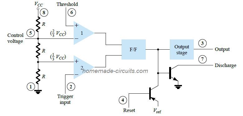 A standard IC555 consist of 25 transistors, 15 resistors and 2 diodes integrated on a silicon die.
There are two versions of the IC available namely military and civilian grade 555 timer.
The NE555 is a civilian grade IC and has operating temperature range of 0 to +70 degree Celsius.
The SE555 is military grade IC and has operating temperature range of -55 to +125 degree Celsius.
You will also find the CMOS version of timer known as 7555 and TLC555; these consume less power compared to standard 555 and operate less than 5V.
CMOS version timers consist of MOSFETs rather than bipolar transistor, which is efficient and consume less power.
A standard IC555 consist of 25 transistors, 15 resistors and 2 diodes integrated on a silicon die.
There are two versions of the IC available namely military and civilian grade 555 timer.
The NE555 is a civilian grade IC and has operating temperature range of 0 to +70 degree Celsius.
The SE555 is military grade IC and has operating temperature range of -55 to +125 degree Celsius.
You will also find the CMOS version of timer known as 7555 and TLC555; these consume less power compared to standard 555 and operate less than 5V.
CMOS version timers consist of MOSFETs rather than bipolar transistor, which is efficient and consume less power.
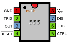 Pin 1: Ground or 0V: It's the negative supply pin of the IC
Pin 2: Trigger or input: A negative momentary trigger on this input pin causes the output pin3 to go HIGH.
This happens by a quick discharging of the timing capacitor below the lower threshold level of 1/3rd supply voltage.
The capacitor then slowly charges via the timing resistor, and when it rises above 2/3rd supply level, pin3 become LOW again.
This ON/OFF switching is done by an internal FLIP-FLOP stage.
Pin 3: Output: It's the output which responds to the input pins either by going high or low, or by oscillating ON/OFF
Pin 4: Reset: It's the reset pin which is always connected to the positive supply for normal working of the IC.
When grounded momentarily resets the IC output to its initial position, and if permanently connected to ground keeps the IC operations disabled.
Pin 5: Control: An external variable DC potential can be applied on this pin to control or modulate the pin3 pulse width, and generate a controlled PWM.
Pin 6: Threshold: This is the threshold pin which causes the output to go LOW (0V) as soon as the timing capacitor charge reaches the upper threshold of 2/3rd supply voltage.
Pin 7: Discharge: This is the discharge pin controlled by the internal flip flop, which forces the timing capacitor to discharge as soon as it has reached the 2/3rd supply voltage threshold level.
Pin 8: Vcc: It's the positive supply input between 5 V and 15 V.
Pin 1: Ground or 0V: It's the negative supply pin of the IC
Pin 2: Trigger or input: A negative momentary trigger on this input pin causes the output pin3 to go HIGH.
This happens by a quick discharging of the timing capacitor below the lower threshold level of 1/3rd supply voltage.
The capacitor then slowly charges via the timing resistor, and when it rises above 2/3rd supply level, pin3 become LOW again.
This ON/OFF switching is done by an internal FLIP-FLOP stage.
Pin 3: Output: It's the output which responds to the input pins either by going high or low, or by oscillating ON/OFF
Pin 4: Reset: It's the reset pin which is always connected to the positive supply for normal working of the IC.
When grounded momentarily resets the IC output to its initial position, and if permanently connected to ground keeps the IC operations disabled.
Pin 5: Control: An external variable DC potential can be applied on this pin to control or modulate the pin3 pulse width, and generate a controlled PWM.
Pin 6: Threshold: This is the threshold pin which causes the output to go LOW (0V) as soon as the timing capacitor charge reaches the upper threshold of 2/3rd supply voltage.
Pin 7: Discharge: This is the discharge pin controlled by the internal flip flop, which forces the timing capacitor to discharge as soon as it has reached the 2/3rd supply voltage threshold level.
Pin 8: Vcc: It's the positive supply input between 5 V and 15 V.
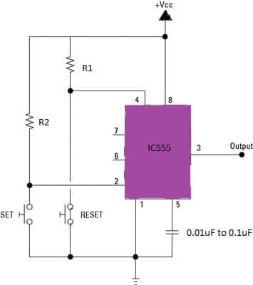 When the set button is depressed the output goes high and when reset button is depressed the output goes to low state.
R1 and R2 may be 10k ohm, the capacitor may be anywhere between the specified value.
When the set button is depressed the output goes high and when reset button is depressed the output goes to low state.
R1 and R2 may be 10k ohm, the capacitor may be anywhere between the specified value.
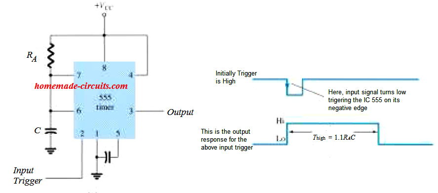
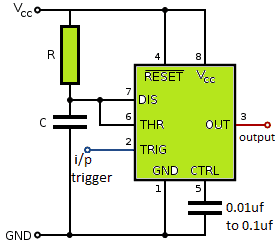
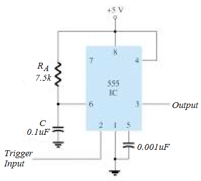 Solution:
Thigh = 1.1 RAC = 1.1(7.5 x 10³)(0.1 x 10⁻⁶) = 0.825 ms
Solution:
Thigh = 1.1 RAC = 1.1(7.5 x 10³)(0.1 x 10⁻⁶) = 0.825 ms
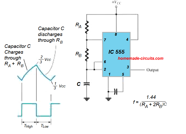 Along with this, the discharge transistor is switched ON, resulting in the pin 7 output discharging the capacitor via resistor RB.
This causes the voltage inside the capacitor to fall until finally it drops below the trigger level (VCC/3).
This action instantly triggers the flip flop stage of the IC, causing the output of the IC to go become high, turning OFF the discharge transistor.
This yet again enables the capacitor to get charged via resistors RA and RB toward VCC.
The time intervals
which is responsible for turning the output high and low can be calculated using
the relations
Thigh ¡Ö 0.7(RA + RB)C
Tlow ¡Ö 0.7 RBC
The total period is
T = period = Thigh + Tlow
Along with this, the discharge transistor is switched ON, resulting in the pin 7 output discharging the capacitor via resistor RB.
This causes the voltage inside the capacitor to fall until finally it drops below the trigger level (VCC/3).
This action instantly triggers the flip flop stage of the IC, causing the output of the IC to go become high, turning OFF the discharge transistor.
This yet again enables the capacitor to get charged via resistors RA and RB toward VCC.
The time intervals
which is responsible for turning the output high and low can be calculated using
the relations
Thigh ¡Ö 0.7(RA + RB)C
Tlow ¡Ö 0.7 RBC
The total period is
T = period = Thigh + Tlow
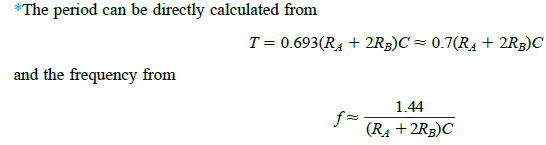
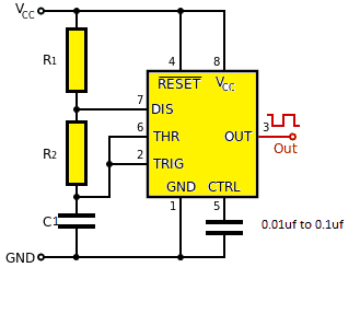 For 555 IC timers with bipolar transistors, R1 with low value must be avoided so that the output stays saturated near ground voltage during discharge process, else the ¡®low time¡¯ could be unreliable and we may see greater values for low time practically than calculated value.
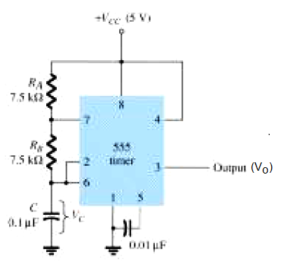 Solution:
 Waveform images can be seen below:
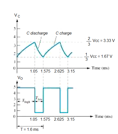
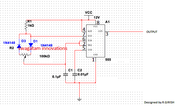 You can also design a 555 PWM circuit with variable duty cycle two diodes as shown in the above figure.
The PWM IC 555 circuit using two diodes is basically an astable circuit where the charge and discharge timing of the capacitor C1 is bifurcated through separate channels using diodes.
This modification enables the user to adjust the ON/OFF periods of the IC separately, and therefore achieve the desired PWM rate quickly.
You can also design a 555 PWM circuit with variable duty cycle two diodes as shown in the above figure.
The PWM IC 555 circuit using two diodes is basically an astable circuit where the charge and discharge timing of the capacitor C1 is bifurcated through separate channels using diodes.
This modification enables the user to adjust the ON/OFF periods of the IC separately, and therefore achieve the desired PWM rate quickly.
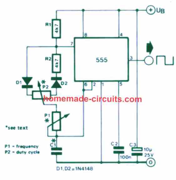 A tightly characterized charging time for capacitor C1 is established by the diodes D1 and D2.
This typically results in the duty cycle of around 50%, if it weren't for P2. For the present scenario the duty cycle is determined by the relationship between P1 and P2: n = 1 + P2/P1. For instance, if P2 = 0 (n = 100%), the frequency will then be:
f = 0.69 / [2(P1+P2+4.7k¦¸)C1
References: Stackexchange
A tightly characterized charging time for capacitor C1 is established by the diodes D1 and D2.
This typically results in the duty cycle of around 50%, if it weren't for P2. For the present scenario the duty cycle is determined by the relationship between P1 and P2: n = 1 + P2/P1. For instance, if P2 = 0 (n = 100%), the frequency will then be:
f = 0.69 / [2(P1+P2+4.7k¦¸)C1
References: Stackexchange
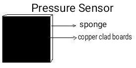

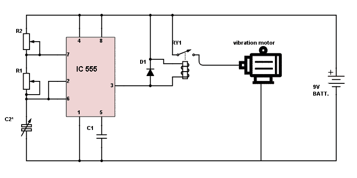
 This might help you out in getting out of the habit of walking in sleep.
But it is not an medical alternative.
Good luck!
This might help you out in getting out of the habit of walking in sleep.
But it is not an medical alternative.
Good luck!


 Moreover, a brushed motor can be operated by using an ordinary IC 555 PWM circuit, quite unlike a BLDC motor which requires much sophisticated control ICs which are not only difficult to find in the market, but are always vulnerable of becoming obsolete, risking the guarantee period of a E-rickshaw which might have incorporated that particular chip.
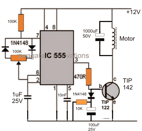 The 100k pot associated with the two 1N4148 diodes becomes responsible for varying the output PWMs at pin#3 of the IC, which in turn determines the conduction rate of the TIP142 transistor and the speed of the connected motor.
For higher current, the TIP142 could be replaced with equivalently rated mosfet.
The 100uF capacitor at the base of the transistor makes sure that whenever the E-rickshaw is initiated, it delivers a slow soft start to the motor, rather than with a jerk or at a higher initial torque.
The potentiometer should be of very high quality so that it is able to sustain the frequent speed control operations and may last for many many years without going through fatigue or mechanical wear and tear.
The 100k pot associated with the two 1N4148 diodes becomes responsible for varying the output PWMs at pin#3 of the IC, which in turn determines the conduction rate of the TIP142 transistor and the speed of the connected motor.
For higher current, the TIP142 could be replaced with equivalently rated mosfet.
The 100uF capacitor at the base of the transistor makes sure that whenever the E-rickshaw is initiated, it delivers a slow soft start to the motor, rather than with a jerk or at a higher initial torque.
The potentiometer should be of very high quality so that it is able to sustain the frequent speed control operations and may last for many many years without going through fatigue or mechanical wear and tear.
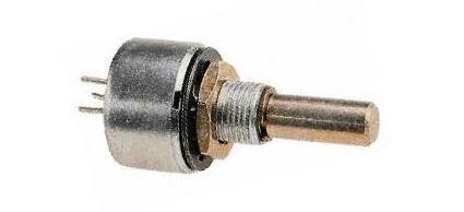 Typical specifications of the pot should be as given under:
Made up of Cermet or carbon moulded element.
Approved by BS and CECC
Rated at 2 watt at 70 degrees C, in Cermet
Rugged construction
Military standard layout
Container sealed with MC1/Mh2standards
Stiff, silver plated terminals.
Typical specifications of the pot should be as given under:
Made up of Cermet or carbon moulded element.
Approved by BS and CECC
Rated at 2 watt at 70 degrees C, in Cermet
Rugged construction
Military standard layout
Container sealed with MC1/Mh2standards
Stiff, silver plated terminals.

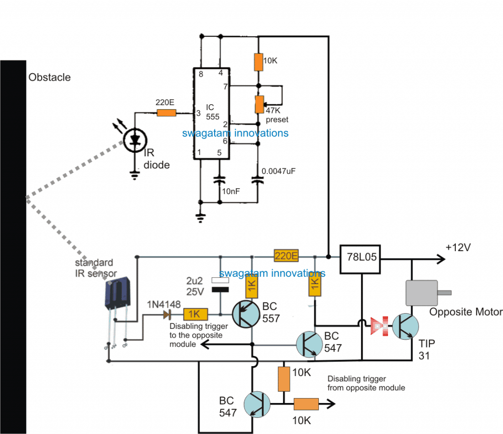 Now let's try to understand the above circuit with the help of the following explanation:
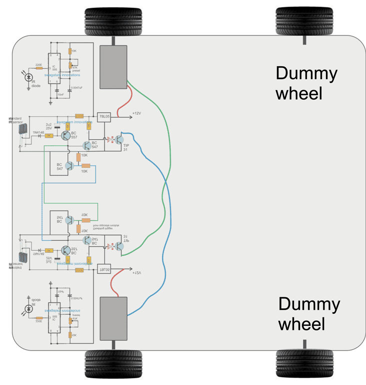 Update
A little thinking tells us that the above simple obstacle avoiding robot circuit could also be implemented by using a single module, instead of the two.
However a single module would allow the vehicle to carry out a single sided diversion every time it detects an obstacle, therefore the system could be configured either to take a clockwise diversion or anticlockwise diversion depending on which motor is connected with the circuit for the actions.
The example set up can be visualized in the following image:
Update
A little thinking tells us that the above simple obstacle avoiding robot circuit could also be implemented by using a single module, instead of the two.
However a single module would allow the vehicle to carry out a single sided diversion every time it detects an obstacle, therefore the system could be configured either to take a clockwise diversion or anticlockwise diversion depending on which motor is connected with the circuit for the actions.
The example set up can be visualized in the following image:
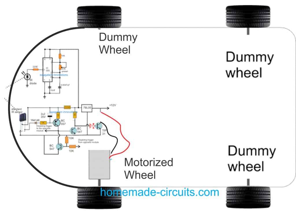 However, it seems there's one problem with the above single motor set up.
If suppose the vehicle encounters a right angled corner on the left side.
This will force the vehicle to keep moving anticlockwise, until it takes a U-turn, and begins moving back towards the same direction from where it had started.
This is not something the user would appreciate.
However, it seems there's one problem with the above single motor set up.
If suppose the vehicle encounters a right angled corner on the left side.
This will force the vehicle to keep moving anticlockwise, until it takes a U-turn, and begins moving back towards the same direction from where it had started.
This is not something the user would appreciate.
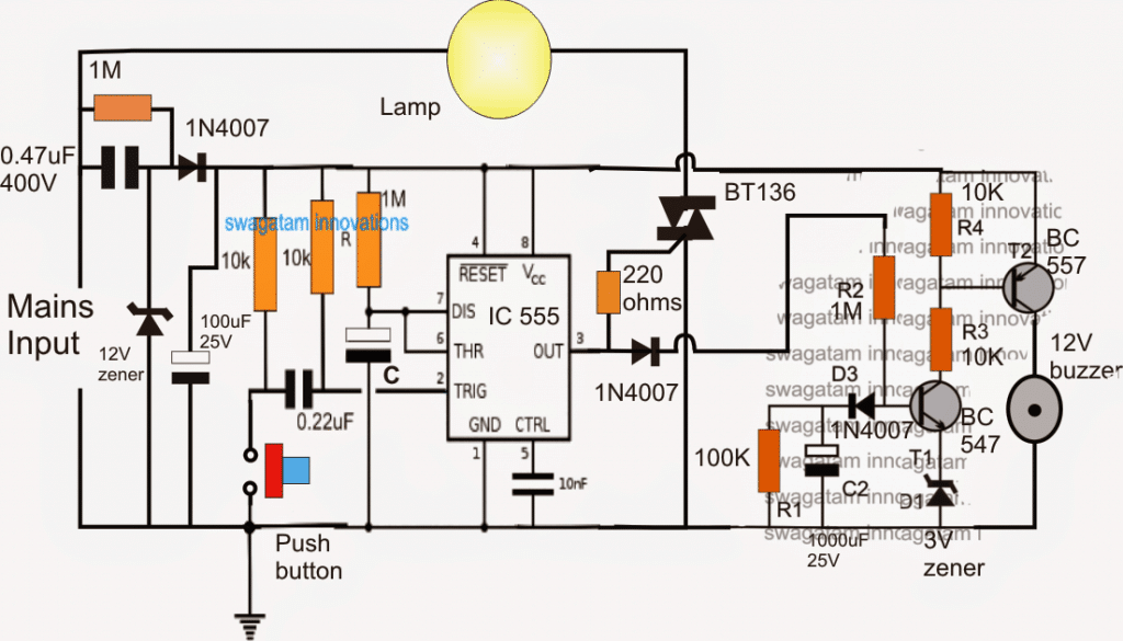
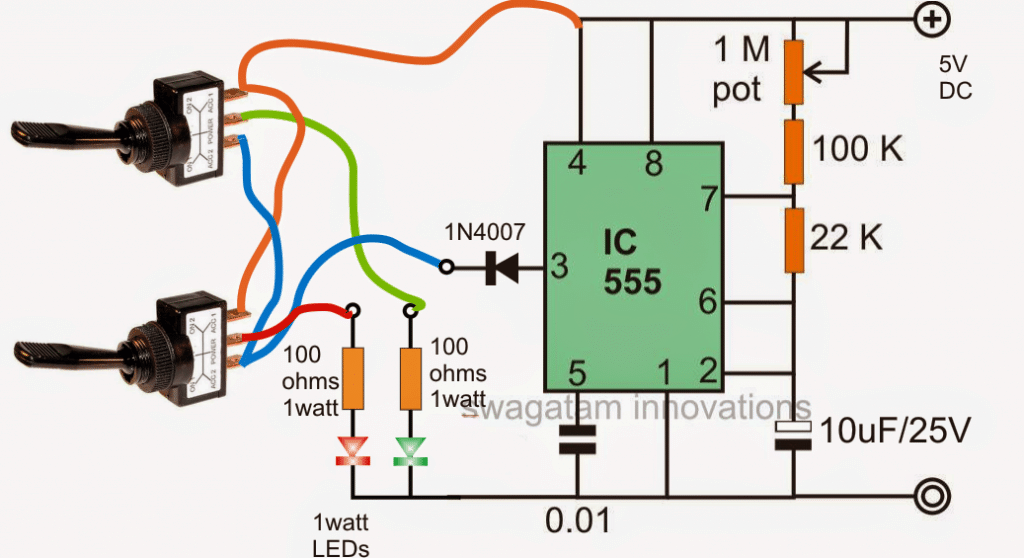 Referring to the above diagram, the circuit may be understood as explained below:

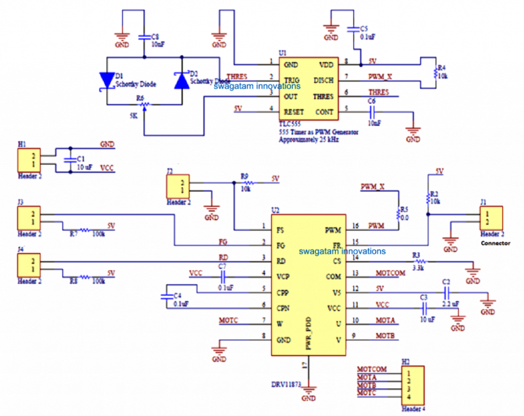
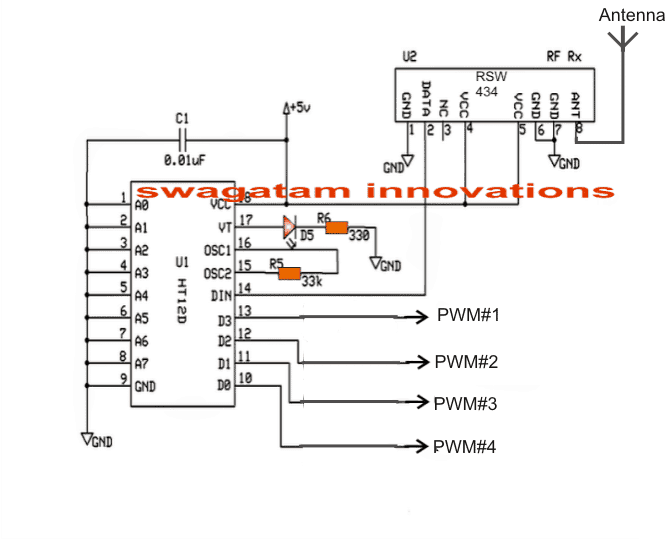 The above circuit shows the receiver remote RF circuit which is supposed to be accommodated inside the quadcopter for receiving an external wireless PWM data from the user¡¯s remote transmitter handset and then process the signals appropriately in order to feed the accompanying DRV controller modules as explained in the previous section.
The 4 outputs named as PWM#1¡.PWM#4 needs to be connected with the PWM pin#15 of the DRV IC as indicated in the previous diagram.
These PWM pinouts from the RF receiver unit becomes activated whenever the corresponding button is pressed by the user in its transmitter handset.
The above circuit shows the receiver remote RF circuit which is supposed to be accommodated inside the quadcopter for receiving an external wireless PWM data from the user¡¯s remote transmitter handset and then process the signals appropriately in order to feed the accompanying DRV controller modules as explained in the previous section.
The 4 outputs named as PWM#1¡.PWM#4 needs to be connected with the PWM pin#15 of the DRV IC as indicated in the previous diagram.
These PWM pinouts from the RF receiver unit becomes activated whenever the corresponding button is pressed by the user in its transmitter handset.
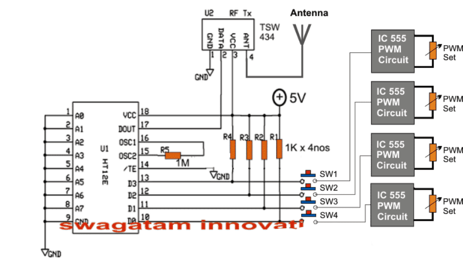 The circuit shown above exhibits the wiring details of the transmitter module.
The idea looks pretty simple, the main transmitter circuit is formed by the TSW434 chip which transmits the encoded PWM signals into the atmosphere, and the HT12E which becomes responsible for feeding the encoded signals to the TSW chip.
The PWM signals are generated by 4 separate IC 555 circuit stages which may be identical to the one which was earlier discussed in the DRV controller module.
The PWM contents of the 4 ICs can be seen terminated to the respective pinouts of the encoder IC HT12E through 4 discrete push buttons indicated as SW1----SW4.
Each of these buttons correspond and toggle the identical pinout of the receiver module which we discussed earlier and indicated as PWM#1, PWM#2¡..PWM#4.
Meaning pressing SW1 may cause the PWM#1 output of the receiver unit active and this will pinout will start feeding the received decoded PWM signals from the transmitter to the associated DRV module and in turn cause the relevant motor to change its speed accordingly.
Similarly, pressing SW2,3,4 can be used for influencing the speeds of the other 3 quadcopter motors as per the users wish.
The circuit shown above exhibits the wiring details of the transmitter module.
The idea looks pretty simple, the main transmitter circuit is formed by the TSW434 chip which transmits the encoded PWM signals into the atmosphere, and the HT12E which becomes responsible for feeding the encoded signals to the TSW chip.
The PWM signals are generated by 4 separate IC 555 circuit stages which may be identical to the one which was earlier discussed in the DRV controller module.
The PWM contents of the 4 ICs can be seen terminated to the respective pinouts of the encoder IC HT12E through 4 discrete push buttons indicated as SW1----SW4.
Each of these buttons correspond and toggle the identical pinout of the receiver module which we discussed earlier and indicated as PWM#1, PWM#2¡..PWM#4.
Meaning pressing SW1 may cause the PWM#1 output of the receiver unit active and this will pinout will start feeding the received decoded PWM signals from the transmitter to the associated DRV module and in turn cause the relevant motor to change its speed accordingly.
Similarly, pressing SW2,3,4 can be used for influencing the speeds of the other 3 quadcopter motors as per the users wish.
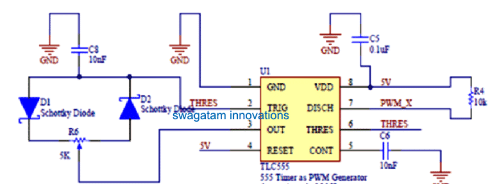 Please remember that the 5K pot could be in the form of a usual pot and this pot could be used additionally with the buttons for selecting different speeds on the corresponding motors.
Meaning by keeping a selected button pressed and simultaneously moving the corresponding 5KPWMpot one can cause the quadcopter to increase or decrease its speed in the intended direction.
Alternatively the PWM could be initially set at some higher or lower level and then the corresponding button pressed to enable the corresponding quadcopter motor to attain the preferred speed, as per the PWM setting.
Please remember that the 5K pot could be in the form of a usual pot and this pot could be used additionally with the buttons for selecting different speeds on the corresponding motors.
Meaning by keeping a selected button pressed and simultaneously moving the corresponding 5KPWMpot one can cause the quadcopter to increase or decrease its speed in the intended direction.
Alternatively the PWM could be initially set at some higher or lower level and then the corresponding button pressed to enable the corresponding quadcopter motor to attain the preferred speed, as per the PWM setting.
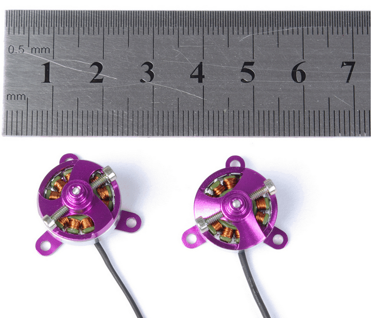
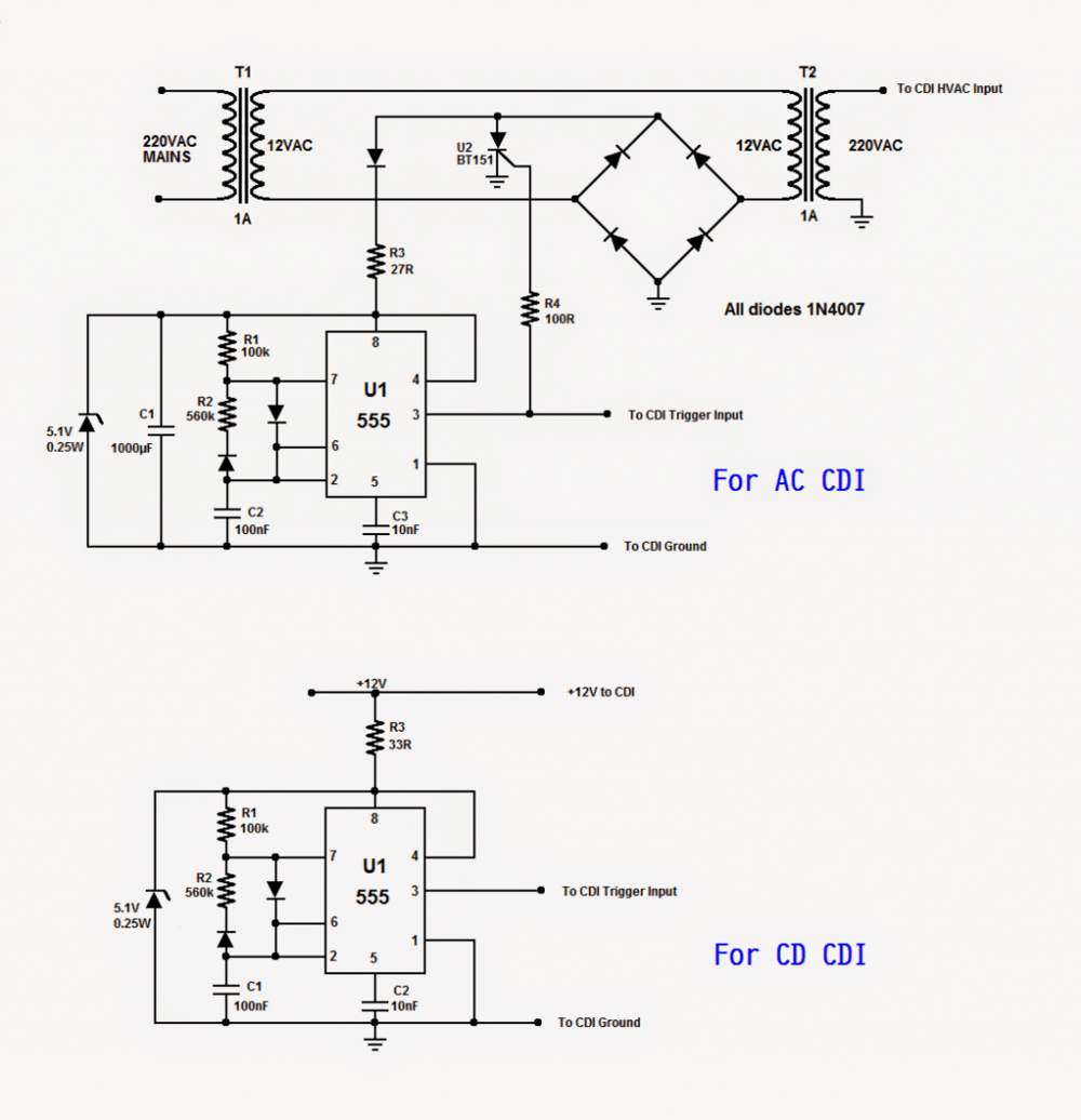
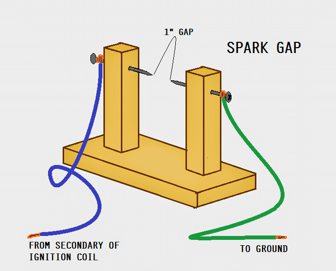
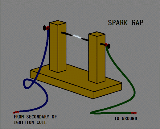

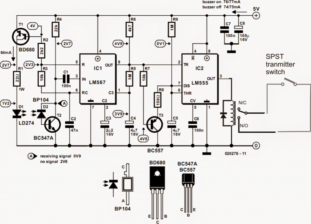


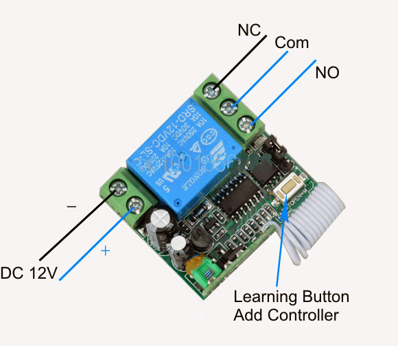 The relay contacts of the Rx unit as indicated in the above image may be appropriately wired with an audible alarm system or any other desired form of recordable alarm system.
In the above discussion we understood the details regarding the building and installing of the proposed remote controlled home security circuit system, now it's time to identify how the Tx may be powered through a solar rechargeable battery circuit.
The relay contacts of the Rx unit as indicated in the above image may be appropriately wired with an audible alarm system or any other desired form of recordable alarm system.
In the above discussion we understood the details regarding the building and installing of the proposed remote controlled home security circuit system, now it's time to identify how the Tx may be powered through a solar rechargeable battery circuit.

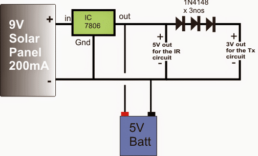 The above 5V solar battery charger circuit may be used for powering the remote detector transmitter assembly, the whole system along with the panel and the circuits may be positioned over a tree or some kind reinforced steel structure on the ground, and camouflaged appropriately.
This concludes the article regarding a cheap yet effective home security circuit which enables the user to detect an intrusion in advance, which may take place far away across the lanes or passages finally leading to the user's house.
The article details only one such module, although many such self contained remote IR modules may be built and installed across zig-zag lanes, enabling multiple tracking and detection for the target.
Feedback from Mr.
Dave
Wow Swag, I am so impressed.
I have a few simple questions:
1. What type of range could be expected with the simple push button style tx and rx
module pair shown in the picture? (Maybe 100m max??)
2. What would/could you use if the requirement was say 1000m? (I see guys flying FPV
drones or planes over 5000m online)
3. How expensive might a tx/rx module pair capable of 1000m be? Can you suggest a
model or location to buy?
4. Several spots on your schematic you have labels like "4V9", I thinking this must
mean 4.9V when using a 5.0V battery.
Am I reading the schematic right??
Thanks so much.
Now I need to order the parts and get building.
Thank you Dave =)
Here are the answers:
1) Yes the range is around 100 meters for the specified Tx, Rx modules
2) There are a few long range options available online, there's one that uses the IC PT2262 and is assigned to provide a good 2km range, the datasheet of the device may be studied in the following link:
https://pdf.datasheetcatalog.com/datasheet/PrincetonTechnologyCorporation/mXusxsq.pdf
However the relay stage is not included in the module which you may have
to associate for the required actions.
It can be simply done by
integrating a relay driver stage with the "OUT" pin of the Rx module.
3) The indicated cost appears to be around $18.....
4) yes you are reading the schematic absolutely correctly:)
By the way if you prefer to use a PIR circuit, you may switch to the
following design.
https://www.homemade-circuits.com/2014/09/automatic-pir-controlled-fan-circuit.html
Best Regards
Swag
In case a PIR is preferred instead of the discussed IC 567 tuned IR design, the same may be achieved by integrating the PIR system with the RF modules as shown in the following diagram:
The above 5V solar battery charger circuit may be used for powering the remote detector transmitter assembly, the whole system along with the panel and the circuits may be positioned over a tree or some kind reinforced steel structure on the ground, and camouflaged appropriately.
This concludes the article regarding a cheap yet effective home security circuit which enables the user to detect an intrusion in advance, which may take place far away across the lanes or passages finally leading to the user's house.
The article details only one such module, although many such self contained remote IR modules may be built and installed across zig-zag lanes, enabling multiple tracking and detection for the target.
Feedback from Mr.
Dave
Wow Swag, I am so impressed.
I have a few simple questions:
1. What type of range could be expected with the simple push button style tx and rx
module pair shown in the picture? (Maybe 100m max??)
2. What would/could you use if the requirement was say 1000m? (I see guys flying FPV
drones or planes over 5000m online)
3. How expensive might a tx/rx module pair capable of 1000m be? Can you suggest a
model or location to buy?
4. Several spots on your schematic you have labels like "4V9", I thinking this must
mean 4.9V when using a 5.0V battery.
Am I reading the schematic right??
Thanks so much.
Now I need to order the parts and get building.
Thank you Dave =)
Here are the answers:
1) Yes the range is around 100 meters for the specified Tx, Rx modules
2) There are a few long range options available online, there's one that uses the IC PT2262 and is assigned to provide a good 2km range, the datasheet of the device may be studied in the following link:
https://pdf.datasheetcatalog.com/datasheet/PrincetonTechnologyCorporation/mXusxsq.pdf
However the relay stage is not included in the module which you may have
to associate for the required actions.
It can be simply done by
integrating a relay driver stage with the "OUT" pin of the Rx module.
3) The indicated cost appears to be around $18.....
4) yes you are reading the schematic absolutely correctly:)
By the way if you prefer to use a PIR circuit, you may switch to the
following design.
https://www.homemade-circuits.com/2014/09/automatic-pir-controlled-fan-circuit.html
Best Regards
Swag
In case a PIR is preferred instead of the discussed IC 567 tuned IR design, the same may be achieved by integrating the PIR system with the RF modules as shown in the following diagram:
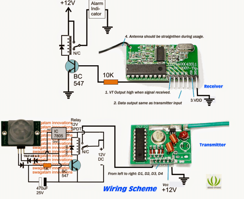 The above wireless home security circuit is self explanatory, the relevant components simply needs to be wired as per the given instructions in the above diagram.
If you have doubts or confusions please feel free to comment below:
The above wireless home security circuit is self explanatory, the relevant components simply needs to be wired as per the given instructions in the above diagram.
If you have doubts or confusions please feel free to comment below:
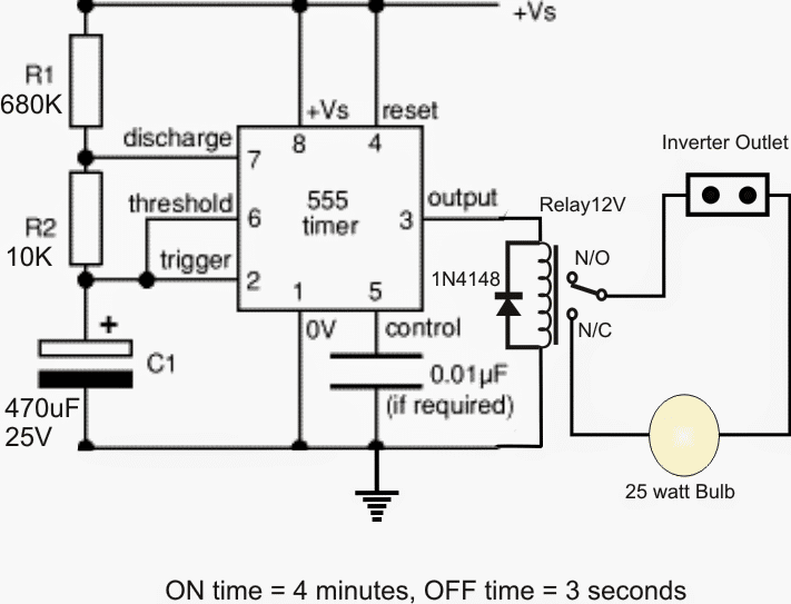 Feedback
Hi Swagatam,
Thanks for the guidance, it worked..
I followed the second half of your suggestion about using a 25 watt load and it served my purpose to a significant extent.I connected a 25 Watt Bulb to the UPS, now it gives a run time of almost one hour and 10 minutes,
Have been using cum testing it for the past 10 days..and feel highly pleased..despite it being little inefficient.
Now coming back to the 555 timer, I found the IC on ebay, How do I program the timer for 2 second ON and 4.8 Minutes off ??
Any special equipment needed ?
Feedback
Hi Swagatam,
Thanks for the guidance, it worked..
I followed the second half of your suggestion about using a 25 watt load and it served my purpose to a significant extent.I connected a 25 Watt Bulb to the UPS, now it gives a run time of almost one hour and 10 minutes,
Have been using cum testing it for the past 10 days..and feel highly pleased..despite it being little inefficient.
Now coming back to the 555 timer, I found the IC on ebay, How do I program the timer for 2 second ON and 4.8 Minutes off ??
Any special equipment needed ?
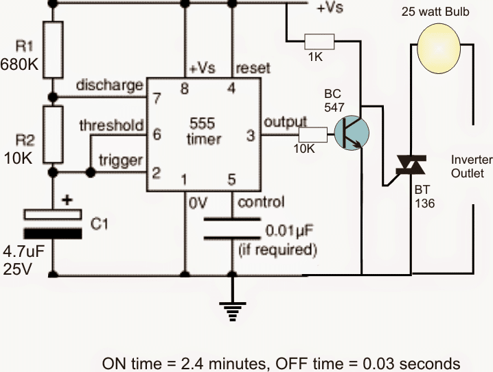 The above circuit will rapidly switch ON and OFF the load (25 watt bulb) at the indicated rate (2.4 seconds OFF, 0.03 seconds ON) keeping the load just dimly lit, and also tricking the inverter to "think" that the inverter is loaded, preventing the auto shut down.

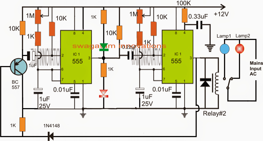
 The shown set up indicates a solar panel placed at the top of the structure, the high voltage collector mesh can be seen clamped vertically just below the solar panel, while a LED can be witnessed positioned beside the mesh trap.
The battery and the circuit are enclosed inside a wooden "house" like structure which becomes the base for all the above described fabrications.
The slanting roof of the house shaped cabinet ensures that the insects slide and fall down on the ground while they hit the mesh and get killed.
The bulb is used for attracting the insects, as we all know that any form of light attracts insects towards it and the same principle works here for luring the insects near the high voltage mesh trap.
The bulb could be either an LED lamp, a low wattage CFL lamp or even a black light or an UV wood's lamp.
The shown set up indicates a solar panel placed at the top of the structure, the high voltage collector mesh can be seen clamped vertically just below the solar panel, while a LED can be witnessed positioned beside the mesh trap.
The battery and the circuit are enclosed inside a wooden "house" like structure which becomes the base for all the above described fabrications.
The slanting roof of the house shaped cabinet ensures that the insects slide and fall down on the ground while they hit the mesh and get killed.
The bulb is used for attracting the insects, as we all know that any form of light attracts insects towards it and the same principle works here for luring the insects near the high voltage mesh trap.
The bulb could be either an LED lamp, a low wattage CFL lamp or even a black light or an UV wood's lamp.
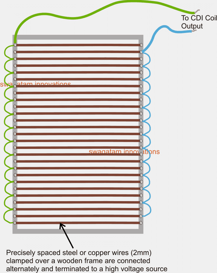
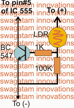
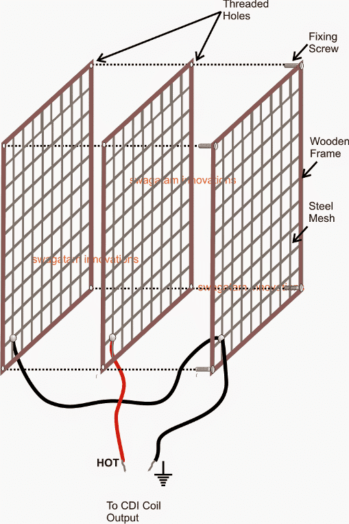 Referring to the shown diagram the mesh assembly is built by fitting three identical sets of readymade fine iron or steel nets with a help of a few well fabricated square wooden frames.
After securing the steel nets within the wooden frames, these are tightly screwed together face to face using nuts and bolts and spacers such that the three frames acquire an optimized distance from each other.
The above assembly actually becomes the most tedious and the crucial part of the system and once this is completed, making the high voltage mosquito killer circuit can be rather simply done with the help of the following circuit.
Referring to the shown diagram the mesh assembly is built by fitting three identical sets of readymade fine iron or steel nets with a help of a few well fabricated square wooden frames.
After securing the steel nets within the wooden frames, these are tightly screwed together face to face using nuts and bolts and spacers such that the three frames acquire an optimized distance from each other.
The above assembly actually becomes the most tedious and the crucial part of the system and once this is completed, making the high voltage mosquito killer circuit can be rather simply done with the help of the following circuit.

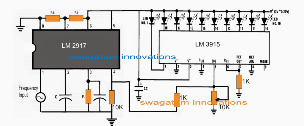 Referring to the above circuit schematic, we can see two IC stages, the left IC LM2917 forms a precise frequency to voltage converter, while the IC LM3915 is rigged as a LED dot mode voltage indicator stage.
The entire circuit is supposed to convert a varying frequency into a correspondingly shifting LED across the shown 10 LED outputs of the IC LM3915.
So basically any fluctuating frequency fed across pin#1 of IC LM2917 is appropriately converted into rising or declining voltage levels at its pin#4, which is fed at the sensing input pin#5 of the LM3915. This signal is instantly converted into an advancing LED "dot" across the given LED array from pin#1 to pin#10 of the IC LM3915.
The illuminated position of any of the LED across the given 10 outputs indicates the frequency level that may be available at pin#1 of the left IC.
The idea here is to set different frequency levels for the 12 valves through a IC 555 such that toggling of the particular valve produces a unique frequency, which may be further fed to the input of the above explained circuit.
Depending upon the frequency level, the corresponding LED may be expected to light up, thereby indicating which valve was activated at the remote location.
As we can see, a variety of signals (10 or 12) can be transmitted from the valve mechanism to the remote LED indicator location using just two wires, as requested in the above section of the article.
Referring to the above circuit schematic, we can see two IC stages, the left IC LM2917 forms a precise frequency to voltage converter, while the IC LM3915 is rigged as a LED dot mode voltage indicator stage.
The entire circuit is supposed to convert a varying frequency into a correspondingly shifting LED across the shown 10 LED outputs of the IC LM3915.
So basically any fluctuating frequency fed across pin#1 of IC LM2917 is appropriately converted into rising or declining voltage levels at its pin#4, which is fed at the sensing input pin#5 of the LM3915. This signal is instantly converted into an advancing LED "dot" across the given LED array from pin#1 to pin#10 of the IC LM3915.
The illuminated position of any of the LED across the given 10 outputs indicates the frequency level that may be available at pin#1 of the left IC.
The idea here is to set different frequency levels for the 12 valves through a IC 555 such that toggling of the particular valve produces a unique frequency, which may be further fed to the input of the above explained circuit.
Depending upon the frequency level, the corresponding LED may be expected to light up, thereby indicating which valve was activated at the remote location.
As we can see, a variety of signals (10 or 12) can be transmitted from the valve mechanism to the remote LED indicator location using just two wires, as requested in the above section of the article.
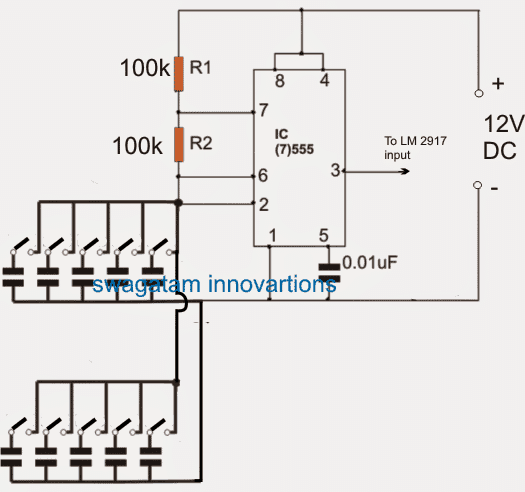 In the above diagram we are able to see, an IC 555 wired as an astable multivibrator circuit, wherein 10 individual capacitors with incrementing values are configured across the pin6/2 and ground of the IC.
These capacitors are toggled by the 10 discrete relay contacts which in turn force the IC to generate the corresponding frequency at the calculated level, at its pin#3.
The relay coils attached with these contacts are rigged with the valve outputs such that the relevant relay coil gets energized as as soon as the matching valve is activated.
The above action causes the IC to generate a corresponding level of frequency which is transmitted through a pair of wires to the indicator circuit's input.
As explained in the initial section of the article, the IC LM2917 reacts to this input, converting it into a corresponding magnitude of voltage level for the IC LM3915.
LM3915 accepts the voltage level and illuminates the particular LED in response to the fed frequency level from the IC 555 circuit.
In the above diagram we are able to see, an IC 555 wired as an astable multivibrator circuit, wherein 10 individual capacitors with incrementing values are configured across the pin6/2 and ground of the IC.
These capacitors are toggled by the 10 discrete relay contacts which in turn force the IC to generate the corresponding frequency at the calculated level, at its pin#3.
The relay coils attached with these contacts are rigged with the valve outputs such that the relevant relay coil gets energized as as soon as the matching valve is activated.
The above action causes the IC to generate a corresponding level of frequency which is transmitted through a pair of wires to the indicator circuit's input.
As explained in the initial section of the article, the IC LM2917 reacts to this input, converting it into a corresponding magnitude of voltage level for the IC LM3915.
LM3915 accepts the voltage level and illuminates the particular LED in response to the fed frequency level from the IC 555 circuit.
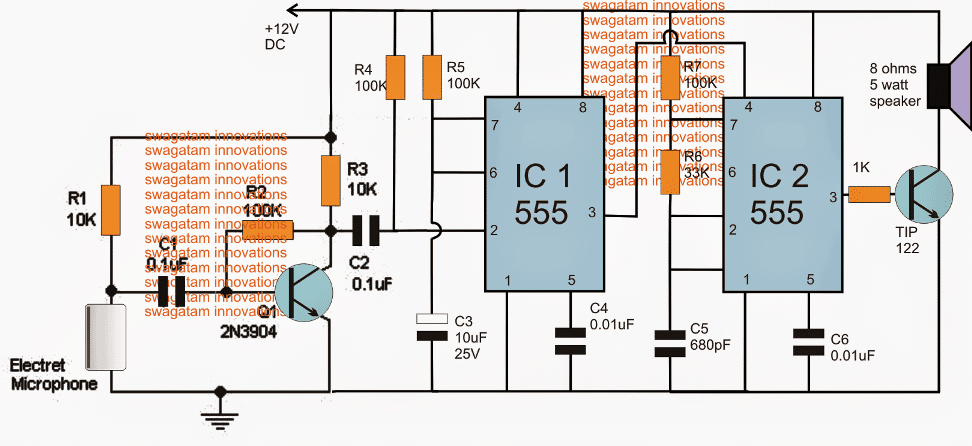 Note: Please use 1uF capacitor for C2 to ensure a foolproof triggering of the IC1 stage...
Parts List
Resistors all 1/4 watt 5%
R1, R3 = 10K
R2, R4, R5, R7 = 100K
R6 = 33K
R7 = 1K
Capacitors
C1 = 0.1uF, disc ceramic
C2 = 1uF/25V
C3 = 10uF/25v
C4, C6 = 0.01uF ceramic
C5 = 680pF ceramic
Transistors
Q1 = 2N3904 or BC547
Q2 = TIP122
Referring to the above shown dog bark inhibitor circuit, we can see three distinct stages involved, the sound sensor and preamplifier circuit using the Q1 and the electret MIC stage, the monostable stage using IC1 and the associated parts and the ultrasonic sound generator stage using the IC2 and the speaker driver stage.
Whenever a dog barks, the Mic detects it causing a sequential low and high pulse at the base of T1. T1 responds to this and produces an equivalent amplified signal across C2, which in turn triggers the pin#2 of the monostable IC1.
The above action forces IC1 to produce a high at its pin#3 for a period determined by the values of R5/C3.
This high at pin#3 of IC1 enables the reset pin#4 of IC2 to become active thereby allowing the astable IC2 to supply the ultrasonic pulse at its pin#3, which is appropriately amplified by the associated TIP122 transistor, driving the connected speaker.
The speaker vibrates at the specified amplified level throwing the ultrasonic sound in the direction where the dogs need to be driven away.
The above sound waves is supposed to fluster the dogs and cause a lot of disturbance in their ears due to its high pitched sound, and also due to its synchronized effect with the dog's own barking sequence.
Actually the above dog barking stopping device might respond to all types of high dB sound levels, however since it won't be audible to a human ear this will never be an issue, and may be ignored.
Note: Please use 1uF capacitor for C2 to ensure a foolproof triggering of the IC1 stage...
Parts List
Resistors all 1/4 watt 5%
R1, R3 = 10K
R2, R4, R5, R7 = 100K
R6 = 33K
R7 = 1K
Capacitors
C1 = 0.1uF, disc ceramic
C2 = 1uF/25V
C3 = 10uF/25v
C4, C6 = 0.01uF ceramic
C5 = 680pF ceramic
Transistors
Q1 = 2N3904 or BC547
Q2 = TIP122
Referring to the above shown dog bark inhibitor circuit, we can see three distinct stages involved, the sound sensor and preamplifier circuit using the Q1 and the electret MIC stage, the monostable stage using IC1 and the associated parts and the ultrasonic sound generator stage using the IC2 and the speaker driver stage.
Whenever a dog barks, the Mic detects it causing a sequential low and high pulse at the base of T1. T1 responds to this and produces an equivalent amplified signal across C2, which in turn triggers the pin#2 of the monostable IC1.
The above action forces IC1 to produce a high at its pin#3 for a period determined by the values of R5/C3.
This high at pin#3 of IC1 enables the reset pin#4 of IC2 to become active thereby allowing the astable IC2 to supply the ultrasonic pulse at its pin#3, which is appropriately amplified by the associated TIP122 transistor, driving the connected speaker.
The speaker vibrates at the specified amplified level throwing the ultrasonic sound in the direction where the dogs need to be driven away.
The above sound waves is supposed to fluster the dogs and cause a lot of disturbance in their ears due to its high pitched sound, and also due to its synchronized effect with the dog's own barking sequence.
Actually the above dog barking stopping device might respond to all types of high dB sound levels, however since it won't be audible to a human ear this will never be an issue, and may be ignored.
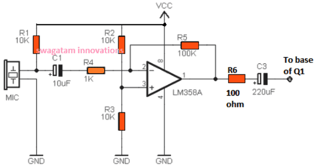 Once you build the above circuit, you can eliminate or remove R1, R2, C1 from the first circuit, and replace it with the mentioned op amp based MIC amplifier circuit and configure the C3 output from the op amp with the base of Q1.
This upgrade will ensure that the circuit responds appropriately even to weak sound signals, specifically dog barking sound during night time, and trigger the IC 555 stages for the intended results.
Once you build the above circuit, you can eliminate or remove R1, R2, C1 from the first circuit, and replace it with the mentioned op amp based MIC amplifier circuit and configure the C3 output from the op amp with the base of Q1.
This upgrade will ensure that the circuit responds appropriately even to weak sound signals, specifically dog barking sound during night time, and trigger the IC 555 stages for the intended results.
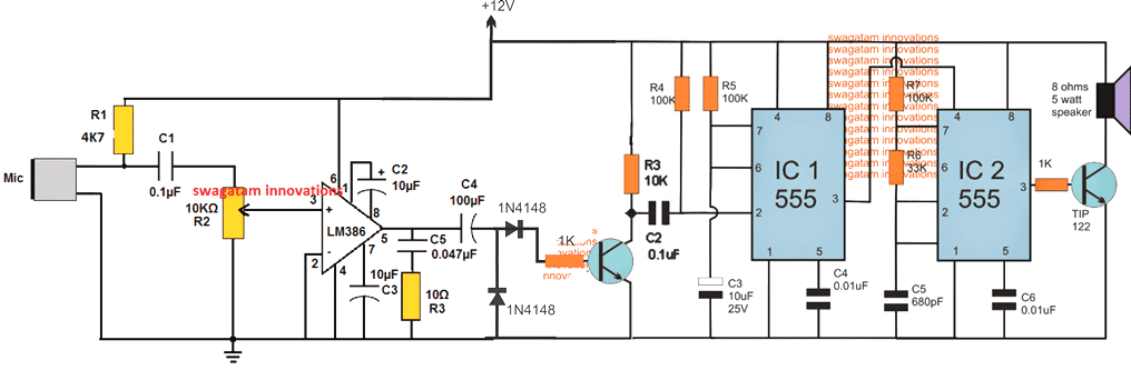
 The parts list for the above design is shown below:
R1 = 5k6
R2 = 47k
R3 = 3M3
R4 = 33K
R5 = 330 OHMS
R6 = 2K2
C1 = 0.1uF
C2 = 1uF/25V
T1, T2 = BC547
T3 = TIP127
D1 = 1N4007
Mic = electret condenser MIC.
If you wish to use some other form of deterrent instead of the indicated high power alarm, you can replace the speaker with a relay and connect the desired load with the relay contacts.
The relay based design is demonstrated in the following diagram:
The parts list for the above design is shown below:
R1 = 5k6
R2 = 47k
R3 = 3M3
R4 = 33K
R5 = 330 OHMS
R6 = 2K2
C1 = 0.1uF
C2 = 1uF/25V
T1, T2 = BC547
T3 = TIP127
D1 = 1N4007
Mic = electret condenser MIC.
If you wish to use some other form of deterrent instead of the indicated high power alarm, you can replace the speaker with a relay and connect the desired load with the relay contacts.
The relay based design is demonstrated in the following diagram:
 The parts list will be the same as above, except the T3, which can be replaced with BC557 transistor.
 Note: Please use a Darlington BC547 configuration at pin#5 of IC2 instead of a single BC547. This will produce a more effective responsecompared to a single BC547
 ##PLEASE CONNECT A 1K FROM PIN5 OF IC2 TO GROUND, WHICH IS MISTAKENLY NOT SHOWN IN THE ABOVE DESIGN##
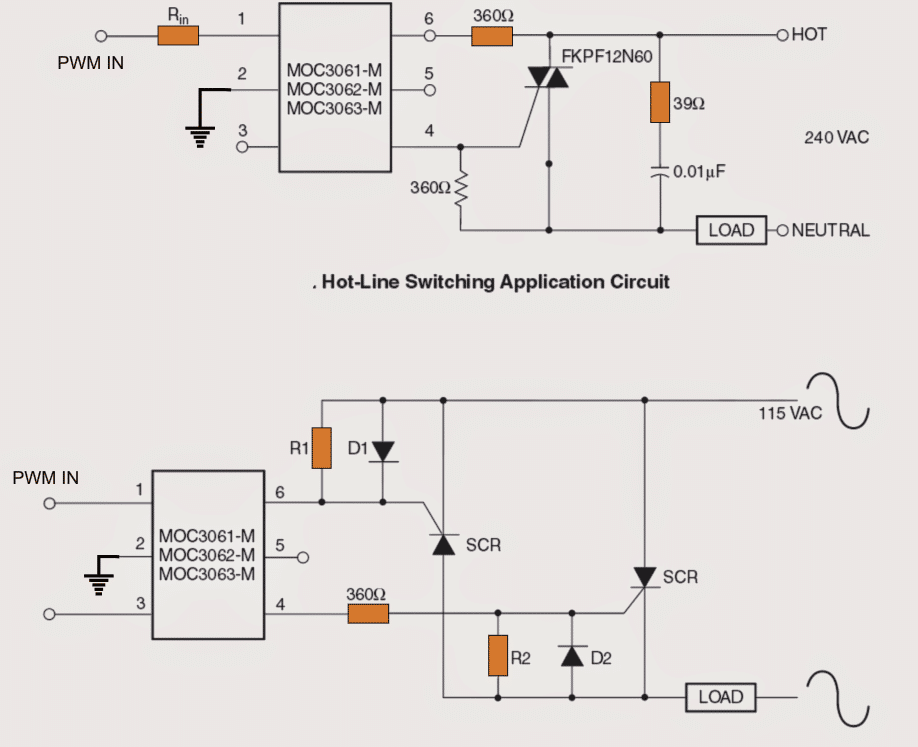 The above image shows how the switch ON soft start PWM control may be implemented on heavy motors for the intended purpose.
In the image above we see how triac driver isolators with zero crossing detector can be employed for driving the motors with the linearly incrementing PWMs for executing a soft start effect.
The above concept effectively takes care of the start ON overcurrent situating on single phase motors.
However in case a 3 phase motor is used, the following idea can be used for implementing the proposed 3 phase soft start on motors.
The above image shows how the switch ON soft start PWM control may be implemented on heavy motors for the intended purpose.
In the image above we see how triac driver isolators with zero crossing detector can be employed for driving the motors with the linearly incrementing PWMs for executing a soft start effect.
The above concept effectively takes care of the start ON overcurrent situating on single phase motors.
However in case a 3 phase motor is used, the following idea can be used for implementing the proposed 3 phase soft start on motors.
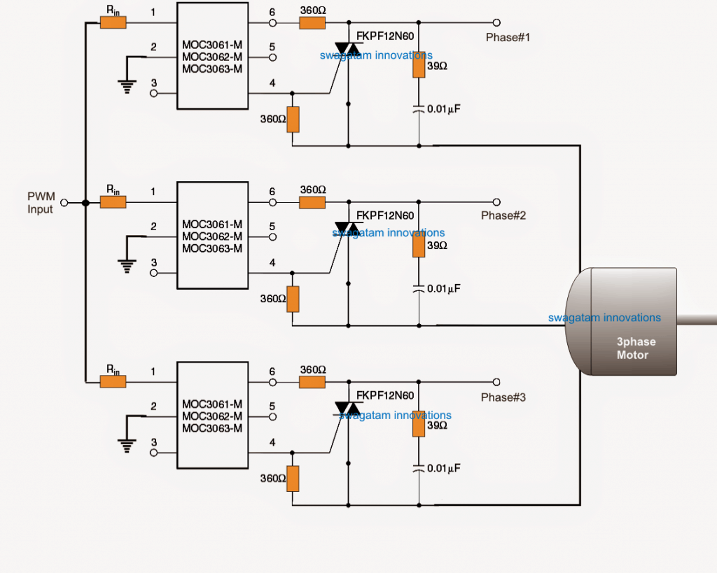
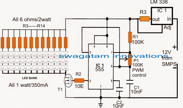 In the image above, the supply is acquired from an SMPS unit which applied to the PWM circuit through a LM338 current controller circuit stage.
The pot P1 is used for adjusting the PWM duty cycles to the LED bank for achieving the desired intensity levels.
The resistor R3 determines the limiting current level from the IC LM338, it may be calculated with the following formula:
R3 = 1.25/LED current
The circuit shows a 36 LED (1 watt each) bank being driven by the PWM and the current controller stages.
The LED series resistors are introduced for safeguarding each 3 LED string from over voltage.
since the total forward voltage drop of the strings constitute to 3.3 x 3 = 9.9V and the supply voltage 12V that's about 2V higher.
R3 controls the overall current for the entire LED bank, and may be calculated by using the above mentioned formula, for the shown design the result may be calculated as:
R3 = 1.25/0.35 x 12 = 0.29 Ohms
Wattage = 1.25 x 0.35 x 12 = 5.25 watts, here 0.35 is the current through each LED string, 12 is the number of strings, and 1.25 is the fixed reference as specified by the IC LM338 datasheet.
With a little effort you can skip the LM338 stage by modifying your existing SMPS unit to any desired maximum current limit, as per the specs of the LED, the entire procedure may be learned below:
How to make a variable current SMPS circuit
In the image above, the supply is acquired from an SMPS unit which applied to the PWM circuit through a LM338 current controller circuit stage.
The pot P1 is used for adjusting the PWM duty cycles to the LED bank for achieving the desired intensity levels.
The resistor R3 determines the limiting current level from the IC LM338, it may be calculated with the following formula:
R3 = 1.25/LED current
The circuit shows a 36 LED (1 watt each) bank being driven by the PWM and the current controller stages.
The LED series resistors are introduced for safeguarding each 3 LED string from over voltage.
since the total forward voltage drop of the strings constitute to 3.3 x 3 = 9.9V and the supply voltage 12V that's about 2V higher.
R3 controls the overall current for the entire LED bank, and may be calculated by using the above mentioned formula, for the shown design the result may be calculated as:
R3 = 1.25/0.35 x 12 = 0.29 Ohms
Wattage = 1.25 x 0.35 x 12 = 5.25 watts, here 0.35 is the current through each LED string, 12 is the number of strings, and 1.25 is the fixed reference as specified by the IC LM338 datasheet.
With a little effort you can skip the LM338 stage by modifying your existing SMPS unit to any desired maximum current limit, as per the specs of the LED, the entire procedure may be learned below:
How to make a variable current SMPS circuit
 As we can see, the above configuration is identical to the first one, barring the addition of the voltage booster stage between pin3 of the IC 555 and the mosfet gate.
Here a couple of diodes and capacitors effectively raise the pin3 PWM level from 5V peak to 10V peak, this becomes imperative since a mosfet is being used for the regulations, and mosfets do not respond optimally with gate voltages lower than 9V.
The shown mosfet gate voltage booster stage can be also applied with PWM outputs that may be derived from an Arduino board or other MCUs.
As we can see, the above configuration is identical to the first one, barring the addition of the voltage booster stage between pin3 of the IC 555 and the mosfet gate.
Here a couple of diodes and capacitors effectively raise the pin3 PWM level from 5V peak to 10V peak, this becomes imperative since a mosfet is being used for the regulations, and mosfets do not respond optimally with gate voltages lower than 9V.
The shown mosfet gate voltage booster stage can be also applied with PWM outputs that may be derived from an Arduino board or other MCUs.
 Th figure above shows a basic atomizer PWM heat controller circuit using just a couple of transistors and a single mosfet.
The mosfet could be replaced with a BJT if the operating voltage is below 6V.
The circuit is a basic transistorized astable multivibrator circuit, the variable resistor VR1 decides the PWM rate for the two arms of the astable.
The LED provides an opposite indication for the PWM rates applied at the gate of the mofet.
Brighter illumination indicates a narrower PWMs on the mosfet gate and therefore lower heat on the coil, conversely a dimming LED indicates a wider PWMs on the mosfet gate and consequently greater heat on the connected filament coil.
Th figure above shows a basic atomizer PWM heat controller circuit using just a couple of transistors and a single mosfet.
The mosfet could be replaced with a BJT if the operating voltage is below 6V.
The circuit is a basic transistorized astable multivibrator circuit, the variable resistor VR1 decides the PWM rate for the two arms of the astable.
The LED provides an opposite indication for the PWM rates applied at the gate of the mofet.
Brighter illumination indicates a narrower PWMs on the mosfet gate and therefore lower heat on the coil, conversely a dimming LED indicates a wider PWMs on the mosfet gate and consequently greater heat on the connected filament coil.
 In case a specific lamp fuses, the current immediately drops, causing the reed relay to open up and switching OFF the LED.
The quantity of wire turns on the working coil must be such that its closes the reed contacts efficiently through the standard working current of the lamp, and still small enough to ensure that the reed relay is able to opens out when of lamp happens to blow.
Usually, a reed relay needs around 30 to 100 AT (ampere turns = current x no.
of turns).
Therefore, considering the reasonably high level of currents utilized by car lamps, within this specific application the coil on the reed may contain just a few turns only.
For instance, the two car headlamps pull a current of around.
7.5 A (at 12 V).
A reed-relay having specification of 50 AT might consequently need just seven turns to display the current of each headlamps.
If either of the lamps burn, then the current via the reed coil drops to around one half, resulting in the reed to deactivate and the dashboard LED to become switched OFF.
The circuit demonstrated in figure 2 is an alternate model that makes the LED illuminate if a lamp requires replacing.
This allows a bolder warning specifically at nighttime.
Nevertheless the circuit in figure 1 is also failproof.
To make sure that the caution technique works correctly, it's advocated that an independent reed relay is employed to keep track of lamps of varying wattage, i.e.
separate reed switches for the back lights, brake lights, headlamps etc.
Additionally it is likely to utilize a solitary relay to screen each right and left turning signals with a double winding around the coil.
Nevertheless, it isn't recommended to make use of one particular relay to monitor a circuit or combined circuits that has in excess of two lamps can be ' turned ON ' at the same time, the circuit of figure 2 is utilized then the supply to the LED must be obtained from the switched part of the lamp supply.
This makes sure that when the relay disconnects out because of the lamp getting powered down the LED doesn't illuminate, because its power is additionally shut off.
It is essential to notice that the winding thickness employed to wrap the relay coil must be a minimum of as heavy as that found in the actual car wiring, to reduce the voltage drop over the coil and likely overheating.
In case a specific lamp fuses, the current immediately drops, causing the reed relay to open up and switching OFF the LED.
The quantity of wire turns on the working coil must be such that its closes the reed contacts efficiently through the standard working current of the lamp, and still small enough to ensure that the reed relay is able to opens out when of lamp happens to blow.
Usually, a reed relay needs around 30 to 100 AT (ampere turns = current x no.
of turns).
Therefore, considering the reasonably high level of currents utilized by car lamps, within this specific application the coil on the reed may contain just a few turns only.
For instance, the two car headlamps pull a current of around.
7.5 A (at 12 V).
A reed-relay having specification of 50 AT might consequently need just seven turns to display the current of each headlamps.
If either of the lamps burn, then the current via the reed coil drops to around one half, resulting in the reed to deactivate and the dashboard LED to become switched OFF.
The circuit demonstrated in figure 2 is an alternate model that makes the LED illuminate if a lamp requires replacing.
This allows a bolder warning specifically at nighttime.
Nevertheless the circuit in figure 1 is also failproof.
To make sure that the caution technique works correctly, it's advocated that an independent reed relay is employed to keep track of lamps of varying wattage, i.e.
separate reed switches for the back lights, brake lights, headlamps etc.
Additionally it is likely to utilize a solitary relay to screen each right and left turning signals with a double winding around the coil.
Nevertheless, it isn't recommended to make use of one particular relay to monitor a circuit or combined circuits that has in excess of two lamps can be ' turned ON ' at the same time, the circuit of figure 2 is utilized then the supply to the LED must be obtained from the switched part of the lamp supply.
This makes sure that when the relay disconnects out because of the lamp getting powered down the LED doesn't illuminate, because its power is additionally shut off.
It is essential to notice that the winding thickness employed to wrap the relay coil must be a minimum of as heavy as that found in the actual car wiring, to reduce the voltage drop over the coil and likely overheating.
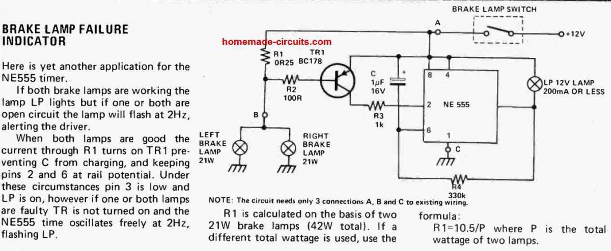 When both the rear lamps work in a sound condition, the current passing by means of R1 activates TR1 blocking capacitor C from charging, which allows the pins 2 and 6 at the supply potential.
In these situations pin 3 of the IC is held low which keeps lamp Lp illuminated.
On the other hand if a single or the two lamps become faulty TR does not get switched on, which allows the NE555 IC to oscillates continuously at 2Hz, causing the lamp LP to flash.
When both the rear lamps work in a sound condition, the current passing by means of R1 activates TR1 blocking capacitor C from charging, which allows the pins 2 and 6 at the supply potential.
In these situations pin 3 of the IC is held low which keeps lamp Lp illuminated.
On the other hand if a single or the two lamps become faulty TR does not get switched on, which allows the NE555 IC to oscillates continuously at 2Hz, causing the lamp LP to flash.
 A low logic signal on the latch-enable input pin 5 (LE) of IC2 latches the count in the counter module into the on chip set output latches.
In an event when switch S2 is switched ON, pin 5 is forced to go low and thereby the count figure is allowed to be saved in the latch section of the IC.
Display-select pin 6 (DS) ascertains if the figure on the counter or the stored count in the latch may be shown on the display or not.
In case pin 6 is held low the figure in the output latch section is enabled to get displayed, however if pin 6 is rendered with a high logic the count stored in the counter is illuminated over the connected display.
On an occasion when switch S2 is switched, the base of pnp transistor T2 is linked with ground ensuring that it begins operating.
The emitter of T2 is rigged with DS pin of IC2.
Consequently, whenever switch S3 is switched ON, reset pin 13 of IC2 is coupled with negative through the transistor T1 making sure that the oscillator is inhibited from generating clock pulses.
This operation is executed to implement a synchronization between IC1 and IC2.
At the first level, reset the module in order to enable the display to show ¡®0000.¡¯ Next disconnect switch S2 for the stop watch to initiate its counting the periods.
In case you wished to inhibit the clocking of the chip, simply switch OFF the control S2.
The given rotary switch S1 may be opted for selecting the many different time intervals at the output of the astable multivibrator (IC1).
The proposed digital stopwatch circuit will work off a 5V supply inputs.
The circuit may be easily fixed and built on a general-purpose PCB.
You may want to enclose the entire circuit in a metallic cabinet with slots built for four 7-segment displays, rotary switch S1, start/stop switch S2 and reset switch S3 in the dashboard plate of the selected encloser.
A low logic signal on the latch-enable input pin 5 (LE) of IC2 latches the count in the counter module into the on chip set output latches.
In an event when switch S2 is switched ON, pin 5 is forced to go low and thereby the count figure is allowed to be saved in the latch section of the IC.
Display-select pin 6 (DS) ascertains if the figure on the counter or the stored count in the latch may be shown on the display or not.
In case pin 6 is held low the figure in the output latch section is enabled to get displayed, however if pin 6 is rendered with a high logic the count stored in the counter is illuminated over the connected display.
On an occasion when switch S2 is switched, the base of pnp transistor T2 is linked with ground ensuring that it begins operating.
The emitter of T2 is rigged with DS pin of IC2.
Consequently, whenever switch S3 is switched ON, reset pin 13 of IC2 is coupled with negative through the transistor T1 making sure that the oscillator is inhibited from generating clock pulses.
This operation is executed to implement a synchronization between IC1 and IC2.
At the first level, reset the module in order to enable the display to show ¡®0000.¡¯ Next disconnect switch S2 for the stop watch to initiate its counting the periods.
In case you wished to inhibit the clocking of the chip, simply switch OFF the control S2.
The given rotary switch S1 may be opted for selecting the many different time intervals at the output of the astable multivibrator (IC1).
The proposed digital stopwatch circuit will work off a 5V supply inputs.
The circuit may be easily fixed and built on a general-purpose PCB.
You may want to enclose the entire circuit in a metallic cabinet with slots built for four 7-segment displays, rotary switch S1, start/stop switch S2 and reset switch S3 in the dashboard plate of the selected encloser.
 It's invented by an Australian person named Bronte EcKermann and created by South Australian manufacturer Zing International.
It is said that the cost of these stumps may be as high as US$ 40,000 for each set, gosh!.
The circuit of these LED stumps is assumed to be consisting of all sorts of complex designs using microcontrollers.
In this article we'll learn how each of these circuits can be built using ordinary components at less than $5 and yet be as effective as the original LED stump specs.
It's invented by an Australian person named Bronte EcKermann and created by South Australian manufacturer Zing International.
It is said that the cost of these stumps may be as high as US$ 40,000 for each set, gosh!.
The circuit of these LED stumps is assumed to be consisting of all sorts of complex designs using microcontrollers.
In this article we'll learn how each of these circuits can be built using ordinary components at less than $5 and yet be as effective as the original LED stump specs.
 The IC1 which is an IC 555 is configured as a monostable wherein R3 and C2 along with R4 decides the ON time of the LEDs.
An NPN transistor T1 can be seen attached with pin2 trigger input of the IC, whose base is rigged with a couple of reed switches in series.
The idea is simple: The entire circuit is required to be fixed inside each of the bails with the reed switches enclosed inside the end tubes of the bails.
Furthermore, a permanent magnet needs to be fixed at the upper ends of the stumps so that the reed switches remain closed for so long as these are held over the stumps.
The IC1 which is an IC 555 is configured as a monostable wherein R3 and C2 along with R4 decides the ON time of the LEDs.
An NPN transistor T1 can be seen attached with pin2 trigger input of the IC, whose base is rigged with a couple of reed switches in series.
The idea is simple: The entire circuit is required to be fixed inside each of the bails with the reed switches enclosed inside the end tubes of the bails.
Furthermore, a permanent magnet needs to be fixed at the upper ends of the stumps so that the reed switches remain closed for so long as these are held over the stumps.
 The figure above shows how the magnets inside the stumps needs to be embedded and positioned for the bails to respond to these.
As long as the bails are held over the stumps, the reed switches stay closed ensuring a switched OFF T1. However the moment the bail is completely dislodged from the slots, allows the reed switches to open and switch ON T1 which in turn triggers the monostable illuminating the LEDs for a time period as determined by R3/R4/C2. The LEDs remain shut off until these are yet again positioned over the stumps for a repetition.
That takes care of the bail circuitry, pretty simple....
isn't that?
In the above diagram we can also see LDRs being positioned right at the top of the stumps just under small apertures that my be drilled on top surfaces of the stumps.
These LDRs become exposed to the ambient external light the moment the bails are dislodged from the slots.
since these LDrs are supposed to be integrated with sets of identical monostables inside the stumps, the operation becomes responsible for illuminating the LEDs attached on the stumps, thus the entire system consisting of the stumps and the bails become synchronized providing a foolproof sequence of the proceedings.
UPDATE:
Hey friends, today I made the LED bail design even simpler by using transistors instead of an IC.
The advantage of this circuit is that it can work even with a 3 V supply and also blink the connected LEDs during its ON period.
Additionally, I have ensured that the standy current of the circuit is negligibly low (while these are mounted on the stumps)
Here's the new circuit diagram for your viewing pleasure!
The figure above shows how the magnets inside the stumps needs to be embedded and positioned for the bails to respond to these.
As long as the bails are held over the stumps, the reed switches stay closed ensuring a switched OFF T1. However the moment the bail is completely dislodged from the slots, allows the reed switches to open and switch ON T1 which in turn triggers the monostable illuminating the LEDs for a time period as determined by R3/R4/C2. The LEDs remain shut off until these are yet again positioned over the stumps for a repetition.
That takes care of the bail circuitry, pretty simple....
isn't that?
In the above diagram we can also see LDRs being positioned right at the top of the stumps just under small apertures that my be drilled on top surfaces of the stumps.
These LDRs become exposed to the ambient external light the moment the bails are dislodged from the slots.
since these LDrs are supposed to be integrated with sets of identical monostables inside the stumps, the operation becomes responsible for illuminating the LEDs attached on the stumps, thus the entire system consisting of the stumps and the bails become synchronized providing a foolproof sequence of the proceedings.
UPDATE:
Hey friends, today I made the LED bail design even simpler by using transistors instead of an IC.
The advantage of this circuit is that it can work even with a 3 V supply and also blink the connected LEDs during its ON period.
Additionally, I have ensured that the standy current of the circuit is negligibly low (while these are mounted on the stumps)
Here's the new circuit diagram for your viewing pleasure!
 Important: Please keep both the reed switches together on a single arm of the bail and linked with a single magnet on the stump, instead of installing them across the opposite arms of the bail.
Because both the reed switches need to close while they are placed on the stumps, if one of the reed is open then the circuit might not respond correctly.
Video Proof or the Test Results of the above LED Bail
Parts List
R1, R4 = 100 Ohms
R2, R3 = 56K
R5, R6 = 10K
R7 = 330K
C1, C2 = 10uF/6V
C3 = 1000uF/6V
T1, T2, T3 = BC547
T4 = BC557
Miscellaneous = Reed Relay switches, 3V Button Cell
The above LED Bail circuit can be further simplified by using a vibration switch, as shown below, although I doubt the accuracy level may not be as good as the reed relay version.
Important: Please keep both the reed switches together on a single arm of the bail and linked with a single magnet on the stump, instead of installing them across the opposite arms of the bail.
Because both the reed switches need to close while they are placed on the stumps, if one of the reed is open then the circuit might not respond correctly.
Video Proof or the Test Results of the above LED Bail
Parts List
R1, R4 = 100 Ohms
R2, R3 = 56K
R5, R6 = 10K
R7 = 330K
C1, C2 = 10uF/6V
C3 = 1000uF/6V
T1, T2, T3 = BC547
T4 = BC557
Miscellaneous = Reed Relay switches, 3V Button Cell
The above LED Bail circuit can be further simplified by using a vibration switch, as shown below, although I doubt the accuracy level may not be as good as the reed relay version.
 In the diagram we are able to witness the integration methods of the LDRs with a 555 IC based monostable.
As long as the bails are held over the stumps, the ambient light stay blocked from the LDRs which keeps T1 switched OFF.
but the moment the bails are thrown of the stumps, the LDRs become exposed to the ambient light enabling T1 to receive a biasing voltage which in turn triggers the monostable so that the LEDs are illuminated for the set period of time fixed by the relevant components.
The LEDs shut of after the set time has elapsed until the bails are restored over the stumps for yet another cycle.
Designed by: Swagatam.
In the diagram we are able to witness the integration methods of the LDRs with a 555 IC based monostable.
As long as the bails are held over the stumps, the ambient light stay blocked from the LDRs which keeps T1 switched OFF.
but the moment the bails are thrown of the stumps, the LDRs become exposed to the ambient light enabling T1 to receive a biasing voltage which in turn triggers the monostable so that the LEDs are illuminated for the set period of time fixed by the relevant components.
The LEDs shut of after the set time has elapsed until the bails are restored over the stumps for yet another cycle.
Designed by: Swagatam.
 Note: In the explanation of the circuit, it is proposed to be fed with 12 volts, however it may work well even with a voltage range from 5-15 volts.
One can use a 9 volt battery PP3, and thus have a much portable circuit.
IC 555 pinout
Note: In the explanation of the circuit, it is proposed to be fed with 12 volts, however it may work well even with a voltage range from 5-15 volts.
One can use a 9 volt battery PP3, and thus have a much portable circuit.
IC 555 pinout
 Both the circuits can be used for any application that requires a uniquely tuned infrared detection such as in IR remote control, IR security systems or IR based lock and key devices.
The first circuit utilizes a LM567 phase locked loop frequency detector chip to form the receiver circuit.
R2/R3/C2 fix the latching frequency for the IC such that the circuit responds and creates a zero logic output on detection of this frequency at its input pin3 via the photodiode.
The photdiode is triggered by a 555 based astable circuit shown at the left of the diagrams.
The 555 circuit also employs a photo diode for transmitting the frequency over the receiving LM567 photo diode device.
The 555 transmitter must be tuned exactly to the frequency which is set with R2/R3/C2 in the LM567 circuit.
Anything else is simply ignored by the Rx circuit.
In the second tuned infrared detector circuit, an LC tuned opamp is employed for receiving an responding to the uniquely tuned transmitter frequency.
Both the circuits can be used for any application that requires a uniquely tuned infrared detection such as in IR remote control, IR security systems or IR based lock and key devices.
The first circuit utilizes a LM567 phase locked loop frequency detector chip to form the receiver circuit.
R2/R3/C2 fix the latching frequency for the IC such that the circuit responds and creates a zero logic output on detection of this frequency at its input pin3 via the photodiode.
The photdiode is triggered by a 555 based astable circuit shown at the left of the diagrams.
The 555 circuit also employs a photo diode for transmitting the frequency over the receiving LM567 photo diode device.
The 555 transmitter must be tuned exactly to the frequency which is set with R2/R3/C2 in the LM567 circuit.
Anything else is simply ignored by the Rx circuit.
In the second tuned infrared detector circuit, an LC tuned opamp is employed for receiving an responding to the uniquely tuned transmitter frequency.
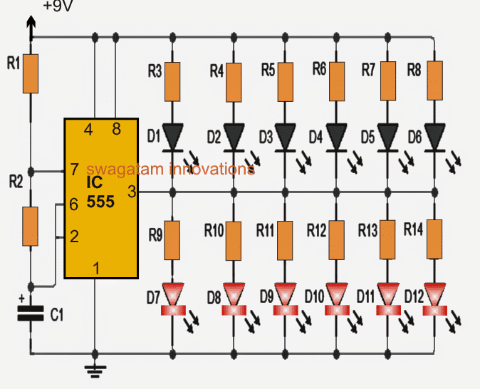 Parts list for the discussed bicycle safety light
IC1: 555 timer
D1 through D12: red LEDs 5mm
R1: 10K resistor
R2: 100K resistor
R3 to R14: 1K 1/4 watt
C1: 10uF/25V
Parts list for the discussed bicycle safety light
IC1: 555 timer
D1 through D12: red LEDs 5mm
R1: 10K resistor
R2: 100K resistor
R3 to R14: 1K 1/4 watt
C1: 10uF/25V
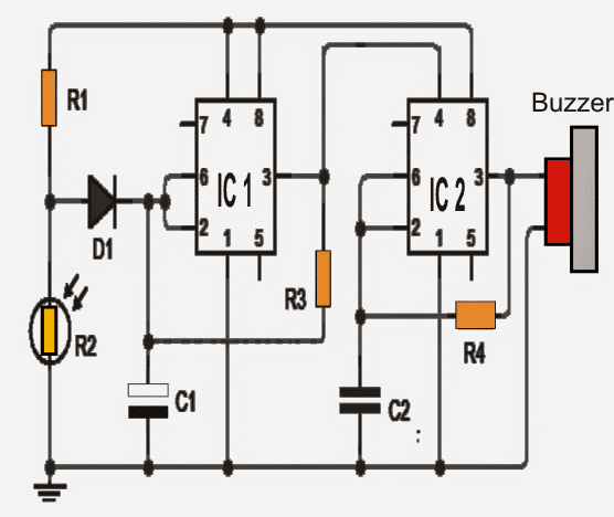

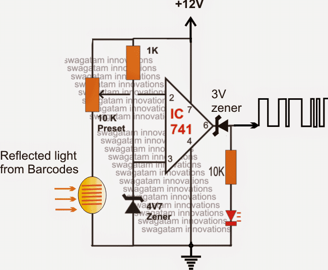
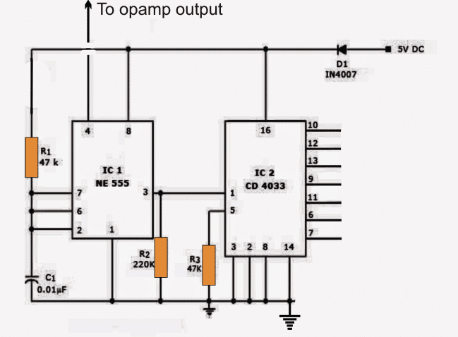
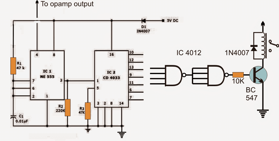 A 4 input NAND gate IC 4012 could be used and configured with any four selected unique outputs of the decoder for activating a security relay.
If 3 high outputs are selected then one of the NAND inputs could be shorted to the positive supply.
A 4 input NAND gate IC 4012 could be used and configured with any four selected unique outputs of the decoder for activating a security relay.
If 3 high outputs are selected then one of the NAND inputs could be shorted to the positive supply.
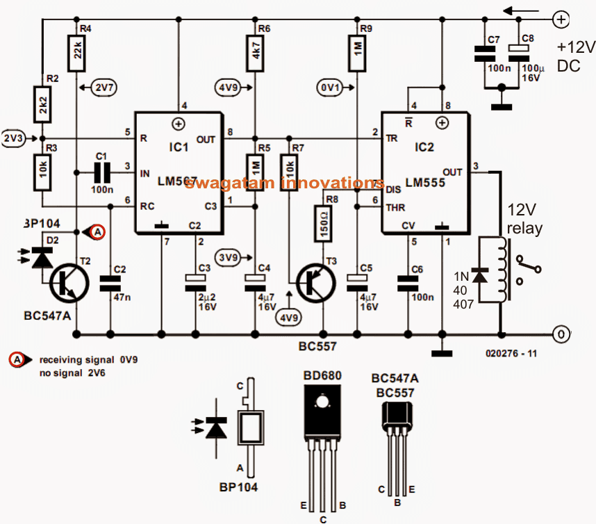
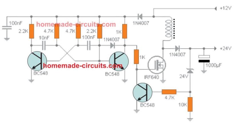 All the shown parts are standard, or could be replaced with other suitable equivalents.
The inductor which is one of main parts of the circuit is built over a ferrite rod 1 cm in diameter, by winding 100 turns of super enameled copper wire having 1 mm thickness.
Actually, the inductor is dependent on the frequency of the transistor astable.
For higher frequencies the number of turns will proportionately go down, and is a matter of some experimentation.
The turn number will also depend on the ferrite core shape, and may significantly decrease if a ring type ferrite core is used.
All the shown parts are standard, or could be replaced with other suitable equivalents.
The inductor which is one of main parts of the circuit is built over a ferrite rod 1 cm in diameter, by winding 100 turns of super enameled copper wire having 1 mm thickness.
Actually, the inductor is dependent on the frequency of the transistor astable.
For higher frequencies the number of turns will proportionately go down, and is a matter of some experimentation.
The turn number will also depend on the ferrite core shape, and may significantly decrease if a ring type ferrite core is used.
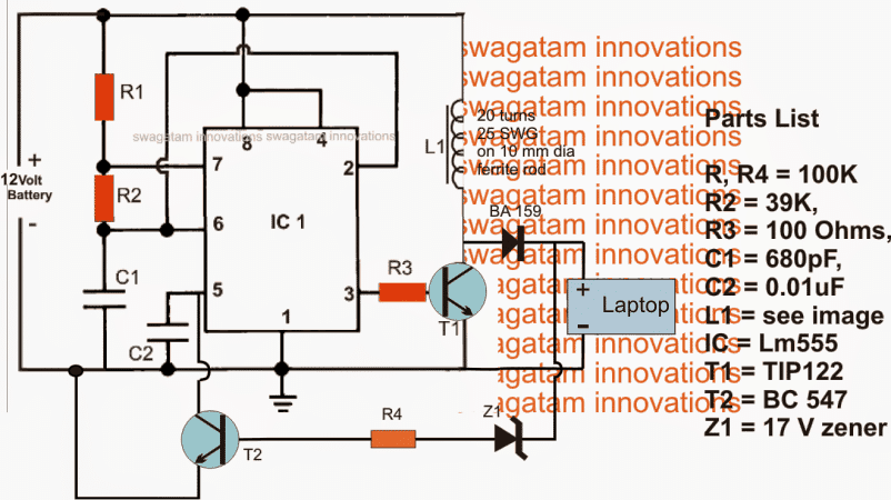 The various stages included in the above 12 V laptop boost charger circuit may be understood as follows:
IC1 which is a 555 IC is configured as a standard astable for generating a stable predetermined frequency at the rate of 12 kHz which is acquired at pin3 of the IC.
The above high frequency output is fed to the base of a driver BJT T1 for inducing the above frequency with high current in L1.
Due to the inherent property of the inductor L1, during every OFF time of T1, an equivalent amount of boosted voltage is kicked back from the inductor L1 and supplied to the load connected at the output via the fast recovery diode BA159.
The load here is the laptop which accepts the boosted voltage for charging its internal battery.
Since the laptop may require a precise 19 to 20V for the operations, the output from L1 must be regulated and stabilized in order to make things safe for the connected laptop battery.
The above criterion is taken care of by introducing T2 and the associated R4 and Z1 components.
Z1 is selected to be exactly equal to the laptop charging voltage that is at 20 V (17V is wrongly shown in the diagram).
Whenever the output tends to drift away from this value, Z1 gets forward biased triggering T2, which in turn grounds pin5 of the IC.
The above situation immediately reduces the IC 555 pin3 voltage to minimal levels for that instant until Z1 stops conducting and the situation is restored to the safe zone....the switching is sustained at a rapid speed maintaining a constant voltage for the laptop.
This car laptop charger circuit can be used for charging a laptop in any car which uses a 12V battery.
The various stages included in the above 12 V laptop boost charger circuit may be understood as follows:
IC1 which is a 555 IC is configured as a standard astable for generating a stable predetermined frequency at the rate of 12 kHz which is acquired at pin3 of the IC.
The above high frequency output is fed to the base of a driver BJT T1 for inducing the above frequency with high current in L1.
Due to the inherent property of the inductor L1, during every OFF time of T1, an equivalent amount of boosted voltage is kicked back from the inductor L1 and supplied to the load connected at the output via the fast recovery diode BA159.
The load here is the laptop which accepts the boosted voltage for charging its internal battery.
Since the laptop may require a precise 19 to 20V for the operations, the output from L1 must be regulated and stabilized in order to make things safe for the connected laptop battery.
The above criterion is taken care of by introducing T2 and the associated R4 and Z1 components.
Z1 is selected to be exactly equal to the laptop charging voltage that is at 20 V (17V is wrongly shown in the diagram).
Whenever the output tends to drift away from this value, Z1 gets forward biased triggering T2, which in turn grounds pin5 of the IC.
The above situation immediately reduces the IC 555 pin3 voltage to minimal levels for that instant until Z1 stops conducting and the situation is restored to the safe zone....the switching is sustained at a rapid speed maintaining a constant voltage for the laptop.
This car laptop charger circuit can be used for charging a laptop in any car which uses a 12V battery.
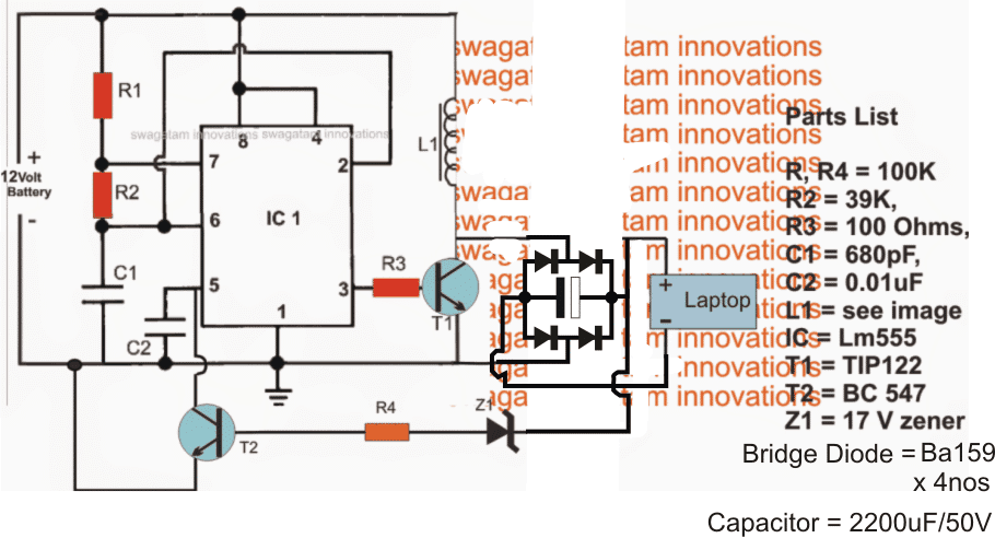
 A novel little circuit presented here will allow a laptop battery to be charged even from a DC source such as a car or truck batteries (12V).
It's a very simple, cheap, versatile and universal circuit which may be dimensioned for charging all types of laptops by adjusting the relevant components provided in the circuit.
It's a simple plug and play charger circuit.
Normally most of the laptop adapters are rated at 19V/3.5Amps, however some may be rated at higher currents for facilitating fast charging.
A novel little circuit presented here will allow a laptop battery to be charged even from a DC source such as a car or truck batteries (12V).
It's a very simple, cheap, versatile and universal circuit which may be dimensioned for charging all types of laptops by adjusting the relevant components provided in the circuit.
It's a simple plug and play charger circuit.
Normally most of the laptop adapters are rated at 19V/3.5Amps, however some may be rated at higher currents for facilitating fast charging.
 The circuit is based on a simple IC 4017 and IC 555 sequential dot mode driver circuit.
The output of the IC 4017 create a running or sequencing high logic pulse across its 10 outputs in response to the clocks generated by the IC 555 astable at its pin#14. Each of these outputs are configured across a transistor/inductor circuit which act like a small boost converters, and convert the 9V pulse into a low current 100V or 120V short pulses.
The indicated ends could be integrated with 10 individual needles for the required transcutaneous stimulation across the intended muscle areas.
The pulse width and frequency can be controlled by adjusting the 100k preset.
Warning: The coil dimension and voltage presented above are assumed values only, and have not been confirmed.
Serious experimentation may be required through qualified medical engineers before implementing the device practically.
The circuit is based on a simple IC 4017 and IC 555 sequential dot mode driver circuit.
The output of the IC 4017 create a running or sequencing high logic pulse across its 10 outputs in response to the clocks generated by the IC 555 astable at its pin#14. Each of these outputs are configured across a transistor/inductor circuit which act like a small boost converters, and convert the 9V pulse into a low current 100V or 120V short pulses.
The indicated ends could be integrated with 10 individual needles for the required transcutaneous stimulation across the intended muscle areas.
The pulse width and frequency can be controlled by adjusting the 100k preset.
Warning: The coil dimension and voltage presented above are assumed values only, and have not been confirmed.
Serious experimentation may be required through qualified medical engineers before implementing the device practically.
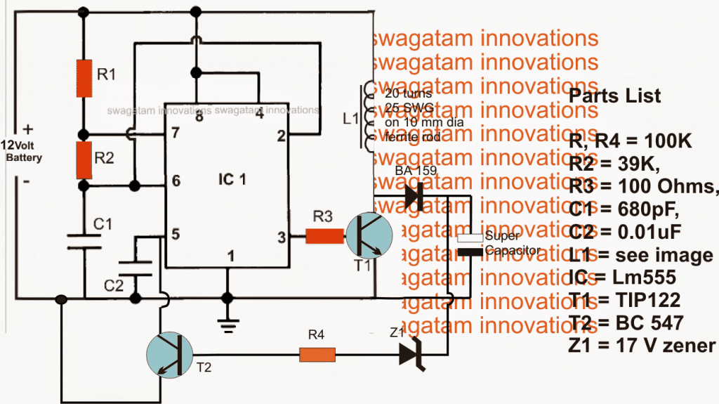
 Note: Please connect a 1K resistor across pin5 and ground of IC2 for correct functioning of the circuit.
The proposed self optimizing solar battery charger circuit with buck converter circuit may be grasped with the help of the following explanation:
The circuit consists of three basic stages viz: the PWM solar voltage optimizer using couple of IC 555s in the the form of IC1 and IC2, the mosfet PWM current amplifier and the buck converter using L1 and the associated components.
IC1 is rigged to produce a frequency of about 80 Hz while IC2 is configured as a comparator and PWM generator.
The 80 Hz from IC 1 is fed to pin2 of IC2 which utilizes this frequency for manufacturing triangle waves across C1....
which are further compared with the instantaneous potentials at its pin5 for dimensioning the correct PWMs at its pin3.
The pin5 potential as may be seen in the diagram, is derived from the solar panel through a potential divider stage and a BJT common collector stgae.
The preset positioned with this potential divider is initially appropriately adjusted such that at the peak solar panel voltage the output from the buck converter produces the optimal magnitude of voltage suiting the connected battery's charging level.
Once the above is set rest is handled automatically by the IC1/IC2 stage.
During peak sunlight the PWMs get appropriately shortened ensuring minimum stress on the solar panel yet producing the correct optimal voltage for the battery due to the presence of the buck converter stage (a buck boost type of design is the most efficient method of reducing a voltage source without stressing the source parameters)
Now, as the sun light begins diminishing the voltage across the set potential divider also begins to drop proportionately which is detected at pin5 of IC2....on detecting this gradual deterioration of the sample voltage IC2 begins widening the PWMs so that the buck output is able to maintain the required optimal battery charging voltage, this implies that the battery continues to receive the correct amount of power regardless of the sun's retarding illumination.
L1 should be dimensioned appropriately such that it generates the approximate optimal voltage level for the battery when the solar panel is at its peak specification or in other words when the sunlight is in the most favorable position for the solar panel.
RX is introduced for determining and restricting the maximum charging current limit for the battery, it may calculated with the help of the following formula:
Rx = 0.7 x 10 / Battery AH
Note: Please connect a 1K resistor across pin5 and ground of IC2 for correct functioning of the circuit.
The proposed self optimizing solar battery charger circuit with buck converter circuit may be grasped with the help of the following explanation:
The circuit consists of three basic stages viz: the PWM solar voltage optimizer using couple of IC 555s in the the form of IC1 and IC2, the mosfet PWM current amplifier and the buck converter using L1 and the associated components.
IC1 is rigged to produce a frequency of about 80 Hz while IC2 is configured as a comparator and PWM generator.
The 80 Hz from IC 1 is fed to pin2 of IC2 which utilizes this frequency for manufacturing triangle waves across C1....
which are further compared with the instantaneous potentials at its pin5 for dimensioning the correct PWMs at its pin3.
The pin5 potential as may be seen in the diagram, is derived from the solar panel through a potential divider stage and a BJT common collector stgae.
The preset positioned with this potential divider is initially appropriately adjusted such that at the peak solar panel voltage the output from the buck converter produces the optimal magnitude of voltage suiting the connected battery's charging level.
Once the above is set rest is handled automatically by the IC1/IC2 stage.
During peak sunlight the PWMs get appropriately shortened ensuring minimum stress on the solar panel yet producing the correct optimal voltage for the battery due to the presence of the buck converter stage (a buck boost type of design is the most efficient method of reducing a voltage source without stressing the source parameters)
Now, as the sun light begins diminishing the voltage across the set potential divider also begins to drop proportionately which is detected at pin5 of IC2....on detecting this gradual deterioration of the sample voltage IC2 begins widening the PWMs so that the buck output is able to maintain the required optimal battery charging voltage, this implies that the battery continues to receive the correct amount of power regardless of the sun's retarding illumination.
L1 should be dimensioned appropriately such that it generates the approximate optimal voltage level for the battery when the solar panel is at its peak specification or in other words when the sunlight is in the most favorable position for the solar panel.
RX is introduced for determining and restricting the maximum charging current limit for the battery, it may calculated with the help of the following formula:
Rx = 0.7 x 10 / Battery AH
 In the above updated design I have made the following important change:
I have added a NPN inverter at pin3 of IC 2 so that now the PWMs from IC 2 influences the mosfet to extract maximum power from the panel and reduces the power gradually as the sun light diminishes.
The PWM pulses along with the buck converter guarantees a perfect compatibility and maximum power extraction from the panel, but diminishes gradually in response to the sun's diminishing intensity.
However, the above set up makes sure about one important aspect, it ensures a balanced input/output power ratio which is always a key issue in MPPT chargers.
Further if in case the load tries to extract an excessive amount of current, the BC557 current limiter immediately comes into action preventing the disruption of the smooth functioning of the MPPT by cutting off power to the load during those periods.
Update
In the above updated design I have made the following important change:
I have added a NPN inverter at pin3 of IC 2 so that now the PWMs from IC 2 influences the mosfet to extract maximum power from the panel and reduces the power gradually as the sun light diminishes.
The PWM pulses along with the buck converter guarantees a perfect compatibility and maximum power extraction from the panel, but diminishes gradually in response to the sun's diminishing intensity.
However, the above set up makes sure about one important aspect, it ensures a balanced input/output power ratio which is always a key issue in MPPT chargers.
Further if in case the load tries to extract an excessive amount of current, the BC557 current limiter immediately comes into action preventing the disruption of the smooth functioning of the MPPT by cutting off power to the load during those periods.
Update
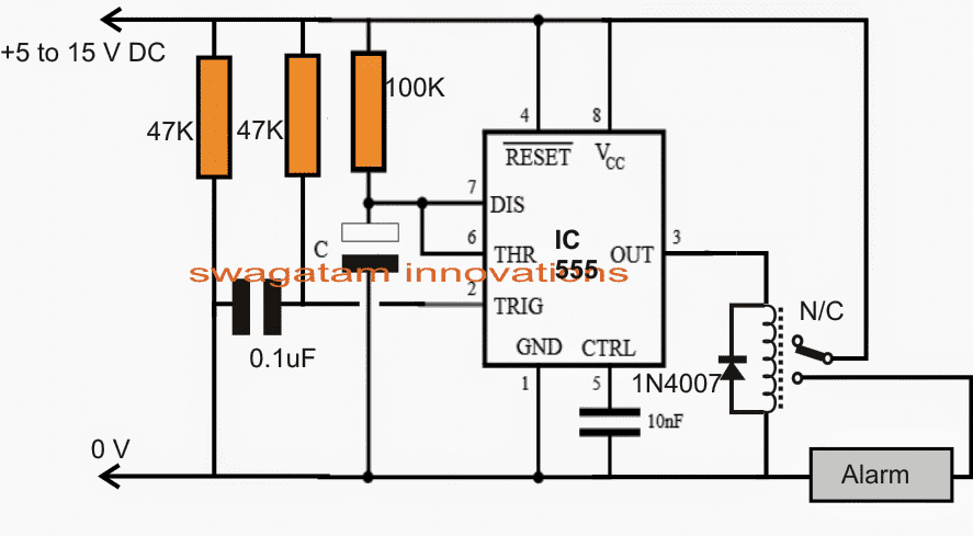
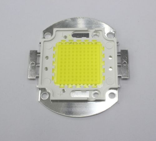 For the driver I'm looking at one of the following:
 or
or
 or
or
 I need the driver to boost/step up voltage from 11-13v to the required voltage of the LED module, and in this case that would be 30-36V and of course be able to current limit the output.
But what I also want, that none of the drivers listed above provides is being able to dim, or set maybe 3 to 5 different intensities like 10%, 30%, 50%, 70% and 100%.
I would also like the driver and on/off-function to could be controlled by a reed/magnet switch to avoid running a switch through the watertight casing.
Keeping the size down is also beneficial.
Is there any way you would think it is possible to modify the drivers listed? Or is it possible to build something like this by myself?
If you do have the time to consider a circuit like this it could be very helpful.
I am planning to have two separate light heads with one 100W LED SMD in each, and run them from the same battery.
It is for video lights, so one light on each side of the camera.
If the control of these two lights could be controlled by the same switch it would be nice also
Great site btw, thank you for sharing all your information!
Kind regards,
Svein
I need the driver to boost/step up voltage from 11-13v to the required voltage of the LED module, and in this case that would be 30-36V and of course be able to current limit the output.
But what I also want, that none of the drivers listed above provides is being able to dim, or set maybe 3 to 5 different intensities like 10%, 30%, 50%, 70% and 100%.
I would also like the driver and on/off-function to could be controlled by a reed/magnet switch to avoid running a switch through the watertight casing.
Keeping the size down is also beneficial.
Is there any way you would think it is possible to modify the drivers listed? Or is it possible to build something like this by myself?
If you do have the time to consider a circuit like this it could be very helpful.
I am planning to have two separate light heads with one 100W LED SMD in each, and run them from the same battery.
It is for video lights, so one light on each side of the camera.
If the control of these two lights could be controlled by the same switch it would be nice also
Great site btw, thank you for sharing all your information!
Kind regards,
Svein
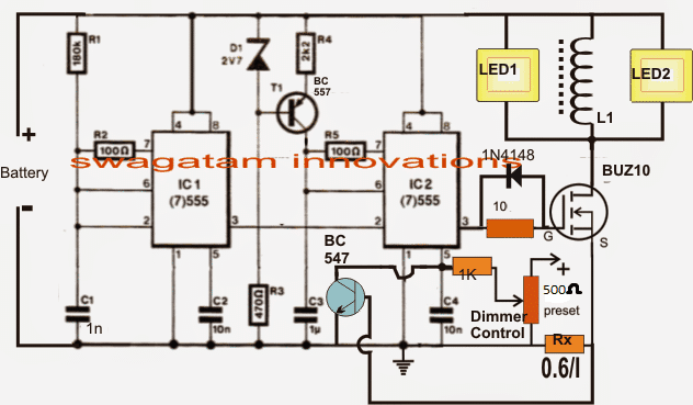
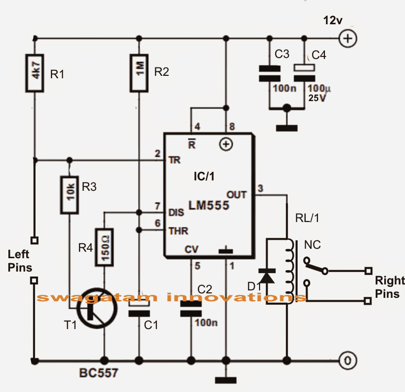 IC 555 pinout Specs
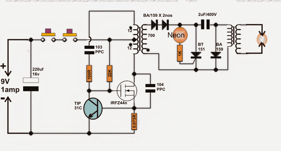
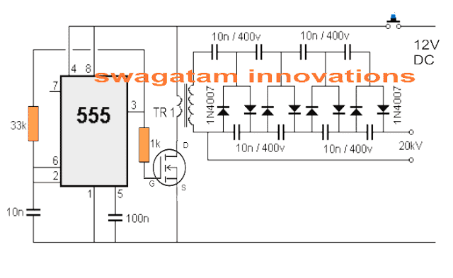
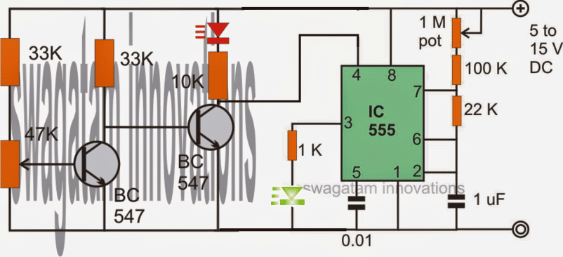
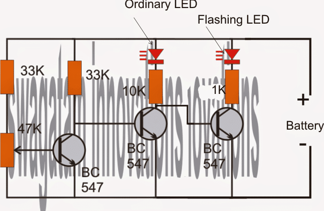
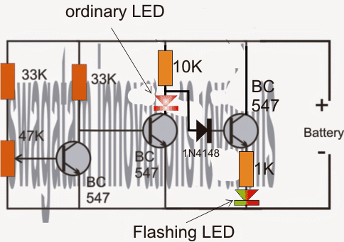
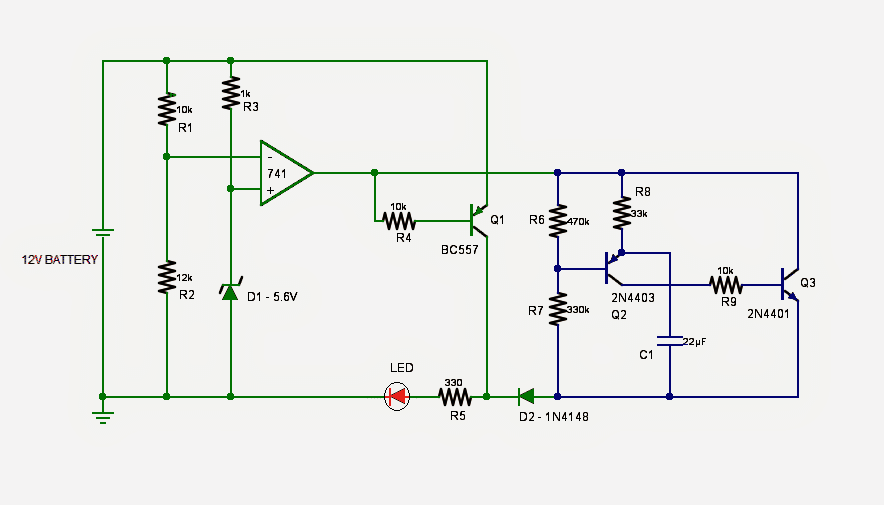 The circuit presented here features a single LED which:
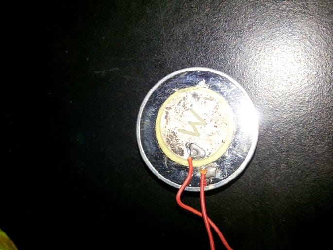
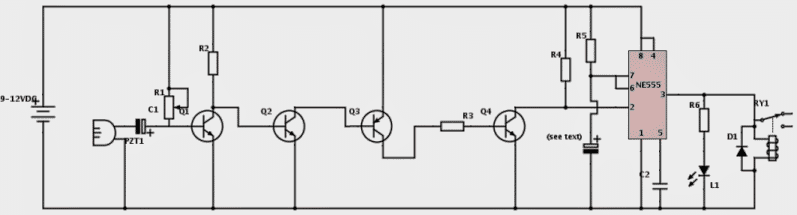 Written and Submitted by: SS kopparthy
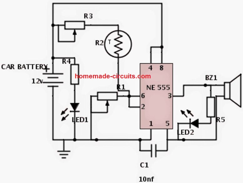
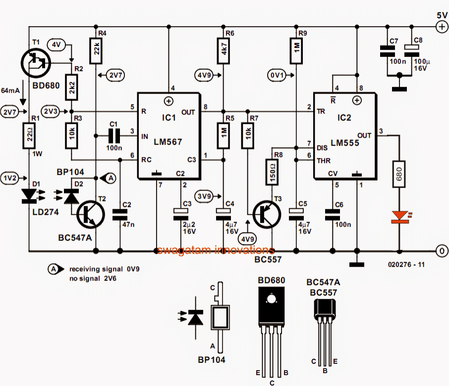
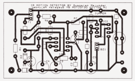
 IC 555 Pinout

 The circuit diagram for the Switching Amplifier can be seen in the above image.
An independent 51 V DC supply is necessary to energize the Amplifier circuit.
The 51 V supply source is applied to a set of Zener diodes, D5 and D6, and it is smoothed through capacitors C11 and C12 in order to get a 12 V DC source for the amplifier circuit.
Additionally, portion of the 51 V DC source overrides the Zeners to supply the stages of the circuit which are supposed to work with 51 V DC directly.
The circuit diagram for the Switching Amplifier can be seen in the above image.
An independent 51 V DC supply is necessary to energize the Amplifier circuit.
The 51 V supply source is applied to a set of Zener diodes, D5 and D6, and it is smoothed through capacitors C11 and C12 in order to get a 12 V DC source for the amplifier circuit.
Additionally, portion of the 51 V DC source overrides the Zeners to supply the stages of the circuit which are supposed to work with 51 V DC directly.
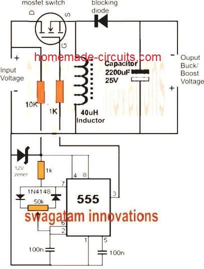 The above design can be suitably upgraded for implementing an automatic output voltage correction with the help of the following modifications:
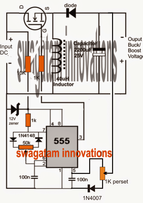 The 1K preset may be appropriately set initially for determining the desired control point.
IC 555 Pinouts
The 1K preset may be appropriately set initially for determining the desired control point.
IC 555 Pinouts
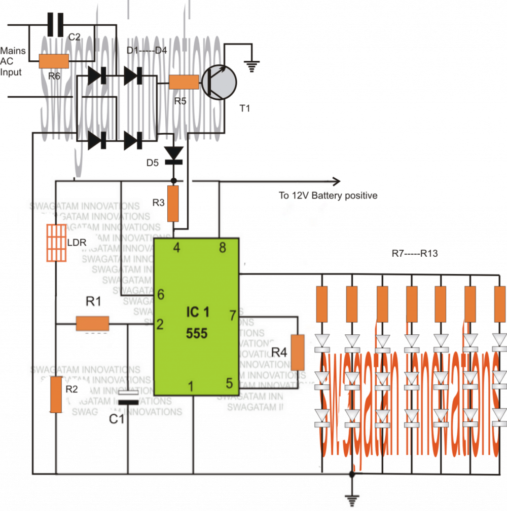
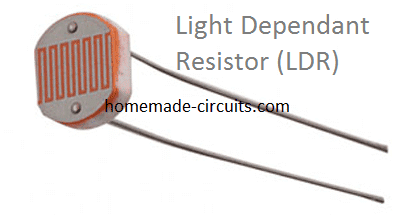
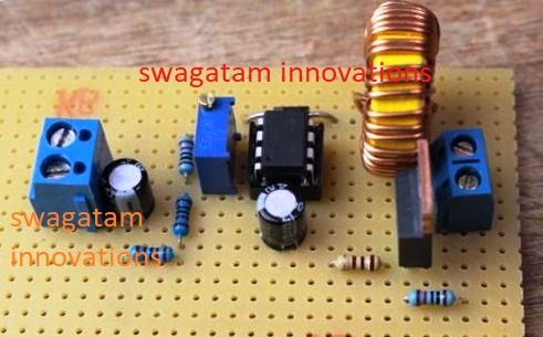
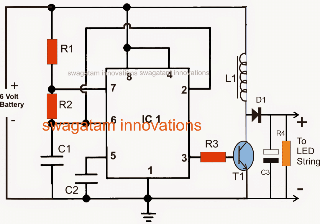
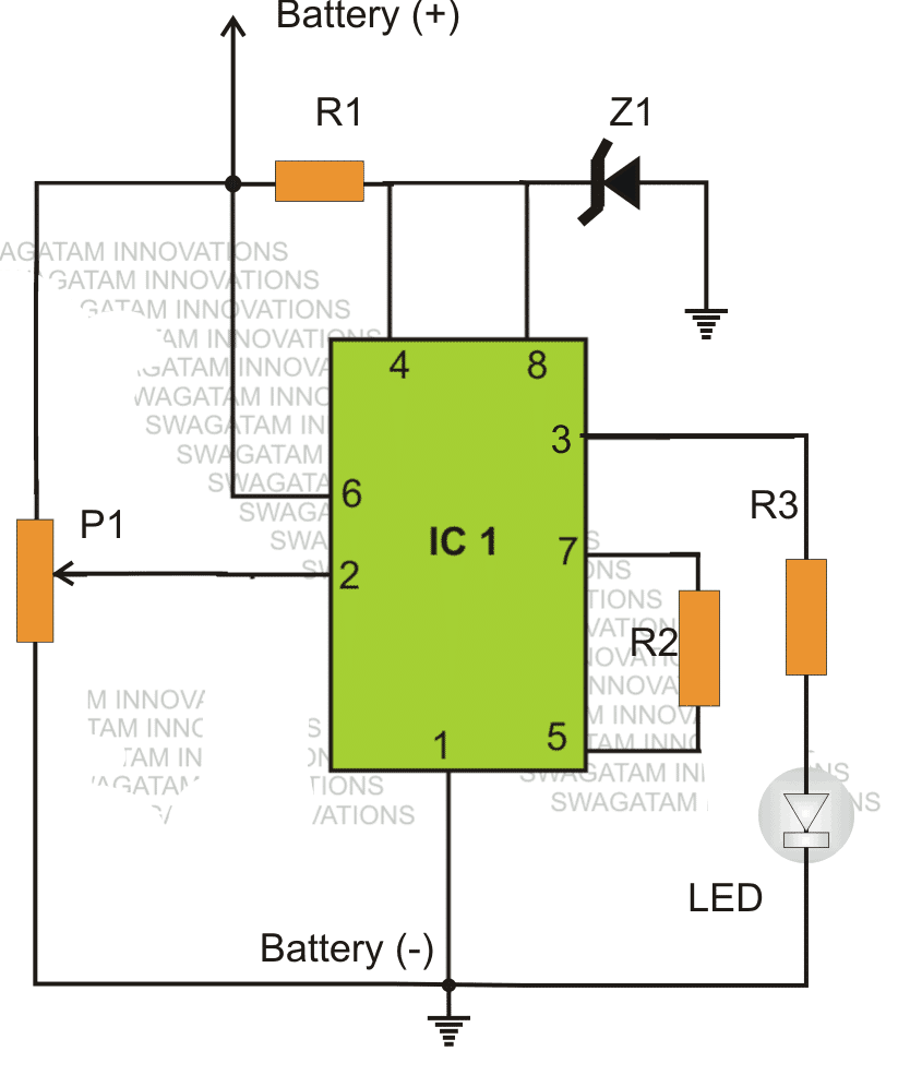
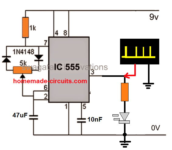
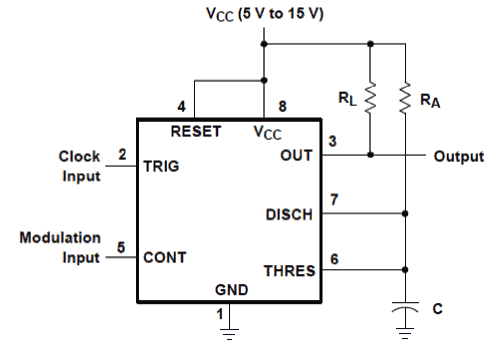 IC 555 Pinout
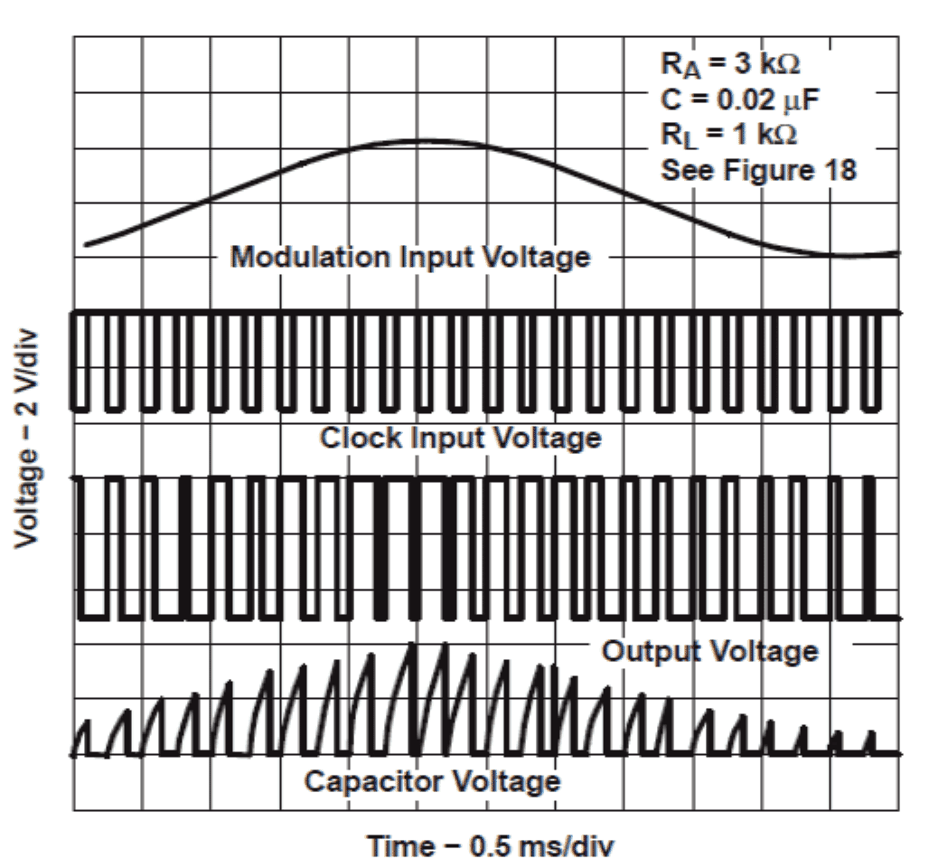 The topmost waveform represents the modulation voltage at pin#5, the bulge in the waveform represents the rising voltage and vice versa.
The second waveform represents the uniform clock pulse applied at pin#2. It's just for enabling the IC to switch at a certain frequency, without which the IC wouldn't be able to work as a PWM generator device.
The third waveform depicts the actual PWM generation at pin#3, we can see that the width of the pulses is directly proportional to the top modulation signal.
The pulse widths corresponding to the "bulge" can be seen as much wider and closely spaced which proportionately becomes thinner and sparse withthefall in the modulation voltage level.
The above concept can be very easily and effectively applied in power control applications as discussed earlier in the above article.
The topmost waveform represents the modulation voltage at pin#5, the bulge in the waveform represents the rising voltage and vice versa.
The second waveform represents the uniform clock pulse applied at pin#2. It's just for enabling the IC to switch at a certain frequency, without which the IC wouldn't be able to work as a PWM generator device.
The third waveform depicts the actual PWM generation at pin#3, we can see that the width of the pulses is directly proportional to the top modulation signal.
The pulse widths corresponding to the "bulge" can be seen as much wider and closely spaced which proportionately becomes thinner and sparse withthefall in the modulation voltage level.
The above concept can be very easily and effectively applied in power control applications as discussed earlier in the above article.
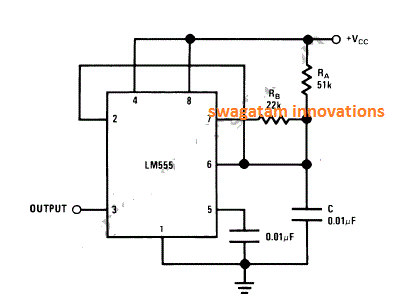
 Note: Please connect the buzzer or the load between pin#3 and ground, and not between pin#3 and positive as incorrectly shown in the above diagram.
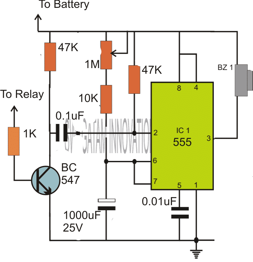 Please connect the buzzer or the load between pin#3 and ground, and not between pin#3 and positive as incorrectly shown in the above diagram.
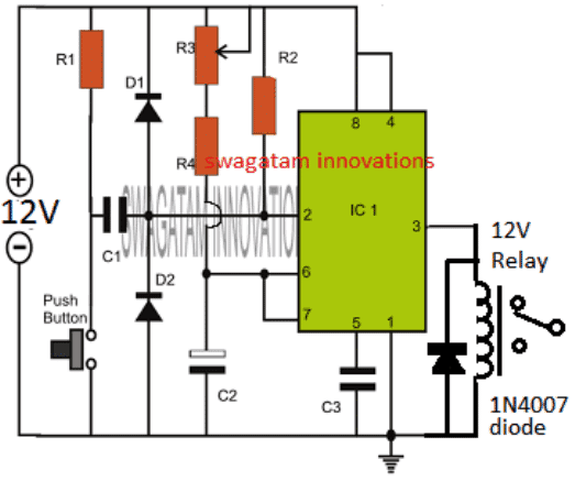
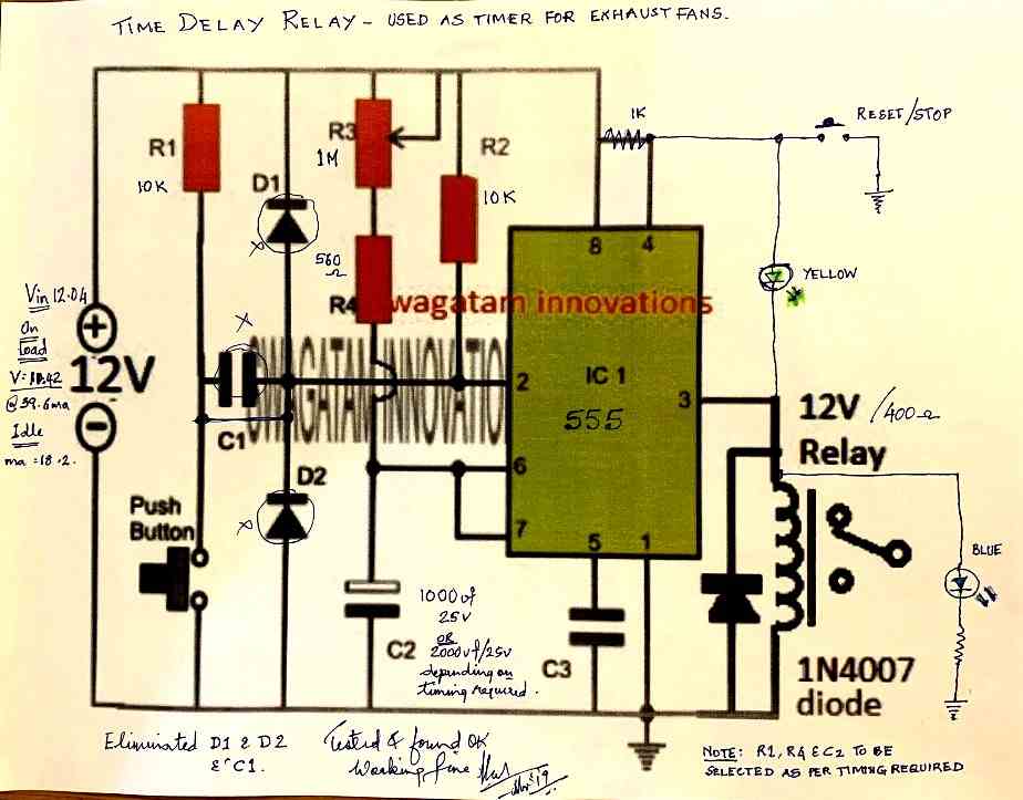 The prototype images of the above timer unit can be witnessed as shown below (built and tested by Mr.
Vee):
The prototype images of the above timer unit can be witnessed as shown below (built and tested by Mr.
Vee):
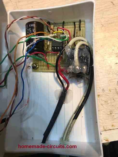
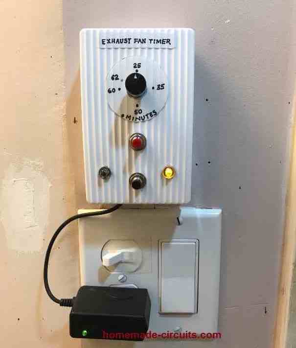
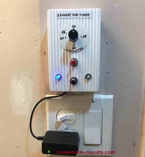
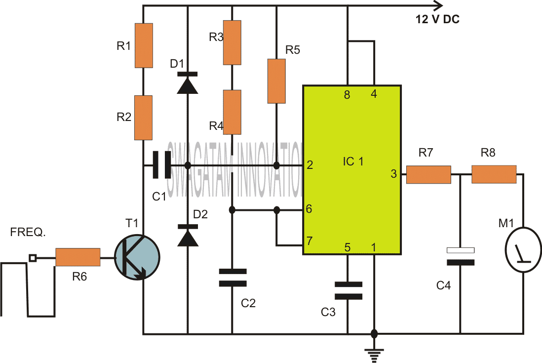
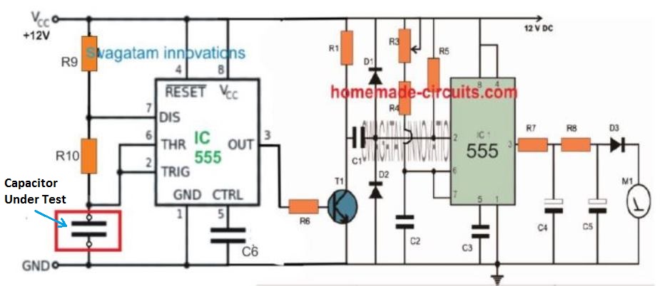 Therefore, the net frequency value now shown at the output will correspond to the value of the capacitor connected across the above discussed points.
That means now we have a two in one circuit which can measure capacitance as well as frequency, using just a couple of ICs and some casual electronic parts.
With little modifications the circuit can be easily used as a tachometer or as RPM counter equipment.
Therefore, the net frequency value now shown at the output will correspond to the value of the capacitor connected across the above discussed points.
That means now we have a two in one circuit which can measure capacitance as well as frequency, using just a couple of ICs and some casual electronic parts.
With little modifications the circuit can be easily used as a tachometer or as RPM counter equipment.
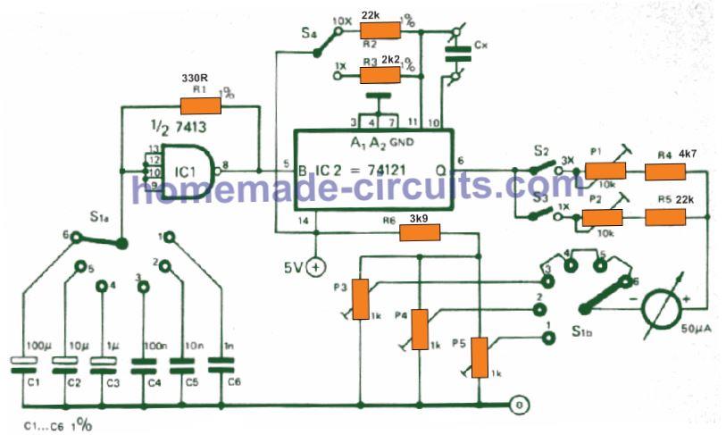 This stage activates the IC 74121 (a monostable multivibrator) so that it generates an asymmetric square wave with a recurring frequency whse value is decided by the parts R1 and C1 to C6 and with a duty cycle as decided by R2 (or R3) and Cx.
The typical value of this square -wave voltage changes linearly as the duty cycle is changed, which in turn is modifies linearly based on the value of Cs, the value of R2/R3 (s10/x I) and the frequency (established by the S1 switch position).
The final range selector switches S3j..-xl) and 52 (x3) basically insert a resistor in series with the meter.
The configuration around the pins 10 and pin 11 of the IC 74121, and for the Cx must be as short and stiff as is feasible, to ensure that stray capacitance here is minimal and without fluctuations.
P5 and P4 are employed for independent zero calibration for low capacitance ranges.
For all higher ranges, calibration done by oreset P3 is just sufficient.
F.s.d.
calibration is rather straightforward.
Do not initially solder C6 in circuit rather attach it over the terminals marked Cx for the unknown capacitor.
Put S1 in position 3, S4 in position x1 and S2 closed (s3); this gets set up for the ranges of 1500 pF f.s.d.
Now, C6 becomes ready to be applied as a calibration bench mark value.
Next, pot P1 is tweaked until the meter deciphers 2/3 of f.s.d.
Then, S4 could be moved to position ' x 10', S2 held open and S3 is closed (x1 ); this compares to 5000 pF f.s.d., while working with C6 as the unknown capacitor.
The result for these complete set up should provide 1/5 of fs.d.
On the other hand you can procure an assortment of accurately known capacitors and use these across the Cx points and then adjust the various pots for fixing the calibrations on the meter dial appropriately.
This stage activates the IC 74121 (a monostable multivibrator) so that it generates an asymmetric square wave with a recurring frequency whse value is decided by the parts R1 and C1 to C6 and with a duty cycle as decided by R2 (or R3) and Cx.
The typical value of this square -wave voltage changes linearly as the duty cycle is changed, which in turn is modifies linearly based on the value of Cs, the value of R2/R3 (s10/x I) and the frequency (established by the S1 switch position).
The final range selector switches S3j..-xl) and 52 (x3) basically insert a resistor in series with the meter.
The configuration around the pins 10 and pin 11 of the IC 74121, and for the Cx must be as short and stiff as is feasible, to ensure that stray capacitance here is minimal and without fluctuations.
P5 and P4 are employed for independent zero calibration for low capacitance ranges.
For all higher ranges, calibration done by oreset P3 is just sufficient.
F.s.d.
calibration is rather straightforward.
Do not initially solder C6 in circuit rather attach it over the terminals marked Cx for the unknown capacitor.
Put S1 in position 3, S4 in position x1 and S2 closed (s3); this gets set up for the ranges of 1500 pF f.s.d.
Now, C6 becomes ready to be applied as a calibration bench mark value.
Next, pot P1 is tweaked until the meter deciphers 2/3 of f.s.d.
Then, S4 could be moved to position ' x 10', S2 held open and S3 is closed (x1 ); this compares to 5000 pF f.s.d., while working with C6 as the unknown capacitor.
The result for these complete set up should provide 1/5 of fs.d.
On the other hand you can procure an assortment of accurately known capacitors and use these across the Cx points and then adjust the various pots for fixing the calibrations on the meter dial appropriately.
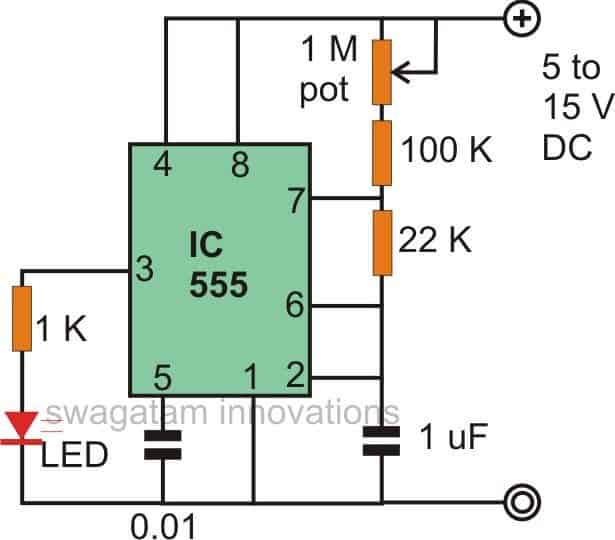 The first figure shows the basic configuration associated with 555 ICs, here it is connected as an astable multivibrator.
The resistors and the capacitor 1 uF can be experimented with to get different rates of blinking over the connected LED.
The LEDs can also be used with oter colors.
The 1 K resistor can be replaced with lower values for increasing the intensity of the LED, however it should not be redced below 330 Ohms.
Alternatively the 1 M resistor can be interchanged with a pot for attributing the circuit with variable blinking rate feature.
The first figure shows the basic configuration associated with 555 ICs, here it is connected as an astable multivibrator.
The resistors and the capacitor 1 uF can be experimented with to get different rates of blinking over the connected LED.
The LEDs can also be used with oter colors.
The 1 K resistor can be replaced with lower values for increasing the intensity of the LED, however it should not be redced below 330 Ohms.
Alternatively the 1 M resistor can be interchanged with a pot for attributing the circuit with variable blinking rate feature.
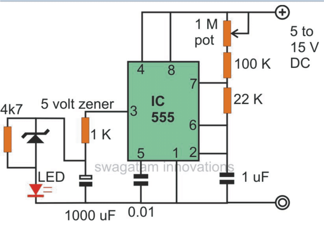
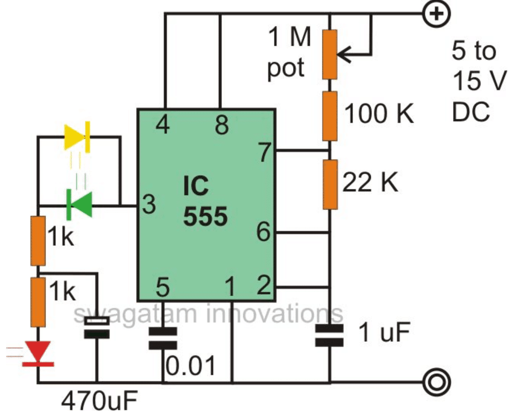 The above effect can be simplified by the circuit shown below.
Here, the LED which is connected to the 1 K resistor blinks at the fixed blinking rate, but the next LED which is connected to the ground switches rapidly at some other defined rate.
The above effect can be simplified by the circuit shown below.
Here, the LED which is connected to the 1 K resistor blinks at the fixed blinking rate, but the next LED which is connected to the ground switches rapidly at some other defined rate.
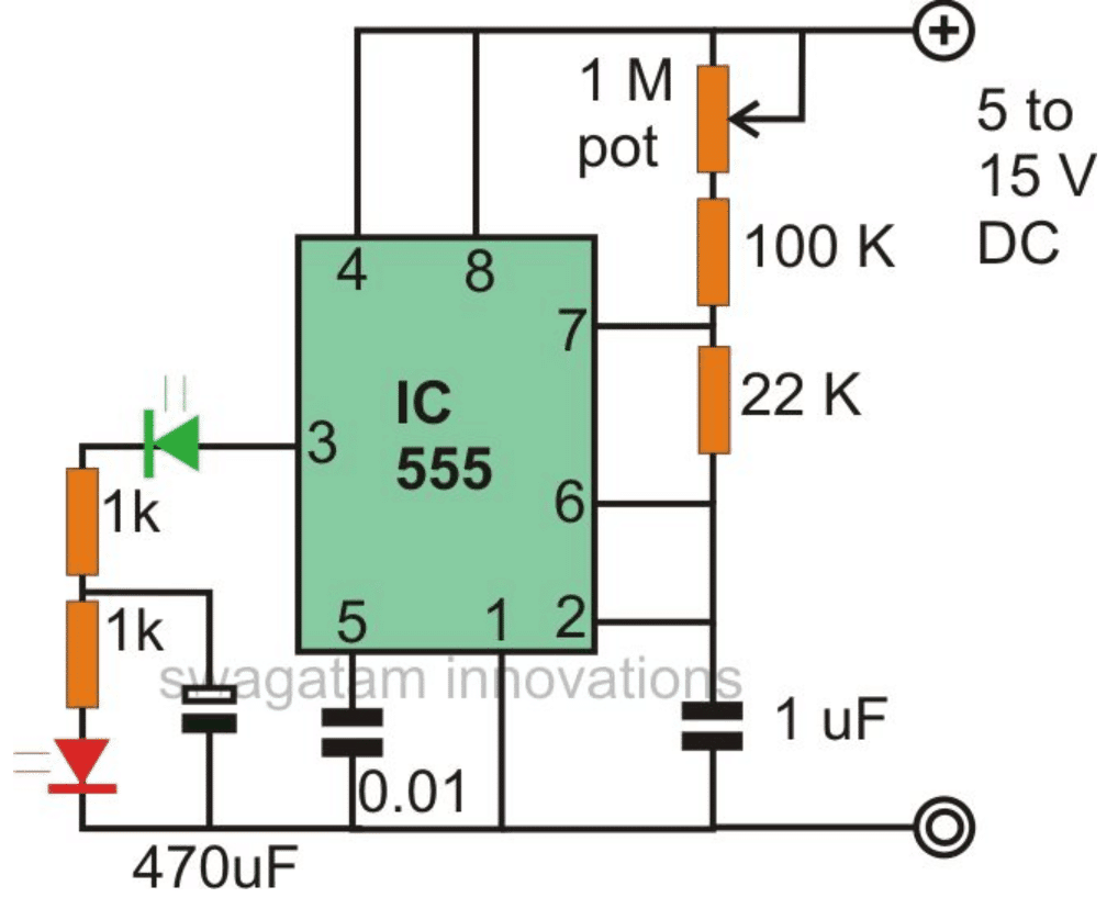
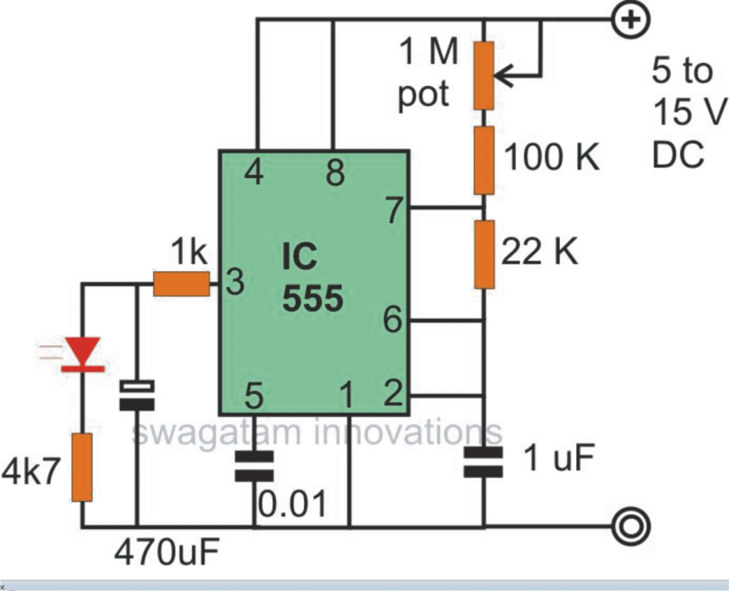
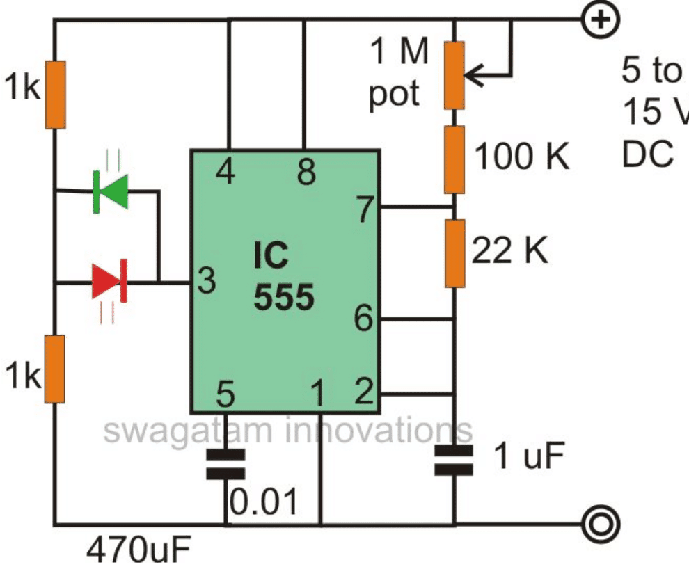 The above circuit can be further modified as shown below by complely disarranging the network with the shown type.
Here the LEDs though blink alternately, the intensity may fluctuate from dim to bright over the LEDs.
The above circuit can be further modified as shown below by complely disarranging the network with the shown type.
Here the LEDs though blink alternately, the intensity may fluctuate from dim to bright over the LEDs.
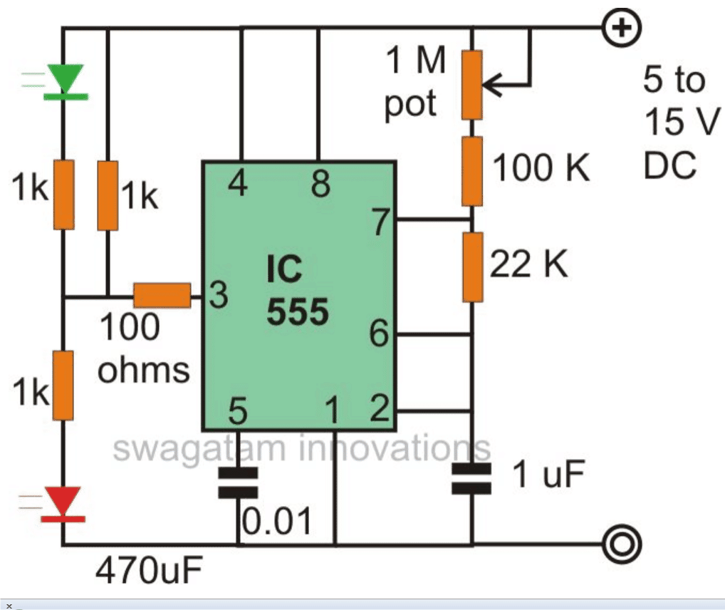
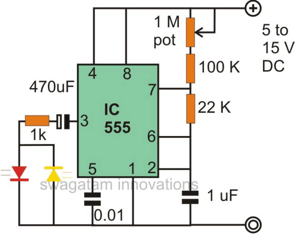
 The circuit working is very basic.
The zener diode ZD is gets the supply from the positive line through resistor R1. A fixed reference voltage of 12V is produced over the zener diode, which is supplied to an adjustable voltage divider RV1.
The divider output is completely adjustable from 0V to 12V, which is applied to the non-inverting input of the op amp 741.
The op amp is configured like an unity gain voltage follower, with transistor Q1 rigged in the form of an emitter follower current amplifier stage, connected in series with its output.
Therefore, the output voltage from the power supply circuit tracks and follows the voltage established at the input of the op amp input by means of RV1, which is totally adjustable from 0V to 12V.
Remember that this specific 741 power supply circuit employs an 18V positive supply and a 9V negative supply.
Additionally, the output voltage range of the present circuit could be made higher through the use of higher rated zener diode and through the supply of higher rated unregulated input supply voltages.
The specifications of the current could be likewise made higher by incorporating a couple of more power transistors in place of the existing transistor Q1.
The circuit working is very basic.
The zener diode ZD is gets the supply from the positive line through resistor R1. A fixed reference voltage of 12V is produced over the zener diode, which is supplied to an adjustable voltage divider RV1.
The divider output is completely adjustable from 0V to 12V, which is applied to the non-inverting input of the op amp 741.
The op amp is configured like an unity gain voltage follower, with transistor Q1 rigged in the form of an emitter follower current amplifier stage, connected in series with its output.
Therefore, the output voltage from the power supply circuit tracks and follows the voltage established at the input of the op amp input by means of RV1, which is totally adjustable from 0V to 12V.
Remember that this specific 741 power supply circuit employs an 18V positive supply and a 9V negative supply.
Additionally, the output voltage range of the present circuit could be made higher through the use of higher rated zener diode and through the supply of higher rated unregulated input supply voltages.
The specifications of the current could be likewise made higher by incorporating a couple of more power transistors in place of the existing transistor Q1.
 In this configuration, the supply to the 741 op amp is stabilized at 33V by using the zener diode ZD1. Another extremely temperature stabilized, constant reference voltage of 3V is achieved through the zener diode ZD2, and this applied to the non inverting input of the IC 741 .
The transistors Q1, Q2 are connected with the output of the op amp, and are configured like a variable gain non inverting d.c.
amplifier.
This set up has a gain which can be varied from unity to x10, by means of RV1.
This provides an output voltage that is completely adjustable from 3V to 30V through the pot RV1. The output voltage generated by this IC 741 power supply features a fully stabilized voltage using a negative feedback loop.
In this configuration, the supply to the 741 op amp is stabilized at 33V by using the zener diode ZD1. Another extremely temperature stabilized, constant reference voltage of 3V is achieved through the zener diode ZD2, and this applied to the non inverting input of the IC 741 .
The transistors Q1, Q2 are connected with the output of the op amp, and are configured like a variable gain non inverting d.c.
amplifier.
This set up has a gain which can be varied from unity to x10, by means of RV1.
This provides an output voltage that is completely adjustable from 3V to 30V through the pot RV1. The output voltage generated by this IC 741 power supply features a fully stabilized voltage using a negative feedback loop.
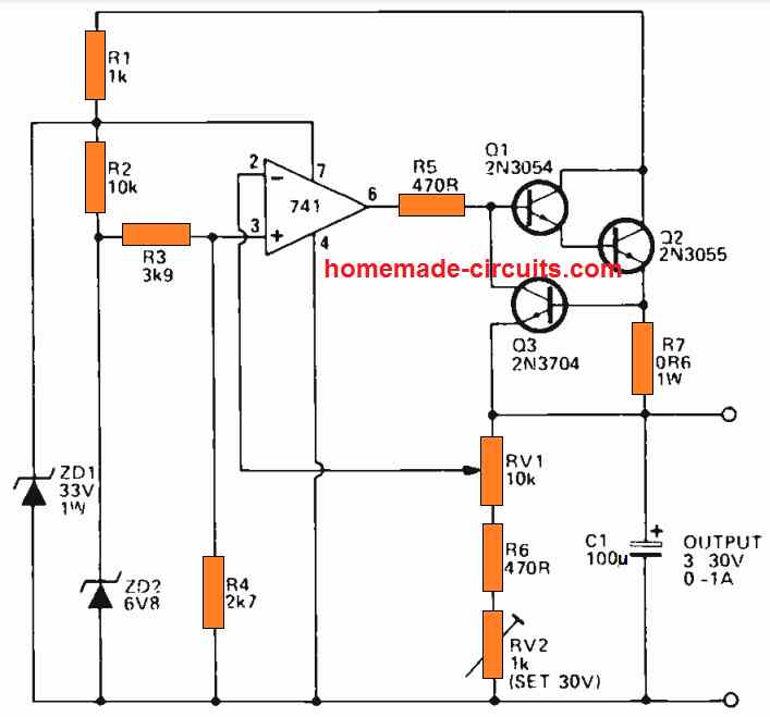 The transistor Q3 which is the shut-down transistor is powered through this resistor R7 and is configured such that its base-collector junction has the ability to short the Q1, Q2 base-emitter junction of the output transistor stage.
Typically, Q3 stays deactivated, and it does not effect the functioning of the circuit.
However, as soon as the output currents of the power supply reaches beyond the 1A mark, a voltage difference of over 600 mV is produced across R7, it instantly begins biasing the transistor Q3 base, switching it ON.
As a result Q3 is forced to shunt the base-emitter junction of the Q1-Q2 output stage to ground.
Consequently, the action causes an instant reduction of the output current, generating a large negative feedback across the connected loop.
This action causes an automatic limiting of the output current within the 1A range.
The same procedure is implemented during a short-circuit conditions also, providing a full short circuit and over load protection to this IC 741 power supply circuit.
The transistor Q3 which is the shut-down transistor is powered through this resistor R7 and is configured such that its base-collector junction has the ability to short the Q1, Q2 base-emitter junction of the output transistor stage.
Typically, Q3 stays deactivated, and it does not effect the functioning of the circuit.
However, as soon as the output currents of the power supply reaches beyond the 1A mark, a voltage difference of over 600 mV is produced across R7, it instantly begins biasing the transistor Q3 base, switching it ON.
As a result Q3 is forced to shunt the base-emitter junction of the Q1-Q2 output stage to ground.
Consequently, the action causes an instant reduction of the output current, generating a large negative feedback across the connected loop.
This action causes an automatic limiting of the output current within the 1A range.
The same procedure is implemented during a short-circuit conditions also, providing a full short circuit and over load protection to this IC 741 power supply circuit.
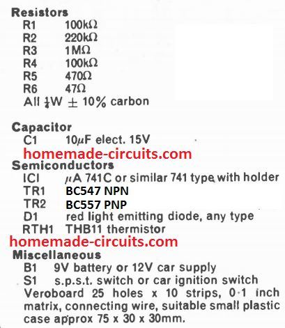 The entire circuit of the "frost" alarm is revealed in the above figure.
It is driven by the voltage from the 12V car battery.
Alternatively, for other applications a 9V battery might be enough to run the circuit.
The circuit basically is made up of a couple of elements broken down by the dotted line.
On the left of this line shows the temperature sensitive Wheatstone bridge, whose output is detected by the op amp operating like a differential amplifier.
Towards the right of the dotted line exists a two-transistor oscillator that oscillates the LED as soon as the thermistor extends to the preset temperature.
The Wheatstone bridge includes resistors R1 and R2 which fixes the voltage on the inverting terminal of the op amp at around 8V with reference to the ground line (for a 12V battery).
The preset VR1 and the thermistor RTh2create the second arms of the bridge.
This is because the thermistor is an NTC specification, you will find as the temperature comes down its resistance increases, causing the voltage at pin 3 to rise proportionately.
As this voltage just crosses the reference level of pin 2, the output of the op amp changes status and flips from around zero to some volts positive.
The temperature where the output moves dramatically positive could be determined by fine tuning of the preset VR1. The quick increase in voltage at the output of the op amp turns oscillator circuit shown at the right side of the dotted line.
Resistor R3 uses this voltage to switch the base of transistor TR1.
The capacitor C1 helps with the positive feedback essential to hold the low-frequency amplitudes.
The pnp transistor TR2 powers LED in its collector terminal along with a calculated series resistor R5 which limits the current entering the LED at under the maximum rating.
The LED flashing frequency is established to a certain extent by its own resistance although it is adjustable to the desired level by choosing an appropriate magnitude for Cl.
Transistors TRI and TR2 needs to be a complementary match for the circuit to function optimally.
The entire circuit of the "frost" alarm is revealed in the above figure.
It is driven by the voltage from the 12V car battery.
Alternatively, for other applications a 9V battery might be enough to run the circuit.
The circuit basically is made up of a couple of elements broken down by the dotted line.
On the left of this line shows the temperature sensitive Wheatstone bridge, whose output is detected by the op amp operating like a differential amplifier.
Towards the right of the dotted line exists a two-transistor oscillator that oscillates the LED as soon as the thermistor extends to the preset temperature.
The Wheatstone bridge includes resistors R1 and R2 which fixes the voltage on the inverting terminal of the op amp at around 8V with reference to the ground line (for a 12V battery).
The preset VR1 and the thermistor RTh2create the second arms of the bridge.
This is because the thermistor is an NTC specification, you will find as the temperature comes down its resistance increases, causing the voltage at pin 3 to rise proportionately.
As this voltage just crosses the reference level of pin 2, the output of the op amp changes status and flips from around zero to some volts positive.
The temperature where the output moves dramatically positive could be determined by fine tuning of the preset VR1. The quick increase in voltage at the output of the op amp turns oscillator circuit shown at the right side of the dotted line.
Resistor R3 uses this voltage to switch the base of transistor TR1.
The capacitor C1 helps with the positive feedback essential to hold the low-frequency amplitudes.
The pnp transistor TR2 powers LED in its collector terminal along with a calculated series resistor R5 which limits the current entering the LED at under the maximum rating.
The LED flashing frequency is established to a certain extent by its own resistance although it is adjustable to the desired level by choosing an appropriate magnitude for Cl.
Transistors TRI and TR2 needs to be a complementary match for the circuit to function optimally.
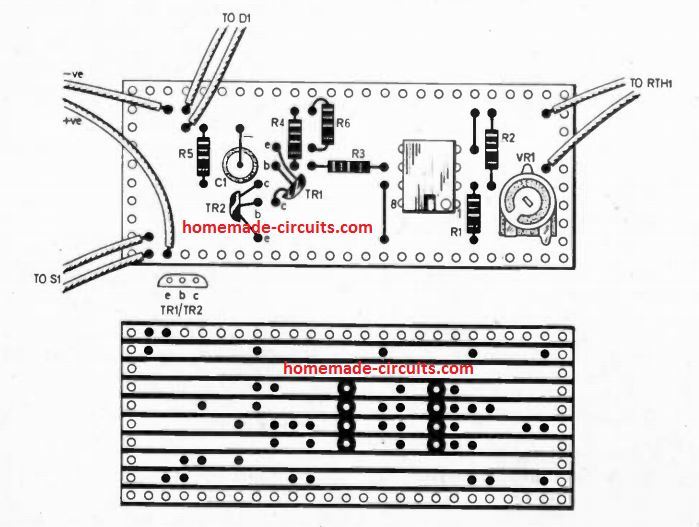 The thermistor should be positioned far away from any possible heat source or from the engine.
It should be near to the floor of the car for easier sensing of the temperatures of the frosty icy patches on roads just a feet below.
The thermistor has to be shielded from possible water splashes or rain, because chilling effect due to the water evaporating may cause sudden drop in it temperature below the actual surrounding temperature, leading to false alarms.
An effective placement of the thermistor is at the rear of the front bumper however the an even a better place could be identified depending on the type of car.
Once the correct placement for the thermistor is found, you need to determine the wire distance needed between the thermistor and the control circuit.
Exercise caution while soldering the extension wire to the thermistor owing to the fact that the soldered joints must be protected using sleeving to shield against water contact.
Sleeving with heat-shrinkable property may serve as the best option.
The thermistor must be cemented into the finish of a short plastic tube to ensure that while air is allowed to flow around it, it stays aloof from possible water splashes.
Just about any tiny plastic box may be used to enclose the circuit and also to position it safely right somewhere behind the car dashboard.
Three sets of output wires ought to terminate the box via a grommet: a couple of wires will go to the battery, 2 to the thermistor, and 2 to the LED.
Pick a location within the dash which may be most appropriate for visualizing the LED flashing.
Drill down a hole to pass the LED in a way that it enables an easy push through a plastic grommet.
The LED should be joined accurately to the circuit in order that it TR2 is able to switching it on correctly with a forward bias.
You can easily identify the LED anode pin through a multimeter set to its ohms range.
Before the final installation of the circuit inside the car, the results must be confirmed with an actual ice temperature testing.
The thermistor should be positioned far away from any possible heat source or from the engine.
It should be near to the floor of the car for easier sensing of the temperatures of the frosty icy patches on roads just a feet below.
The thermistor has to be shielded from possible water splashes or rain, because chilling effect due to the water evaporating may cause sudden drop in it temperature below the actual surrounding temperature, leading to false alarms.
An effective placement of the thermistor is at the rear of the front bumper however the an even a better place could be identified depending on the type of car.
Once the correct placement for the thermistor is found, you need to determine the wire distance needed between the thermistor and the control circuit.
Exercise caution while soldering the extension wire to the thermistor owing to the fact that the soldered joints must be protected using sleeving to shield against water contact.
Sleeving with heat-shrinkable property may serve as the best option.
The thermistor must be cemented into the finish of a short plastic tube to ensure that while air is allowed to flow around it, it stays aloof from possible water splashes.
Just about any tiny plastic box may be used to enclose the circuit and also to position it safely right somewhere behind the car dashboard.
Three sets of output wires ought to terminate the box via a grommet: a couple of wires will go to the battery, 2 to the thermistor, and 2 to the LED.
Pick a location within the dash which may be most appropriate for visualizing the LED flashing.
Drill down a hole to pass the LED in a way that it enables an easy push through a plastic grommet.
The LED should be joined accurately to the circuit in order that it TR2 is able to switching it on correctly with a forward bias.
You can easily identify the LED anode pin through a multimeter set to its ohms range.
Before the final installation of the circuit inside the car, the results must be confirmed with an actual ice temperature testing.
 Here, the output responds with a "high" digital signal, whenever the voltage at the non-inverting (+) input is higher than the inverting (-) input.
Oppositely, the output into a turns low digital signal, whenever the noninverting input voltage is lower than the inverting input voltage.
Here, the output responds with a "high" digital signal, whenever the voltage at the non-inverting (+) input is higher than the inverting (-) input.
Oppositely, the output into a turns low digital signal, whenever the noninverting input voltage is lower than the inverting input voltage.
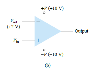 Referring to the above figure above, we can see a standard connection of a comparator circuit having one input (the inverting input in this example) configured with a reference voltage, and the other input pin which is the noninverting input connected to an input signal voltage.
During the time Vin is held at lower voltage than the reference voltage of +2 V, the output stays low at around -10 V.
If Vin is increased just above +2 V, the output instantly changes state, and turns high to around +10 V.
This change of state at the output from -10 V to +10 V indicates that the Vin has become higher than the reference +2 V.
The main component inside any comparator is an op amp circuit, which set at a very high voltage gain.
To study the working of a comparator accurately we can take the example of the IC 741, as shown below:
Referring to the above figure above, we can see a standard connection of a comparator circuit having one input (the inverting input in this example) configured with a reference voltage, and the other input pin which is the noninverting input connected to an input signal voltage.
During the time Vin is held at lower voltage than the reference voltage of +2 V, the output stays low at around -10 V.
If Vin is increased just above +2 V, the output instantly changes state, and turns high to around +10 V.
This change of state at the output from -10 V to +10 V indicates that the Vin has become higher than the reference +2 V.
The main component inside any comparator is an op amp circuit, which set at a very high voltage gain.
To study the working of a comparator accurately we can take the example of the IC 741, as shown below:
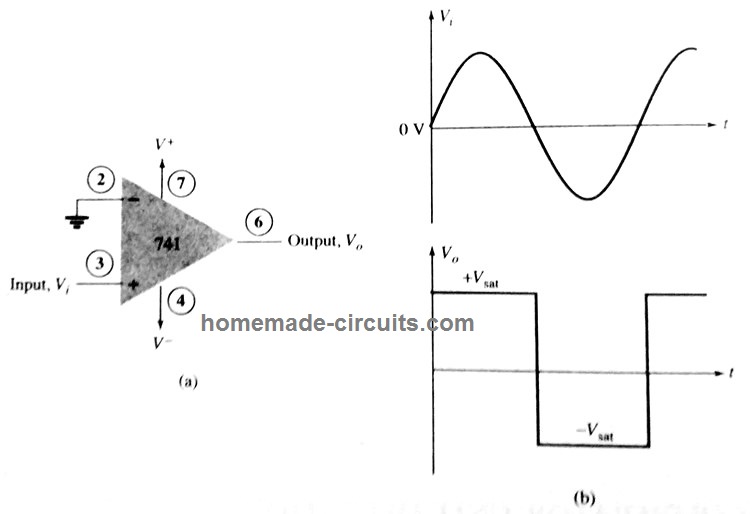 Here we can see the inverting input pin2 (-) is referenced to ground, or a 0 V level.
A sinusoidal signal is applied on pin3 which is the noninverting input of the op amp.
This alternately varying sinusoidal signal causes the output to switch between high and low output states, as indicated on the right side of the image.
When the input Vin moves even a millivolt over the 0 V reference, the difference is amplified by the internal high gain op amp of the IC, causing the output to go high at the output positive saturation level.
This condition is sustained for so long as Vin signal stays above the 0 V reference.
Now, as soon as the signal level drops a shade below the 0 V reference, the output is driven to its lower level of saturation.
Again, this condition is maintained as long as the Vin input signal stays below the 0 V reference level.
The above explanation and the waveform presented in the image clearly indicates the digital response of the output for a linearly varying input signal.
For normal applications, the reference level doesn't have to be at 0 V, rather can be any positive level as per the requirement.
And, in case required the reference can be also connected either to the positive or the negative supply lines, while the input signal is applied at the other input pin.
Here we can see the inverting input pin2 (-) is referenced to ground, or a 0 V level.
A sinusoidal signal is applied on pin3 which is the noninverting input of the op amp.
This alternately varying sinusoidal signal causes the output to switch between high and low output states, as indicated on the right side of the image.
When the input Vin moves even a millivolt over the 0 V reference, the difference is amplified by the internal high gain op amp of the IC, causing the output to go high at the output positive saturation level.
This condition is sustained for so long as Vin signal stays above the 0 V reference.
Now, as soon as the signal level drops a shade below the 0 V reference, the output is driven to its lower level of saturation.
Again, this condition is maintained as long as the Vin input signal stays below the 0 V reference level.
The above explanation and the waveform presented in the image clearly indicates the digital response of the output for a linearly varying input signal.
For normal applications, the reference level doesn't have to be at 0 V, rather can be any positive level as per the requirement.
And, in case required the reference can be also connected either to the positive or the negative supply lines, while the input signal is applied at the other input pin.
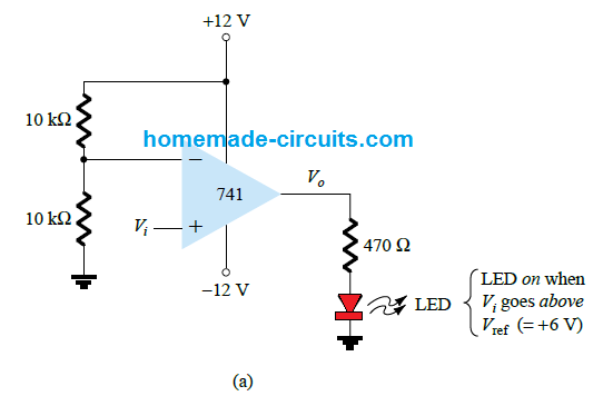 In the figure we can see an op amp circuit working with a positive reference set at its inverting input pin (-).
The output is attached with an LED.
Using the voltage divider network formula, we can calculate the refernce voltage value on the (-) input pin of the IC.
Vref = 10 k / 10 k + 10 k x +12 V = +6 V
Since this reference is associated with (-) pin of the IC, if the voltage Vin at the (+) input goes higher than this reference or becomes more positive than the reference, will force the output Vo to switch to its positive saturation level.
This will cause the LED to illuminate, indicating that Vin has become more positive than the reference level of +6 V.
Oppositely if the noninverting input (+) is configured as the reference pin and Vin applied to the inverting input (-) pin, the output will go low as soon as the Vin input goes below reference value, and vice versa.
This will instantly cause the LED to shut off.
Therefore, the LED can be made to switch ON or OFF for a given input signal, by appropriately wiring the inputs pin with the reference level and the input signal.
In the figure we can see an op amp circuit working with a positive reference set at its inverting input pin (-).
The output is attached with an LED.
Using the voltage divider network formula, we can calculate the refernce voltage value on the (-) input pin of the IC.
Vref = 10 k / 10 k + 10 k x +12 V = +6 V
Since this reference is associated with (-) pin of the IC, if the voltage Vin at the (+) input goes higher than this reference or becomes more positive than the reference, will force the output Vo to switch to its positive saturation level.
This will cause the LED to illuminate, indicating that Vin has become more positive than the reference level of +6 V.
Oppositely if the noninverting input (+) is configured as the reference pin and Vin applied to the inverting input (-) pin, the output will go low as soon as the Vin input goes below reference value, and vice versa.
This will instantly cause the LED to shut off.
Therefore, the LED can be made to switch ON or OFF for a given input signal, by appropriately wiring the inputs pin with the reference level and the input signal.
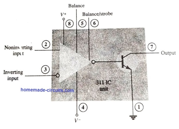 The figure above shows the internal layout and the pinout details of the comparator IC 311. The IC is designed to operate from a dual power supply also, in the range of +15 V and -15 V, which is a standard compatible level for all modern digital ICs.
The output stage inside the IC has a bipolar transistor, having floating collector and emitter terminals.
This means that the output from this transistor can be configured can be configured in two different ways:
By adding a pull-up resistor with the collector pin7 and grounding the emitter pin1, and subsequently using the collector as the output.
By joining the collector with the positive line and using the emitter as the output.
The transistor output can be also used for driving a relay or a small load such as a lamp directly without any external buffer stage.
The IC also features a balance and a strobe input which can be gated with the output.
We'll discuss a few useful applications of this IC in the following sections:
The figure above shows the internal layout and the pinout details of the comparator IC 311. The IC is designed to operate from a dual power supply also, in the range of +15 V and -15 V, which is a standard compatible level for all modern digital ICs.
The output stage inside the IC has a bipolar transistor, having floating collector and emitter terminals.
This means that the output from this transistor can be configured can be configured in two different ways:
By adding a pull-up resistor with the collector pin7 and grounding the emitter pin1, and subsequently using the collector as the output.
By joining the collector with the positive line and using the emitter as the output.
The transistor output can be also used for driving a relay or a small load such as a lamp directly without any external buffer stage.
The IC also features a balance and a strobe input which can be gated with the output.
We'll discuss a few useful applications of this IC in the following sections:
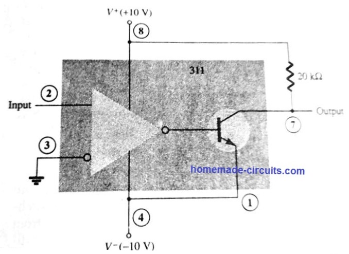 The figure above shows how the IC 311 can be configured like a zero-crossing detector comparator to sense the input voltage, whenever it crosses the zero line.
The inverting input (-) of the 311 can be seen joined with the ground.
During the period the input signal is at the positive level, the output transistor remains switched ON, which creates a low (-10 in this example) at the output (transistor collector).
As soon as the input signal goes negative or below 0 V, the transistor is turned OFF.
This creates a positive +10V at the collector output of the IC.
This allows us to know when the input signal is above the zero level and when it has dropped below the zero level.
The next figure below shows how IC 311 comparator can be used for making a strobed circuit.
In this comparator circuit example, the output pin7 will turn high when pin3 voltage level rises above pin2 reference.
But this can happen only while pin6 strobe input pin is low or at 0 V.
The figure above shows how the IC 311 can be configured like a zero-crossing detector comparator to sense the input voltage, whenever it crosses the zero line.
The inverting input (-) of the 311 can be seen joined with the ground.
During the period the input signal is at the positive level, the output transistor remains switched ON, which creates a low (-10 in this example) at the output (transistor collector).
As soon as the input signal goes negative or below 0 V, the transistor is turned OFF.
This creates a positive +10V at the collector output of the IC.
This allows us to know when the input signal is above the zero level and when it has dropped below the zero level.
The next figure below shows how IC 311 comparator can be used for making a strobed circuit.
In this comparator circuit example, the output pin7 will turn high when pin3 voltage level rises above pin2 reference.
But this can happen only while pin6 strobe input pin is low or at 0 V.
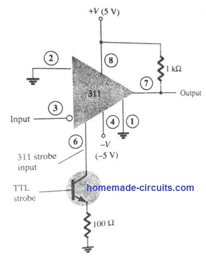 When a high TTL strobe is applied at the base of the transistor, pin6 becomes low, causing the IC output transistor to switch off, and thereby enabling pin7 to go high.
The output continues to be high as long as the TTL input is held high, regardless of the input signal condition at pin3.
However, if the TTL signal is applied in strobed form, then the output responds to the input signal at pin3. Put simply, the output remains locked at high, unless pin6 is strobed.
When a high TTL strobe is applied at the base of the transistor, pin6 becomes low, causing the IC output transistor to switch off, and thereby enabling pin7 to go high.
The output continues to be high as long as the TTL input is held high, regardless of the input signal condition at pin3.
However, if the TTL signal is applied in strobed form, then the output responds to the input signal at pin3. Put simply, the output remains locked at high, unless pin6 is strobed.
 Here, when the voltage level at input pin2 drops below 0 V, pin3 gets more positive than pin2. This causes the collector of the internal transistor to switch OFF, which switches ON the relay.
The contacts of the relay could be wired with a heavier load for executing a desired switching action.
As long as the (+) input at pin2 stays below 0 V, the relay remains switched ON.
Conversely, when a positive signal is available on pin2, the relay will remain switched OFF.
Here, when the voltage level at input pin2 drops below 0 V, pin3 gets more positive than pin2. This causes the collector of the internal transistor to switch OFF, which switches ON the relay.
The contacts of the relay could be wired with a heavier load for executing a desired switching action.
As long as the (+) input at pin2 stays below 0 V, the relay remains switched ON.
Conversely, when a positive signal is available on pin2, the relay will remain switched OFF.
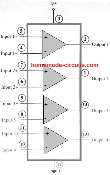 Just like any other comparator, each comparator block has a couple of inputs, and one output.
When the IC is powered by applying voltage across the Vcc, and ground supply pins, it powers all the comparators together.
So even if a single comparator is used, all the other 3 would be consuming some power.
All the comparator have exactly identical characteristics, therefore we can analyze any one of these to learn the basic comparator function.
Just like any other comparator, each comparator block has a couple of inputs, and one output.
When the IC is powered by applying voltage across the Vcc, and ground supply pins, it powers all the comparators together.
So even if a single comparator is used, all the other 3 would be consuming some power.
All the comparator have exactly identical characteristics, therefore we can analyze any one of these to learn the basic comparator function.
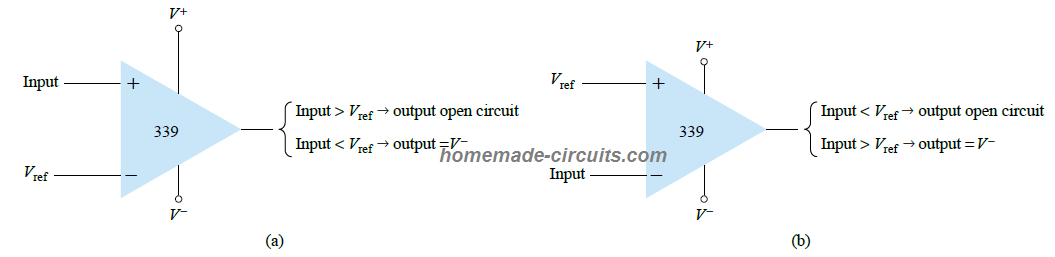 When a positive differential input is applied across the input terminals, meaning when the difference between the applied signals is positive, it turns the output transistor OFF.
This causes the output to show an open circuit, or a floating open.
When the differential input is negative, meaning when the difference between the applied signals at the input pins is negative, it turns ON the output transistor of the comparator, which causes the output pin of the comparator to turn negative, or at V- potential.
Referring to the figure above, we can understand that when the non-inverting (+) input of the IC is used as the reference pin, a voltage lower than this reference at the inverting input pin (-) will result in the output of the comparator to become open.
On the other hand, if the (-) is used as the reference pin, a voltage level at the (+) input higher than the reference will cause the output to turn negative or at V-
In order to learn how the IC 339 works like a comparator, the following example shows the IC as a zero crossing detector.
When a positive differential input is applied across the input terminals, meaning when the difference between the applied signals is positive, it turns the output transistor OFF.
This causes the output to show an open circuit, or a floating open.
When the differential input is negative, meaning when the difference between the applied signals at the input pins is negative, it turns ON the output transistor of the comparator, which causes the output pin of the comparator to turn negative, or at V- potential.
Referring to the figure above, we can understand that when the non-inverting (+) input of the IC is used as the reference pin, a voltage lower than this reference at the inverting input pin (-) will result in the output of the comparator to become open.
On the other hand, if the (-) is used as the reference pin, a voltage level at the (+) input higher than the reference will cause the output to turn negative or at V-
In order to learn how the IC 339 works like a comparator, the following example shows the IC as a zero crossing detector.
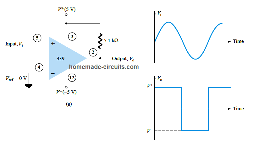 The moment the input signal rises above 0 V, the output is turned high at V+ level.
The output is turned OFF at V- only while the input is held below 0 V.
As explained previously, the reference level does not need to be 0 V, it can be changed to any other desired level.
Additionally, you can also use the other input pin (+) as the reference pin, and the (-) input pin as the signal input pin for accepting the varying input signal.
The moment the input signal rises above 0 V, the output is turned high at V+ level.
The output is turned OFF at V- only while the input is held below 0 V.
As explained previously, the reference level does not need to be 0 V, it can be changed to any other desired level.
Additionally, you can also use the other input pin (+) as the reference pin, and the (-) input pin as the signal input pin for accepting the varying input signal.
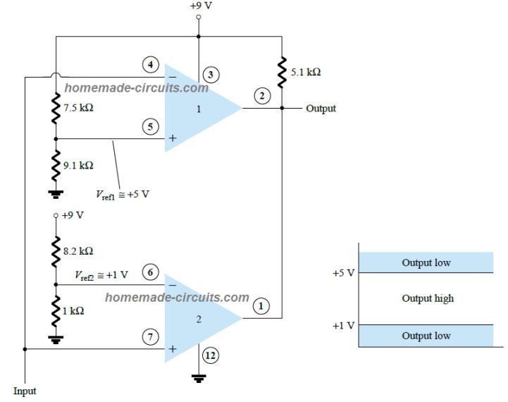 The output of the respective comparators go low whenever the input signal crosses either the lower set threshold or the upper set threshold, thus enabling the user to know when the signal is out of the set window level.
A window comparator can be used for useful applications such as high low voltage protector circuit, and solar tracker circuit etc.
The output of the respective comparators go low whenever the input signal crosses either the lower set threshold or the upper set threshold, thus enabling the user to know when the signal is out of the set window level.
A window comparator can be used for useful applications such as high low voltage protector circuit, and solar tracker circuit etc.
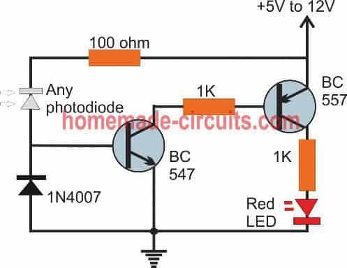
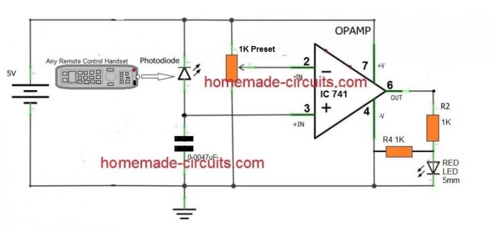 Video Clip
The remote control tester above using an opamp also looks pretty straightforward.
An ordinary opamp 741 is employed here for the detection.
It is configured as a comparator.
Its inverting input pin#2 is used as a reference level, and is set by fixing the connected preset.
The photodiode can be seen connected across the the non-inverting pin#3 and the positive line.
The preset is adjusted such that in normal condition when no signal is being received by the photodiode, the LED at pin#6 stays just shut off.
This is actually very easy, just switch ON power and begin adjusting the preset to-and-fro, and set it at a point where the LED just remains shut-off.
Next, point a TV remote control handset towards the photodiode, press any of the buttons of the remote control, you will instantly find the LED blinking in response to the remote control's coded IR signals.
Video Clip
The remote control tester above using an opamp also looks pretty straightforward.
An ordinary opamp 741 is employed here for the detection.
It is configured as a comparator.
Its inverting input pin#2 is used as a reference level, and is set by fixing the connected preset.
The photodiode can be seen connected across the the non-inverting pin#3 and the positive line.
The preset is adjusted such that in normal condition when no signal is being received by the photodiode, the LED at pin#6 stays just shut off.
This is actually very easy, just switch ON power and begin adjusting the preset to-and-fro, and set it at a point where the LED just remains shut-off.
Next, point a TV remote control handset towards the photodiode, press any of the buttons of the remote control, you will instantly find the LED blinking in response to the remote control's coded IR signals.
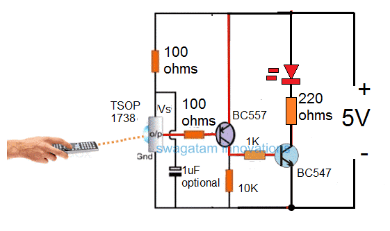 Again the remote tester design using a TSOP1738 appears extremely straightforward.
The connection arrangement of the TSOP IC is in its standard form, rest of the circuit is as simple as it can be.
Just a couple of transistors are enough to get the circuit working in the most versatile way.
The great feature of this circuit is its immunity to noise and ambient light, not forgetting the sensitivity and range too.
The detection range is actually awesome, you can point the remote handset to an opposite wall and still get the LED to respond efficiently from the reflected IR rays.
The aim of the above explained remote tester circuits is to show how a simple IR circuit can beused for activating an LED in response to IR rays from any ordinary IR remote control system.
The LED can be easily replaced with a relay for accomplishing more complex jobs as per a given application requirement, or as per user preference.
Have questions? You can put them forth as comments below, all your queries will be addressed ASAP.
Again the remote tester design using a TSOP1738 appears extremely straightforward.
The connection arrangement of the TSOP IC is in its standard form, rest of the circuit is as simple as it can be.
Just a couple of transistors are enough to get the circuit working in the most versatile way.
The great feature of this circuit is its immunity to noise and ambient light, not forgetting the sensitivity and range too.
The detection range is actually awesome, you can point the remote handset to an opposite wall and still get the LED to respond efficiently from the reflected IR rays.
The aim of the above explained remote tester circuits is to show how a simple IR circuit can beused for activating an LED in response to IR rays from any ordinary IR remote control system.
The LED can be easily replaced with a relay for accomplishing more complex jobs as per a given application requirement, or as per user preference.
Have questions? You can put them forth as comments below, all your queries will be addressed ASAP.
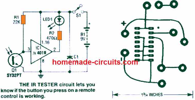 You must mount the IR phototransistor in a position where it may quickly be able to detect the IR signal, and the LED should be mounted in a place where it's easily visible.
A 9 -volt battery can be used for powering the circuit, nevertheless it is possible to replace the battery power with an AC powered supply if it is felt necessary.
After the unit is built, the tester can detect whether your IR remote control is having any sort of technical problem or not.
You just have to focus the remote control towards the IR phototransistor, and start pressing each of the buttons.
The LED will begin flashing if the remote signal is in a proper working order.
You must mount the IR phototransistor in a position where it may quickly be able to detect the IR signal, and the LED should be mounted in a place where it's easily visible.
A 9 -volt battery can be used for powering the circuit, nevertheless it is possible to replace the battery power with an AC powered supply if it is felt necessary.
After the unit is built, the tester can detect whether your IR remote control is having any sort of technical problem or not.
You just have to focus the remote control towards the IR phototransistor, and start pressing each of the buttons.
The LED will begin flashing if the remote signal is in a proper working order.
 Li-Ion batteries are one of the most advanced forms of batteries which are designed to charge and discharge at high efficiency rates, compared to any other form of batteries.
Li-Ion batteries are able to charge significantly quickly by storing the voltage and current at almost 90% efficiency, and are able to deliver the same with almost the same amount of efficiency.
That's the reason today all advanced and state-of-the-art gadgets depend on Li-Ion batteries for their functioning and performance.
In this article we are discussing the18650 2600mAh Li-Ion Cells which look quite similar to the well known traditional AAA 1.5V cells, but are a lot more powerful and efficient with their ratings.
Li-Ion batteries are one of the most advanced forms of batteries which are designed to charge and discharge at high efficiency rates, compared to any other form of batteries.
Li-Ion batteries are able to charge significantly quickly by storing the voltage and current at almost 90% efficiency, and are able to deliver the same with almost the same amount of efficiency.
That's the reason today all advanced and state-of-the-art gadgets depend on Li-Ion batteries for their functioning and performance.
In this article we are discussing the18650 2600mAh Li-Ion Cells which look quite similar to the well known traditional AAA 1.5V cells, but are a lot more powerful and efficient with their ratings.
 The above figure shows a simple18650 2600mAh Battery charger circuit using a single LM317 IC regulator and an IC 741 based opamp stages.
Rx may be calculated as given below:
Rx = 1.2 / 0.6 = 2 ohm/ 1/2 watt
If you want to use fixed resistor instead of the 4k7 preset, you can calculated the same with the following formula;
VO= VREF(1 + R2 / R1) + (IADJ¡Á R2)
where is = VREF = 1.25, R1 = 240 ohms, R2 = for 4k7 preset
Current ADJ is just 50 ¦ÌA and therefore too small to be considered in the formula, you can remove it.
Alternatively you could also try this software
The above figure shows a simple18650 2600mAh Battery charger circuit using a single LM317 IC regulator and an IC 741 based opamp stages.
Rx may be calculated as given below:
Rx = 1.2 / 0.6 = 2 ohm/ 1/2 watt
If you want to use fixed resistor instead of the 4k7 preset, you can calculated the same with the following formula;
VO= VREF(1 + R2 / R1) + (IADJ¡Á R2)
where is = VREF = 1.25, R1 = 240 ohms, R2 = for 4k7 preset
Current ADJ is just 50 ¦ÌA and therefore too small to be considered in the formula, you can remove it.
Alternatively you could also try this software
 Adjust the pot to get an exact 4.1 V at the output for the 18650 cell.
R1 = 240 ohms
D1---D4 = 1N4007
POT = 4k7 pot
C1 = 1000uF/25 V
Transformer = 0-6V/1 amp
Adjust the pot to get an exact 4.1 V at the output for the 18650 cell.
R1 = 240 ohms
D1---D4 = 1N4007
POT = 4k7 pot
C1 = 1000uF/25 V
Transformer = 0-6V/1 amp
 As we can see in the figure, two18650 2600 mAh cells are connected in series inside a compact enclosure, and the output terminal are configured for charging the desired cellphone during emergency usage.
To render the power bank in ready or stand by position, it should be first charged using a charger that is explained in the previous section of this article.
The input voltage must be set at 8.4V.
Once fully charged the power bank should be removed from the charger, during this time the battery voltage may drop to its standard level of 3.8V each constituting a total voltage of 7.6V.
The attached diodes make sure that the final output from the power bank is dropped to around 5.2V, while the 2 ohm resistor adds a current control feature to the output.
This resistor value may need to be adjusted depending on the type of cellphone connected with the output, so that the charging is optimally and efficiently implemented
Once the above standby by state achieved, this18650 2600mAh based power bank could be carried outdoors by the user for the intended emergency charging purpose.
Have questions? please ask them through the comment box below!
As we can see in the figure, two18650 2600 mAh cells are connected in series inside a compact enclosure, and the output terminal are configured for charging the desired cellphone during emergency usage.
To render the power bank in ready or stand by position, it should be first charged using a charger that is explained in the previous section of this article.
The input voltage must be set at 8.4V.
Once fully charged the power bank should be removed from the charger, during this time the battery voltage may drop to its standard level of 3.8V each constituting a total voltage of 7.6V.
The attached diodes make sure that the final output from the power bank is dropped to around 5.2V, while the 2 ohm resistor adds a current control feature to the output.
This resistor value may need to be adjusted depending on the type of cellphone connected with the output, so that the charging is optimally and efficiently implemented
Once the above standby by state achieved, this18650 2600mAh based power bank could be carried outdoors by the user for the intended emergency charging purpose.
Have questions? please ask them through the comment box below!
 The 7805 regulator and R1 provide a constant current and voltage at the base of Q1. Some designs use a zener diode for this function, but the 7805 does a great job also.
The larger voltage +9 is in series with Rh2to the emitter and the voltage at the base appears negative to the emitter, allowing emitter, base, collector current flow.
Rh2provides for adjustment of the current in milliamps through Q1 & R2 to test lead A.
The current will not exceed the constant current at the base of Q1. R2 was also added to the collector side to provide some temperature compensation for Q1. When a resistance load is connected to the test lead terminals A&B, the voltage at terminal A is connected to R3 and the input pin 2 of the 741 IC.
The combination of R3 and R4 determine the voltage gain of the opamp ( R4/R3=1000).
Pin 2 of the opamp is the inverting input, so the output at pin 6 is negative.
RH2 provides for zeroing the meter to the left side.
The negative voltage is passed through RH3 to the 1 ma full scale analog meter.
RH3 provides for calibrating the meter to the right side (full scale).
D1 & D2 offer some over voltage protection.
C2 is optional.
I added C2 to slow down my meter movement.
As the resistance is lowered across test points A & B, the voltage will also be lowered to the input of the opamp.
The meter operates just opposite of an analog ohm meter.
With only the ten 1 ohm resistors in parallel across the test leads, the meter will be at full scale to the right, indicating 0.1 ohm.
When a zero ohm resistance is connected to the test leads, the meter will move to the extreme left for zero ohms.
If you want more sensitivity to resistance, increase the parallel one ohm resistors from ten to twelve.
This will make the full scale resistance .08 ohms instead of .1.
The 7805 regulator and R1 provide a constant current and voltage at the base of Q1. Some designs use a zener diode for this function, but the 7805 does a great job also.
The larger voltage +9 is in series with Rh2to the emitter and the voltage at the base appears negative to the emitter, allowing emitter, base, collector current flow.
Rh2provides for adjustment of the current in milliamps through Q1 & R2 to test lead A.
The current will not exceed the constant current at the base of Q1. R2 was also added to the collector side to provide some temperature compensation for Q1. When a resistance load is connected to the test lead terminals A&B, the voltage at terminal A is connected to R3 and the input pin 2 of the 741 IC.
The combination of R3 and R4 determine the voltage gain of the opamp ( R4/R3=1000).
Pin 2 of the opamp is the inverting input, so the output at pin 6 is negative.
RH2 provides for zeroing the meter to the left side.
The negative voltage is passed through RH3 to the 1 ma full scale analog meter.
RH3 provides for calibrating the meter to the right side (full scale).
D1 & D2 offer some over voltage protection.
C2 is optional.
I added C2 to slow down my meter movement.
As the resistance is lowered across test points A & B, the voltage will also be lowered to the input of the opamp.
The meter operates just opposite of an analog ohm meter.
With only the ten 1 ohm resistors in parallel across the test leads, the meter will be at full scale to the right, indicating 0.1 ohm.
When a zero ohm resistance is connected to the test leads, the meter will move to the extreme left for zero ohms.
If you want more sensitivity to resistance, increase the parallel one ohm resistors from ten to twelve.
This will make the full scale resistance .08 ohms instead of .1.

 The salient features of this universal automatic battery charger are:
1) Constant voltage charging
2) Automatic cut-off when battery is fully charged.
3) Max current 5 amps, which means batteries up to 50AH can be charged with this charger normally.
4) Fully customizable as per the battery specs.
5) Low cost
6) No special parts required, all are standard and easily available.
7) LED indicators for cut-off and charging status monitoring.
8) Suitable for garages and home use.
The salient features of this universal automatic battery charger are:
1) Constant voltage charging
2) Automatic cut-off when battery is fully charged.
3) Max current 5 amps, which means batteries up to 50AH can be charged with this charger normally.
4) Fully customizable as per the battery specs.
5) Low cost
6) No special parts required, all are standard and easily available.
7) LED indicators for cut-off and charging status monitoring.
8) Suitable for garages and home use.
 Track side view

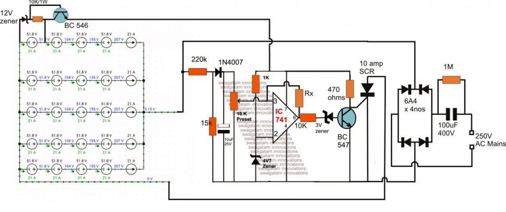 PLEASE CONNECT A 1uF/25V ACROSS PIN3 AND PIN4 OF THE IC, SO THAT THE SCR ALWAYS BEGINS WITH A MOMENTARY SWITCH ON WHENEVER THE CIRCUIT IS POWERED ON, REGARDLESS OF WHETHER THE BATTERY IS CONNECTED OR NOT.
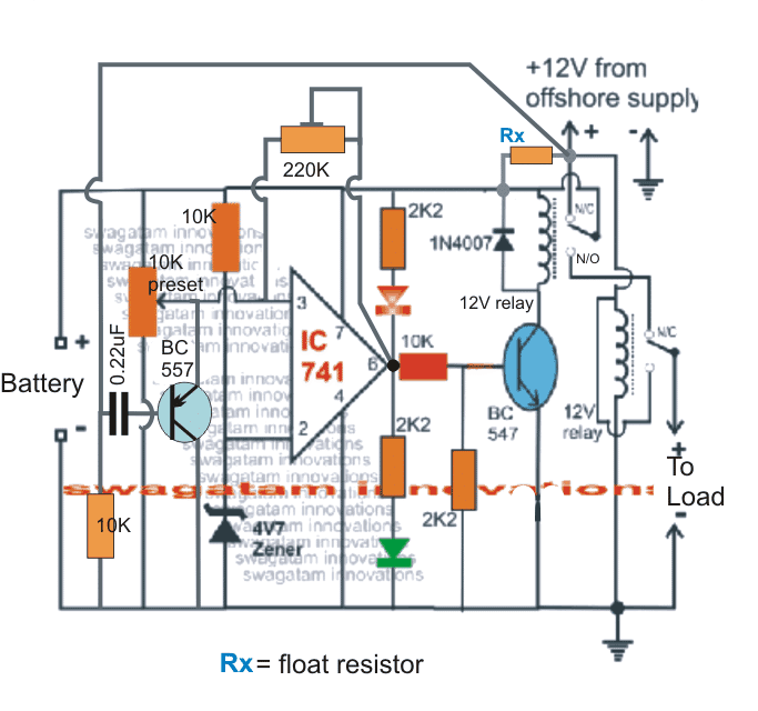
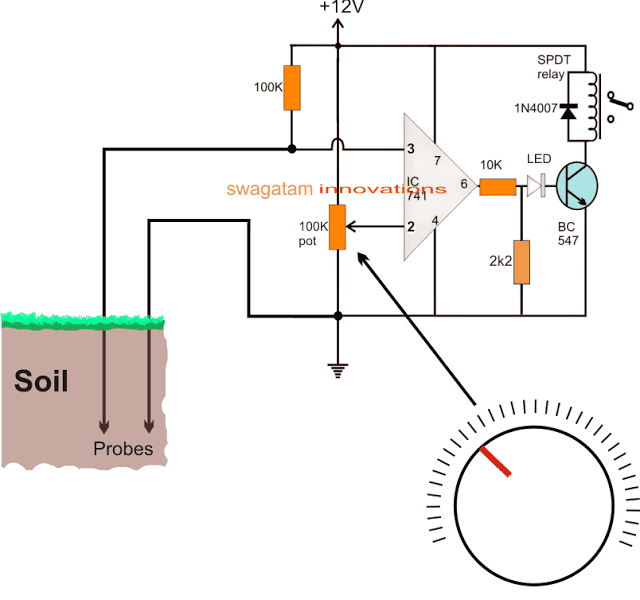 Referring to the circuit above, the design makes use of a single IC 741 opamp comparator for the required testing function.
The pin3 which is the non-inverting input of the opamp is used as the main sensor probe with respect to the other probe connected with the ground.
The moisture level present in the soil develops a resistance across it which increases with a decrease in the moisture level and decreases with an increase in the moisture level, meaning a wet soil will have a much lower resistance compared to a dryer soil.
This aspect is exploited in the design the probes are used to test the soil resistance between pin#3 and ground of the comparator IC 741.
This soil resistance forms a potential divider with the 100K resistor connected across the positive supply line and pin#3 of the IC, and the potential difference developed here in response to the soil moisture level is compared by the potential at pin#2.
Pin#2 potential is determined by the setting the shown 100k pot.
Thus this pot is effectively used for determining or verifying the exact moisture present in the soil.
If the soil moisture produces a lower resistance at pin#3 than the set level at pin#2, the output at pin#6 is rendered low, meaning when the soil is relatively wet the output of the opamp shows a zero volt, while in case the soil condition develops a higher resistance (dry condition) then the output of the opamp goes positive, triggering the connected transistor and the relay.
In other words, the output of the opamp and the relay stay switched OFF as long as as the soil moisture level is more than the threshold set by the pin#2 pot, and vice versa.
Therefore a relatively wet soil will keep the relay switched OFF, and a dry soil will switch it ON.
The LED complements the relay action and illuminates whenever the soil is dry than the desired set level.
This pot needs to be appropriately calibrated with a dial and then the various points across the dial marked as per the predetermined moisture content of a sample soil collected inside a container.
Once this is done, the calibrated pot can be used for checking any soil by simply inserting the shown probes into the soil, and by adjusting the pot until the output is rendered a high (LED ON).
Referring to the circuit above, the design makes use of a single IC 741 opamp comparator for the required testing function.
The pin3 which is the non-inverting input of the opamp is used as the main sensor probe with respect to the other probe connected with the ground.
The moisture level present in the soil develops a resistance across it which increases with a decrease in the moisture level and decreases with an increase in the moisture level, meaning a wet soil will have a much lower resistance compared to a dryer soil.
This aspect is exploited in the design the probes are used to test the soil resistance between pin#3 and ground of the comparator IC 741.
This soil resistance forms a potential divider with the 100K resistor connected across the positive supply line and pin#3 of the IC, and the potential difference developed here in response to the soil moisture level is compared by the potential at pin#2.
Pin#2 potential is determined by the setting the shown 100k pot.
Thus this pot is effectively used for determining or verifying the exact moisture present in the soil.
If the soil moisture produces a lower resistance at pin#3 than the set level at pin#2, the output at pin#6 is rendered low, meaning when the soil is relatively wet the output of the opamp shows a zero volt, while in case the soil condition develops a higher resistance (dry condition) then the output of the opamp goes positive, triggering the connected transistor and the relay.
In other words, the output of the opamp and the relay stay switched OFF as long as as the soil moisture level is more than the threshold set by the pin#2 pot, and vice versa.
Therefore a relatively wet soil will keep the relay switched OFF, and a dry soil will switch it ON.
The LED complements the relay action and illuminates whenever the soil is dry than the desired set level.
This pot needs to be appropriately calibrated with a dial and then the various points across the dial marked as per the predetermined moisture content of a sample soil collected inside a container.
Once this is done, the calibrated pot can be used for checking any soil by simply inserting the shown probes into the soil, and by adjusting the pot until the output is rendered a high (LED ON).
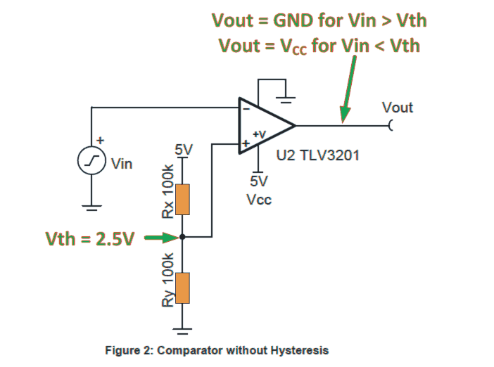 The comparator would evaluate and compare the input signal or the voltage (Vln) to the set threshold voltage (Vth).
The comparator input feed voltage which is to be compared is connected to the inverting input, as a result the output is going to feature an inverted polarity.
Each time the Vin > Vth the output is supposed to get close to the negative supply (GND or logic low for the shown diagram).
and when Vln < Vth the output would get close to the positive supply (Vcc = 5V or logic high in this example).
This easy solution enables you to decide whether or not a genuine signal for example temperature is above a given decisive threshold limit.
Even so, using this technique may possess a predicament.
Interference on the input feed signal could potentially cause the input to changeovers above and below the set threshold triggering an inconsistent or fluctuating output results.
The comparator would evaluate and compare the input signal or the voltage (Vln) to the set threshold voltage (Vth).
The comparator input feed voltage which is to be compared is connected to the inverting input, as a result the output is going to feature an inverted polarity.
Each time the Vin > Vth the output is supposed to get close to the negative supply (GND or logic low for the shown diagram).
and when Vln < Vth the output would get close to the positive supply (Vcc = 5V or logic high in this example).
This easy solution enables you to decide whether or not a genuine signal for example temperature is above a given decisive threshold limit.
Even so, using this technique may possess a predicament.
Interference on the input feed signal could potentially cause the input to changeovers above and below the set threshold triggering an inconsistent or fluctuating output results.
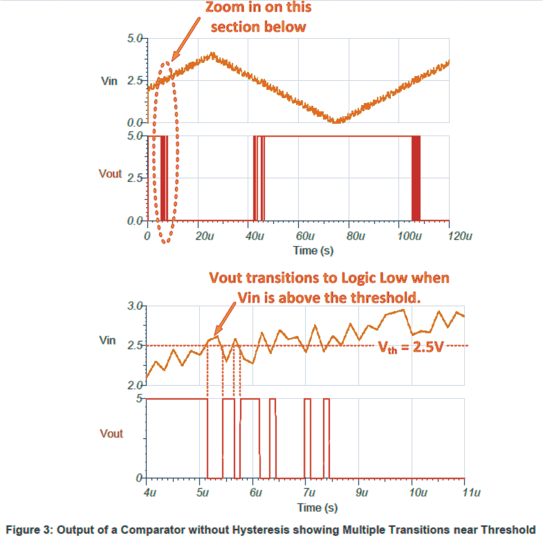 While the input signal voltage arrives the set limit (by the voltage divider network) (Vth = 2.5V), it adjusts above as well as below the minimum threshold a number of instances.
As a result, the output fluctuates too in accordance with the input.
In actual circuits, this unstable output may easily cause unfavorable issues.
As an illustration, think about the input signal to be a temperature parameter and the output response to be a crucial temperature based application, which happens to be interpreted by a microcontroller.
The fluctuating output signal response may not contribute a faithful information to the microcontroller and could produce "confusing" results for the microcontroller at the crucial threshold levels.
Additionally, imagine that the comparator output is required to operate a motor or valve.
This inconsistent switching during the threshold limits could force the valve or motor to be switched ON/OFF many times in the course of the crucial threshold situations..
But a "cool" solution through a modest alteration to the comparator circuit enables you to include hysteresis which in turn completely eliminates the jittery output during threshold changeovers.
Hysteresis takes advantage of a couple of distinct threshold voltage limits to stay clear from the fluctuating transitions as seen in the discussed circuit.
The input signal feed needs to go over the upper threshold (VH) to generate a changeover of a low output or below the lower set threshold limit (VL) to switch over to a high output.
While the input signal voltage arrives the set limit (by the voltage divider network) (Vth = 2.5V), it adjusts above as well as below the minimum threshold a number of instances.
As a result, the output fluctuates too in accordance with the input.
In actual circuits, this unstable output may easily cause unfavorable issues.
As an illustration, think about the input signal to be a temperature parameter and the output response to be a crucial temperature based application, which happens to be interpreted by a microcontroller.
The fluctuating output signal response may not contribute a faithful information to the microcontroller and could produce "confusing" results for the microcontroller at the crucial threshold levels.
Additionally, imagine that the comparator output is required to operate a motor or valve.
This inconsistent switching during the threshold limits could force the valve or motor to be switched ON/OFF many times in the course of the crucial threshold situations..
But a "cool" solution through a modest alteration to the comparator circuit enables you to include hysteresis which in turn completely eliminates the jittery output during threshold changeovers.
Hysteresis takes advantage of a couple of distinct threshold voltage limits to stay clear from the fluctuating transitions as seen in the discussed circuit.
The input signal feed needs to go over the upper threshold (VH) to generate a changeover of a low output or below the lower set threshold limit (VL) to switch over to a high output.
 Each time the output is at a logic high (5V), Rh remains in parallel with Rx.
This pushes extra current into Ry, elevating the threshold limit voltage (VH) to 2.7V.
The input signal will likely need to go above VH=2.7V to prompt the output response to move to a logic low (0V).
While the output is at logic low (0V), Rh is set parallel with Ry.
This cuts-down on the current into Ry, bringing down the threshold voltage to 2.3V.
The input signal will want to go below VL=2.3V to settle the output to a logic high (5V).
Each time the output is at a logic high (5V), Rh remains in parallel with Rx.
This pushes extra current into Ry, elevating the threshold limit voltage (VH) to 2.7V.
The input signal will likely need to go above VH=2.7V to prompt the output response to move to a logic low (0V).
While the output is at logic low (0V), Rh is set parallel with Ry.
This cuts-down on the current into Ry, bringing down the threshold voltage to 2.3V.
The input signal will want to go below VL=2.3V to settle the output to a logic high (5V).
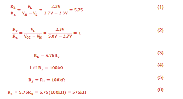
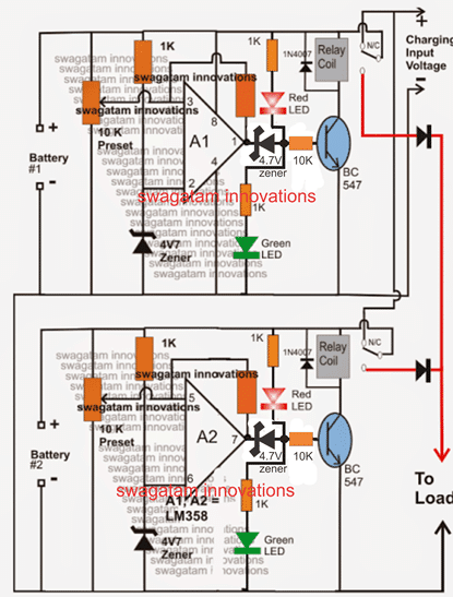 Why are 4.7 zeners being used for the reference voltage? If we don't want the 12 volts to drop below 11 for discharge,why such a low zener value?
Is the feed back resistor going to the virtual ground point a 100K resistor? If so, why was this value chosen?
Thanks for any help!
2) Also, I apologize, I forgot to as why are there 4.7 zenersat the bases of the BC 547 transistors?
3) Also my last question for today for this circuit.The red/green indication LEDs; how do they light up? I mean the red LED is connected through its resistor to the top + rail, connects to the output of the OPAMP, then goes down in series towards the green LED.
It would seem they wouldbe both on at the same time, since they are in series, in both circuits.
Does it have something to do with the feedback circuit and virtual ground? Oh I think I may see.
So when the OPAMP is off, the top red LED
Current is going through the feedback resistor (thus its "on")to the virtual ground point? But how does it get switched off, when the OPAMP has an output? When the OP AMP gets an output, I can see that going down to the green LED, but how, in that state, does the red LED then get switched off?
Thanks again for any help!
My Reply
4.7 is not a fixed value it can be changed to other values also, the pin#3 preset ultimately adjusts and calibrates the threshold as per the selecte zener value.
Question
So the reference voltage is the zener is at pin 2 (top view opamp) correct? The 100K feedback resistor and pot are creating the hysteresis value (meaning, the difference between pin 2 and 3 to make the opamp swing high to its + rail voltage)?
The opamp in this config is always trying to make pins 2 and 3 arrive at the same value via its feedback resistor, correct (zero, since the feedback divider is @ 0 and pin 3 is @ ground)?
I've seen this solar charger controller done without the feed back, just using several opamps with voltage reference pins and a pot on the other one.
I am just trying to understand how hysteresis is working in this case I don't understand the math in this circuit.
Is the 100k 10k preset feedback absolutely necessary?
In other opamp circuits, they dont use any feed back just use them in comparator config mode with ref voltage at invert/non invert pin, and when one is exceeded, the opamp swings to its rail voltage
What is the feed back doing? I understand the opamp gain formula, in this case is it 100k/10k x voltage difference of POT voltage (preset)value and 4.7 zener?
Or is this a Schmidt trigger type of hysteresis UTP LTP circuit
I still don't get the feed back with the 100k/10k; most opamp comparators Ive seen just use the opamp in saturation, could you explain why the feedback and gain for this?
Ok I am goofed; the 10K preset is used to divide the voltage from the 12volt rail, correct? So, when its preset value according to the POT wiper is more? than the 4.7V zener, we swing the opamp high? still dont get the 100k feedback and why its used in a comparator circuit
Why are 4.7 zeners being used for the reference voltage? If we don't want the 12 volts to drop below 11 for discharge,why such a low zener value?
Is the feed back resistor going to the virtual ground point a 100K resistor? If so, why was this value chosen?
Thanks for any help!
2) Also, I apologize, I forgot to as why are there 4.7 zenersat the bases of the BC 547 transistors?
3) Also my last question for today for this circuit.The red/green indication LEDs; how do they light up? I mean the red LED is connected through its resistor to the top + rail, connects to the output of the OPAMP, then goes down in series towards the green LED.
It would seem they wouldbe both on at the same time, since they are in series, in both circuits.
Does it have something to do with the feedback circuit and virtual ground? Oh I think I may see.
So when the OPAMP is off, the top red LED
Current is going through the feedback resistor (thus its "on")to the virtual ground point? But how does it get switched off, when the OPAMP has an output? When the OP AMP gets an output, I can see that going down to the green LED, but how, in that state, does the red LED then get switched off?
Thanks again for any help!
My Reply
4.7 is not a fixed value it can be changed to other values also, the pin#3 preset ultimately adjusts and calibrates the threshold as per the selecte zener value.
Question
So the reference voltage is the zener is at pin 2 (top view opamp) correct? The 100K feedback resistor and pot are creating the hysteresis value (meaning, the difference between pin 2 and 3 to make the opamp swing high to its + rail voltage)?
The opamp in this config is always trying to make pins 2 and 3 arrive at the same value via its feedback resistor, correct (zero, since the feedback divider is @ 0 and pin 3 is @ ground)?
I've seen this solar charger controller done without the feed back, just using several opamps with voltage reference pins and a pot on the other one.
I am just trying to understand how hysteresis is working in this case I don't understand the math in this circuit.
Is the 100k 10k preset feedback absolutely necessary?
In other opamp circuits, they dont use any feed back just use them in comparator config mode with ref voltage at invert/non invert pin, and when one is exceeded, the opamp swings to its rail voltage
What is the feed back doing? I understand the opamp gain formula, in this case is it 100k/10k x voltage difference of POT voltage (preset)value and 4.7 zener?
Or is this a Schmidt trigger type of hysteresis UTP LTP circuit
I still don't get the feed back with the 100k/10k; most opamp comparators Ive seen just use the opamp in saturation, could you explain why the feedback and gain for this?
Ok I am goofed; the 10K preset is used to divide the voltage from the 12volt rail, correct? So, when its preset value according to the POT wiper is more? than the 4.7V zener, we swing the opamp high? still dont get the 100k feedback and why its used in a comparator circuit
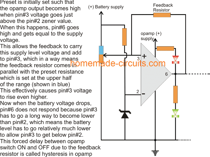
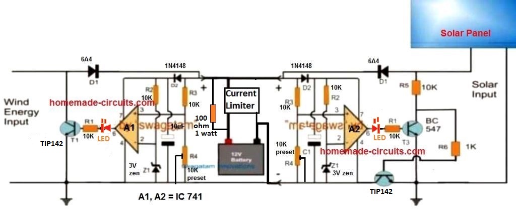 The figure above shows the proposed solar, wind twin hybrid battery charger circuit, using very ordinary components such as opamps and transistors.
We can see two exactly similar opamp stages being employed, one on the left side of the battery and the other on the right side of the battery.
The left side opamp stage becomes responsible for accepting and regulating the wind energy source while the right side opamp stage processes the solar electricity for charging the single common battery in the middle.
Although the two stages look similar, the modes of regulation are different.
The wind energy controller circuit regulates the wind energy by shunting or shorting the excess energy to ground, while the solar processor stage does the same but by cutting of the excess energy instead of shunting.
The above explained two modes are crucial since in wind generators which are essentially alternators require the excess energy to be shunted, and not cut off, so that the coil inside can be safeguarded from over current, which also keeps the speed of the alternator at a controlled rate.
This implies that the concept can be also implemented in ELC applications also.
The figure above shows the proposed solar, wind twin hybrid battery charger circuit, using very ordinary components such as opamps and transistors.
We can see two exactly similar opamp stages being employed, one on the left side of the battery and the other on the right side of the battery.
The left side opamp stage becomes responsible for accepting and regulating the wind energy source while the right side opamp stage processes the solar electricity for charging the single common battery in the middle.
Although the two stages look similar, the modes of regulation are different.
The wind energy controller circuit regulates the wind energy by shunting or shorting the excess energy to ground, while the solar processor stage does the same but by cutting of the excess energy instead of shunting.
The above explained two modes are crucial since in wind generators which are essentially alternators require the excess energy to be shunted, and not cut off, so that the coil inside can be safeguarded from over current, which also keeps the speed of the alternator at a controlled rate.
This implies that the concept can be also implemented in ELC applications also.
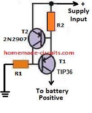 R2 may be calculated with the following formula:
R2 = 0.7 / charging current
wattage of the resistor = 0.7 x charging current
R2 may be calculated with the following formula:
R2 = 0.7 / charging current
wattage of the resistor = 0.7 x charging current
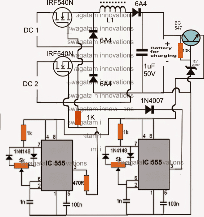

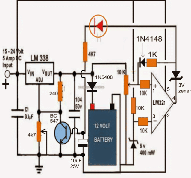
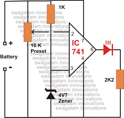
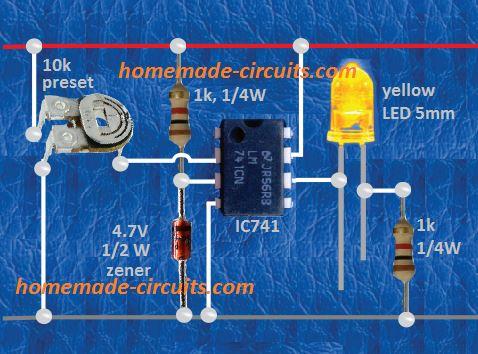 The above circuit can be modified by adding a relay stage for controlling a particular stage which may be relevant to the low battery cut of actions.
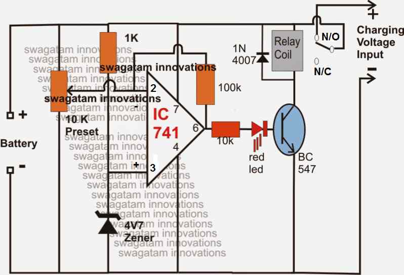
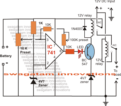 The 4.7 V zener at the transistor emitter is not essential.
Please replace it with a direct link
The 4.7 V zener at the transistor emitter is not essential.
Please replace it with a direct link
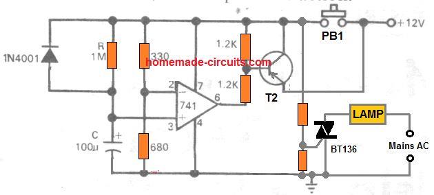 The two triac gate resistors can be 1K each
Referring to the figure, we see that the inverting input is set to about 2/3 rd of the supply voltage.
This voltage level in fact becomes the reference source to the IC.
The non inverting input pin of the IC is connected to the unction of a RC network, where the other end of the resistor R (variable if required) is connected to the positive supply and the negative pin of the capacitor C goes to the ground point of the circuit.
Powering the circuit is rather done in an interesting manner.
Here the transistor T2 along with PB1 is so wired that on pressing PB1, T2 latches and holds the supply voltage to keep the circuit powered.
Now, initially the voltage at pin #3 is almost at the ground potential because of C, however as C charges the potential at this pin of the IC starts rising.
Depending upon the value of R, after a particular length of time C charges itself to a level which may be above 2/3 rd of the supply voltage as set at the inverting input.
The IC responds and immediately toggles its output to produce a logic high or a positive voltage.
T1 and the triac at the output deactivates and switches of the external load connected to it.
The high logic at the output of the IC also inhibits T2 from conducting and breaks the latch to switch of the whole system.
The timing sequence of this bedroom lamp timer can be repeated or initiated by pressing PB1 whenever felt necessary.
The two triac gate resistors can be 1K each
Referring to the figure, we see that the inverting input is set to about 2/3 rd of the supply voltage.
This voltage level in fact becomes the reference source to the IC.
The non inverting input pin of the IC is connected to the unction of a RC network, where the other end of the resistor R (variable if required) is connected to the positive supply and the negative pin of the capacitor C goes to the ground point of the circuit.
Powering the circuit is rather done in an interesting manner.
Here the transistor T2 along with PB1 is so wired that on pressing PB1, T2 latches and holds the supply voltage to keep the circuit powered.
Now, initially the voltage at pin #3 is almost at the ground potential because of C, however as C charges the potential at this pin of the IC starts rising.
Depending upon the value of R, after a particular length of time C charges itself to a level which may be above 2/3 rd of the supply voltage as set at the inverting input.
The IC responds and immediately toggles its output to produce a logic high or a positive voltage.
T1 and the triac at the output deactivates and switches of the external load connected to it.
The high logic at the output of the IC also inhibits T2 from conducting and breaks the latch to switch of the whole system.
The timing sequence of this bedroom lamp timer can be repeated or initiated by pressing PB1 whenever felt necessary.
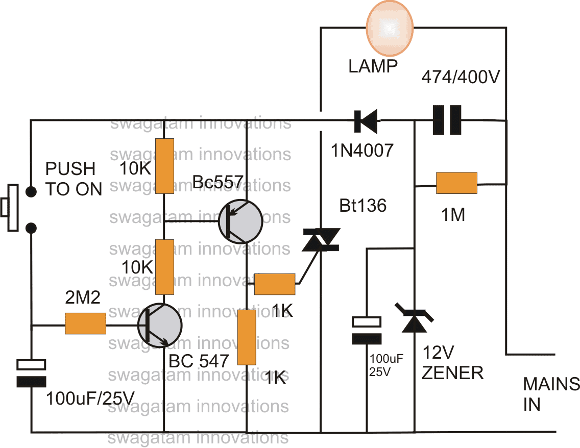 WARNING: All the circuit concepts presented above are not isolated from the mains AC, and therefore touching the elements in the powered condition can be fatal.
Necessary precautions are strictly advised.
Make sure to use a plastic enclosure for the circuit once the working of the finalized design is confirmed.
WARNING: All the circuit concepts presented above are not isolated from the mains AC, and therefore touching the elements in the powered condition can be fatal.
Necessary precautions are strictly advised.
Make sure to use a plastic enclosure for the circuit once the working of the finalized design is confirmed.
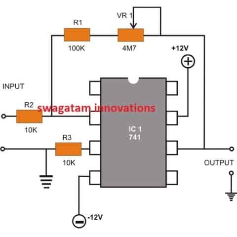 Sometimes it becomes important for amplifying DC voltages, the diagram above shows how the IC can be wired up into an inverting DC amplifier circuit.
As the name informs a DC input to the IC will be amplified at its output but will be just the opposite with polarity.
VR1 may be used for adjusting the gain of the amplifier.
Sometimes it becomes important for amplifying DC voltages, the diagram above shows how the IC can be wired up into an inverting DC amplifier circuit.
As the name informs a DC input to the IC will be amplified at its output but will be just the opposite with polarity.
VR1 may be used for adjusting the gain of the amplifier.
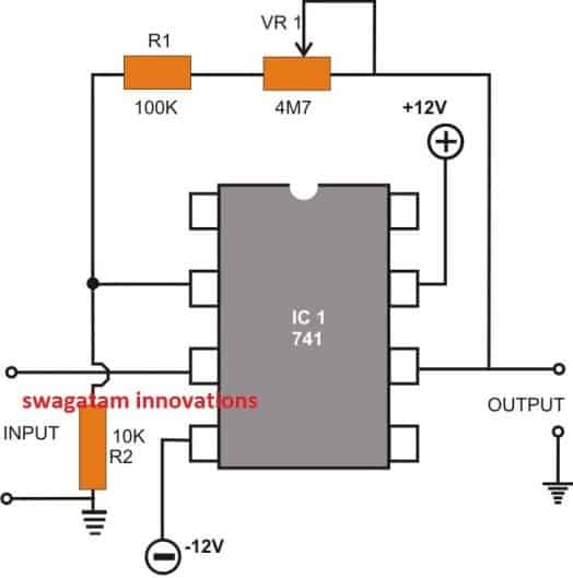 This configuration is similar to the above circuit, the only difference being the output response, which is always equal to the polarity of the fed input voltage.
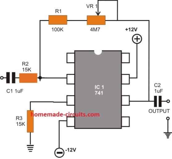 The figure shows how the basic inverting DC mode of the IC can be simply modified into an inverting AC amplifier design.
This circuit is intended to be used with AC or oscillating input signals, primarily for amplifying minute frequencies.
C1 and C2 form the input and the output coupling capacitors.
Again here the gain may be varied using the pot VR1.
The figure shows how the basic inverting DC mode of the IC can be simply modified into an inverting AC amplifier design.
This circuit is intended to be used with AC or oscillating input signals, primarily for amplifying minute frequencies.
C1 and C2 form the input and the output coupling capacitors.
Again here the gain may be varied using the pot VR1.
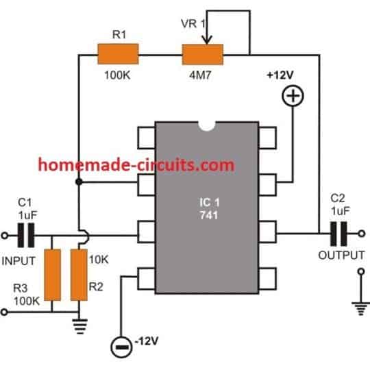 The 741 op amp circuit is similar to the above explained design; the only difference being the output of the circuit provides oscillations in phase with the input whereas the previous design produces oscillations with opposite phase to that of the input.
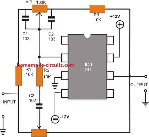 The opamp IC741 can be very effectively used for processing audio frequencies and customizing them as per one¡¯s own choice.
Folks who prefer more bass in music may achieve it by just adjusting the bass control shaft whereas those who appreciate extra treble with music may do the same through another similar control reserved for the purpose.
The circuit diagram shows how by adding just a few passive components with the IC 741 a neat little active tone control circuit can be built.
For the given values, the circuit provides a bass boost of 12.5 dB and a cut of 10.5 dB at around 100 Hz.
The treble chill is of 8.8 dB with a cut of 9.8 dB at around 10 kHz, with respect to the set gain of the device at 1 kHz.
The circuit also features high input impedance and low output impedance.
The opamp IC741 can be very effectively used for processing audio frequencies and customizing them as per one¡¯s own choice.
Folks who prefer more bass in music may achieve it by just adjusting the bass control shaft whereas those who appreciate extra treble with music may do the same through another similar control reserved for the purpose.
The circuit diagram shows how by adding just a few passive components with the IC 741 a neat little active tone control circuit can be built.
For the given values, the circuit provides a bass boost of 12.5 dB and a cut of 10.5 dB at around 100 Hz.
The treble chill is of 8.8 dB with a cut of 9.8 dB at around 10 kHz, with respect to the set gain of the device at 1 kHz.
The circuit also features high input impedance and low output impedance.
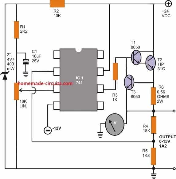 The final diagram of this article shows a classic stabilized voltage DC power supply using 741 opamp circuit design.
A cheap zener / resistor voltage reference is used to provide a reasonably stable reference to the non-inverting input of the IC.
The pot VR 1 is used to set the output voltage right from zero to a maximum of 15 volts continuously.
A Darlington pair transistor is used at the output to enhance high current delivering capacity.
However another transistor T3 has also been incorporated to check the above current if it tends to drift beyond limit.
The control limit may be set by varying the value of the resistor R6.
The final diagram of this article shows a classic stabilized voltage DC power supply using 741 opamp circuit design.
A cheap zener / resistor voltage reference is used to provide a reasonably stable reference to the non-inverting input of the IC.
The pot VR 1 is used to set the output voltage right from zero to a maximum of 15 volts continuously.
A Darlington pair transistor is used at the output to enhance high current delivering capacity.
However another transistor T3 has also been incorporated to check the above current if it tends to drift beyond limit.
The control limit may be set by varying the value of the resistor R6.
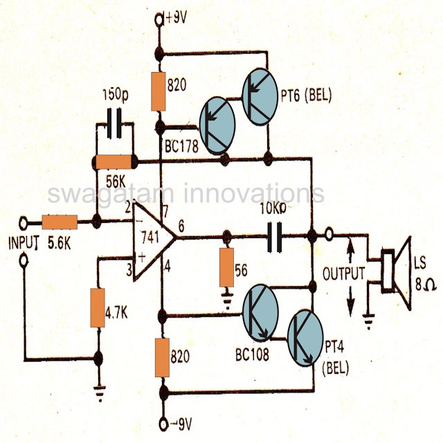 Though the maximum power of this amplifier is not more than 4 watts, the amplifier provides relatively good response with the applied frequency.The distortion of less than 0.5% and has a bandwidth of over 20kHz.
The amplifier requires a minimum input ofaround 150 mV.
Though the maximum power of this amplifier is not more than 4 watts, the amplifier provides relatively good response with the applied frequency.The distortion of less than 0.5% and has a bandwidth of over 20kHz.
The amplifier requires a minimum input ofaround 150 mV.
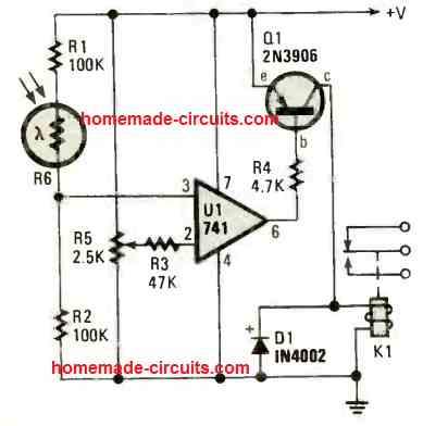 If you would like it to use anything more substantial, select a relay having contacts that can handle the voltage (and current) equivalent to the load wattage.
It's exactly that easy.
Just be sure the relay coil is rated not less than 150 ohms.
With standard brightness, the R6 LDR's resistance will be low.
The input potential at pin 3 of IC U1 will be high, which will cause a high at the output at pin 6.
Since the transistor Q1 is a PNP transistor, and the collector current will be reduced as long as the pin6 of the IC 741 holds it base positive.
As soon as light source to the LDR becomes low or when darkness sets in, the R6 LDR resistance increases.
In this situation Pin 3 of the IC 741 turns in a negative course, causing the output of IC 741 at pin 6 to become low or around zero voltage.
This situation resources the required negative base current to Q1 base via the 4k7 resistor, R4. Collector current of the transistor now increases, and the relay gets instantly activated.
When the relay gets activated, the connected lamp or any load turns ON.
If you would like it to use anything more substantial, select a relay having contacts that can handle the voltage (and current) equivalent to the load wattage.
It's exactly that easy.
Just be sure the relay coil is rated not less than 150 ohms.
With standard brightness, the R6 LDR's resistance will be low.
The input potential at pin 3 of IC U1 will be high, which will cause a high at the output at pin 6.
Since the transistor Q1 is a PNP transistor, and the collector current will be reduced as long as the pin6 of the IC 741 holds it base positive.
As soon as light source to the LDR becomes low or when darkness sets in, the R6 LDR resistance increases.
In this situation Pin 3 of the IC 741 turns in a negative course, causing the output of IC 741 at pin 6 to become low or around zero voltage.
This situation resources the required negative base current to Q1 base via the 4k7 resistor, R4. Collector current of the transistor now increases, and the relay gets instantly activated.
When the relay gets activated, the connected lamp or any load turns ON.
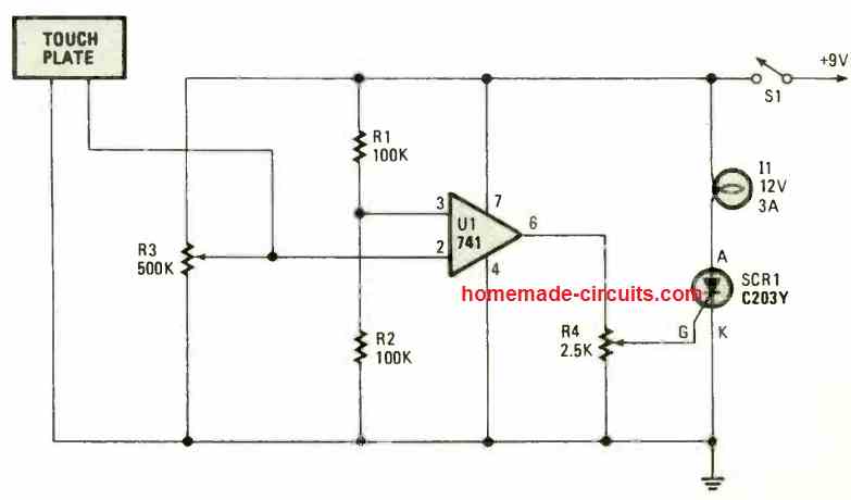 In the normal situation the SCR remains in the switched OFF condition, keeping the lamp shut off.
When pin6 turns positive due to touching of the touch plate, causes the SCR gate go positive, and the SCR fires and conducts and gets latched, switching ON the lamp, which is kept switched ON until the power supply to the circuit is turned OFF by S1.
In the normal situation the SCR remains in the switched OFF condition, keeping the lamp shut off.
When pin6 turns positive due to touching of the touch plate, causes the SCR gate go positive, and the SCR fires and conducts and gets latched, switching ON the lamp, which is kept switched ON until the power supply to the circuit is turned OFF by S1.
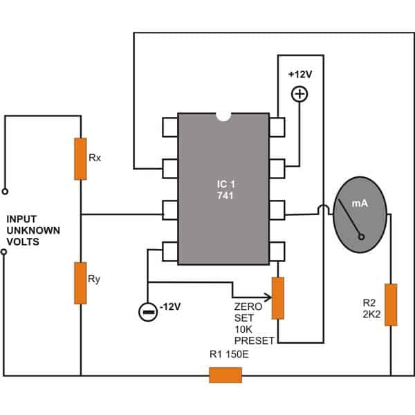 A simple configuration for measuring DC voltages is shown above using the IC 741.
A couple of resistors Rx and Ry are introduced at the input in a potential divider mode at the non-inverting pin #3 of the IC.
The voltage to be measured is applied across the resistor R1 and ground.
Through proper selection of Rx and Ry, the range of the meter can be varied and different voltages can be measured.
A simple configuration for measuring DC voltages is shown above using the IC 741.
A couple of resistors Rx and Ry are introduced at the input in a potential divider mode at the non-inverting pin #3 of the IC.
The voltage to be measured is applied across the resistor R1 and ground.
Through proper selection of Rx and Ry, the range of the meter can be varied and different voltages can be measured.
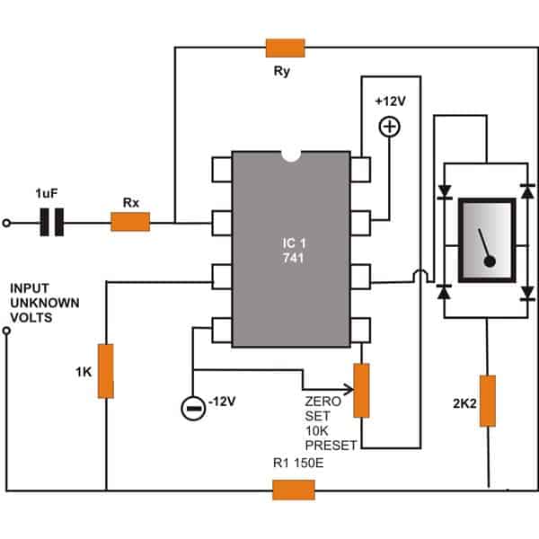 In case you want to measure alternating voltages then the circuit illustrated above can become useful.
The wiring is similar to the above wiring, however the positions of Rx and Ry have changed and also a coupling capacitor comes into the scene at the inverting input of the IC.
Interestingly the meter here is now connected across a bridge network enabling the meter to display the relevant AC potentials correctly.
In case you want to measure alternating voltages then the circuit illustrated above can become useful.
The wiring is similar to the above wiring, however the positions of Rx and Ry have changed and also a coupling capacitor comes into the scene at the inverting input of the IC.
Interestingly the meter here is now connected across a bridge network enabling the meter to display the relevant AC potentials correctly.
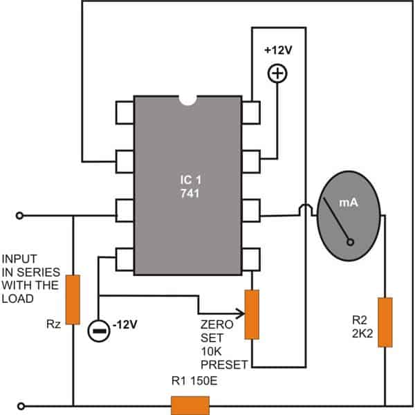 .
.
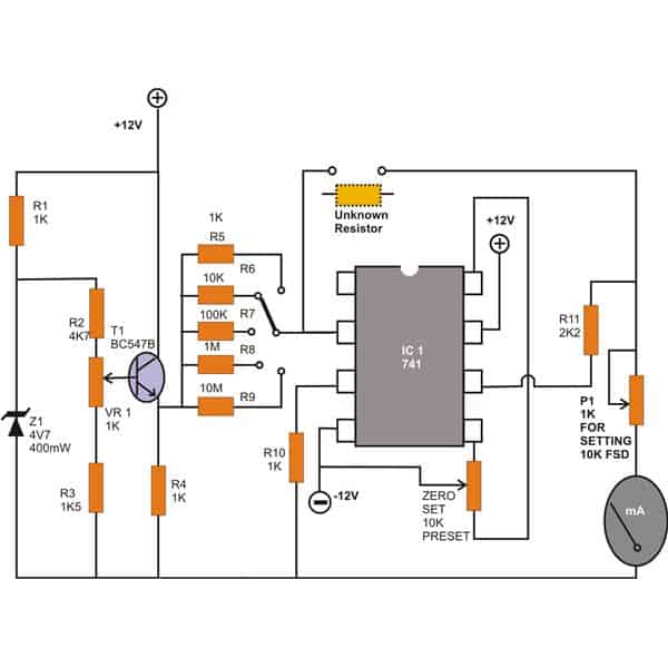 Unlike most of the analogue designs which tend to have a rather non-linear behavior, the present design very efficiently tackles the problem to produce a perfectly linear response with the corresponding measurements.
The range is pretty impressive, it can measure values of resistors right from 1K up to a staggering 10 M.
You may go on to modify the circuit for enabling the measurement of more extreme values.
The range is selected by moving the rotary switch switch into the relevant positions.
Unlike most of the analogue designs which tend to have a rather non-linear behavior, the present design very efficiently tackles the problem to produce a perfectly linear response with the corresponding measurements.
The range is pretty impressive, it can measure values of resistors right from 1K up to a staggering 10 M.
You may go on to modify the circuit for enabling the measurement of more extreme values.
The range is selected by moving the rotary switch switch into the relevant positions.
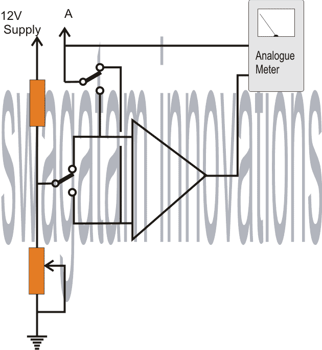
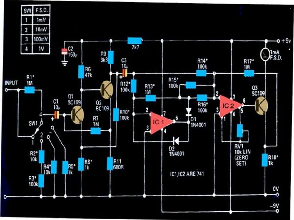
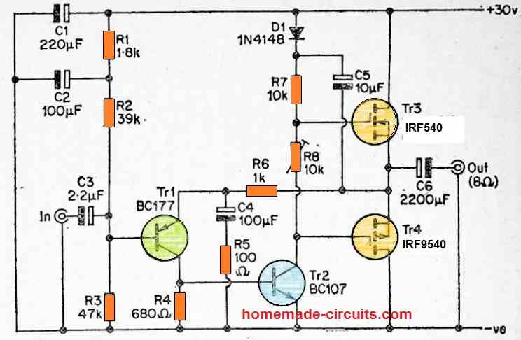
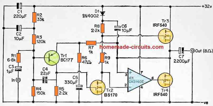 During the time theoutput is negative going, the load is powered by Tr3 in common source mode, which, like the earlier circuit, provides good performance on negative going outputs.
Tr3 is accompanied by an operational amplifier whose non-inverting input is linked to the amplifier's output (Tr3 and Tr4 sources).
Given that the signal is reversed via Tr4, this results in 100% negative feedback between Tr4 and 1C1.
This results in unity voltage gain from 1C1's inverting input to the amplifier's output, resulting in a fairly decent match to Tr3. There is a little discrepancy since Tr4 and 1C1 yield almost precise unity, but the voltage gain of Tr3 (as previously described) will be substantially lowerthan unity.
However, because the circuit features a significant amount of general negative feedback to balance out the mismatch and assure minimumdistortion levels, this is of little actual significance.
1C1 is a kind with a PMOS input stage, and as a result, it has a very high input impedance, equivalent to a MOSFETdevice.
During the time theoutput is negative going, the load is powered by Tr3 in common source mode, which, like the earlier circuit, provides good performance on negative going outputs.
Tr3 is accompanied by an operational amplifier whose non-inverting input is linked to the amplifier's output (Tr3 and Tr4 sources).
Given that the signal is reversed via Tr4, this results in 100% negative feedback between Tr4 and 1C1.
This results in unity voltage gain from 1C1's inverting input to the amplifier's output, resulting in a fairly decent match to Tr3. There is a little discrepancy since Tr4 and 1C1 yield almost precise unity, but the voltage gain of Tr3 (as previously described) will be substantially lowerthan unity.
However, because the circuit features a significant amount of general negative feedback to balance out the mismatch and assure minimumdistortion levels, this is of little actual significance.
1C1 is a kind with a PMOS input stage, and as a result, it has a very high input impedance, equivalent to a MOSFETdevice.
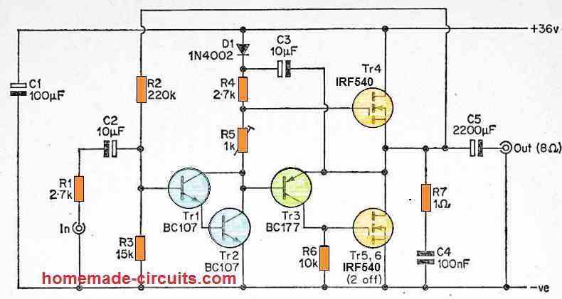 The Darlington pair emitter follower works withoutinversion of phaseand provides a voltage gain of about unity.
There is no net phase shift since the two emitter follower amplifiers individually create a phase inversion.
They effectively yield around unity voltage gain as a result of ahigh degree of feedback.
Consequently, this approach produces a fairly nice and symmetrical outcomes, even though genuine complimentary configurations are now feasible and commonly implemented.
Tr4 essentially substitutes the Darlington emitter follower stage in this circuit, Tr5/6 is the common sourceoutput transistor, and Tr3 is the common emitter complementary transistor for Tr5/6. R6 serves as Tr3's collector load, and obtaining 100 percent negative feedback is as simple as connecting Tr3's emitter to the amplifier's output.
The Darlington pair emitter follower works withoutinversion of phaseand provides a voltage gain of about unity.
There is no net phase shift since the two emitter follower amplifiers individually create a phase inversion.
They effectively yield around unity voltage gain as a result of ahigh degree of feedback.
Consequently, this approach produces a fairly nice and symmetrical outcomes, even though genuine complimentary configurations are now feasible and commonly implemented.
Tr4 essentially substitutes the Darlington emitter follower stage in this circuit, Tr5/6 is the common sourceoutput transistor, and Tr3 is the common emitter complementary transistor for Tr5/6. R6 serves as Tr3's collector load, and obtaining 100 percent negative feedback is as simple as connecting Tr3's emitter to the amplifier's output.
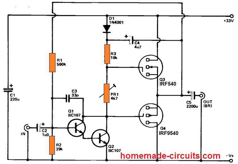 Because MOSFET devices are not vulnerabletothermal runaway, the thermal compensation circuitry is completely unneeded in this design.
In reality, when the output MOSFETsbecome hot, the quiescent bias current drops significantly, althoughnot enough to cause substantial crossover distortion.
C1 is a supply decoupling component, whereas C2 and C5 offer DC blocking at the input and output, correspondingly.
C3 contributes to the circuit's stability by attenuating high frequencies.
Despite the fact that the current in the driver stage is only approximately 1mA, it should be enough because MOSFETs have exceptionally high input impedances and use no substantial input current.
This is one of their primary benefits compared to theBJTs.
One drawback ofthis amplifier circuitis itspoorer efficiency owing to greater threshold voltages,and higheron resistance of MOSFETs when compared to bipolar devices.
Nonetheless, with a supply voltage of around 33 V or such, the circuit can provide an output of 10 Wattrms (with a current consumptionof up to approximately600mA).
For peak power, an input of around 500mV rms is required.
Because MOSFET devices are not vulnerabletothermal runaway, the thermal compensation circuitry is completely unneeded in this design.
In reality, when the output MOSFETsbecome hot, the quiescent bias current drops significantly, althoughnot enough to cause substantial crossover distortion.
C1 is a supply decoupling component, whereas C2 and C5 offer DC blocking at the input and output, correspondingly.
C3 contributes to the circuit's stability by attenuating high frequencies.
Despite the fact that the current in the driver stage is only approximately 1mA, it should be enough because MOSFETs have exceptionally high input impedances and use no substantial input current.
This is one of their primary benefits compared to theBJTs.
One drawback ofthis amplifier circuitis itspoorer efficiency owing to greater threshold voltages,and higheron resistance of MOSFETs when compared to bipolar devices.
Nonetheless, with a supply voltage of around 33 V or such, the circuit can provide an output of 10 Wattrms (with a current consumptionof up to approximately600mA).
For peak power, an input of around 500mV rms is required.
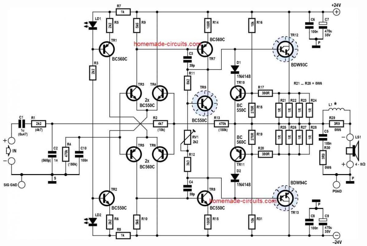 To start with, the configuration of the amplier is done in the inverting conguration, instead of implementing the common style of a non-inverting layout.
As a result, it is important to connect the speaker with reversed polarity.
However inverting ampliers don't need to perform too much to rectify the open-loop phase shifts, simply like their own non-inverting counterparts which is distinctly an advantage in this straightforward design.
Furthermore, the input capacitor in this design performs a dual function.
It delivers AC coupling and also minimizes DC gain to unity.
To be precise , all frequency dependence is maintained external to the feedback loop here.
Thus the signal stays entirely pre-conditioned through the given passive input network in order to reduce some more number of parts.
The fundamental amplier design, consequently, works using a high gain for frequencies which may be outside of the normal music frequency range.
And you can also find that apart from the 39 pF frequency compensation capacitors along with a few essential decoupling, the amplifier circuit isn't rigged with strange RC networks ¡¯in order to get stability¡¯.
Even with the above discussed parameters, this 60 watt amplier design includes a hypothetical 40¡ã phase margin, while the stream-lined PCB design helps to keep stray signal influences to a lowest level.
This is especially due to a discrete design of the power op-amp.
Almost all assessments for the amplifier had been carried out using partly unshielded test probes within an workshop atmosphere which had a lot of electrical noises.
Even in such situation, the amplifier prototype revealed absolutely no tendencies of instability.
In earlier times, the majority of amplifiers were being made with fairly small input sensitivity (1Vrms) for the integration with the line level input sources.
If you want to configure this amplifier in this way then you can do so by using the component values that are displayed in parentheses, and this will provide a gain of x12 or 22 dB.
However, the fact is that, in these modern times line-level sources are hardly seen in comparison to the low-level headphone output jacks available in smartphones and tablets.
The 60 watt amplifier circuit discussed here offers a gain of 36 dB (x67) that makes it possible for 100 % power output from all standard contemporary headphone jacks (0.2 Vrms).
The damping element is negatively impacted with increased frequencies.
Another great thing is the LED used for biasing of the current source transistors.
LEDs are used since these devices produce reduced noise compared to zener diodes, which helps to get rid of a couple of bypass capacitors, which also allows lower thermal drift for the amplifier's power switch ON!
Additionally price is less for this design along with compact and sleek nature can be observed for the emitter resistors of the power transistors, where we can find the regular 1-Q types are connected in parallel, providing an extra advantage by means of smaller inductance compared to traditional wire-wound resistors.
The output power transistors on their own are powered from minimal quiescent current, sacricing incredibly reduced distortion levels for a number of useful advantages, which includes smaller wasted power and the capacity to operate the output stage using TO-92s without heatsinks.
To start with, the configuration of the amplier is done in the inverting conguration, instead of implementing the common style of a non-inverting layout.
As a result, it is important to connect the speaker with reversed polarity.
However inverting ampliers don't need to perform too much to rectify the open-loop phase shifts, simply like their own non-inverting counterparts which is distinctly an advantage in this straightforward design.
Furthermore, the input capacitor in this design performs a dual function.
It delivers AC coupling and also minimizes DC gain to unity.
To be precise , all frequency dependence is maintained external to the feedback loop here.
Thus the signal stays entirely pre-conditioned through the given passive input network in order to reduce some more number of parts.
The fundamental amplier design, consequently, works using a high gain for frequencies which may be outside of the normal music frequency range.
And you can also find that apart from the 39 pF frequency compensation capacitors along with a few essential decoupling, the amplifier circuit isn't rigged with strange RC networks ¡¯in order to get stability¡¯.
Even with the above discussed parameters, this 60 watt amplier design includes a hypothetical 40¡ã phase margin, while the stream-lined PCB design helps to keep stray signal influences to a lowest level.
This is especially due to a discrete design of the power op-amp.
Almost all assessments for the amplifier had been carried out using partly unshielded test probes within an workshop atmosphere which had a lot of electrical noises.
Even in such situation, the amplifier prototype revealed absolutely no tendencies of instability.
In earlier times, the majority of amplifiers were being made with fairly small input sensitivity (1Vrms) for the integration with the line level input sources.
If you want to configure this amplifier in this way then you can do so by using the component values that are displayed in parentheses, and this will provide a gain of x12 or 22 dB.
However, the fact is that, in these modern times line-level sources are hardly seen in comparison to the low-level headphone output jacks available in smartphones and tablets.
The 60 watt amplifier circuit discussed here offers a gain of 36 dB (x67) that makes it possible for 100 % power output from all standard contemporary headphone jacks (0.2 Vrms).
The damping element is negatively impacted with increased frequencies.
Another great thing is the LED used for biasing of the current source transistors.
LEDs are used since these devices produce reduced noise compared to zener diodes, which helps to get rid of a couple of bypass capacitors, which also allows lower thermal drift for the amplifier's power switch ON!
Additionally price is less for this design along with compact and sleek nature can be observed for the emitter resistors of the power transistors, where we can find the regular 1-Q types are connected in parallel, providing an extra advantage by means of smaller inductance compared to traditional wire-wound resistors.
The output power transistors on their own are powered from minimal quiescent current, sacricing incredibly reduced distortion levels for a number of useful advantages, which includes smaller wasted power and the capacity to operate the output stage using TO-92s without heatsinks.
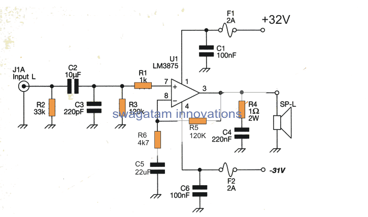
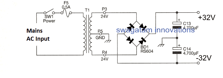
 PA systems are normally employed in different public areas that calls for an human speaker, artist, etc.
to be loudly audible over a substantial distance so that the speech of the person using the PA system becomes audible to a large gathering or crowd.
Common places where a PA system can be used are sports stadiums, public vehicles, and live rock and music venues, and occasions.
A PA system can consist of several microphones or additional audio sources, an audio mixer unit which are able to blend and customize the audio signals coming from the various sources, and amplifiers.
The output is subsequently fed to a loudspeaker for getting an amplified volume, resulting in a wider distribution of the sound.
PA systems are normally employed in different public areas that calls for an human speaker, artist, etc.
to be loudly audible over a substantial distance so that the speech of the person using the PA system becomes audible to a large gathering or crowd.
Common places where a PA system can be used are sports stadiums, public vehicles, and live rock and music venues, and occasions.
A PA system can consist of several microphones or additional audio sources, an audio mixer unit which are able to blend and customize the audio signals coming from the various sources, and amplifiers.
The output is subsequently fed to a loudspeaker for getting an amplified volume, resulting in a wider distribution of the sound.
 The proposed public address circuit explained in this article works with a small speaker, whose impedance is unimportant.
This speaker is hooked up across the emitter of Q1.
The above tiny speaker is used like a microphone, where the user needs to speak for getting his voice amplified.
Q1 is configured in the common base format which causes an extremely increased signal to be generated and fed across its collector.
Transistor Q2, is wired up in the common emitter configuration.
Q2 is used for increasing the amplification further.
The audio or the speech signal from the collector of Q2 is applied by means of the C3 which acts like a blocking capacitor to VR1, configured like a volume control.
The general de-stabilisation is achieved by having the base biasing of Q1 through the emitter of Q2.
The design of this public address power amplifier circuit is reasonably standard and is configured using a robust looking output stage.
This strong output stage is employed so that the amplifier is able to drive a couple of large P.A.
type horns in parallel.
With these types of load at the output we can expect an output power of 8W over the horns or the speakers.
Because the public address or PA amplifier circuit is supposed to be used for amplifying mostly the human speech, a wide bandwidth specification is not important.
Therefore, the capacitor C7 is included to roll off any frequency response that may appear over the 5kHz range.
The capacitor C6 is additionally employed for delivering a fast roll off around the bass frequency region.
Power transistors Q7 and Q9 must be installed with a 5" x 4" finned type heatsink.
Make sure the body of the transistor Q4 remains thermally in contact with the heatsink.
The proposed public address circuit explained in this article works with a small speaker, whose impedance is unimportant.
This speaker is hooked up across the emitter of Q1.
The above tiny speaker is used like a microphone, where the user needs to speak for getting his voice amplified.
Q1 is configured in the common base format which causes an extremely increased signal to be generated and fed across its collector.
Transistor Q2, is wired up in the common emitter configuration.
Q2 is used for increasing the amplification further.
The audio or the speech signal from the collector of Q2 is applied by means of the C3 which acts like a blocking capacitor to VR1, configured like a volume control.
The general de-stabilisation is achieved by having the base biasing of Q1 through the emitter of Q2.
The design of this public address power amplifier circuit is reasonably standard and is configured using a robust looking output stage.
This strong output stage is employed so that the amplifier is able to drive a couple of large P.A.
type horns in parallel.
With these types of load at the output we can expect an output power of 8W over the horns or the speakers.
Because the public address or PA amplifier circuit is supposed to be used for amplifying mostly the human speech, a wide bandwidth specification is not important.
Therefore, the capacitor C7 is included to roll off any frequency response that may appear over the 5kHz range.
The capacitor C6 is additionally employed for delivering a fast roll off around the bass frequency region.
Power transistors Q7 and Q9 must be installed with a 5" x 4" finned type heatsink.
Make sure the body of the transistor Q4 remains thermally in contact with the heatsink.
 In order to determine an A.C.
signal, you have to rotate the volume control to the highest level, and connect the input signal to the socket and start with the switch SW1 positioned to select the minimum sensitivity, until LED just lights up.
The input signal value can be now determined by the position of the switch.
The gain of 1C1 which is a 741 op amp, is fixed through the ratio of the resistive divider formed by R9 and R1 to R6. The resistors R1 to R6 adjust the 741 gain from a level of 20 to 0.5.
Hence, in order to generate 100mV across RV1, the amount of input signal would be around 5mV to 200mV.
Resistors R7 and R8 does the work of biasing the non-inverting input to 4.5V, while the resistor R10 is incorporated to safeguard the IC.
Considering that D.C.
gain of this bench amplifier circuit has the value of unity, the output could be established with +4.5V D.C., enabling highest voltage swing functionality.
In order to decrease the output offset, resulting from the bias current, the value of the parallel resistor R7 and R8 must be roughly identical to the value of the R9. Remember the above point, if you wish you use a different supply voltage for this bench amplifier circuit.
Resistor R11 and capacitor C2 do the work of decoupling the 741 supply lines, just like the capacitor C6 does for the IC LM380. It may be possible to increase the value of capacitor C6 for getting a better DC, if the supply voltage is not regulated and stable.
In order to determine an A.C.
signal, you have to rotate the volume control to the highest level, and connect the input signal to the socket and start with the switch SW1 positioned to select the minimum sensitivity, until LED just lights up.
The input signal value can be now determined by the position of the switch.
The gain of 1C1 which is a 741 op amp, is fixed through the ratio of the resistive divider formed by R9 and R1 to R6. The resistors R1 to R6 adjust the 741 gain from a level of 20 to 0.5.
Hence, in order to generate 100mV across RV1, the amount of input signal would be around 5mV to 200mV.
Resistors R7 and R8 does the work of biasing the non-inverting input to 4.5V, while the resistor R10 is incorporated to safeguard the IC.
Considering that D.C.
gain of this bench amplifier circuit has the value of unity, the output could be established with +4.5V D.C., enabling highest voltage swing functionality.
In order to decrease the output offset, resulting from the bias current, the value of the parallel resistor R7 and R8 must be roughly identical to the value of the R9. Remember the above point, if you wish you use a different supply voltage for this bench amplifier circuit.
Resistor R11 and capacitor C2 do the work of decoupling the 741 supply lines, just like the capacitor C6 does for the IC LM380. It may be possible to increase the value of capacitor C6 for getting a better DC, if the supply voltage is not regulated and stable.

 The IC LM380 is an integrated audio amplifier that, provides a constant gain of 50 (34 dB) and, could be hooked up in either inverting or non -inverting mode (meaning output can be connected in the 'out of phase' manner or 'in phase' with respect to the input signal source).
A pair of of LM380 ICs can be seen wired up in a bridge configuration to enable increased power output using a rather lower power supply voltage of 12 V.
To accomplish this, we operate the two amplifiers using the identical input signal.
However we link the common signal one with the inverting, and the other with the non-inverting modes of the amplifier.
The loudspeaker is then hooked up between the two bridged LM380 amplifier circuits, so that it can consequently get two times more output amplification compared to a single IC.
The input necessary for 100 % power output is approximately 50 millivolts.
Therefore an input attenuator can be seen included in the design to boost the input specification to around 1 volt so that it allows the user with a preset adjustment to accommodate the majority of the signals from radios, USBs, or cellphones.
We can be see a trimpot on the PCB provided for tweaking the sensitivity of the bridged amplifier so that complete volume range becomes available for the volume control of the source signal, with around 50 % rotation of the trimpot.
If it becomes necessary, a separate potentiometer could be employed instead of the preset for the volume control implementation.
The IC's output voltage will be about 50 % of the supply voltage.
Remember that, because the loudspeaker is connected directly, any minor variation in the outputs of the amplifier will cause a dc current to enter into the loudspeaker.
The IC LM380 is an integrated audio amplifier that, provides a constant gain of 50 (34 dB) and, could be hooked up in either inverting or non -inverting mode (meaning output can be connected in the 'out of phase' manner or 'in phase' with respect to the input signal source).
A pair of of LM380 ICs can be seen wired up in a bridge configuration to enable increased power output using a rather lower power supply voltage of 12 V.
To accomplish this, we operate the two amplifiers using the identical input signal.
However we link the common signal one with the inverting, and the other with the non-inverting modes of the amplifier.
The loudspeaker is then hooked up between the two bridged LM380 amplifier circuits, so that it can consequently get two times more output amplification compared to a single IC.
The input necessary for 100 % power output is approximately 50 millivolts.
Therefore an input attenuator can be seen included in the design to boost the input specification to around 1 volt so that it allows the user with a preset adjustment to accommodate the majority of the signals from radios, USBs, or cellphones.
We can be see a trimpot on the PCB provided for tweaking the sensitivity of the bridged amplifier so that complete volume range becomes available for the volume control of the source signal, with around 50 % rotation of the trimpot.
If it becomes necessary, a separate potentiometer could be employed instead of the preset for the volume control implementation.
The IC's output voltage will be about 50 % of the supply voltage.
Remember that, because the loudspeaker is connected directly, any minor variation in the outputs of the amplifier will cause a dc current to enter into the loudspeaker.
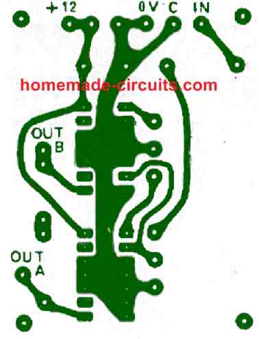
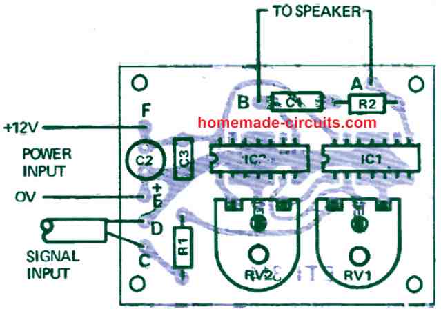 As can be seen in the layout diagram, the a pair of variable resistors or presets are given for setting up the amplifier.
The, RV1 which is for adjusting the volume of the amplifier should be tweaked according to the output voltage available from the music source which is being amplified.
The sensitivity spec of this bridged amplifier circuit will be 5 watts output will be when with RV1 is adjusted at its maximum sensitivity level, with an input signal level of 50 mV.
This input level should be totally sufficient since many radios might deliver higher than 200 millivolts.
The second variable resistors which is for the balance control must be adjusted to get the lowest DC into the speakers as explained in the following paragraphs.
As can be seen in the layout diagram, the a pair of variable resistors or presets are given for setting up the amplifier.
The, RV1 which is for adjusting the volume of the amplifier should be tweaked according to the output voltage available from the music source which is being amplified.
The sensitivity spec of this bridged amplifier circuit will be 5 watts output will be when with RV1 is adjusted at its maximum sensitivity level, with an input signal level of 50 mV.
This input level should be totally sufficient since many radios might deliver higher than 200 millivolts.
The second variable resistors which is for the balance control must be adjusted to get the lowest DC into the speakers as explained in the following paragraphs.
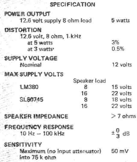
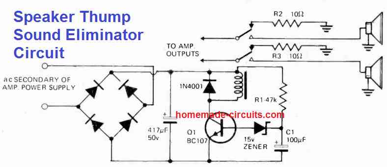 As can be seen in the figure above, the loudspeaker thump sound eliminator circuit is actually built around a delay ON timer circuit.
The transistor Q1 and the relay together with the capacitor C1 provides a delay of about 2 seconds before the relay is switched ON.
The relay can be seen wired with the loudspeakers, the amplifier and 10 ohm resistors.
The power to the transistor relay timer circuit is derived from the amplifier power supply itself.
When power to the amplifier is switched ON, the speaker remains disconnected initially since the relay does not switch ON due to the delay ON timer action.
During this time, the capacitors inside the amplifier quickly charge through the 10 ohm resistor, connected with the N/C contacts of the relay.
Once the initial delay is over, the transistor conducts and powers the relay, which in turn connects the loudspeaker with the amplifier.
The loudspeaker now makes no thumping or popping noise, since the amplifier capacitor are already charged up and the shorting of current to the speakers does not happen.
In this way the thump noise is eliminated from the speakers.
The above working takes care of the amplifier switch ON issue, however when the amplifier is switched OFF, the transistor relay switches OFF quickly, preventing the amplifier capacitors from discharging through the loudspeakers.
Instead, the relay contacts now connect them back to the 10 ohm resistors so that the internal capacitors can now discharge safely through the 10 ohm resistors.
Due to this again the thump sound is eliminated from happening during the power switch OFF.
As can be seen in the figure above, the loudspeaker thump sound eliminator circuit is actually built around a delay ON timer circuit.
The transistor Q1 and the relay together with the capacitor C1 provides a delay of about 2 seconds before the relay is switched ON.
The relay can be seen wired with the loudspeakers, the amplifier and 10 ohm resistors.
The power to the transistor relay timer circuit is derived from the amplifier power supply itself.
When power to the amplifier is switched ON, the speaker remains disconnected initially since the relay does not switch ON due to the delay ON timer action.
During this time, the capacitors inside the amplifier quickly charge through the 10 ohm resistor, connected with the N/C contacts of the relay.
Once the initial delay is over, the transistor conducts and powers the relay, which in turn connects the loudspeaker with the amplifier.
The loudspeaker now makes no thumping or popping noise, since the amplifier capacitor are already charged up and the shorting of current to the speakers does not happen.
In this way the thump noise is eliminated from the speakers.
The above working takes care of the amplifier switch ON issue, however when the amplifier is switched OFF, the transistor relay switches OFF quickly, preventing the amplifier capacitors from discharging through the loudspeakers.
Instead, the relay contacts now connect them back to the 10 ohm resistors so that the internal capacitors can now discharge safely through the 10 ohm resistors.
Due to this again the thump sound is eliminated from happening during the power switch OFF.
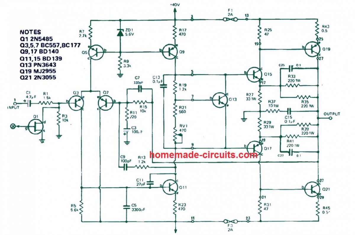 Referring to the circuit diagram above, the music input signal is applied through C1 and R1 to the Q3 base.
Transistor Q3 along with transistor Q7, works like a a differential pair.
Transistor Q5 is configured like a constant current source wherein the current is determined using the formula is 15.6 V (ZD1) - 0.6 (Q5)/2700 (R7), which is approximately equal to 2 mA.
This current is uniformly used among the transistors Q3 and Q7.
Transistor Q9 also serves like a constant current source delivering around 10 mA which, under the absence of an input signal, in driven by means of Q13 and Q11. The differential transistor pair regulates Q11 which in turn controls the voltage at its collector.
The R19 and R21 resistor along with the potentiometer RV1, regulate the voltage across Q13 to approximately 1.9 volts.
However since Q13 is attached to the heatsink, this voltage might fluctuate as the heatsink temperature changes.
Supposing that the voltage on the indicated points 5 and 9 is spread uniformly to around zero volts (ie ¡À 0.95 volts), the current is going to be fixed at approximately 12 mA by means of transistors Q15 and Q17.
The 47 ohm resistors which are R25 and R31, create a voltage drop which becomes sufficient to slightly switch ON the output transistors so that it produces around 100 mA quiescent current.
This quiescent current can be, adjusted and set through the potentiometer RV1.
The resistor R33, R35, R39, R41 are configured and used for applying the local feedback to the output stage.
This provides the output stage with a voltage gain of about four.
The general feedback achieved through the resistor R15, helps the amplifier to get the necessary gain control.
The fuses ensure that the amplifier remain protected from output short circuits and overload conditions.
To achieve good temperature stability Q13 must be attached to a suitably rated heatsink.
Q13 can as a result automatically adapt and regulate bias voltage.
The parts C9/R13, CS, C7, C11, C25 and C27 are used to include sufficient frequency stability for the amplifier.
Referring to the circuit diagram above, the music input signal is applied through C1 and R1 to the Q3 base.
Transistor Q3 along with transistor Q7, works like a a differential pair.
Transistor Q5 is configured like a constant current source wherein the current is determined using the formula is 15.6 V (ZD1) - 0.6 (Q5)/2700 (R7), which is approximately equal to 2 mA.
This current is uniformly used among the transistors Q3 and Q7.
Transistor Q9 also serves like a constant current source delivering around 10 mA which, under the absence of an input signal, in driven by means of Q13 and Q11. The differential transistor pair regulates Q11 which in turn controls the voltage at its collector.
The R19 and R21 resistor along with the potentiometer RV1, regulate the voltage across Q13 to approximately 1.9 volts.
However since Q13 is attached to the heatsink, this voltage might fluctuate as the heatsink temperature changes.
Supposing that the voltage on the indicated points 5 and 9 is spread uniformly to around zero volts (ie ¡À 0.95 volts), the current is going to be fixed at approximately 12 mA by means of transistors Q15 and Q17.
The 47 ohm resistors which are R25 and R31, create a voltage drop which becomes sufficient to slightly switch ON the output transistors so that it produces around 100 mA quiescent current.
This quiescent current can be, adjusted and set through the potentiometer RV1.
The resistor R33, R35, R39, R41 are configured and used for applying the local feedback to the output stage.
This provides the output stage with a voltage gain of about four.
The general feedback achieved through the resistor R15, helps the amplifier to get the necessary gain control.
The fuses ensure that the amplifier remain protected from output short circuits and overload conditions.
To achieve good temperature stability Q13 must be attached to a suitably rated heatsink.
Q13 can as a result automatically adapt and regulate bias voltage.
The parts C9/R13, CS, C7, C11, C25 and C27 are used to include sufficient frequency stability for the amplifier.
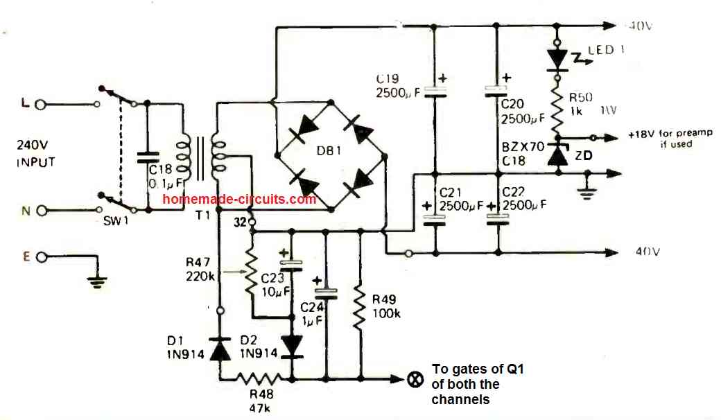 The power supply is actually a standard full-wave bridge having a center tap, which generates a dual supply of + 40 volts and -40 volts and ground voltage for operating the 70 watt stereo amplifier.
Diode D1 does the rectification of a second negative supply which is employed for controlling the Q1 FET for both the channels.
Because of the inclusion of a series resistance with the diode, the capacitor C24 is charged slowly.
Furthermore, while C23 is charged it also adds a slight delay to the power switch ON and switch off.
The power supply is actually a standard full-wave bridge having a center tap, which generates a dual supply of + 40 volts and -40 volts and ground voltage for operating the 70 watt stereo amplifier.
Diode D1 does the rectification of a second negative supply which is employed for controlling the Q1 FET for both the channels.
Because of the inclusion of a series resistance with the diode, the capacitor C24 is charged slowly.
Furthermore, while C23 is charged it also adds a slight delay to the power switch ON and switch off.
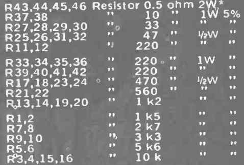
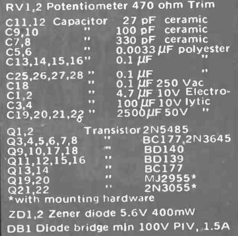
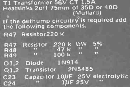
 L1 is roughly tuned to the desired frequency band through T1, to enable the signal input to reach the gate 1 of FET TR1.
TR2 works like the local oscillator, and the functioning frequency in this design is fixed through the inductor L2 and trimmer T2. Oscillator function is implemented via C3 on the gate 2 of FET TR1.
The output frequency from the TR1 drain which forms the mixer stage causes the difference between frequencies of G1 and G2. Therefore when the signal at G1 is 144 MHz, and TR2 is adjusted to oscillate at frequency of 116 MHz, the output is set at 144 MHz - 116 MHz = 28 MHz.
In the same way, when the oscillator is fixed at 116 MHz, supplying an input with 146 MHz to gate G1 provides an output of 30 MHz.
Consequently, 144- 146 MHz could be covered by adjusting the receiver from 28 MHz to 30 MHz.
L3 is approximately adjusted to this band, and L4 connects the signal to the short wave receiver.
The oscillator may basically be adjusted over or under the converter's antenna circuit frequency, since it is the converter's difference between the signal input and oscillator frequencies that decides the output frequency of the converter .
It is additionally feasible to select some other transmission bands and output frequencies, if coils L1, L2 and L3 are apprpriately customized.
L1 is roughly tuned to the desired frequency band through T1, to enable the signal input to reach the gate 1 of FET TR1.
TR2 works like the local oscillator, and the functioning frequency in this design is fixed through the inductor L2 and trimmer T2. Oscillator function is implemented via C3 on the gate 2 of FET TR1.
The output frequency from the TR1 drain which forms the mixer stage causes the difference between frequencies of G1 and G2. Therefore when the signal at G1 is 144 MHz, and TR2 is adjusted to oscillate at frequency of 116 MHz, the output is set at 144 MHz - 116 MHz = 28 MHz.
In the same way, when the oscillator is fixed at 116 MHz, supplying an input with 146 MHz to gate G1 provides an output of 30 MHz.
Consequently, 144- 146 MHz could be covered by adjusting the receiver from 28 MHz to 30 MHz.
L3 is approximately adjusted to this band, and L4 connects the signal to the short wave receiver.
The oscillator may basically be adjusted over or under the converter's antenna circuit frequency, since it is the converter's difference between the signal input and oscillator frequencies that decides the output frequency of the converter .
It is additionally feasible to select some other transmission bands and output frequencies, if coils L1, L2 and L3 are apprpriately customized.
 TR1 can be any RF dual gate FET.
Aerial input is applied to an intermediate tapping on inductor L1, which can be usually through a co-axial feeder.
In a few conditions a small straight aerial or cord could be employed for getting ample signal power.
A raised up antenna may normally improve the reception range.
However, an initial attempt could be to start with a simple dipole antenna design.
This is often of rigid wire, which could be around 38in long overall, with the connecting cable climbing down through the middle.
This kind of antenna may have lower directivlty therefore does not need to be adjusted, and could be elevated over a light-weight post or mast.
For receiving 144-146 MHz signal, L1 is permanently adjusted to approximately 145 MHz by means of T1. Input is applied to gate 1, via a 2nd tapping, and R3 using the by-pass capacitor C2 delivers biasing to the source terminal.
Gate 2 is controlled with a constant voltage extracted through the divider R1/R2. TR1 drain output is attached to the L2 tapping, tuned by trimmer T2.
To get a narrow range of frequencies like the 2 m Amateur band, adjustable tuning cannot be validated, particularly since L1 and L2 never tune finely.
L3 hooks up to any desired 2 m gadget, which may be typically a converter functioning into a lower frequency receiver.
TR1 can be any RF dual gate FET.
Aerial input is applied to an intermediate tapping on inductor L1, which can be usually through a co-axial feeder.
In a few conditions a small straight aerial or cord could be employed for getting ample signal power.
A raised up antenna may normally improve the reception range.
However, an initial attempt could be to start with a simple dipole antenna design.
This is often of rigid wire, which could be around 38in long overall, with the connecting cable climbing down through the middle.
This kind of antenna may have lower directivlty therefore does not need to be adjusted, and could be elevated over a light-weight post or mast.
For receiving 144-146 MHz signal, L1 is permanently adjusted to approximately 145 MHz by means of T1. Input is applied to gate 1, via a 2nd tapping, and R3 using the by-pass capacitor C2 delivers biasing to the source terminal.
Gate 2 is controlled with a constant voltage extracted through the divider R1/R2. TR1 drain output is attached to the L2 tapping, tuned by trimmer T2.
To get a narrow range of frequencies like the 2 m Amateur band, adjustable tuning cannot be validated, particularly since L1 and L2 never tune finely.
L3 hooks up to any desired 2 m gadget, which may be typically a converter functioning into a lower frequency receiver.
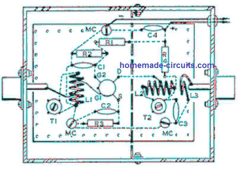
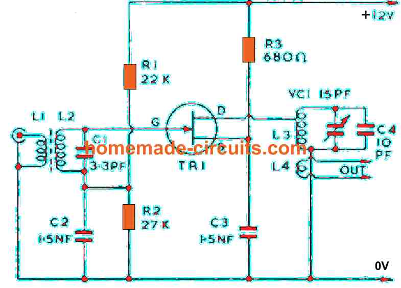 For any wide band reception for example around 88-108 MHz, performance drops down a lot at frequencies away at which the amplifier is tuned.
The circuit in explained below features an adjustable tuning for the drain coil, and in order to minimize unwanted effects, the less significant antenna circuit, which actually tunes flatly, is broad banded.
For any wide band reception for example around 88-108 MHz, performance drops down a lot at frequencies away at which the amplifier is tuned.
The circuit in explained below features an adjustable tuning for the drain coil, and in order to minimize unwanted effects, the less significant antenna circuit, which actually tunes flatly, is broad banded.
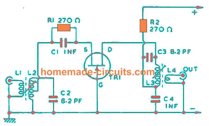 The gain from this design is lower compared to a grounded source stage type design.
The L2 inductor tuning is quite flat.
R1, together with the by-pass capacitor C1, is positioned for biasing the source terminal of the FET, and should be tapped down from the L2 since the input TR1 offers quite a low impedance in this RF circuit.
You are able to get a minor enhancement in results by tapping the down the FET drain via L3.
L2 and L3 are adjusted through their respective screws, which are air cored.
The tuning is optimized by adjusting the cores associated with L2 and L3.
That said, permanent cores designed to suit 70 MHz RF converters, can be also used, and then C2 and C3 could be set up accordingly.
The gain from this design is lower compared to a grounded source stage type design.
The L2 inductor tuning is quite flat.
R1, together with the by-pass capacitor C1, is positioned for biasing the source terminal of the FET, and should be tapped down from the L2 since the input TR1 offers quite a low impedance in this RF circuit.
You are able to get a minor enhancement in results by tapping the down the FET drain via L3.
L2 and L3 are adjusted through their respective screws, which are air cored.
The tuning is optimized by adjusting the cores associated with L2 and L3.
That said, permanent cores designed to suit 70 MHz RF converters, can be also used, and then C2 and C3 could be set up accordingly.
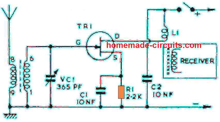 The booster may not be so useful for nearby stations or local channel reception, which doesn't actually matter since this MW booster is not supposed to be permanently installed with the radio receiver anyway.
The boosting range of this circuit is around 1.6 MHz to 550 kHz,
which could be tweaked to match the AM receiver band, simply by altering the position of the coil core.
The booster may not be so useful for nearby stations or local channel reception, which doesn't actually matter since this MW booster is not supposed to be permanently installed with the radio receiver anyway.
The boosting range of this circuit is around 1.6 MHz to 550 kHz,
which could be tweaked to match the AM receiver band, simply by altering the position of the coil core.
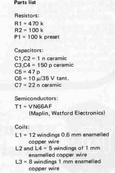 Of course skilled hands may want to play with the coil data, no issues since the suggested RF amplifier is highly adaptable to allow this.
The amplifier is okay for the majority of of transmission primarily since the FET drain current is adjustable via the preset P1.
With regard to linear applications (AM and SSBI, the drain must be fixed at 20 mA.
If intended for FM and CW, P1 must be tweaked to ensure that no quiescent currant is passing through the FET).
If you want to apply for the original purpose, then the quiescent current must be set between 200 mA and 300 mA.
The ready made printed circuit board shown below guarantees fast and precise development.
Of course skilled hands may want to play with the coil data, no issues since the suggested RF amplifier is highly adaptable to allow this.
The amplifier is okay for the majority of of transmission primarily since the FET drain current is adjustable via the preset P1.
With regard to linear applications (AM and SSBI, the drain must be fixed at 20 mA.
If intended for FM and CW, P1 must be tweaked to ensure that no quiescent currant is passing through the FET).
If you want to apply for the original purpose, then the quiescent current must be set between 200 mA and 300 mA.
The ready made printed circuit board shown below guarantees fast and precise development.
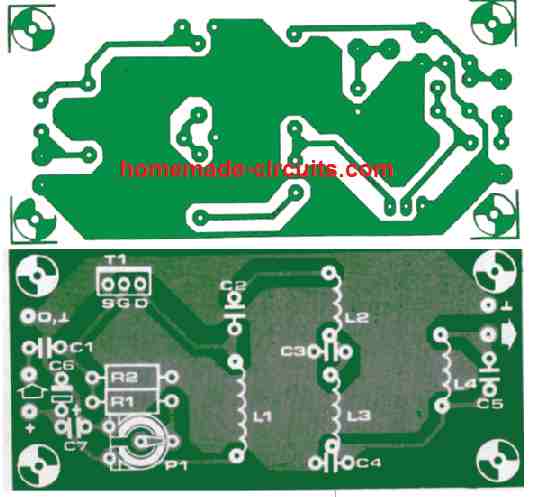 The coils must be wound onto aerial coil formers having 9 mm diameter.
Always be careful that the windings is tightly wound without any spaces.
Make sure you apply a heat sink for the FET.
The coils must be wound onto aerial coil formers having 9 mm diameter.
Always be careful that the windings is tightly wound without any spaces.
Make sure you apply a heat sink for the FET.
 This RF preamplifier is designed for 6-meter frequency band.
Meaning it is suitable for 60 to 70 MHz frequency which are generally used for TV signal transmissions.
Tuning is not required, since the circuit has a broadband 10 MHz range.
This RF preamplifier is designed for 6-meter frequency band.
Meaning it is suitable for 60 to 70 MHz frequency which are generally used for TV signal transmissions.
Tuning is not required, since the circuit has a broadband 10 MHz range.
 The circuit indicated employs a couple of matched up sensors, the 2nd one supplied with a 1kHz sinewave, fine-tuned in amplitude through the error amplifier circuit so that the outputs will be well balanced.
A chopper made up of Four 1N4149 diodes delivers the 1kHz square, that is subsequently shaped into a sinewave through the op amp, and in addition gives a dc level relative to the amplitude.
This is an assessment of the rf input level and is displayed, in this instance, by a moving-coil meter marked in decibels, although this might quickly be made digital.
Ranges of 10dB are determined in the 1kHz drive to include the 55dB dynamic range, and the error integrator capacitors are switched to deliver the appropriate time constant.
The circuit is naturally very linear.
The 10kS2 multi-turn pot is used to set the meter at zero.
Supplemental diodes around the meter overcome reverse polarity in the event the integrator is set too low below zero, because the chopper gives just forward drive for the meter.
On the integrator output, the 4.7k pot is used for setting up the maximum meter current.
Precision to many hundred MHz is approximately 0.1dB, without depending on regulated power supplies.
Capacitors designated C must be of the identical variety to complement temperature coefficients.
The circuit indicated employs a couple of matched up sensors, the 2nd one supplied with a 1kHz sinewave, fine-tuned in amplitude through the error amplifier circuit so that the outputs will be well balanced.
A chopper made up of Four 1N4149 diodes delivers the 1kHz square, that is subsequently shaped into a sinewave through the op amp, and in addition gives a dc level relative to the amplitude.
This is an assessment of the rf input level and is displayed, in this instance, by a moving-coil meter marked in decibels, although this might quickly be made digital.
Ranges of 10dB are determined in the 1kHz drive to include the 55dB dynamic range, and the error integrator capacitors are switched to deliver the appropriate time constant.
The circuit is naturally very linear.
The 10kS2 multi-turn pot is used to set the meter at zero.
Supplemental diodes around the meter overcome reverse polarity in the event the integrator is set too low below zero, because the chopper gives just forward drive for the meter.
On the integrator output, the 4.7k pot is used for setting up the maximum meter current.
Precision to many hundred MHz is approximately 0.1dB, without depending on regulated power supplies.
Capacitors designated C must be of the identical variety to complement temperature coefficients.
 The Broadband RF Amplifier is straightforward, low-cost, and could be constructed totally using junk electronic components.
The only safety measure that you need to take is to ensure that component pin lengths are maintained as small as is possible, and that Mylar type capacitors are employed for the bypass capacitors as pointed out.
The Broadband RF Amplifier is straightforward, low-cost, and could be constructed totally using junk electronic components.
The only safety measure that you need to take is to ensure that component pin lengths are maintained as small as is possible, and that Mylar type capacitors are employed for the bypass capacitors as pointed out.
 The concept is simple: the duty cycle of a rectangular signal of higher frequency is controlled by an input signal.
The switch-on time of the pulse is relative to the instantaneous amplitude of the input signal.
The amount of the on-time and off-time in addition to the frequency is constant.
Therefore, when an input signal is missing, a symmetrical square wave signal is produced.
To achieve relatively good sound quality, the frequency of the rectangular signal must be double than the highest frequency in the input signal.
The resulting signal may be used to power a loudspeaker.
Figure 4 shows a clear conversion in the oscilloscope trace.
The concept is simple: the duty cycle of a rectangular signal of higher frequency is controlled by an input signal.
The switch-on time of the pulse is relative to the instantaneous amplitude of the input signal.
The amount of the on-time and off-time in addition to the frequency is constant.
Therefore, when an input signal is missing, a symmetrical square wave signal is produced.
To achieve relatively good sound quality, the frequency of the rectangular signal must be double than the highest frequency in the input signal.
The resulting signal may be used to power a loudspeaker.
Figure 4 shows a clear conversion in the oscilloscope trace.
 The upper trace shows the output signal post-filtering and measured across the loudspeaker.
The amplitude of the remaining PWM signal that is overlapping the sine wave is small.
The upper trace shows the output signal post-filtering and measured across the loudspeaker.
The amplitude of the remaining PWM signal that is overlapping the sine wave is small.
 Let¡¯s assume when the input is short-circuited, switch Sa powers capacitor C7 with a current I2.
This ensues until a suitable upper limit switching voltage is achieved.
Then, it connects R7 to ground.
After that, C7 is discharged to the lower limit switching voltage of Sa.
As a result, C-7 and R7 produces a square wave with a frequency of 50 kHz.
When an AF signal is effected to the input of the amplifier, the additional current I1 relatively reduces or increases the charge time, or increases and decreases the discharge time.
So, the input signal modifies the duty factor of the square wave signal which is seen at the output of the loudspeaker.
There are two laws which are essential for the basic operation of the PWM amplifier.
The first is switch Sb is controlled in anti-phase with Sa while holding the other loudspeaker terminal as an alternative voltage to that of the PWM signal.
This setup produces an outcome of the switching bridge-type power output stage.
Afterwards, at each polarity, the loudspeaker is forced with the full supply voltage so that a maximum current consumption is achieved.
2. Secondly, we look into inductors L1 and L2.
The purpose of the inductors is to integrate the rectangular signal and convert them into sinusoidal as shown in the scope trace earlier.
Furthermore, they also function and harmonics suppressor of the 50 kHz rectangular signal.
Let¡¯s assume when the input is short-circuited, switch Sa powers capacitor C7 with a current I2.
This ensues until a suitable upper limit switching voltage is achieved.
Then, it connects R7 to ground.
After that, C7 is discharged to the lower limit switching voltage of Sa.
As a result, C-7 and R7 produces a square wave with a frequency of 50 kHz.
When an AF signal is effected to the input of the amplifier, the additional current I1 relatively reduces or increases the charge time, or increases and decreases the discharge time.
So, the input signal modifies the duty factor of the square wave signal which is seen at the output of the loudspeaker.
There are two laws which are essential for the basic operation of the PWM amplifier.
The first is switch Sb is controlled in anti-phase with Sa while holding the other loudspeaker terminal as an alternative voltage to that of the PWM signal.
This setup produces an outcome of the switching bridge-type power output stage.
Afterwards, at each polarity, the loudspeaker is forced with the full supply voltage so that a maximum current consumption is achieved.
2. Secondly, we look into inductors L1 and L2.
The purpose of the inductors is to integrate the rectangular signal and convert them into sinusoidal as shown in the scope trace earlier.
Furthermore, they also function and harmonics suppressor of the 50 kHz rectangular signal.
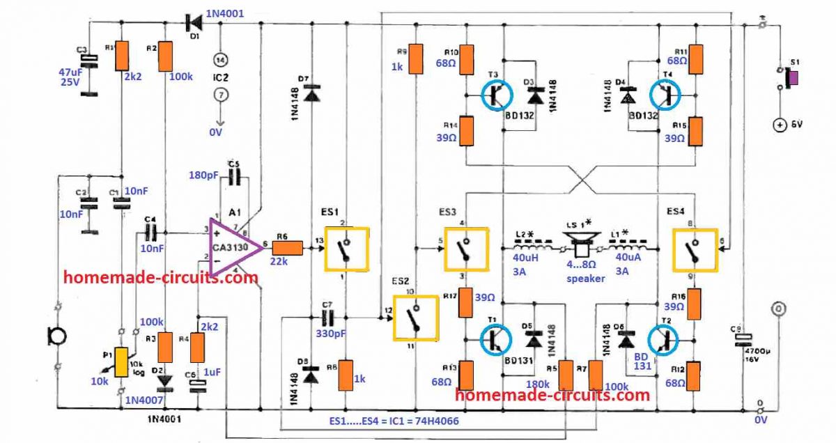 From the schematic in the above figure, you can easily identify the electronic components used in the block diagram.
A handful of parts like resistor R1, coupling capacitors C1 and C4, volume control P1 and an amplifier based around opamp A1 does the biasing job for a capacitor (or electrostatic) microphone.
This whole operation creates the input segment of the PWM amplifier.
As discussed earlier, switches Sa and Sb are built by electronic switches ES1 to ES4 and transistor pairs T1-T3 and T2-T4.
The part indications for the electronic components that construct the PWM generator relate to those described in the block diagram.
Probably the PWM amplifier is uncommonly efficient because the output transistors are not heated up even when forced with an all-drive condition.
In short, there is practically zero dissipation in the power output stage.
The most vital factor you need to consider before selecting inductors L1 and L2 is that they must be able to channel 3 A without becoming saturated.
The actual inductance consideration comes only second.
For example, the inductors used in this project were obtained from a light dimmer.
The purpose of diodes D3 to D6 is to contain the back EMF produced by the inductors to a reasonably safe value.
Moreover, the non-inverting input of opamp A1 is formed by D1, C3, D2 and R3.
This input voltage, efficiently filtered, is equal to half the supply voltage.
When using a traditional opamp amplifier, the voltage gain is assigned by a negative feedback loop.
R4 and R5 will set the gain to 83 to make sure sufficient microphone sensitivity.
In case you¡¯re using high impedance signal sources, R4 can be amplified as needed.
L1 and L2 cause the phase shift and because of that, feedback is possible with the assistance of the square wave signal at the collector of T1 compared to the sinusoidal loudspeaker signal.
Combined with C5 the opamp delivers the significant integration of the PWM feedback signal.
The feedback system lessens the amplifier¡¯s distortion but not so extensively that you might use it for other application besides the public address.
Normally, a significantly increased amount of supply voltage and a complicated circuit design would be required for a Class-D amplifier with low distortion.
Implementing this setup would hamper the overall efficiency of the circuit.
Pay attention when choosing electronic switches in the amplifier as HCMOS types are suitable ones.
A typical CMOS Type 4066 is extremely sluggish and inappropriate to trigger a ¡°short-circuit¡± across T1-T3 and T2-T4.
Not only that, but there is also a heightened risk of overworking or even permanently damaging the amplifier.
From the schematic in the above figure, you can easily identify the electronic components used in the block diagram.
A handful of parts like resistor R1, coupling capacitors C1 and C4, volume control P1 and an amplifier based around opamp A1 does the biasing job for a capacitor (or electrostatic) microphone.
This whole operation creates the input segment of the PWM amplifier.
As discussed earlier, switches Sa and Sb are built by electronic switches ES1 to ES4 and transistor pairs T1-T3 and T2-T4.
The part indications for the electronic components that construct the PWM generator relate to those described in the block diagram.
Probably the PWM amplifier is uncommonly efficient because the output transistors are not heated up even when forced with an all-drive condition.
In short, there is practically zero dissipation in the power output stage.
The most vital factor you need to consider before selecting inductors L1 and L2 is that they must be able to channel 3 A without becoming saturated.
The actual inductance consideration comes only second.
For example, the inductors used in this project were obtained from a light dimmer.
The purpose of diodes D3 to D6 is to contain the back EMF produced by the inductors to a reasonably safe value.
Moreover, the non-inverting input of opamp A1 is formed by D1, C3, D2 and R3.
This input voltage, efficiently filtered, is equal to half the supply voltage.
When using a traditional opamp amplifier, the voltage gain is assigned by a negative feedback loop.
R4 and R5 will set the gain to 83 to make sure sufficient microphone sensitivity.
In case you¡¯re using high impedance signal sources, R4 can be amplified as needed.
L1 and L2 cause the phase shift and because of that, feedback is possible with the assistance of the square wave signal at the collector of T1 compared to the sinusoidal loudspeaker signal.
Combined with C5 the opamp delivers the significant integration of the PWM feedback signal.
The feedback system lessens the amplifier¡¯s distortion but not so extensively that you might use it for other application besides the public address.
Normally, a significantly increased amount of supply voltage and a complicated circuit design would be required for a Class-D amplifier with low distortion.
Implementing this setup would hamper the overall efficiency of the circuit.
Pay attention when choosing electronic switches in the amplifier as HCMOS types are suitable ones.
A typical CMOS Type 4066 is extremely sluggish and inappropriate to trigger a ¡°short-circuit¡± across T1-T3 and T2-T4.
Not only that, but there is also a heightened risk of overworking or even permanently damaging the amplifier.
 Using a 6 V battery pack and a pressure chamber loudspeaker, the amplifier model was easily constructed.
The existing 4 W of output power was measurable in a megaphone with decent audio range.
Four 1.5 V dry batteries or alkaline monocells were connected in series to supply voltage for the megaphone.
In case you want to use this setup frequently, opt for a rechargeable NiCd or gel-type (Dryfit) battery.
Since the maximum current consumption of the megaphone is 0.7 A, a standard alkaline is suitable to support the operation for 24 hours at full output power.
If you plan for non-continuous use, choosing a set of dry cells will be more than enough.
Bear in mind that whatever power source you use, it must never cross more than 7 V.
The reason is the HCMOS switches in IC1 would not function properly at that voltage level or more.
Luckily, for the amplifier, the maximum threshold for supply voltage is larger than 11 V.
PCB design for the above explained PWM class-D amplifier is given below:
Using a 6 V battery pack and a pressure chamber loudspeaker, the amplifier model was easily constructed.
The existing 4 W of output power was measurable in a megaphone with decent audio range.
Four 1.5 V dry batteries or alkaline monocells were connected in series to supply voltage for the megaphone.
In case you want to use this setup frequently, opt for a rechargeable NiCd or gel-type (Dryfit) battery.
Since the maximum current consumption of the megaphone is 0.7 A, a standard alkaline is suitable to support the operation for 24 hours at full output power.
If you plan for non-continuous use, choosing a set of dry cells will be more than enough.
Bear in mind that whatever power source you use, it must never cross more than 7 V.
The reason is the HCMOS switches in IC1 would not function properly at that voltage level or more.
Luckily, for the amplifier, the maximum threshold for supply voltage is larger than 11 V.
PCB design for the above explained PWM class-D amplifier is given below:
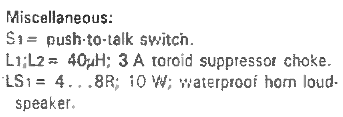
 The input audio signal is applied to an op-amp IC1 which functions as a comparator.
This setup leads a handful of Schmitt triggers which are connected in parallel to the circuit.
They are there for two reasons.
Firstly, there must a ¡°square¡± waveform and secondly, the adequate base drive current is required for the output stage.
In this stage, there are two simple yet fast transistors (BD137/138) installed.
The whole amplifier oscillates and generates a square wave.
The reason is one input from the comparator (IC1) is attached to the output through an RC network.
Furthermore, both inputs of IC1 are biased to the first half of the supply voltage by employing a voltage divider R3/R4.
Each time the IC1¡¯s output is low and the emitters of T1/T2 are high, charging of capacitor C3 occurs through resistor R7. At the same time, there will be a rise in voltage at the non-inverting input.
Once this escalating voltage crosses the level of inverting put, the out of IC1 swaps from low to high.
Resultantly, the emitters of T1/T2 turn from high to low.
This condition allows C3 to discharge through R7 and the voltage at the plus input dips below the voltage at the minus input.
The output of IC1 also reverts to a low state.
In the end, a square wave output is produced at a frequency decided by R7 and C3. The provided values generate an oscillation at 700 kHz.
Using an oscillator, we can modulate the frequency.
The inverting input¡¯s level of IC1 which usually is used as a reference does not stay constant but is decided by the audio signal.
Furthermore, the amplitude determines the exact point where the output of the comparator begins to change.
Consequently, the ¡°thickness¡± of the square waves is regularly modulated by the audio signal.
To ensure the amplifier does not operate as a 700 kHz transmitter, filtering must be exercised at its output.
An LC/RC network comprising L1/C6 and C7/ R6 does a good job as a filter.
The input audio signal is applied to an op-amp IC1 which functions as a comparator.
This setup leads a handful of Schmitt triggers which are connected in parallel to the circuit.
They are there for two reasons.
Firstly, there must a ¡°square¡± waveform and secondly, the adequate base drive current is required for the output stage.
In this stage, there are two simple yet fast transistors (BD137/138) installed.
The whole amplifier oscillates and generates a square wave.
The reason is one input from the comparator (IC1) is attached to the output through an RC network.
Furthermore, both inputs of IC1 are biased to the first half of the supply voltage by employing a voltage divider R3/R4.
Each time the IC1¡¯s output is low and the emitters of T1/T2 are high, charging of capacitor C3 occurs through resistor R7. At the same time, there will be a rise in voltage at the non-inverting input.
Once this escalating voltage crosses the level of inverting put, the out of IC1 swaps from low to high.
Resultantly, the emitters of T1/T2 turn from high to low.
This condition allows C3 to discharge through R7 and the voltage at the plus input dips below the voltage at the minus input.
The output of IC1 also reverts to a low state.
In the end, a square wave output is produced at a frequency decided by R7 and C3. The provided values generate an oscillation at 700 kHz.
Using an oscillator, we can modulate the frequency.
The inverting input¡¯s level of IC1 which usually is used as a reference does not stay constant but is decided by the audio signal.
Furthermore, the amplitude determines the exact point where the output of the comparator begins to change.
Consequently, the ¡°thickness¡± of the square waves is regularly modulated by the audio signal.
To ensure the amplifier does not operate as a 700 kHz transmitter, filtering must be exercised at its output.
An LC/RC network comprising L1/C6 and C7/ R6 does a good job as a filter.
 Parts List
Resistors:
R1 - 22k
R2, R7 - 1M
R3, R4 - 2.2k
R6 - 420 k
R6 - 8.2 Ohms
P1 = 100k logarithmic Potentiometer
Conacitor:
C1,C2 - 100 nF
C3 - 100 pF
C4, C5 - 100¦ÌF/16 V
C6 =68 nF
C7 - 470nF
C8 - 1000p/10 V
C9 - 2n2
Semiconductors:
IC1 - CA3130
IC2- 00106
T1 =BD137
T2 - BD138
Miscellaneous:
L1 =39¦ÌH Inductor
Parts List
Resistors:
R1 - 22k
R2, R7 - 1M
R3, R4 - 2.2k
R6 - 420 k
R6 - 8.2 Ohms
P1 = 100k logarithmic Potentiometer
Conacitor:
C1,C2 - 100 nF
C3 - 100 pF
C4, C5 - 100¦ÌF/16 V
C6 =68 nF
C7 - 470nF
C8 - 1000p/10 V
C9 - 2n2
Semiconductors:
IC1 - CA3130
IC2- 00106
T1 =BD137
T2 - BD138
Miscellaneous:
L1 =39¦ÌH Inductor
 There are only two scenarios ¨C full on or completely off.
Due to that, the dissipation is incredibly small and consequently yields high efficiency.
The output waveform does not look like the input.
However, the integral of the output and input waveforms are proportional to each other relative to time.
The presented table of component values shows that any amplifier with outputs between 3 W to 100 W can be fabricated.
Given that, stronger powers up to 1 kW can be attained.
The disadvantage is that it creates around 30% of distortion.
As a result, the amplifier can be utilised for sound amplifying only.
It is fit for public address systems due to the speech being incredibly understandable.
There are only two scenarios ¨C full on or completely off.
Due to that, the dissipation is incredibly small and consequently yields high efficiency.
The output waveform does not look like the input.
However, the integral of the output and input waveforms are proportional to each other relative to time.
The presented table of component values shows that any amplifier with outputs between 3 W to 100 W can be fabricated.
Given that, stronger powers up to 1 kW can be attained.
The disadvantage is that it creates around 30% of distortion.
As a result, the amplifier can be utilised for sound amplifying only.
It is fit for public address systems due to the speech being incredibly understandable.
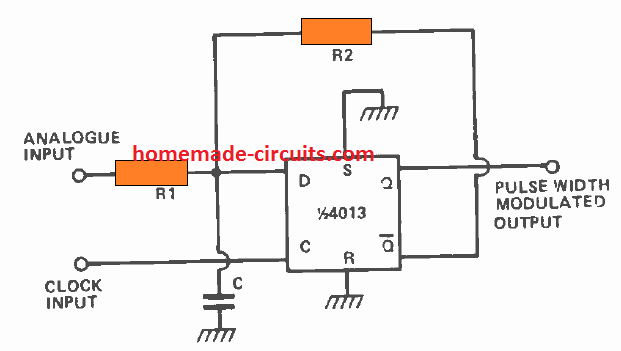 You have to follow the clock pulses as specified and these must be significantly higher in frequency than the desired bandwidth.
The gain is R1/R2 whereas the time R1R2C /(R1 + R2) must be lengthier than the clock pulses¡¯ period.
You have to follow the clock pulses as specified and these must be significantly higher in frequency than the desired bandwidth.
The gain is R1/R2 whereas the time R1R2C /(R1 + R2) must be lengthier than the clock pulses¡¯ period.
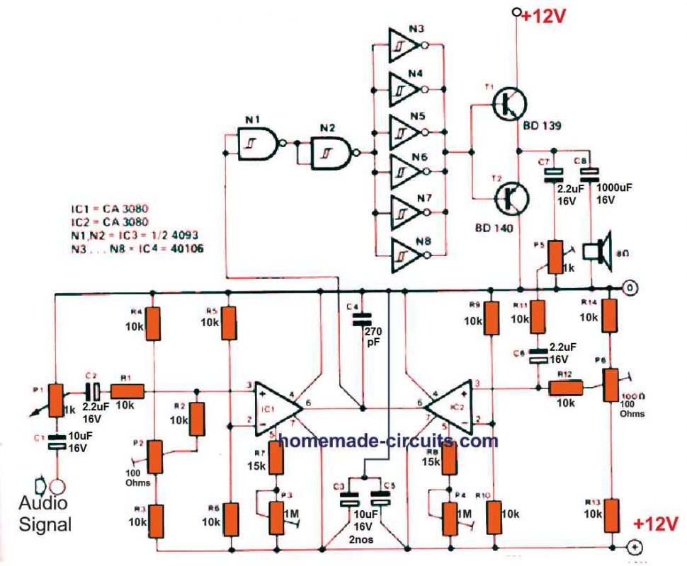 N3 to N8 gates form the comparator, while the two push pull amplifiers form the amplifiers.
The buffer inverter N3---N8 gates are connected in parallel to enable greater amplification of the signal from this stage.
N3 to N8 gates form the comparator, while the two push pull amplifiers form the amplifiers.
The buffer inverter N3---N8 gates are connected in parallel to enable greater amplification of the signal from this stage.
 Here is a workaround that will generate the reverberating bass at tremendous levels.
When compared with other high audio frequencies, the bass is non-directional and therefore does not demand specific speaker positions.
The bass booster speaker system in this post describes how to construct such a circuit without affecting the stereo output or sound quality.
Here is a workaround that will generate the reverberating bass at tremendous levels.
When compared with other high audio frequencies, the bass is non-directional and therefore does not demand specific speaker positions.
The bass booster speaker system in this post describes how to construct such a circuit without affecting the stereo output or sound quality.
 Another alternative is when the above low pass configuration is implemented with the self contained speaker system that is purposefully designed for bass reproduction as discussed in this article.
Since a spare amplifier may be cumbersome, a simple built-in amplifier as the one used in this project was designed.
Another alternative is when the above low pass configuration is implemented with the self contained speaker system that is purposefully designed for bass reproduction as discussed in this article.
Since a spare amplifier may be cumbersome, a simple built-in amplifier as the one used in this project was designed.
 Figure#5
The main power transformer, output transistors and regulation potentiometer are installed externally.
Then, connections are established to and from the components based on the numbers on the PCB layout plan and the schematic.
It must be ensured that all the electronic components are placed according to their correct polarity before soldering.
Transistors Q6 and Q7 are fixed on the heatsink with insulating washers and connected to pins 1, 2, 3, 4 and 5. The connection points are depicted in Figures 2 and 5.
The power transformer must be attached on rubber if the amplifier will be placed inside the speaker enclosure.
Using a shielded cable is advised for making the connection to the inputs and the volume control.
Figure#5
The main power transformer, output transistors and regulation potentiometer are installed externally.
Then, connections are established to and from the components based on the numbers on the PCB layout plan and the schematic.
It must be ensured that all the electronic components are placed according to their correct polarity before soldering.
Transistors Q6 and Q7 are fixed on the heatsink with insulating washers and connected to pins 1, 2, 3, 4 and 5. The connection points are depicted in Figures 2 and 5.
The power transformer must be attached on rubber if the amplifier will be placed inside the speaker enclosure.
Using a shielded cable is advised for making the connection to the inputs and the volume control.
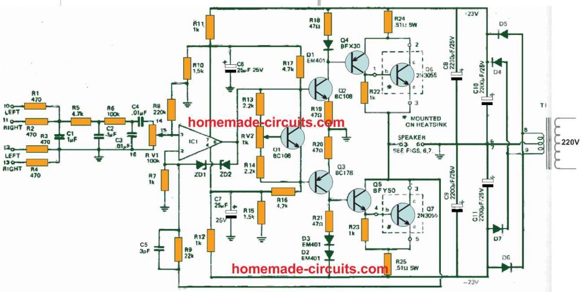 <<FIGURE#2 Self contained high bass, sub-woofer speaker system (transistors/diodes are not critical, any standard equivalent can be used.)>>
Resistors R1 to R4 combine the output from every channel of the present stereo amplifier.
Then, resistors R5, R6 and RV1, in addition to capacitors C1, C2 and C3 create a low-pass filter with a cut-off frequency of about 200Hz.
Moreover, it also has 18 dB per octave slope.
To protect the speakers from switch ON spikes and transients, capacitor C4 functions as a high pass filter with roughly 30 Hz.
Figure 1 displays the filter that is intended for use with different amplifiers has a 20 dB attenuator attached before the output potentiometer.
This guards the subsequent amplifier against overloading.
The amplifier in Figure 2 has a voltage gain of 23
<<FIGURE#2 Self contained high bass, sub-woofer speaker system (transistors/diodes are not critical, any standard equivalent can be used.)>>
Resistors R1 to R4 combine the output from every channel of the present stereo amplifier.
Then, resistors R5, R6 and RV1, in addition to capacitors C1, C2 and C3 create a low-pass filter with a cut-off frequency of about 200Hz.
Moreover, it also has 18 dB per octave slope.
To protect the speakers from switch ON spikes and transients, capacitor C4 functions as a high pass filter with roughly 30 Hz.
Figure 1 displays the filter that is intended for use with different amplifiers has a 20 dB attenuator attached before the output potentiometer.
This guards the subsequent amplifier against overloading.
The amplifier in Figure 2 has a voltage gain of 23 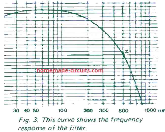 The principal voltage gain of the amplifier circuit is supplied by IC1, Q2 and Q3.
Transistors Q4 and Q5 supply the required current gain to trigger the output transistors Q6 and Q7.
While Q1 stabilizes Q2 and Q3, D1 balances transistor Q4. Then, diodes D3 and D4 compensate transistors Q5 and Q7.
By means of restricting the output voltage swing of the IC, Zener diodes ZD1 and ZD2 protect transistors Q2 and Q3.
There is a possibility to use the amplifier discussed in this assignment without incorporating the filter.
This means the electronic component will act as a direct 40 W mono amplifier.
If that is the case, one of the diodes, D2 or D3 or both must be relocated on the heatsink.
The principal voltage gain of the amplifier circuit is supplied by IC1, Q2 and Q3.
Transistors Q4 and Q5 supply the required current gain to trigger the output transistors Q6 and Q7.
While Q1 stabilizes Q2 and Q3, D1 balances transistor Q4. Then, diodes D3 and D4 compensate transistors Q5 and Q7.
By means of restricting the output voltage swing of the IC, Zener diodes ZD1 and ZD2 protect transistors Q2 and Q3.
There is a possibility to use the amplifier discussed in this assignment without incorporating the filter.
This means the electronic component will act as a direct 40 W mono amplifier.
If that is the case, one of the diodes, D2 or D3 or both must be relocated on the heatsink.

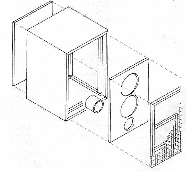 Figure#7
The selected speakers for the bass booster circuit were 2nos 8-ohm Magnavox type 20 W that is parallelly connected.
Therefore, the speakers will only have an impedance of 4 ohms.
The speaker enclosure¡¯s internal was covered with absorptive material like foam, on the sides, top and back surfaces.
Speaker wire connection diagram
Figure#7
The selected speakers for the bass booster circuit were 2nos 8-ohm Magnavox type 20 W that is parallelly connected.
Therefore, the speakers will only have an impedance of 4 ohms.
The speaker enclosure¡¯s internal was covered with absorptive material like foam, on the sides, top and back surfaces.
Speaker wire connection diagram
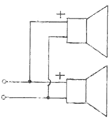
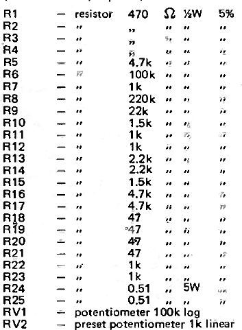 Capacitors:
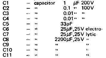 Semiconductors and Miscellaneous
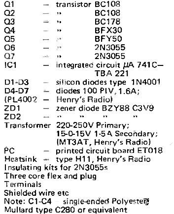
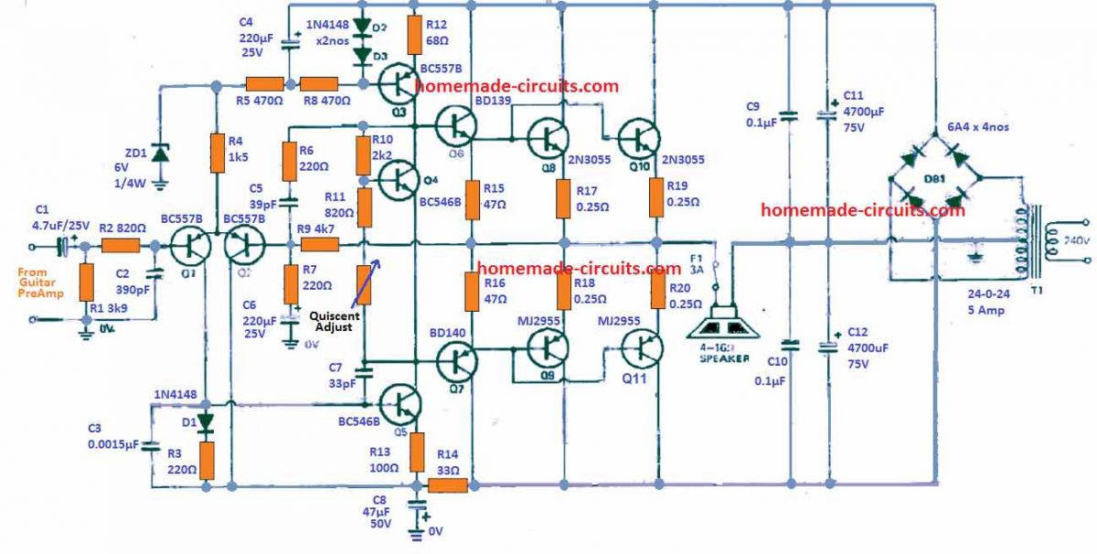 Referring to the above schematic, the guitar power amplifier amplifier employs a quasi-complimentary symmetry, output phase and a differential input phase.
Parallel output transistors are used for an enhanced output capacity while transistors Q6 and Q7 connected in Darlington pair deliver a current gain.
Around 10 mA is provided by the current regulator Q3. This controlled current channels through Q4 and activates the bias for the output stage, and Q5.
The collector voltage at Q5 is determined by its base-emitter voltage.
An extremely high voltage gain is present in this transistor because it is operating almost at constant current.
This high gain is attenuated at large frequencies by capacitor C7.
The differential pair Q1 and Q2 controls transistor Q5. As a result of the negative feedback through R7 and R9, Q1 and Q2 function like an error amplifier.
So, it attempts to retain the voltage at its two inputs at the bases of Q1 and Q2 constant.
Therefore, the output voltage is made equal to the input voltage multiplied by (R9+R7)/R7. Resultantly, the amplifier will have a voltage gain of around 22. Changing the value of R7 will allow the voltage gain to vary.
An apt adjustment must also be made to C6 because R7/C6 regulate the lower -3dB point.
You must ensure to not change the value of R9.
Referring to the above schematic, the guitar power amplifier amplifier employs a quasi-complimentary symmetry, output phase and a differential input phase.
Parallel output transistors are used for an enhanced output capacity while transistors Q6 and Q7 connected in Darlington pair deliver a current gain.
Around 10 mA is provided by the current regulator Q3. This controlled current channels through Q4 and activates the bias for the output stage, and Q5.
The collector voltage at Q5 is determined by its base-emitter voltage.
An extremely high voltage gain is present in this transistor because it is operating almost at constant current.
This high gain is attenuated at large frequencies by capacitor C7.
The differential pair Q1 and Q2 controls transistor Q5. As a result of the negative feedback through R7 and R9, Q1 and Q2 function like an error amplifier.
So, it attempts to retain the voltage at its two inputs at the bases of Q1 and Q2 constant.
Therefore, the output voltage is made equal to the input voltage multiplied by (R9+R7)/R7. Resultantly, the amplifier will have a voltage gain of around 22. Changing the value of R7 will allow the voltage gain to vary.
An apt adjustment must also be made to C6 because R7/C6 regulate the lower -3dB point.
You must ensure to not change the value of R9.
 Ensure that all capacitors, diodes and transistors are correctly placed.
On Q3 and Q5, metal ¡°fin¡± type of heatsinks are utilized.
Double-check that the heatsink has enough space between the other parts.
Another heatsink that is insulated by mica washers is mounted between Q6 and Q7.
Keep in mind that the heatsink will be a little slanted and the transistor somewhat curved.
This is to give space for fastening the heatsink to the ¡°metal side¡± of the transistors.
Always make sure that insulating washers are installed.
The PCB for this guitar amplifier circuit should be fitted against the lid of the metal box and short connecting leads should be connected between the boards to the transistors¡¯ outputs which are plugged on the flip side of this lid.
To make sure the PCB does not touch with the inner face of the lid, countersunk screws and washers are utilized.
It is fundamental to install the fasteners at this stage but avoid fixing the board altogether.
Using the countersunk screw and insulating spacers, the heatsink for Q4 must be secured to the lid.
The heatsinks for the output transistors must be installed now, and ensure the transistors are in their right locations.
Remember to include the insulating washers.
The short leads must be connected to the emitter, base and collector of the output transistors.
This connection to the collectors is done using the transistor mounting screw.
Next, firmly attach transistor Q4 into its heatsink.
In the PCB, place the metal joining pins for terminating connections to the output transistors Q8, Q9, Q10 and Q11. The positions of the pin are visibly etched on the PCB overlay.
After that, plug all the leads from the power supply into the PCB.
Then, fix the board on top of the leads from the output transistors and fasten them tightly.
Solder the leads from the diverse external connections to the selected pins on the board.
Try not to turn the wire around the pins by more than half a turn.
Else, when you need to detach it (for some reasons), it will be tough.
Finally, assemble all remaining parts.
Ensure the mains earth lead is firmly fixed to the case as it acts as a transformer shield too.
The input shield must be earthed to the case directly at the input socket.
Ensure that all capacitors, diodes and transistors are correctly placed.
On Q3 and Q5, metal ¡°fin¡± type of heatsinks are utilized.
Double-check that the heatsink has enough space between the other parts.
Another heatsink that is insulated by mica washers is mounted between Q6 and Q7.
Keep in mind that the heatsink will be a little slanted and the transistor somewhat curved.
This is to give space for fastening the heatsink to the ¡°metal side¡± of the transistors.
Always make sure that insulating washers are installed.
The PCB for this guitar amplifier circuit should be fitted against the lid of the metal box and short connecting leads should be connected between the boards to the transistors¡¯ outputs which are plugged on the flip side of this lid.
To make sure the PCB does not touch with the inner face of the lid, countersunk screws and washers are utilized.
It is fundamental to install the fasteners at this stage but avoid fixing the board altogether.
Using the countersunk screw and insulating spacers, the heatsink for Q4 must be secured to the lid.
The heatsinks for the output transistors must be installed now, and ensure the transistors are in their right locations.
Remember to include the insulating washers.
The short leads must be connected to the emitter, base and collector of the output transistors.
This connection to the collectors is done using the transistor mounting screw.
Next, firmly attach transistor Q4 into its heatsink.
In the PCB, place the metal joining pins for terminating connections to the output transistors Q8, Q9, Q10 and Q11. The positions of the pin are visibly etched on the PCB overlay.
After that, plug all the leads from the power supply into the PCB.
Then, fix the board on top of the leads from the output transistors and fasten them tightly.
Solder the leads from the diverse external connections to the selected pins on the board.
Try not to turn the wire around the pins by more than half a turn.
Else, when you need to detach it (for some reasons), it will be tough.
Finally, assemble all remaining parts.
Ensure the mains earth lead is firmly fixed to the case as it acts as a transformer shield too.
The input shield must be earthed to the case directly at the input socket.
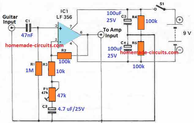 Just one LF 356 delivers the required amplification, that is determined by the ratio of R2 + R3 + P1 to R3 + P1. The input impedance, which, at 1 M, may be pretty high, is specified by R1 since the op -amp includes FET inputs.
This can be a appropriate impedance for the majority of guitar pick-ups.
A 9 V battery supplies the power supply which is transformed into a balanced +/ -4.5 V for the op-amp through R4, R5, C3, and C4.
Current draw of this guitar preamplifier will be approximately 5 mA.
The design including battery could simply be installed inside a tiny enclosure.
If a plug/socket connectors are fitted on the cabinet, the preamp can easily be hooked up into the guitar.
If this is executed, preset P1 could be substituted with any standard potentiometer to facilitate quick amplification control using the pot knob protruding from the case.
Just one LF 356 delivers the required amplification, that is determined by the ratio of R2 + R3 + P1 to R3 + P1. The input impedance, which, at 1 M, may be pretty high, is specified by R1 since the op -amp includes FET inputs.
This can be a appropriate impedance for the majority of guitar pick-ups.
A 9 V battery supplies the power supply which is transformed into a balanced +/ -4.5 V for the op-amp through R4, R5, C3, and C4.
Current draw of this guitar preamplifier will be approximately 5 mA.
The design including battery could simply be installed inside a tiny enclosure.
If a plug/socket connectors are fitted on the cabinet, the preamp can easily be hooked up into the guitar.
If this is executed, preset P1 could be substituted with any standard potentiometer to facilitate quick amplification control using the pot knob protruding from the case.
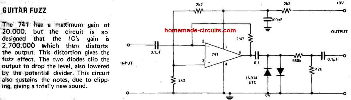
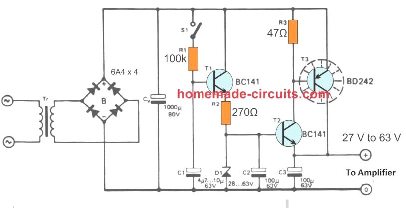 The crude supply is supplied by rectifier B and smoothing capacitor CO.
Zener diode D1 offers the reference voltage, since the output voltage is lower, at around 600 mV.
If it is essential, the intended voltage could be built applying a couple of series connected zeners diodes.
The overall zener voltage could be selected in between 28 V and 63 V (approximately).
Switch S1 toggles the supply on and off (connected to the mains AC switch).
Whenever it is closed or powered ON, the voltage across C1 goes up in around One second upto its working threshold.
The output voltage begins climbing in accordance with the rising voltage across C1 until the level where the zener diode becomes conductive or the firing threshold of the zener.
When S1 is not closed, or is open, the C1 voltage begins dropping down within approximately Five seconds, caused by the leakage through the base current feed for the transistor T1. In case the amplifier exhibits no significant switch-off voltage spikes, so that no specific turn-off procedure is necessary, it may be possible to totally eliminate the switch S1, and connect the S1 points with a wire link..
The unregulated voltage at C1 must not go beyond 80 V.
It must be selected to ensure that there is sufficient voltage drop over T3 to deal with regulation specifications.
Way too high a drop would be a waste of power and even an unnecessary involvement of pricey heat sink.
The basic theory is that, with the supply input fully loaded and the inbound mains AC voltage at its minimum (anticipated) range, there should be approximately 2 volts over the series transistors on the troughs in the ripple waveform.
Alternatively, an acceptable rule of thumb, would be to allow for around 10 volts over T3 (without any load), and expect T3 will, under all circumstances require a minimal heat sink (e.g.
2 mm thick shiny aluminum, about 10 cm by 10 cm).
In severe conditions this might be furthermore essential to enhance T2 with a cooling fins or extensions.
The value of 1000 ¦ÌF capacitor presented for Cv is merely indicated as a representation.
If you would be interested to precisely design the basic transformer/bridge supply also, coupled to a compatible optimum load, that could be easily calculated through the formula Q = CV (keeping in mind that the rectifier produces one hundred ripples every second.
The crude supply is supplied by rectifier B and smoothing capacitor CO.
Zener diode D1 offers the reference voltage, since the output voltage is lower, at around 600 mV.
If it is essential, the intended voltage could be built applying a couple of series connected zeners diodes.
The overall zener voltage could be selected in between 28 V and 63 V (approximately).
Switch S1 toggles the supply on and off (connected to the mains AC switch).
Whenever it is closed or powered ON, the voltage across C1 goes up in around One second upto its working threshold.
The output voltage begins climbing in accordance with the rising voltage across C1 until the level where the zener diode becomes conductive or the firing threshold of the zener.
When S1 is not closed, or is open, the C1 voltage begins dropping down within approximately Five seconds, caused by the leakage through the base current feed for the transistor T1. In case the amplifier exhibits no significant switch-off voltage spikes, so that no specific turn-off procedure is necessary, it may be possible to totally eliminate the switch S1, and connect the S1 points with a wire link..
The unregulated voltage at C1 must not go beyond 80 V.
It must be selected to ensure that there is sufficient voltage drop over T3 to deal with regulation specifications.
Way too high a drop would be a waste of power and even an unnecessary involvement of pricey heat sink.
The basic theory is that, with the supply input fully loaded and the inbound mains AC voltage at its minimum (anticipated) range, there should be approximately 2 volts over the series transistors on the troughs in the ripple waveform.
Alternatively, an acceptable rule of thumb, would be to allow for around 10 volts over T3 (without any load), and expect T3 will, under all circumstances require a minimal heat sink (e.g.
2 mm thick shiny aluminum, about 10 cm by 10 cm).
In severe conditions this might be furthermore essential to enhance T2 with a cooling fins or extensions.
The value of 1000 ¦ÌF capacitor presented for Cv is merely indicated as a representation.
If you would be interested to precisely design the basic transformer/bridge supply also, coupled to a compatible optimum load, that could be easily calculated through the formula Q = CV (keeping in mind that the rectifier produces one hundred ripples every second.
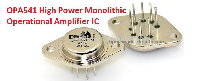
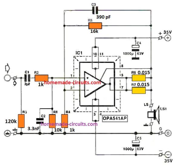 The schematic discussed in this article will deliver approximately 60 watts to 160 watts into an 4 Ohm load.
This is accomplished through a a symmetrical supply voltage of ¡À40 V.
The in-built current limiter of the chip is fixed to an switch ON threshold of around 8.5 A through parallel linked resistors R6/R7.
The schematic discussed in this article will deliver approximately 60 watts to 160 watts into an 4 Ohm load.
This is accomplished through a a symmetrical supply voltage of ¡À40 V.
The in-built current limiter of the chip is fixed to an switch ON threshold of around 8.5 A through parallel linked resistors R6/R7.
 DATASHEET
 This small amplifier is moderately sensitive and can provide 100 % output having an input of approximately 50 mV.
Input impedance is approximately 50k.
A basic tone control is integrated.
Although this is not actually an active tone control, rather than a passive one, the effect is fairly adequate.
The volume control center arm is attached to the Q1 base through a DC blocking capacitor.
This small amplifier is moderately sensitive and can provide 100 % output having an input of approximately 50 mV.
Input impedance is approximately 50k.
A basic tone control is integrated.
Although this is not actually an active tone control, rather than a passive one, the effect is fairly adequate.
The volume control center arm is attached to the Q1 base through a DC blocking capacitor.
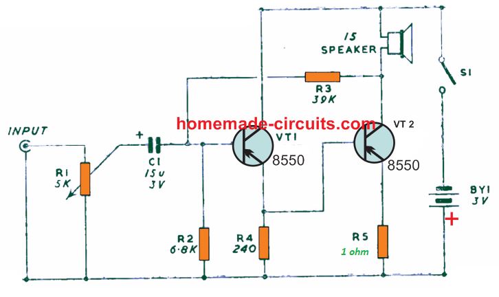 Portion of the standing collector current of Tr1 likewise runs via Tr2 through base to emitter thus delivering the essential bias.
Negative feedback is supplied by R5 and R3. R3 delivers feedback through the two stages and R5 implements feedback through the output to the input of Tr2.
The effect of this feedback results in an incredibly flat response curve down to surprisingly low frequencies.
The high frequency response could be substantially enhanced by changing the transistors with 2N2907. Applying this device may also bring about an boost in gain.
The sub-miniature amplifier circuit may be fantastic for boosting the output from your FM or AM tuner.
In case you have a compact radio, that works only with an earpiece output, it could be accustomed to raise the volume approximately to loudspeaker level.
To get this done just hook up the output from your radio on the input of the amplifier.
The loudspeaker, utilized on this amplifier, must be as big as it can be, if at all possible a 12 inch type inside an housing.
Implementing an extremely small speaker can lead to a bit of inefficiency due to the fact that there could be ample current moving over the winding even while the input signal is not available.
The current utilized through the battery is going to be relatively high, approximately 150 ma.
which means this must be as large as may be possible.
Portion of the standing collector current of Tr1 likewise runs via Tr2 through base to emitter thus delivering the essential bias.
Negative feedback is supplied by R5 and R3. R3 delivers feedback through the two stages and R5 implements feedback through the output to the input of Tr2.
The effect of this feedback results in an incredibly flat response curve down to surprisingly low frequencies.
The high frequency response could be substantially enhanced by changing the transistors with 2N2907. Applying this device may also bring about an boost in gain.
The sub-miniature amplifier circuit may be fantastic for boosting the output from your FM or AM tuner.
In case you have a compact radio, that works only with an earpiece output, it could be accustomed to raise the volume approximately to loudspeaker level.
To get this done just hook up the output from your radio on the input of the amplifier.
The loudspeaker, utilized on this amplifier, must be as big as it can be, if at all possible a 12 inch type inside an housing.
Implementing an extremely small speaker can lead to a bit of inefficiency due to the fact that there could be ample current moving over the winding even while the input signal is not available.
The current utilized through the battery is going to be relatively high, approximately 150 ma.
which means this must be as large as may be possible.
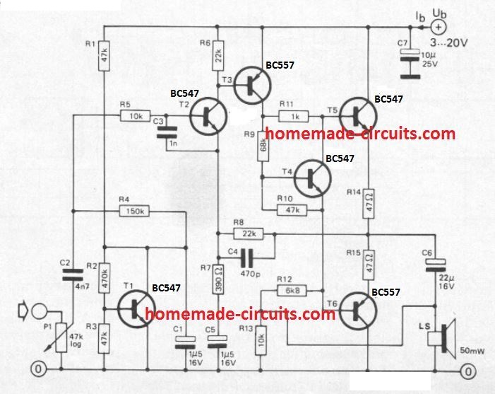 This mini amplifier can work without any issues or errors through supply voltages between 3 V and 20 V using source resistances as:
Supply voltage / 2 mA (k ohms)
The power output that the amplifier could deliver is, naturally, determined by the supply voltage and its loudspeaker resistance, as is visible through the enclosed table.
This mini amplifier can work without any issues or errors through supply voltages between 3 V and 20 V using source resistances as:
Supply voltage / 2 mA (k ohms)
The power output that the amplifier could deliver is, naturally, determined by the supply voltage and its loudspeaker resistance, as is visible through the enclosed table.
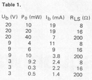 The quiescent current usage of the amplifier is in between 1 mA and 1.5 mA, the precise magnitude dependent on the variety of transistors employed.
If the quiescent current drops beyond this particular limit it will likely be essential to tweak the value of R9. As is evident in the table, the amplifier functions efficiently with high impedance loudspeakers.
Since speakers with impedances as large as 200 ohms cannot be easily available, the choice is to try using a lesser impedance speaker having a complementing transformer.
For instance an 8 ohm speaker may be employed with a transformer using a ratio of around 5:1.
Although the amplifier output power is not very high, it is however adequate enough when combined with a moderately efficient loudspeaker inside a silent area.
The amplifier's voltage gain is around 50 and the 3 dB bandwidth is around 300 Hz to 6 kHz.
The quiescent current usage of the amplifier is in between 1 mA and 1.5 mA, the precise magnitude dependent on the variety of transistors employed.
If the quiescent current drops beyond this particular limit it will likely be essential to tweak the value of R9. As is evident in the table, the amplifier functions efficiently with high impedance loudspeakers.
Since speakers with impedances as large as 200 ohms cannot be easily available, the choice is to try using a lesser impedance speaker having a complementing transformer.
For instance an 8 ohm speaker may be employed with a transformer using a ratio of around 5:1.
Although the amplifier output power is not very high, it is however adequate enough when combined with a moderately efficient loudspeaker inside a silent area.
The amplifier's voltage gain is around 50 and the 3 dB bandwidth is around 300 Hz to 6 kHz.
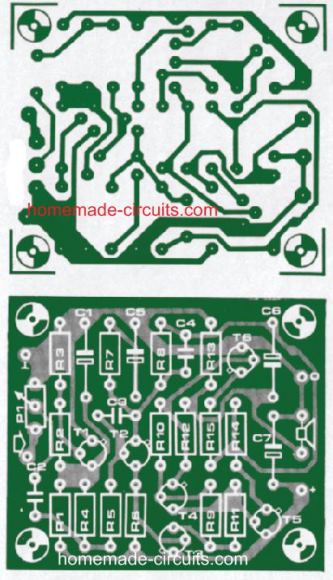
 In the modern times, one can find a lot of integrated circuit power amplifiers supplying outputs of 1 to 3 watts although the majority of them demand cautious layout of the circuit so that you can avoid instability (an unstable amplifier might vibrate and become destroyed consequently).
Furthermore, a discrete transistor amplifier is much more informative because voltages could be assessed to get a greater perception of its working.
Hence the present small amplifier is developed applying discrete transistors that apart from being far more steady than IC based designs, is perfectly suited to the requirements of the user.
Transistors Q2, Q4 and Q5 are cemented into a small aluminium that works as a heatsink.
In the modern times, one can find a lot of integrated circuit power amplifiers supplying outputs of 1 to 3 watts although the majority of them demand cautious layout of the circuit so that you can avoid instability (an unstable amplifier might vibrate and become destroyed consequently).
Furthermore, a discrete transistor amplifier is much more informative because voltages could be assessed to get a greater perception of its working.
Hence the present small amplifier is developed applying discrete transistors that apart from being far more steady than IC based designs, is perfectly suited to the requirements of the user.
Transistors Q2, Q4 and Q5 are cemented into a small aluminium that works as a heatsink.
 This small amplifier features a high input impedance of 1.1 megohm by ensuring that the Q1 transistor's collector current is held low, and by incorporating a high amount of ac and dc feedback.
The input sensitivity of this small amplifier circuit is fine-tuned by adjusting the resistor R3 value.
The circuit also features a low 2.5 mA output quiescent current of the output which is perfectly stabilized through resistors R5 and R8. Using a 17.5 volt power supply the amplifier will be able to provide a nice little 2.5 watts over a 8 ohms.
The audio output may have a distortion level of no more than 1% at 1 kHz.
This small amplifier features a high input impedance of 1.1 megohm by ensuring that the Q1 transistor's collector current is held low, and by incorporating a high amount of ac and dc feedback.
The input sensitivity of this small amplifier circuit is fine-tuned by adjusting the resistor R3 value.
The circuit also features a low 2.5 mA output quiescent current of the output which is perfectly stabilized through resistors R5 and R8. Using a 17.5 volt power supply the amplifier will be able to provide a nice little 2.5 watts over a 8 ohms.
The audio output may have a distortion level of no more than 1% at 1 kHz.
 Once connected and powered, the small 5 watt amplifier will be able to boost the output to a much amplified over any 8 ohm 5 watt loudspeakers.
The 47K is used for adjusting the volume output of the amplifier, and the 22K preset is used for setting up the quiscent current of the amplifier.
The 22k preset must be adjusted by connecting a small 100mA lamp in series with the supply line.
And the input point A must shorted to ground.
Next, adjust the 22k preset until there no illumination present on the lamp.
The quiescent current of this amplifier is not set.
The lamp could be removed now, and the amplifier used normally for the amplifying the input signal.
Once connected and powered, the small 5 watt amplifier will be able to boost the output to a much amplified over any 8 ohm 5 watt loudspeakers.
The 47K is used for adjusting the volume output of the amplifier, and the 22K preset is used for setting up the quiscent current of the amplifier.
The 22k preset must be adjusted by connecting a small 100mA lamp in series with the supply line.
And the input point A must shorted to ground.
Next, adjust the 22k preset until there no illumination present on the lamp.
The quiescent current of this amplifier is not set.
The lamp could be removed now, and the amplifier used normally for the amplifying the input signal.
 D1 is used to provide a tiny standing bias to the output transistors, which, when combined with the rather significant levelof negative feedback, decreases cross-over distortion to an undetectable level.
The emitter follower output stage provides the circuit with a low output impedance, allowing the load to be driven effectively with large output currents.
Q4 drives the loudspeaker during positive going output cycles, whereas Q3 drives the speakerduring negative going output cycles.
D1 is used to provide a tiny standing bias to the output transistors, which, when combined with the rather significant levelof negative feedback, decreases cross-over distortion to an undetectable level.
The emitter follower output stage provides the circuit with a low output impedance, allowing the load to be driven effectively with large output currents.
Q4 drives the loudspeaker during positive going output cycles, whereas Q3 drives the speakerduring negative going output cycles.
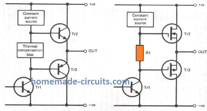 Comparing BJT vs MOSFET Amplifier Output Stage Configuration
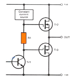 The thermally stabilized bias circuit could be substituted with a resistor because the temperature characteristics of power MOSFETs incorporates an in-built thermal control of the bias current at around 100 milliamps (which is approximately is the the best suited bias current).
An additional challenge experienced with BJTs is the rather low current gain of only 20 to 50. This can be quite insufficient for medium and high power ampliers.
Due to this it requires an extremely powerful driver stage.
The typical approach to solve this issue is to make use of a Darlington Pairs or an equivalent design to provide an adequately high current gain, so that it allows the employment of a low power driver stage.
Power MOSFETs, just like any FET device, tend to be voltage operated devices rather than current operated.
A power MOSFET's input impedance is typically very high which allows negligible input current draw with low working frequencies.
However, at high working frequencies the input impedance is a lot lower because of the relatively high input capacitance of approximately 500 pf.
Even with this high input capacitance a working current of hardly 10 milliamps becomes just enough through the driver stage, although the peak output current could be around one thousand times this quantity.
An additional problem with bipolar power devices (BJT) is their somewhat sluggish switching time.
This tends to create a variety of issues, such as slew triggered distortion.
This is when a powerful high frequency signal could demand a switching output voltage of let's say 2 volts per microsecond, while the BJT output stage may possibly allow a slew rate of only a volt per microsecond.
Naturally, the output will struggle to deliver a decent reproduction of the input signal, leading to an unavoidable distortion.
An inferior slew rate may also give an amplier an undesirable power bandwidth, with the highest achievable power output dropping significantly at higher audio frequencies.
The thermally stabilized bias circuit could be substituted with a resistor because the temperature characteristics of power MOSFETs incorporates an in-built thermal control of the bias current at around 100 milliamps (which is approximately is the the best suited bias current).
An additional challenge experienced with BJTs is the rather low current gain of only 20 to 50. This can be quite insufficient for medium and high power ampliers.
Due to this it requires an extremely powerful driver stage.
The typical approach to solve this issue is to make use of a Darlington Pairs or an equivalent design to provide an adequately high current gain, so that it allows the employment of a low power driver stage.
Power MOSFETs, just like any FET device, tend to be voltage operated devices rather than current operated.
A power MOSFET's input impedance is typically very high which allows negligible input current draw with low working frequencies.
However, at high working frequencies the input impedance is a lot lower because of the relatively high input capacitance of approximately 500 pf.
Even with this high input capacitance a working current of hardly 10 milliamps becomes just enough through the driver stage, although the peak output current could be around one thousand times this quantity.
An additional problem with bipolar power devices (BJT) is their somewhat sluggish switching time.
This tends to create a variety of issues, such as slew triggered distortion.
This is when a powerful high frequency signal could demand a switching output voltage of let's say 2 volts per microsecond, while the BJT output stage may possibly allow a slew rate of only a volt per microsecond.
Naturally, the output will struggle to deliver a decent reproduction of the input signal, leading to an unavoidable distortion.
An inferior slew rate may also give an amplier an undesirable power bandwidth, with the highest achievable power output dropping significantly at higher audio frequencies.
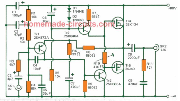 Tr1 is rigged as a common emitter input stage, directly connected to the Tr3 common emitter driver stage.
Both of these stages offer the total voltage gain of the amplier, and include a extremely large total gain.
Tr2 along with its attached parts create a simple constant current generator which has a marginal output current of 10 milliamps.
This works like the main collector load for Tr3.
R10 is employed to establish the correct quiescent bias current via the output transistors, and as discussed previously, the thermal stabilization for the bias current is not really accomplished in the bias circuit, but rather it is delivered by the output devices themselves.
R8 delivers practically 100% negative feedback from the amplifier output to Tr1 emitter, allowing the circuit just around an unity voltage gain.
Resistors R1, R2 and R4 work like a potential divider network for biasing the amplier input stage, and consequently the output also, to roughly around half the supply voltage.
This enables highest achievable output level before clipping and the start of critical distortion.
R1 and C2 are used like a filter circuit that cancels hum frequency and other forms of potential noises on the supply lines from entering the amplier input via the bias circuit.
R3 and C5 act like an RF filter which prevents RF signals busting right from input to output, causing audible disturbances.
C4 also aids to solving the same issue by rolling-off the amplifier's high frequency response effectively over the upper audio frequency limit.
To ensure that the amplifier gets a good voltage gain at audible frequencies it becomes essential to decouple the negative feedback to some extent.
C7 fulfils the role of the decoupling capacitor, while the R6 resistor limits the quantity of feedback which is cleaned up.
The circuit's voltage gain is approximately determined by dividing R8 by R6, or around 20 times (26dB) with the assigned part values.
The amplifier's maximum output voltage will be 16 volts RMS, which allows an input sensitivity of roughly around 777mV RMS for achieving a full output.
The input impedance could be more than 20k.
C3 and C8 are employed as the input and output coupling capacitors respectively.
C1 enables decoupling for the supply DC.
R11 and C9 exclusively serve to facilitate and control stability of the amplifier, by working like the popular Zobel network, which are often found around the output stages of most semiconductor power ampliers designs.
Tr1 is rigged as a common emitter input stage, directly connected to the Tr3 common emitter driver stage.
Both of these stages offer the total voltage gain of the amplier, and include a extremely large total gain.
Tr2 along with its attached parts create a simple constant current generator which has a marginal output current of 10 milliamps.
This works like the main collector load for Tr3.
R10 is employed to establish the correct quiescent bias current via the output transistors, and as discussed previously, the thermal stabilization for the bias current is not really accomplished in the bias circuit, but rather it is delivered by the output devices themselves.
R8 delivers practically 100% negative feedback from the amplifier output to Tr1 emitter, allowing the circuit just around an unity voltage gain.
Resistors R1, R2 and R4 work like a potential divider network for biasing the amplier input stage, and consequently the output also, to roughly around half the supply voltage.
This enables highest achievable output level before clipping and the start of critical distortion.
R1 and C2 are used like a filter circuit that cancels hum frequency and other forms of potential noises on the supply lines from entering the amplier input via the bias circuit.
R3 and C5 act like an RF filter which prevents RF signals busting right from input to output, causing audible disturbances.
C4 also aids to solving the same issue by rolling-off the amplifier's high frequency response effectively over the upper audio frequency limit.
To ensure that the amplifier gets a good voltage gain at audible frequencies it becomes essential to decouple the negative feedback to some extent.
C7 fulfils the role of the decoupling capacitor, while the R6 resistor limits the quantity of feedback which is cleaned up.
The circuit's voltage gain is approximately determined by dividing R8 by R6, or around 20 times (26dB) with the assigned part values.
The amplifier's maximum output voltage will be 16 volts RMS, which allows an input sensitivity of roughly around 777mV RMS for achieving a full output.
The input impedance could be more than 20k.
C3 and C8 are employed as the input and output coupling capacitors respectively.
C1 enables decoupling for the supply DC.
R11 and C9 exclusively serve to facilitate and control stability of the amplifier, by working like the popular Zobel network, which are often found around the output stages of most semiconductor power ampliers designs.
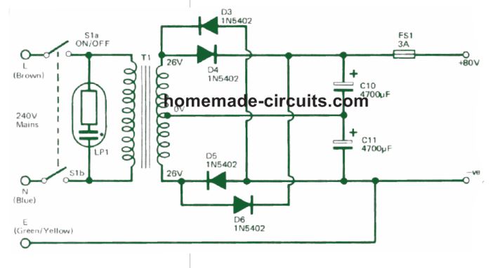 The image above demonstrates an appropriately configured power supply for the 35 watt MOSFET amplifier design.
The power supply may be adequately powerful to handle a mono or a stereo model of the unit.
The power supply is actually made up of an efficient a couple of push-pull rectier and smoothing circuits which have their outputs attached in series to provide a total output voltage corresponding to twice the potential applied by a individual rectier and capacitive filter circuit.
Diodes D4, D6 and C10 constitute one particular portion of the power supply while the second section is delivered by D3, D5 and C11. Each of these offer slightly below 40 volts without a load connected, and a total voltage of 80 V unloaded.
This value may drop to approximately 77 volts when the amplifier is loaded by a stereo input signal with a quiescent state operational, and to just around 60 volts when two amplifier channels are operated at full or maximum power.
The image above demonstrates an appropriately configured power supply for the 35 watt MOSFET amplifier design.
The power supply may be adequately powerful to handle a mono or a stereo model of the unit.
The power supply is actually made up of an efficient a couple of push-pull rectier and smoothing circuits which have their outputs attached in series to provide a total output voltage corresponding to twice the potential applied by a individual rectier and capacitive filter circuit.
Diodes D4, D6 and C10 constitute one particular portion of the power supply while the second section is delivered by D3, D5 and C11. Each of these offer slightly below 40 volts without a load connected, and a total voltage of 80 V unloaded.
This value may drop to approximately 77 volts when the amplifier is loaded by a stereo input signal with a quiescent state operational, and to just around 60 volts when two amplifier channels are operated at full or maximum power.
 This is meant for one channel of the amplier circuit, so naturally two such boards have to be assembled when a stereo amplier becomes necessary.
The output transistors are certainly not fitted on the PCB, rather over a large finned type.
It is not necessary to use mica insulation kit for the transistors while fixing them on the heatsink.
This is because the MOSFET sources are directly connected to their metal tabs, and these source pins have to be anyway remain connected to each other.
However, since they are not insulated from the heatsink it may be truly vital to ensure that the heatsinks do not come into an electrical contact with various other parts of the amplifier.
Also, for a stereo implementation the individual heatsinks employed for the a pair of ampliers should not be allowed to get into an electrical proximity with each other.
Always make sure to employ use shorter leads of a maximum of around 50 mm to hook up the output transistors with the PCB.
This is specifically crucial for the leads that connect with the gate terminals of the output MOSFETs.
Due to the fact that Power MOSFETs have high gain at high frequencies, longer leads may severely affect the stability response of the amplifier, or even trigger an RF oscillation which may in turn cause a permanent damage to the power MOSFETs.
Having said that, practically you may find hardly any difculty in preparing the design to ensure that these leads are effectively held shorter.
It may be important to note that C9 and R11 mounted outside the PCB, and are simply connected in series across the output socket.
This is meant for one channel of the amplier circuit, so naturally two such boards have to be assembled when a stereo amplier becomes necessary.
The output transistors are certainly not fitted on the PCB, rather over a large finned type.
It is not necessary to use mica insulation kit for the transistors while fixing them on the heatsink.
This is because the MOSFET sources are directly connected to their metal tabs, and these source pins have to be anyway remain connected to each other.
However, since they are not insulated from the heatsink it may be truly vital to ensure that the heatsinks do not come into an electrical contact with various other parts of the amplifier.
Also, for a stereo implementation the individual heatsinks employed for the a pair of ampliers should not be allowed to get into an electrical proximity with each other.
Always make sure to employ use shorter leads of a maximum of around 50 mm to hook up the output transistors with the PCB.
This is specifically crucial for the leads that connect with the gate terminals of the output MOSFETs.
Due to the fact that Power MOSFETs have high gain at high frequencies, longer leads may severely affect the stability response of the amplifier, or even trigger an RF oscillation which may in turn cause a permanent damage to the power MOSFETs.
Having said that, practically you may find hardly any difculty in preparing the design to ensure that these leads are effectively held shorter.
It may be important to note that C9 and R11 mounted outside the PCB, and are simply connected in series across the output socket.
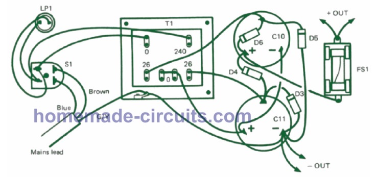 This actually looks pretty self-explanatory nevertheless it is ensured that the capacitors C10 and C11 both types consist of a dummy tag.
In case they aren't it can be crucial to employ a tag-strip to enable a few connection ports.
A solder-tag is Clipped to one particular mounting bolts of T1, which offers a chassis connection point for the mains AC earth lead.
This actually looks pretty self-explanatory nevertheless it is ensured that the capacitors C10 and C11 both types consist of a dummy tag.
In case they aren't it can be crucial to employ a tag-strip to enable a few connection ports.
A solder-tag is Clipped to one particular mounting bolts of T1, which offers a chassis connection point for the mains AC earth lead.
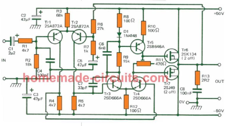 As shown above this circuit is designed with reference to a Hitachi layout.
Contrary to the last design, this circuit makes use of DC coupling for the loudspeaker and contains twin balanced power supply with a middle 0V and earth rail.
This enhancement gets rid of the dependency on big output coupling capacitors, as well as the under performance in low frequency performance this capacitor generates.
Furthermore, this layout also allows the circuit a decent supply ripple rejection capability.
Besides the DC coupling feature, the circuit design appears pretty distinct from that used in the earlier design.
Here, both the input and driver stages incorporate differential ampliers.
The input stage is configured using Tr1 and Tr2 while the driver stage is dependent on Tr3 and Tr4.
Transistor Tr5 is configured like a constant current collector load for Tr4. The signal path by means of the amplier commences using input coupling capacitor C1 , along with the RF lter R1/C4. R2 is used for biasing the amplifier's input on the central 0V supply track.
Tr1 is wired as an efficient a common emitter amplier which has its output directly connected to Tr4 which is applied as a common emitter driver stage.
From this stage onwards the audio signal is linked to Tr6 and Tr7 which are rigged as complementary source follower output stage.
The negative feedback is extracted from the amplifier output and connected with the Tr2 base, and despite of the fact that there's no signal inversion through the Tr1 base to the output of the amplifier, there does exist an inversion across the Tr2 base and the output.
It is because Tr2 working like an emitter follower perfectly drives the emitter of Tr1.
When an input signal is applied to the Tr1 emitter, the transistors successfully act like a common base stage.
Therefore, though the inversion does not take place by means of Tr1 and Tr2, inversion does happen through Tr4.
Also, phase change does not occur via the output stage, which means that the amplifier and the Tr2 base tend to be out-of-phase to execute the required required negative feedback.
The R6 and R7 values as suggested in the diagram provide a voltage gain of approximately 28 times.
As we learned from our previous discussions, a small disadvantage of power MOSFETs is they become less efcient than BJTs when they are wired through traditional Class B output stage.
Also, the relative efciency of power MOSFETs gets rather bad with high power circuits which demand gate/source voltage to be of several voltage for high source currents.
The maximum output voltage swing can be assumed to be equal to the supply voltage minus the maximum gate to source voltage of the individual transistor, and this certainly allows an output voltage swing which may be significantly lower than the supply voltage applied.
A straightforward means of getting higher efciency would be to basically incorporate a couple of similar MOSFETs attached in parallel across each of the output transistors.
The highest amount of current handled by each output MOSFETs will then be roughly reduced by half, and the maximum source to gate voltage of each MOSFET is lowered appropriately (along with a proportionate growth in the amplifier's output voltage swing).
However, a similar approach does not work when applied to bipolar devices, and this is essentially due to their positive temperature coefficient characteristics.
If one particular output BJT begins drawing excessive current than the other (because no two transistors will have exactly identical characteristic), one device begins getting more hot than the other.
This increased temperature causes the BJT's emitter/base threshold voltage getting reduced, and as a result it begins consuming a much larger portion of the output current.
The situation then causes the transistor to get hotter, and this process continues infinitely until one of the output transistor begins handling all the load, while the other remains inactive.
This kind of problem cannot be seen with power MOSFETs because of their negative temperature coefcient.
When one MOSFET begins getting hotter, due to its negative temperature coefficient the incresing heat begins restricting current flow through its drain/source.
This shifts the excess current towards the other MOSFET which now begins getting hotter, and quite similarly the heat causes the current through it to reduce proportionately.
The situation creates a balanced current share and dissipation across the devices making the amplifier working much efficient and reliable.
This phenomenon also allows MOSFETs to be connected in parallel simply by joining gate, source and drain leads together without much calculations or concerns.
As shown above this circuit is designed with reference to a Hitachi layout.
Contrary to the last design, this circuit makes use of DC coupling for the loudspeaker and contains twin balanced power supply with a middle 0V and earth rail.
This enhancement gets rid of the dependency on big output coupling capacitors, as well as the under performance in low frequency performance this capacitor generates.
Furthermore, this layout also allows the circuit a decent supply ripple rejection capability.
Besides the DC coupling feature, the circuit design appears pretty distinct from that used in the earlier design.
Here, both the input and driver stages incorporate differential ampliers.
The input stage is configured using Tr1 and Tr2 while the driver stage is dependent on Tr3 and Tr4.
Transistor Tr5 is configured like a constant current collector load for Tr4. The signal path by means of the amplier commences using input coupling capacitor C1 , along with the RF lter R1/C4. R2 is used for biasing the amplifier's input on the central 0V supply track.
Tr1 is wired as an efficient a common emitter amplier which has its output directly connected to Tr4 which is applied as a common emitter driver stage.
From this stage onwards the audio signal is linked to Tr6 and Tr7 which are rigged as complementary source follower output stage.
The negative feedback is extracted from the amplifier output and connected with the Tr2 base, and despite of the fact that there's no signal inversion through the Tr1 base to the output of the amplifier, there does exist an inversion across the Tr2 base and the output.
It is because Tr2 working like an emitter follower perfectly drives the emitter of Tr1.
When an input signal is applied to the Tr1 emitter, the transistors successfully act like a common base stage.
Therefore, though the inversion does not take place by means of Tr1 and Tr2, inversion does happen through Tr4.
Also, phase change does not occur via the output stage, which means that the amplifier and the Tr2 base tend to be out-of-phase to execute the required required negative feedback.
The R6 and R7 values as suggested in the diagram provide a voltage gain of approximately 28 times.
As we learned from our previous discussions, a small disadvantage of power MOSFETs is they become less efcient than BJTs when they are wired through traditional Class B output stage.
Also, the relative efciency of power MOSFETs gets rather bad with high power circuits which demand gate/source voltage to be of several voltage for high source currents.
The maximum output voltage swing can be assumed to be equal to the supply voltage minus the maximum gate to source voltage of the individual transistor, and this certainly allows an output voltage swing which may be significantly lower than the supply voltage applied.
A straightforward means of getting higher efciency would be to basically incorporate a couple of similar MOSFETs attached in parallel across each of the output transistors.
The highest amount of current handled by each output MOSFETs will then be roughly reduced by half, and the maximum source to gate voltage of each MOSFET is lowered appropriately (along with a proportionate growth in the amplifier's output voltage swing).
However, a similar approach does not work when applied to bipolar devices, and this is essentially due to their positive temperature coefficient characteristics.
If one particular output BJT begins drawing excessive current than the other (because no two transistors will have exactly identical characteristic), one device begins getting more hot than the other.
This increased temperature causes the BJT's emitter/base threshold voltage getting reduced, and as a result it begins consuming a much larger portion of the output current.
The situation then causes the transistor to get hotter, and this process continues infinitely until one of the output transistor begins handling all the load, while the other remains inactive.
This kind of problem cannot be seen with power MOSFETs because of their negative temperature coefcient.
When one MOSFET begins getting hotter, due to its negative temperature coefficient the incresing heat begins restricting current flow through its drain/source.
This shifts the excess current towards the other MOSFET which now begins getting hotter, and quite similarly the heat causes the current through it to reduce proportionately.
The situation creates a balanced current share and dissipation across the devices making the amplifier working much efficient and reliable.
This phenomenon also allows MOSFETs to be connected in parallel simply by joining gate, source and drain leads together without much calculations or concerns.
 An appropriately designed power supply circuit for the 120 watt MOSFET amplier is indicated above.
This looks much like the power supply circuit for our earlier design.
The only difference being the transformer centre tap supply at the junction of the two smoothing capacitors had been initially disregarded.
For the present example this is accustomed to provide the middle 0V earth supply, while the mains earth also hooks up at this junction instead of to the negative supply rail.
You can find fuses being installed across both the positive and negative rails.
The power output which is delivered by the amplier largely is dependent on the mains transformer specs.
For the majority of requirements a 35 ¡ª 0 ¡ª 35 volt 160VA toroidal mains transformer should be actually quite enough.
If stereo operation is preferred, the transformer will need to be replaced with a heavier 300 VA transformer.
Alternatively, isolated power supply units could be built using 160VA transformer each for each channel.
This allows a supply voltage of approximately 50 V at quiescent conditions, although at full load this level may drop to a much lower level.
This enables an output of up to around 70 watts RMS to be acquired through 8 ohm rated loudspeakers.
A crucial point to be noted is that the 1N5402 diodes used in the bridge rectifier have a maximum tolerable current rating of 3 amps.
This may be ample for a single channel amplier, but this may not be sufficient for a stereo version.
For a stereo version the diodes must be replaced with 6 amp diodes or a 6A4 diodes.
An appropriately designed power supply circuit for the 120 watt MOSFET amplier is indicated above.
This looks much like the power supply circuit for our earlier design.
The only difference being the transformer centre tap supply at the junction of the two smoothing capacitors had been initially disregarded.
For the present example this is accustomed to provide the middle 0V earth supply, while the mains earth also hooks up at this junction instead of to the negative supply rail.
You can find fuses being installed across both the positive and negative rails.
The power output which is delivered by the amplier largely is dependent on the mains transformer specs.
For the majority of requirements a 35 ¡ª 0 ¡ª 35 volt 160VA toroidal mains transformer should be actually quite enough.
If stereo operation is preferred, the transformer will need to be replaced with a heavier 300 VA transformer.
Alternatively, isolated power supply units could be built using 160VA transformer each for each channel.
This allows a supply voltage of approximately 50 V at quiescent conditions, although at full load this level may drop to a much lower level.
This enables an output of up to around 70 watts RMS to be acquired through 8 ohm rated loudspeakers.
A crucial point to be noted is that the 1N5402 diodes used in the bridge rectifier have a maximum tolerable current rating of 3 amps.
This may be ample for a single channel amplier, but this may not be sufficient for a stereo version.
For a stereo version the diodes must be replaced with 6 amp diodes or a 6A4 diodes.

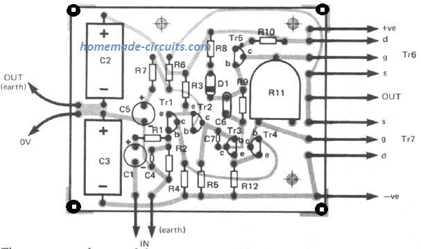
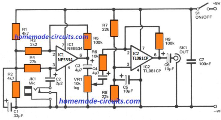 The microphone preamplier shown above features a voltage gain of over 52dB (400 times) which could suit a high impedance dynamic or electret microphone to just about any section of an audio gear.
If employed in association with standard microphones as mentioned here, an output of approximately 1 volt RMS could be easily obtained, although a gain control makes it possible for a lower output to be set to ensure that overloading of the circuit by the load could be eliminated.
The signal to noise ratio of the circuit is outstanding and is normally above 70 dB with respect to an output of 1 V RMS (with full gain and unloaded).
The microphone preamplier shown above features a voltage gain of over 52dB (400 times) which could suit a high impedance dynamic or electret microphone to just about any section of an audio gear.
If employed in association with standard microphones as mentioned here, an output of approximately 1 volt RMS could be easily obtained, although a gain control makes it possible for a lower output to be set to ensure that overloading of the circuit by the load could be eliminated.
The signal to noise ratio of the circuit is outstanding and is normally above 70 dB with respect to an output of 1 V RMS (with full gain and unloaded).

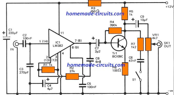
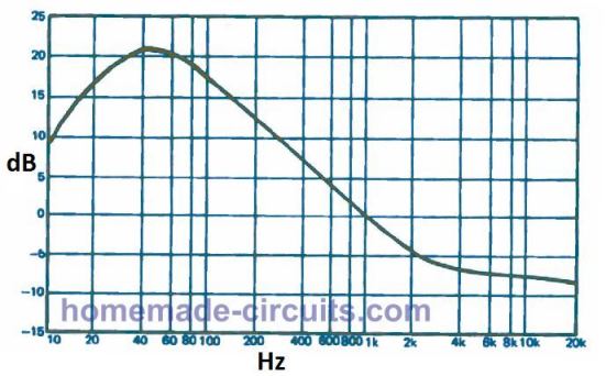 The process is implemented by applying treble boost however the quantity of boost adapted relies on the dynamic level of thesignal.
It is highest throughout low-signal intervals and decreases to zero at the maximum with dynamic level signals.
When a music signal is applied at the input, the circuit enables a treble cut which again is optimized dynamically, this actually occurs in order to compensate a high treble boost response.
The universal pre-amplifier circuit has a top cut filter using R7 and c8, which allows an attenuation of around 5 dB with 10 kHz frequencies.
Due to this the high frequencies can be boosted by a magnitude of 5 dB for high signal levels.
For medium signal inputs, the frequency response offered by the design is just flat.
The process is implemented by applying treble boost however the quantity of boost adapted relies on the dynamic level of thesignal.
It is highest throughout low-signal intervals and decreases to zero at the maximum with dynamic level signals.
When a music signal is applied at the input, the circuit enables a treble cut which again is optimized dynamically, this actually occurs in order to compensate a high treble boost response.
The universal pre-amplifier circuit has a top cut filter using R7 and c8, which allows an attenuation of around 5 dB with 10 kHz frequencies.
Due to this the high frequencies can be boosted by a magnitude of 5 dB for high signal levels.
For medium signal inputs, the frequency response offered by the design is just flat.
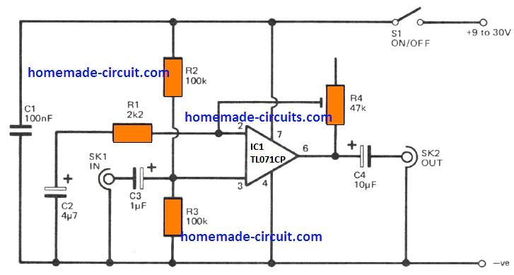 Amplifiers expressly built that can be used with guitars usually have a relatively high sensitivity and these could be used reliably for just about any pick-up, however when using a guitar with some other form of amplifier (such as a hi-fl amplifier) the overall volume achieved is always considered to be insufficient.
A easy remedy to this issue is to use a preamplifier as shown above, before feeding it to the power amplifier to raise the signal frequency amplitude.
The basic configuration mentioned here has a voltage gain that could really vary from unit to more than 26dB (20 times), therefore it should suit virtually every guitar pick-up to practically every power amplifier.
The preamplifier's input impedance should be about 50k, and the output impedance is low.
Therefore the circuit could be employedas a basic buffer amplifier with unity voltage gain to suit the fairly high output impedance of a guitar pick-up to a power amplifier havinga low input impedance if required.
A solitary low-noise BIFET operational amplifier (IC1) has been used as a basis for the unit, which therefore has marginal distortion levels as well as a signal-to-noise ratio of around -70dB or highereven when the unit orkswwith a very low output instrument like a guitar.
Amplifiers expressly built that can be used with guitars usually have a relatively high sensitivity and these could be used reliably for just about any pick-up, however when using a guitar with some other form of amplifier (such as a hi-fl amplifier) the overall volume achieved is always considered to be insufficient.
A easy remedy to this issue is to use a preamplifier as shown above, before feeding it to the power amplifier to raise the signal frequency amplitude.
The basic configuration mentioned here has a voltage gain that could really vary from unit to more than 26dB (20 times), therefore it should suit virtually every guitar pick-up to practically every power amplifier.
The preamplifier's input impedance should be about 50k, and the output impedance is low.
Therefore the circuit could be employedas a basic buffer amplifier with unity voltage gain to suit the fairly high output impedance of a guitar pick-up to a power amplifier havinga low input impedance if required.
A solitary low-noise BIFET operational amplifier (IC1) has been used as a basis for the unit, which therefore has marginal distortion levels as well as a signal-to-noise ratio of around -70dB or highereven when the unit orkswwith a very low output instrument like a guitar.
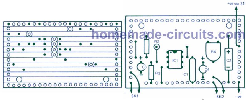
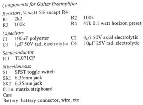
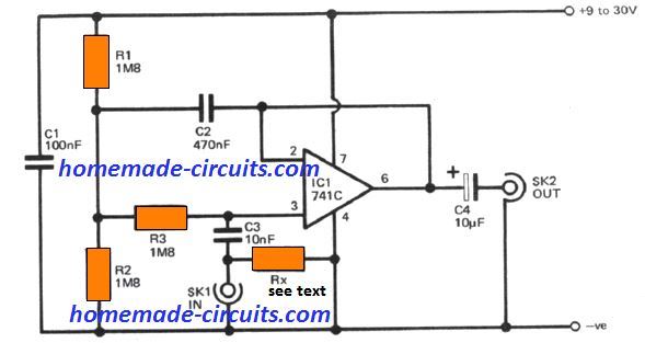
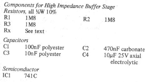

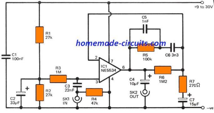 In earlier days, the output of a moving coil cartridge of a magnet or high voltage was typically 2.5 to 10 millivolt range, so that the pickup could bebalanced with the power amplifier (this would possibly require an output signal of a coupleof hundred millivolts RMS).
Although the output of magnetic and moving coil cartridges would rise at 6dB per octave it could do without the need of any equalization to counteract this since suitable equalization had to be involved during the recording process.
Nevertheless, equalization would bestill necessary because during the recording process bass cut and treble boost would be used, in addition to adjusting, the frequency response often counteracted with a 6dB octave increase in pick-up output.
The bass cut had to be includedto stop unnecessarily low-frequency groove modulations and the triple boost (with triple cut in playback) would provide a simple but efficient noise reduction facility.
In earlier days, the output of a moving coil cartridge of a magnet or high voltage was typically 2.5 to 10 millivolt range, so that the pickup could bebalanced with the power amplifier (this would possibly require an output signal of a coupleof hundred millivolts RMS).
Although the output of magnetic and moving coil cartridges would rise at 6dB per octave it could do without the need of any equalization to counteract this since suitable equalization had to be involved during the recording process.
Nevertheless, equalization would bestill necessary because during the recording process bass cut and treble boost would be used, in addition to adjusting, the frequency response often counteracted with a 6dB octave increase in pick-up output.
The bass cut had to be includedto stop unnecessarily low-frequency groove modulations and the triple boost (with triple cut in playback) would provide a simple but efficient noise reduction facility.
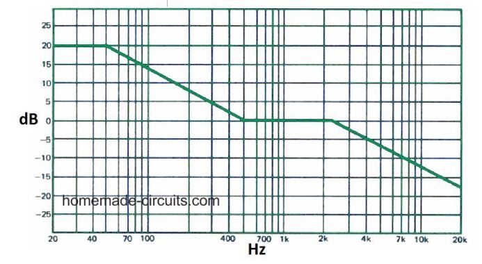 Figure above is actually a typical old RIAA preamplifier circuit's frequency response graph which shows the necessary parameters required for successfully implementing a highly sensitive preamplifier such as this.
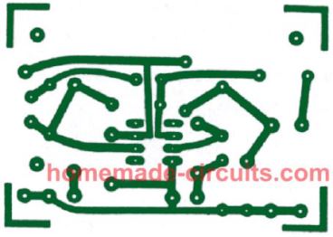
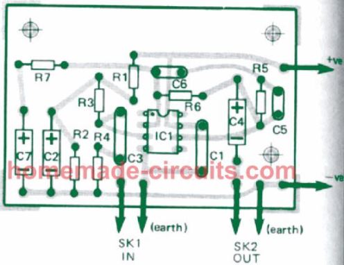
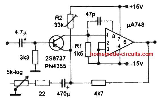 Overriding the input differential pair of the IC 748, as indicated, gets rid of potential instability.
The transistor is determined for any low noise attribute while driven from a 200 Ohm source, its collector current being variable for complementing exactly the same.
The high stability MIC circuit using just one op amp is exceptional due to its low noise, high stability and reduced distortion, despite the pretty simple dynamics of the circuit and having only a general-purpose op-amp.
Resistor R2 is positioned for adjusting the symmetry of the circuit.
Overriding the input differential pair of the IC 748, as indicated, gets rid of potential instability.
The transistor is determined for any low noise attribute while driven from a 200 Ohm source, its collector current being variable for complementing exactly the same.
The high stability MIC circuit using just one op amp is exceptional due to its low noise, high stability and reduced distortion, despite the pretty simple dynamics of the circuit and having only a general-purpose op-amp.
Resistor R2 is positioned for adjusting the symmetry of the circuit.
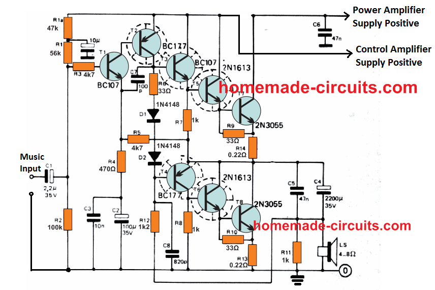
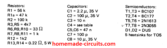
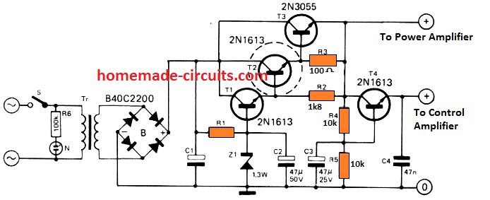 IN THIS CIRCUIT ONLY T2 WILL NEED A HEATSINK
Parts List for the power supply is as per the following data:
IN THIS CIRCUIT ONLY T2 WILL NEED A HEATSINK
Parts List for the power supply is as per the following data:
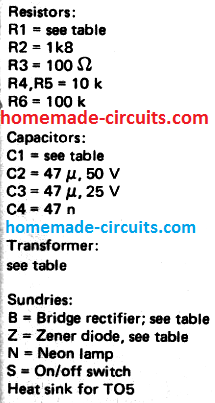 Transformer, bridge rectifier, filter capacitor, zener diode and the resistor R1 will have different values, depending upon the supply voltage, power output and loudspeaker selection for the amplifier.
The following table gives us the exact values of these elements as per the selection preference of the user.
Transformer, bridge rectifier, filter capacitor, zener diode and the resistor R1 will have different values, depending upon the supply voltage, power output and loudspeaker selection for the amplifier.
The following table gives us the exact values of these elements as per the selection preference of the user.
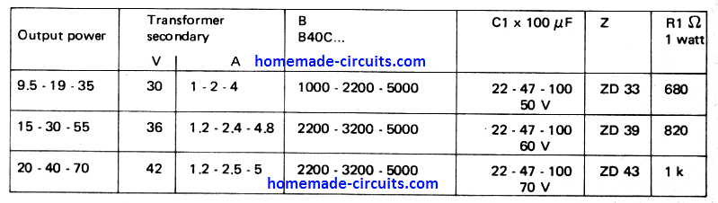
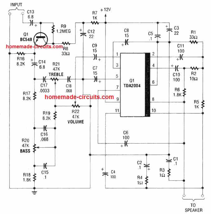 The design is low-cost and can perform for almost all power amplifier applications.
This can work really well for applications like an intercom, a PA system, or, more than likely, an obvious traditional type of audio amplifier.
You are going to naturally require a couple of these modules to build a stereo 30 + 30 watt audio, still the price must not be a matter of concern.
The amplifier is made using the TDA2004 audio-amplifier IC, as indicated in the circuit diagram, supplies 30 watts peak, 15 watts RMS, therefore it can easily work with 4 to 8 ohm speakers.
Then of course you'll have to have a 12 volt DC, 2 amp power supply also to power the amplifier.
The one particular demonstrated in the following diagram will perform perfectly.
The design is low-cost and can perform for almost all power amplifier applications.
This can work really well for applications like an intercom, a PA system, or, more than likely, an obvious traditional type of audio amplifier.
You are going to naturally require a couple of these modules to build a stereo 30 + 30 watt audio, still the price must not be a matter of concern.
The amplifier is made using the TDA2004 audio-amplifier IC, as indicated in the circuit diagram, supplies 30 watts peak, 15 watts RMS, therefore it can easily work with 4 to 8 ohm speakers.
Then of course you'll have to have a 12 volt DC, 2 amp power supply also to power the amplifier.
The one particular demonstrated in the following diagram will perform perfectly.
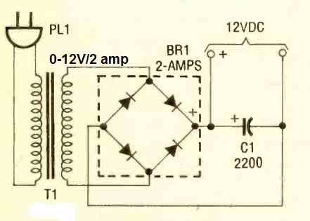
 Transistors T1 and T2 are designed to function like a high input impedance voltage amplifier and with a low output impedance.
When the central slider arm of the preset P1 is adjusted to its full 1 k limit, the input sensitivity along with the small 5 watt amplifier gets to around 150 mV for the 12 -volt version, and when a 4 ohm speaker is used as the load.
This may become 200 mV if the supply voltage is increased to 17 V and the speaker is of 8 ohm value.
If you need a greater input sensitivity, you can use the preset P1 value lower than 1 K.
If you are interested to include a selective range for the input sensitivity, in that case you can put a selector switch with different resistors at the input for selecting the desired input sensitivity range.
The formula for calculating the resistor values is shown below:
Rx = 500 x Vin / 300 - Vin
where Vin depicts the input RMS value of the voltage in mV.
The formula can be effectively used for all input voltages ranging from 5 mV to 250 mV.
The transistors T3 is configured as a Baxandall tone control circuit.
The 1 nF capacitor between T3 collector and ground line is included to improve stabilization and restrict oscillations.
Transistors T1 and T2 are designed to function like a high input impedance voltage amplifier and with a low output impedance.
When the central slider arm of the preset P1 is adjusted to its full 1 k limit, the input sensitivity along with the small 5 watt amplifier gets to around 150 mV for the 12 -volt version, and when a 4 ohm speaker is used as the load.
This may become 200 mV if the supply voltage is increased to 17 V and the speaker is of 8 ohm value.
If you need a greater input sensitivity, you can use the preset P1 value lower than 1 K.
If you are interested to include a selective range for the input sensitivity, in that case you can put a selector switch with different resistors at the input for selecting the desired input sensitivity range.
The formula for calculating the resistor values is shown below:
Rx = 500 x Vin / 300 - Vin
where Vin depicts the input RMS value of the voltage in mV.
The formula can be effectively used for all input voltages ranging from 5 mV to 250 mV.
The transistors T3 is configured as a Baxandall tone control circuit.
The 1 nF capacitor between T3 collector and ground line is included to improve stabilization and restrict oscillations.
 Component track layout for the above stereo compact PCB
 Transistors TI and 12 are wired as a Darlington pair so that it works like a composite high gain, high power emitter follower transistor.
The base reference voltage for this emitter follower is fixed through Z1 which may be selected as a 13 V or 18 volt zener for getting a 12 V or 17 volt supply respectively.
Due to lower input output differential T2 is supposed to dissipate very little amount of power as heat and therefore a heatsink may not be essential.
Transistors TI and 12 are wired as a Darlington pair so that it works like a composite high gain, high power emitter follower transistor.
The base reference voltage for this emitter follower is fixed through Z1 which may be selected as a 13 V or 18 volt zener for getting a 12 V or 17 volt supply respectively.
Due to lower input output differential T2 is supposed to dissipate very little amount of power as heat and therefore a heatsink may not be essential.
 Parts List
 Another flaw with LM386 is its input impedance which seems to be very high, allowing the chip to be much vulnerable to oscillations if the inputs are not sufficiently isolated from the output.
Its voltage gain of 20 (or 200 by inserting an additional capacitor) looks quite high for line input level (1 V RMS) and this results in further oscillation issues.
On the other hand, the LM4862 IC is more advanced and slightly more powerful compared to LM386 and it works without any electrolytic capacitor.
Another flaw with LM386 is its input impedance which seems to be very high, allowing the chip to be much vulnerable to oscillations if the inputs are not sufficiently isolated from the output.
Its voltage gain of 20 (or 200 by inserting an additional capacitor) looks quite high for line input level (1 V RMS) and this results in further oscillation issues.
On the other hand, the LM4862 IC is more advanced and slightly more powerful compared to LM386 and it works without any electrolytic capacitor.
 It looks very simple without the use of any electrolytic capacitors; which allows it to be cheap and yet have a high-fidelity audio output.
Basically, C2, works like the bias bypass capacitor, which can be a tantalum electrolytic; blocks the audio signal through it.
If possible a 100 ¦ÌF electrolytic could be added parallel with the C3 to increase stability when the IC is operated with batteries or a poorly regulated power supply.
The voltage gain is determined by 2(R2 /R1) that must not be exceed the value of 20.
You can expect the sound quality to be the best when R2 = R1 and the gain is 2. This is exactly what must be followed to drive a speaker when the input is 1 volt from a line input or a headphone jack 3.5 mm.
In case the gain is made higher than 5, it may be necessary to add a bypass capacitor C4 across R2 to prevent oscillation.
This can be a 5 pF capacitor, although up to 22 pF capacitor can also be used.
But higher values than this may cause problems.
Typically, smaller value resistors can be used like R1 = 4.7K and R2 = 4.7K to 47K, when the input is fed from a low impedance supply.
The following image shows us the component values for a few typical typical amplifier set ups.
It looks very simple without the use of any electrolytic capacitors; which allows it to be cheap and yet have a high-fidelity audio output.
Basically, C2, works like the bias bypass capacitor, which can be a tantalum electrolytic; blocks the audio signal through it.
If possible a 100 ¦ÌF electrolytic could be added parallel with the C3 to increase stability when the IC is operated with batteries or a poorly regulated power supply.
The voltage gain is determined by 2(R2 /R1) that must not be exceed the value of 20.
You can expect the sound quality to be the best when R2 = R1 and the gain is 2. This is exactly what must be followed to drive a speaker when the input is 1 volt from a line input or a headphone jack 3.5 mm.
In case the gain is made higher than 5, it may be necessary to add a bypass capacitor C4 across R2 to prevent oscillation.
This can be a 5 pF capacitor, although up to 22 pF capacitor can also be used.
But higher values than this may cause problems.
Typically, smaller value resistors can be used like R1 = 4.7K and R2 = 4.7K to 47K, when the input is fed from a low impedance supply.
The following image shows us the component values for a few typical typical amplifier set ups.
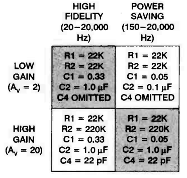 Note that, the design of the amplifier becomes more efficient in terms of cost and power saving when the bass response is kept at its minimum, although that would also mean the absence of the heavier low frequency notes.
The LM4862 is specified to work with at least a 8 ohm speaker, lower ohms might also work such as 16 ohm, 32 ohm, or 64 ohm speaker, but that may cause the power output to be significantly less.
If you wish to operate the speaker as a single ended output by grounding its one end, you might need to add a series capacitor with the other end of the speaker which is connected with the IC output as shown below:
Note that, the design of the amplifier becomes more efficient in terms of cost and power saving when the bass response is kept at its minimum, although that would also mean the absence of the heavier low frequency notes.
The LM4862 is specified to work with at least a 8 ohm speaker, lower ohms might also work such as 16 ohm, 32 ohm, or 64 ohm speaker, but that may cause the power output to be significantly less.
If you wish to operate the speaker as a single ended output by grounding its one end, you might need to add a series capacitor with the other end of the speaker which is connected with the IC output as shown below:
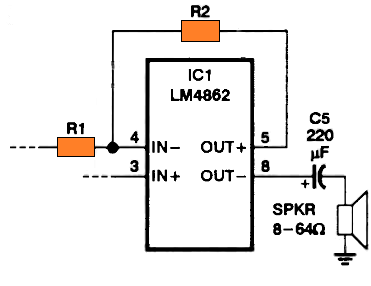 But single ended operation may drastically reduce the power output from the speaker compared to the differential mode.
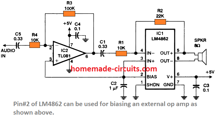 It may be necessary to bypass the bias pin to ground using any capacitor from 0.1 and 10 ¦ÌF for improving ripple rejection response and also to suppress the "thump" sound each time the amplifier is switched on.
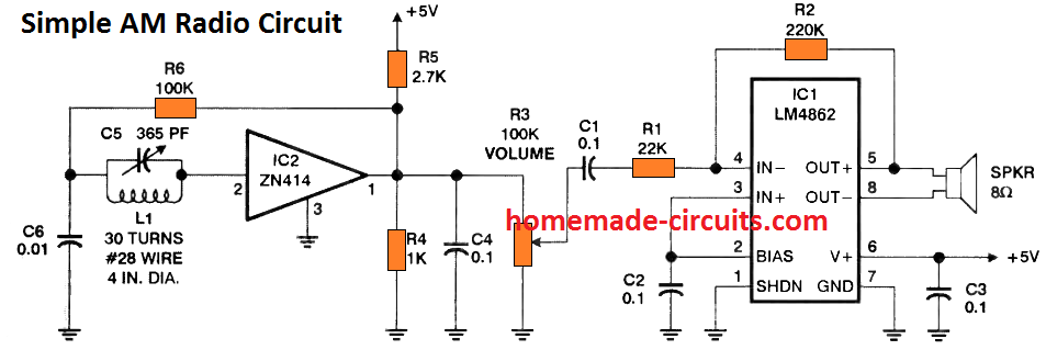 This simple radio will receive all the local AM stations loud and clear over the attached loudspeaker
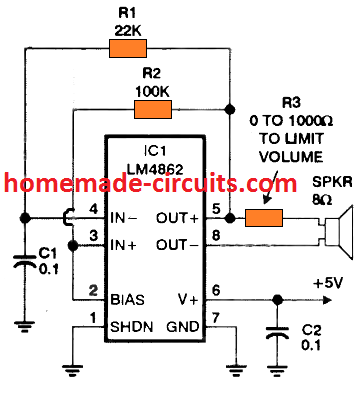
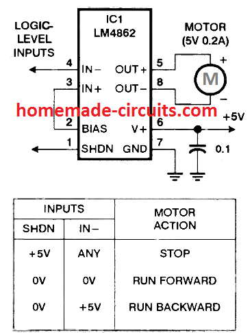 Reference: http://www.ti.com/lit/ds/symlink/lm4862.pdf
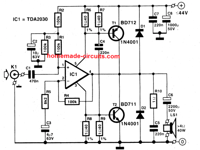

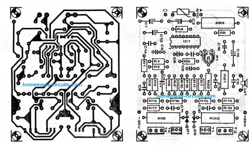 Parts List
 For more info on this please visit the datasheet of the IC
 DOWNLOAD PCB LAYOUT
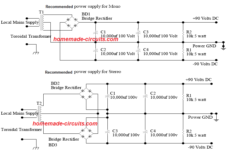
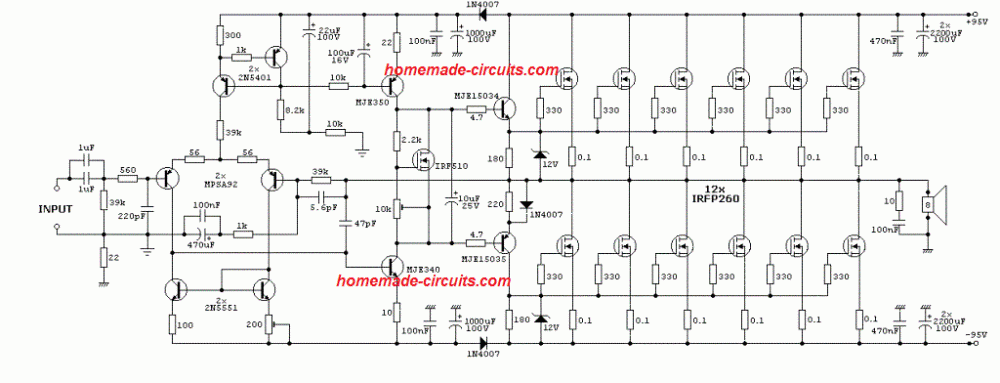
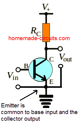 Basically, here the transistor base terminal is used as the input, the collector is configured as the output, and the emitter is wired commonto both (for example, if the transistor is NPN the emitter may be joined tothe ground line reference), hence it gets its name as the common emitter.
For an FET, the analogouscircuit is termed as thecommon-sourceamplifier.
Basically, here the transistor base terminal is used as the input, the collector is configured as the output, and the emitter is wired commonto both (for example, if the transistor is NPN the emitter may be joined tothe ground line reference), hence it gets its name as the common emitter.
For an FET, the analogouscircuit is termed as thecommon-sourceamplifier.
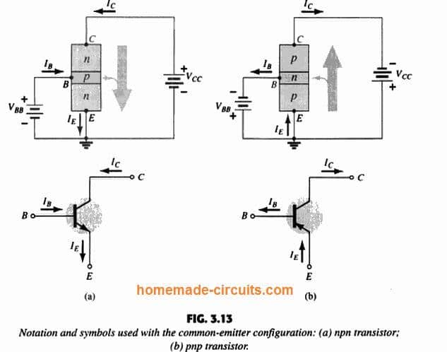 The current flow directions for the emitter, collector and base are indicated as per the standard conventional rule.
Although, the configuration has changed, the relationship for the current flow which was established in our previous common base configuration still applies here without any modifications.
This may be represented as:IE = IC + IB and IC =IE.
For our present common-emitter configuration, the indicated output characteristics are a graphical representation of the output current (IC) versus output voltage (VCE) for a selected set of values of input current (IB).
The input characteristics can be seen as a plotting of input current (IB) against the input voltage (VBE) for a given set of output voltage values (VCE)
The current flow directions for the emitter, collector and base are indicated as per the standard conventional rule.
Although, the configuration has changed, the relationship for the current flow which was established in our previous common base configuration still applies here without any modifications.
This may be represented as:IE = IC + IB and IC =IE.
For our present common-emitter configuration, the indicated output characteristics are a graphical representation of the output current (IC) versus output voltage (VCE) for a selected set of values of input current (IB).
The input characteristics can be seen as a plotting of input current (IB) against the input voltage (VBE) for a given set of output voltage values (VCE)
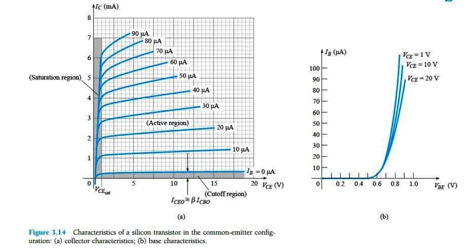 Observe that the characteristics of Fig.
3.14 indicates the value of IB in microamperes, instead of milliamperes for IC.
Also we find that the curves of IB are not perfectly horizontal like the ones achieved for IE in the common-base configuration, which implies that the collector-to-emitter voltage has the ability to affect the value of the base current.
The active region for the common-emitter configuration can be understood as that section of the upper-right quadrant which owns the largest amount of linearity, meaning, that specific area where the curves for IB tend to be practically straight and evenly spread out.
In Fig.
3.14a this region could be witnessed on the right side of the vertical dashed line at VCEsat and over the curve of IB equal to zero.
The region on the left of VCEsat is known as the saturation region.
Within the active region of a common-emitter amplifier the collector-base junction will be reverse-biased, while the base-emitter junction will be forward-biased.
If you remember these were exactly the same factors which persisted in the active region of the common-base setup.
The active region of the common-emitter configuration could be implemented for voltage, current, or power amplification.
The cutoff region for the common-emitter configuration doesn't appear to be nicely characterized compared to that of the common-base configuration.
Notice that in the collector characteristics of Fig.
3.14 the IC is not really corresponding to zero while IB is zero.
For the common-base configuration, whenever the input current IE happens to be near zero, the collector current becomes equal only to the reverse saturation current ICO, in order that the curve IE= 0 and the voltage axis were one, for all practical applications.
The cause for this variation in collector characteristics could be evaluated with the appropriate modifications of Eqs.
(3.3) and (3.6).
as given below:
Observe that the characteristics of Fig.
3.14 indicates the value of IB in microamperes, instead of milliamperes for IC.
Also we find that the curves of IB are not perfectly horizontal like the ones achieved for IE in the common-base configuration, which implies that the collector-to-emitter voltage has the ability to affect the value of the base current.
The active region for the common-emitter configuration can be understood as that section of the upper-right quadrant which owns the largest amount of linearity, meaning, that specific area where the curves for IB tend to be practically straight and evenly spread out.
In Fig.
3.14a this region could be witnessed on the right side of the vertical dashed line at VCEsat and over the curve of IB equal to zero.
The region on the left of VCEsat is known as the saturation region.
Within the active region of a common-emitter amplifier the collector-base junction will be reverse-biased, while the base-emitter junction will be forward-biased.
If you remember these were exactly the same factors which persisted in the active region of the common-base setup.
The active region of the common-emitter configuration could be implemented for voltage, current, or power amplification.
The cutoff region for the common-emitter configuration doesn't appear to be nicely characterized compared to that of the common-base configuration.
Notice that in the collector characteristics of Fig.
3.14 the IC is not really corresponding to zero while IB is zero.
For the common-base configuration, whenever the input current IE happens to be near zero, the collector current becomes equal only to the reverse saturation current ICO, in order that the curve IE= 0 and the voltage axis were one, for all practical applications.
The cause for this variation in collector characteristics could be evaluated with the appropriate modifications of Eqs.
(3.3) and (3.6).
as given below:
 Assessing the above discussed scenario, where IB = 0 A, and by replacing a typical value like 0.996 for ¦Á, we are able to achieve a resultant collector current as expressed below:
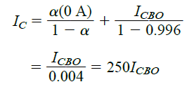 If we consider ICBO as 1 ¦ÌA, the resulting collector current with IB = 0 A would be 250(1 ¦ÌA) = 0.25 mA, as reproduced in the characteristics of Fig.
3.14.
In all our future discussions, the collector current established by the condition IB = 0 ¦ÌA will have the notation as determined by the following Eq.
(3.9).
If we consider ICBO as 1 ¦ÌA, the resulting collector current with IB = 0 A would be 250(1 ¦ÌA) = 0.25 mA, as reproduced in the characteristics of Fig.
3.14.
In all our future discussions, the collector current established by the condition IB = 0 ¦ÌA will have the notation as determined by the following Eq.
(3.9).
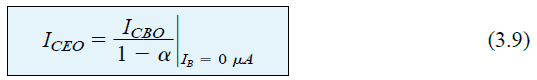 The conditions based on the above newly establish current could be visualized in the following Fig 3.15 usingits reference directions as outlined above.
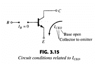 For enabling amplification with minimum distortions in the common emitter mode, the cut off is established by the collector current IC = ICEO.
It means the area just underIB = 0 ¦ÌA should be avoided for ensuring a clean and an undistorted output from the amplifier.
For enabling amplification with minimum distortions in the common emitter mode, the cut off is established by the collector current IC = ICEO.
It means the area just underIB = 0 ¦ÌA should be avoided for ensuring a clean and an undistorted output from the amplifier.
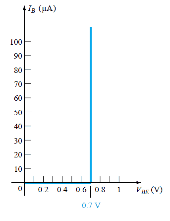 Figure 3.16 Piecewise-linear equivalent for the diode characteristics of Fig.
3.14b.
The result complies with or our previous deduction according to which the base emitter voltage for a BJT within the active region or the ON state will be 0.7V, and this will be fixed regardless of the base current.
Figure 3.16 Piecewise-linear equivalent for the diode characteristics of Fig.
3.14b.
The result complies with or our previous deduction according to which the base emitter voltage for a BJT within the active region or the ON state will be 0.7V, and this will be fixed regardless of the base current.
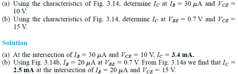
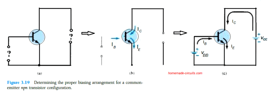 Biasing a common-emitter amplifier appropriately could be established in the same way as it was implemented for the common-base network.
Suppose you had a npn transistor just as indicated in Fig.
3.19a, and wanted to enforce a correct biasing through it, in order to establish the BJT in the active region.
For this you would require to first indicate the IE direction as proven by the arrow marks in the symbol of the transistor (see Fig.
3.19b).
After this, you'd require establishing the other current directions strictly as perKirchhoff¡¯s current law relationship: IC + IB = IE.
Subsequently, you have to introduce the supply lines with correct polarities complementing the directions of IB and IC as indicated in Fig.
3.19c, and finally conclude the procedure.
In the similar manner a pnp BJT could be also biased in its common emitter mode, for this you simply have to reverse all the polarities of the Fig.
3.19
Biasing a common-emitter amplifier appropriately could be established in the same way as it was implemented for the common-base network.
Suppose you had a npn transistor just as indicated in Fig.
3.19a, and wanted to enforce a correct biasing through it, in order to establish the BJT in the active region.
For this you would require to first indicate the IE direction as proven by the arrow marks in the symbol of the transistor (see Fig.
3.19b).
After this, you'd require establishing the other current directions strictly as perKirchhoff¡¯s current law relationship: IC + IB = IE.
Subsequently, you have to introduce the supply lines with correct polarities complementing the directions of IB and IC as indicated in Fig.
3.19c, and finally conclude the procedure.
In the similar manner a pnp BJT could be also biased in its common emitter mode, for this you simply have to reverse all the polarities of the Fig.
3.19
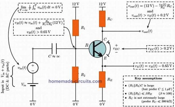 The AC-coupled circuit functions like a level-shifter amplifier.
In this situation, , the base¨Cemitter voltage drop is supposed to be around 0.7 volts.
The input capacitor C gets rid of any DC element of the input, while the resistors R1 and R2 are used for biasing the transistor to enable it to be in active condition for the whole range of the input.
The output is an upside down replication of the AC component of the input which has been boosted by the ratio RC/RE and moved through a measure decided by all 4 resistors.
Due to the fact RC is normally quite massive, the output impedance on this circuit could be really substantial.
To minimize this concern, RC is maintained as small as it can be plus the amplifier is accompanied by a voltage buffer such as an emitter follower.
The AC-coupled circuit functions like a level-shifter amplifier.
In this situation, , the base¨Cemitter voltage drop is supposed to be around 0.7 volts.
The input capacitor C gets rid of any DC element of the input, while the resistors R1 and R2 are used for biasing the transistor to enable it to be in active condition for the whole range of the input.
The output is an upside down replication of the AC component of the input which has been boosted by the ratio RC/RE and moved through a measure decided by all 4 resistors.
Due to the fact RC is normally quite massive, the output impedance on this circuit could be really substantial.
To minimize this concern, RC is maintained as small as it can be plus the amplifier is accompanied by a voltage buffer such as an emitter follower.
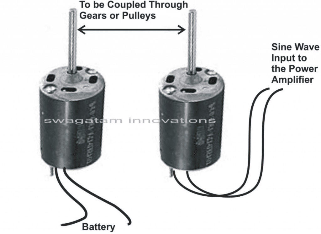


 Parts List
All resistors 1/4 watt or 1/8 watt, 1% MFR or SMD
20 K = 2 nos
100 K = 1 no (Rpu)
Capacitors
0.39uF ceramic = 1 no
1uF / 16V Tantalum = 2 nos
Semiconductor
IC LM4871 = 1 no
As can be seen in the above schematic, the LM4871 includes a couple of operational amplifiers internally, providing the user the option of configuring the amplifier through a few specified ways.
The gain of the first amplifier can be managed externally, while the second amplifier has been wired up internally with an inverting unity gain.
The closed loop gain for the first amplifier can be determined by appropriately selecting the values of the ratio Rf/Ri, whereas the same has been fixed for the second amplifier internally through a couple of 40K resistors.
We can see that the output of the amplifier#1 is configured to be the input of amplifier#2, allowing both the amplifiers to generate signals with identical values, although these may be 180 degrees out of phase.
This results in the IC¡¯s differential gain to be AVD= 2 *(Rf /Ri ) .
Typically, for any amplifier a ¡°bridged mode¡± set up can be implemented by driving the connected load deferentially via a couple of outputs Vo1 and Vo2.
An amplifier configured in the bridged mode will have a different operating principle in contrast to the traditional single ended amplifiers which have one end of the load wired with the ground line.
A bridged mode circuit works with better efficiency compared to a single ended amplifier since the load or the loudspeaker is switched in a push-pull manner, enabling a double voltage swing for each alternate frequency pulse.
This actually allows the loudspeaker to produce 4 times more power than a single ended version under identical circumstances or specifications.
The ability to achieve such increased power allows the amplifier to work without a current limiter stage and hence without undesirable clipping.
An added benefit of differential bridged output is the absence of net DC across the connected loudspeaker.
This happens since VO1 and VO1 are biased at identical voltage levels, that is VDD/2 in the present case.
This allows the amplifier to work without an output coupling capacitor, which otherwise becomes mandatory in single ended amplifiers.
Parts List
All resistors 1/4 watt or 1/8 watt, 1% MFR or SMD
20 K = 2 nos
100 K = 1 no (Rpu)
Capacitors
0.39uF ceramic = 1 no
1uF / 16V Tantalum = 2 nos
Semiconductor
IC LM4871 = 1 no
As can be seen in the above schematic, the LM4871 includes a couple of operational amplifiers internally, providing the user the option of configuring the amplifier through a few specified ways.
The gain of the first amplifier can be managed externally, while the second amplifier has been wired up internally with an inverting unity gain.
The closed loop gain for the first amplifier can be determined by appropriately selecting the values of the ratio Rf/Ri, whereas the same has been fixed for the second amplifier internally through a couple of 40K resistors.
We can see that the output of the amplifier#1 is configured to be the input of amplifier#2, allowing both the amplifiers to generate signals with identical values, although these may be 180 degrees out of phase.
This results in the IC¡¯s differential gain to be AVD= 2 *(Rf /Ri ) .
Typically, for any amplifier a ¡°bridged mode¡± set up can be implemented by driving the connected load deferentially via a couple of outputs Vo1 and Vo2.
An amplifier configured in the bridged mode will have a different operating principle in contrast to the traditional single ended amplifiers which have one end of the load wired with the ground line.
A bridged mode circuit works with better efficiency compared to a single ended amplifier since the load or the loudspeaker is switched in a push-pull manner, enabling a double voltage swing for each alternate frequency pulse.
This actually allows the loudspeaker to produce 4 times more power than a single ended version under identical circumstances or specifications.
The ability to achieve such increased power allows the amplifier to work without a current limiter stage and hence without undesirable clipping.
An added benefit of differential bridged output is the absence of net DC across the connected loudspeaker.
This happens since VO1 and VO1 are biased at identical voltage levels, that is VDD/2 in the present case.
This allows the amplifier to work without an output coupling capacitor, which otherwise becomes mandatory in single ended amplifiers.
 PCB Layout Recommendation:
 Original article:www.ti.com/lit/ds/symlink/lm4871.pdf
 Image Courtsey: Elektor Electronics
The complete circuit diagram for the proposed BTL 120 watt amplifier circuit using two TDA 2030 ICs can be seen in the above diagram.
Image Courtsey: Elektor Electronics
The complete circuit diagram for the proposed BTL 120 watt amplifier circuit using two TDA 2030 ICs can be seen in the above diagram.

 Although there could be many versions of OCL amplifiers, mostly the push-pull type output configurations is popularly employed in OCL designs.
as shown above.
Although there could be many versions of OCL amplifiers, mostly the push-pull type output configurations is popularly employed in OCL designs.
as shown above.
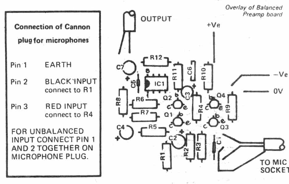 Typically the units aren't critical.
just the proportions are.
We are going to commence the justification by exploring the situation wherein input with R1 is at 0V and input with R4 is at + l00mV.
Typically the units aren't critical.
just the proportions are.
We are going to commence the justification by exploring the situation wherein input with R1 is at 0V and input with R4 is at + l00mV.
 Referring to Figure above, the revised board is very much similar to that of the original one, except some changes by removing some components along with the SIM.
The present on-board decoupling gives great performance.
It uses electrolytic of 100nF Polyester and 220uF electrolytic.
Alternatively, you can also use monolithic ceramic capacitor on every rail.
While C1 and C2 is referred as polarized electrolytic types, you may use non-polarized electros.
Another option would be to apply on C1 a 1uF polyester cap.
If C1 is intended to be used as tweeters you can use small values of 100nF which is good to go ahead.
If you are building the proposed simple 50 watt power amplifier circuit to use it for biamped/triamped system tweeter or midrange, the C1 valued need to be reduced to 100nF (3dB @ 72Hz).
Also you can use 1uF polyester at the rate of -3dB @ 7.2Hz in case of any general use.
However, this adjustment would increase the performance of the bass and you can also apply any value till 10uF (approx.) on C1 if needed to do so.
The new design of the PCB facilitates using the amp as dual-mono.
You can split the PCB track while each individual has its own power supply.
While the IMO carries less point, this enables cutting the PCB in half with each halves has its own supply.
The board gives the facility to make output connection to the PCB pins, or by using PCB mount spade lug.
Referring to Figure above, the revised board is very much similar to that of the original one, except some changes by removing some components along with the SIM.
The present on-board decoupling gives great performance.
It uses electrolytic of 100nF Polyester and 220uF electrolytic.
Alternatively, you can also use monolithic ceramic capacitor on every rail.
While C1 and C2 is referred as polarized electrolytic types, you may use non-polarized electros.
Another option would be to apply on C1 a 1uF polyester cap.
If C1 is intended to be used as tweeters you can use small values of 100nF which is good to go ahead.
If you are building the proposed simple 50 watt power amplifier circuit to use it for biamped/triamped system tweeter or midrange, the C1 valued need to be reduced to 100nF (3dB @ 72Hz).
Also you can use 1uF polyester at the rate of -3dB @ 7.2Hz in case of any general use.
However, this adjustment would increase the performance of the bass and you can also apply any value till 10uF (approx.) on C1 if needed to do so.
The new design of the PCB facilitates using the amp as dual-mono.
You can split the PCB track while each individual has its own power supply.
While the IMO carries less point, this enables cutting the PCB in half with each halves has its own supply.
The board gives the facility to make output connection to the PCB pins, or by using PCB mount spade lug.
 Figure above shows the IC pinouts for LM3876 where the pins are staggered to enable the PCB tracks run into the pin of the IC.
The LM3886 on the other hand is very much identical to the former, and it can be used by adding little more power, if needed.
However, the only difference that lies between the two is in LM3886 it is mandatory for Pin 5 to connect to +ve supply.
The PCB used for this amp is mainly meant for stereo amplifier.
It is single-sided with the location of supply fuse in the PCB.
The stereo board contain small four fuses (115mm x 40 mm).
Overall the revised board as in Figure 1.1 is of the same size to that of the original (as shown in Figure 1.0) and we have applied similar spacing in between the IC¡¯s to facilitate retro-fitting, if needed.
However, as a caution do keep in mind to use heat-sink for this project as the system gets really hot within a short time, which may end up destroying the things from overheating.
Figure above shows the IC pinouts for LM3876 where the pins are staggered to enable the PCB tracks run into the pin of the IC.
The LM3886 on the other hand is very much identical to the former, and it can be used by adding little more power, if needed.
However, the only difference that lies between the two is in LM3886 it is mandatory for Pin 5 to connect to +ve supply.
The PCB used for this amp is mainly meant for stereo amplifier.
It is single-sided with the location of supply fuse in the PCB.
The stereo board contain small four fuses (115mm x 40 mm).
Overall the revised board as in Figure 1.1 is of the same size to that of the original (as shown in Figure 1.0) and we have applied similar spacing in between the IC¡¯s to facilitate retro-fitting, if needed.
However, as a caution do keep in mind to use heat-sink for this project as the system gets really hot within a short time, which may end up destroying the things from overheating.
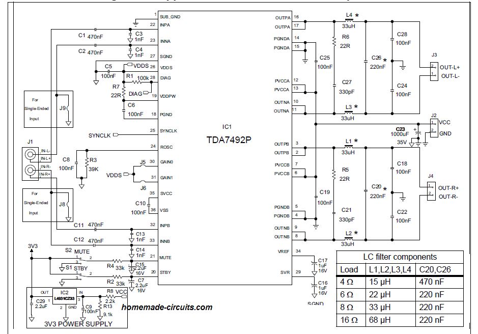
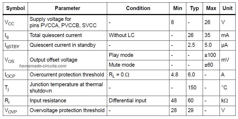
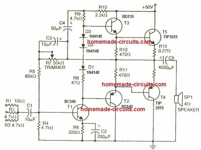 The 50 k preset helps to set the gain of the amplifier to the preferred limits.
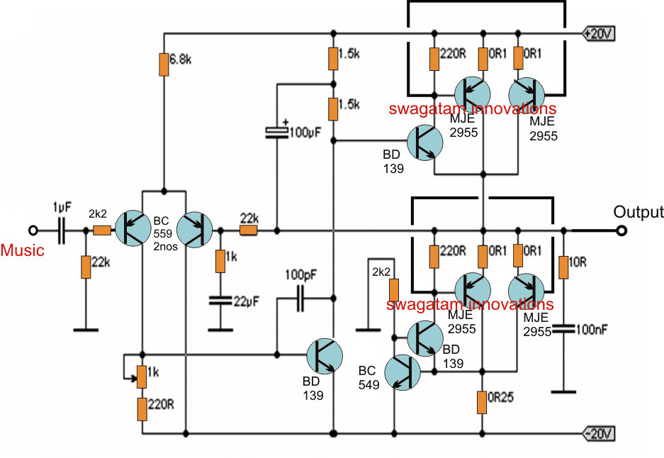
 This 20 watt amplifier circuit is a snap to construct and the majority of of the components is going to be accessible from your 'junk' box.
The design is made up of Darlington pre-diriver, Q1 and Q2, a VBE multiplier transistor Q3 and a quasi-complementary output stage comprising of transistors Q4-7.
All round shunt feedback loop is implemented through the Q7 collector to Q1's base by means of R3. this resistor R3 along with resistor R2, additionally offers DC feedback and input bias.
The voltage gain, and therefore the amplifier's level of sensitivity, is defined at 33 and 370mV through the ratio of the resistive divider R3 to R1.
The quiescent current by means of transistors Q5 and Q7 must be adjusted on 30mA using the preset PR1. R4 and R5 form the collector load of the Darlington transistor, which is bootstrapped by the capacitor C2 in order to supply a current drive for the output stage.
Despite the fact that great simplicity, the 20 watt amplifier has the ability to generate a good quality audio reproduction and can work pretty well using 4, 8 or 16 ohm load.
This 20 watt amplifier circuit is a snap to construct and the majority of of the components is going to be accessible from your 'junk' box.
The design is made up of Darlington pre-diriver, Q1 and Q2, a VBE multiplier transistor Q3 and a quasi-complementary output stage comprising of transistors Q4-7.
All round shunt feedback loop is implemented through the Q7 collector to Q1's base by means of R3. this resistor R3 along with resistor R2, additionally offers DC feedback and input bias.
The voltage gain, and therefore the amplifier's level of sensitivity, is defined at 33 and 370mV through the ratio of the resistive divider R3 to R1.
The quiescent current by means of transistors Q5 and Q7 must be adjusted on 30mA using the preset PR1. R4 and R5 form the collector load of the Darlington transistor, which is bootstrapped by the capacitor C2 in order to supply a current drive for the output stage.
Despite the fact that great simplicity, the 20 watt amplifier has the ability to generate a good quality audio reproduction and can work pretty well using 4, 8 or 16 ohm load.
 R5 delivers 100% negative feedback in the amplifier on DC to ensure that R1 to R3 enables you to bias the output with the suitable potential.
C6 and R4 decouple the feedback to some extent at audio frequencies and deliver a voltage gain of approximately 20 times (26dB).
This allows the circuit an input sensitivity of roughly 625mV RMS into 70k for an output power of 20 watts RMS.
R8 is employed to fix the most suitable quiescent current by means of the output transistors, which is around 80 to 100mA.
Power MOSFETs work in the negative coefficient mode, which means temperature compensation circuitry is never important for them.
R9 and C4 is configured like a low pass filter at the input of the circuit, which facilitates eliminating issues of RF interference.
C5 shifts the circuit a bit towards the high frequencies, assisting stability as well as serving to inhibit radio frequency vilnerability.
C3 and C8 are positioned as the input and output DC blocking capacitors respectively.
Applying a 50 volt DC supply with a load of an 8 ohm speaker, this amplifier circuit is able to deliver an output power of 20 watts RMS effortlessly.
An output power of approximately 15 watts RMS could be accomplished through a loaded supply voltage of approximately 40 volts roughly, and around 30 watts RMS might be reached employing a 60 volt DC input with an 8 ohm loaded speaker.
Despite the fact that the circuit might not be eligible for the super Hi-Fi class by existing specifications, it can produce an amazing degree of overall performance for a model of this sort of straightforwardness (it does, in fact, solely works with 4 transistors)! The overall harmonic distortion is usually effectively under 0.1% at nearly all output powers and frequencies, although it can increase somewhat at high and low output powers, and with high frequencies (as you could anticipate).
Although the BC177 transistor used for Tr1 is specified with a maximum emitter to collector voltage rating of only 45 volts, it really is protected to work with this device in this circuit using a supply of 50 V
R5 delivers 100% negative feedback in the amplifier on DC to ensure that R1 to R3 enables you to bias the output with the suitable potential.
C6 and R4 decouple the feedback to some extent at audio frequencies and deliver a voltage gain of approximately 20 times (26dB).
This allows the circuit an input sensitivity of roughly 625mV RMS into 70k for an output power of 20 watts RMS.
R8 is employed to fix the most suitable quiescent current by means of the output transistors, which is around 80 to 100mA.
Power MOSFETs work in the negative coefficient mode, which means temperature compensation circuitry is never important for them.
R9 and C4 is configured like a low pass filter at the input of the circuit, which facilitates eliminating issues of RF interference.
C5 shifts the circuit a bit towards the high frequencies, assisting stability as well as serving to inhibit radio frequency vilnerability.
C3 and C8 are positioned as the input and output DC blocking capacitors respectively.
Applying a 50 volt DC supply with a load of an 8 ohm speaker, this amplifier circuit is able to deliver an output power of 20 watts RMS effortlessly.
An output power of approximately 15 watts RMS could be accomplished through a loaded supply voltage of approximately 40 volts roughly, and around 30 watts RMS might be reached employing a 60 volt DC input with an 8 ohm loaded speaker.
Despite the fact that the circuit might not be eligible for the super Hi-Fi class by existing specifications, it can produce an amazing degree of overall performance for a model of this sort of straightforwardness (it does, in fact, solely works with 4 transistors)! The overall harmonic distortion is usually effectively under 0.1% at nearly all output powers and frequencies, although it can increase somewhat at high and low output powers, and with high frequencies (as you could anticipate).
Although the BC177 transistor used for Tr1 is specified with a maximum emitter to collector voltage rating of only 45 volts, it really is protected to work with this device in this circuit using a supply of 50 V
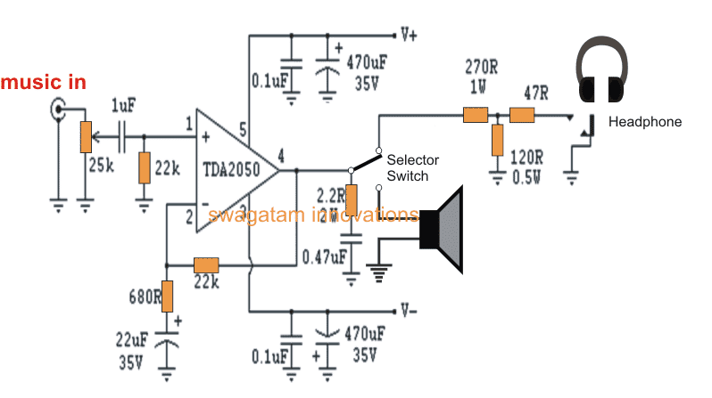
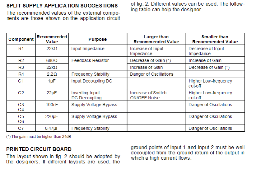
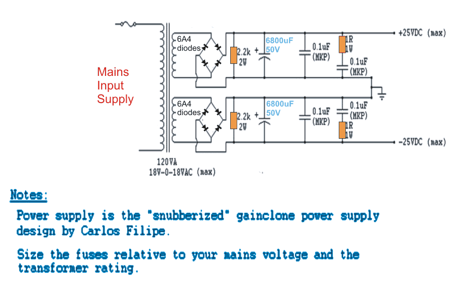
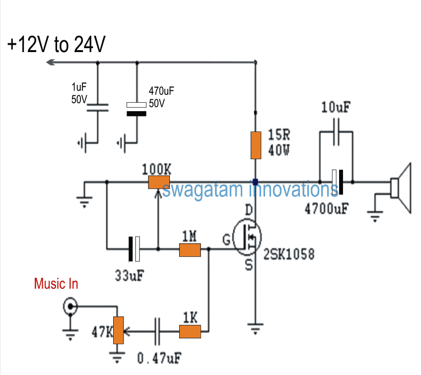
 The capacitors that we used in this experiment is that of Sprague.
This is used to couple the input and on the output a large electrolytic along with polyester bypass capacitor of 10¦ÌF.
To manage the load, we used four non-inductive wire wound resistors of 10W.
However, to achieve total resistance of 15 ohms, the resistors are wired on a series of two, which makes 30 ohms and furthermore setting up the sets in parallel.
Please note, the device would be hot and susceptible to burning during idle mode, hence caution is utmost important.
Class-A can never be an ideal option for a high efficiency amplifier design, but as we are applying the idea in this setup, we had to use more than 20 Watts power to generate a modest 4.8 Watts audio.
The heat-sink used for the mosfet was of 0.784 ¡ãC/W.
The capacitors that we used in this experiment is that of Sprague.
This is used to couple the input and on the output a large electrolytic along with polyester bypass capacitor of 10¦ÌF.
To manage the load, we used four non-inductive wire wound resistors of 10W.
However, to achieve total resistance of 15 ohms, the resistors are wired on a series of two, which makes 30 ohms and furthermore setting up the sets in parallel.
Please note, the device would be hot and susceptible to burning during idle mode, hence caution is utmost important.
Class-A can never be an ideal option for a high efficiency amplifier design, but as we are applying the idea in this setup, we had to use more than 20 Watts power to generate a modest 4.8 Watts audio.
The heat-sink used for the mosfet was of 0.784 ¡ãC/W.
 A 100K potentiometer (R3) along with a 1M fixed (R1) constitute a straightforward adjustable gate-bias circuit.
If we put a a voltmeter across the Q1 drain and the ground of the circuit, and we fine-tune R3 to get a meter reading of half the power supply voltage.
Practically any resistor could be utilized in place of R2 provided that the maximum current and power ratings of the FET aren't surpassed.
A resistor value of between 22 and 100 ohms can be a decent selection for testing.
If high current supply is used, make sure to use an appropriate heat sink for the FET.
A 100K potentiometer (R3) along with a 1M fixed (R1) constitute a straightforward adjustable gate-bias circuit.
If we put a a voltmeter across the Q1 drain and the ground of the circuit, and we fine-tune R3 to get a meter reading of half the power supply voltage.
Practically any resistor could be utilized in place of R2 provided that the maximum current and power ratings of the FET aren't surpassed.
A resistor value of between 22 and 100 ohms can be a decent selection for testing.
If high current supply is used, make sure to use an appropriate heat sink for the FET.
 When power output, harmonic, distortion, frequency response are not considered critical for an amplifier, for example in small radios receivers, applying a class 'A' amplifier becomes a favorable choice.
The circuit shown below makes use of just 3 transistors, is able to amplify with an output transformer, and provides an output power between 100 -200mW.
It operates using a battery supply as low as 4.5V.
RV1 works like a volume control and hooks up with the amplifier stage by means of C1. The below discussed three stages are directly connected.
The base bias of Q1 is implemented by resistors R2 and R5. Resistor R1 and transistor Q1 behave like a bias potential divider for Q2 base and likewise resistor R3 and transistor Q2 perform the bias base for the transistor Q3.
Resistor R2 and resistor R5 additionally work like a section of an overall negative feedback loop enhancing the frequency response of this BJT class A amplifier circuit, and also minimizing its distortion.
A bargain between gain and quality is determined through appropriate selection of R6 and C3 values.
C3 is configured like a decoupling capacitor and R6 value can be found through some experimentation.
(The lowest possible value of R6 should not be below 22k).
When power output, harmonic, distortion, frequency response are not considered critical for an amplifier, for example in small radios receivers, applying a class 'A' amplifier becomes a favorable choice.
The circuit shown below makes use of just 3 transistors, is able to amplify with an output transformer, and provides an output power between 100 -200mW.
It operates using a battery supply as low as 4.5V.
RV1 works like a volume control and hooks up with the amplifier stage by means of C1. The below discussed three stages are directly connected.
The base bias of Q1 is implemented by resistors R2 and R5. Resistor R1 and transistor Q1 behave like a bias potential divider for Q2 base and likewise resistor R3 and transistor Q2 perform the bias base for the transistor Q3.
Resistor R2 and resistor R5 additionally work like a section of an overall negative feedback loop enhancing the frequency response of this BJT class A amplifier circuit, and also minimizing its distortion.
A bargain between gain and quality is determined through appropriate selection of R6 and C3 values.
C3 is configured like a decoupling capacitor and R6 value can be found through some experimentation.
(The lowest possible value of R6 should not be below 22k).
 The circuit displayed above consists of a number of good features and is capable of providing a 5W of genuine class A audio into an 8 Ohm load.
Q1 and Q2, in conjunction with the connected parts, work like a top-notch voltage amplifier with all round ac and dc feedback fed from the Q2 collector by means of R6 to the Q1 emitter.
The output stage genuinely includes Q6 and Q7 configured like an emitter follower Darlington pair.
These transistors are driven by IC1, which is a 741 op amp.
These BJTs can be also seen incorporated in the 741's feedback loop.
These three elements together constitute a almost ideal output stage having an input impedance of many megohms along with a bandwidth ranging from a DC to higher than 100KHz.
Quiescent current is provided by The constant current source formed by the transistors Q3, Q4, Q5, R9 and R10 determine the quiscent current of the circuit.
The utilization of a constant current source in this class A amplifier design appropriately isolates the output stage from supply line fluctuations and ripple.
Using the indicated part values, the circuit gets a a bandwidth between 10Hz - 30KHz -3db, with a distortion much lower than 0.1% just before clipping.
The circuit also offers an input impedance of 1.5M and a sensitivity of 180mV for the complete output power.
Transistors Q4 to Q7 should be attached to an appropriate heatsink, which may have a dimension of 5" by 4" and should be finned type.
These heatsinks should be installed vertically and positioned in such a way that it gets exposed to adequate air flow.
The circuit displayed above consists of a number of good features and is capable of providing a 5W of genuine class A audio into an 8 Ohm load.
Q1 and Q2, in conjunction with the connected parts, work like a top-notch voltage amplifier with all round ac and dc feedback fed from the Q2 collector by means of R6 to the Q1 emitter.
The output stage genuinely includes Q6 and Q7 configured like an emitter follower Darlington pair.
These transistors are driven by IC1, which is a 741 op amp.
These BJTs can be also seen incorporated in the 741's feedback loop.
These three elements together constitute a almost ideal output stage having an input impedance of many megohms along with a bandwidth ranging from a DC to higher than 100KHz.
Quiescent current is provided by The constant current source formed by the transistors Q3, Q4, Q5, R9 and R10 determine the quiscent current of the circuit.
The utilization of a constant current source in this class A amplifier design appropriately isolates the output stage from supply line fluctuations and ripple.
Using the indicated part values, the circuit gets a a bandwidth between 10Hz - 30KHz -3db, with a distortion much lower than 0.1% just before clipping.
The circuit also offers an input impedance of 1.5M and a sensitivity of 180mV for the complete output power.
Transistors Q4 to Q7 should be attached to an appropriate heatsink, which may have a dimension of 5" by 4" and should be finned type.
These heatsinks should be installed vertically and positioned in such a way that it gets exposed to adequate air flow.
 The problem with class A amplifier circuits is their reduced efficiency in comparison to class B stages.
With this particular layout, and applying a 44 V power supply the quiescent current is going to be around 960 mA.
An output power of around 15 W is going to be supplied directly into an 8 Ohm loudspeaker.
Harmonic distortion can be expected to be lower than 0.1%.
The input sensitivity of ths design can be around 360 mV for with respect to power output, this can be around 15 W into 8 Ohm speaker.
The input impedance will be roughly 150 k.
For preamplifiers having a 1 k source impedance, capacitor C2 is going to be 6n8, for 2 k source impedance it will probably be 3n3. This class A amplifier provides a great feature of being short circuit proof; if you find a short it is going to consume roughly 1.6 A.
The potentiometer P10 is employed for implementing the offset control to the the no-signal output voltage at the intersection of the parts R18/R19 (around 21 V).
Every single output transistor (T6 and T7) must be mounted over a large heat sink, the thermal resistance must not be lower than 3.3¡ãC/W; driver transistors T4 and T5 will necessitate a clip type heatsink.
The problem with class A amplifier circuits is their reduced efficiency in comparison to class B stages.
With this particular layout, and applying a 44 V power supply the quiescent current is going to be around 960 mA.
An output power of around 15 W is going to be supplied directly into an 8 Ohm loudspeaker.
Harmonic distortion can be expected to be lower than 0.1%.
The input sensitivity of ths design can be around 360 mV for with respect to power output, this can be around 15 W into 8 Ohm speaker.
The input impedance will be roughly 150 k.
For preamplifiers having a 1 k source impedance, capacitor C2 is going to be 6n8, for 2 k source impedance it will probably be 3n3. This class A amplifier provides a great feature of being short circuit proof; if you find a short it is going to consume roughly 1.6 A.
The potentiometer P10 is employed for implementing the offset control to the the no-signal output voltage at the intersection of the parts R18/R19 (around 21 V).
Every single output transistor (T6 and T7) must be mounted over a large heat sink, the thermal resistance must not be lower than 3.3¡ãC/W; driver transistors T4 and T5 will necessitate a clip type heatsink.
 Q1 is utilized in the common emitter input stage and is linked directly to the output stage through the emitter follower buffer transistor, Q2. The latter is essential due to the output stage's rather large driving current.
The output transistor, Q5, is used in common emitter mode.
Its collector load is produced by Q3, Q4, and R7, and it is a constant current source.
The latter fixesthe circuit's output current to slightly below 1 amp.
The constant current generator load has a higher efficiency and linearity compared to an ordinaryload resistor.
At DC, R3 provides nearly 100 percent negative feedback to the amplifier, resulting in unity voltage gain.
R1 and R2 bias the input to 12 the supply voltage, which likewise biases the output to the desired level of 12 the supply voltage.
At audio frequencies, R5 and C3 eliminatessome of the feedback, allowing the circuit a maximum output sensitivity of around 380 mV rms.
C1 and C5 enable DC blocking at the input and output, correspondingly, while C2 and C4 help with stability.
Q4 and Q5 need to be placed atop a large heatsink.
Q1 is utilized in the common emitter input stage and is linked directly to the output stage through the emitter follower buffer transistor, Q2. The latter is essential due to the output stage's rather large driving current.
The output transistor, Q5, is used in common emitter mode.
Its collector load is produced by Q3, Q4, and R7, and it is a constant current source.
The latter fixesthe circuit's output current to slightly below 1 amp.
The constant current generator load has a higher efficiency and linearity compared to an ordinaryload resistor.
At DC, R3 provides nearly 100 percent negative feedback to the amplifier, resulting in unity voltage gain.
R1 and R2 bias the input to 12 the supply voltage, which likewise biases the output to the desired level of 12 the supply voltage.
At audio frequencies, R5 and C3 eliminatessome of the feedback, allowing the circuit a maximum output sensitivity of around 380 mV rms.
C1 and C5 enable DC blocking at the input and output, correspondingly, while C2 and C4 help with stability.
Q4 and Q5 need to be placed atop a large heatsink.

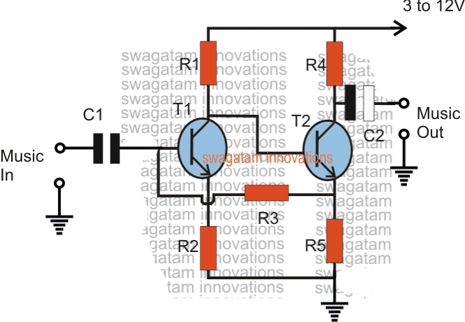 The circuit is a simple two transistor pre-amplifier using a feedback loop for enhancing the amplification.
Any music as we know is in the form of a consistently varying frequency, therefore when such a varying input is applied across the indicated C1 end terminals, the same is delivered across the base T1 and ground.
The higher amplitudes are processed normally and is reproduced with a potential that's approximately equal to the supply voltage, however for the lower misc amplitudes T2 is allowed to conduct at the higher ratio which is allowed to pass to its emitter.
At this time when the actual enhancement of the music is implemented by transferring this accumulated higher potential back to the base of T1 which correspondingly saturates at a much optimal rate.
This push pull action ultimately results in an overall amplification of an insignificantly small music or data input into a significantly larger output.
This simple circuit enables boosting extremely small or minimal frequencies to an appreciably bigger outputs which can be then used for feeding lager amplifiers.
The discussed circuit was actually popularly used in old cassette type playback recorders in their preamp stages for boosting the minute signals from the tape head so that the output from this small amplifier became compatible for the attached high power amplifier.
The circuit is a simple two transistor pre-amplifier using a feedback loop for enhancing the amplification.
Any music as we know is in the form of a consistently varying frequency, therefore when such a varying input is applied across the indicated C1 end terminals, the same is delivered across the base T1 and ground.
The higher amplitudes are processed normally and is reproduced with a potential that's approximately equal to the supply voltage, however for the lower misc amplitudes T2 is allowed to conduct at the higher ratio which is allowed to pass to its emitter.
At this time when the actual enhancement of the music is implemented by transferring this accumulated higher potential back to the base of T1 which correspondingly saturates at a much optimal rate.
This push pull action ultimately results in an overall amplification of an insignificantly small music or data input into a significantly larger output.
This simple circuit enables boosting extremely small or minimal frequencies to an appreciably bigger outputs which can be then used for feeding lager amplifiers.
The discussed circuit was actually popularly used in old cassette type playback recorders in their preamp stages for boosting the minute signals from the tape head so that the output from this small amplifier became compatible for the attached high power amplifier.
 The figure shows the circuit of the unit, and this is a straight Forward two transistor, direct coupled arrangement, with both transistors being used in the common emitter mode.
R2 provides local negative feedback over Tr1, and provides a convenient point tn which overall negative feedback can be applied to the circuit.
This feedback is obtained from the collector of Tr2 via D.C.
blocking capacitor C3 .
and the value of RF determines the amount of feedback that is applied to the amplier.
The lower the value of this component the more feedback that is applied, and the lower the closed loop voltage gain of the unit.
The required value of Rf is found by multiplying the required voltage gain by 560. Thus, a voltage gain of ten limes, for example, requires Rf to have a value of 5.6k.
It is recommended that the voltage gain should be kept within the limits stated earlier.
C2 rolls of the high frequency response of the amplier, and is necessary as instability might otherwise occur.
The upper -3dB response of the unit is still at about 200kHz even if the amplifier is used at a voltage gain of hundred times.
When used as lower gains the upper -3dB point is pushed proportionately higher.
The lower -3dB point is at approximately 20 Hertz incidentally.
The figure shows the circuit of the unit, and this is a straight Forward two transistor, direct coupled arrangement, with both transistors being used in the common emitter mode.
R2 provides local negative feedback over Tr1, and provides a convenient point tn which overall negative feedback can be applied to the circuit.
This feedback is obtained from the collector of Tr2 via D.C.
blocking capacitor C3 .
and the value of RF determines the amount of feedback that is applied to the amplier.
The lower the value of this component the more feedback that is applied, and the lower the closed loop voltage gain of the unit.
The required value of Rf is found by multiplying the required voltage gain by 560. Thus, a voltage gain of ten limes, for example, requires Rf to have a value of 5.6k.
It is recommended that the voltage gain should be kept within the limits stated earlier.
C2 rolls of the high frequency response of the amplier, and is necessary as instability might otherwise occur.
The upper -3dB response of the unit is still at about 200kHz even if the amplifier is used at a voltage gain of hundred times.
When used as lower gains the upper -3dB point is pushed proportionately higher.
The lower -3dB point is at approximately 20 Hertz incidentally.
 This is a high impedance input 2 stage preamplifier that features an adjustable voltage gain, from 1.5 to 10. This gain can be varied by setting up VRI and becomes handy where the MIC sensitivity required to be varied often.
As shown above, the circuit is actually designed for crystal microphones or ceramic cartridges.
This is a high impedance input 2 stage preamplifier that features an adjustable voltage gain, from 1.5 to 10. This gain can be varied by setting up VRI and becomes handy where the MIC sensitivity required to be varied often.
As shown above, the circuit is actually designed for crystal microphones or ceramic cartridges.
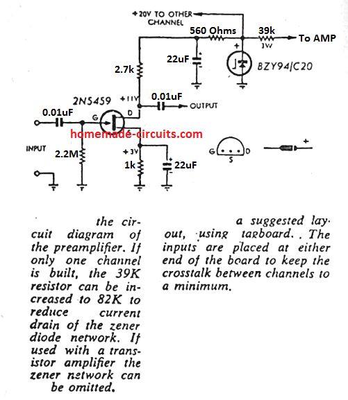
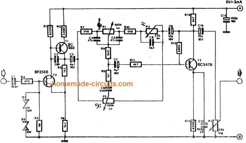 It usually becomes necessary to hook up an electric guitar with a mixing panel, a audio deck or a portable studio.
As much as wiring is concerned, that may be not an issue, however matching the high impedance of the guitar component with the low impedance of the line input of the mixing panel does becomes an issue.
Even the unsuspecting high impedance inputs of those units aren't well suited for the guitar output.
As soon as the guitar is plugged into this kind of input, you hardly see a signal feasible for the panel or deck to process.
It might be likely to attach the guitar to the (high-impedance) mic input, however that is commonly way too sensitive for the function, which leads to clipping of the guitar signal too easily.
The matching amplifier introduced in this article answers these difficulties: it features a high- impedance (1M) input that will stand up to voltages of over 200 V.
The output impedance is fairly small.
Amplication is X2 (6 dB).
Dual tone control, presence control and volume control are offered.
The circuit is designed for input levels of up to 3 V.
Over this level distortion rises, but that may be, naturally, a decent outcome having guitar music.
True clipping of the input signal is not going to take place until eventually significantly bigger levels above the minimum guitar specs are utilized.
The circuit is powered by a 9-V (PP3) battery through which the circuit pulls a current just around 3 mA.
It usually becomes necessary to hook up an electric guitar with a mixing panel, a audio deck or a portable studio.
As much as wiring is concerned, that may be not an issue, however matching the high impedance of the guitar component with the low impedance of the line input of the mixing panel does becomes an issue.
Even the unsuspecting high impedance inputs of those units aren't well suited for the guitar output.
As soon as the guitar is plugged into this kind of input, you hardly see a signal feasible for the panel or deck to process.
It might be likely to attach the guitar to the (high-impedance) mic input, however that is commonly way too sensitive for the function, which leads to clipping of the guitar signal too easily.
The matching amplifier introduced in this article answers these difficulties: it features a high- impedance (1M) input that will stand up to voltages of over 200 V.
The output impedance is fairly small.
Amplication is X2 (6 dB).
Dual tone control, presence control and volume control are offered.
The circuit is designed for input levels of up to 3 V.
Over this level distortion rises, but that may be, naturally, a decent outcome having guitar music.
True clipping of the input signal is not going to take place until eventually significantly bigger levels above the minimum guitar specs are utilized.
The circuit is powered by a 9-V (PP3) battery through which the circuit pulls a current just around 3 mA.
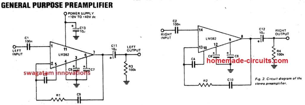 Here;s another nice little preamp circuit using a dual opamp IC LM382. Since the IC provides a dual opamp package two preamps could be created for stereo application.
The output from this preamp can be expected to be very good.
Parts List
R1, R2 = see the below given table.
R3, R4 = 100K 1/2 watt 5%
C1, C2 =100nF polyester
C3 to C10 = see table
C11 to C13 = 10uF/25V
IC1 = LM382
Here;s another nice little preamp circuit using a dual opamp IC LM382. Since the IC provides a dual opamp package two preamps could be created for stereo application.
The output from this preamp can be expected to be very good.
Parts List
R1, R2 = see the below given table.
R3, R4 = 100K 1/2 watt 5%
C1, C2 =100nF polyester
C3 to C10 = see table
C11 to C13 = 10uF/25V
IC1 = LM382
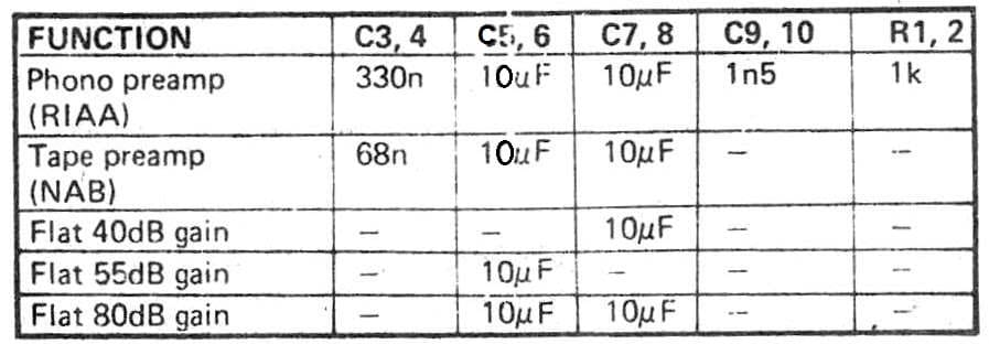
 UPDATE
Here are a couple of more preamplifier circuits that may interest you.
UPDATE
Here are a couple of more preamplifier circuits that may interest you.
 The circuit diagram is for a preamplier that can be employed with low impedance microphones, and should give an output signal of around 500mV.
R.M.S.
The prototype was found to work well with both 200 ohm and 600 ohm impedance dynamic microphones, but it should also work well with electret types which have a built-in FET buffer amplier, but no step-up transformer.
The unweighted noise performance of this circuit is not quite as good as that of the previous circuit, but is still about -60dB referred to 500mV R.M.S.
This circuit is really an adaptation of the second design.
The FET input stage uses the common gate mode rather than the common source one.
The common gate conguration gives reasonably good voltage gain together with a low input impedance (a few hundred ohms) which matches the micro- phone reasonably well.
The only other change in the circuit is that the emitter of Tr2 connects direct to the negative supply rail and there is no feedback resistor here.
This is done to boost the gain of the circuit, which as explained earlier, needs to be about ten times higher for a low impedance microphone.
The circuit diagram is for a preamplier that can be employed with low impedance microphones, and should give an output signal of around 500mV.
R.M.S.
The prototype was found to work well with both 200 ohm and 600 ohm impedance dynamic microphones, but it should also work well with electret types which have a built-in FET buffer amplier, but no step-up transformer.
The unweighted noise performance of this circuit is not quite as good as that of the previous circuit, but is still about -60dB referred to 500mV R.M.S.
This circuit is really an adaptation of the second design.
The FET input stage uses the common gate mode rather than the common source one.
The common gate conguration gives reasonably good voltage gain together with a low input impedance (a few hundred ohms) which matches the micro- phone reasonably well.
The only other change in the circuit is that the emitter of Tr2 connects direct to the negative supply rail and there is no feedback resistor here.
This is done to boost the gain of the circuit, which as explained earlier, needs to be about ten times higher for a low impedance microphone.
 R11 is = 6k8
The circuit demonstrated below provides a fundamental design concept, although not quite ideal, the final results to date are encouraging.
Applying even the highly sensitive measuring devices at our fingertips we still could not determine virtually any output noise signal whatsoever! Having said that, currently there seems to be still one leftover issue: the gain of the circuit is zero.
R11 is = 6k8
The circuit demonstrated below provides a fundamental design concept, although not quite ideal, the final results to date are encouraging.
Applying even the highly sensitive measuring devices at our fingertips we still could not determine virtually any output noise signal whatsoever! Having said that, currently there seems to be still one leftover issue: the gain of the circuit is zero.
 The specific signal amplifier stage is T2, which works in common emitter mode, the output signal being extracted from its collector.
A part of the output signal is supplied by means of emitter follower T3 towards a peak rectifier containing D1/D2 and C4. The voltage across C4 is employed to regulate the T1 base current, that constitutes section of the input attenuator.
At reduced signal concentrations the voltage on C4 is minimal, and T1 pulls very little current.
When the input signal level rises, the voltage on C4 goes up and T1 switches on harder, causing higher suppression of the input signal.
The overall effect is that as the input signal heightens it has to go through an increased degree of attenuation and the output signal thus continues to be reasonably constant across a wide range of input signals.
The circuit is appropriate for inputs having a peak input level up to 1 volt.
The microphone could be substituted by a tiny loudspeaker for converting the circuit into an intercom.
The specific signal amplifier stage is T2, which works in common emitter mode, the output signal being extracted from its collector.
A part of the output signal is supplied by means of emitter follower T3 towards a peak rectifier containing D1/D2 and C4. The voltage across C4 is employed to regulate the T1 base current, that constitutes section of the input attenuator.
At reduced signal concentrations the voltage on C4 is minimal, and T1 pulls very little current.
When the input signal level rises, the voltage on C4 goes up and T1 switches on harder, causing higher suppression of the input signal.
The overall effect is that as the input signal heightens it has to go through an increased degree of attenuation and the output signal thus continues to be reasonably constant across a wide range of input signals.
The circuit is appropriate for inputs having a peak input level up to 1 volt.
The microphone could be substituted by a tiny loudspeaker for converting the circuit into an intercom.
 The gain is roughly x 10 to x 20. If the signal source provides impedance of more than 100 k ohms, some amount of gain control is possible through P1. A reasonably long-term battery back up could be acquired through the use of a couple of 1.5 volt dry cells (in series) rather than one.
If the power falls under 1 volt the amplifier may stop functioning.
Typical dry cells frequently deplete quickly to 1 volt and have to subsequently be thrown away, although it may take longer for each one of two cells to drop to 0.5 volt.
Current draw at 3 volt supply will probably be around 450 microamps.
The gain is roughly x 10 to x 20. If the signal source provides impedance of more than 100 k ohms, some amount of gain control is possible through P1. A reasonably long-term battery back up could be acquired through the use of a couple of 1.5 volt dry cells (in series) rather than one.
If the power falls under 1 volt the amplifier may stop functioning.
Typical dry cells frequently deplete quickly to 1 volt and have to subsequently be thrown away, although it may take longer for each one of two cells to drop to 0.5 volt.
Current draw at 3 volt supply will probably be around 450 microamps.
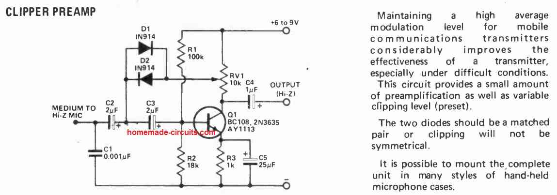
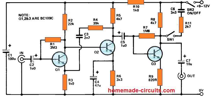 In addition, the midband voltage gain of the input stage is adjusted at around 46dB.
With that kind of a low input level, it is apparent that low noise transistors (such as the BC109C) are required to get excellent performance.
It additionallyhelps to operateQ1 witha low collector current, approximately 200uA.
Q3 serves as a low gain common emitter stage, providing extra amplification.
R9 adds negative feedback to adjust the voltage gain of Q3, and the given value yields a gain of around 14dB.
In addition, the midband voltage gain of the input stage is adjusted at around 46dB.
With that kind of a low input level, it is apparent that low noise transistors (such as the BC109C) are required to get excellent performance.
It additionallyhelps to operateQ1 witha low collector current, approximately 200uA.
Q3 serves as a low gain common emitter stage, providing extra amplification.
R9 adds negative feedback to adjust the voltage gain of Q3, and the given value yields a gain of around 14dB.

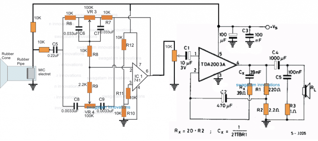
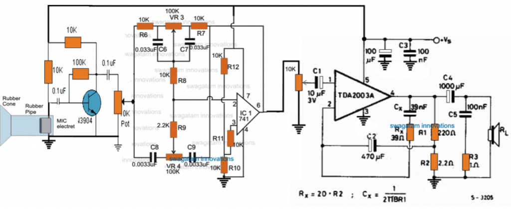 Jan:
Thank you for the update.
I have made the changes and must admit that it is much more sensitive, although I still cannot pick up a heartbeat clearly.
I think the problem might be with the microphone.
Question: Are all electret microphones more or less the same or do you get some that are more sensitive?
Analyzingthe Circuit Results
Thank you Jan,
Electret Mics are all similar with their specs according to me, they will behave identically unless the device is faulty or accidentally a duplicate low quality piece.
I think you will need to fine-tune the circuit for getting a proper optimal response from the output.For this first you must replace the speaker with a headphone so that the initial low un-optimized sound becomes slightly audible in our ears.
Once you get hold of the sound you can begin adjusting the bass treble pots until the most favorable sound becomes available in the headphones, later on once the audio is perfect the headphones can be replaced back with loudspeakers.
If you find the existing bass treble stage inadequate, you can replace it with the following 10 stage equalizer and get an access to a 10 level optimzation control.
https://www.homemade-circuits.com/2013/06/10-band-graphic-equalizer-circuit-for.html
Best Regards.
Warning: The concept has not been verified for its accuracy and credibility and the author does not in any manner endorse the use of this circuit for serious heart diagnosing.
Consult a qualified medical personal before using the explained circuit practically on a patient.
Jan:
Thank you for the update.
I have made the changes and must admit that it is much more sensitive, although I still cannot pick up a heartbeat clearly.
I think the problem might be with the microphone.
Question: Are all electret microphones more or less the same or do you get some that are more sensitive?
Analyzingthe Circuit Results
Thank you Jan,
Electret Mics are all similar with their specs according to me, they will behave identically unless the device is faulty or accidentally a duplicate low quality piece.
I think you will need to fine-tune the circuit for getting a proper optimal response from the output.For this first you must replace the speaker with a headphone so that the initial low un-optimized sound becomes slightly audible in our ears.
Once you get hold of the sound you can begin adjusting the bass treble pots until the most favorable sound becomes available in the headphones, later on once the audio is perfect the headphones can be replaced back with loudspeakers.
If you find the existing bass treble stage inadequate, you can replace it with the following 10 stage equalizer and get an access to a 10 level optimzation control.
https://www.homemade-circuits.com/2013/06/10-band-graphic-equalizer-circuit-for.html
Best Regards.
Warning: The concept has not been verified for its accuracy and credibility and the author does not in any manner endorse the use of this circuit for serious heart diagnosing.
Consult a qualified medical personal before using the explained circuit practically on a patient.
 C1 and C2 generate a bit of low frequency cut, lowering 50Hz pickup while the capacitors C4 and C5 alleviate problems with instability due to the circuit's high gain.
The output of the circuit must be hooked up to the input of an audio amplifier which must include a bass adjustment feature.
The bass pot must be adjusted to a high point for getting the best possible heartbeat sound response.
C1 and C2 generate a bit of low frequency cut, lowering 50Hz pickup while the capacitors C4 and C5 alleviate problems with instability due to the circuit's high gain.
The output of the circuit must be hooked up to the input of an audio amplifier which must include a bass adjustment feature.
The bass pot must be adjusted to a high point for getting the best possible heartbeat sound response.
 Fig:2
Fig:2
 Fig:3
Fig:3

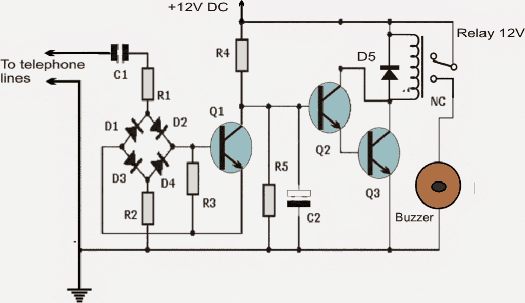
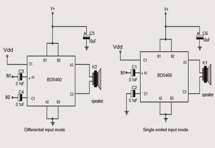 More info about the IC BD BD5460 may be acquired from the following datasheet of the IC.
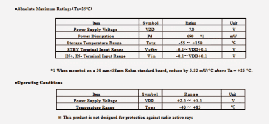
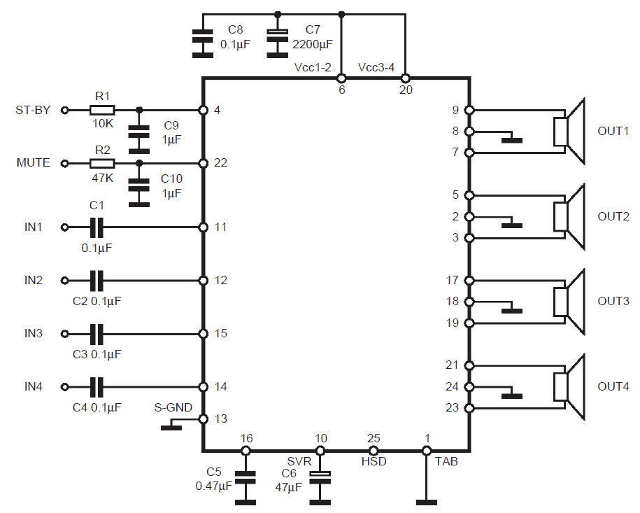
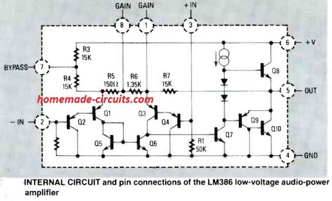
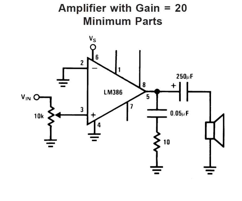 The input pin#2 goes to a 10K pot which becomes the volume control, one of its end terminals is picked forreceivingthe input signal while the other end is connected to ground, the center one goes to the hot end of the IC.
The speaker is connected to in #8 via a high value blocking capacitor, the resistor/capacitor arrangement connected across pin #5 and ground has beenincludedfor frequency compensation and to provide greater stability to the circuit.
The next circuit shows asimilardesign as above, except that its pins 1 and 8 have been connected to a capacitor of 10uF, which as explained above helps to pull the gain of the amplifier to 200
The input pin#2 goes to a 10K pot which becomes the volume control, one of its end terminals is picked forreceivingthe input signal while the other end is connected to ground, the center one goes to the hot end of the IC.
The speaker is connected to in #8 via a high value blocking capacitor, the resistor/capacitor arrangement connected across pin #5 and ground has beenincludedfor frequency compensation and to provide greater stability to the circuit.
The next circuit shows asimilardesign as above, except that its pins 1 and 8 have been connected to a capacitor of 10uF, which as explained above helps to pull the gain of the amplifier to 200
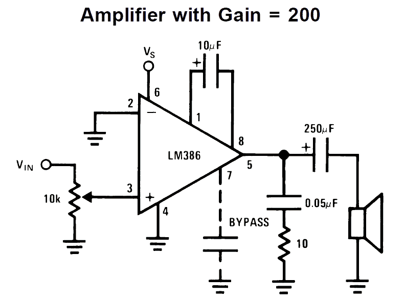
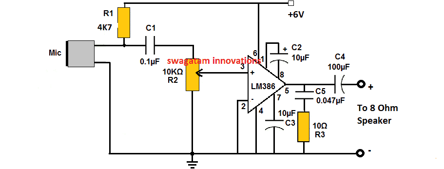 The following image shows how the above explained LM386 may be applied for achieving a simple yet powerful microphone amplifier circuit as shown below
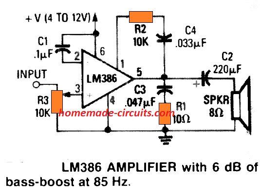 So far we know that attaching a 10-¦ÌF electrolytic across pins 1 and 8, it is possible to enhance the actual gain of the circuit to 200. This happens due to the capacitor appropriately shorting out the IC's in-built 1.35K resistor.
The figure above illustrates the way to shunt that resistor by implementing C4 -R2, to allow 6 -dB of bass boost at 85 Hz.
This compensates the actual inability of the chip to produce suitable bass effect through typically used low-cost 8 ohm speakers.
So far we know that attaching a 10-¦ÌF electrolytic across pins 1 and 8, it is possible to enhance the actual gain of the circuit to 200. This happens due to the capacitor appropriately shorting out the IC's in-built 1.35K resistor.
The figure above illustrates the way to shunt that resistor by implementing C4 -R2, to allow 6 -dB of bass boost at 85 Hz.
This compensates the actual inability of the chip to produce suitable bass effect through typically used low-cost 8 ohm speakers.
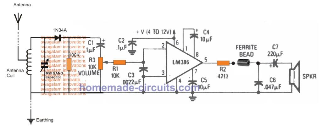 The figure above shows how the LM386 amplifier design could be customized like a compact amplifier for making a simple AM radio.
Here, the detected AM transmission is supplied to the non-inverting input of the IC through volume control pot R3, and the resulting RF is de-coupled by way of R1, C3.
Any sort of left over RF disturbances are blocked from passing on to the loudspeaker through the indicated ferrite bead.
In this LM386 AM radio design, the voltage gain of the IC is set at 200 through C4. You can also see that the circuit is supplied through supplemental power supply ripple rejection stage by configuring C5 between pin 7 and the negative line.
The figure above shows how the LM386 amplifier design could be customized like a compact amplifier for making a simple AM radio.
Here, the detected AM transmission is supplied to the non-inverting input of the IC through volume control pot R3, and the resulting RF is de-coupled by way of R1, C3.
Any sort of left over RF disturbances are blocked from passing on to the loudspeaker through the indicated ferrite bead.
In this LM386 AM radio design, the voltage gain of the IC is set at 200 through C4. You can also see that the circuit is supplied through supplemental power supply ripple rejection stage by configuring C5 between pin 7 and the negative line.
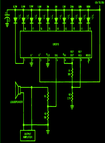
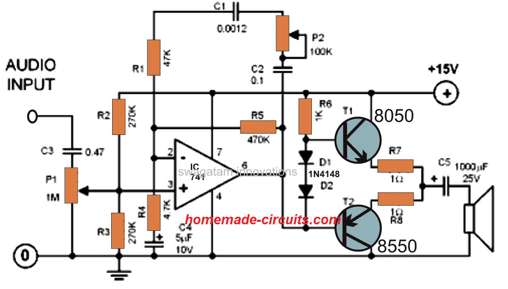
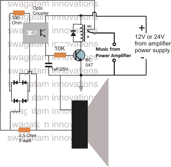 The next simple short circuit and overload protector design presented here can be used for protecting valuable mains operated gadgets like amplifiers, TV sets, DVD players or any other similar appliance.
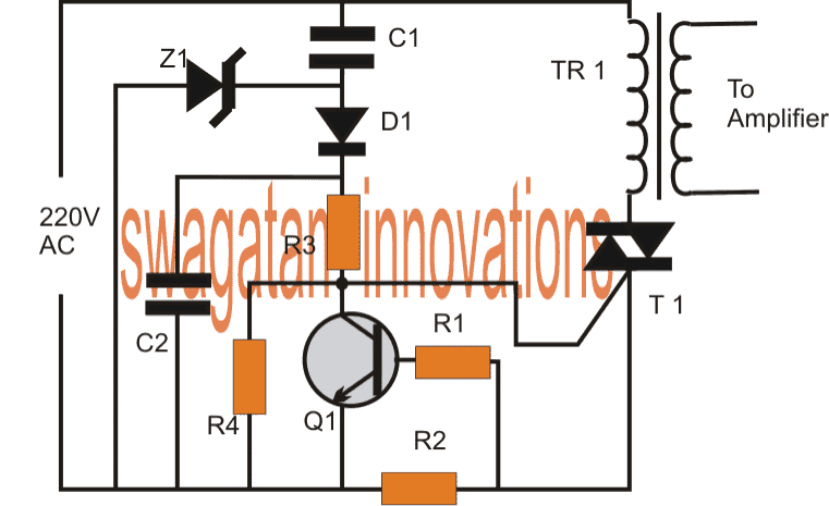
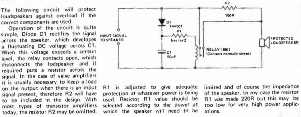
 I have modified the above design by adding a couple of 1N4148 diodes in place of the preset.
This gets rid of the preset adjustments and allows the user to directly switch ON the amp with a speaker connected.
I have modified the above design by adding a couple of 1N4148 diodes in place of the preset.
This gets rid of the preset adjustments and allows the user to directly switch ON the amp with a speaker connected.
 Circuit Diagram with Magnified Part Values

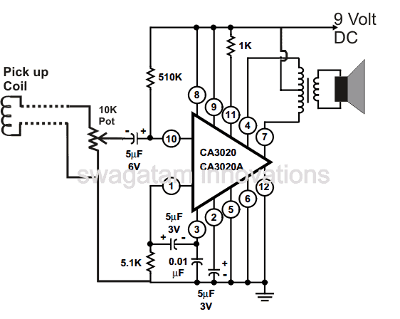
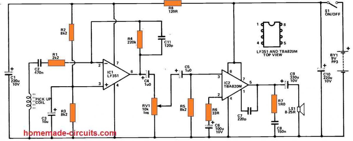 It is feasible to utilize an evensimpler circuit in casea direct connection to the telephone is established.
However,this would complicate setup and this maybeILLEGAL to createa direct connection to a telephone in any case.
The unit's preamplifier stage is based on IC1, which is a low noise op amp with a FET input stage.
This is utilized in the usual inverting audio amplifier configuration, and the negative feedback circuit, R1, 4, adjusts the voltage gain to around 40dB.
(100 times).
C11 lowers the gain somewhat at higher frequency to enhance the signal-to-noise ratio.
C4 connects the preamplifier output to volume control, RV1, and C5 connects the signal to the power amplifier.
The output stage employs the TBA820M, a class B amplifier withsomehundredmilliwatts rms of output power.
The device's closed loop voltage gain is governed by the R6 value, which is approximately 25dB.
(180 times) with the stated value.
This provides the needed extremely large overall gain in combination with the gain of the preamplifier.
C7, R7, and C8 are required to sustain stability.
The unit's quiescent current specificationisapproximately 5mA, although it can reach 50mA or more at high volume levels.
With a little trial and error, the optimal placement for the pick-up coil on the telephone pedestal (not really the handset) may be determined.
It is feasible to utilize an evensimpler circuit in casea direct connection to the telephone is established.
However,this would complicate setup and this maybeILLEGAL to createa direct connection to a telephone in any case.
The unit's preamplifier stage is based on IC1, which is a low noise op amp with a FET input stage.
This is utilized in the usual inverting audio amplifier configuration, and the negative feedback circuit, R1, 4, adjusts the voltage gain to around 40dB.
(100 times).
C11 lowers the gain somewhat at higher frequency to enhance the signal-to-noise ratio.
C4 connects the preamplifier output to volume control, RV1, and C5 connects the signal to the power amplifier.
The output stage employs the TBA820M, a class B amplifier withsomehundredmilliwatts rms of output power.
The device's closed loop voltage gain is governed by the R6 value, which is approximately 25dB.
(180 times) with the stated value.
This provides the needed extremely large overall gain in combination with the gain of the preamplifier.
C7, R7, and C8 are required to sustain stability.
The unit's quiescent current specificationisapproximately 5mA, although it can reach 50mA or more at high volume levels.
With a little trial and error, the optimal placement for the pick-up coil on the telephone pedestal (not really the handset) may be determined.
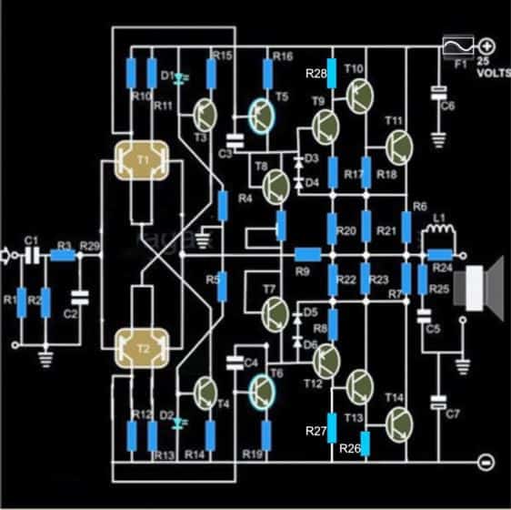
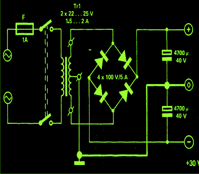
 TheMosfet version of the above design can be witnessedin the below given image:
 For the complete construction details, please refer to the following link:
Mini Crescendo pdf with PCB and protection circuitsVideo of the Crescendo Amplifier showing the PCB Design and the Component Layout Details,along with the Complete Test Report:
Contributed by Mr.
Siva
For the complete construction details, please refer to the following link:
Mini Crescendo pdf with PCB and protection circuitsVideo of the Crescendo Amplifier showing the PCB Design and the Component Layout Details,along with the Complete Test Report:
Contributed by Mr.
Siva
 An alternate version of the above explained 250 watt power amplifier can eb seen in the following diagram having all the details regarding the components:
 In every vehicle the fuel tank is probably the most important part of the entire system, since the vehicle's operation critically depends on the presence of the tank fuel.
This also means that monitoring the fuel level in the tank becomes an essential factor for the owner or the driver of the vehicle.
Although, most vehicles are already equipped with an advanced digital fuel sensor indicator device, building your own circuit can be a lot of fun and satisfaction.
Warning: This project is only for experimental purpose.
It must be done under expert supervision, if actual fuel is used for the tank fluid.
In this article we will learn how to build an LED based fuel indicator circuit using GSM wireless ultrasonic sensors and Arduino.
In every vehicle the fuel tank is probably the most important part of the entire system, since the vehicle's operation critically depends on the presence of the tank fuel.
This also means that monitoring the fuel level in the tank becomes an essential factor for the owner or the driver of the vehicle.
Although, most vehicles are already equipped with an advanced digital fuel sensor indicator device, building your own circuit can be a lot of fun and satisfaction.
Warning: This project is only for experimental purpose.
It must be done under expert supervision, if actual fuel is used for the tank fluid.
In this article we will learn how to build an LED based fuel indicator circuit using GSM wireless ultrasonic sensors and Arduino.
 The ultrasonic sensor will need to be installed by inserting the sensing heads through perfectly dimensioned holes, and sealed with appropriate sealing agent.
We can see the tank is specified with two measures, one is the full height, and the other is the maximum or the optimal fuel height inside the tank.
You will have to note these two measures as these will be required to be entered in the program code for the Arduino.
The ultrasonic sensor will need to be installed by inserting the sensing heads through perfectly dimensioned holes, and sealed with appropriate sealing agent.
We can see the tank is specified with two measures, one is the full height, and the other is the maximum or the optimal fuel height inside the tank.
You will have to note these two measures as these will be required to be entered in the program code for the Arduino.
 Here, the nRF24L01 wireless works like a receiver.
The antenna captures the RF content transmitted by the transmitter circuit, and sends it to the Arduino.
As per the program code, the Arduino analyzes the varying ultrasonic time, and translates it into an incrementing digital output.
This digital output which corresponds with the instantaneous height or the level of the fuel is fed into an LED array.
The LEDs in the array respond and illuminate sequentially enabling a direct visual indication of the fuel level to the owner.
The green LEDs indicate a healthy condition of the fuel content.
The yellow LED indicates that the vehicle needs a refueling quickly, while the red LED indicates a critical situation, regarding the fuel about to finish.
The buzzer now starts buzzing creating the necessary warning alarm.
Here, the nRF24L01 wireless works like a receiver.
The antenna captures the RF content transmitted by the transmitter circuit, and sends it to the Arduino.
As per the program code, the Arduino analyzes the varying ultrasonic time, and translates it into an incrementing digital output.
This digital output which corresponds with the instantaneous height or the level of the fuel is fed into an LED array.
The LEDs in the array respond and illuminate sequentially enabling a direct visual indication of the fuel level to the owner.
The green LEDs indicate a healthy condition of the fuel content.
The yellow LED indicates that the vehicle needs a refueling quickly, while the red LED indicates a critical situation, regarding the fuel about to finish.
The buzzer now starts buzzing creating the necessary warning alarm.
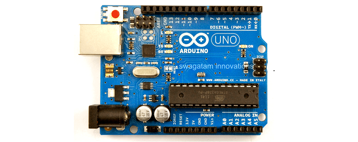
 Processor: ATMEGA4809, NINA-W132 Wi-Fi module from u-blox, ECC608 crypto device
Frequency: 16 MHz
Format: Arduino / Genuino
Size: 68.6 mm x 53.4 mm
Host interface: USB/32U4
Voltage: 5 V
Flash: 48 KB
EEPROM: None
SRAM: 0.25 KB
Digital I/O Pins: 6 (14 are PWM based)
Analogue Input: 5
Analogue Output: 6
Miscellaneous: Comes with 6-axis accelerometer, gyroscope the NINA/esp32 module works with WiFi and Bluetooth
Processor: ATMEGA4809, NINA-W132 Wi-Fi module from u-blox, ECC608 crypto device
Frequency: 16 MHz
Format: Arduino / Genuino
Size: 68.6 mm x 53.4 mm
Host interface: USB/32U4
Voltage: 5 V
Flash: 48 KB
EEPROM: None
SRAM: 0.25 KB
Digital I/O Pins: 6 (14 are PWM based)
Analogue Input: 5
Analogue Output: 6
Miscellaneous: Comes with 6-axis accelerometer, gyroscope the NINA/esp32 module works with WiFi and Bluetooth
 Processor: ATSAMW25 (using SAMD21 Cortex-M0+ 32 bit ARM MCU, WINC1500 2.4GHz 802.11 b/g/n Wi-Fi, and ECC508 crypto device )
Frequency: 48 MHz
Format: Minimal
Size: 61.5mm ¡Á25mm
Host interface: USB
Voltage: 3.3 V
Flash: 256 KB
EEPROM: None
SRAM: 32 KB
Digital I/O Pins: 8 (12 are PWM based)
Analogue Input: 7
Analogue Output: 1
Processor: ATSAMW25 (using SAMD21 Cortex-M0+ 32 bit ARM MCU, WINC1500 2.4GHz 802.11 b/g/n Wi-Fi, and ECC508 crypto device )
Frequency: 48 MHz
Format: Minimal
Size: 61.5mm ¡Á25mm
Host interface: USB
Voltage: 3.3 V
Flash: 256 KB
EEPROM: None
SRAM: 32 KB
Digital I/O Pins: 8 (12 are PWM based)
Analogue Input: 7
Analogue Output: 1
 Processor: Intel Curie module2 tiny cores, one x86 (Quark SE) along with ARC
Frequency: 32 MHz
Format: Arduino / Genuino
Size: 68.6mm ¡Á53.4mm
Host interface: USB
Voltage: 3.3 V
Flash: 196 KB
EEPROM: N/A
SRAM: 24 KB
Digital I/O Pins: 14 (4 are PWM based)
Analogue Input: 6
Analogue Output: N/A
Miscellaneous: Includes 6-axis accelerometer, gyroscope and Bluetooth
Processor: Intel Curie module2 tiny cores, one x86 (Quark SE) along with ARC
Frequency: 32 MHz
Format: Arduino / Genuino
Size: 68.6mm ¡Á53.4mm
Host interface: USB
Voltage: 3.3 V
Flash: 196 KB
EEPROM: N/A
SRAM: 24 KB
Digital I/O Pins: 14 (4 are PWM based)
Analogue Input: 6
Analogue Output: N/A
Miscellaneous: Includes 6-axis accelerometer, gyroscope and Bluetooth
 Processor: ATSAMD21G18A
Frequency: 48 MHz
Format: Arduino
Size: 68.6mm ¡Á53.3mm
Host interface: USB
Voltage: 3.3 V
Flash: 256 KB
EEPROM: 0-16 Kb emulation
SRAM: 32 KB
Digital I/O Pins: 14 (12 are PWM based)
Analogue Input: 6
Analogue Output: 1
Miscellaneous: 32-bit architecture
Processor: ATSAMD21G18A
Frequency: 48 MHz
Format: Arduino
Size: 68.6mm ¡Á53.3mm
Host interface: USB
Voltage: 3.3 V
Flash: 256 KB
EEPROM: 0-16 Kb emulation
SRAM: 32 KB
Digital I/O Pins: 14 (12 are PWM based)
Analogue Input: 6
Analogue Output: 1
Miscellaneous: 32-bit architecture
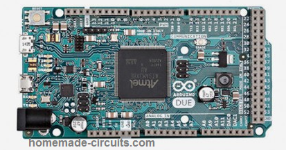 Processor: ATSAM3X8E
Frequency: 84 MHz
Format: Mega
Size: 101.6mm ¡Á53.3mm
Host interface: 16U2+ native host
Voltage: 3.3 V
Flash: 512 KB
EEPROM: 0
SRAM: 96 KB
Digital I/O Pins: 54 (12 are PWM based)
Analogue Input: 12
Analogue Output: 2
Miscellaneous: It is the first Arduino board built withARMProcessor.
In contrast to most Arduino boards, it can be used only with 3.3V and not 5V.
Processor: ATSAM3X8E
Frequency: 84 MHz
Format: Mega
Size: 101.6mm ¡Á53.3mm
Host interface: 16U2+ native host
Voltage: 3.3 V
Flash: 512 KB
EEPROM: 0
SRAM: 96 KB
Digital I/O Pins: 54 (12 are PWM based)
Analogue Input: 12
Analogue Output: 2
Miscellaneous: It is the first Arduino board built withARMProcessor.
In contrast to most Arduino boards, it can be used only with 3.3V and not 5V.
 Processor: Atmega32U4, Atheros AR9331
Frequency: 16MHz, 400MHz
Format: Arduino
Size: 68.6mm ¡Á53.3mm
Host interface: USB
Voltage: 5 V
Flash: 32 KB, 16 MB
EEPROM: 1 KB, 0 KB
SRAM: 2.5 KB, 64 MB
Digital I/O Pins: 14 (6 are PWM based)
Analogue Input: 12
Analogue Output: N/A
Miscellaneous: Arduino Y¨²n is a blend of a classic Arduino Leonardo (built around the Atmega32U4 processor) includes an on chip WiFisystem (SoC) operating Linino, aMIPSGNU/Linux based onOpenWrt.
Processor: Atmega32U4, Atheros AR9331
Frequency: 16MHz, 400MHz
Format: Arduino
Size: 68.6mm ¡Á53.3mm
Host interface: USB
Voltage: 5 V
Flash: 32 KB, 16 MB
EEPROM: 1 KB, 0 KB
SRAM: 2.5 KB, 64 MB
Digital I/O Pins: 14 (6 are PWM based)
Analogue Input: 12
Analogue Output: N/A
Miscellaneous: Arduino Y¨²n is a blend of a classic Arduino Leonardo (built around the Atmega32U4 processor) includes an on chip WiFisystem (SoC) operating Linino, aMIPSGNU/Linux based onOpenWrt.
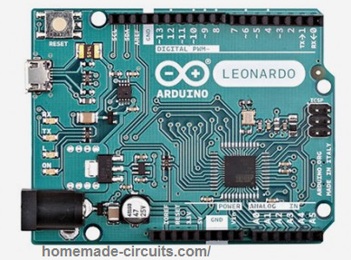 Processor: Atmega32U4
Frequency: 16MHz
Format: Arduino
Size: 68.6mm ¡Á53.3mm
Host interface: USB/32U4
Voltage: 5 V
Flash: 32 KB
EEPROM: 1 KB
SRAM: 2.5 KB
Digital I/O Pins: 20 (7 are PWM based)
Analogue Input: 12
Analogue Output: N/A
Miscellaneous: The Leonardo is designed with the Atmega32U4 processor, which features an integrated USB controller, which reduces a single chip as compared to other Arduino versions.
Processor: Atmega32U4
Frequency: 16MHz
Format: Arduino
Size: 68.6mm ¡Á53.3mm
Host interface: USB/32U4
Voltage: 5 V
Flash: 32 KB
EEPROM: 1 KB
SRAM: 2.5 KB
Digital I/O Pins: 20 (7 are PWM based)
Analogue Input: 12
Analogue Output: N/A
Miscellaneous: The Leonardo is designed with the Atmega32U4 processor, which features an integrated USB controller, which reduces a single chip as compared to other Arduino versions.
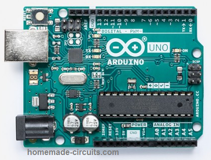 Processor: ATmega328P
Frequency: 16MHz
Format: Arduino
Size: 68.6mm ¡Á53.3mm
Host interface: USB/8U2(Rev1&2)/16U2(Rev3)
Voltage: 5 V
Flash: 32 KB
EEPROM: 1 KB
SRAM: 2 KB
Digital I/O Pins: 2 (14 are PWM based)
Analogue Input: 6
Analogue Output: 6
Miscellaneous: This works with the very same ATmega328 as late-model Duemilanove, but while the Duemilanove incorporated anFTDIIC for USB, the Uno operates with an ATmega16U2 (ATmega8U2 before rev3) programmed as a serial converter.
Processor: ATmega328P
Frequency: 16MHz
Format: Arduino
Size: 68.6mm ¡Á53.3mm
Host interface: USB/8U2(Rev1&2)/16U2(Rev3)
Voltage: 5 V
Flash: 32 KB
EEPROM: 1 KB
SRAM: 2 KB
Digital I/O Pins: 2 (14 are PWM based)
Analogue Input: 6
Analogue Output: 6
Miscellaneous: This works with the very same ATmega328 as late-model Duemilanove, but while the Duemilanove incorporated anFTDIIC for USB, the Uno operates with an ATmega16U2 (ATmega8U2 before rev3) programmed as a serial converter.
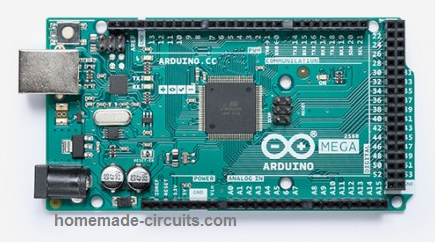 Processor: ATmega2560
Frequency: 16MHz
Format: Mega
Size: 101.6mm ¡Á53.3mm
Host interface: USB/8U2(Rev1&2)/16U2(Rev3)
Voltage: 5 V
Flash: 256 KB
EEPROM: 4 KB
SRAM: 8 KB
Digital I/O Pins: 54 (15 are PWM based)
Analogue Input: 16
Analogue Output: N/A
Miscellaneous: The majority of the shielding that had been created for the Duemilanove, Diecimila, or Uno will have no problems here, however some shields may not accommodate due to of incompatibility with the supplemental pins.
Processor: ATmega2560
Frequency: 16MHz
Format: Mega
Size: 101.6mm ¡Á53.3mm
Host interface: USB/8U2(Rev1&2)/16U2(Rev3)
Voltage: 5 V
Flash: 256 KB
EEPROM: 4 KB
SRAM: 8 KB
Digital I/O Pins: 54 (15 are PWM based)
Analogue Input: 16
Analogue Output: N/A
Miscellaneous: The majority of the shielding that had been created for the Duemilanove, Diecimila, or Uno will have no problems here, however some shields may not accommodate due to of incompatibility with the supplemental pins.
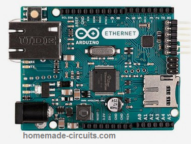 Processor: ATmega328
Frequency: 16MHz
Format: Mega
Size: 101.6mm ¡Á53.3mm
Host interface: Ethernet Serial interface, Wiznet Ethernet
Voltage: 5 V
Flash: 32 KB
EEPROM: 1 KB
SRAM: 2 KB
Digital I/O Pins: 14 (4 are PWM based)
Analogue Input: 6
Analogue Output: N/A
Miscellaneous: Structured around the same WIZnet W5100 chip as the Arduino Ethernet Shield.A serial interface has been included for programming, but it lacks USB port.
Newer versions of this board are compatible withPower over Ethernet(PoE).
Processor: ATmega328
Frequency: 16MHz
Format: Mega
Size: 101.6mm ¡Á53.3mm
Host interface: Ethernet Serial interface, Wiznet Ethernet
Voltage: 5 V
Flash: 32 KB
EEPROM: 1 KB
SRAM: 2 KB
Digital I/O Pins: 14 (4 are PWM based)
Analogue Input: 6
Analogue Output: N/A
Miscellaneous: Structured around the same WIZnet W5100 chip as the Arduino Ethernet Shield.A serial interface has been included for programming, but it lacks USB port.
Newer versions of this board are compatible withPower over Ethernet(PoE).
 Processor: ATmega328P
Frequency: 8MHz
Format: minimal
Size: 66.0mm ¡Á27.9mm
Host interface: XBeeSerial
Voltage: 3.3 V
Flash: 32 KB
EEPROM: 1 KB
SRAM: 2 KB
Digital I/O Pins: 14 (6 are PWM based)
Analogue Input: 8
Analogue Output: N/A
Miscellaneous: XBeesocket can be found at the bottom portion of the board
Processor: ATmega328P
Frequency: 8MHz
Format: minimal
Size: 66.0mm ¡Á27.9mm
Host interface: XBeeSerial
Voltage: 3.3 V
Flash: 32 KB
EEPROM: 1 KB
SRAM: 2 KB
Digital I/O Pins: 14 (6 are PWM based)
Analogue Input: 8
Analogue Output: N/A
Miscellaneous: XBeesocket can be found at the bottom portion of the board
 Processor: ATmega328 (ATmega168 before v3.0)
Frequency: 16MHz
Format: minimal
Size: 43.18mm ¡Á18.54mm
Host interface: USB/ FTDIFT232R
Voltage: 5 V
Flash: 16/32 KB
EEPROM: 0.5/1 KB
SRAM: 1/2 KB
Digital I/O Pins: 14 (6 are PWM based)
Analogue Input: 8
Analogue Output: N/A
Miscellaneous: This is a tiny version of the Arduino that works with USB power and is built with a surface-mounted processor.
Processor: ATmega328 (ATmega168 before v3.0)
Frequency: 16MHz
Format: minimal
Size: 43.18mm ¡Á18.54mm
Host interface: USB/ FTDIFT232R
Voltage: 5 V
Flash: 16/32 KB
EEPROM: 0.5/1 KB
SRAM: 1/2 KB
Digital I/O Pins: 14 (6 are PWM based)
Analogue Input: 8
Analogue Output: N/A
Miscellaneous: This is a tiny version of the Arduino that works with USB power and is built with a surface-mounted processor.
 Processor: ATmega168V or ATmega328V
Frequency: 8MHz
Format: wearable
Size: 51mm[2in]
Host interface: USB/ FTDIFT232R
Voltage: 2.7-5.5V
Flash: 16 KB
EEPROM: 0.5 KB
SRAM: 1 KB
Digital I/O Pins: 14 (6 are PWM based)
Analogue Input: 6
Analogue Output: N/A
Miscellaneous: Comes with bare minimum features and designed forwearable applications.
Processor: ATmega168V or ATmega328V
Frequency: 8MHz
Format: wearable
Size: 51mm[2in]
Host interface: USB/ FTDIFT232R
Voltage: 2.7-5.5V
Flash: 16 KB
EEPROM: 0.5 KB
SRAM: 1 KB
Digital I/O Pins: 14 (6 are PWM based)
Analogue Input: 6
Analogue Output: N/A
Miscellaneous: Comes with bare minimum features and designed forwearable applications.
 Processor: ATmega168V or ATmega328V
Frequency: 16MHz
Format: Arduino
Size: 52.1mm ¡Á53.3mm
Host interface: UARTSerial, I2C(TWI), SPIFTDI
Voltage: 5V or 3.3V
Flash: 16/32 KB
EEPROM: 0.5/1 KB
SRAM: 1/2 KB
Digital I/O Pins: 14 (6 are PWM based)
Analogue Input: 6
Analogue Output: N/A
Miscellaneous: Manufactured bySparkFun Electronicsfor use in temporary installations.
Processor: ATmega168V or ATmega328V
Frequency: 16MHz
Format: Arduino
Size: 52.1mm ¡Á53.3mm
Host interface: UARTSerial, I2C(TWI), SPIFTDI
Voltage: 5V or 3.3V
Flash: 16/32 KB
EEPROM: 0.5/1 KB
SRAM: 1/2 KB
Digital I/O Pins: 14 (6 are PWM based)
Analogue Input: 6
Analogue Output: N/A
Miscellaneous: Manufactured bySparkFun Electronicsfor use in temporary installations.
 Processor: ATmega2560
Frequency: 16MHz
Format: Mega
Size: 101.6mm ¡Á53.3mm
Host interface: 8U2, MAX3421E,USB Host
Voltage: 5V
Flash: 256 KB
EEPROM: 4 KB
SRAM: 8 KB
Digital I/O Pins: 54 (14 are PWM based)
Analogue Input: 16
Analogue Output: N/A
Miscellaneous: Manufactured bySparkFun Electronicsfor use in semi-permanent installations.
Processor: ATmega2560
Frequency: 16MHz
Format: Mega
Size: 101.6mm ¡Á53.3mm
Host interface: 8U2, MAX3421E,USB Host
Voltage: 5V
Flash: 256 KB
EEPROM: 4 KB
SRAM: 8 KB
Digital I/O Pins: 54 (14 are PWM based)
Analogue Input: 16
Analogue Output: N/A
Miscellaneous: Manufactured bySparkFun Electronicsfor use in semi-permanent installations.
 Processor: Atmega32U4
Frequency: 16MHz
Format: Mega
Size: 165.1mm ¡Á61.0mm
Host interface: 32U4
Voltage: 5V
Flash: 32 KB
EEPROM: 1 KB
SRAM: 2.5 KB
Digital I/O Pins: 54 (14 are PWM based)
Analogue Input: 16
Analogue Output: N/A
Miscellaneous: Accommodates Analog joystick, 4 buttons, many sensors, a couple of TinkerKit inputs and a pair of outputs, along with an LCD connector
Processor: Atmega32U4
Frequency: 16MHz
Format: Mega
Size: 165.1mm ¡Á61.0mm
Host interface: 32U4
Voltage: 5V
Flash: 32 KB
EEPROM: 1 KB
SRAM: 2.5 KB
Digital I/O Pins: 54 (14 are PWM based)
Analogue Input: 16
Analogue Output: N/A
Miscellaneous: Accommodates Analog joystick, 4 buttons, many sensors, a couple of TinkerKit inputs and a pair of outputs, along with an LCD connector
 Processor: Atmega32U4
Frequency: 16MHz
Format: Mini
Size: 17.8mm ¡Á48.3mm
Host interface: N/A
Voltage: 5V
Flash: 32 KB
EEPROM: 1 KB
SRAM: 2.5 KB
Digital I/O Pins: 20 (7 are PWM based)
Analogue Input: 12
Analogue Output: N/A
Miscellaneous: This Arduino model was designed in collaboration with byAdafruit.
Processor: Atmega32U4
Frequency: 16MHz
Format: Mini
Size: 17.8mm ¡Á48.3mm
Host interface: N/A
Voltage: 5V
Flash: 32 KB
EEPROM: 1 KB
SRAM: 2.5 KB
Digital I/O Pins: 20 (7 are PWM based)
Analogue Input: 12
Analogue Output: N/A
Miscellaneous: This Arduino model was designed in collaboration with byAdafruit.
 Processor: ATmega328
Frequency: 8 (3.3V)/16, (5V) MHz
Format: Mini
Size: 17.8mm ¡Á33.0mm
Host interface: 6-pin serial header
Voltage: 3.3V / 5V
Flash: 32 KB
EEPROM: 1 KB
SRAM: 2 KB
Digital I/O Pins: 14 (6 are PWM based)
Analogue Input: 6
Analogue Output: N/A
Miscellaneous: This Arduino model was designed and manufactured by SparkFun Electronics.
Reference: Wikipedia
Processor: ATmega328
Frequency: 8 (3.3V)/16, (5V) MHz
Format: Mini
Size: 17.8mm ¡Á33.0mm
Host interface: 6-pin serial header
Voltage: 3.3V / 5V
Flash: 32 KB
EEPROM: 1 KB
SRAM: 2 KB
Digital I/O Pins: 14 (6 are PWM based)
Analogue Input: 6
Analogue Output: N/A
Miscellaneous: This Arduino model was designed and manufactured by SparkFun Electronics.
Reference: Wikipedia
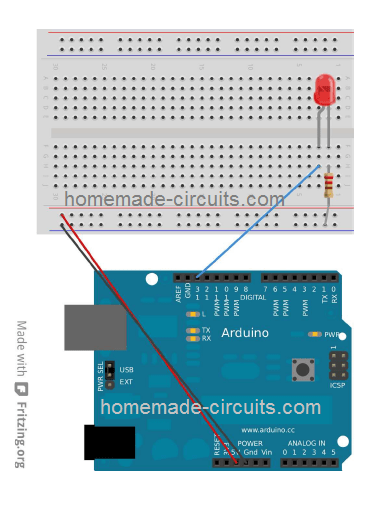 You can see 3 basic components above:
A 5mm, 20mA LED
a 330 ohm 1/4 watt resistor
An Arduino Board
Just assemble the system as per the diagram.
Next, plug in the 5V from computer USB to the Arduino.
As soon as you do this you will see the LED lighting up.
I know that's pretty basic, but it's always good to start from the scratch.
Rest assured things will start getting more and more interesting as we move ahead.
You can see 3 basic components above:
A 5mm, 20mA LED
a 330 ohm 1/4 watt resistor
An Arduino Board
Just assemble the system as per the diagram.
Next, plug in the 5V from computer USB to the Arduino.
As soon as you do this you will see the LED lighting up.
I know that's pretty basic, but it's always good to start from the scratch.
Rest assured things will start getting more and more interesting as we move ahead.
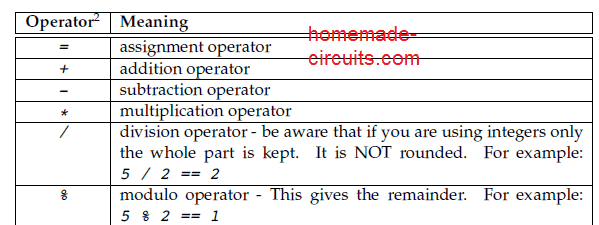 Now let's assess the codes between line 13 an 15.
 In our above code, we could have tested the code to be
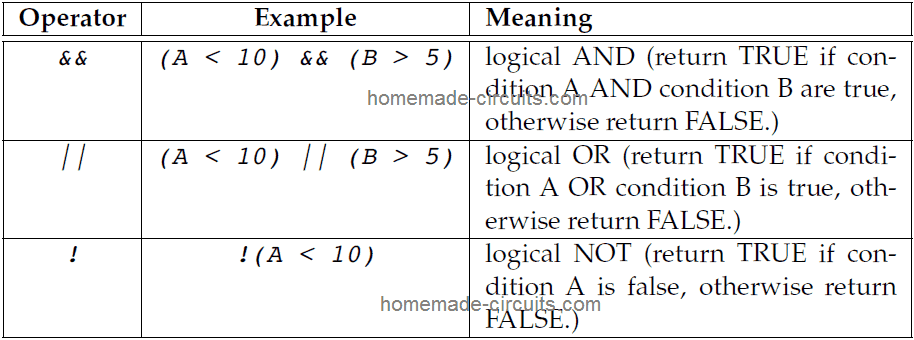 It would be interesting to know that the NOT operator can work as a switcher for a variable which may be designated to be either true or false (or LOW or HIGH).
The following example illustrates the condition:
It would be interesting to know that the NOT operator can work as a switcher for a variable which may be designated to be either true or false (or LOW or HIGH).
The following example illustrates the condition:
 You will find that there are 3 sub-statements in a for statement.
It is structured as shown below:
You will find that there are 3 sub-statements in a for statement.
It is structured as shown below:
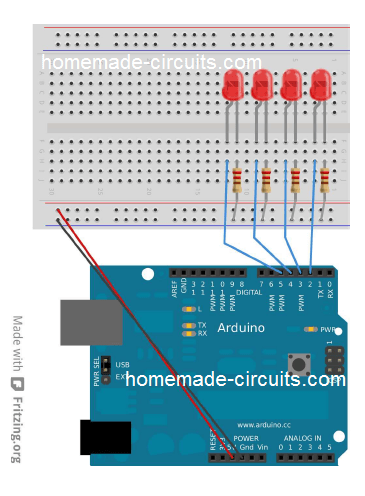 Now let's fix a program which will enable us to check whether our hardware is correctly configured or not.
It is always recommended to code and execute small bits of programs step wise to check if the respective hardwares are wired correctly or not.
This helps troubleshooting a possible error quickly.
The code example below provides LED 2 to 5 a specific pattern by turning them one after the other in a cyclic manner.
Now let's fix a program which will enable us to check whether our hardware is correctly configured or not.
It is always recommended to code and execute small bits of programs step wise to check if the respective hardwares are wired correctly or not.
This helps troubleshooting a possible error quickly.
The code example below provides LED 2 to 5 a specific pattern by turning them one after the other in a cyclic manner.
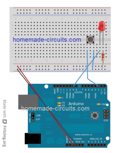 We'll connect the Arduino with a push-button with Arduino as per the above shown details and learn the basic working and implementation of the set up.
The indicated push button which is also called a micro switch push button, have 4 pins in total (2 pairs on each side).
When pushed, each pair of pins are joined internally and a enable a connection or conduction across them.
In this example we are using just one pair of these pins or contacts, the other pair is irrelevant and therefore is ignored.
Let's proceed are applying the following code and check out it working!
We'll connect the Arduino with a push-button with Arduino as per the above shown details and learn the basic working and implementation of the set up.
The indicated push button which is also called a micro switch push button, have 4 pins in total (2 pairs on each side).
When pushed, each pair of pins are joined internally and a enable a connection or conduction across them.
In this example we are using just one pair of these pins or contacts, the other pair is irrelevant and therefore is ignored.
Let's proceed are applying the following code and check out it working!
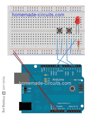 Setup the Arduino and other parameters as shown above.
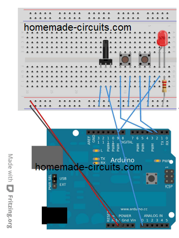 Connect the shown parameters with your Arduino as shown above.
A pot will have 3 terminals.
The middle terminasl will connect withANALOG IN 0 on the Arduino.
The other two outer terminals may be connected to +5V and 0V supply rails.
Let's program and check out the results:
Connect the shown parameters with your Arduino as shown above.
A pot will have 3 terminals.
The middle terminasl will connect withANALOG IN 0 on the Arduino.
The other two outer terminals may be connected to +5V and 0V supply rails.
Let's program and check out the results:
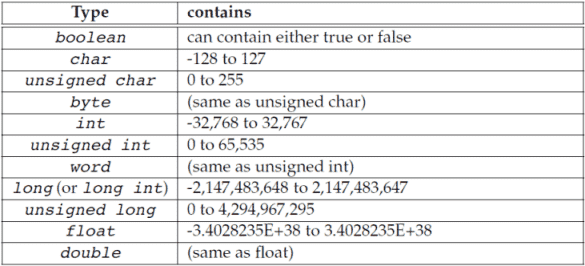 Presently, it may be only crucial to know that for storing relatively large numbers for the int variable, you could use the term long or along int.
Here you can see another interesting function calledmillis().
This produces the time span in milliseconds the Arduino worked in its course of operation from the beginning (this will reset to 0 after every 50 days).
Here it returns a long because if it returned int, counting for long periods may not be possible.
Could you answer exactly how long? Answer is32.767 seconds.
Therefore instead of usingdelay(), we check formillis(), and as soon as the particular number of milliseconds lapses we change the LED.
Consequently we store the time we changed it last in lastTime variable, so that it allows us to check it again whenever desired.
Presently, it may be only crucial to know that for storing relatively large numbers for the int variable, you could use the term long or along int.
Here you can see another interesting function calledmillis().
This produces the time span in milliseconds the Arduino worked in its course of operation from the beginning (this will reset to 0 after every 50 days).
Here it returns a long because if it returned int, counting for long periods may not be possible.
Could you answer exactly how long? Answer is32.767 seconds.
Therefore instead of usingdelay(), we check formillis(), and as soon as the particular number of milliseconds lapses we change the LED.
Consequently we store the time we changed it last in lastTime variable, so that it allows us to check it again whenever desired.
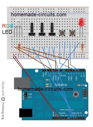 It may look a little complex, but actually it's a replica of our earlier LED control design using PWM.
Here's a practice program code:
It may look a little complex, but actually it's a replica of our earlier LED control design using PWM.
Here's a practice program code:
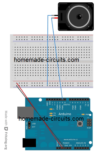
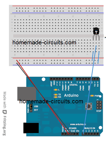 The following code will initiate the measurement of temperature by reading the output from the TMP36 sensor, and by sending them to the serial monitor of the ID.
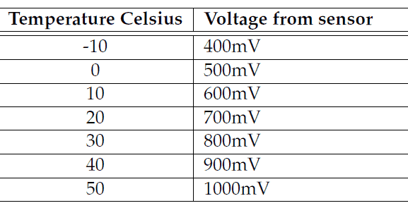 You can consider to be your first function which returns some value (note that all the remaining functions so far didn't return any value since they've been of the type void).
You can understand that in order to get a value from a function, you simply need to add return followed by the desired number you want to return.
When we say return it means the function returns a response or a reply whenever it is called, which could be applied to a variable.
When this is send to the Serial Monitor, the reading gets converted toFahrenheit throughconvertToF().
You can consider to be your first function which returns some value (note that all the remaining functions so far didn't return any value since they've been of the type void).
You can understand that in order to get a value from a function, you simply need to add return followed by the desired number you want to return.
When we say return it means the function returns a response or a reply whenever it is called, which could be applied to a variable.
When this is send to the Serial Monitor, the reading gets converted toFahrenheit throughconvertToF().
 Now let's see how we can connect the LCD and the relevant parameters with our Arduino.
The details can be visualized in the below shown illustration:
Now let's see how we can connect the LCD and the relevant parameters with our Arduino.
The details can be visualized in the below shown illustration:
 As we all know, LDR is a light dependent resistor device whose resistance depends on the intensity of the ambient incident on its surface.
The intensity of light is inversely proportional to the resistance reading of the LDR.
Here we will learn how this property can be integrated with Arduino for executing an useful application:
The complete program code can be visualized as given below:
As we all know, LDR is a light dependent resistor device whose resistance depends on the intensity of the ambient incident on its surface.
The intensity of light is inversely proportional to the resistance reading of the LDR.
Here we will learn how this property can be integrated with Arduino for executing an useful application:
The complete program code can be visualized as given below:
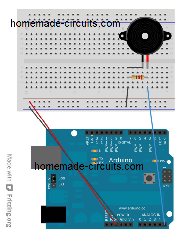
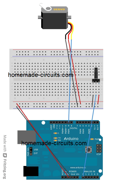 The code is given below:
 Interfacing DHTxx Temperature Humidity Sensor with Arduino
 In this tutorial we're going to have a look at DHTxx series sensors, which is often used for measuring temperatures and humidity, both features are built-into a single module.
Smart Automatic ON/OFF Switch Using Arduino
In this tutorial we're going to have a look at DHTxx series sensors, which is often used for measuring temperatures and humidity, both features are built-into a single module.
Smart Automatic ON/OFF Switch Using Arduino
 In this post we intend to develop an intelligent automatic ON/OFF switch using Arduino, which could switch on or off devices auto-magically by detecting the existence of human being locally using ultrasonic strategy.
Ultrasonic Distance Meter Circuit Using Arduino and 16¡Á2 LCD
In this post we intend to develop an intelligent automatic ON/OFF switch using Arduino, which could switch on or off devices auto-magically by detecting the existence of human being locally using ultrasonic strategy.
Ultrasonic Distance Meter Circuit Using Arduino and 16¡Á2 LCD
 In this posting we will develop an ultrasonic distance meter circuit using Arduino and 16¡Á2 LCD.
We are additionally find exactly what an ultrasonic module is, how it functions and just how it could be accustomed to calculate distance.
Home Security Circuit Using Arduino
In this posting we will develop an ultrasonic distance meter circuit using Arduino and 16¡Á2 LCD.
We are additionally find exactly what an ultrasonic module is, how it functions and just how it could be accustomed to calculate distance.
Home Security Circuit Using Arduino
 Within this article we're going to find out how to develop a home security system circuit applying arduino which could safeguard your house from burglars some day.
Housebreaking takes place just about every few seconds worldwide.
Digital Clock Circuit Using Arduino and 16¡Á2 LCD Display
Within this article we're going to find out how to develop a home security system circuit applying arduino which could safeguard your house from burglars some day.
Housebreaking takes place just about every few seconds worldwide.
Digital Clock Circuit Using Arduino and 16¡Á2 LCD Display
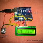 Here we learn how to make a simple digital clock using Arduino and a 16 x 2 LCD display, which can be built by any new engineering student for displaying to his colleagues or even for portraying science exhibitions
Make Arduino on Breadboard
Here we learn how to make a simple digital clock using Arduino and a 16 x 2 LCD display, which can be built by any new engineering student for displaying to his colleagues or even for portraying science exhibitions
Make Arduino on Breadboard
 On this page we will figure out how to create an arduino on a breadboard.
We are also going to discover exactly what is an arduino, the way to program this and the best way to assemble them as standalone microcontroller over a breadboard or PCB.
Foolproof IR Remote Control Circuit Using Arduino
On this page we will figure out how to create an arduino on a breadboard.
We are also going to discover exactly what is an arduino, the way to program this and the best way to assemble them as standalone microcontroller over a breadboard or PCB.
Foolproof IR Remote Control Circuit Using Arduino
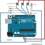 In this article we intend to build an easy to customize IR (infrared) based wireless remote control switch, which includes IR remote and also a receiver, you could possibly improve based on your preferences.
During the later portion of the article we understand an enhanced foolproof version of an IR remote control
Arduino Digital Clock Using RTC Module
In this article we intend to build an easy to customize IR (infrared) based wireless remote control switch, which includes IR remote and also a receiver, you could possibly improve based on your preferences.
During the later portion of the article we understand an enhanced foolproof version of an IR remote control
Arduino Digital Clock Using RTC Module
 This post explains how to construct a digital clock using RTC or Real Time Clock module.
We will make an to understand what an ¡°RTC¡± module is designed for, and how one could interface the module with Arduino and its functioning.
7 Segment Digital Clock Circuit Using Arduino
This post explains how to construct a digital clock using RTC or Real Time Clock module.
We will make an to understand what an ¡°RTC¡± module is designed for, and how one could interface the module with Arduino and its functioning.
7 Segment Digital Clock Circuit Using Arduino
 In this post we are going to construct a digital clock using 7 segment LED display with Arduino controlled design.
The proposed 7 segment clock circuit is inexpensive and even beginner in Arduino can accomplish it with ease.
This clock consists of four 7 segment displays, two for [¡]
LED Room Thermometer Circuit using Arduino
In this post we are going to construct a digital clock using 7 segment LED display with Arduino controlled design.
The proposed 7 segment clock circuit is inexpensive and even beginner in Arduino can accomplish it with ease.
This clock consists of four 7 segment displays, two for [¡]
LED Room Thermometer Circuit using Arduino
 In this article, we will try to understand an Arduino based LED room thermometer circuit for displaying the temperature measurement through doted/bar LEDs.
This project could be used for applications where ambient temperature is supposed to cause a crucial effect over a target or simply this could just one of your another fun project.
Automatic Temperature Regulator Circuit using Arduino
In this article, we will try to understand an Arduino based LED room thermometer circuit for displaying the temperature measurement through doted/bar LEDs.
This project could be used for applications where ambient temperature is supposed to cause a crucial effect over a target or simply this could just one of your another fun project.
Automatic Temperature Regulator Circuit using Arduino
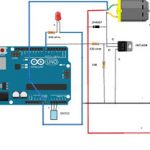 The following article will help you to construct a simple automatic temperature regulator circuit which can be used for switching on your ceiling fan or any other preferred electrical gadgets connected to it, when the ambient temperature reaches or crosses a preset threshold level.
Digital Temperature, Humidity Meter Using Arduino
The following article will help you to construct a simple automatic temperature regulator circuit which can be used for switching on your ceiling fan or any other preferred electrical gadgets connected to it, when the ambient temperature reaches or crosses a preset threshold level.
Digital Temperature, Humidity Meter Using Arduino
 In one of our earlier articles, we learned a simple method to interface temperature humidity sensor with arduino and read out displayed on serial monitor of arduino IDE.
Here let's understand how to display the reading on a 16¡Á2 LCD display for the proposed digital temperature/humidity meter.
GSM Fire SMS Alert Circuit using Arduino
In one of our earlier articles, we learned a simple method to interface temperature humidity sensor with arduino and read out displayed on serial monitor of arduino IDE.
Here let's understand how to display the reading on a 16¡Á2 LCD display for the proposed digital temperature/humidity meter.
GSM Fire SMS Alert Circuit using Arduino
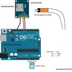 Within this post we will try to construct a GSM fire alert circuit system using Arduino and DHT11 sensor, which will alert the owner by sending text message (SMS), regarding a fire hazard within the premise where it is installed.
How to Send SMS Using GSM Modem and Arduino
Within this post we will try to construct a GSM fire alert circuit system using Arduino and DHT11 sensor, which will alert the owner by sending text message (SMS), regarding a fire hazard within the premise where it is installed.
How to Send SMS Using GSM Modem and Arduino
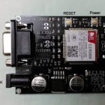 In this article students can learn, how we can send SMS using GSM modem controlled with an Arduino circuit.
We will try to learn see about GSM modem, how it may be interfaced with Arduino, how to send SMS using this setup.
How to Receive SMS Using GSM Modem and Arduino
In this article students can learn, how we can send SMS using GSM modem controlled with an Arduino circuit.
We will try to learn see about GSM modem, how it may be interfaced with Arduino, how to send SMS using this setup.
How to Receive SMS Using GSM Modem and Arduino
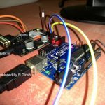 In this post we will elaborately learn how to receive SMS using GSM modem, and Arduino.
In one the previous post we understood how to send a text message using GSM modem and also discussed the basics the GSM modem.
Password Security Lock Circuit Using Arduino and 4¡Á4 Keypad
In this post we will elaborately learn how to receive SMS using GSM modem, and Arduino.
In one the previous post we understood how to send a text message using GSM modem and also discussed the basics the GSM modem.
Password Security Lock Circuit Using Arduino and 4¡Á4 Keypad
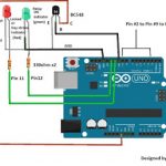 In this special engineering project we will try to construct a password security lock circuit, which will be accept and open by a 6-digit password.
Precisely speaking it is alpha numeric password and will require a 4¡Á4 keypad, consisting of 0 to 9 decimal values, two special character
How to Interface 4¡Á4 Keypad with Arduino
In this special engineering project we will try to construct a password security lock circuit, which will be accept and open by a 6-digit password.
Precisely speaking it is alpha numeric password and will require a 4¡Á4 keypad, consisting of 0 to 9 decimal values, two special character
How to Interface 4¡Á4 Keypad with Arduino
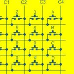 In this article we will investigate how to interface a 4¡Á4 keypad with Arduino.
We will learn what is a keypad, how it may be built and a learn to program the Arduino for accepting keystrokes through the keypad and print them in serial monitor.
Simple Calculator Circuit Using Arduino
In this article we will investigate how to interface a 4¡Á4 keypad with Arduino.
We will learn what is a keypad, how it may be built and a learn to program the Arduino for accepting keystrokes through the keypad and print them in serial monitor.
Simple Calculator Circuit Using Arduino
 In this tutorial, we're going to develop a calculator employing Arduino, which could carry out significantly intricate arithmetical calculation compared to an ordinary calculator.
The sentenza of this write-up is not really to produce a calculator using Arduino, rather to highlight the arithmetical convenience of Arduino, that executes a variety of complex data interpretations and calculations
Make this RFID Circuit using Arduino
In this tutorial, we're going to develop a calculator employing Arduino, which could carry out significantly intricate arithmetical calculation compared to an ordinary calculator.
The sentenza of this write-up is not really to produce a calculator using Arduino, rather to highlight the arithmetical convenience of Arduino, that executes a variety of complex data interpretations and calculations
Make this RFID Circuit using Arduino
 In this another great engineering project we're going to have a look at RFID circuit technology.
We will be investigating just how RFID tags and readers operate, the way to interface RFID module (RC522) together with Arduino and draw out many helpful data from the RFID tags.
Barometric Pressure Sensor Circuit using Arduino
In this another great engineering project we're going to have a look at RFID circuit technology.
We will be investigating just how RFID tags and readers operate, the way to interface RFID module (RC522) together with Arduino and draw out many helpful data from the RFID tags.
Barometric Pressure Sensor Circuit using Arduino
 In the following sections we intend to examine, what is a Barometer and how to integrate a barometric BMP180 sensor with Arduino.
We shall likewise investigate a few of its crucial specification and lastly we will figure out how to anticipate weather conditions employing barometric readings.
How to Make LED Air Pollution Meter Circuit
In the following sections we intend to examine, what is a Barometer and how to integrate a barometric BMP180 sensor with Arduino.
We shall likewise investigate a few of its crucial specification and lastly we will figure out how to anticipate weather conditions employing barometric readings.
How to Make LED Air Pollution Meter Circuit
 In this particular assignment we intend to build an air pollution meter applying MQ-135 sensor and arduino.
The pollution grade in the surroundings will be displayed by group of 12 LED.
The number of LED glowing gives proportionately higher degree of pollution level and vice versa
LPG Leakage SMS Alert Circuit using Arduino and MQ-135
In this particular assignment we intend to build an air pollution meter applying MQ-135 sensor and arduino.
The pollution grade in the surroundings will be displayed by group of 12 LED.
The number of LED glowing gives proportionately higher degree of pollution level and vice versa
LPG Leakage SMS Alert Circuit using Arduino and MQ-135
 This post is for all those engineers who intend to develop a GSM based LPG leakage SMS alert circuit working with Arduino.
This unit will forewarn the beneficiary through SMS and encircling folks through buzzer beep, whenever LPG gas tends to leak out from an LPG cylinder or leaks as a result of badly shut valve.
How to Make a DC Voltmeter using Arduino
This post is for all those engineers who intend to develop a GSM based LPG leakage SMS alert circuit working with Arduino.
This unit will forewarn the beneficiary through SMS and encircling folks through buzzer beep, whenever LPG gas tends to leak out from an LPG cylinder or leaks as a result of badly shut valve.
How to Make a DC Voltmeter using Arduino
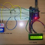 On this page, we're going to build a DC voltmeter using Arduino in which the readings are viewed in 16¡Á2 LCD.
The recommended voltmeter layout is designed to read through as much as 30V with tolerance of +/- 0.5 volt.
We intend to observe how this particular setup performs and check out additional options
MQ-135 Air Quality Sensor with Arduino
On this page, we're going to build a DC voltmeter using Arduino in which the readings are viewed in 16¡Á2 LCD.
The recommended voltmeter layout is designed to read through as much as 30V with tolerance of +/- 0.5 volt.
We intend to observe how this particular setup performs and check out additional options
MQ-135 Air Quality Sensor with Arduino
 Here we will discover how to attach an air quality sensor MQ-135 with Arduino.
We will learn the summary of the sensor and develop a nice little project specially dedicated to engineers that will detecting LPG gas leakage and find out several pertinent readings in serial monitor.
GSM Pump Motor Controller Circuit using Arduino
Here we will discover how to attach an air quality sensor MQ-135 with Arduino.
We will learn the summary of the sensor and develop a nice little project specially dedicated to engineers that will detecting LPG gas leakage and find out several pertinent readings in serial monitor.
GSM Pump Motor Controller Circuit using Arduino
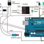 In this article we develop a helpful GSM pump motor controller circuit for the farmers which can switch on and off the irrigation water system distantly from around the globe through cellphone SMS and revert you with an acknowledgement message in your cellphone.
SMS Based Laser Security Circuit using Arduino
In this article we develop a helpful GSM pump motor controller circuit for the farmers which can switch on and off the irrigation water system distantly from around the globe through cellphone SMS and revert you with an acknowledgement message in your cellphone.
SMS Based Laser Security Circuit using Arduino
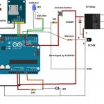 Through this post, we are going to discuss methods to construct a laser security circuit that will send out SMS alert to the holder of the property or the concerned consumer and switch on obnoxious alarm to discourage the criminal, which is often interfaced via relay.
Simple Arduino Digital Ohmmeter Circuit
Through this post, we are going to discuss methods to construct a laser security circuit that will send out SMS alert to the holder of the property or the concerned consumer and switch on obnoxious alarm to discourage the criminal, which is often interfaced via relay.
Simple Arduino Digital Ohmmeter Circuit
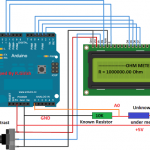 This specific post tells us regarding the construction of a simple digital ohmmeter circuit using Arduino and 16¡Á2 LCD display.
We are going to additionally be studying the various other achievable circuit ideas using the very same theory.
Battery Level Indicator Circuit using Arduino
This specific post tells us regarding the construction of a simple digital ohmmeter circuit using Arduino and 16¡Á2 LCD display.
We are going to additionally be studying the various other achievable circuit ideas using the very same theory.
Battery Level Indicator Circuit using Arduino
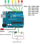 Inside this post, we will discuss how to set up a battery level indicator using Arduino, in which a group of 6 LEDs demonstrate level of the battery.
In case you are considering keeping track of repairs and maintenance of your 12V battery, this circuit may possibly turn out to be useful.
Battery Over Discharge Protection Circuit Using Arduino
Inside this post, we will discuss how to set up a battery level indicator using Arduino, in which a group of 6 LEDs demonstrate level of the battery.
In case you are considering keeping track of repairs and maintenance of your 12V battery, this circuit may possibly turn out to be useful.
Battery Over Discharge Protection Circuit Using Arduino
 If you are an electrical engineer then you will like this tutorial.
Here we're going to create an over discharge protection circuit for 12v battery using Arduino which could safeguard 12V SLA battery against over discharge, as well as safeguard the attached load from rising voltage if an overcharged battery is accidentally hooked up.
RFID Security Lock Circuit using Arduino
If you are an electrical engineer then you will like this tutorial.
Here we're going to create an over discharge protection circuit for 12v battery using Arduino which could safeguard 12V SLA battery against over discharge, as well as safeguard the attached load from rising voltage if an overcharged battery is accidentally hooked up.
RFID Security Lock Circuit using Arduino
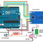 In the following paragraphs we will find out how an Arduino based RFID reader circuit could possibly be intended for controlling a relay, that in turn may be utilized for controlling security door lock applications.
Automatic Street Light Dimmer using Arduino
In the following paragraphs we will find out how an Arduino based RFID reader circuit could possibly be intended for controlling a relay, that in turn may be utilized for controlling security door lock applications.
Automatic Street Light Dimmer using Arduino
 On this page we intend to construct an Arduino automatic street light dimmer circuit, that may cut down its brightness or intensity of the lamp when no automobile may be passing within the road in order to save power.
LED Strip Light Controller Using Arduino
On this page we intend to construct an Arduino automatic street light dimmer circuit, that may cut down its brightness or intensity of the lamp when no automobile may be passing within the road in order to save power.
LED Strip Light Controller Using Arduino
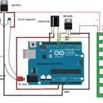 From this post you are going to learn how to construct LED strip controller circuit applying Arduino, that may turn ON/OFF and decrease/increase illumination levels of LEDs using ordinary IR (Infrared) remote.
Do you know what is LED Strip Light? If you are not knowledgeable about LED strip lights, we will elaborately understand what it is
How to Interface Servo motors with Arduino
From this post you are going to learn how to construct LED strip controller circuit applying Arduino, that may turn ON/OFF and decrease/increase illumination levels of LEDs using ordinary IR (Infrared) remote.
Do you know what is LED Strip Light? If you are not knowledgeable about LED strip lights, we will elaborately understand what it is
How to Interface Servo motors with Arduino
 Here engineering students can learn exactly what servo motor is, exactly how it works, how you can interface with microcontroller and exactly what make this motor unique compared to other motors.
Simple Arduino Modified Sine Wave Inverter Circuit
Here engineering students can learn exactly what servo motor is, exactly how it works, how you can interface with microcontroller and exactly what make this motor unique compared to other motors.
Simple Arduino Modified Sine Wave Inverter Circuit
 Inside this post we intend to develop a modified sine wave inverter using Arduino.
We are going to check out the strategy of the suggested sine wave inverter and eventually, we are going to have a look at lab-created output of this inverter.
How to Interface Accelerometer ADXL335 with Arduino
Inside this post we intend to develop a modified sine wave inverter using Arduino.
We are going to check out the strategy of the suggested sine wave inverter and eventually, we are going to have a look at lab-created output of this inverter.
How to Interface Accelerometer ADXL335 with Arduino
 Throughout this article, we plan to find how to use an accelerometer with arduino and acquire valuable readings, that will probably be printed on serial monitor of IDE.
We will furthermore be discovering briefly how accelerometer performs and its applications ranges.
IC 555 Inverter with Arduino Hi/Low Battery Shutdown Circuit
Throughout this article, we plan to find how to use an accelerometer with arduino and acquire valuable readings, that will probably be printed on serial monitor of IDE.
We will furthermore be discovering briefly how accelerometer performs and its applications ranges.
IC 555 Inverter with Arduino Hi/Low Battery Shutdown Circuit
 In this inverter design we make use of a 4017 decade counter and a ne555 timer Ic to crank out a sinewave pwm signal for the inverter and an Arduino based automatic high/low battery cut-off with alarm.
Frequency Meter Circuit Using Arduino and 16¡Á2 Display
In this inverter design we make use of a 4017 decade counter and a ne555 timer Ic to crank out a sinewave pwm signal for the inverter and an Arduino based automatic high/low battery cut-off with alarm.
Frequency Meter Circuit Using Arduino and 16¡Á2 Display
 Within this informative article we intend to build a digital frequency meter using Arduino whose readings is going to be exhibited on a 16¡Á2 LCD display and will possess a computing range from 35 Hz to 1MHz.
Arduino Pure Sine Wave Inverter Circuit
Within this informative article we intend to build a digital frequency meter using Arduino whose readings is going to be exhibited on a 16¡Á2 LCD display and will possess a computing range from 35 Hz to 1MHz.
Arduino Pure Sine Wave Inverter Circuit
 This article describes a simple pure sine wave inverter circuit using Arduino, which may be enhanced to accomplish any desired power output in accordance with the user¡¯s inclination
Arduino SPWM Generator Circuit
This article describes a simple pure sine wave inverter circuit using Arduino, which may be enhanced to accomplish any desired power output in accordance with the user¡¯s inclination
Arduino SPWM Generator Circuit
 In this post we figure out how to crank out sine wave pulse-width-modulation or SPWM through Arduino, which may be utilized for setting up a pure sine wave inverter circuit or comparable gadgets.
How to Interface Cellphone Display with Arduino
In this post we figure out how to crank out sine wave pulse-width-modulation or SPWM through Arduino, which may be utilized for setting up a pure sine wave inverter circuit or comparable gadgets.
How to Interface Cellphone Display with Arduino
 Through this Arduino we will be finding out how to interface Nokia 5110 display with Arduino microcontroller and how to exhibit a few text, we are going to additionally learn to develop a simple digital clock and ultimately we will be checking out graphical features of the Nokia 5110 display.
Automatic Stopwatch Circuit for Runners
Through this Arduino we will be finding out how to interface Nokia 5110 display with Arduino microcontroller and how to exhibit a few text, we are going to additionally learn to develop a simple digital clock and ultimately we will be checking out graphical features of the Nokia 5110 display.
Automatic Stopwatch Circuit for Runners
 Through this article we're going to build a stopwatch which automatically starts a timer once the runner has started of running and the timer stop as soon as the runner touches the finish point.
The elapsed time between starting and ending point becomes viewable on a 16 x 2 LCD.
Mini Weather Station Using Arduino
Through this article we're going to build a stopwatch which automatically starts a timer once the runner has started of running and the timer stop as soon as the runner touches the finish point.
The elapsed time between starting and ending point becomes viewable on a 16 x 2 LCD.
Mini Weather Station Using Arduino
 In this post final year engineering students can develop an appealing Arduino based mini weather station project, which could demonstrate ambient temperature, humidity, pressure, air quality plus much more info from your environment, and could be implemented to anticipate weather in homes.
This concludes our list of 50 best Arduino projects for final year engineering students.
More such interesting circuit projects will be updated as more articles are published in this website.
If you have any related questions, please feel free to ask them through the below given comment box.
In this post final year engineering students can develop an appealing Arduino based mini weather station project, which could demonstrate ambient temperature, humidity, pressure, air quality plus much more info from your environment, and could be implemented to anticipate weather in homes.
This concludes our list of 50 best Arduino projects for final year engineering students.
More such interesting circuit projects will be updated as more articles are published in this website.
If you have any related questions, please feel free to ask them through the below given comment box.
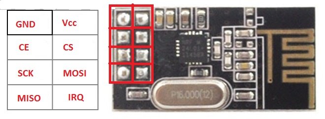 The above chip is called nRF24L01 module.
It is a duplex (bi-directional) communication circuit board designed for microcontrollers and single board computers like Raspberry Pi.
It utilizes 2.4 GHz frequency which is ISM band (Industrial, Scientific and Medical band) it is the same frequency used in Wi-Fi communication.
It can transmit or receive data at the rate of 2Mbps, but in this project the transmission and reception is limited to 250 Kbps because of lower data requirements and lowering the data rate will results in increased overall range.
It consumes only 12.3 mA at peak data transmission which makes battery friendly device.
It utilizes SPI protocol for communicating with microcontroller.
It has transmission / reception range of 100 meter with no obstacle in between and about 30 meter range with some obstacle.
You can find this module on popular e-commerce sites, also at your local electronics store.
Note: The module can work from 1.9 to 3.6V, the on board regulator on the Arduino can provide 3.3V for the module.
If you connect the nRF24L01¡¯s Vcc terminal to 5V of Arduino¡¯s output, this will result in malfunction of the module.
So care must be taken.
That¡¯s the brief introduction to the nRF24L01 module.
Let¡¯s investigate the details of the circuit diagram:
The above chip is called nRF24L01 module.
It is a duplex (bi-directional) communication circuit board designed for microcontrollers and single board computers like Raspberry Pi.
It utilizes 2.4 GHz frequency which is ISM band (Industrial, Scientific and Medical band) it is the same frequency used in Wi-Fi communication.
It can transmit or receive data at the rate of 2Mbps, but in this project the transmission and reception is limited to 250 Kbps because of lower data requirements and lowering the data rate will results in increased overall range.
It consumes only 12.3 mA at peak data transmission which makes battery friendly device.
It utilizes SPI protocol for communicating with microcontroller.
It has transmission / reception range of 100 meter with no obstacle in between and about 30 meter range with some obstacle.
You can find this module on popular e-commerce sites, also at your local electronics store.
Note: The module can work from 1.9 to 3.6V, the on board regulator on the Arduino can provide 3.3V for the module.
If you connect the nRF24L01¡¯s Vcc terminal to 5V of Arduino¡¯s output, this will result in malfunction of the module.
So care must be taken.
That¡¯s the brief introduction to the nRF24L01 module.
Let¡¯s investigate the details of the circuit diagram:
 The remote consists of Arduino nano; by the way you can use any Arduino board, 6 push buttons for ringing six different receivers, nRF24L01 module and a LED for acknowledging the push of a button.
You can power this using 9V battery or from 5V adapter.
In case of battery you should turn off this remote after your call.
Now let¡¯s look at the code.
Before that you need to download the library file only then the code gets compiled.
Link: github.com/nRF24/RF24.git
The remote consists of Arduino nano; by the way you can use any Arduino board, 6 push buttons for ringing six different receivers, nRF24L01 module and a LED for acknowledging the push of a button.
You can power this using 9V battery or from 5V adapter.
In case of battery you should turn off this remote after your call.
Now let¡¯s look at the code.
Before that you need to download the library file only then the code gets compiled.
Link: github.com/nRF24/RF24.git
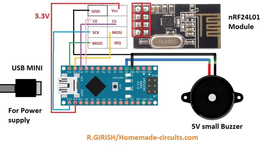 Now let¡¯s look at the code for receiver:
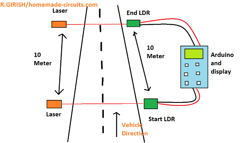 We know the distance is 10 meter which is fixed, now we have to know the time in the equation.
The time will be calculated by Arduino, when the vehicle interrupts the ¡°start laser¡±, the timer begins and when the vehicle interrupts the ¡°end laser¡± the timer stops and applying the values to the equation Arduino will find the speed of the vehicle.
Please note that speed of the vehicle will only be detected in one direction i.e.
start laser to stop laser, to detect the vehicle in another direction another same setup has to be place on opposite direction.
So, this is ideal for places like school, collage etc.
where they have IN and OUT gates.
Now let¡¯s see the schematic diagram:
We know the distance is 10 meter which is fixed, now we have to know the time in the equation.
The time will be calculated by Arduino, when the vehicle interrupts the ¡°start laser¡±, the timer begins and when the vehicle interrupts the ¡°end laser¡± the timer stops and applying the values to the equation Arduino will find the speed of the vehicle.
Please note that speed of the vehicle will only be detected in one direction i.e.
start laser to stop laser, to detect the vehicle in another direction another same setup has to be place on opposite direction.
So, this is ideal for places like school, collage etc.
where they have IN and OUT gates.
Now let¡¯s see the schematic diagram:
 There above circuit is self-explanatory and just connect the wiring as per the circuit.
Adjust the 10K potentiometer for adjusting the display contrast.
There above circuit is self-explanatory and just connect the wiring as per the circuit.
Adjust the 10K potentiometer for adjusting the display contrast.
 The above circuit consists of Arduino, 4 push buttons, two 10K pull down resistors (don¡¯t change the value of resistors), two LDRs and one buzzer.
The function of 4 push buttons will be explained shortly.
Now let¡¯s see how to mount the LDR properly.
The above circuit consists of Arduino, 4 push buttons, two 10K pull down resistors (don¡¯t change the value of resistors), two LDRs and one buzzer.
The function of 4 push buttons will be explained shortly.
Now let¡¯s see how to mount the LDR properly.
 The LDR must me covered from the sunlight properly, only the laser beam should strike the LDR.
Make sure that your laser module is powerful enough to work in a bright sun shine.
You can use a PVC pipe for the above purpose and paint it black inside the tube; don¡¯t forget to cover the front part, use your creativity to accomplish this.
The LDR must me covered from the sunlight properly, only the laser beam should strike the LDR.
Make sure that your laser module is powerful enough to work in a bright sun shine.
You can use a PVC pipe for the above purpose and paint it black inside the tube; don¡¯t forget to cover the front part, use your creativity to accomplish this.
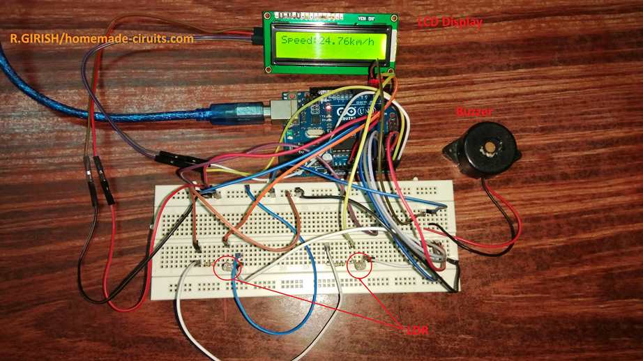 If have any questions regarding this traffic police vehicle speed detector circuit, please feel free to ask in comment section, you may get a quick reply.
 The Strain gauge is flexible; it is a thin metallic foil pattern sandwiched between two thin plastic sheets and it has to be attached on a surface using suitable glue or any adhesive material.
When we apply weight or force on the surface it deforms and the strain gauge deforms as well.
The deformation of the strain gauge causes the electrical resistance of the metallic foil to change.
Now the strain gauge¡¯s change in the resistance is directly proportional to weight or applied force on the surface.
In real life the change in resistance of strain gauge is very insignificant to detect.
To detect tiny changes in the resistance we are utilizing Wheatstone bridge.
Let¡¯s explore what Wheatstone bridge is in a nutshell.
The Strain gauge is flexible; it is a thin metallic foil pattern sandwiched between two thin plastic sheets and it has to be attached on a surface using suitable glue or any adhesive material.
When we apply weight or force on the surface it deforms and the strain gauge deforms as well.
The deformation of the strain gauge causes the electrical resistance of the metallic foil to change.
Now the strain gauge¡¯s change in the resistance is directly proportional to weight or applied force on the surface.
In real life the change in resistance of strain gauge is very insignificant to detect.
To detect tiny changes in the resistance we are utilizing Wheatstone bridge.
Let¡¯s explore what Wheatstone bridge is in a nutshell.
 Our modern digital multimeters can read the resistance value ranging from mega ohms, kilo ohms and ohms range.
Using Wheat stone bridge we can measure resistance in milli ohm range.
The wheat stone bridge consists of 4 resistors, out of the four, 3 are known resistance and one is unknown resistance.
The potential difference (voltage) is applied on the points ¡°A¡± and ¡°C¡± and from points ¡°B¡± and ¡°D¡± a voltmeter is connected.
If the all the resistors are equal no current will flow at the points ¡°B¡± and ¡°D¡± and voltmeter will read zero.
This is called balanced bridge.
If a resistor¡¯s resistance is different from other three resistors, there will be voltage flow between the points ¡°B¡± and ¡°D¡± and voltmeter will read some value proportional to unknown resistance.
This is called unbalanced bridge.
Here the unknown resistance is the strain gauge, when the resistance is changed, it reflects on the voltmeter.
Now, we have converted a deformation or weight or force to voltage signal.
This voltage needs to be amplified in order to get some useful readings, which will be fed to a microcontroller to get the readings in grams.
Now let¡¯s discuss how temperature affects strain gauge performance.
Our modern digital multimeters can read the resistance value ranging from mega ohms, kilo ohms and ohms range.
Using Wheat stone bridge we can measure resistance in milli ohm range.
The wheat stone bridge consists of 4 resistors, out of the four, 3 are known resistance and one is unknown resistance.
The potential difference (voltage) is applied on the points ¡°A¡± and ¡°C¡± and from points ¡°B¡± and ¡°D¡± a voltmeter is connected.
If the all the resistors are equal no current will flow at the points ¡°B¡± and ¡°D¡± and voltmeter will read zero.
This is called balanced bridge.
If a resistor¡¯s resistance is different from other three resistors, there will be voltage flow between the points ¡°B¡± and ¡°D¡± and voltmeter will read some value proportional to unknown resistance.
This is called unbalanced bridge.
Here the unknown resistance is the strain gauge, when the resistance is changed, it reflects on the voltmeter.
Now, we have converted a deformation or weight or force to voltage signal.
This voltage needs to be amplified in order to get some useful readings, which will be fed to a microcontroller to get the readings in grams.
Now let¡¯s discuss how temperature affects strain gauge performance.
 This type of load cell is rigid and used commonly in industries.
There are 4 screw mounts, one side is bolted to a stationary surface and the other end is bolted to a holder (say basket) to hold the object to be measured.
It has maximum weight specified on the datasheet or on its body, exceeding the specification might damage the load cell.
A full bridge cells consists of 4 terminals namely E+, E-, which are excitation wires through which the supply voltage is applied.
The other two wires are S+ and S-, which are signal wires, from which the voltage is measured.
Now these voltages are in millivolt range not strong enough for a microcontroller to read and process.
We need amplification and tiny changes should be visible to the microcontroller.
To do this there are dedicated module called load cell amplifiers, let¡¯s take an overview on that.
This type of load cell is rigid and used commonly in industries.
There are 4 screw mounts, one side is bolted to a stationary surface and the other end is bolted to a holder (say basket) to hold the object to be measured.
It has maximum weight specified on the datasheet or on its body, exceeding the specification might damage the load cell.
A full bridge cells consists of 4 terminals namely E+, E-, which are excitation wires through which the supply voltage is applied.
The other two wires are S+ and S-, which are signal wires, from which the voltage is measured.
Now these voltages are in millivolt range not strong enough for a microcontroller to read and process.
We need amplification and tiny changes should be visible to the microcontroller.
To do this there are dedicated module called load cell amplifiers, let¡¯s take an overview on that.
 The load cell amplifier is based on the IC HX711 which is 24-bit analog to digital converter specifically designed for weight measures.
It has different selectable gains 32, 64 and 128 and it operates on 2.6 to 5.5 V.
This breakout board helps to detect tiny variation on load cell.
This module require HX711.h library to operate with
The load cell amplifier is based on the IC HX711 which is 24-bit analog to digital converter specifically designed for weight measures.
It has different selectable gains 32, 64 and 128 and it operates on 2.6 to 5.5 V.
This breakout board helps to detect tiny variation on load cell.
This module require HX711.h library to operate with
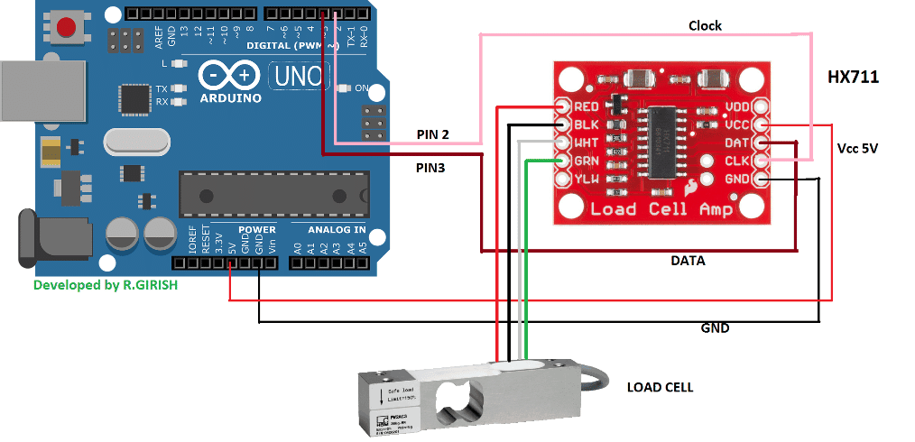 The project consists of Arduino, Load cell and HX711 load cell amplifier board and a computer.
The output can be monitored on the Serial monitor of Arduino IDE.
The brain of the project is as always the arduino, you can use any Arduino board model.
The HX711 is 24 bit ADC, which can find tiniest flex due to weight on the load cell.
It can operate from 2.7 V to 5 V.
The power is provided from Arduino board.
The load cell has four wires generally, which is the output from the Wheatstone bridge configured strain gauge.
The Red wire is E+, black wire is E-, green wire is A- and white wire is A+.
Some HX711 modules specify the name of the terminals of load cell and some HX711 modules specify the colours of the wires, such a model is illustrated in the circuit diagram.
The DATA pin of HX711 is connected to pin #3 of Arduino and Clock pin of the HX711 is connected to pin #2 of Arduino.
The project consists of Arduino, Load cell and HX711 load cell amplifier board and a computer.
The output can be monitored on the Serial monitor of Arduino IDE.
The brain of the project is as always the arduino, you can use any Arduino board model.
The HX711 is 24 bit ADC, which can find tiniest flex due to weight on the load cell.
It can operate from 2.7 V to 5 V.
The power is provided from Arduino board.
The load cell has four wires generally, which is the output from the Wheatstone bridge configured strain gauge.
The Red wire is E+, black wire is E-, green wire is A- and white wire is A+.
Some HX711 modules specify the name of the terminals of load cell and some HX711 modules specify the colours of the wires, such a model is illustrated in the circuit diagram.
The DATA pin of HX711 is connected to pin #3 of Arduino and Clock pin of the HX711 is connected to pin #2 of Arduino.
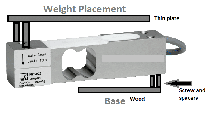 The load cell has four screw holes, two at both sides.
Any one side must be stationary for best accuracy; it may be mounded to a wood with reasonable weight.
A thin wood or thin plate can be used to hold the measuring weight as illustrated above.
So when you place a weight, the load cell bend so does the strain gauge and change its resistance which is measured by HX711 module and fed to Arduino.
Once the hardware setup is complete, let¡¯s upload the code and calibrate.
The load cell has four screw holes, two at both sides.
Any one side must be stationary for best accuracy; it may be mounded to a wood with reasonable weight.
A thin wood or thin plate can be used to hold the measuring weight as illustrated above.
So when you place a weight, the load cell bend so does the strain gauge and change its resistance which is measured by HX711 module and fed to Arduino.
Once the hardware setup is complete, let¡¯s upload the code and calibrate.
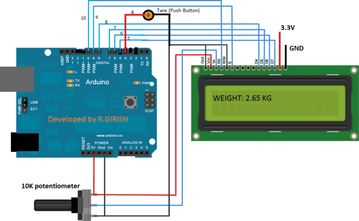 In the above schematic we have the arduino, 16 x 2 LCD display and 10K potentiometer for adjusting LCD display contrast.
3.3 V can be fed from Arduino to LCD display for backlighting.
A push button is provided to bring the weight reading to zero, this function will be explained in detail at the end.
This is just connection between LCD and Arduino, the connection between load cell and load cell amplifier to Arduino is shown in the previous section.
In the above schematic we have the arduino, 16 x 2 LCD display and 10K potentiometer for adjusting LCD display contrast.
3.3 V can be fed from Arduino to LCD display for backlighting.
A push button is provided to bring the weight reading to zero, this function will be explained in detail at the end.
This is just connection between LCD and Arduino, the connection between load cell and load cell amplifier to Arduino is shown in the previous section.
 Here we just have an Arduino and LCD display with I2C adapter on the back.
Now the wire connections are simplified and straight forward.
Here we just have an Arduino and LCD display with I2C adapter on the back.
Now the wire connections are simplified and straight forward.
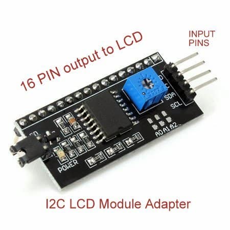 This module can be soldered directly on the back of a normal 16 x 2 or even 20 x 4 LCD display and follow the schematic diagram.
And again please refer the previous section for connection of load cell, load cell amplifier and Arduino.
Download the following Library for I2C based:
github.com/marcoschwartz/LiquidCrystal_I2C
github.com/PaulStoffregen/Wire
This module can be soldered directly on the back of a normal 16 x 2 or even 20 x 4 LCD display and follow the schematic diagram.
And again please refer the previous section for connection of load cell, load cell amplifier and Arduino.
Download the following Library for I2C based:
github.com/marcoschwartz/LiquidCrystal_I2C
github.com/PaulStoffregen/Wire
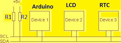 The I2C or IIC stands for ¡°Inter-Integrated Circuit¡± is a serial computer bus invented by Philips semiconductors, today known as NXP semiconductors.
This bus system was invented in 1982.
The I2C or IIC stands for ¡°Inter-Integrated Circuit¡± is a serial computer bus invented by Philips semiconductors, today known as NXP semiconductors.
This bus system was invented in 1982.

 The Adapter is soldered on the back of the LCD display and as we can see that we saved loads of GPIO pins for other tasks and also we can continue add 126 more I2C devices to pins A4 and A5.
Please note that the standard Liquid Crystal library won¡¯t work with this I2C LCD adapter, there is a special library for this, which will be covered soon and we¡¯ll show you how to use this module with coding example.
The Adapter is soldered on the back of the LCD display and as we can see that we saved loads of GPIO pins for other tasks and also we can continue add 126 more I2C devices to pins A4 and A5.
Please note that the standard Liquid Crystal library won¡¯t work with this I2C LCD adapter, there is a special library for this, which will be covered soon and we¡¯ll show you how to use this module with coding example.
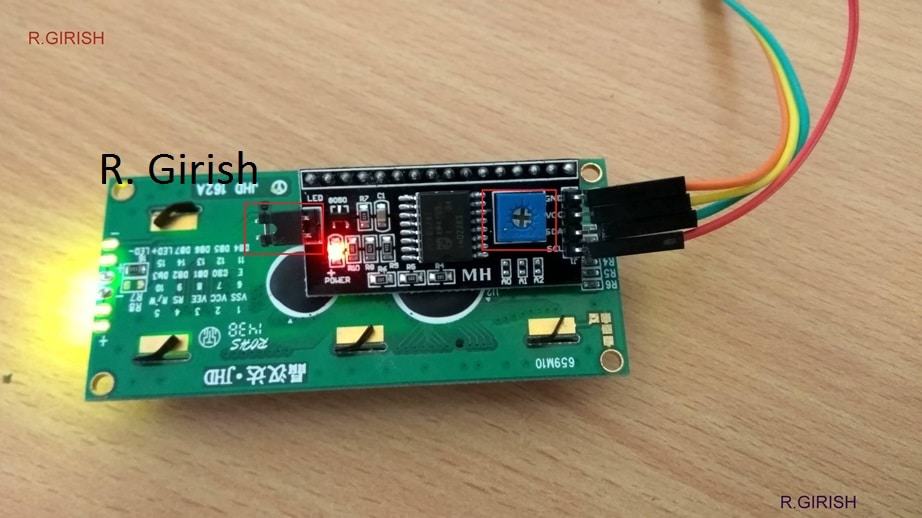 The module has 16 output pins and 4 input pins.
We can just solder the adapter to the back of the 16 x 2 LCD display.
Out of the 4 input pins, the two are +5V and GND, rest of the two are SDA and SCL.
We can see that we saved a lot of pins at Arduino for other input / output tasks.
We can adjust the contrast of the display by adjusting the potentiometer with small screw driver (highlighted in red box).
The backlighting now can be controlled in the program code itself:
lcd.backlight();
This will turn ON the backlight on the LCD display.
lcd.noBacklight();
This will turn OFF the backlight on the LCD display.
We can see there is a jumper connected, which is highlighted in red box, if the jumper is removed the backlight remains OFF regardless of the program command.
Now the hardware setup is done, now let¡¯s see how to code.
Please remember that I2C LCD module needs special
library and the pre-installed ¡°liquidcrystal¡± library won¡¯t work.
You can download the I2C LCD library from here and add to Arduino IDE:
github.com/marcoschwartz/LiquidCrystal_I2C
From the previous post we learned that I2C devices have address by which the master or the microcontroller can identify the device and communicate.
In most case, for the I2C LCD module the address would be ¡°0x27¡±.
But different manufacture may have different address.
We have to enter the correct address in the program only then your LCD display will function.
To find the address just connect 5V to Vcc and GND to GND of Arduino and SCL pin of I2C module to A5 and SDA to A4 and upload the below code.
This will scan the connected I2C devices and show their address.
The module has 16 output pins and 4 input pins.
We can just solder the adapter to the back of the 16 x 2 LCD display.
Out of the 4 input pins, the two are +5V and GND, rest of the two are SDA and SCL.
We can see that we saved a lot of pins at Arduino for other input / output tasks.
We can adjust the contrast of the display by adjusting the potentiometer with small screw driver (highlighted in red box).
The backlighting now can be controlled in the program code itself:
lcd.backlight();
This will turn ON the backlight on the LCD display.
lcd.noBacklight();
This will turn OFF the backlight on the LCD display.
We can see there is a jumper connected, which is highlighted in red box, if the jumper is removed the backlight remains OFF regardless of the program command.
Now the hardware setup is done, now let¡¯s see how to code.
Please remember that I2C LCD module needs special
library and the pre-installed ¡°liquidcrystal¡± library won¡¯t work.
You can download the I2C LCD library from here and add to Arduino IDE:
github.com/marcoschwartz/LiquidCrystal_I2C
From the previous post we learned that I2C devices have address by which the master or the microcontroller can identify the device and communicate.
In most case, for the I2C LCD module the address would be ¡°0x27¡±.
But different manufacture may have different address.
We have to enter the correct address in the program only then your LCD display will function.
To find the address just connect 5V to Vcc and GND to GND of Arduino and SCL pin of I2C module to A5 and SDA to A4 and upload the below code.
This will scan the connected I2C devices and show their address.
 As we can see two devices were detected and their addresses are displayed, but if you want to find only the address of the I2C LCD module, you should not connect any other I2C devices while scanning.
So in conclusion we got the address ¡°0x27¡±.
Now we are going to make a digital watch as example because there are two I2C devices, the LCD module and RTC or real time clock module.
The both modules will be connected with two wires.
Download the following library:
RTC library: github.com/PaulStoffregen/DS1307RTC
TimeLib.h: github.com/PaulStoffregen/Time
As we can see two devices were detected and their addresses are displayed, but if you want to find only the address of the I2C LCD module, you should not connect any other I2C devices while scanning.
So in conclusion we got the address ¡°0x27¡±.
Now we are going to make a digital watch as example because there are two I2C devices, the LCD module and RTC or real time clock module.
The both modules will be connected with two wires.
Download the following library:
RTC library: github.com/PaulStoffregen/DS1307RTC
TimeLib.h: github.com/PaulStoffregen/Time
 Program:
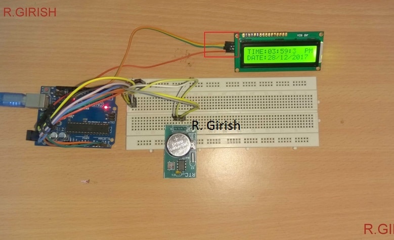 Only 4 wires are connected to the LCD display, highlighted in red box.
 Also only 4 wires are connected from Arduino and the RTC module shares the same lines.
By now you have gained basic knowledge on I2C and how to use the I2C LCD adapter module.
Do you like this post? Do you have any questions? Please express in the comment section, you may get a quick reply.
Also only 4 wires are connected from Arduino and the RTC module shares the same lines.
By now you have gained basic knowledge on I2C and how to use the I2C LCD adapter module.
Do you like this post? Do you have any questions? Please express in the comment section, you may get a quick reply.
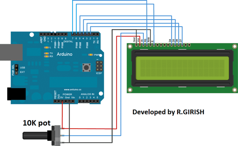
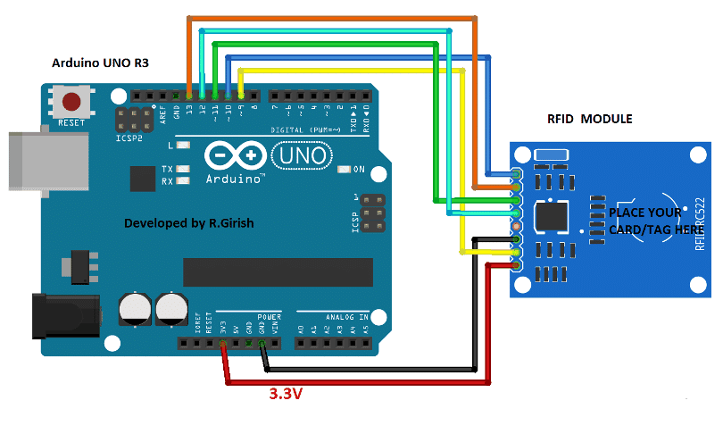 The RFID module must be powered by 3.3V and 5V can damage the on board components.
The RFID-RC522 module works on SPI communication protocol while communicating with Arduino.
The RFID module must be powered by 3.3V and 5V can damage the on board components.
The RFID-RC522 module works on SPI communication protocol while communicating with Arduino.
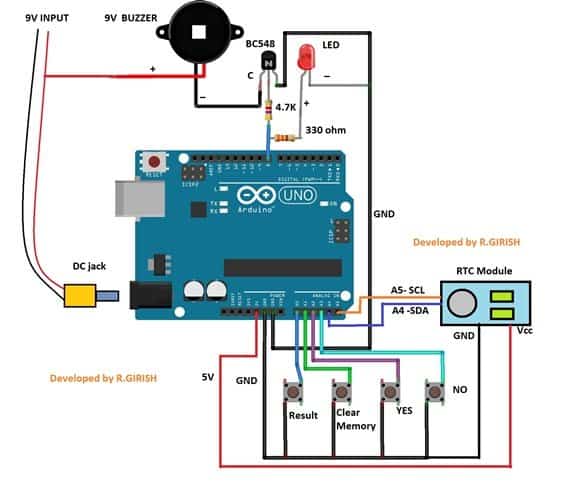 That concludes the hardware part.
Please download the following library files:
Link1: github.com/PaulStoffregen/DS1307RTC
Link2: github.com/PaulStoffregen/Time
Link3: github.com/miguelbalboa/rfid.git
Now we have to set the correct time to RTC module to do this, follow the below steps with completed hardware setup.
Open the Arduino IDE.
Navigate to File> Examples> DS1307RTC> SetTime.
Upload the code.
Once the code is uploaded to Arduino, open the serial monitor.
Now the RTC is synchronized with the time of your computer.
Now you have to find UID or unique identification number of all 12 RFID cards/tags.
To find UID, upload the below code and open the serial monitor.
That concludes the hardware part.
Please download the following library files:
Link1: github.com/PaulStoffregen/DS1307RTC
Link2: github.com/PaulStoffregen/Time
Link3: github.com/miguelbalboa/rfid.git
Now we have to set the correct time to RTC module to do this, follow the below steps with completed hardware setup.
Open the Arduino IDE.
Navigate to File> Examples> DS1307RTC> SetTime.
Upload the code.
Once the code is uploaded to Arduino, open the serial monitor.
Now the RTC is synchronized with the time of your computer.
Now you have to find UID or unique identification number of all 12 RFID cards/tags.
To find UID, upload the below code and open the serial monitor.
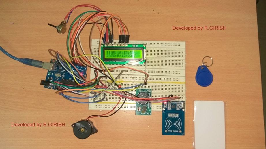 If you have any questions regarding this project, feel free to express in the comment section, you may receive a quick reply.
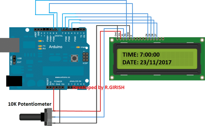
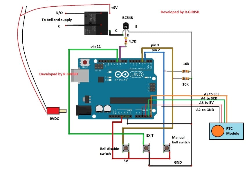 Detailed Information Regarding Bell and Relay Connections:
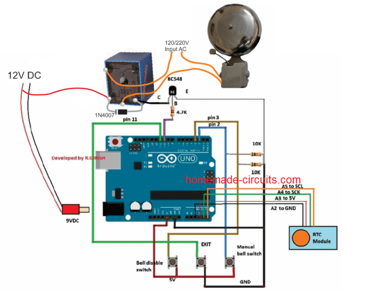 UPDATE: A5 to SCL and A4 to SDA (Not A4 to SCK)
 The connection between Arduino and GSM module as follows:
Arduino TX to RX GSM module
Arduino RX to TX GSM module
Arduino GND to GND GSM module
Never try to power the GSM module from Arduino¡¯s 5V output pin to 5V input of GSM module.
The RTC or real time clock module will track the time of arrival of water and termination of water supply.
That concludes the hardware.
To set the time on RTC we need to upload time setting program to RTC with the completed hardware setup.
This will sync the time on your computer to RTC.
Download the RTC library file: github.com/PaulStoffregen/DS1307RTC
The connection between Arduino and GSM module as follows:
Arduino TX to RX GSM module
Arduino RX to TX GSM module
Arduino GND to GND GSM module
Never try to power the GSM module from Arduino¡¯s 5V output pin to 5V input of GSM module.
The RTC or real time clock module will track the time of arrival of water and termination of water supply.
That concludes the hardware.
To set the time on RTC we need to upload time setting program to RTC with the completed hardware setup.
This will sync the time on your computer to RTC.
Download the RTC library file: github.com/PaulStoffregen/DS1307RTC
 ¡¤ After a minute powering the circuit ON, you will get an SMS saying that the system is ready.
¡¤ When the water starts flowing through the sensor, the system will notify the user with time.
¡¤ After the water supply is terminated the system will send another alert and summarize the session with time, average water flow and total water delivered to your tank.
¡¤ After a minute powering the circuit ON, you will get an SMS saying that the system is ready.
¡¤ When the water starts flowing through the sensor, the system will notify the user with time.
¡¤ After the water supply is terminated the system will send another alert and summarize the session with time, average water flow and total water delivered to your tank.
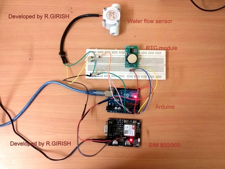 Please note that at the time of water arrival the water must free flow, meaning if there is any block or tap which is closed will not notify you.
If you have any questions regarding this project, feel free to express in the comment section, you may receive a quick reply.
Please note that at the time of water arrival the water must free flow, meaning if there is any block or tap which is closed will not notify you.
If you have any questions regarding this project, feel free to express in the comment section, you may receive a quick reply.
 A 25 watt bulb acts as heat source; higher wattage may hurt the eggs in a small container.
The humidity is provided by vaporizer, you may use the vaporizer something similar as shown below.
A 25 watt bulb acts as heat source; higher wattage may hurt the eggs in a small container.
The humidity is provided by vaporizer, you may use the vaporizer something similar as shown below.
 It produces thick stream of steam which will be inlet to incubator.
The steam can be carried via any flexible tube.
The flexible tube can be something similar as shown below:
It produces thick stream of steam which will be inlet to incubator.
The steam can be carried via any flexible tube.
The flexible tube can be something similar as shown below:
 The steam may be inlet from top of the Styrofoam / thermocol box as shown in the apparatus design, so that excess heat will escape though the humidity control holes and less hurting the eggs.
There is a cylinder carrying eggs with several holes around it, connected to a servo motor.
The servo motor rotates the cylinder 180 degree every 8 hours thus rotates the eggs.
The rotation of the eggs prevents the embryo sticking to the shell membrane and also provides contact with the food material in the egg, especially at early stage of incubation.
The rotating cylinder must have several numbers of holes so that proper air circulation will be present and also the cylinder must be hollow on both sides.
The rotating cylinder can be PVC tube or cardboard cylinder.
Paste an ice cream stick on both end of the hollow cylinder such that the ice cream stick makes two equal semi circles.
Paste the arm of the servo motor at middle of the ice cream stick.
On the other side poke a hole and paste a tooth pick firmly.
Insert the tooth pick inside box and paste the servo on opposite wall inside the box.
The cylinder must stay horizontal as possible, now the cylinder can rotate as the servo motor rotates.
And yes, use your creativity to make the things better.
If you want to accommodate more eggs make more such cylinders and multiple servo motor can be connected on same control line pin.
The humidity control holes can be made by poking a pencil through the Styrofoam / thermocol box at the top.
If you made lot of unnecessary holes or if humidity or temperature is escaping too fast you may cover some of the holes using electrical or duct tape.
The DHT11 sensor is heart of the project which may be placed at the middle of any four sides of incubator (inside) but away from the bulb or humidity inlet tube.
CPU fans can be placed as shown in the apparatus design for air circulation.
For proper air circulation use at-least two fans pushing the air in opposite direction, for example: one of the CPU fan pushing downwards and another CPU fan pushing upwards.
Most CPU fan works on 12V but at 9V works just fine.
That¡¯s all about the apparatus.
Now let¡¯s discuss on the circuit.
The steam may be inlet from top of the Styrofoam / thermocol box as shown in the apparatus design, so that excess heat will escape though the humidity control holes and less hurting the eggs.
There is a cylinder carrying eggs with several holes around it, connected to a servo motor.
The servo motor rotates the cylinder 180 degree every 8 hours thus rotates the eggs.
The rotation of the eggs prevents the embryo sticking to the shell membrane and also provides contact with the food material in the egg, especially at early stage of incubation.
The rotating cylinder must have several numbers of holes so that proper air circulation will be present and also the cylinder must be hollow on both sides.
The rotating cylinder can be PVC tube or cardboard cylinder.
Paste an ice cream stick on both end of the hollow cylinder such that the ice cream stick makes two equal semi circles.
Paste the arm of the servo motor at middle of the ice cream stick.
On the other side poke a hole and paste a tooth pick firmly.
Insert the tooth pick inside box and paste the servo on opposite wall inside the box.
The cylinder must stay horizontal as possible, now the cylinder can rotate as the servo motor rotates.
And yes, use your creativity to make the things better.
If you want to accommodate more eggs make more such cylinders and multiple servo motor can be connected on same control line pin.
The humidity control holes can be made by poking a pencil through the Styrofoam / thermocol box at the top.
If you made lot of unnecessary holes or if humidity or temperature is escaping too fast you may cover some of the holes using electrical or duct tape.
The DHT11 sensor is heart of the project which may be placed at the middle of any four sides of incubator (inside) but away from the bulb or humidity inlet tube.
CPU fans can be placed as shown in the apparatus design for air circulation.
For proper air circulation use at-least two fans pushing the air in opposite direction, for example: one of the CPU fan pushing downwards and another CPU fan pushing upwards.
Most CPU fan works on 12V but at 9V works just fine.
That¡¯s all about the apparatus.
Now let¡¯s discuss on the circuit.
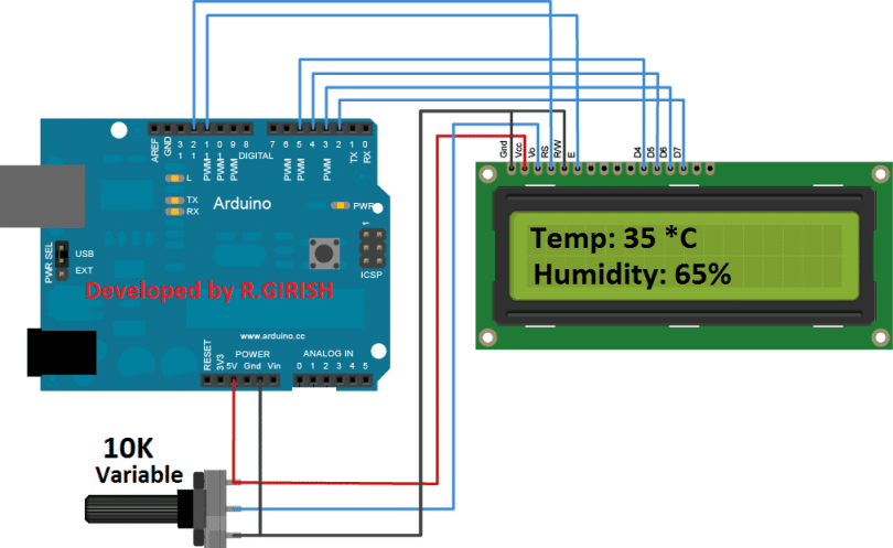 The above circuit is for Arduino to LCD connection.
Adjust 10K potentiometer for adjusting LCD contrast.
The above circuit is for Arduino to LCD connection.
Adjust 10K potentiometer for adjusting LCD contrast.
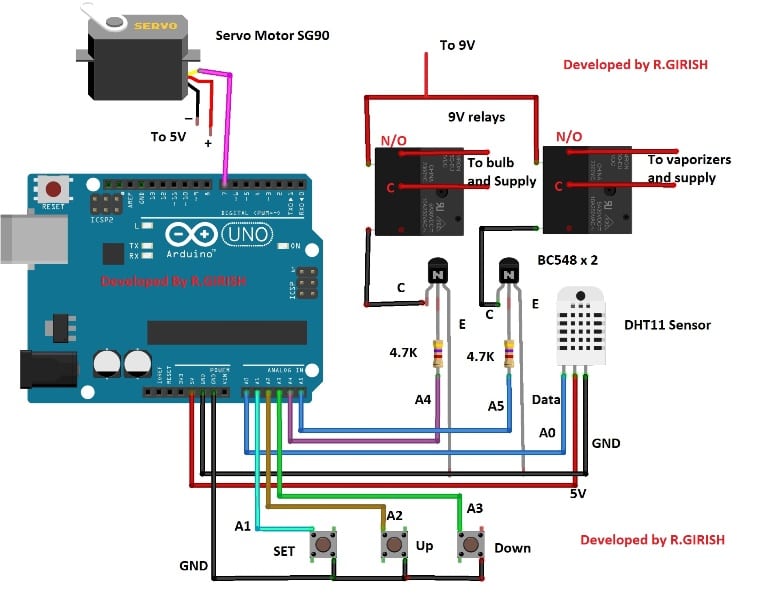 The Arduino is the brain of the project.
There are 3 push buttons for setting temperature and humidity.
The pin A5 controls the relay for vaporizer and A4 for the bulb.
The DHT11 sensor is connected to pin A0. The pins A1, A2 and A3 used for push buttons.
The pin #7 (non-PWM pin) is connected to servo motor¡¯s control wire; multiple servo motors can be connected to pin #7. There is misconception that servo motors works only with PWM pins of Arduino, which is not true.
It works happily on non PWM pins too.
Connect a diode 1N4007 across the relay coil in reverse bias to eliminate high voltage spikes while switching on and off.
The Arduino is the brain of the project.
There are 3 push buttons for setting temperature and humidity.
The pin A5 controls the relay for vaporizer and A4 for the bulb.
The DHT11 sensor is connected to pin A0. The pins A1, A2 and A3 used for push buttons.
The pin #7 (non-PWM pin) is connected to servo motor¡¯s control wire; multiple servo motors can be connected to pin #7. There is misconception that servo motors works only with PWM pins of Arduino, which is not true.
It works happily on non PWM pins too.
Connect a diode 1N4007 across the relay coil in reverse bias to eliminate high voltage spikes while switching on and off.
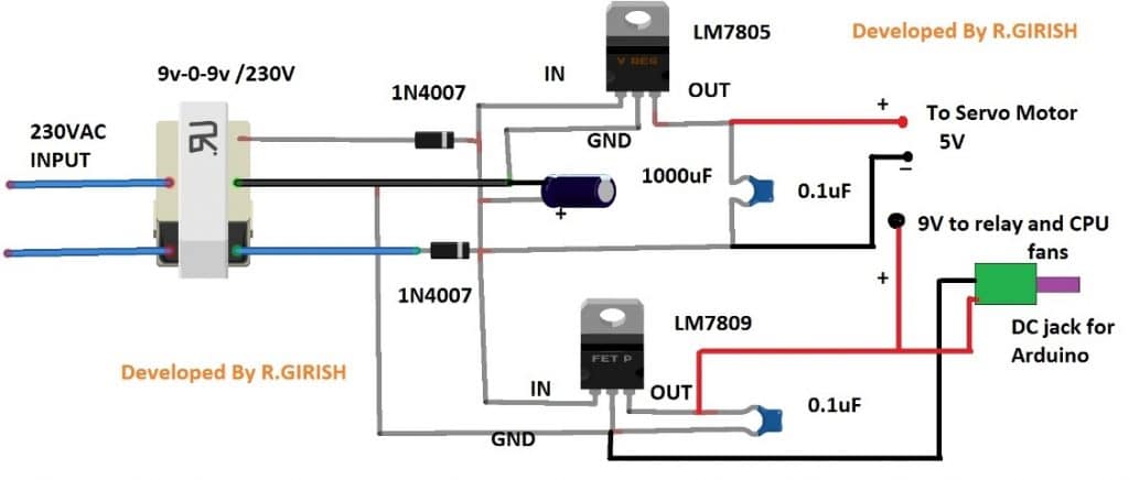 The above power supply can provide 9 V and 5 V supply for relay, Arduino, Servo motor (SG90) and CPU fans.
The DC jack is provided for powering the Arduino.
Use heat sinks for the voltage regulators.
That concludes the power supply.
Download the library DHT sensor:
https://arduino-info.wikispaces.com/file/detail/DHT-lib.zip
The above power supply can provide 9 V and 5 V supply for relay, Arduino, Servo motor (SG90) and CPU fans.
The DC jack is provided for powering the Arduino.
Use heat sinks for the voltage regulators.
That concludes the power supply.
Download the library DHT sensor:
https://arduino-info.wikispaces.com/file/detail/DHT-lib.zip
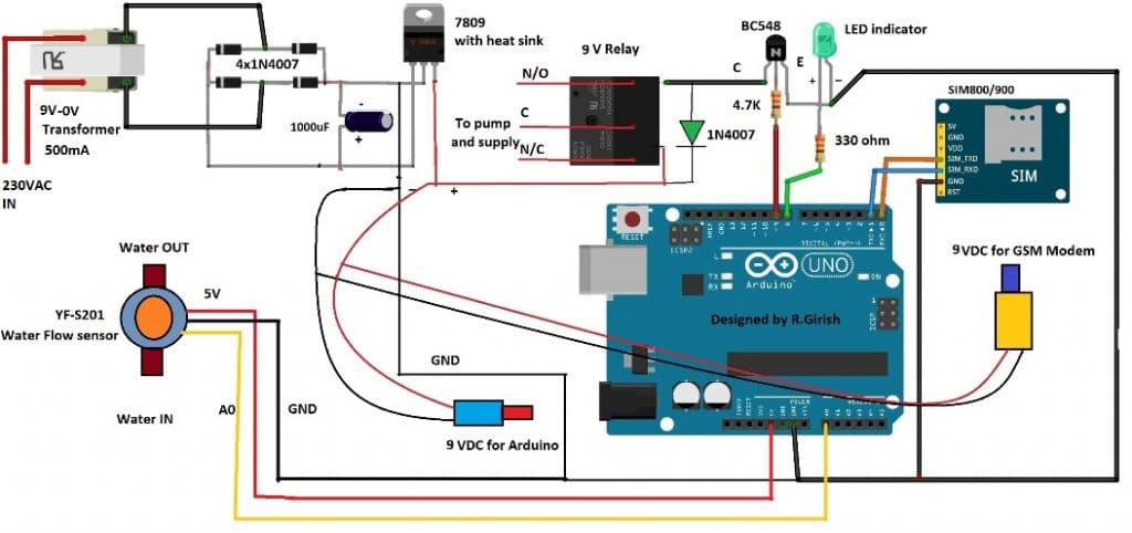 The circuit consists of AC to DC converter using 9V transformer, bridge rectifier a smoothing capacitor of 1000 uF and a LM7809 9V regulator.
Two DC jacks are provided for powering Arduino board and SIM 800 / SIM 900 GSM module.
Never power the GSM module with 5V pin of Arduino to 5V pin of GSM module as the Arduino board cannot provide enough current.
The connection between Arduino and GSM module as follows:
Arduino TX ---------------------- RX SIM 800 / 900
Arduino RX --------------------- TX SIM 800 / 900
Arduino GND ------------------- GND SIM 800 / 900
The main supply is provided by the LM 7809 regulator.
The LED indicator will glow if the relay is activated and turns off when the relay is deactivated.
The diode IN4007 will absorbed high voltage spike which occurs while switching the relay on and off.
The water flow sensor is connected to A0 pin of Arduino, 5V and GND provided from Arduino board.
The circuit consists of AC to DC converter using 9V transformer, bridge rectifier a smoothing capacitor of 1000 uF and a LM7809 9V regulator.
Two DC jacks are provided for powering Arduino board and SIM 800 / SIM 900 GSM module.
Never power the GSM module with 5V pin of Arduino to 5V pin of GSM module as the Arduino board cannot provide enough current.
The connection between Arduino and GSM module as follows:
Arduino TX ---------------------- RX SIM 800 / 900
Arduino RX --------------------- TX SIM 800 / 900
Arduino GND ------------------- GND SIM 800 / 900
The main supply is provided by the LM 7809 regulator.
The LED indicator will glow if the relay is activated and turns off when the relay is deactivated.
The diode IN4007 will absorbed high voltage spike which occurs while switching the relay on and off.
The water flow sensor is connected to A0 pin of Arduino, 5V and GND provided from Arduino board.
 The following things we can observe from the screen shot:
¡¤ First the motor is turned on and the circuit acknowledged with a reply.
¡¤ The motor is deactivated and the circuit is acknowledged with a reply.
¡¤ Again the motor is activated and unplugged the sensor to simulate dry run situation, the circuit turns the pump off and replied with pump dry run acknowledgement.
¡¤ Finally a test SMS has sent and the circuit replied with ¡°System is Working Fine¡±.
I would suggest installing the water flow sensor after couple of meters after the water pump.
That concludes the GSM based pump dry run preventer.
Now let¡¯s take a look at simple water pump dry run preventer without GSM, this could be the easier of the two.
The following things we can observe from the screen shot:
¡¤ First the motor is turned on and the circuit acknowledged with a reply.
¡¤ The motor is deactivated and the circuit is acknowledged with a reply.
¡¤ Again the motor is activated and unplugged the sensor to simulate dry run situation, the circuit turns the pump off and replied with pump dry run acknowledgement.
¡¤ Finally a test SMS has sent and the circuit replied with ¡°System is Working Fine¡±.
I would suggest installing the water flow sensor after couple of meters after the water pump.
That concludes the GSM based pump dry run preventer.
Now let¡¯s take a look at simple water pump dry run preventer without GSM, this could be the easier of the two.
 Nothing much about to explain here, just wire up as per the schematic.
The power supply can be a 9V wall adapter with at-least 500 mA or the supply which illustrated in the GSM based controller schematic.
The push button is provided to turn the pump on and off.
Once you press the button to turn on the pump, the circuit waits till 20 seconds initially to detect the flow of water, during that time the push button is disabled for 20 seconds.
After the initial 20 seconds the push button is enabled and you may turn OFF the pump manually by pressing the push button again.
If water flow is detected the circuit keeps the pump ON after 20 seconds, otherwise the circuit cuts the power supply to the motor.
Also the circuit can cut off the supply at any instant, if no water flow detected.
If the circuit shut off due to dry run, the LED blinks rapidly.
Nothing much about to explain here, just wire up as per the schematic.
The power supply can be a 9V wall adapter with at-least 500 mA or the supply which illustrated in the GSM based controller schematic.
The push button is provided to turn the pump on and off.
Once you press the button to turn on the pump, the circuit waits till 20 seconds initially to detect the flow of water, during that time the push button is disabled for 20 seconds.
After the initial 20 seconds the push button is enabled and you may turn OFF the pump manually by pressing the push button again.
If water flow is detected the circuit keeps the pump ON after 20 seconds, otherwise the circuit cuts the power supply to the motor.
Also the circuit can cut off the supply at any instant, if no water flow detected.
If the circuit shut off due to dry run, the LED blinks rapidly.


 Make connections as shown in circuit diagram.
1. Connect end terminals of potentiometer to 5v pin and ground pin of arduino UNO respectively whereas its wiper terminal to pin analog pin A1.
2. Connect PWM pin 6 of arduino to the base of mosfet.
3. Positive terminal of battery to drain of mosfet and negative to p-terminal of schottky diode.
4. From p-terminal of schottky diode, connect load (motor) in series with inductor to source terminal of mosfet.
5. Now connect n-terminal of schottky diode to source terminal of mosfet.
6. Connect 47uf capacitor across motor.
7. At last connect ground pin of arduino to the source terminal of mosfet.
Make connections as shown in circuit diagram.
1. Connect end terminals of potentiometer to 5v pin and ground pin of arduino UNO respectively whereas its wiper terminal to pin analog pin A1.
2. Connect PWM pin 6 of arduino to the base of mosfet.
3. Positive terminal of battery to drain of mosfet and negative to p-terminal of schottky diode.
4. From p-terminal of schottky diode, connect load (motor) in series with inductor to source terminal of mosfet.
5. Now connect n-terminal of schottky diode to source terminal of mosfet.
6. Connect 47uf capacitor across motor.
7. At last connect ground pin of arduino to the source terminal of mosfet.
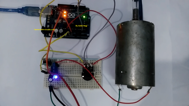
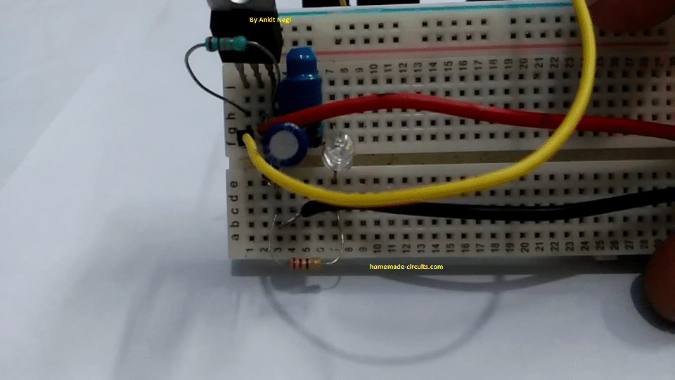

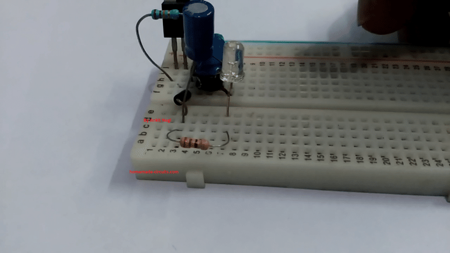 Video Clip of the above Explained Buck Converter Circuit using Arduino
 YF-S201 is a Hall Effect based water sensor.
It has three terminals 5V (nominal working voltage), GND and output.
The +5V is red coloured wire, the black one is GND and yellow one is output.
The sensor gives out frequency directly proportional to water flow.
The YF-S201 sensor can measure from 1 litre / minute to 30 litre / minute.
The water pressure should be less than or equal to 1.75 MPa.
The water can be injected from one end and water flows through the other end.
The sensor may be placed after the main gate-valve of tank; if you want to measure the water flow in a network of water pipes or you can place just before a water tap to measure the water flow of single tap.
The placement of the sensor can be anywhere according to user¡¯s need but, care must be taken to avoid leakage of water.
The sensor has a magnet and Hall Effect sensor; if we take a look at the sides of the water flow sensor, we can witness a plastic turbine in the path of water flow.
A round shaped magnet is embedded at the center of the turbine and the Hall Effect sensor is sealed and protected from moisture and placed above the magnet.
The Hall Effect sensor produces a pulse for every revolution of the turbine.
YF-S201 is a Hall Effect based water sensor.
It has three terminals 5V (nominal working voltage), GND and output.
The +5V is red coloured wire, the black one is GND and yellow one is output.
The sensor gives out frequency directly proportional to water flow.
The YF-S201 sensor can measure from 1 litre / minute to 30 litre / minute.
The water pressure should be less than or equal to 1.75 MPa.
The water can be injected from one end and water flows through the other end.
The sensor may be placed after the main gate-valve of tank; if you want to measure the water flow in a network of water pipes or you can place just before a water tap to measure the water flow of single tap.
The placement of the sensor can be anywhere according to user¡¯s need but, care must be taken to avoid leakage of water.
The sensor has a magnet and Hall Effect sensor; if we take a look at the sides of the water flow sensor, we can witness a plastic turbine in the path of water flow.
A round shaped magnet is embedded at the center of the turbine and the Hall Effect sensor is sealed and protected from moisture and placed above the magnet.
The Hall Effect sensor produces a pulse for every revolution of the turbine.
 We have blown air through the sensor to rotate the turbine as a test and the waveform generated is shown above.
The denser waveform on left hand side represents higher frequency and faster rotation of turbine, the less dense waveform at right hand side signifies the vice versa.
A consistent water flow gives out consistent frequency output.
We have to convert the frequency into litre/minute scale.
To do this, the manufacturer has given a formula:
We have blown air through the sensor to rotate the turbine as a test and the waveform generated is shown above.
The denser waveform on left hand side represents higher frequency and faster rotation of turbine, the less dense waveform at right hand side signifies the vice versa.
A consistent water flow gives out consistent frequency output.
We have to convert the frequency into litre/minute scale.
To do this, the manufacturer has given a formula:
 The water flow sensor¡¯s output pin is connected to A0 of Arduino.
Use the 10K potentiometer for adjusting display contrast.
Wire the Arduino and LCD display as per the above diagram.
The water flow sensor¡¯s output pin is connected to A0 of Arduino.
Use the 10K potentiometer for adjusting display contrast.
Wire the Arduino and LCD display as per the above diagram.
 The ¡°L/Min¡± indicates the current water flow rate and the ¡°Total¡± indicates the total water flowed since the circuit turned ON.
You can also flow any liquids whose viscosity value is near to water.
If you have any questions regarding this digital water flow meter using Arduino, feel free to express in the comment section, you may receive a quick reply.
The ¡°L/Min¡± indicates the current water flow rate and the ¡°Total¡± indicates the total water flowed since the circuit turned ON.
You can also flow any liquids whose viscosity value is near to water.
If you have any questions regarding this digital water flow meter using Arduino, feel free to express in the comment section, you may receive a quick reply.


 The pin connections for NRF24L01 module and joystick is provided in the diagram, if you feel any muddle, please refer the given pin connection table.
By moving the joystick forward (UP), reverse (Down), right and left, the car moves accordingly.
The pin connections for NRF24L01 module and joystick is provided in the diagram, if you feel any muddle, please refer the given pin connection table.
By moving the joystick forward (UP), reverse (Down), right and left, the car moves accordingly.

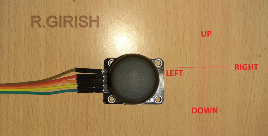 Please note that all the wire connections are at left side, this is the reference point and now you can move the joystick to move the car.
By pressing the joystick in Z axis you can control the LED light on the car.
Please note that all the wire connections are at left side, this is the reference point and now you can move the joystick to move the car.
By pressing the joystick in Z axis you can control the LED light on the car.

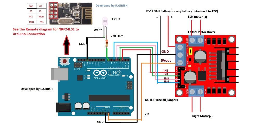 Please note that connection between Arduino board and NRF24L01 are NOT shown in the above diagram for avoiding wiring confusion.
Please refer the remote¡¯s schematic.
The Arduino board will be powered by L298N module; it has built in 5V regulator.
The white LED may be placed as head light or you can customize this pin to your needs, by pressing the joystick, the pin #7 turns high and pressing the joystick again will turns the pin low.
Please note that connection between Arduino board and NRF24L01 are NOT shown in the above diagram for avoiding wiring confusion.
Please refer the remote¡¯s schematic.
The Arduino board will be powered by L298N module; it has built in 5V regulator.
The white LED may be placed as head light or you can customize this pin to your needs, by pressing the joystick, the pin #7 turns high and pressing the joystick again will turns the pin low.

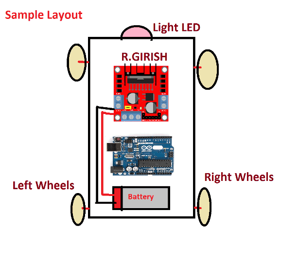 Please pay attention to the left and right side motors specified in the receiver schematic diagram.

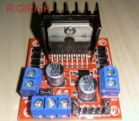 The module is built around IC L298N; it is commonly available at E-commerce websites.
We use DC motor drivers because the ICs and microcontrollers are not capable of delivering current not more than 100 milliamps in general.
The microcontrollers are smart but not strong; this module will add some muscles to Arduino, ICs and other microcontrollers to drive high power DC motors.
It can control 2 DC motors simultaneously up to 2 amps each or one stepper motor.
We can control the speed using PWM and also its rotational direction of the motors.
This module is ideal for building robots and land moving projects such as toy cars.
Let¡¯s see the technical details of L298N module.
The module is built around IC L298N; it is commonly available at E-commerce websites.
We use DC motor drivers because the ICs and microcontrollers are not capable of delivering current not more than 100 milliamps in general.
The microcontrollers are smart but not strong; this module will add some muscles to Arduino, ICs and other microcontrollers to drive high power DC motors.
It can control 2 DC motors simultaneously up to 2 amps each or one stepper motor.
We can control the speed using PWM and also its rotational direction of the motors.
This module is ideal for building robots and land moving projects such as toy cars.
Let¡¯s see the technical details of L298N module.

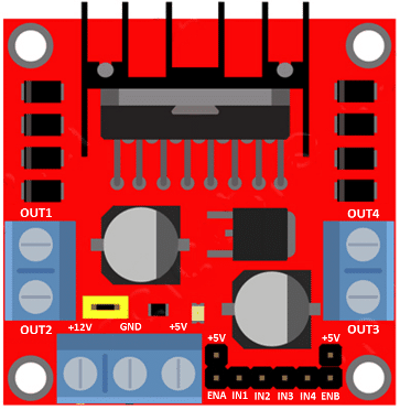

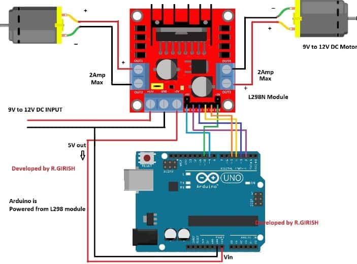 The above circuit can be used for toy cars, if you change the code appropriately and add a joystick.
You just need to power the L289N module and the module will power the Arduino via Vin terminal.
The above circuit will rotate the both motors clock-wise for 3 second and stop for 3 second.
After that the motor will rotate anti-clockwise for 3 seconds and stop for 3 seconds.
This demonstrates the H-bridge in action.
After that both the motor will start rotating slowly in anti-clockwise gaining speed gradually to maximum and gradually reduce the speed to zero.
This demonstrates speed control of motors by PWM.
The above circuit can be used for toy cars, if you change the code appropriately and add a joystick.
You just need to power the L289N module and the module will power the Arduino via Vin terminal.
The above circuit will rotate the both motors clock-wise for 3 second and stop for 3 second.
After that the motor will rotate anti-clockwise for 3 seconds and stop for 3 seconds.
This demonstrates the H-bridge in action.
After that both the motor will start rotating slowly in anti-clockwise gaining speed gradually to maximum and gradually reduce the speed to zero.
This demonstrates speed control of motors by PWM.

 If you have any questions regarding this L298N DC motor driver project, feel free to express in the comment section, you may receive a quick reply.
 The above schematic is for interfacing the Arduino and TCS3200 colour sensor.
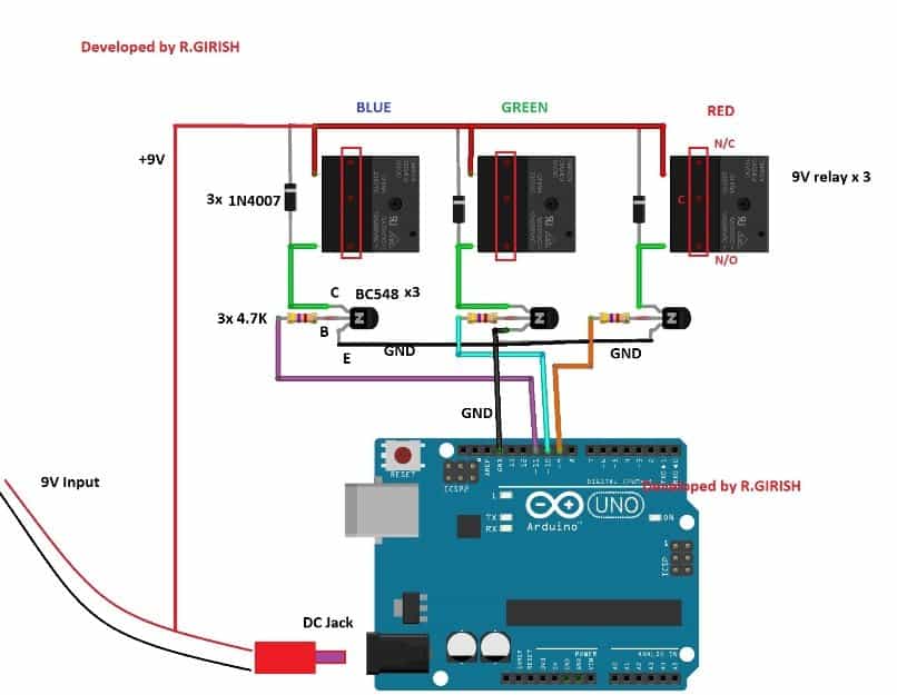 Power the Arduino with 9V adapter with at least 500mA.
The transistor acts as amplifier for relay since the Arduino¡¯s GPIO pins cannot provide sufficient current to relay.
The diode 1N4007 will absorb high voltage spikes from relay coil, protecting rest of the semiconductor components.
That concludes the hardware.
Now let¡¯s see how to upload the code and calibrate the sensor for your requirements.
The color sensitivity can vary from module to module and ambient light can alter the color sensitivity drastically.
All the TCS3200 sensors have some variation while fabricating, you have to measure the color parameters for the sensor which you currently own, so that those parameters can be used in the code to detect the color more accurately.
To calibrate and optimize the readings for your sensor follow, the steps precisely:
Power the Arduino with 9V adapter with at least 500mA.
The transistor acts as amplifier for relay since the Arduino¡¯s GPIO pins cannot provide sufficient current to relay.
The diode 1N4007 will absorb high voltage spikes from relay coil, protecting rest of the semiconductor components.
That concludes the hardware.
Now let¡¯s see how to upload the code and calibrate the sensor for your requirements.
The color sensitivity can vary from module to module and ambient light can alter the color sensitivity drastically.
All the TCS3200 sensors have some variation while fabricating, you have to measure the color parameters for the sensor which you currently own, so that those parameters can be used in the code to detect the color more accurately.
To calibrate and optimize the readings for your sensor follow, the steps precisely:
 Bring the color object (colored paper is preferred) red, blue and green.
 You have press reset button on Arduino board to deactivate the relay.
NOTE 1: The circuit may not detect the colors, if you place slightly different shade/tint of RED, GREEN, BLUE colored object/paper, after calibration.
In other words, you have to use exactly same colored object/paper to detect colors and to trigger relay.
NOTE 2: Ambient light can affect the color detection so, please maintain a consistent light near the sensor while calibrating and also while detecting colors.
You have press reset button on Arduino board to deactivate the relay.
NOTE 1: The circuit may not detect the colors, if you place slightly different shade/tint of RED, GREEN, BLUE colored object/paper, after calibration.
In other words, you have to use exactly same colored object/paper to detect colors and to trigger relay.
NOTE 2: Ambient light can affect the color detection so, please maintain a consistent light near the sensor while calibrating and also while detecting colors.
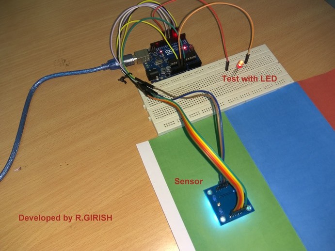 If you have any questions regarding this project, please express in the comment section, you may receive a quick reply.
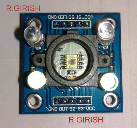 It has 4 built in white LEDs for illuminating the object.
It has 10 pins; two Vcc and GND pins (use any two of these).
The function of S0, S1, S2, S3, S4 and ¡®out¡¯ pin will be explained shortly.
If take a close look at the sensor, we can see something as illustrated below:
It has 4 built in white LEDs for illuminating the object.
It has 10 pins; two Vcc and GND pins (use any two of these).
The function of S0, S1, S2, S3, S4 and ¡®out¡¯ pin will be explained shortly.
If take a close look at the sensor, we can see something as illustrated below:
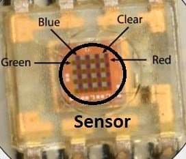 It has 8 x 8 array of color sensor that¡¯s total of 64. The photo-sensors block has Red, Blue, Green sensors.
The different color sensors are formed by applying different color filters on the sensor.
Out of 64, it has 16 blue, 16 green, 16 red sensors and there are 16 photo sensors without any color filter.
The blue color filter will allow only blue colored light to hit the sensor and reject the rest of the wavelengths (Colors); this is same for other two color sensors.
If you shine a blue light on a red filter or green filter, less intense light will pass through the green or red filters compare to blue filter.
So the blue filtered sensor will receive more light compare to other two.
So, we can put the colour sensors with RGB filters in a block and shine any coloured light, and the relevant colour sensor will receive more light than other two.
By measuring the intensity of the light received at a sensor can reveal the colour the light shined.
To interface the signal from sensor to microcontroller is done with light intensity to frequency converter.
It has 8 x 8 array of color sensor that¡¯s total of 64. The photo-sensors block has Red, Blue, Green sensors.
The different color sensors are formed by applying different color filters on the sensor.
Out of 64, it has 16 blue, 16 green, 16 red sensors and there are 16 photo sensors without any color filter.
The blue color filter will allow only blue colored light to hit the sensor and reject the rest of the wavelengths (Colors); this is same for other two color sensors.
If you shine a blue light on a red filter or green filter, less intense light will pass through the green or red filters compare to blue filter.
So the blue filtered sensor will receive more light compare to other two.
So, we can put the colour sensors with RGB filters in a block and shine any coloured light, and the relevant colour sensor will receive more light than other two.
By measuring the intensity of the light received at a sensor can reveal the colour the light shined.
To interface the signal from sensor to microcontroller is done with light intensity to frequency converter.
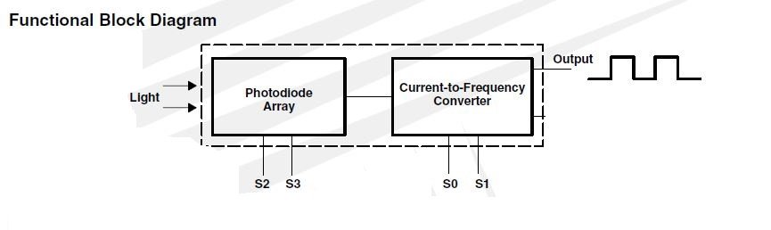 The ¡°out¡± pin is the output.
The output pin¡¯s frequency is 50% duty cycle.
S2 and S3 pins are select lines for photo-sensor.
You understand better by looking the tabulation:
The ¡°out¡± pin is the output.
The output pin¡¯s frequency is 50% duty cycle.
S2 and S3 pins are select lines for photo-sensor.
You understand better by looking the tabulation:
 By applying low signals to pin S2 and S3 will select the red colour sensor and measure the intensity of red wavelength.
Similarly, follow the above tabulation for rest of the colors.
In general Red, blue and green sensors are measured leaving the sensors one without filters.
The S0 and S1 are the frequency scaling pins:
By applying low signals to pin S2 and S3 will select the red colour sensor and measure the intensity of red wavelength.
Similarly, follow the above tabulation for rest of the colors.
In general Red, blue and green sensors are measured leaving the sensors one without filters.
The S0 and S1 are the frequency scaling pins:
 S0 and S1 are frequency scaling pins to scale the output frequency.
The frequency scaling is used to select the optimum output frequency from sensor to the microcontroller.
In case of Arduino 20% is recommended, S0 ¡®HIGH¡¯ and S1 ¡®LOW¡¯.
The output frequency goes high if the light intensity of the relevant sensor is high.
For simplicity of the program code the frequency is not measured, but the pulse duration is measured, higher the frequency less the pulse duration.
So, the one which on the serial monitor readings shows the least has to be the color which is placed in front of sensor.
S0 and S1 are frequency scaling pins to scale the output frequency.
The frequency scaling is used to select the optimum output frequency from sensor to the microcontroller.
In case of Arduino 20% is recommended, S0 ¡®HIGH¡¯ and S1 ¡®LOW¡¯.
The output frequency goes high if the light intensity of the relevant sensor is high.
For simplicity of the program code the frequency is not measured, but the pulse duration is measured, higher the frequency less the pulse duration.
So, the one which on the serial monitor readings shows the least has to be the color which is placed in front of sensor.

 The reading one which shows the lowest is the colour placed in front of the sensor.
You may also write code for recognizing any colour for example yellow.
Yellow is the result of blending of green and red, so if yellow colour is placed in front of the sensor, you have to take the red and green sensor readings into consideration, similarly for any other colours.
If you have any questions regarding this RGB color sensor TCS3200 using Arduino article, please express in the comment section.
You may receive a quick reply.
The above explained color sensor can be also used for triggering an external gadget though a relay for executing a desired operation.
The reading one which shows the lowest is the colour placed in front of the sensor.
You may also write code for recognizing any colour for example yellow.
Yellow is the result of blending of green and red, so if yellow colour is placed in front of the sensor, you have to take the red and green sensor readings into consideration, similarly for any other colours.
If you have any questions regarding this RGB color sensor TCS3200 using Arduino article, please express in the comment section.
You may receive a quick reply.
The above explained color sensor can be also used for triggering an external gadget though a relay for executing a desired operation.
 The display is connected to analog pins of the arduino from A0 to A5. The display is unusually connected to analog pins (which functions same as connected to digital pins) so that keypad can be connected to digital pins (from 2 to 9).
Adjust display contrast using the 10 K ohm potentiometer.
The display is connected to analog pins of the arduino from A0 to A5. The display is unusually connected to analog pins (which functions same as connected to digital pins) so that keypad can be connected to digital pins (from 2 to 9).
Adjust display contrast using the 10 K ohm potentiometer.
 The keypad has 8 cables which should be connected to Arduino, from pin #2 to pin #9. The left most wire of keypad must go to pin #9 and connect the succeeding right to next wire of keypad to pin# 8, 7 ,6, 5, 4, 3, 2, the last or the right most wire of keypad must go to pin #2.
 You need to download and add the keypad library from the following link: github.com/Chris--A/Keypad before compiling the code.
EEPROM of Arduino microcontroller would have some random values stored initially.
We have to reset to zero, so that our main program don¡¯t get confused.
To rest EEPROM values to zero upload the below program first and then upload the main program second.
You need to download and add the keypad library from the following link: github.com/Chris--A/Keypad before compiling the code.
EEPROM of Arduino microcontroller would have some random values stored initially.
We have to reset to zero, so that our main program don¡¯t get confused.
To rest EEPROM values to zero upload the below program first and then upload the main program second.
 If you have any specific question regarding this password based AC Mains ON/OFF switch circuit project, express in the command section, you may receive a quick reply.
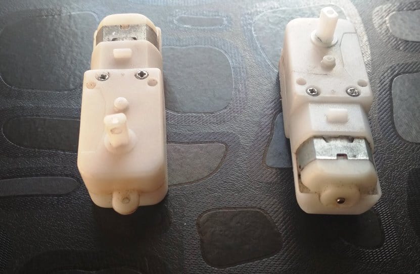 CASTOR BALL: Normal wheels provide translatory motion along a single axis but a castor ball is designed to move along any direction on surface.
It gives us three wheel drive.
The reason for preferring threewheel drive over 4 wheels is because of its comparatively faster turning action.
You might have noticed the cycle rickshaws piercing through the traffic like reptiles.
Same is the case of our robot.
CASTOR BALL: Normal wheels provide translatory motion along a single axis but a castor ball is designed to move along any direction on surface.
It gives us three wheel drive.
The reason for preferring threewheel drive over 4 wheels is because of its comparatively faster turning action.
You might have noticed the cycle rickshaws piercing through the traffic like reptiles.
Same is the case of our robot.
 SENSORS: It is a device that detects or measures any physical parameter of our environment and converts it into electric signals.
In this case the parameter detected is infra-red rays.
Sensors are highly fundamental for any robot.
Well, if arduino is our bot¡¯s brain, sensors might as well play the role of eyes.
Here are a few things about sensors:
The sensors must be oriented in a way that led(s) face the ground.
Should be placed at the front end of your bot.
Minimum spacing between them must be greater than the width of the black line.
MOTOR DRIVER BOARD : Motor-drivers are buffer circuits that take up low voltage signals to power up the motors that require higher voltage.
In our case, Arduino can provide sufficient voltage to drive the motors but it cannot provide ample current.
Arduino UNO¡¯s 5v and GND pins have current rating of 200mA while any GPIO pin has rating of 40 mA.
This is way lower than the starting and stall currents motors we need .
There are two motor drivers that I prefer for this project: L298N and L293D.
Both of them are equally suitable for making this project.
Though, L293D is comparatively cheaper but has a low current rating.
Their connections are nearly the same.
Since, I have given the connections for both, it is totally up to you how you make your bot.
SENSORS: It is a device that detects or measures any physical parameter of our environment and converts it into electric signals.
In this case the parameter detected is infra-red rays.
Sensors are highly fundamental for any robot.
Well, if arduino is our bot¡¯s brain, sensors might as well play the role of eyes.
Here are a few things about sensors:
The sensors must be oriented in a way that led(s) face the ground.
Should be placed at the front end of your bot.
Minimum spacing between them must be greater than the width of the black line.
MOTOR DRIVER BOARD : Motor-drivers are buffer circuits that take up low voltage signals to power up the motors that require higher voltage.
In our case, Arduino can provide sufficient voltage to drive the motors but it cannot provide ample current.
Arduino UNO¡¯s 5v and GND pins have current rating of 200mA while any GPIO pin has rating of 40 mA.
This is way lower than the starting and stall currents motors we need .
There are two motor drivers that I prefer for this project: L298N and L293D.
Both of them are equally suitable for making this project.
Though, L293D is comparatively cheaper but has a low current rating.
Their connections are nearly the same.
Since, I have given the connections for both, it is totally up to you how you make your bot.
 POWER SUPPLY:
Use a 12 v adapter or a battery (not more than 12 volts).
Placement of components (from front to back end):
Sensors at the head of your bot.
Castor wheel in the middle.
Motors and tyres in one line at the back.
Connections:
SENSORS to ARDUINO:
Connect the sensor pin to arduino pin as shown,
POWER SUPPLY:
Use a 12 v adapter or a battery (not more than 12 volts).
Placement of components (from front to back end):
Sensors at the head of your bot.
Castor wheel in the middle.
Motors and tyres in one line at the back.
Connections:
SENSORS to ARDUINO:
Connect the sensor pin to arduino pin as shown,
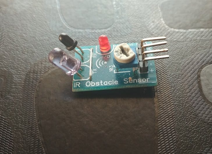
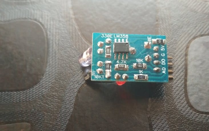
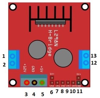
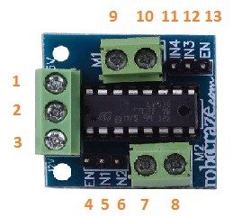

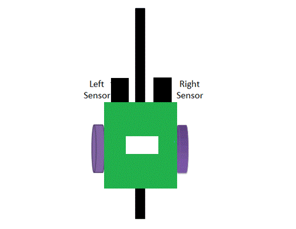 In normal condition, the robot moves in such a way that both the sensors are over white and the black line is amidst the both sensors.
It is programmed to rotate both the motors such that the bot moves in forward direction.
Quite naturally, as time elapses one of the two sensors comes over the black line.
If left sensor comes over the line, left motors are brought to rest and as a result bot begins turning towards left unless the left sensor comes back on white surface and normal condition is achieved.
Similarly, when right sensor comes over black line, right motors are stopped and consequently bot now turns towards right unless the sensor comes back over white surface.
This mechanism of turning is known as differential drive mechanism.
In normal condition, the robot moves in such a way that both the sensors are over white and the black line is amidst the both sensors.
It is programmed to rotate both the motors such that the bot moves in forward direction.
Quite naturally, as time elapses one of the two sensors comes over the black line.
If left sensor comes over the line, left motors are brought to rest and as a result bot begins turning towards left unless the left sensor comes back on white surface and normal condition is achieved.
Similarly, when right sensor comes over black line, right motors are stopped and consequently bot now turns towards right unless the sensor comes back over white surface.
This mechanism of turning is known as differential drive mechanism.

