A field strength meter is an electronic device which is used for detecting and measuring the RF radiation generated from any RF transmitter circuit.
As we all know that transmitter circuits invariably use an inductor/capacitor based LC resonating circuit, also called the tank circuit, which oscillates at a specified resonating frequency to transmit the frequency in the air with an optimum power.
A field strength meter picks up this frequency radiation from the transmitters LC antenna network, and displays its strength or power through the attached meter.
Using an FET
The first field strength meter circuit below can work withany frequency as high as250 MHz, or perhaps even more if needed.
Radio frequency energy is sensedby a short whip, rod, telescopic or other antenna, and the signal is rectifiedby diode D1 whichgives a positive voltage for the FET gate across R1.
Because this FET is solely used as a DC amplifier, a 2N3819 or some other general-purpose transistor will suffice.
The "Set Zero" potentiometer can be anywhere between 1k and 10k.
When there is no RF signal present, the gate/source potential can be adjusted such that the meter only indicates a tiny current.
In the presence of an RF field this current slowly grows in proportion to the intensity of the RF signal, which is indicated on the meter.
A 100uA metre may be used for increasedsensitivity.
An ammeter with a lesser sensitivity, for examplelike250uA, 500uA, or 1mA, can also be utilized and mightprovide you with adequate information in most cases.
A VHF choke RFCcan be used if the field strength metre is exclusively usedwithVHF.
On the other hand,a short wave RFCchoke will be most appropriate for regular use with lower frequencies.
Another Simple Field Strength Meter Design using a BJT
Anothersimple, and testedfield strength meter circuit that allows model RCfliers to confirm that their remote control transmitter is indeed transmitting.
Any concerns about whether a problem is in the receiver or transmitter are immediately cleared up.
The circuit's single active component is a transistor which serves like a regulated resistance in one of the bridge's arms of the meter.
The antennawire which is a telescopic type antennais attached to the transistor's base.
As the HF voltage at the base of the antenna rises, the transistor is driven out of balance, causing the bridge to collapse.
The current subsequently passes via R2, the mA meter, and the transistor's collector-emitter junction, indicating the field strength on the meter.
Before turning on the transmitter for the testing, make sure thatthe meter needle us carefully adjusted tozero mark,using P1.
Transmitter RF Output Power Equation
The electric field strength generated by a transmitter with an isotropic radiator could be easily computed in anidealized free space.
The following formula works well for determining the field strength emitted from a transmitter LC circuit:
E ˇÖ ˇĚ30 x P / d
Here, the electric field strength, E, is measured in volts per metre.
The transmitter power output in watts is denoted by P.
d representsthe distance in metres from the radiator.
The parameter ˇĚ30 represents the approximate value of ˇĚZ0/4¦Đ
where Z0 denotes impedance value of the free space, which is equal to 119.9169832 ¦Đ¦¸
The spacing between the transmitter and the receiver is clearly inversely related to the intensity of the electric field.
This relationship, unfortunately, is unsuitable for estimating the field strength generated by ground transmitters, because reflections and attenuation induced by structures in the vicinity of the transmitter or receiver can heavily impact the electrical field strength.
Ultrasonic Motion Detector Circuit
This ultrasonic motion detector circuit project picks up movement of any object including human beings from a distance of 4 to 7 meters away.
As soon as the motion is detected, the output of the circuit illuminates a red LED indicating the presence of an obstacle or an intruder.
However, using supplemental circuit stages connected to the output of the detector circuit, the device can be designed to switch on lamps, alarms, trigger a recording device, or maybe contact law enforcement.
Furthermore, the circuit could be designed to play a message whenever a person or an intruder is detected moving across its range of detection.
The circuit diagram for the Ultrasonic Motion Detector can be witnessed in the following figure.
A 9 V PP3 battery, B1, instantly supplies electrical power for a few stages of the circuit.
The battery can be also seen attached with a 78L05 regulator, IC3, that supplies a 5 V DC supply to various other stages of the circuit.
The Transmitter
The transmitter stage is essentially a crystal controlled relaxation oscillator developed using a 4049 CMOS HEX inverter, IC2. One of the IC 4049 portions, IC2c, together with resistors R21 and R22, and capacitors C11 and C12, "strikes" the 40 kHz crystal to force it into a continuous oscillating state.
The rest of the IC 4049 sections behave like linear buffers to operate a 40 kHz, ultrasonic transducer device, BZ2.
The Receiver
The receiver stage consists of 4 AC coupled sections, each one constructed using one of the four op amps from the IC LM324. In the 1st stage, the input voltage created around R1 and R2 is modulated through a 40 kHz, ultrasonic receiver transducer, BZ1, and the modulated signal is subsequently sent to the IC1a, where the frequency is amplified.
The receiver transducer picks up any kind of reflected frequency generated by the transmitter transducer, BZ2.
In case there isn't any motion, the resulting envelope signal waveform is simply produced in the form of a straight line.
Diode D1 and resistor R8 work like a negative peak detector to extract the envelope signal.
The second stage is configured around the IC1b, which amplifies the extracted signal again.
The IC1b time constant is pretty sluggish which ensures that the envelope signal can be easily tracked.
The output generated from the second stage is a voltage level which determines the strength of the envelope.
In the presence of a movement in front of the transducers, the envelope reflects the signal through a positive or negative beams.
Differential Amplifier (Window Detector)
At the third stage input we can find a differential amplifier configured around the IC1c and using a couple of diodes, D2 and D3. This stage picks up each of those positive and negative pulses.
In the absence of a motion in front of the ultrasonic sensors, the pin 7 potential of IC1b is 50 percent of the supply voltage which prevents both the diodes D2 or D3 from conducting.
The pin 8 potential of IC1c is as a result remains low.
In case the signal strength increases over +0.7 volt (breakdown voltage of a silicon diode), causes the diode D3 become forward biased and conduct, enabling pin 8 of ICc to go high.
If the reflected motion signal drops under -0.7 volt, D2 gets forward biased and begins conducting, which in turn results in the output going high.
Thus, the configuration works like a window detector.
It detects voltage levels of the reflected signals moving either below or over a specified range.
The Monostable Flip-Flop
The 4rth stage of this ultrasonic motion detector circuit is structured around IC1d.
This stage is configured like a monostable flip-flop.
This section of the circuit converts any signal which enters via the filter into a pulse, which is big enough to trigger ON transistor Q1.
As soon as the BJT Q1 activates, LED1 illuminates, and it also generates an output voltage which can be used to operate an attached relay stage or some other alarm device hooked up with the collector of Q1.
The time delay provided by this IC1d monostable flip-flop is approximately half a second which is determined by the capacitor C8 and the resistor R18. The role of the diode D4 is to separate the charge/discharge time constants.
This allows the circuit to activate instantly as soon as a movement is detected in front of the ultrasonic transducers, and additionally ensures around a 1/2 second delay for the resetting action.
About 40 kHz Ultrasonic Transducers
In the first diagram for the ultrasonic motion detector, we can see two transducers with the symbols BZ1 and BZ2. Both are 40 kHz type ultrasonic transducers.
BZ1 is the receiver transducer, while the BZ2 is the transmitter transducer.
You must make sure that the two transducers are correctly matched, and therefore buy them only as a paired units.
A matched transmitter/receiver 40 kHz transducer pair will have the respective initials printed on the back of their bodies, as shown in the following image.
The transmitter device will have the suffix T printed at the backside, while the receiver unit will have the suffix R printed on the pinout side of the body.
How to Set Up
Switch on ultrasonic motion detector circuit prferably through a fixed DC regulated power supply adapter.
Install the circuit inside a noiseless room with nothing moving around in front of the sensors BZ1/BZ2.
Even warm air shuffling or, wind blowing, or amazingly, somebody chatting loudly could activate the motion detector, if the sensitivity adjustment is fixed to its maximum limit.
After powering the circuit, allow the device to settle down for a minimum of 20 seconds to ensure the whole circuit will "calm down" electrically.
Adjust the 1M trimmer potentiometer to approximately 4 k ohms through your vision (put simply, assume the potentiometer is made up of settings starting from zero through ten, so now imagine setting it at the mark four).
At the downward adjustment of around 3 k ohms, the circuit will be most probably rendered too sensitive and might self-trigger.
You may have to go through some experimentation to achieve the most appropriate setting for your specific motion detection requirements.
PCB Design
How to Use Diodes, Transistors, ICs as Temperature Sensors
Normally we find thermistors being used as the sensor for detecting and monitoring temperatures in electronic circuits.
However, ordinary semiconductor components like transistors and diodes actually work better than thermitors when it comes to detecting temperature changes.
In fact, this feature happens to be one of the greatest drawbacks of semiconductor devices, whose working characteristics get severely affected as the temperatures on their body increases.
The increase in temperature causes the forward voltage characteristic of any semiconductor to proportionately decrease, and this attribute is exploited whenever a semiconductor part is configured for sensing temperatures.
These also become the perfect alternative for sensing temperatures changes, and the best aspect about semiconductor sensors is that the response to the temperature variations is pretty linear, which is not possible in thermistors.
The phenomenon occurs since the flow of voltage and the current across a pn junction in a BJT or a diode becomes greatly influenced by the surrounding temperature.
We can easily prove this through a common silicon diode, let's say by using any of the 1N400X series diodes or simply a 1N4148 diode.
Using 1N4148 Diode as Temperature Sensor
Hook up your ohmmeter prods across the anode and cathode pins of the diode such that the diode is forward biased.
Meaning attach the red probe of the meter on the anode of the diode, and the black prod on the cathode.
To be more precise, the proper connection will be the one which exhibits the minimum resistance on the x1, x10, or x100 ranges of the ohmmeter.
Check the meter reading, next use heat (the heat from your finger may be just sufficient, clip the diode between your fingers and hold it for a few seconds) and you may find the resistance slowly changing on the ohmmeter scale!
However, despite the fact that diodes can be usually applied as temperature sensors or transducers, they are generally not the one of the ideal alternatives.
Typically, a standard bipolar transistor or BJT can easily work like a much efficient temperature transducer, particularly if it is configured like a diode.
Meaning, when its collector and the base are joined together in common to work like one end of the "diode;" while the emitter of the transistor like the other end.
The VBE of the BJT or the base-emitter voltage in this situation will be critically dependent upon the collector current of the device and also the ambient or its case temperature.
Therefore, a BJT could be accustomed to create incredibly linear temperature transducers, that may effectively operate across a range of around -55ˇă C to + 125ˇă C.
Transistor Temperature Transducers
Practically all types transistors could be utilized to create approximate temperature measurements due to the transistor's relationship between the base-emitter voltage and temperature, provided the current flowing through its collector is constant.
However, a few BJTs tend to work like ideal temperature transducers compared to others.
Apparently transistors that come in metal can type packages (TO-5, and specifically the little TO-18 types) provide an improved response compared to the other variants having epoxy or plastic casing.
Furthermore, a number of BJTs exhibit an increased linearity on their VBE v Ic curve compared to others.
Figure 4 indicates a basic temperature transducer using NPN bipolar transistors.
Using MAT01 as Temperature Sensor
In this particular design, a twin transistor (a pair of matched NPN silicon transistors packaged inside a single case) like the one MAT01 is utilized.
The emitters are applied with 1 mA and 2 mA constant-current (make sure to use different emitter currents for Q1 and Q2) and the output voltage roughly around 59 ¦ĚV/ˇăK.
A differential opamp becomes necessary to enhance and increase the output voltage to some meaningful value.
It is advisable to calibrate the voltage range to 10 mV/ˇăK to ensure that an ordinary voltmeter could be employed.
To execute this with this BJT sensor, the differential opamp should possess a gain of over 167. When the output voltage reaches 10 mV/ˇăK, just about any 31/2 digit DVM could be taken to test the equivalent temperature across the transistor.
Using 2N2222 as Temperature Sensor
The accurate temperature transducer schematic displayed in the figure below, works with a ordinary op amp inverting follower configuration along with a single standard BJT like the 2N2222 with metal case.
The transistor is used like a temperature sensor probe which must have a appropriate housing like a vintage voltmeter probe grip, a small section of metal tube, and so on.
In case the concept is implemented to determine the temperature within an existing device, it could be fitted entirely inside the unit and may not require an independent housing.
Nevertheless, no matter how it is positioned, a good thermal contact with the temperature that is being mesured is utmost crucial.
Two DC voltage references are used for this application +/-6.2 volts.
Diode D1 supplies the +6.2 V reference, while diode D2 delivers the -6.2 V reference.
The +6.2 supply is coupled to the collector/base pinout of the temperature sensor BJT (Q1).
Meaning, the emitter current of Q1 is going to be linearly incremental and sensitive only to temperature chnages since the collector voltage for Q1 is held constant.
This current is boosted by op amp IC1 to a level proportional to an output potential of 100 mV/ˇăK.
Variable resistor R1 can be adjusted for the calibration process to ensure the appropriate scaling level.
Again, any common 31/2 digit DVM may work nicely for reading the temperatures, although the display unit is going to be in degrees Kelvin.
If you want to change the measurement to degrees Celsius, you must be aware of the fact that the Kelvin and Celsius scales are identical, but offset by 273 degrees (0ˇă C = 273ˇă K).
To see temperature readings in degrees Celsius, an offset realignment will be required.
Potentiometer R3 switches the temperature range of the standard design from Kelvin to Celsius through summing of the countercurrent from the -6.2 V supply, using the current from the BJT.
The potentiometer is tweaked to generate zero output from amplifier IC1 with a sample temperature on the transistor set precisely 0ˇă C.
Calibration
After the circuit is constructed it will need to be calibrated.
Start by setting up presets R1 and R3 to around the center of their individual dials.
Power ON the circuit, and hang on for around 5 to 10 minutes for the circuit to become stable at room temperature.
In the meantime, get ready an bowl of melting ice or an "ice point bath." The ice-point of water is 0ˇă C; (the temperature at which ice begins turning into water).
Use a common glass thermometer to validate 0ˇă C (or 32ˇă F) temperature of the melting ice.
As soon as the circuit is stable and the melting ice bath is all set, immerse the 2N2222 transistor into the bath and wait for around 30 seconds.
When you see the op amp output voltage is no longer changing, fine-tune potentiometer R3 to read exactly 0.00 volts on the meter.
Allow the 2N2222 sensor to remain in the bath for a couple more minutes, while you supervise the bath's temperature on the glass thrmometer to ensure that the bath temperature is consistent with the circuit meter reading.
Once you find the output voltage is fairly constant (slight bit of deviation is tolerable), take out the 2N2222 transistor and the glass thermometer and bring them back in room temperature.
As soon as the two units get stabilized back to the room temperature (this can be verified by the reading on the glass mercury thermometer, and a complementing constant reading on the circuit's output meter reading), the final steps of calibration procedure may be completed.
Alter potentiometer R3 such that the reading on meter connected to the op amp output matches with the reading on the mercury glass thermometer (you can ignore the figures on the right side of the decimal point on the meter).
Once this is completed, a 0 V output from the opamp will correspond to a 0ˇă C, a 3 V DC output indicate a 30ˇă C, and so on.
This takes place, obviously, due to the 100 mV/ˇăC scaling consideration.
An alternative of calibration could be to use a warm water bath.
Create the warm water bath by combining hot and cold water, and carry out the procedures which were discussed above for calibrating the circuit in room temperature.
Using Transistor and Diode Together
This temperature indicator design employs a transistor and a diode together in a mutually complementing mode.
The diode is kept in the ambient temperature, and the resulting voltage drop across it is used as the reference level.
The temperature detection is executed by a transistor positioned near the heat source which needs to be detected.
Therefore, the transistor T1 acts like the actual temperature detector with reference to the ambient temperature as detected by the diode.
This is implemented by comparing the base/emitter voltage of the BJT with the reference level from the junction of D1 and R1 through the preset P1.
The transistor will continue to be turned off so long as the temperature around it stays under a particular level, which can be appropriately set by P1.
The T1's base emitter voltage starts to drop by approximately 2 mV in response to every single degree Celsius rise in temperature around the BJT.
When the base emitter voltage of the transistor becomes lower than the voltage level at the wiper of P1, the transistor begins conducting, which is indicated by the gradually brightening light of the LED D2.
The R1 and R2 resistor values are dependent on the supply voltage, Ub, and could be determined using the following simple equations:
R1 = (Ub - 0.6 / 5) (result will be in kilo Ohms)
R2 = (Ub - 1.5) / 15 (the result will be in kilo Ohms)
For the best possible functionality of the design, it is crucial to ensure that the reference diode is positioned in the free air at room temperature, and surely never near the T1 or the heat source which is being monitored by the T1.
It should be kept in mind that no matter what, the absolute maximum temperature exposed on the transistor T1 must not go beyond 125ˇăC if you want to keep T1 in a proper working condition.
Using IC AD590 as Temperature Sensor
There are various precision integrated circuits or ICs that are specifically designed as temperatures sensors such as the AD590, LM35 etc.
The IC AD590 is simply a two pin IC that can be procured very cheaply in a TO-18 case and also with a unique 2-pin flat casing.
The device works like a temperature-sensitive current source and is scaled to read temperatures with roughly 1¦ĚA/ˇăK.
When current passed through the IC AD590 via a series a 1k resistor, causes voltage variation of 1 mV/ˇăK (as per Ohms Law) across the resistor, in response to the corresponding change in temperature on the AD590 device.
It maybe possible to use use the AD590 temperature sensor in many different ways.
One basic method is shown below, by connecting a series resistor of around 100 ohms.
This design is known as a 1-temperature, or 1-point, circuit.
The pot R2 can be tweaked to coincide the output voltage exactly in accordance with a standard mercury thermometer in some specified temperature.
Minor non-linear response in the device which is common in all semiconductor devices, might result in slight error at ranges far stripped away from the calibrated scale.
Another technique is to wire th¨¦ AD590 directly between a regulated +5 V reference source and the inverting input of an opamp.
The range aspect of the sensor could be set up through a feedback resistor (RF) through the formula:
Vo = (I ¦ĚA/ˇăK) (RF) (T).
We could likewise use the AD590 with a double trim-point circuit employing an op amp as explained above.
An offset current is summed up with the IC current at the inverting input of the op amp.
A couple of potentiometers could be wired up, one for controlling the offset and the other one for adjusting the gain, so that the circuit could be set up using two different temperatures, and thus minimizing the error.
Using LM35
The LM35 is another high versatile and accurate temperature sensor designed to produce an output voltage that may be directly proportional to the temperature in degrees Celsius.
This signifies that when the temperature is 0 ˇăC, the output voltage will be 0 V.
The output voltage rises through 10 mV for every single degree Celsius.
Meaning, if the LM35 temperature is 19.8 ˇăC, it will provide an output voltage of 0.198 V.
It is definitely a significant edge over other temperature sensors which are designed to generate the output in kelvin.
For these sensors measuring temperature in degrees Celsius demands an incredibly stable reference voltage that needs to be subtracted from the reading.
An additional good thing about the LM35 is its surprisingly low current consumption which is no more than 60 ¦ĚA.
This provides an extended battery life and little IC power dissipation, that ensures errors due to internal heat tend to be negligible, at around 0.1 ˇăC with a battery voltage of 4 V.
How to Connect
You can configure the LM35 sensor directly with an analogue or digital multimeter, or, more strangely enough, to a personal computer which could subsequently process and store the detected temperature data.
An appropriate software for this function can be searched online.
The reliability of the LM35/LM35C is normally 0.4 ˇăC at 25 ˇăC.
To make sure that the internal dissipation remains small, the load must be not lower than 5 k.
If an extended shielded cable is employed between the sensor and the meter, an RC configuration (a series 10 Ohm resistor with I ¦ĚF) must be attached between the output of the LM35 and the ground to protect against any kind of induced oscillations.
Automatic Light Sensitive Switch with Adjustable Dawn or Dusk Switching
This automatic ON/OFF light switch features a selector switch which facilitates the lamp (load) either to switch ON during night and switch OFF during day, or the opposite, that is switch ON during day and switch off at night or in darkness.
In other words the circuit can be used like a day activated automatic switch or a darkness activated automatic switch, depending upon the user preference or the specific application need.
The selection can be implemented simply with a flick of a DPDT switch.
WARNING: The circuit is not isolated from the AC mains supply and will be floating at the mains level, which can be fatal for anybody who touches the circuit in powered ON condition, without an insulated enclosure.
Circuit Description
Referring to the schematic above, the working of this dual function light activated switch can be understood with the following points:
The op amp 741 forms the heart of the circuit and is wired as a comparator.
Its non-inverting input pin#3 is clamped with a fix reference derived from the junction of the resistive divider formed by R2/R3.
R2, R3 being equal in value, the reference voltage is set at the 50% of the zener voltage D5 which is used for stabilizing the rectified 310 VDC to 10 V DC.
The input DC power is supplied directly from the AC mains via a bridge rectifier set up, while the rectified DC high current is dropped through R1 to suit the attached electronic circuitry.
Now, the non-inverting pin of the op amp being fixed at around 5 V reference, the inverting input pin#2 is used for the detection of the light level via another resistive network formed by R1/P1 and the LDR.
Using as Light Activated Switch
Since the pin#3 is fixed at 5 V, means, as long as the pin#2 remains below this reference level, the op amp output remains high, enabling the T1 to remain switched ON, and the SCR/load switched OFF.
This situation takes place when the R4 end is connected with the positive line, and the LDR is connected at point B which is the ground line, and illuminated by day light.
This is because, during day time the LDR resistance drops drastically causing the pin#2 potential to drop significantly and below pin#3 potential.
So with the selector switch contacts connected across points E and B, the light sensitive switch works like an automatic light activated switch.
Using as Night or Darkness Activated Switch
In order to flip the response, and enable the light sensitive switch to work like a darkness or night activated switch, we just have to toggle the selector switch such that the relevant contacts connect the points D with the positive line, and point C with the negative line.
Once this is implemented, the LDR now gets associated with the positive line, and the R4 end gets connected with the negative line.
In this situation, if the LDR is sufficiently illuminated, causes its resistance to drop, which in turn causes the pin#2 potential to rise over the pin#3 reference level.
This instantly causes the op amp output pin#6 to go logic zero, and switch OFF the BJT driver.
With the BJT turned OFF, the SCR and the load are also turned OFF in the presence of day light on the LDR.
Next, when darkness sets in, the LDR resistance increases sufficiently, causing the pin#2 potential to drop below the pin#3 potential, switching ON the BJT, the SCR, and the load, during the night time.
The circuit is now transformed into a darkness activated switch for the load or the connected lamp.
Therefore, just by flipping the selector switch connections across the B-C and D-E points, the light sensitive switch can be quickly pushed into the desired modes, either as an automatic light activated or darkness activated switch.
Hysteresis Function
Resistor R5 introduces some level of hysteresis to the op amp response so that the output of the op amp does behave erratically during the twilight or the transition periods where the light level on the LDR is at the threshold points.
The R5 ensures that the op amp output switches ON or OFF firmly, only once the light level has convincingly crossed the switching threshold.
Motion Detector Circuit using Doppler Effect
The motion sensor circuit explained in the article works by using doppler shift principle, in which the moving target is detected through the continuously varying frequency, reflected from the moving object.
What is Doppler Effect
One very fascinating feature of sound is the Doppler effect.
The Doppler effect happens when the source that is producing the sound frequency, is moving continuously.
As the moving sound source comes closer, the volume of the sound seems to be growing in frequency and volume; and as it goes away, the sound frequency and volume appear to be decreasing.
In case the sound origin is not moving, and you step toward the source or get far from the source, you experience the very same Doppler effect.
The motion detector circuit above works by using the Doppler effect to detect motion within a specified area.
A high-frequency (15 to 25 kHz) sound transmitter is targeted at the specified region, and a sensitive transducer is placed beside the source facing the same path as the transmitter's transducer.
So long as there isn't any motion within the targeted region, the reflected sound frequency and the transmitted sound tend to be with the exact same frequency.
However, any kind of movement by the target results in a small frequency change which is quickly detected by the receiver, and indicated over an attached display unit.
How the Circuit Works
SPKR1 AND SPKR2 ARE 27 MM PIEZO TRANSDUCERS, SPKR3 CAN BE A SMALL 8¦¸ LOUDSPEAKER, HEADPHONE, OR AN AC VOLTMETER
Referring to the circuit diagram above, IC1 (a 567 phase-locked loop) is set up like a tunable oscillator having an output-frequency range of 15 to 25 kHz.
Potentiometer R22 is applied to adapt the output frequency of the oscillator.
The IC1 output is buffered by transistor Q1 and applied to transducer BZ1. The sound frequency reflected is captured by the second transducer BZ2, configured with the receiver stage of the circuit and applied to the base of Q2.
The boosted output through Q2 is applied to IC2 (which is connected like a double balanced mixer) at pin 1. One more sound signal (extracted from the output of IC1) is sent to IC2 at pin 10.
Resistor R21 (which is a 50k potentiometer) is employed like a carrier-balance control which is adjustable to ensure that the the oscillator's signal does not leak into the mixer output of chip IC2 at its pin 6.
The mixer's output at pin 6 of IC2 is applied via a low-pass filter on the Input of IC3 (which is built around the IC LM 386, low-voltage audio power amplifier).
A suitable loudspeaker or pair of headphones enables you to check the output from the IC3.
Potentiometer R23 is employed as a volume control.
How to Test and Set Up
Practically, nothing should be too critical about this doppler motion sensor circuit.
The truth is, the circuit could be constructed simply over a piece of veroboard.
And if you build this unit over a nice and clean PCB (ensuring all the components leads are kept as small as possible), you can quickly get the desired results.
It might be recommended that you keep the receiver's input and the transmitter's output circuitry isolated from the each other, as far as possible in the construction layout, and use sockets for all the indicated IC's.
Begin the testing by the positioning of the two transducers BZ1/BZ2 (SPKR1/SPKR2) approximately at a distance of 4 inches apart, focused at the same direction, and far from any nearby objects.
Adjust the variable resistors R21, R22, and R23 to center points and switch ON power to the circuit.
If you find the transmitter's output to be audible, the oscillator's frequency may have been fixed very low.
In that case, you can fine-tune R22 until you can no more listen to the frequency.
Next, tweak R21 until you achieve the most silent output on BZ1 (SPKR1).
After this, try moving your hand upward and downward in front of the two transducers (SPKR1/SPKR2), and this should cause a fluctuating low-frequency tone on the speaker (SPKR3).
As you move your hand faster, you should find the output sound frequency getting that much higher.
For extremely slow moving objects, you may want to see the effect on a moving coil type DC meter connected across the IC3 output, on pin 5.
You may see the meter's needle fluctuating up/down over the scale, in response to the slow-moving object passing before the transducers.
Precision Current Sensing and Monitoring Circuit using IC NCS21xR
If you are looking for current shunt monitors or current sense amplifiers then you have landed at the right page.
Current shunt monitor is an instrumentation amplifier which senses the current across a shunt resistor in a system, and converts it into a logical signal output for triggering a switching device such a relay, transistor or an SCR.
The switching device is used to either to cut off, or shut down the cause of the rising current across the shunt resistor, thereby ensuring protection to the device which is being monitored by the sensing amplifier.
Why we need the current sensing and where we can use the current shunt monitors:
Power Management in DC-DC Converters and low dropout (LDO) voltage regulators
Notebook, tablets, and other communication devices.
Electric Vehicles
Battery Chargers to monitor the charging and discharging.
To adjust the correct Solenoid Positioning in Circuits
To monitor the power requirements of Motor and control the speed in Motor Control system.
Sense the current to protect an abnormal sudden surge of current in system, which may damage the system.
Sense the current flow and measure the wattage via watt meter.
Whether you are a hobbyist, electrician, student, or a professional engineer the ˇ°NCS21xR and NCV21xRˇ± family of ICs from ON Semiconductor are the best solution for you.
These are the voltage output and current shunt monitors which can monitor the voltages across the shunt resistor.
Regardless of the power supply, NCS21 op amp can measure the voltage from -0.3 to 26V at common mode.
To measure or sense the current in a circuit you have two options:
Low side sensing is easiest and inexpensive technique where you can connect a simple operational amplifier.
The current sensing circuit can be connected between the load and ground.
In discrete operational amplifiers (Op Amp) connecting the shunt with ground may introduce the noise, but this issue is resolved in NCS21xR.
While in high side current sensing, the monitor circuit should be connected between the supply and load.
The NCS21xR IC is very helpful for sensing current from both, high side and low side techniques.
The NCS21xR ICs series are high sensitivity current shunt monitors, which can be used for accurate current sensing applications.
Salient Features:
Some key features of NCS21xR and NCV ICs are following:
Operating Voltages +2.2V to +26V
Very diverse range of operating temperature (-40ˇăC to +125ˇăC)
Current Consumption 40¦ĚA to 80¦ĚA best suitable IC for battery operated devices (sensors, notebook etc.)
A good dynamic range of rail-to-rail output (RRO) for amplifier to work on signals.
Low offset drift (0.5 ¦Ě V/ˇăC) make it ideal a variety of precision and portable applications.
Requires very low offset voltage ˇŔ35 ¦Ě V at input to cause the output to be 0.
PIN functionalities and Configuration:
The NCS21xR and NVC21xR ICs are available in two configuration packages, SC70-6 and UQFN10 as shown in the picture.
IN- and IN+ pins are to be connected across the shunt resistor in the circuit.
Vs and GND pins are for power supply to the IC for operation.
OUT pin is designated for the output signal from the amplifier.
REF pin is to be connected with ground in unidirectional operation and in bidirectional operation REF should be connected with voltage reference circuit.
How to select Shunt resistor:
The selection of shunt resistor is the key factor to get the precise current measurement.
The accuracy of current measurement depends on the size and value of shunt resistor.
If you select the larger value of resistor you may get the more accurate measurement, but the larger resistance could introduce the current losses.
It is recommended by the manufacturer to use the four terminal resistor.
It will offer 2 terminals for current path in the circuit and two terminals for voltage detection path for amplifier to sense.
Unidirectional Operation:
In unidirectional operation the current flows only in one direction like power supplies and load current monitoring circuits.
To connect the NCS21 for unidirectional operation do the following steps:
Connect the shunt resistance and load power supply to the differential input pins of the IC.
Connect the REF pin with ground.
Provide power supply for IC through Vs and GND pin.
IC can be powered from separate power supply or the same power supply of the load.
If you want to detect short circuit current on load power supply, then use the separate power supply for the IC.
Output 1: If REF pin is grounded and there is no current passing through shunt resistance, then output of the NCS21xR will be within 50mV.
Output 2: When there is current passing through shunt resistance, the output will be up to 200mV of the applied supply voltage VS.
Bi-Directional Operation:
In bi-directional current shunt monitor, the circuit operates at both negative and positive common mode voltages.
Bi-directional Current shunt monitor circuits are used in battery charging system to detect the current in both direction (during charging and discharging).
The output in bi-directional operation varies between negative and positive voltages around a bias voltage applied at REF pin.
For bidirectional operation the pins of NCDS21xR should be connected as follows:
Connect the shunt resistance and load power supply to the differential input pins (IN- and IN+) of the IC
Voltage reference circuit shall be connected to REF pin, the circuit must be low impedance.
REF pin can be connected in series or shunt to voltage reference or directly to any voltage supply.
Provide power supply for IC through Vs and GND pin.
Output: If the voltage exceeds the voltage (Vs+0.3V) at REF pin, then it will forward bias the diode connected between the pins REF and Vs.
Filtering of input and output:
The filtering of input and output signal is very important for communication devices and circuits.
The input differential signals at common mode voltage can be amplified during the high side sensing.
The devices may amplify the small voltages and noise at very high level across the shunt, which may result in an error in current measurement.
To improve the accuracy of measurement it is necessary to filter the input path of the current sensing.
The implementation of filters can be done by adding the filter resistor as shown in figure.
The wrong selection of filter resistor may lead to inaccurate gain.
It is recommended that the value of input resistor should less than or equal to 10¦¸.
A capacitor can be added to match the time constant of shunt resistor.
To filter a high frequency noise, the value of capacitor should be increased to a value that delivers the required filtering.
Transients Exceeding 30 Volts:
NCS21xR offers the capability to design the circuit for the applications having transient common mode voltages more than 30 volts.
A Zener diode or transient voltage suppression (TVS) diodes can be placed with external input resistor of 10¦¸.
You have two options to fix the diodes:
Option one: Fix a single TVS diode with two diodes across the amplifier as highlighted green in below figure:
Option 2: Add to TVS diodes as highlighted blue in the below figure
Shutting down the NCS21xR:
A logic gate or MOSFET power switch, or a transistor latching can be configured with the OUT pin of the NCS21xR to switch off the power to the IC, and safeguard the associated circuitry from the detected over current situation.
Cell Phone Ring to Flashing Lamp Indicator for People with Hearing Loss
The post explains a simple sound to flashing lamp circuit which can be used for facilitating people with hearing loss, so that they are able to visualize a distant cell phone rings through flashing of a lamp, and immediately understand regarding an incoming call in their cell phone.
The following explanation and the circuit design was contributed by Mr.
Henry Bowman to this site.
How the Circuit may Help a person with Hearing Loss
The presented cell phone ring tone to lamp flasher indicator circuit is specially designed by me for my wifeˇŻs sister, who has a cell phone and cannot hear the high pitched ring signal.
IˇŻm using a small ceramic mike coupled to a TL082 preamp and it will be coupled to a 555 IC.
She will lay the cell phone on top of this box.
When the phone rings, the TL082 will trigger the 555. The 555 will start a slow off and on pulse to a 12 volt relay.
The relay will operate a 60 watt light bulb off and on, so she can visually see the signal.
IˇŻve got the power supply and voltage regulator built and working on the icˇŻs now.
Well, after finally finishing this project, I took it to my wifeˇŻs sister home yesterday.
It worked great and my wife was able to call her from our home last night.
We were having to make trips to her home to check on her and now she can see the flashing table lamp.
The TL082 did not have enough gain, so I changed to a transistor amp.
I also found out that by changing the cell phone ring to interrupted, instead of continuous, I could eliminate the 555 timer pulse to the relay.
The photo shows the side outlet on the box that the table lamp plugs in.
The box is 5ˇ± X 7ˇ± and houses the step-down transformer, voltage regulator, amplifier and 12 volt relay.
Tried to improve on the schematic so it wonˇŻt appear scribbled like the first one.
I donˇŻt know what to do about the disclaimer for the coil and led.
Circuit Operation:
This cell phone ring to flashing lamp circuit is designed for people who have difficulty hearing the cell phone ring signal.
The cell phone ring should be set to an interrupted tone signal.
A table lamp with 60 watt maximum bulb should be placed in the auxiliary side outlet.
The cell phone's speaker should be placed on top of the dynamic mike.
When the cell phone rings, the table lamp will flash, on and off, indicating an incoming call.
A gain adjustment is provided to reduce interference from loud noises, or conversations.
The original design of the dynamic mike amplifier specified Q1 to be BC549C transistor and Q2 to be BC547. Both of these transistors are high gain type with a maximum current gain of 800.
I didn't want to order a minimum of 50 each, so I modified the circuit to use the common 2N3904. These transistors have a maximum gain of 150.
I replaced a resistor with Rh2potentiometer for gain.
I replaced a 2.2uf capacitor to the left of D1 with a 10uf value.
I added D1, 1k resistor, Q3 and 47uf capacitor, K1 relay and D2.
D1 rectifies the ac signal to operate Q3.
D2 provides for clamping the inductive voltage from K1 and protects Q3. If you decide to use the original specified transistors for Q1 & Q2, you can eliminate the 47uf capacitor to the right of D1.
The 12 volt relay contacts should have a minimum contact rating of 1 amp at 120 vac.
The lamp bulb should be 60 watt maximum, or smaller.
Note: The ac signal to dc, which allows Q3 to provide current to operate K1 relay.
D2 provides for clamping the inductive voltage from K1 and protects Q3. If you decide to use the original specified transistors for Q1 & Q2, you can eliminate the 47uf capacitor to the right of D1. The 12 volt relay contacts should have a minimum contact rating of 1 amp at 120 vac.
The lamp bulb should be 60 watt maximum, or smaller.
The Completed Prototype Image:
Barometric Pressure Sensor Circuit ¨C Working and Interfacing Details
In this article we are going to explore, what is a Barometer and how to interface a barometric BMP180 sensor with Arduino.
We will also be exploring some of its important specification and finally we will learn how to predict weather using barometric readings.
What is Barometer?
Barometer is an instrument for measuring atmospheric pressure.
The atmospheric pressure is the amount of force exerted by the atmosphere of earth.
EarthˇŻs atmospheric pressure changes time to time, the change in the atmospheric pressure can predict short term weather condition in the local area.
In modern times, we can get weather forecast on our finger tips via smartphone, TV, radio etc.
But in early days, around 17th century, the weather forecast was depend on barometer, which was fabricated using toxic chemical elements such as mercury.
Mercury based barometer was a handy tools for scientists to farmers.
It predicted weather fairly accurate, it helped scientist to conduct scientific experiments on atmosphere, and farmers know when to grow crops at right time.
Later on mechanical based barometer was invented, which didnˇŻt use any kind of liquid.
Luckily, we are living in era of advanced technology, where barometric sensors are inexpensive and does not size more than our thumb nail.
Illustration of Barometric sensor:
Now, you know what a barometer is and where it is used.
Specifications:
It can measure pressure ranging from 300hPa to 1100hPa (1hPa=100Pa), ˇ°Paˇ± denotes Pascal and hPa denotes hectopascal.
Operating temperature is from -40 to +85 degree Celsius.
Measuring temperature ranging from 0 to 65 degree Celsius.
Typical operating voltage 3.3V.
Power consumption 5 microampere.
Now, letˇŻs dive into circuit diagram.
How it Works
The barometric BMP180 sensorcircuit using Arduino is actually very simple as it utilizes i2C bus, which is two wire communication.
The chip uses 3.3V from Arduino from on-board regulated power supply.
It can measure local atmospheric pressure and ambient temperature.
AuthorˇŻs prototype:
The program is designed to calculate other parameters too such as atmospheric pressure at sea level and altitude from sea level, which we can witness from Serial monitor of IDE.
Before you dive into programming part, download the library file from the following link: github.com/adafruit/Adafruit_BMP085_Unified.git and add to Arduino library folder.
Program Code:
//-----------Program by R.Girish----------------//
#include <Wire.h>
#include <Adafruit_BMP085.h>
Adafruit_BMP085 bmp;
void setup()
{
Serial.begin(9600);
if (!bmp.begin())
{
Serial.println("Could not find a valid BMP085 sensor, check wiring!");
while (1) {}
}
}
void loop()
{
Serial.print("Temperature = ");
Serial.print(bmp.readTemperature());
Serial.println(" *C");
Serial.print("Pressure = ");
Serial.print(bmp.readPressure());
Serial.println(" Pascal");
Serial.print("Altitude = ");
Serial.print(bmp.readAltitude());
Serial.println(" meters");
Serial.print("Pressure at sealevel (calculated) = ");
Serial.print(bmp.readSealevelPressure());
Serial.println(" Pascal");
Serial.print("Real altitude = ");
Serial.print(bmp.readAltitude(101500));
Serial.println(" meters");
Serial.println();
delay(10000);
}
//-----------Program by R.Girish----------------//
The link for the library file is originally made for BMP085, but it is compatible with BMP180.
NOTE: While compiling the program, the IDE gives a warning, please ignore it, the code and library works just fine.
How to predict weather?
The weather forecast which is broadcast on TV and radios, are measured from sea level and not local atmospheric pressure, this is because the altitude can affect the reading from location to location and measuring at sea level will give a standard value across all the barometer.
So, we are focusing on Pressure level at sea level (Calculated) on serial monitor.
The atmospheric pressure keeps on changing and no constant value can be obtained.
But, one can determine the weather by monitoring the reading at some interval of time.
Look at the readings and note it, wait for half an hour and note the reading again, if the reading goes high, this means the weather going to be sunny.
If the reading goes low, we can predict a storm or rain.
This is same across all barometers.
Higher the difference between, initial and current readings, higher the possibility of changing weather condition.
MQ-135 Air Quality Sensor Circuit ¨C Working and Interfacing with Program Code
In this article we are going to learn how to interface air quality sensor MQ-135 with Arduino.
We will see overview of the sensor and construct a project which detects LPG gas leakage and see some relevant readings in serial monitor.
What is MQ-135 sensor?
MQ-135 is an air quality or air pollution measuring sensor device.
It can detect various chemical contents in air and give appropriate voltage variation at the output pin depending on the chemical concentration in air.
It can detect alcohol, Benzene, smoke, NH3, butane, propane etc.
if anyone of the stated chemical concentration rises, the sensor convert the chemical concentration in air to appropriate voltage range, which can be processed by Arduino or any microcontroller.
It cannot tell what kind of chemical concentration rose in the air.
Typical MQ-135 sensor:
It is 6 terminal device which is symmetric in terminal placement; both the sides of the terminal are interchangeable.
Here is the illustration of pins:
Here is a basic connection diagram:
Two ˇ®AˇŻ pins are shorted internally and two ˇ®BˇŻ pins are shorted internally.
H and H pins is heater coil of the sensor.
The heater coil is used to heat up the air around the sensor, so that it can detect the chemical content in the air optimally.
The sensor can take up to few minutes to heat up to reach optimal working condition.
It not advisable to touch the sensor while operating because it can get pretty warm.
The sensor has an operating voltage of 5V; the sensor must be powered from external sources only, as it consumes about 200mA for heating.
The arduino voltage regulator canˇŻt deliver this much current.
For testing, you can connect a ammeter in mA range at the output pin B and bring a cigar gas lighter.
Try to leak the gas without igniting it near the sensor.
As the concentration of gas rises around the sensor, the current flow through ammeter increases.
If this works, your sensor is working normally.
Now, you know quite a bit about MQ-135 Sensor, letˇŻs move ahead and learn how to interface the MQ-135 with Arduino interfacing.
The circuit:
Make the connections as per the diagram, and check the gas sensor wire connection etc.
Rest of the circuit is self explanatory.
The analogue pin of Arduino measures the voltage from the gas sensor.
When the gas concentration rises above preset threshold in the program, the buzzer starts beeps.
The sensor takes a couple of minutes or so to warm up to reach optimal operating condition.
Until it reaches optimal working temperature, the values in the serial monitor fluctuates high and low.
It stabilizes after few minutes.
In the program the user can set the threshold value, it must be done only after careful observation on normal ambient concentration value in the serial monitor.
For instants, if the value fluctuates from 400 to 430, the threshold must set well above, like 500. It must not trigger the buzzer falsely.
The values displayed in the serial monitor are NOT ˇ®ppmˇŻ level of chemical concentration or anything like that.
It is mere measure of voltage level from the sensor; Arduino interprets the value from 0 to 1023. So we can say, higher the chemical concentration, higher the values get displayed.
Program:
//-------------------Program Developed by R.Girish-----------------//
int input = A0;
int output = 7;
int th=500; // Set threshold level.
void setup()
{
Serial.begin(9600);
pinMode(output,OUTPUT);
digitalWrite(output,LOW);
}
void loop()
{
Serial.println(analogRead(input));
if(analogRead(input)>th)
{
digitalWrite(output,HIGH);
}
else
{
digitalWrite(output,LOW);
}
delay(500);
}
//-------------------Program Developed by R.Girish-----------------//
The serial monitor is not mandatory in this project it also works as standalone; we need it only to calibrate the threshold value in the program.
Set the threshold value by changing:
int th=500; // Set threshold level.
Replace 500 with your value.
This concludes the article regarding how to interface MQ-135 air quality sensor with Arduino, for further queries you can post your thoughts through your comments.
How to Make a Transformer Winding Counter Circuit
The post details how to make a simple transformer winding counter circuit using ordinary LEDs and also through an advanced digital display circuit.
The idea was requested by one of the dedicated readers of this blog
Circuit Objectives and Requirements
I want a circuit which counts a number of turns for winding a transformer which is triggered by a magnetic reed switch.
Actually i had made a wooden winding machine myself.
now it is difficult to memorize the number of turns.
that is why i have need it.
it can show turns with the help of 7 segment displays or any easiest method.
kindly made it.
Another thing is that I am going to make a 5KV step type Voltage Regulator (Manual 8 to 9 steps) for
Home Purpose which diameter of wire should I use and what are the number of turns Primary as well as secondary.
If possible Develop this circuit also.
The Design
The proposed transformer winding counter circuit can be easily built using a reed switch, a magnet, a few 4017 IC and LEDs, as shown below:
As can be seen in the above diagram, the reading for the winding count is simply achieved using LEDs across three IC 4017, this makes the assembly very straightforward and without any form special digital ICs or displays.
The idea is simple, the reed switch activates with every single rotation of the winding wheel which corresponds to a single turn count for the transformer winding.
This is indicated by the shifting or sequencing of the IC1 LED from its pin#3 to pin#11 constituting 10 winding count.
This implies IC1 LEDs jump from one pin to another in response to each rotation of the wheel which corresponds to one winding turn.
Identically IC2 LEDs sequence in response to every 10 winding count, and therefore each shifting of LED from one pin to another indicates 10 winding count.
The IC3 is also configured to implement a similar sequencing but it responds to every 10 winding count which means its LEDs jump from one pin to another in response to every 100 winding count or 100 numbers turn on the transformer.
In short, IC1 LEDs output sequencing completes one cycle with every 10 winding, IC2 with every 100 winding and IC3 with every 1000 winding.
Therefore the shown circuit has the limit of 1000 turn count, if more than this value is required then more IC stages could be added in the same manner as IC2 and IC3 are connected.
Digital Transformer Winding Counter Circuit
If the above discussed transformer winding counter circuit version looks low tech, one could employ the following high tech design which utilizes 7 segment common cathode displays for the indication.
The idea makes use of a few 4033 counter ICs cascaded together for obtaining a 4 digit output for indicating the number of turns counting in digital form.
Circuit Diagram
Here the reed switch and the associated parts remain identical to the previous LED version, and is rigged with the input of the 4033 counter module for the required triggering of the digits in response to each transformer winding count.
Deep Soil Metal Detector Circuit ¨C Ground Scanner
The post discusses a simple deep under soil metal detector circuit for evaluating hidden metals such as gold, iron, tin, brass etc by detecting change in the resistance of the relevant soil layers.
Bigger physical objects which might be buried within the topsoil could be unveiled through a modification in the electrical resistance of the soil layer at various depths.
The design is about a device which may be for implementing relative enhancements on the resistance of the soil.
This particular application can be particularly handy in archaeological excavations.
The proposed deep soil metal detector instrument includes the measuring bridge (figure 1), the alternating voltage generator (fig 2) and the a couple of probes, sunken inside the soil.
The resistances across the soil layers, between the electrodes of probes are coupled to the input of the bridge arms, for measuring the parameters.
Prior to measurement through 100 ohm resistor may be adjusted for bridging the balance so that the dial instrument readings are initially at the minimal.
The design of the probe represented in FIG.3 may e understood as follows:
Each of the probes signifies the insulated rods having a diameter of around 1.5 mm.
on the surface area of the bar along its axle, these are fixed electrodes in the form of six thin-walled tube, separated from each other.
Each electrode probe with the aid of six cable connection is attached to the switch S1 measuring bridge, that in turn hooks up with one of the six pairs of electrodes together with the bridge.In this instance, each pair of electrodes at each of the positions of the switch S1 corresponds to the precise depth of the soil layer.
Soon after placing the probe on earth, in accordance with FIG.
4, the electrical resistance of the subsequent layers of soil located different depth is detected.
Evaluating the values acquired from the resistance, you are able to draw a conclusion at what depth (which soil layer) are objects that might be changing the resistance of the soil.
The space between the probes are pretty much decided on in each specific scenario.
Occasionally, great outcomes could be obtained with distance that me approximately close to 2.4 m.
The variable resistor of the bridge is 500 ohms as shown in the deep soil metal detector circuit diagram, is for controlling the sensitivity of the bridge depending on soil type being investigated.
Courtesy: The Radio-Constructor, 1966, 8
2 Simple Arduino Temperature Meter Circuits Explored
In this article, we are going to construct a couple of easy Arduino temperature meter circuits which can be also used as a LED room thermometer circuit.
The circuit is designed to display the readings in doted/bar LEDs.
This project can be implemented for applications where ambient temperature plays a crucial role or it could be built just as another fun project for your home.
1) Using DTH11 as the Temperature Sensor
The heart and brain of the first temperature meter project is DTH11 sensor and Arduino respectively.
We are going to extract only the temperature data from the sensor.
The arduino will infer the data and refresh the displayed temperature every few seconds.
We are going to take 12 resolutions of temperature sensor, in other words, we are going to take the temperature range where the ambient temperature usually vary.
If you wish to add more resolution/LEDs, you will need arduino mega to take advantage of whole temperature spectrum of the sensor with modified program.
The above illustrated layout may be adopted for best looking for your setup.
The user just needs to enter the minimum temperature range of the room.
It can be a rough value, which can be later changed once full hardware setup is completed.
If the temperature range goes below the threshold value that user entered, no LED will glow and if the temperature goes beyond the maximum range (minimum + 11) all LED would glow.
If there are any sensor connectivity issues, all the LED will blink every second simultaneously.
The Design:
The Arduino LED temperature meter circuit wiring is very simple, a series of LED connected to GPIO pins ranging from 2 to 13 with current limiting resistors, and DHT11 sensor is plugged to analog I/O pins, which is programmed to give power supply to sensor as well as read data.
Thus, your LED thermometer circuit setup is complete and ready to upload the code.
It is always recommended to test the circuit on bread board before making it permanent.
Tip: Use different color LED for indicating different temperature ranges.
You may use blue LEDs for lower temperature range, green or yellow for mid temperature range and red LEDs for higher temperature.
This will make more attractive.
//-------Program developed by R.Girish------//
#include<dht.h>
int a=2;
int b=3;
int c=4;
int d=5;
int e=6;
int f=7;
int g=8;
int h=9;
int i=10;
int j=11;
int k=12;
int l=13;
int p=A0;
int data=A1;
int n=A2;
int ack;
dht DHT;
int temp=25; // set temperature range.
void setup()
{
Serial.begin(9600); // may be removed after testing.
pinMode(a,OUTPUT);
pinMode(b,OUTPUT);
pinMode(c,OUTPUT);
pinMode(d,OUTPUT);
pinMode(e,OUTPUT);
pinMode(f,OUTPUT);
pinMode(g,OUTPUT);
pinMode(h,OUTPUT);
pinMode(i,OUTPUT);
pinMode(j,OUTPUT);
pinMode(k,OUTPUT);
pinMode(l,OUTPUT);
pinMode(p,OUTPUT);
pinMode(n,OUTPUT);
digitalWrite(p,HIGH);
digitalWrite(n,LOW);
}
void loop()
{
// may be removed after testing.
Serial.print("Temperature(ˇăC) = ");
Serial.println(DHT.temperature);
Serial.print("Humidity(%) = ");
Serial.println(DHT.humidity);
Serial.print("\n");
//till here
ack=0;
int chk = DHT.read11(data);
switch (chk)
{
case DHTLIB_ERROR_CONNECT:
ack=1;
break;
}
if (ack==0)
{
if(DHT.temperature>=temp)digitalWrite(a,HIGH);
if(DHT.temperature>=temp+1)digitalWrite(b,HIGH);
if(DHT.temperature>=temp+2)digitalWrite(c,HIGH);
if(DHT.temperature>=temp+3)digitalWrite(d,HIGH);
if(DHT.temperature>=temp+4)digitalWrite(e,HIGH);
if(DHT.temperature>=temp+5)digitalWrite(f,HIGH);
if(DHT.temperature>=temp+6)digitalWrite(g,HIGH);
if(DHT.temperature>=temp+7)digitalWrite(h,HIGH);
if(DHT.temperature>=temp+8)digitalWrite(i,HIGH);
if(DHT.temperature>=temp+9)digitalWrite(j,HIGH);
if(DHT.temperature>=temp+10)digitalWrite(k,HIGH);
if(DHT.temperature>=temp+11)digitalWrite(l,HIGH);
delay(2000);
goto refresh;
}
if (ack==1)
{
// This may be removed after testing.
Serial.print("NO DATA");
Serial.print("\n\n");
// till here
delay(500);
digitalWrite(a,1);
digitalWrite(b,1);
digitalWrite(c,1);
digitalWrite(d,1);
digitalWrite(e,1);
digitalWrite(f,1);
digitalWrite(g,1);
digitalWrite(h,1);
digitalWrite(i,1);
digitalWrite(j,1);
digitalWrite(k,1);
digitalWrite(l,1);
refresh:
delay(500);
digitalWrite(a,0);
digitalWrite(b,0);
digitalWrite(c,0);
digitalWrite(d,0);
digitalWrite(e,0);
digitalWrite(f,0);
digitalWrite(g,0);
digitalWrite(h,0);
digitalWrite(i,0);
digitalWrite(j,0);
digitalWrite(k,0);
digitalWrite(l,0);
}
}
//-------Program developed by R.Girish------//NOTE 1:
In the program:
int temp=25; // set temperature range.
Replace ˇ°25ˇ± with your minimum ambient temperature that you have encountered in past with other thermometers or predict a rough value.
NOTE 2: Please verify the temperature readings from the serial monitor and the LED setup.
2) Arduino Temperature Meter Using DS18B20
In this second design we learn another simple, yet extremely accurate Arduino temperature sensor with Indicator circuit, using an advanced digital LCD display readout module.
There's actually nothing too much explainable in this configuration, since everything is module based and simply requires hooking up or plugging-in with each other through the offered male female sockets and connectors.
Hardware required
Four basic materials are required for constructing this accurate Arduino LCD temperature meter circuit, which may be studied as given under:
1) An Arduino UNO Board
2) A Compatible LCD Module3) An analogue temperature sensor chip, such as a DS18B20 or our very own LM35 IC.
DS18B20 Digital Thermometer Specifications
The DS18B20 digital thermometer assures a 9-bit to 12-bit Celsius temperature specifications and carries an alarm feature with non-volatile consumer programmable higher and lower activation elements.
The DS18B20 communicates over a single Wire bus that by description demands a single data line (and ground) for connection with a main microprocessor.
It includes a working temperature range of -55ˇăC to +125ˇăC which is precise to ˇŔ 0.5 ˇă C over the assortment of -10ˇăC to +85ˇăC.
Along with this, the DS18B20 is enabled to acquire power straight from the data line (ˇ°parasite powerˇ±), disposing the necessity of an
rel="nofollow" outside power supply.
Each one DS18B20 bears a distinctive 64-bit serial code, permitting multiple DS18B20s to work on the same 1 Wire bus.
Consequently, it is user-friendly and uncomplicated just one microprocessor to manage loads associated with DS18B20s launched over a widespread location.
Programs that can easily take advantage from this attribute involve HVAC ecological configurations, temperature surveillance devices inside establishments, apparatus, or tools, and process supervising and regulation systems.
Pinout Details
4) A 9V, 1 amp AC to DC adapter unit
Now it's just about pushing in the connectors with each other, do a bit of setting through the LCD push buttons, and you get a full fledged, accurate digital LCD temperature meter at your disposal.
You can measure room temperature with this set up, or clamp the sensor appropriately with any heat emitting device which needs to be monitored such as an automobile engine, egg incubator chamber, geyser, or simply to check the heat dissipation from a power amplifier devices.
How to Hook Up the Arduino Temperature Meter
The following figure shows the connection set up, where the Arduino board is at the bottom, with the LCD monitor plugged in over it, and the temperature sensor hooked up with the LCD board.
But before you implement the above set up, you'll need to program the Arduino board with the following sample code.
OneWire ourWire(DS18B20);
DallasTemperature sensor(&ourWire);
LiquidCrystal lcd(7, 6, 5, 4, 3, 2);
byte degree_symbol[8] =
{
0b00111,
0b00101,
0b00111,
0b00000,
0b00000,
0b00000,
0b00000,
0b00000
};
void setup()
{
Serial.begin(9600);
delay(1000);
sensor.begin();
lcd.begin(16, 2);
lcd.createChar(1, degree_symbol);
lcd.clear();
lcd.setCursor(0,0);
lcd.print("Temp: ");
}
void loop()
{
sensor.requestTemperatures();
Serial.print(sensor.getTempCByIndex(0));
Serial.println("ˇăC");
lcd.setCursor(7,0);
lcd.print(sensor.getTempCByIndex(0));
lcd.write(1);
lcd.print("C");
delay(1000);
}
Courtesy: dfrobot.com/wiki/index.php?title=LCD_KeyPad_Shield_For_Arduino_SKU:_DFR0009
8 Best Touch Sensor Switch Circuits Explored
The post details 8 easy methods of building touch sensor switch circuits at home, which can be used for 220 V appliances with mere finger touch operations.
The first one is a simple touch sensor switch using a single IC 4017, the second one employs a Schmidt trigger IC, the 3rd one work with a flip flop based design and there's another one which uses the IC M668. Let's learn the procedures in detail.
1) Using a 4017 IC for the Relay Touch Activation
Referring to the below given circuit diagram for the proposed first simple touch activated relay circuit, we can see that the entire design is built around the IC 4017 which is a 10 step johnson's decade counter divider chip.
The IC basically consists of 10 outputs, starting from its pin#3 and randomly ending at pin#11, constituting 10 outputs which are designed to produce a sequencing or shifting high logics across these output pins in response to every single positive pulse applied at its pin#14.
The sequencing does not need to finish at the last pin#11, rather could be assigned to stop at any desired intermediate pinout, and revert to the first pin#3 to initiate the cycle afresh.
This is simply done by connecting the end sequence pinout with the reset pin#15 of the IC.
This makes sure that whenever the sequence reaches this pinout, the cycle stops here and reverts to pin#3 which is the initial pinout for enabling a repeat cycling of the sequence in the same order.
For example in our design pin#4 which is the third pinout in the sequence can be seen attached to pin#15 of the IC, implies that as the sequence jumps from pin#3 to the next pin#2, and then to pin#4 it instantly reverts or flips back to pin#3 to enable the cycle again.
How it Works
This cycling is induced by touching the indicated touch plate which causes a positive pulse to appear at pin#14 of the IC each time it's touched.
Let's assume at power switch ON the high logic is at pin#3, this pin is not connected anywhere and is unused, while pin#2 can be seen connected with the relay driver stage, therefore at this moment the relay stays switched OFF.
As soon as the touch plate is tapped, the positive pulse at pin#14 of the IC toggles the output sequence which now jumps from pin#3 to pin#2 enabling the relay to switch ON.
The position is held fixed at this point, with the relay in the switched ON position and the connected load activated.
However as soon as the touch plate is touched again, the sequence is forced to jump from pin#2 to pin#4, which in turn prompts the IC to revert the logic back to pin#3, shutting of the relay and the load and enabling the IC back to its standby condition.
Modified Design
The above touch operated flip flop bistable circuit might show some oscillation in response to finger contact, leading to relay chattering.
To eliminate this issue, the circuit should be modified as given in the following diagram.
Or you may also follow the diagram which is shown in the video.
2) Touch Sensitive Switch Circuit Using IC 4093
This second design is another accurate touch sensitive switch can be built using a single IC 4093 and a few other passive components.
The shown circuit is extremely accurate and fail-proof.
The circuit is basically a flip-flop that may be triggered through manual finger touches.
Using Schmitt Trigger
The IC 4093 is a Quad 2-input NAND Gate with Schmidt trigger.
Here we employ all the four gates from the IC for the proposed purpose.
How the Circuit works
Looking at the figure the circuit may be understood with the following points:
All the gates from the IC are basically configured as inverters and any input logic is transformed into an opposite signal logic at the respective outputs.
The first two gates N1 and N2 are arranged in the form of a latch, the resistor R1 looping from the output of N2 to the input of N1 becomes responsible for the desired latching action.
Transistor T1 is Darlington high gain transistor which has been incorporated for amplifying the minute signals from the finger touches.
Initially when power is switched ON due to the capacitor C1 at the input of N1, the logic at the input of N1 is pulled to ground potential making N1 and N2 feedback system latch with this input producing a negative logic at the output of N2.
The output relay driver stage is thus rendered inactive during initial power switch ON.
Now suppose a finger touch is made at the base of T1, the transistor instantly conducts, driving a high logic at the input of N1 via C2, D2.
C2 charges instantly and blocks any further faulty triggers from the touch, making sure the de-bouncing effect does not disturb the operation.
The above logic high instantly flips the condition of N1/N2 which now latches to produce a positive at the output, triggering the relay drive stage and the corresponding load.
So far the operation looks pretty straightforward, however now the next finger touch should make the circuit collapse and return to its original position and for implementing this feature, N4 is employed and its role becomes truly interesting.
After the above triggering is done, C3 gradually gets charged (within seconds), bringing a logic low at the corresponding input of N3, also the other input of N3 is already held at logic low through the resistor R2, which is clamped to ground.
N3 now becomes stationed in a perfect stand by position ˇ°waitingˇ± for the next touch trigger at the input.
Now suppose the next subsequent finger touch is made at the input of T1, another positive trigger is released at the input of N1 via C2, however it does not produce any influence over N1 and N2 as they are already latched in response with the earlier input positive trigger.
Now, the second input of N3 which is also connected to receive the input trigger via C2 instantly gets a positive pulse at the connected input.
At this instant both the inputs of N3 goes high.
This generates a logic low level at the output of N3. This logic low immediately pulls the input of N1 to ground via the diode D2, breaking the latch position of N1 and N2. This causes the output of N2 to become low, switching OFF the relay driver and the corresponding load.
We are back into the original condition and circuit now waits for the next subsequent touch trigger in order to repeat the cycle.
Parts List
Parts required for making a simple touch sensitive switch circuit.
R1, R2 = 100K,
R6 = 1K
R3, R5 = 2M2,
R4 = 10K,
C1 = 100uF/25V
C2, C3 = 0.22uF
D1, D2, D3 = 1N4148,
N1---N4 = IC 4093,
T1 = 8050,
T2 = BC547
Relay = 12 volts, SPDT
The above design can be further simplified using just a couple of NAND gates, and a relay ON OFF circuit.
The entire design can be witnessed in the following diagram:
3) 220V Electronic Touch Switch Circuit
It may be now possible to convert your existing mains 220V light switch circuit with the electronic touch switch circuit explained in this 3rd configuration.
This third idea is built around the chip M668 and it employs just a handful of other components for implementing the proposed mains touch switch ON/OFF application.
How this simple mains electronic touch switch circuit works
The indicated 4 diodes form the basic bridge diode network, the thyristor is used for switching the mains 220V AC for the load, while the IC M668 is used for processing the ON/OFF latching actions whenever the touch switch is touched.
The bridge network rectifies the AC into DC through R1 which limits the AC current to safe level for the circuit, and VD5 regulates the DC suitably.
The final outcome is a rectified, stabilized 6V DC which is applied to the touch circuit for the operations.
The touch plate is connected with a current limiting network using R7/R8 so that no shock sensation is felt by the user while putting finger on this touch pad.
The various pinout functions of the IC can be learned from the following points:
The supply positive is applied to pin#8 and ground to pin#1 (negative) The touch signal on the touch pad is sent to pin#2, and the logic is transformed into an ON or OFF at the output pin#7.
This signal from pin#7 subsequently drives the SCR and the connected load into either ON or OFF states.
C3 makes sure that the SCR is not false triggered due to multiple pulses in response to an improper or inadequate touching on the touch pad.
R4 and C2 forms an oscillator stage for enabling the required processing of the signals within the IC.
A synchronization signal from R2/R5 is divided internal through pin#5 of the IC.
Pin#4 of the IC has a very crucial and interesting function.
When connected with the positive line or Vcc, the IC enables the output to alternately toggle ON/OFF, allowing the light or the load to switch ON and OFF alternately in response to every touch on the touch pad.
However when pin#4 isconnected to the ground or the negative line Vss, it transforms the IC into a 4 stage dimmer circuit.
Meaning in this position every touch on the touch pad causes the load ( a lamp for example) to reduce or increase its intensity sequentially, in a gradually dimming or gradually brightening manner ( and OFF at the ends).
If you have any questions regarding the functioning of the above discussed mains touch switch circuit please write them down through the comment box...
4) Touch Activated Lamp Circuit with Delay Timer
The fourth design is a transformerless touch activated 220V delay lamp switch circuit enables the user to momentarily switch ON a table lamp or any other desired bed lamp during night time.
How the circuit Works.
Referring to the circuit above, the four diodes at the input form the basic bridge rectifier circuit for rectifying the mains AC into DC.
This rectified DC is stabilized by the 12V zener and filtered by C2 to acquire a fairly clean DC for the accompanying touch switch circuit.
R5 is used for limiting the input mains current to a much lower level suitable for operating the circuit safely.
An LED can be seen connected with this supply which ensures a dim light is always ON near the circuit for facilitating quick location of the touch switch pad.
The IC used in this transformers touch lamp with delay circuit is a double D flip-flip IC 4013, which has 2 flip flop stages built inside it, here we make use of one of these stages for our application.
Whenever the indicated touch pad is touched by finger, our body offers a leakage current on the point causing a momentary high logic on pin#3 of the IC, which in turn causes the pin#1 of the IC to go high.
When this happen the attached triac is triggered via R4, and the bridge rectifier completes its cycle powering the series lamp.
The lamp now illuminates brightly.
Also in the meantime, the capacitor C1 gradually starts charging via R3, and when it gets fully charged pin#4 is rendered with a high logic which resets the flip flop in its original condition.
This instantly turns pin#1 low switching OFF the SCR and the lamp.
The value of the R3/C1 produces a delay of about 1 minute, this can be increased or decreased by suitably increasing or decreasing the values of these two RC components as per individual preference.
5) Touch using a Single MOSFET
Just a single MOSFET and few additional passive parts are all that's needed to build this 5th touch sensor circuit.
The MOSFET gate can be seen connected with a 22M resistor, and a touch sensor built using a PCB with copper mesh on it.
With the indicated 22 M resistor, even breathing on the sensor mesh will be enough for the MOSFET to turn OFF momentarily.
If you find this sensitivity to high, you can reduce the 22M to 10M then it will allow the MOSFET to turn OFF with a finger touch on the copper sensor board.
During the absence of a touch on the sensor, the MOSFET remains in the switched ON condition, due to the positive voltage arriving from R1. During this period the base voltage to Q2 via R2 remains grounded through the MOSFET drain which causes the Q2 transistor to remain switched OFF.
With Q2 switched OFF, the relay also remains switched OFF.
As soon as the sensor plate is touched, it instantly causes a grounding of the R1 voltage through the finger, forcing the MOSFET to turn OFF.
When the MOSFET is turned OFF, the Q2 transistor gets the access to the potential from the R2, and it turns ON now, When Q2 turns ON, the relay coil gets the required amount of power, and it also turns ON, switching ON any load that may have been configured across its contacts.
Removing the finger from the touch sensor, restores the circuit to its original form, and the relay switches OFF.
6) Using IC 4049
A very neat little touch switch circuit can be built using a single CMOS IC 4049 which contains 6 NOT gates.
Therefore, by using six NOT gates, an SCR, and a few passive parts we can make a precision device that will respond to touch signals without any spurious results.
The complete working of the above 4049 based circuit can be studies through the following instructions
PCB Design
7) Using IC 4011
Working with just one 1 / 2 of an IC 4011, along with a few general purpose BJTs, this 7th touch operated switch could be designed which can be well suited for numerous battery powered circuits.
Considering that all the inputs to the leftover gates of the IC 4011 are connected to the ground line, the current consumed by the IC in the off state is practically zero which means the battery life will be long and unaffected.
When the 'on' contacts are touched with a finger causes pin 3 to become high, which turns on the darlington pair and power is supplied to the load.
When the 'off' contacts are touched, the opposite happens, and the action switches OFF the load.
Q1 needs to be a high gain transistor, and Q2 picked out according to the current specifications of the load.
8) Using IC 4001 and IC 4020
In this 8th touch switch sensor idea, when the input contact of gate 1 (which, as the other three gates in the device, is linked to function as an inverter) is touched, stray mains hum is picked up and connected to the input of gate 1 (which, just likethe other three gates in the device, is wired to function as an inverter) through R1. The input signal is able toof switching gate 1 input from one logic level to the other since IC1 is a CMOS device with a very high input impedance.
Because the IC 4001circuit's input impedance is so large, the backward resistance of D1 is utilized to connect the input to ground during idle situations, preventing erroneous activity.
In combination with the circuit's input capacitance, R1 works as a low pass filter, attenuating noise and interference that may be encountered on the 50Hz mains signal.
The output from gate 1 still has substantial amount ofnoise components and a rise time that is insufficient to operate the circuit's end stage.
The trigger circuit built around gates 2 and 3 is used to resolve this issue.
Due to the connection with R2, R3 tries to keep gate 2 input in almost the same condition as gate 3 output, preventing any change in logic state induced by gate 1 output.
Because R2 is smaller than R3, gate 1 can drivethe trigger circuit if its output signal is large enough.
The main 50Hz signal will be powerful indeed, however the noise spikes may not, and therefore will be removed from the trigger's output.
The connection across R3 guarantees a fast shift whenever the trigger's output beginschangingstate.IC2 is a 14-stage binary (division by 2) counter, and Q1 is operatedfrom the output of the seventh stage via current limit resistor R5. At power up, C2 and R4 send a positive reset pulse to the counter, causing the outputs to be low and Q1 to be turned off.
The load for transistorQ1 is formed by the regulated device, which apparently gets no substantial power.
A 50Hz signal is provided to IC2 when the touch contact is activated, and the 7th stage output swapsstate after 64 pulses.
The load is turned on and off as this output swings high and low.
In practice, the contact is held just long enough for the unit to transition to the ideal state (which the userwantsto do automatically).
In the "off" position, the unit uses around 1uA, while in the "on" position, it draws roughly 3mA.
Interfacing DHTxx Temperature Humidity Sensor with Arduino
In this article we are going to take a look at DHTxx series sensors, which is used for measuring temperature and humidity, both the functionality is integrated into one module.
We are going to see their specification, so that you can choose best sensor for your project and finally we are going to interface it with arduino and read the values in serial monitor of arduino IDE software.
DHTxx consist of just two series DHT11 and DHT22. The major difference between them is their specification and cost.
DHT11 is low end sensor and DHT22 is high end one.
DHT22 is more expensive than DHT11, but low end is decent enough for hobby project unless you do some serious measurement with you project.
DHTxx is 4-pin device one of them is NC or no connection so, we are going to use just 3-pins.
Two of them are supply pins and remaining one is output pin.
The sensor may look simple, but it requires a library for handling it.
The sensor consists of a thermistor, a humidity sensing device and a microcontroller embedded in a module.
Their specifications are as follows:
DHT11:
Operating voltage range is 3 to 5V.
Its maximum current consumption is 2.5mA.
It can measure humidity ranging from 20% to 80% -/+ 5% accuracy.
It can measure temperature ranging from 0 to 50 degree Celsius +/- 2% accuracy.
It refreshes it value every one second.
Its size is 15.5mm x 12mm x 5.5mm
DHT22:
Operating voltage is 3 to 5V
Its maximum current consumption is 2.5mA.
It can measure humidity ranging from 0% to 100% 2-5 % accuracy.
It can measure temperature ranging from -40 to +125 degree Celsius +/- 0.5% accuracy.
It refreshes it value twice every one second.
Its size is 15.1mm x 25mm x 7.7mm
From the above raw specifications you can choose which one is optimum for your project.
The data pin always should be connected with a pull-up resistor from 4.7K to 10K.
The above illustrated sensor came with PCB with eliminated NC pin and with pull-up resistor.
But some sensors come without those feature, without the pull-up resistor the readings send to arduino will be fatally error values.
Now we are going to interface DHT sensor with arduino.
Before proceeding the project download the library file form the following link:
https://arduino-info.wikispaces.com/file/detail/DHT-lib.zip
You just need these four components: DHTxx sensor, arduino Uno, USB cable, and a PC.
Just insert the sensor on analog pins of the arduino as illustrated in prototype and dump the code to arduino, open the serial monitor and you can see the readings.
AuthorˇŻs prototype:
//----------------------Program developed by R.Girish-------------//
#include <dht.h>
dht DHT;
#define DHTxxPIN A1
int p = A0;
int n = A2;
int ack;
int f;
void setup(){
Serial.begin(9600);
pinMode(p,OUTPUT);
pinMode(n,OUTPUT);
}
void loop()
{
digitalWrite(p,1);
digitalWrite(n,0);
ack=0;
int chk = DHT.read11(DHTxxPIN);
switch (chk)
{
case DHTLIB_ERROR_CONNECT:
ack=1;
break;
}
if(ack==0)
{
f=DHT.temperature*1.8+32;
Serial.print("Temperature(ˇăC) = ");
Serial.println(DHT.temperature);
Serial.print("Temperature(ˇăF) = ");
Serial.print(f);
Serial.print("\n");
Serial.print("Humidity(%) = ");
Serial.println(DHT.humidity);
Serial.print("\n");
delay(500);
}
if(ack==1)
{
Serial.print("NO DATA");
Serial.print("\n\n");
delay(500);
}
}
//----------------------Program developed by R.Girish-------------//
Serial monitor output:
Knock Activated Door Security Intercom Circuit
The post explains a simple knock activated door security alarm circuit which can be installed by anybody for identifying a guest or an intruder at the door.
The idea was requested by Mr.
Akhilesh.
Circuit Objectives and Requirements
My brother is trying to prepare a project for his college is ˇ°Speaker intercom phoneˇ±.
When visitors knock door (or ring bell) I can talk to him without open door.I found many circuit on online be none of any solved my purpose.The key point in project is :
1:- No need of door bell.2:- No any switch for guest to talk (switch is for me only).3:- Only mic and speaker at visitor side, reducing cost its chance to theft the circuit.
in this cars lose is
very less and easy to repair.
If any circuit (DIY) is available or design for me.
Please confirm its price and detail how to buy it.
The Design
A simple knock activated door security intercom circuit is shown in the above figure.
An opamp using IC 741 is used as an amplifier, while an electret MIC is used as the door knock sensor.
The MIC is supposed to be glued with the door inner surface so that whenever the door is knocked from the other side the mic is able to sense the corresponding vibrations.
Each knock vibration sensed by the MIC is converted into electrical negative pulses, which momentarily ground the inverting pin#2 of the opamp which can be seen attached with the MIC and the associated biasing resisting R1.
This resistor value can be altered to change the sensitivity of the MIC reception.
The above action is amplified by the opamp to produce equivalent pulses as high as the applied supply voltage at its pin#6.
The next stage which may be seen integrated with the output pin#6 of the opamp is simple transistor delay timer circuit, which responds to the opamp high output pulses and generates sustained delay OFF output at the collector of the PNP transistor BC557.
Meaning whenever somebody knocks at the door the MIC senses it and activates the opamp to create corresponding short high pulses at its output pin#6 which is held and sustained for a few a minutes by the delay circuit.
The delay length can be varied by increasing or decreasing the 470uF/2M2 components either individually or together.
2-Way Intercom System
The sustained delay OFF output from the PNP transistor is used for powering a simple dual speaker intercom using the IC LM380.
This simple 2 way intercom system circuit has been comprehensively explained in one of my earlier posts.
As soon as this simple intercom is activated, the user is able to talk with the guest (or intruder) from inside the house and identify the person before opening the door.
The referred intercom circuit in the link has the feature of a using the speakers on both sides a MIC as well as a loudspeaker for reproducing speech.
This is toggled in the talk mode or listen mode through a DPDT switch.
This switch may be controlled by the user while negotiating with the person outside the door, and switchover its position accordingly while talking or listening to the conversation.
For further inquiry regarding this simple knock activated door security intercom circuit, please feel free to express your thoughts through your comments.
3 Sound Activated Switch Circuits Explained
The post details 3 simple sound activated relay switch circuits which can used as a module for any system that might be assigned to trigger by detecting some kind of sound pressure level.Or simply applications such as a voice activated alarm security circuit.
1) Circuit Objective
Utilizing this basic sound activated switch design, toggling a system by sound pulse could be very effective, not simply on a robot but as well as for some kind of home automation.
As an illustration this could be a sound-activated light bulb responding to a knock on the front door.
The lighting is going to be promptly switched off after several seconds.
An optional implementation is security protection system when someone aspires to break open the front door or ruin a thing, the light bulb may be expected to come ON on, indicating that someone uninvited is at your home.
The circuit could work from any 5-12 VDC controlled power source as long as a relay with the appropriate coil voltage is employed.
Video Demonstration
How it Works
As soon as you first associate the source voltage to the sound activated switch circuit, the relay will likely be energized on account of the impact of capacitor C2.
You must permit a couple of seconds for the relay to be flipped off.
It is possible to maximize or minimize the ˇ®onˇŻ time frame by modifying the uF C2.
A larger uF contributes to an extended ˇ®onˇŻ span, and the opposite way round.
However, you should not employ a value exceeding beyond 47¦ĚF.
Biasing resistor R1 establishes to a significant degree the microphone level of responsiveness.
An electret microphone commonly possesses just one central FET inside which demands a bias voltage to run.
The best possible bias degree for response to audio or noise level must have to be discovered by experimentation.
All of the related and useful electronic protection precautionary measures is required to be recognized each time while connecting mains powered loads to the relay contacts.
Parts List
R1 = 5k6
R2 = 47k
R3 = 3M3
R4 = 33K
R5 = 330 OHMS
R6 = 2K2
C1 = 0.1uF
C2 = 4.7uF/25V
T1, T2 = BC547
T3 = 2N2907
D1 = 1N4007
Relay = coil voltage as per the supply voltage, and contact rating as per the load specs
Mic = electret condenser MIC.
Applications
The concept can be used as a vibration activated LED lighting, for sound triggered recording systems.
It can also used as a sound toggled night bed room light circuit
2) Sound Activated Switch with Customized Sound Frequency
The next project below explains a simple, accurate remote control system through sound vibration that will work on a particular sound frequency.
Therefore it's perfectly foolproof since it won't be disturbed through other unwanted sound or noise.
The idea was requested by Mr.
Sharoj Alhasn.
The Sound Sensor Circuit
The figure shows the circuit of a sound detector circuit which can be effectively converted into a remote control, triggered using a sound generator handset.
We have already learned a lot regarding this wonderful frequency decoder LM567 IC.
The IC will lock-on into any frequency that's fed across its input and which exactly matches the frequency fixed across its pin5 and pin6 via the relevant R/C components.
The formula for determining the latching frequency across pin5/6 may be calculated using the following formula:
F = 1/R3xC2,
where C is infarads, R is in Ohms while F is in Hz.
Here it's set to around 2kHz.
Pin3 is the input of the IC which tracks, responds and locks on an frequency which may be reaching the 2kHz figure.
Once the IC detects this, it produces a zero logic or an instant low at its output pin8.
This low at pin8 sustains as long as the frequency at the input pin stays active, and becomes high as soon as it's removed.
Circuit Diagram
In the discussed sound triggered remote control circuit, a MiC is configured across pin3 of the IC.
An external matching frequency (2kHz) in the form of an audible sound or whistle is pointed toward the mic such that the sound hits the mic starighton.
The mic converts the sound into electrical pulses corresponding to the received frequency at the relevant input pin of the IC.
The IC immediately acknowledges the matching data and reverts the output into a low for the necessary actions.
The output may be directly connected with a relay if only a momentary toggling is required or only for the time the input is active.
For an ON/OFF switching the same may be configured with a FLIP-FLOP circuit.
Sound Activated Remote Transmitter Circuit
The following circuit may be utilized for generating an audible frequency for the above described sound remote receiver circuit.
The circuit is based on a simple AMVconcept using a few ordinary transistors and some other passive parts.
The frequency of this transmitter circuit must be first set to the receivers matching frequency which is calculated to be 2kHz.
This may be done by suitably adjusting the 47k preset and monitoring a latching response from the receiver simultaneously.
Applications
The above explained project which uses foolproof unique frequency for sound triggering can be specifically for remote locks in cars, house doors or safes for jeweler's shops and office entrances etc
3) Alarm Trigger with Sound using Piezo
So far have learn regarding ON/OFF application using noise generation, now let's see how the same could be used for triggering an alarm, whenever a noise or a sound is detected.
A simple sound triggered alarm circuit is a device which is used for triggering an alarm on detection of a sound vibration.
The sensitivity of the unit is set externally according to the requirement of the user.
The circuit discussed in this article can be implemented for the above purpose or simply as a security device for detecting an intrusion.
For example it can be fitted in a car for detecting a possible intrusion or a break-in.
Looking at the circuit diagram we see that the circuit uses only transistors and therefore becomes very easy even for a new hobbyist to understand and make the system at home.
How it Works
Basically the whole circuit is made up of two small signal amplifiers which are connected in series for doubling the sensing power.
T1, T2 along with the associated resistors becomes the first small signal amplifier stage.
The introduction of the 100K resistor across the emitter of T2 and the base of T1 plays an important role in making the amplifier stage very stable due to the feedback loop connected from the output to the input of the stage.
The input of T2 is connected to a piezo transducer element, which is used as a sensor here.
Sound signals hitting the piezo transducer surface is effectively converted to tiny electrical pulses which are amplified by the amplifiers made from T1 and T2 to a certain higher level.
This amplified signal which becomes available at the collector of T2, is fed to the base of a high gain PNP transistor T3 via the 47uF coupling capacitor.
T3 further amplifiers the signals to yet higher levels.
However, the signals are still not strong enough and won't detect the minute sound vibrations, probably which might be emitted by human physical contacts over a particular body.
The next stage which is a replica of the first stage, consists of the transistor T4 and T5.
The amplified signals generated at the collector of T3 is further coupled to the above stage for the final processing.
T4 and T5 makes sure that the signals are amplified to the required limits as per the units expectations.
If the piezo is attached to, say for example a door, even a slight knock over the door will be easily sensed and the alarm connected to T5 will become active.
The 10uF capacitor across the 10K preset keeps the alarm activated for a few seconds of time, its value may be increased for increasing the above delay of the alarm sound.
The discussed sound activated alarm circuit will work with any supply in between 6 and 12, however if the alarm is a powerful one, the current might have to be selected accordingly.
The preset may be used for setting the sensitivity of the circuit.
Circuit Diagram
For the sensor, a 27mm piezo transducer will work the best, the following figure shows the image of this device:
Applications
The sound vibration operated switch as explained above looks suitable for creating alarm or siren alarms in response to sound vibrations and therefore could be installed under mats or fixed on doors as safety alarm units.
Whenever a intruder or thief tries to trespass the area by stepping on the mat or opening the door, the sound activates the alarm allowing the user and the neighboring people to get warned about the break-in.
The post explains a very simple automatic bathroom/Toilet Engage indicator circuit which can be installed with any relevant door bolt for implementing the actions.
The idea was created and submitted by Mr.
Sandipan.
The Design
I have one more idea that need your help.
I would like to implement is at my home ( just a simple useful fun ).
Here is my idea :
Automatic Bathroom/Toilet Engage indicator :
Requirements :
1. If a bathroom/toilet is engaged/ locked from inside ( in use ), a LED indicator ( Placed outside) should glow.
2. If the bathroom/toilet is locked from outside ( Not in use ), the indicator should not glow.
3. The bathroom/Toilet can be locked from inside using one Sliding door bolt or simple door bolt or both.
Based on the above requirement, I designed a very simple Circuit using one LED, 2 AA battery and use door locks as switch.
Here is the circuit diagram
Circuit Diagram
So, if any bolt or both bolt are used from inside, it complete the circuit and LED will glow.
The problem is, a lot of wiring is visible in back side of the door.
I have tested this circuit using breadboard but not with Bathroom/Toilet door .Could you please suggest any other sensor based idea/circuit ?
Thanks
Sandipan
Microwave Sensor or a Doppler Sensor Circuit
In this article we study the microwave sensor IC KMY 24 and try to understand its main features and its pinout implementation details.
How Doppler Sensor KMY24 Works
The KMY24 microwave sensor module is designed and built on the concept of Doppler effect.
When correctly configured it radiates a low power microwave signal of around 2.45 GHz across the directed zone.
When an object (target) that could be even a human being, comes in the range of the emitted signal, the signals get reflected back to the sensor module with some disturbance relative to the original frequency, this is popularly known as the Doppler shift.
Once this reflected frequency shift is detected by the sensor, the in built circuitry instantly mixes the reflected frequency with the existing original frequency and produces two individual frequencies across its specified outputs.
What's Doppler Effect
As per the principles of Doppler effect this frequency phase shift could be either positive or negative depending upon whether the object in the sensor zone was receding or approaching the sensor.
The function of the KMY24 concludes here, and the outputs from the device now needs to be amplified through suitable voltage amplifier configuration, for example through an differential opamp amplifier circuit etc.
Further on the opamp output may be appropriately terminated with a relay stage or a recorder or an alarm for distinguishing or identifying the sensed parameters.
Technical Features of the IC
The main features of the IC KMY24 may be learned as follows:
High sensitivity and detection even when a relatively smaller target approaches the zone.
Twin mixer circuitry for enabling directional movement detection of the target
High reliability for achieving fool proof results
Meager power consumption making it perfectly suitable for battery operated applications.
Minimal harmonic emission for reduced RF disturbance in the atmosphere.
Compact size.
The following image shows the pinout details of the KMY 24 microwave sensor
Pinout Detail of the Microwave Sensor IC
The next image provides the breakdown parameters or the absolute maximum voltage and current ratings that must be applied to the IC, these parameters must not be exceeded, to be precise these must be kept well below the shown values.
Maximum Electrical Tolerance Specs
The two images shown below depict the phase shift or the difference in the position of the reflected frequency relative to the original radiated frequency when the target is approaching (first image below), and when the target is receding or going back (the second diagram below).
Analyzing Phase Shift Difference
In the next (upcoming) article we'll try to understand regarding how to use a microwave sensor through a practical circuit.
Simple Digital Clock using LM8650 IC Circuit
The digital time clock explained here is a circuit which most electronic amateurs would love to make.
You might have heard about digital clocks made from clock ICs such as the popular LM8361, MM5387 etc but these ICs could be today quite obsolete and/or complex to build.
Circuit Operation
The present design is much easier and no less than their above mentioned counterparts in terms of feature and specs.
Moreover there's one added advantage included in this digital clock circuit, it's Duplex LED display model, which helps to reduce the number of connections and links across the IC1 (LM8560) and the LED display, allowing the configuration to be much simpler.
Now let's learn how the proposed digital clock circuit functions:
As may be witnessed in the given diagram the heart of the circuit is formed by the IC1 (LM8560),
which is assigned with the following outputs terminals:
1. The output for driving the display Duplex Model numbers (pin 1-14)
2. The output for generating an alarm signal at pin 16.
3. The output option which may be utilized for controlling external electrical appliances through an in-built automatic timer.
The parts R1, C1 are included in the circuit in order to facilitate an input 50 Hz clock to pin25 of the IC.
The diodes D1, D2 are positioned as rectifiers to function as signal generators to the cathode of display number for generating an alternating working of the display illumination in relation with the input of IC1.
The alarm signal from pin 16 of IC1, is hooked up with a potentiometer P1(Volume) and further integrated with pin 3 of IC2 (LM386) which forms the amplifier stage for driving a loudspeaker during alarm activations.
The P1 is included in order to provide a fine tuning option for the alarm signal volume.
Additionally the signal from the "sleep" pinout from pin 17 may be used for controlling any other desired trigger circuit.
How to set the time in this digital clock
1. S6 is used to set hours.
2. S4 is used to set minutes.
To set the alarm time the following switches may be used:
1. S3 to hold down the time
2. S5 to set hours for the alarm.
3. S4 to set minutes for the alarmm.
Once the above mentioned time limit through S4/S5 elapses, the alarm may start ringing which may be stopped by pressing switch S2 or in fact any other switch out of the given ones.
The following switches may be used for controlling an external appliance from the clock triggers.
1. Initially you would need to keep switch S6 pressed
2. Next press S4 to set minutes.
3. Press switch S5 to set hours.
The output signal for the above explained ON/OFF control of appliances may be acquired from pin17 of the IC.
Using time dilation alarm to repeat alarm.
In order to use this function if in case we want to Repeat alarm or to extended for another nine minutes, you may want to press switch S7.
Circuit Diagram
Digital Up/Down Volume Control Circuit
The post explains a simple digital volume control circuit using the IC DS1668 which can be used in amplifiers and all audio equipment for achieving a push button press up/down volume control facility.
What are Electronic Rheostats
The DS1668 and DS1669 Dallastats are electronic rheostats or potentiometers.
These devices present 64 possible consistent tap points over the resistive array as they are supplied with regular variations of 10K, 50K, and 100K ohms.
The Dallastats can be governed by either a mechanical-type contact closure input or a electronic digital means input for instance a CPU.
Wiper placement is taken care of without the benefit of power that could be achieved by means of the use of a EEPROM storage cell assembly.
The EEPROM cell array is definitive to understand higher than 80,000 writes.
The DS1668 and DS1669 are different in the style packages in which they are available.
The DS1668 is merely obtainable in a personalized 6-pin package with an individual integrated push button as shown in the package drawing.
Role of Push Buttons
The individual integrated push button offers the mechanised control input of the wiper point.
Furthermore, a digital supply input, D, enables the potentiometer to be operated by a microcontroller or processor.
Supplementary package pins incorporate the positive voltage input +V, the negative voltage input, -V, the resistor wiper , RW, along with the high resistor .
RH.
The DS1668 is graded for professional temperature application exclusively (OTC to 70YC).
The DS1669 may come conventional IC packages such as an 8-pin 300 mil DIP and an 8-pin 200 mil SOIC.
Such as the DS1668, the DS1669 could be set up to utilize using an individual push button or electronic source input.
This is drawn out in Figure 1. Furthermore, the DS1669 could be designed to control in a twin push button arrangement that could be seen in Figure 2.
The DS1669 pinouts make it possible for use of each ends of the potentiometer RL, RH, along with the wiper, RW.
Control inputs consist of the digital source input, D, the up contact input, UC, as well as the down contact input, DC.
Additional package pinouts involve the positive,+V, and negative, -V, sup- ply inputs.
The DS1669 can be found in professional or industrial temperature variations.
OPERATIONALSPECIFICATIONS
The DS1668/DS1669 Dallastats are regulated by means of a contact closure input or by a digital base input.
The DS1668 is designed to function from just one contact closure (pushbutton) input that may be built in the personalized 6-pin package or the product could be powered from the digital supply input (D).
The DS1669 could be con- trolled making use of one push switch input, combined push switch, or employing the digital supply input.
Make this Insect Wing Signal Detector Circuit
The article discusses a VLF receiver circuit used for detecting insect wing beat signals, the idea was investigated and built by Mr.
Steven Chiverton.
Insect Wing Triggered ELF
An incredibly fascinating electrical outcome successfully identified with the VLF are wing sounds triggered when bugs like bees, flies, and mosquitoes fly within a few feet of the VLF whip antenna.
The ensuing signal is a buzzing noise nearly the same as what may be listened to by ear, in spite of this, this impact is brought on by electrostatic releases every time the insect's wings flap.
It can be considered that electrostatic charges (static electricity) are amassed on the insect's wings then simply thrown out through each wing whip, producing a "modulated" electrical field around the pest at the identical frequency as the wings whisk.
Big insects, along the lines of wasps, Yellow jackets, Bumblebees and honeybees, render notably powerful buzzing sounds in the headphones-easily heard once those insect fly within 4 feet (1 meter) of the VLF antenna.
Mosquito Wing Beats
High-pitched Mosquito wing beat noises is generally noticed the smaller bugs within a couple of inches of the VLF Receiver's whip antenna.
Particular types of flies as well as other pesky insects possess considerably more electrostatic "buzz" out of them compared to other forms - Bees and Horse Flies, in our findings, include the loudest "buzz" in the earphones!
This might likewise have something connected with the structure of the insect's wing, with specific form of bug wings higher susceptible to static electricity build up and ensuing discharge.
There could be insect physical electrical releases produced within the insect's wing muscle tissues that help cause this , although not much is recognized concerning this occurrence.
I've listened to sound recordings like whistlers etc and not one of these sounds matches the recordings I've collected from what I've received on my gravity wave detectors,
Detecting UFO Sounds
I'm working on 2 new VLF receiver circuits to receive these mystery VLF signals whether they be UFOs , thereˇŻs no info on these signals and there relation to UFOs if thereˇŻs one,
But I recall stories of people who hear low humming noises coming from UFOs , itˇŻs a very low frequency signal itself and maybe if it uses ac it also covers, the VLF band of frequencies to, anyhow the iron peaces I need to make the core to concentrate the electromagnetic flux has been discontinued at dick smith electronics even though its in there catalog.
But I have enough in my collection to make one flux concentrator for the sensor coil
That fits the closest to the inside circumference of the plastic spool the coil is around.
I'll try jay car electronics to see if they have the same sizes I need for the next planed VLF sensor circuit,
Without the core to concentrate the electromagnetic flux, the signal reception is week but when you put a peace of the core into the centre of the coil the sensitivity jumps more and even more when you sit another core peace on top of the first one
These core peaces can be covered in heat shrink tubing to make it all hold together to form a single looking long core.
I have a number of the pieces so far but they are barrel shaped , so ill have to build the core with all these peaces , and hopefully jay car will have them to so I can construct the second core , for the other circuit to .
If you have read the top bit I to have received buzzing noises from flyˇŻs but with one of my most sensitive gravity wave detectors and it has no areal just a sensor capacitor.
My latest VLF receiver tests have changed when I solder new 9 volts battery snaps into it now it was then more sensitive to the ac mains and recently I made a new lid for the VLF receiver circuit and had to resolder the wires to new leds I put into it now the circuit appears to be less sensitive to the ac hum as its lower as if the circuit is filtering it down or attenuating itself, but it still picks up the ticks from my watch at a good distance.
Using Zero Point Energy
I brought a few DVDs on ebay one called Tesla hunt for zero point energy and the other about Nazi flying saucers how they work something you cant get here so ebay was the place to order them on,
I've brought a number of emf detectors before to, off e bay but one seems to be really good but have got no ufos or ghosts with it and its sensitive but no ghost then to test it on but the one that's the k2 emf detector registers near the fridge here but nothing else that is ac powered gives a reading as if the ghost I saw last night likes to hide inside the fridge hehehehe
Anyhow, I've recently built a new insect gravity wave detector I copied it from my first old design which to my surprise senses insect wing signals from only stripped bodied flies which there isn't any here so far as the whether isn't to good
When I took my old design out and built a neon from it I discovered why it worked so well I mistakenly used pin 8 as the positive input and not pin 7 so I discussed it with Dave dede and he built it and got some bizarre results to and even more as pin 8 is not used on the 741
But Dave found a circuit on the Internet a Chinese one and in the circuit drawing they also used pin 8 for reasons we don't know cant speak Chinese heheh but a little looking around I find pin 8 also has another purpose
I forgot what it is but listed as something else other than just nc so anyhow I fired up my new circuit and even though the only 2 flies that flew by didn't have stripes on them and were to far away to register
Detecting Remote AC Hum
I noticed that the extra sensitivity is very interesting what are they really hiding and why is pin 8 doing things unheard of or not said so I sat outside with the detector on top of an outdoor table and I noticed that when I run my finger on the wooden part of the table the wooden slats that make the top of it I can hear it through my headphones strange
Even more bizarre is the unusual sensitivity to ac fields I bring the detector inside and with my bare feet on the ground
I can hear the ac mains hum but it goes away when I lift my feet off the ground as if the underground power here is absorbed into my body and re radiated so the detector can hear it again now I still have my old insect gravity wave detector design here
I'm using on it and the new one, 2x 9 volts batteries and they are due to be replaced as these nmh rechargeable may have had there days as one keeps loosing power.
Thunder Lightning Detector Circuit ¨C LED Blinking in Response to Thunder
This simple circuit will enable you to visualize distant thunder lightning through a correspondingly choreographed LED flashes, exactly in accordance with the lightning that may be taking place somewhere in the distant sky, the response will be simultaneous and thus much prior to the sound that may reach your ears after a few seconds.
RF from Thunder Lightening
Thunder lightnings are basically like huge electric arcs, and thus generate a proportionate amounts of huge RF signals in the ether every time these flash in the sky.
The tiny RF detector circuit which was initially developed for catching cell phone RF waves, could be as effectively used for the proposed lightning detector design as well.
Circuit Diagram
Parts ListR1 = 2M2,R2 = 100K,R3 = 1K, C1 = 0.01uF, A1, A2 = IC 324
Referring to the above simple thunder lightning detector circuit, the configuration is basically a couple of opamps from the IC LM324 wired up as a high gain amplifier circuit.
Antenna Specs
The antenna could be a meter long flexible wire used here for receiving the RF disturbances from the thunder lightning arcs.
Since the circuit is a high gain amplifier, it could become easily upset and give wrong results if certain things are not taken care of.
All the interconnections must be as small as possible, and the PCB must be thoroughly cleaned with thinner in order to remove any sort of flux residue which could otherwise create malfunctioning of the circuit.
How to Test the Setup
After constructing the above design, initially do not connect any wire to the antenna terminals.
Make sure the LED stays shut off after the circuit is powered, and use a 9V PP3 battery for powering the circuit, an AC/DC adapter will not work as you will see the LED always ON if a mains adapter is used.
Next, take a gas lighter and click the device with its tip held close to the antenna point of the circuit.
You should find the LED illuminating and flashing in response to every clicking of the gas lighter.
This would confirm a correctly built detector circuit.
Video Illustration
Connecting the Antenna
Finally, you can attach the 1 meter long antenna wire to the shown position and wait for a possible thunder lightning strikes in the vicinity.
You will be surprised to see the LED dance and flash exactly in tandem with the lightning illumination sequences.
You could amplify the Led response by adding an opto coupler and a corresponding high watt lamp with the circuit, such that the whole room gets dazzled each time the lightning flashes in the sky.
Important Criteria
Please note that in order to ensure 100% working of this circuit, you will have to use a battery as the DC supply for the circuit.
And connect the negative line of the circuit with some kind of earthing line.
In my case I connected it with my bathroom tap.
Wait...I don't quite remember whether the earthing is required or not if a battery is used.
May be I had used an adapter as the supply and therefore I had to use the external earthing for suppressing the 50Hz disturbance....please confirm this at your end!
And make sure the antenna wire is very long.
In my experiment I used a 2 to 3 meter long flexible wire.
For testing you can try clicking your gas lighter near the antenna, the LED must respond with corresponding blinking.
I happened to discover this unique property of this circuit as a thunder lightning detector accidentally, while testing for mobile RF detection.
Thankfully it was rainy season then, otherwise I could have never come across this outstanding feature of this circuit
AC Phase, Neutral, Earth Fault Indicator Circuit
The circuit explained here will provide LED indications and show if there's a possible fault in the wiring of your home AC Phase, Neutral, and Earth connections.
The idea was requested by Mr.
SS kopparthy.
sir, very good morning.
I thank you for your help.
I further wanted you to consider a circuit whose pics are attached with links given.
This pcb would indicate me when earth is leaking(at that time the tester would burn when touched to earthing pin in 220v socket and will get a strong shock when touched by mistake.
Even the metal bodies of appliances give shock at that time.) by switching on the first two led's.if you look at the attached pics, you can see that the circuit has only a few resistors and diodes, and a black colored capacitor at back.
i also tried to draw the circuit diagram by seeing that pcb.
the same pcb indicates the fuse blown condition.for circuit diagram and pictures of pcb, please see "
sir, i hope you understand the working of circuit and also hope you'll tell how its working to me also.......the purpose of writing this is that i would like you to help me by designing the circuit which has buzzer with led indication when something goes wrong.
thank you very very very very very very very very much sir.........i cannot forget your help......
Using 3 LEDs for the Indications
The above circuit can be much simplified and implemented using a just three LEDs and some resistors.
The circuit may be understood as follows.
The design of the proposed LIVE or phase, neutral, earth indicator circuit is rather simple.
As can be seen in the given diagram one LED is connected across the phase/neutral, another LED across phase/earth and a third one across neutral/earth.
Each LED has its own limiting resistor rated at 56K 1 watt.
The illuminations from the LEDs in response to the different L/N/E faulty conditions could be witnessed as given under:
LED1 and LED2 ON and LED3 OFF indicates a good overall situation wherein the phase, neutral and earth could be assumed to all wired correctly.
LED2 and LED3 ON and LED1 OFF indicates a wrong polarity of phase/neutral but earth and neutral may be assumed to be rightly configured.
All three LEDs ON indicates an open earth or neutral which may be diagnosed further.
Since an open neutral is rare, the possibility of an open "earth" could be considered and investigated.
In addition to the phase, neutral, earth fault indications the circuit also employs a blown fuse indicator in the form of LED4 which simply lights up if the fuse is blown or open and a appliance hooked up.
Note tat the polarity of the LEDs are not crucial and could be used any way round.
Use of red LEDs is recommended, other types could show unusual responses.
The earth leakage sensor and buzzer circuit will be soon updated.
Simplified Schematic
Non-Contact Current Sensor Circuit Using Hall-Effect IC
In this article we learn about a simple non-contact current sensor circuit using a hall effect sensor IC.
Why Hall Effect Sensor
When it comes to sensing current (Amps) linear Hall-effect devices are the best and the most accurate.
These devices can sense and measure current right from a few amps to many thousands.
Moreover it allows the measurements to be done externally without necessitating a physical contact with the conductor.
When current passes through a conductor, typically a free-space magnetic field of around 6.9 gauss per ampere is generated.
This implies, in order to get a valid output from the Hall-effect device it needs to be configured within the range of the above field.
For conductors with low currents this means the device needs to be configured inside specially designed arrangements for enhancing the range and the sensing capabilities of the sensor.
However for conductor carrying high magnitudes of current, any special arrangement may not be required and the linear Hall-effect device would be capable of sensing and measuring the amps directly by positioning itself within a gapped torroid.
Calculating Magnetic Flux
The magnetic flux density over the device may be formulated as under:
B = I/4(pi)r, or I = 4(pi)rB
where,
B = field strength in Gauss
I = current in Amperes
r = distance from the center of the conductor to the positioned device in inches.
It may be noted that a Hall-effect element will produce the most optimal response when it's positioned perpendicular to a magnetic field.
The reason being, reduced generation of cosine of the angle compared to angled fields at 90 degrees.
Non-contact measurement of current (low) Using a Coil and a Hall-effect device
As discussed above, when lower currents are involved measuring it through a coil becomes useful since the coil helps to concentrate the flux density and hence the sensitivity.
Enforcing Device-to-Coil Gap
By enforcing a device-to-coil air gap of 0.060" the effective magnetic flux density achieved becomes:
B = 6.9nI or n = B/6.9I
where n = number of turns of coil.
As an example, for visualizing 400 gauss at 12 amperes, the above formula may be used as:
n = 400/83 = 5 turns
A conductor carrying lower magnitudes of current, typically below 1 gauss become difficult to sense due to the presence of inherent interference normally accompanied with solid-state devices and linear amplifier circuits.
The wide-band noise emitted at the output of the device being typically 400uV RMS, resulting an error of about 32mA, that could be significantly large.
In order to identify and measure low currents correctly, an arrangement shown below is utilized wherein the conductor is wrapped around a toroidal core a few number of times (n), giving the following equation:
B = 6.9nI
where n is the number of turns
The method allows low current magnetic fields to be enhanced sufficiently for providing the Hall-effect device an error free data for the subsequent conversion in volts.
Non-contact measurement of current (high) Using a Toroid and a Hall-effect device
In cases where the current through the conductor may be high (around 100 amps), a Hall-effect device may be directly used via a spit-section toroid for measuring the magnitudes in question.
As can be seen the figure below, the Hall-effect is placed between the split or the gap of the toroid while the conductor carrying the current passes through the torroid ring.
The magnetic field generated around the conductor is concentrated within the torroid and is detected by the Hall device for the required conversions at the output.
The equivalent conversions made by the Hall-effect can be directly read by appropriately connecting its leads to a digital multimeter set at mV DC range.
The supply lead of the Hall-effect IC should be connected to a DC source as per its specifications.
Courtesy:
allegromicro.com/~/media/Files/Technical-Documents/an27702-Linear-Hall-Effect-Sensor-ICs.ashx
Linear Hall-Effect Sensor ¨C Working and Application Circuit
Linear Hall-effect ICs are magnetic sensor devices designed to respond to magnetic fields to produce a proportionate amount of electrical output.
It thus becomes useful for measuring the strength of magnetic fields, and in applications that require an output switched through magnetic triggers.
The modern hall effect ICs are designed with immunity to most mechanical stressful conditions such as vibrations, jerks, shocks and also against moisture and other atmospheric pollutions.
These devices are also immune to ambient temperature variations which otherwise could make these components vulnerable to heat producing incorrect output results.
Typically, modern linear Hall Effect ICs can work optimally over a temperature range of -40 to +150 degree Celsius.
Basic Pinout Diagram
Ratiometric Specified Functioning
Many standard linear Hall-effect ICs such as A3515/16 series from Allegro or DRV5055 from ti.com are ˇ°ratiometricˇ± by nature, wherein the devices quiescent output voltage and sensitivity vary in accordance with the supply voltage and ambient temperature.
The quiescent voltage could be typically half the supply voltage.
As an example if we consider the supply voltage to the device to be 5V, in the absence of a magnetic field its quiescent output would normally be 2.5V and would vary at a rate of 5mV per Gauss.
In case the supply voltage was to increase to 5.5V, the quiescent voltage would also correspond to 2.75V, with the sensitivity reaching the 5.5mV/gauss.
What is Dynamic Offset
Linear Hall-effect ICs such as the A3515/16 BiCMOS incorporate a proprietary dynamic offset cancellation system with the help of an in-built high frequency pulse so tat the residual offset voltage of the Hall material is controlled appropriately.
The residual offset could arise normally due to over-molding of the device, temperature discrepancies or due to other relevant stressful situations.
The above feature renders these linear devices with a significantly stable quiescent output voltage, well immune to all types of external negative impacts on the device.
Using a Linear Hall-effect IC
The Hall-effect IC may be connected with the help of the given connections, where the supply pins must go to the respective DC voltage terminals (regulated).The output terminals may be connected to an appropriately calibrated voltmeter having a sensitivity matching the Hall output range.
Connecting a 0.1uF bypass capacitor directly across the ICs supply pins is recommended in order to safeguard the device from externally induced electrical noise or stray frequencies.
After powering up, the device may require a few minutes of stabilization period during which it must not be operated with a magnetic field.
Once the device gets internally temperature-stabilized, it may be brought under the influence of a external magnetic field.
The voltmeter should immediately register a deflection corresponding to the strength of the magnetic field.
Identifying Flux Density
For identifying the flux density of the magnetic field, the devices output voltage may be plotted and located over the Y-axis of a calibration curve, the intersection of the output level with the calibration curve would confirm the corresponding flux density on the X-axis curve.
Linear Hall Effect Application Areas
Linear Hall-effect Devices could have diverse application areas, a few of them are presented below:
Non-Contact Current sensing meters for sensing current externally passing through a conductor.
Power sensing meter, identical to the above (watt-hour metering) Current trip-point detection, where an external circuitry is integrated with a current sensing stage for monitoring and tripping a specified over current limit.
Strain gauge meters, where the strain factor is magnetically coupled with the Hall sensor for providing the intended outputs.
Biased (magnetically) sensing applications Ferrous metal detectors, where the Hall effect device is configured to detect the ferrous material through relative magnetic induction strength detection Proximity sensing, same as the above application, the proximity is sensed by approximating the relative magnetic strength over the Hall device.
Joy-stick with intermediate position sensing Liquid-level sensing, another relevant sensing application of the Hall device.
Other similar application which involve magnetic field strength as the main medium along with the Hall effect device are: Temperature/pressure/vacuum sensing(with bellows assembly) Throttle or air valve position sensing Non-contact potentiometers.
Circuit Diagram using Hall Effect Sensor
The hall effect sensor explained above can be quickly configured through a few external parts for converting magnetic field into electrical toggling pulses for controlling a load.
The simple circuit diagram can be seen below:
In this configuration, the hall effect sensor will convert a magnetic field within a specified proximity and will convert it into a linear analogue signal across its "out" pin.
This analogue signal can be easily used for driving a load or for feeding any desired switching circuit.
How to Increase Sensitivity
The sensitivity of the above basic hall effect circuit could be increased by adding an additional PNP transistor, with the existing NPN, as shown below:
Using Opamp
The DRV5055 hall effect sensor can be also integrated with an operational amplifier for getting the switch ON results in response to a magnetic proximity with the hall effect device.
Here the inverting input of the op amp is set to fixed reference of 1.2 V using two series 1N4148 diodes, while the non-inverting input of the op amp is configured with the output of the hall effect for the intended detection.
The 1k preset is used for setting up the switching threshold at which the op amp is supposed to switch, depending on the strength and the proximity level of the magnetic filed around the hall effect.
In the absence of a magnetic field, the hall effect sensor output remains below the set threshold of the op amp inputs.
As soon as the output from the hall effect goes above the non-inverting threshold of the op amp, as set by the preset and the reference level of the inverting input, the output of the op amp turn high, causing the LED to switch ON.
The LED could be replaced by another circuit stage for a switching ON some other desired load.
Wheel Rotation Detector Circuit
The post discusses a simple wheel rotation identifier or detector circuit which can be used for ensuring a continuous rotating movement of a concerned wheel through an LED, photodiode arrangement.
The circuit was requested by nzb109.
I want to generate a trigger circuit to detect that a WHEEL is stationary.
The wheel has slots on its periphery.
There is a LED transmitter in front and a photodiode behind the wheel.
As the wheel rotates and the slots come in front of the LED and then pass by, there are pulses recorded by the photodiode.
When the photodiode comes to rest with the slot in front of LED, there is continuous DC signal output.
The difference between motion and stationary wheel appears as a pulse train and continuous DC respectively.
Based on this, how can I design a trigger mechanism that discriminates between pulse train and Continuous Dc and triggers on only due to the continuous signal?
The Design
The proposed wheel rotation detector circuit may be understood with the help of the following explanation:
Basically it's an optical encoder circuit which can be can be divided into four stages: the first being the photodiode detector stage consisting of PD, T1, the second amplifier stage encloses T2 section, the third stage is an inverter stage which inverts the response from the preceding two stages, while the last stage forms the relay driver stage for executing the relay activation.
As long as the wheel rotates, the photodiode PD responds to the alternating lights through the wheel slots and generates correspondingly pulsating voltage across T1 base emitter.
The above response from PD charges and discharges T1 alternately such that T1 conducts with the same sequence as the PD.
This ensures that T1 maintains quick switchingrelative to the wheel rotation which is in turn amplified by T2 to a level which keeps T3 switched ON firmly as long as the wheel rotates.
With T3 switched ON, T4 is inhibited from the required base voltage keeping it switched OFF and the connected relay.
Now in case the wheel ceases to rotate and becomes stationery, the PD is subjected either to a continuous light from the slot or no light at all if no slot coincides with PD.
In either case, the PD stops generating the pulsating voltage required to keep T1 conducting.
With T1 no longer able to conduct results T2 and T3 also in a non-conducting state which instantly prompts T4 to switch ON via R5 and consequently the relay is also switched ON, indicating a permanent halt of the wheel.
Circuit Diagram
Parts List for the above wheel rotation detector circuit
In the proposed BJT pin identifier circuit when the circuit is switched on, two jumpers will have both LEDs ON and the third will have only one LED illuminated.
Investigated, Modified and Written By Abu-Hafss
The E-B-C, NPN/PNP Detector Concept
The jumper with one LED ON is connected to BASE.
If it is red LED, the transistor is NPN otherwise, if green, it is PNP.
In the next phase, the switch corresponding to the jumper connected to the BASE is opened.
Now, both the LEDs of this jumper will go off.
And the only one LED for the other two jumpers will be illuminated.
If transistor was detected NPN, the red LED indicates that the jumper is connected to COLLECTOR and green LED indicates EMITTER.
If transistor was detected PNP, the red LED indicates that the jumper is connected to EMITTER and green LED indicates COLLECTOR.
MODIFICATIONS
The LEDs are replaced with opto-couplers.
The collectors of the optocouplers are connected with the power supply.
A 100k pull-down resistor and a smoothing capacitor are connected with the emitters.
The switches corresponding to J1, J2, and J3 are replaced with reed relays RL1, RL2 andRL3 respectively.
All these relays are connected in NC state.
The outputs will be 9V for an illuminated LED and less than 1V for OFF.
The outputs of the LEDs corresponding to J1 are R1 for red and G1 for green.
Similarly, R2 & G2 corresponds to J2 and R3 & G3 corresponds to J3.
ENHANCEMENT CIRCUIT
The enhancement circuit has three identical modules each corresponds to jumpers J1, J2 or J3. We assume J1 is BLUE colored; J2 is RED and J3 is GREEN.
And we further assume blue jumper is connected to the base of an NPN transistor (Q-test), red to collector and green to emitter.
CHECKING THE STATUS OF OUTPUTS FROM THE OPTO-COUPLERS
Now, we start with the working of the module corresponding to blue jumper(J1).
The opto-couplersˇŻ outputs R1 and G1 are fed into the NAND U1, which checks if both LEDs are illuminated or not.
Presently, the blue jumper is connected to the base of Q-test hence, R1 should be HIGH and G1 should be LOW.
Therefore, the output of NAND U1 would be HIGH.
(Since R2 & G2 and R3& G3 are LOW, there is no activity in the other two modules).
BASE DETECTION
The inputs to NOR U4 are coming from the other two modules, which check if the base has already been detected or not.
We will discuss this issue shortly.
Since the base is not yet detected, both the inputs will be LOW and hence the output will be HIGH.
The HIGH output of NAND U1 and HIGH output of NOR U4 goes into the AND U7.This AND performs as base detector.
Presently, the output from NAND U1tells that only one LED is ON and the output from NOR tells that the base has not been detected so output of AND U7 goes HIGH.
This high output is passed thru a latch so that if the output of AND U7 is changed at some later stage, the HIGH state is not disturbed.
This high output is connected thru a resistor to a blue LED designated for BASE.
This high output is also send to the red and green modules, to inform them that the base has been detected.
NPN/PNP DETECTION
Now, we come back to the NAND U1, the high output switches on the NPN transistors Q1 and Q2 both acting as emitter follower.
The R1 output is passed thru Q2 and G1 thru Q1. The outputs from both emitters are passed thru latches to preserve the state.
Presently, R1 is HIGH hence; the right rail RIGHT1 is powered ON.
The HIGH output from the BASE detecting section also activates transistors Q3 & Q4. Since the RIGHT1 is powered ON, the emitter of Q4 goes HIGH and Q3 emitter remains LOW.
The HIGH state of Q4 indicates that Q-test is NPN.
This output is connected thru a resistor to a Yellow LED designated to indicate NPN.
(Similarly, if the left rail LEFT1 is powered ON; the emitter of Q3 would be HIGH which means that Q-test is PNP and the output is connected thru a resistor to a Pink LED designated to indicate PNP).
The information about the transistor type is also sent to the other modules thru the nodes labeled ˇ®NPNˇŻ and ˇ®PNPˇŻ.
SWITCHING TO NEXT PHASE
Both RIGHT1 & LEFT1 are connected thru diodes to the coil of the reed relay RL1 so that either rail can energize the coil of the reed relay.
When RL1 is ON, the contacts get disconnected and hence the both the optocouplers gets off and the outputs R1 and G1 go LOW.
However, this change will not affect this module because we have already locked the information therefore; the Yellow NPN LED and the Blue BASE LED will remain illuminated.
On the other hand, as soon as the reed relayˇŻs contacts get disconnected the output of the opto-couplers of the other two modules change their state i.e.
one opto-coupler per module will be active.
Now, we focus the red jumper module.
Since, the red jumper is connected to the collector, the output of opto-coupler R2 should be HIGH and G2 should be LOW.
The high and low inputs to NAND U2 results HIGH output.
The NOR U5; will have HIGH input from the Blue jumper module because it has already detected the Base.
The input from the Green jumper module will be LOW.
Hence, the output of the NOR will be LOW.
This LOW output of NOR and HIGH output of the NAND U2 goes into the ANDU7, whose output will be LOW.
COLLECTOR DETECTION
The HIGH output of NAND U2 also switches on Q9 and Q10. Their outputs from their respective emitters are passed thru respective latches.
Presently, R2 is HIGH hence the right rail RIGHT2 is powered on.
The transistors Q11 & Q12 remain off because the output of the red base detecting section is LOW.
The three AND s in the center of each module make up the collector detection section.
The right AND checks if NPN and the red opto-coupler of the jumper is HIGH.
The left AND checks if PNP and the green optocoupler of the jumper is HIGH.
The outputs of both the AND s goes into a third AND thru their respective diodes.
The third further checks if the other two modules have already detected the base.
Presently, R2 is HIGH and the ˇ®NPNˇŻ node HIGH so the output of right AND U16 goes HIGH.
The Blue Base has already been detected, so now both inputs to AND U17 are HIGH hence; the output goes HIGH.
This output is connected thru a resistor to Red LED, designated to indicate Collector.
EMITTER DETECTION
The emitter detecting section works the same way as the collector detecting section except the ˇ®NPNˇŻ & ˇ®PNPˇŻ nodes which are connected the other way round.
The three AND s at the bottom of each module make up the emitter detection section.
The right AND checks if PNP and the red optocoupler of the jumper is HIGH.
The left AND checks if NPN and the green opto-coupler of the jumper is HIGH.
The outputs of both the AND s goes into the third AND thru their respective diodes.
The third further checks if the other two modules have already detected the Base.
In the Green jumper module, the HIGH G3 from opto-coupler powers on the left rail LEFT3 and the ˇ®NPNˇŻ node is HIGH so the output of left AND U25 goes HIGH.
The Blue Base has already been detected, so now both inputs to AND U27 are HIGH hence; the output goes HIGH.
This output is connected thru a resistor to Green LED, designated to indicate Emitter.
After collector/emitter detection, even the corresponding reed relays are energized and their contacts get disconnected, no affect will happen because all the results are locked thru their respective latches.
ORIGINAL CIRCUIT The detailed description of the original circuit can be found at https://www.redcircuits(dot)com/Page83.htm
Tilt Sensor Switch Circuit
The articles presents a simple water triggered switch which is effectively implemented as a super simple tilt sensor circuit.
Let's know more.
Easy to Build Circuit
Ready availability of cost effective components can be deployed to fabricate tilt sensor alarm in ultra transistor based simple circuit.
The domestic version of tilt sensor explained here is just a simple small glass or poly bottle comprising two metallic needles penetrated through its lid containing a negligible measure of water.
One can even try through oneˇŻs own innovations to develop a tilt sensor with just a 9V alkaline battery to power the entire circuit.
Circuit Operation
Referring to the simple tilt sensor circuit diagram below, transistor T1 is generally in dormant state and on tilting the water filled sensor assembly, the needles within the sensor container are subjected to a short-circuit caused by water with the availability of positive voltage at T1ˇŻs lower part triggering to get activated.
T1ˇŻs activation triggers those of T2 and T3.
The next transistors stage which T2 provides static bias for T1 making it to be latched with T3 triggering T4 SCR which in turn powers the active piezo-sounder (BZ1).
The activation once complete, the circuit can be neutralized using power push-off switch S1.
How to Setup the Circuit
For adjusting the sensitivity of circuit, preset P1 is compulsorily integrated which may be necessary if a different readily available tilt sensor is used.
In the same way, SCR(T4) besides piezo sounder (BZ1)can also be substituted with close comparable parts.
Resistor R3 Resistor R3 (100-150 Ohm) is not compulsory.
Circuit Diagram
Another Tilt switch Circuit
The above design could be much simplified as given below:
Using Tilt Sensor for Protecting a Motorcycle
The two blue transistors along with the 100uF capacitor and the 1M resistor form a simple delay OFF timer circuit.
A water based sensor can be seen inside a sealed plastic ball with two metal terminals immersed around the surface of the water.
The terminals are positioned in such a way that a slight tilt of the ball removes the water contact from one of the terminals.
When the motorcycle is on stand, the ball remains tilted breaking the water contact between the terminals.
However, if the bike is removed from the stand and attempt is made to start it, the water inside the ball is disturbed allowing an electrical contact between the terminals.
As soon as this happens, the upper BC557 is instantly activated which in turn actuates the blue transistors raising the alarm.
The 100uF capacitor ensures that the alarm does not stop for a few seconds even after the vehicle is restored to its original tilted position.
The lower BC547 is linked with a supply from the ignition key, which means that while the bike is running or active, the entire circuits remains disabled.
It is enabled only when the key is removed or unlocked.
For Preventing Car Theft
For preventing car theft, the above design could be modified as shown below:
Electronic Scoreboard Circuit Using IC 4033 Counter
A simple multi-digit electronic score board system can be built using a basic 4033 IC counter circuit.
The whole procedure is explained in the following article.
So far we have learned quiet a lot about this interesting IC 4033 through the following posts that have comprehensively discussed the pinouts and cascading procedures of the chip.
4033 pinoutscascading 4033
In this post we will learn how to make a simple counter circuit for counting number of positive pulses applied manually in the form of high logics at the input of the IC.
Referring to the shown simple counter circuit diagram, the IC 4033 which is a Johnson's counter/divider display decoder driver IC is configured solely for the required counting actions.
Circuit Operation
The circuit is pretty straightforward, the various pinouts used in the configuration may be understood with the following points:
Pin#1 is the clock input which is connected to a push switch via a couple of diodes and is also terminated to ground through R4 and C2.
Here the push-switch is used for pulsing the input of the IC for getting the corresponding count over the connected common cathode display across its output pins: 7,6,11,9,13,12,10.
The two diodes make sure that the IC responds only to legit switching and not to accidental spurious triggers.
R4 and C2 preventdebouncing effect thatcould occur during the clocking operations.
With every push of this switch, the output advances by one digit until it reaches 9 after which the display returns back to zero in order to repeat the cycle.
Another push switch can be seen connected at pin#15 of the IC 4033, this is used for resetting the IC output reading to zero at any desired instant in the course of the counting process.
C1 ensures that the IC always displays a 0 over the connected display during power switch ON.
R1 ensures the required logic zero to pin#15 of the IC for making it functional.
C3 is the decoupling capacitor, imperative for all logic ICs as per the standard rules.
Using IC 4033 IC Modules
The simplest and the best method is to use many such modules as explained above and arrange them in line for acquiring the required number of displays on the scoreboard.
Suppose we need a 4 digit scoreboard for the application, then 4 of these modules may be fixed one beside the other for implementing the scoreboard display system.
Now by simply pressing the relevant push buttons one could allow the desired number to appear in the relevant slot of the multi-digit display board.
Using the above method provides the facility of setting/resetting of any particular digit as per individual wish or requirements.
This is simply done either by using the clock push button, the reset button or perhaps both during the counting operations.
Thus the above suggested electronic scoreboard becomes very easy to handle even by novices in the filed, or by any layman.
Cellphone Low Battery Cut-off with Indicator Circuit
The post explains a simple yet effective low battery cut-off with indicator circuit which can be integrated with cell phone/tablet charger battery packs in order to monitor and avoid battery draining below a set threshold.
The idea was requested by Mr.
David.
Technical Specifications
Hi Swagatam.
I know it was asked before, but still, if you can help me out, I'd really appreciate it.
I'd like a circuit/ic for purely low voltage cut off.
I have a 8-pack of AA (NiMH LSD) batteries, which should never discharge below 7.2V.
I'm using these with a (car) 12V to 5V USB charger, which I'd like to use on the go.
The setup of simply using a transistor and a variable resistor in conjunction with a TIP122 transistor for handling larger currents, resulted in draining the battery further than the absolute minimum of 7.2V.
I'd like this to use this with no relays (as they use too much power).
I'm looking at 0.5-1.5A on the primary side (batteries) and 1-2.5A on the secondary 5V side.
For charging both the phone and the tablet.
I just hate it, when a circuit like this is used in a 1$ devices.
I don't want to buy of the shelf products.
Thank you really much! -David
The Design
The circuit functioning of the proposed cell phone/tablet low battery indicator with cut off can be understood as follows:
Assuming the connected battery pack to be fully charged, the potential at pin#2 is allowed to be at a higher level than at pin#3 by setting the 10k preset appropriately.
The above condition ensures a zero or logic low at the output pin#6 of the IC.
The above low output enables the connected transistor TIP127 to conduct and charge the cell phone or the tablet at its collector.
As the battery pack drains below the mentioned 7.2V mark, pin#2 voltage becomes lower than pin#3 which instantly makes the output of the IC high, switching off the transistor and the load.
The situation is indicated by the red LED which just lights up due to the low battery conditions.
At the above threshold, the output might oscillate for some time due to battery voltage trying to restore at the previous mark as soon as the load cuts off.
Although not necessary, the above outcome can be avoided by adding a resistor network: one across pin#3 and zener cathode, and another across pin#6 and pin#3, the values can be anywhere between 10K and 100K.
Circuit Diagram
How to Set up the Circuit:
It's simple, apply the desired low voltage threshold to the circuit and adjust the preset until the LED just illuminates brightly.
As mentioned earlier, the possible oscillation at the thresholds can be prevented by adding some hysteresis to the above design, it may be done by the following two methods, the second option appears to be more logical and clean.
While setting the preset, make sure the feedback link stays (pin6 to pin3) disconnected, you can connect it back once the preset adjustment is complete.
Note: Please add a 3V zener diode in series with pin#6 of the opamp, (anode to pin#6), in order to counter the off-set voltage problem.
Non-Contact Cable Tracer Circuit
The post explains a simple non-contact cable tracer circuit which can be used for locating faults in long wound cables and wire bundles without a physical contact.
The Circuit Concept
Why would you shred $100 to buy a cable tracer when it is easier to develop one spending less than $10!
This kind of tracer are typically used by telephone mechanics or an electrician while layering, replacing or wiring any element which needs long cables for example intercom or security television.
The non-contact wireless cable tracer circuit as shown in the diagram comprises of two units.
The first unit contains a multivibrator having output of 4v p-p on 5kHz (approx.), and is known as transmitter.
The second unit consists of a sensitive amplifier having capacitive input to detect transmitterˇŻs tone.
It also has a magnetic pickup to detect magnetic lines of force carrying 240v from power cables and is known as receiver.
Moreover the inductive loop of the circuit is made of a specific length of wire, in order to detect stray signals from power cables.
So in case one detector fails to detect signal, the second will detect the same.
Circuit Operation
This non-contact cable locator circuit has the capacity to steer a 3watt LED.
However be sure to take utmost caution when you setup the circuit, as doing it in haste or on a wrong way may lead to the damage of LED.
Now add 10R to the supply and hold it firmly in your fingers.
Ensure it doesnˇŻt get hot and be vigilant on the resistors voltage.
Every 1v represents 100mA.
This will lead to proper working of the circuit.
Also be careful not to burn your finger as overheating and incorrect holding can lead to short circuit.
The BC557 multivibrator possess mark-to-space ratio and is laid down by 22n and 33k as compared to 100n and 47k, which produces around a ratio of 3:1. The BD679 is kept in ON state for around 30% of the time.
This actually results to brighter output and it takes around 170mA.
It is not possible to measure the current with the meter since it reads only the peak value thereby an inaccurate reading.
It is only the CRO where it is possible to view the waveform and thereby calculating the current.
Using an Inductor for Illuminating LED Brightly
With the 100-turn inductor enabling the BD679 to turn ON in full, it clearly separates the voltage on BC679 emitter on top of 3 watt LED.
As BD679 is turned ON, the emitter pushes to 10v whereas the top of LED remains at below or at 3.6v.
The indicator then buffers or separates the two voltages.
It is done by generating a voltage crossing over the winding, which equals to 6.4v.
This is one reason for the LED not to get damaged.
When the transistor goes in OFF state, the generation of magnetic flux by the current in the inductor crashes and effectively generates voltage on the other direction.
This process actually implies the miniature battery becomes an inductor and producing energy to illuminate the LED for a short span of time.
The indicators top becomes negative while the bottom remains positive.
The resultant completion of the circuit is supported by the current flow through LD and the ˇ®Ultra High SpeedˇŻ IN4004 diode.
This is way the circuit uses energy in the indicator.
Placing a 500R pot across the LED, the voltage is picked up to turn on BC547 transistor.
In order to reduce the brightness of LED, the transistor takes help from BD679 transistor.
As the circuit drives the LED with pulse, it results to higher brightness which is procured from a very low current flow.
It is easy to compare the brightness of light with one DC driven LED.
Submitted by: Dhrubajyoti Biswas
Circuit Diagram
Very Low Frequency (VLF) Detector Circuit
Low frequencies predominantly cover our earth's atmosphere.
This range of frequency may be created by many different sources which may be quite unknown and strange.
A VLF sensor equipment can be made to trace these frequencies for investigating the intriguing secrets hidden behind it.
Mr.
Steven Chiverton investigates.
VLF Receiver for Sensing Lightening and other Tiny LF signals
This is the vlf receiver circuit that I've upgraded and modified it senses ac fields lightening and even receives ship and aircraft radio too.
Now this is what the circuit looks like without the upgrades and modifications.
I've even used a gravity wave detector circuit added to it and also other experimental circuits
This is my modifications to the vlf receiver circuit to sense lightening and em pulses and signals
Not very good at the technical explanation well ill give it a go.
The sensing signal booster on the far left hand side I bread boarded that to test it to see if I can get more signal boost with it,
The coil with its inductive nature pending on the amount of winds of thin wire and also the flux concentrator, this concentrates the em flux when a signal is induced into the coil and it increases sensitivity more.
If you was to take it out the sensitivity and strength of signal would drop but then your in another mode as the circuit would still act as a lightening detector sensing lightening.
The crackles will indicate that and the ac environment well it would sense that but at a lower response to it unless you re insert the flux concentrator core then the hum from ac mains will be increased a lot .
Now the vlf receiver section that will allow the signals from the sense head section to pass through.
Very low frequency signals will pass through still but are filtered some more with the 0.1uf ceramics then it will still sense ac mains at a lower response with the flux concentrator core removed than it would with the core left through the coil.
So if your outside the electromagnetic environment leave the core in for maximum sensitivity.
It would be a good idea not to wear any battery operated watch as mine gets sensed so easily with my other 2 vlf receiver circuits.
Your ears will get a pounding from the loud ticks as the EM pulses from your watch are greatly amplified through the whole circuit.
The em signals from your watch are very low frequency signals so these signals will pass through the vlf receiver circuit to unimpeded.
The last circuit is the audio amp section so you can plug head phones in to listen.
Also the vlf receiver circuit takes a 9 volts battery and its input voltage is linked to the front sense head section so they can both share one 9 volts battery.
The second nine volts battery powers the audio amp section and its good this way if you switch off the vlf receiver section the audio amp section appears to still be using some of the circuit.
When power is removed from the vlf receiver section and you will still get some signals coming through it somehow.
I've got these same results with the first 2 other upgraded modified vlf receiver circuits.
It can still sense em pulses from a ticking watch to but at a lower response to the flux concentrator is made up of a number of barrel shaped torroid slipped over a stick or a pole shaped core inserted through the coil.
The circuit also sounds like a comic receiver for weird signals to with the core taken out so it dose what I think a vlf receiver dose then .
The sense head setting has been constructed onto a bread board and tested with a already made vlf receiver with audio amp.
I forgot to mention the circuit also acts as a pick up as a radio or tape player when brought close to the sense coil the coil and circuit pickup the voices from the speakers of any tape player and may also do the same for a telephone.
Also when I brought my handy cam close to it it sensed the em fields generated by it to here's some pictures of my vlf receiver circuit neatly installed.
Now I've emailed you ages ago a single stage version I found on the net this is my old double stage version.
It's 2 in one and the coil is an electric shaver coil with transformer iron pieces trimmed and shoved in to concentrate the EM flux for a stronger signal.
And like my other one I made some time ago this one can sense the em pulses from a ticking analogue watch over a foot away so imagine a UFO or underground installation.
This circuit doubled up sensitivity nicely and even some other thing I do not yet know.
The circuit has 2x vlf receivers linked and an audio amp and powered each section by a separate 9 volts nimh battery so 3 batteries are used and ones for the lm386 audio amp section.
The original site on the net which I originally found this on says you can get more sensitivity by adding another stage so this is it .
I'm confident I may be able to push this to the limit by integrating the 30 million gain circuit into the design and hear beyond anything others may not hear
How to Make LED/LDR Opto Coupler
My good friend Mr.
Chiverton shared his experience regarding the features of an LDR in comparison to phto-transistors for making opto couplers.
Let's learn what he discovered regarding opto couplers during his experience with my ghost detector circuit.
Discussing the use of Optocoupler using LDR/LED
So far i've only done indoor testing and the ghost detector circuit responds like as if there is some residual static charge build up on some things around here in the house we live in but then for a charge build up there has to be an opposite charge somewhere for another object to gain the opposing charge .
Makes me wonder if these so called orbs that we cannot see actually leave any static traces to or other thing I've yet to do more tests and take notes which ill forward to you if using the trigger coil tester as a relay status, indicator remove any diode across the relay inputs, otherwise only one of the leds in the trigger coil tester modified as a relay input status indicator will blink .
The diodes and circuit of the trigger coil tester may resume the role as a diode in itself if it dose.
also the end of the trigger coil not connected acts as an rf transmitter short range which can be picked up by the ghost detector circuit just thought id let ya know .
Also photo transistors the 3 leg types no longer on sale at any electronics stores here but there is a 2 leg photo transistor but infrared type only so ill latter update the ghost detector to use the photo interrupt which sell still , as my last few fair child photo transistors will soon be used up for making the home made optocoupler circuit for the ghost detector.
Hi Steven,
That was a good discovery, I will put the whole thing out there.
Thanks and keep up the good work,
looking forward to hear more from you.
Swagatam.
This is an upgraded 6 million gain circuit using the swagatam buzzer circuitry, unfortunately my last 2 rare fairchild photo transistors didn't work so i put in this metal body photo cell with built in lens and it works but very sensitive at detecting static charges to, like the first 6 million gain circuit , which the led on it responds to static charges up to 11 feet away minimum so that's very sensitive ,
In fact its sensitivity beats the ridiculously sensitive charge detector circuit by a mile , as i also built it to and tested it so even though all the ghosts detectors also sense static charges to they also still ok at sensing ac fields.
And most sense the body e fields or energy fields or the aura as this 6 million gain circuit does it well especially when you move your fingers when holding the box its housed in after letting your energy warm the box for a bit
Hi Steven,Thanks,
when it comes to sensing light (as in our opto-coupler) I think LDRs are more efficient.
Moreover they are easy to handle and much cheaper.
I have a good and long experience with LDRs and found their working to be wonderfully well.
Thank you swagatam
I've just finished testing all my ldrs even the large on on the buzzer circuit built separate and not one of them works for me , strange considering ive never used these ldrs yet not for years and
When i measure them on my multimeter they register as 1k in the dark state and when i put light to then the resistance jumps to above 6k and if i use them in the separate buzzer circuit, the buzzer sounds loud with light shining on the ldr and also sounds loud still when they are dark.
At least 3 of my ldrs make the buzzer sound alter only slightly when i move light to it and away but thus still sounds loud and never silent even loud when i cover the ldr to block out all light
Hi Steven,
I don't quite agree with you.
There's definitely something's wrong either with yours LDRs or the procedures.
I have used LDRs in many of my projects - these devices are WONDERFUL.
Please do the following steps to check the LDR response:
Take the LDR, connect the multimeter prods to its legs, and hold it firmly with your fingers.
Let the ambient light fall over the LDR.
The meter will obviously show certain low value.
Now shift the "face" of the LDR somewhere towards the darker side.
You should immediately see a change in the reading of the meter (increased resistance).
Make the LDR face different light intensities by manually shifting its direction.
The meter should display different corresponding readings (resistance values).
This will convincingly prove the correct working of the LDR.
Also, at complete darkness the LDR should show INFINITE resistance.
If these conditions are not met, then definitely your LDR is a faulty one.
Once the above correct functions of the LDR is confirmed, now you may configure it to the opto coupler.
Also remember the opto coupler should be housed inside a PERFECTLY LIGHT PROOF ENCLOSURE, otherwise it will behave erratically and produce wrong results.
Thanks swagatam
I'll retest the ldrs again let you know.
what are the chances of all of my ldrs being faulty even though i haven't used them all up in all the years ive had them they've been sitting in my parts drws for so long il get back to you ill also test the transistor for the buzzer circuit and see if that's ok to your right swagatam
I underestimated the ldrs super sensitivity.
first i blocked all light from it using my fingers, in a room that has some light in it and tonight i did a better test with the window blinds closed and less light
So i was in darkness and the buzzer circuit which i ran the ldrs to was ok transistor tested ok and the buzzer in the dark died down to nil in the dark so they wasn't faulty after all but the only failure i got was my largest cd photocell or ldr in the dark the buzzer was still sounding and
When i applied light to it it got louder also using my finger to block light wasn't so useful after all as even the light at its lowest still went through my fingers and the high sensitivity of the ldr made it easy detectable
Still so the light has to be blocked much more from entering the ldr , especially through my glass fingers , i have some info i collected some time ago scientists saying that parts of the hand emit light even though we cant see it do you think its the case to of using a finger to block light when it emits invisible light and the ldr still senses it to with your finger covering the ldr.
Hi Steven,
Thanks - The theory behind the emission of photons by human hands might be true, in fact all living beings emit photons to some levels, but are too low to practically detect.
The level of LDRs response to light is quite equal to our eyes.
It simply means that any light that is not visible to our eyes cannot be "visible" to the LDR.
As we know it is almost immpossible to contain light, water and air in our hand, therefore in your experiment, its only the ambient light which is passing through your hands and not because of anything that is being emitted from your hands.
The opto-coupler needs to be SEALED inside an OPAQUE enclosure to produce the optimum results.
Make this EMF Pump Circuit and Go Ghost Hunting
EMF pump circuits are devices which are popularly used for the purpose of identifying paranormal activities or entities by generating rapidly rotating magnetic fluxes in the ether.
The conventional devices use a spinning magnet fixed over a motor spindle, however these are mechanical types and are prone to wear and tear.
Introduction
The explained circuit is a solid state version of the above, more reliable with its operations and very effective with the forbidden tasks.It is said that paranormal entities become more energetic in the presence of strong electromagnetic zones, especially when the magnetic fluxes are rapidly varying in nature.
The magnetic fluxes enriches the existence of a paranormal being such that its presence becomes aggravated and quickly traceable using ordinary equipment like RF detector or EMF sniffers.
The presence of the paranormal being enhanced in such a manner makes animals particularly very uneasy, especially animals like dogs would instantly get hyper under such conditions.
The circuit can prove to be an excellent EMF pump device for immediately tracking ghosts and other supernatural activities.
Circuit Operation
The figure shows a circuit design built around the versatile IC 4017 which is a divide by 10 Johnsons decade counter IC.
You can learn more about this IC and its pin outs in one of my earlier posts, comprehensively explained about its installations in a circuit.
Basically a clock pulse fed at the clock input of the IC activates its outputs to go "high" in a sequencing manner from the first to its last pin out in the order.
Using IC 4060 as the Oscillator
The oscillator IC 4060 is configured as a clock generator and supplies the required clocks to the IC 4017.
Here we have used only three of the outputs because only three electromagnets have been involved.
In response to the applied clock pulses, the output from the IC move sequentially across the three outputs rapidly, cycling around as long as the clocks are being fed.
The outputs are applied to power transistors which in turn are connected with strong electromagnet assemblies.
When the outputs of the IC sequence, the transistors also switch sequentially, triggering the electromagnets in a cyclic motion.
The rapid switching of the electromagnets in a rotational motion generates a high power magnetic influx sufficient to invite the "uninvited" in the zone.
The power to the unit should be preferably taken from a 12V 1AH battery source.
For tracking paranormal activities, you can use this circuit in conjunction with the ghost detector circuit explained in one of earlier posts, together the devices will produce pin point results.
Parts List
R1 = 2M2
R2 = 1K
R3 = 1M
R4, R4, R5 = 220 OHMS
P1 = 100 POT
C1 = 10uF/25V NON POLAR
C2 = 1uF
T1,T2,T3 = TIP122 (Should be Mounted On Large Heatsinks)
IC1 = 4060
IC2 = 4017
ELECTROMAGNETS ARE HAND MADE TYPES
Electromagnet Fixing Details:
The three electromagnets should be fixed over a wooden board in the manner shown below, and the wires terminated to the relevant points of the assembled circuit.
The following images of the built prototype were sent to me by one of the active readers of this blog, Mr.
Dan.
Make this Thermo-Touch Operated Switch Circuit
The circuit explained here employs a rather different approach for implementing a touch operated switch action.
Here instead of the resistance, the warmth of the finger is used for sensing and operating the circuit's output.
Irrespective of the ambient conditions, our hands and fingers mostly exhibits some extra warmth or increase in the level of the temperature compared to the atmospheric levels.
Using Finger Warmth for the Triggering
This feature of our body has been exploited here for making this thermally activated touch switch circuit.
The proposed thermo-touch operated switch circuit has its own distinct advantages in contrast to the normal "touch resistance" based switches.
This design is not prone to humid areas, or wet conditions where normally a resistance based switch would falter and generate erratic results.
Using 1N4148 as the Sensor and IC 741 as the Comparator Driver
The circuit utilizes the ubiquitous 1N4148 diodes whose forward voltage drop alters by about 2 mV in response to a rise of 1 degree Celsius temperature over it.
Looking at the circuit diagram, when the diodes D3 and D4 are touched with the finger, the voltage at point A drops rapidly in comparison to point B, sufficient to make the output of the IC 741 change state.
The IC 741 has been configured as a comparator, and it compares the forward voltage drop of the diodes with respect to the reference voltage clamped at point B.
The output generates a TTL or a CMOS compatible logic pulse at point C, which can be easily used for triggering a flip flop circuit and an intended load.
P1 and P2 are the presets which may used for setting and optimizing the circuits response or the sensitivity.
Differential Finger Temperature Sensor Switch Circuit
This low-cost device may serve as the foundation for a range of various home-control systems.
The circuit employs a couple of standard silicon diodes as temperature sensors and a relay as an output "switch.' The circuit action is such that the relay switches on as soon as warmth at'A' (sensed by D1) is greater than warmth at'B' (sensed by D2), regardless of the absolute magnitude of either temperature.
By simply inverting the sensor identities of D1 and D2, the circuit activity may be easily reversed, such that the relay switches on only when warmth at'A' is lower than warmth at'B'.
Ordinary silicon diodes may generate forward voltages of many 100 millivolts with current levels of one milliampere, with the actual voltage value being determined bythe current value and the properties of the individual diodes employed.
Nevertheless, all silicon diodes have a nearly similar temperature coefficient of around -2mV/ˇăC and may thus be employed as precise temperature-indicating sensors.
In the circuit, currents are allowed to pass via a couple oftemperature-sensing diodes (D1 and D2) via the RV1-R1-R2-R3 network.RV1 enables the similar specifications of the two currents to be modified over just a small range such that the diodes generate identical forward voltages onceboth the diodes areat the same temperature.
As a result, the differential or 'difference' voltage between the two diodes is precisely proportional to the temperature difference between them.
This difference voltage is applied to the input pins of the IC1 741, that is configured as a voltage comparator or differential voltage switch, and the output of the op-amp is applied to the relay through D1.
The operation is such that the relay activates as soon asD1's temperature exceeds that of D2. A 12 volt source is required to power the device.
When both sensor diodes (D1 and D2) are at identical warmth, RV1 is effectively changed such that the relay is turned off.
The relay canthen switch on oncethe temperature of D1 is elevated a tiny bit over that of D2: remember,this specificbehaviour may be tested at normal room temperature by just pressing D1 with finger, since body heat will provide the desired difference.
The relay connections can be used to control external devices.
Any 12 volt relay havinga coil resistance higher than 120 R will suffice.
This switch could be used to start a blower motor, as anexample, to guarantee that a basement or underground is properly preheated by some outside airflow when the outside air temperature is increased than the cellar or basement temperature.
It may also be used to control a solenoid valve, ensuring that a storage tank is automatically replenished directly from the warmer of two water sources, and so on.
Make this Temperature Indicator Circuit with Sequential LED Display
In some of my earlier articles we have seen a few simple and interesting temperature indicator circuits, in this article we will try to upgrade one of them into a sequential form.
All these circuits are useful in some or the other ways, however these are not equipped with step wise temperature level indicator arrangement and therefore tracking the varying levels of temperature cannot be identified using them.
The present design eliminates the above issue, as here the entire temperature range becomes visible through an arrangement of an LED array.
20 LED Sequential Temperature Readout
The LEDs in this circuit reads the temperature levels discretely via 20 steps of LED indications.
The proposed sequential LED temperature indicator circuit is definitely the simplest to build, since it is based on a single outstanding IC LM3914 from TEXAS INSTRUMENTS, which single handedly performs the whole action of displaying the readings in a sequential manner.
The LEDs show an incrementing temperature through a single illuminated LED at the relevant positions of the array, thus the present design shows a dot mode indication instead of a bar graph.
The dot mode arrangement specifically helps to save battery power because only one LED is involved for the required indication at any instant.The IC LM3914 is basically a millivolt measuring device which is able to convert a varying milli volt input into a corresponding LED readout at its output pin outs.
Here the input is derived from another interesting IC LM35 from TEXAS INSTRUMENTS, which is configured as an ambient temperature sensor device.
LM35 for Temperature Sensing
The IC LM35 coverts the temperature differences around it, directly into varying milli volts across its output.
For every single degree change in the temperature, the IC LM35 generates an output with a 10 mV variation.
This correspondingly varying milli volts is applied at the input of the IC LM3914, which readily accepts these variations, making them visible at the output through the connected LEDs.
Thus as the temperature around the IC LM35 increases, it generates a correspondingly increasing mV across its outputs which is in turn transformed by the IC LM3914 into an LED readout, displaying the relevant level of the sensed temperature.
The LED array should be appropriately calibrated, through some trial and error and some practical experimentation.
Single IC Piezo Driver Circuit ¨C LED Warning Indicator
The single IC piezo driver with LED explained here can be used as a warning indicator device in conjunction with some sensor for generating an audible as well as a visual indication.
How the Circuit Functions
The circuit of this piezo cum LED driver, warning indicator circuit utilizes just a single chip RE46C101 from microchip, for implementing all the procedures.
The chip has the feature of a built in piezo driver as well as a LED indicator circuit.
The chip is operated using a single 9 volt PP3 cell, which is applied across its pins 2 and 5.
The piezo driver output must be terminated to a three pin type piezo transducer and connected correctly as shown in the figure.
The outer metal case of the piezo goes to the pin #6, the inner white portion which covers maximum surface goes to pin#7while the smallest section of the piezo at the center goes to pin#4 via R4.
The IC will deliver a sharp, chilling frequency over the piezo producing an ear piercing warning sound.
The audio is accompanied with a simultaneous LeD indication at pin #1 of the IC.
The above execution takes place when a high logic supply is applied at pin #8 of the IC.
This logic input may be derived from a sensor configuration for triggering this circuit.
For example, this single IC piezo driver circuit may be used in conjunction with a smoke detector sensor, when a smoke or fire is detected by the sensor, it sends a high logic to pin #8 of the IC for enabling the required warning alert indications from the IC outputs.
Courtesy - ww1.microchip.com/downloads/en/DeviceDoc/22163A.pdf
Simple Water Level Indicator Circuits (with Images)
A water level indicator is an electronic circuit which indicates the various levels of water inside a tank.
This happens when rising or dropping water levels come in contact with the respective water sensors arranged step wise inside the water tank at different depths.
In this post we discuss 2 interesting ways to make simple water level indicator circuits using transistors, CMOS NOT Gates and some LEDs, the later section of the articles also discusses how to upgrade the circuit with a relay.
Circuit Objective
There are many posts in this blog which essentially explain water level controller circuits, with the specific intentions of switching the involved motor pump when the tank fills up.
However there are folks who just require an indication of the different levels of water in the tank rather than have an automatic shut off facility.
The switching OFF of the motor is preferred to be carried out manually, which is considered more reliable and safe by them.
For a Wireless Water Level Indicator you can Refer to This Article
1) Using Transistors
We know that undistilled water conducts electricity, although with some resistance.
The resistance may be anywhere from 100K to 500K, depending on the purity level of the water.
This property can be effectively used for switching transistors ON/OFF.
We use this characteristic of water to switch the base of a series of BJTs sequentially as the water level goes up and down across the sensors attached with the respective transistor bases.
A simple circuit for this can be visualized below:
Video Illustration
The idea is as simple as it can be.
The positive terminal of the supply can be seen immersed at the lowest level of the tank, so that water is in contact with this positive even at the lowest level.
The bases of the respective transistors are arranged sequentially across the water tank depth, such that when the water fills the tank, it sequentially connects the positive supply with the relevant BJT bases through the rising water level.
When this happens the transistors begin getting biased one by one, illuminating the collector LEDs in the same sequence.
When the water reaches the full level, the buzzer is immediately sounded by the topmost BC547.
This helps the user to get a clear idea of the water level, and also when the water has reached the overflowing level.
Parts List
All resistors are 1/4 watt 5%
1K = 3 nos
100 Ohm = 3 nos
BC547 = 3 nos
Piezo Buzzer = 1 no
RED LEDs = 3 nos
2) Using CMOS NOT Gates
The proposed water level circuit idea is specifically suited for the above type of readers who are satisfied with the indications only and want to do the shutting part of the motor manually as per the readings of the indicator and as per the desired water levels in the tank.
The circuit presented here is again super simple to build, involving only a single IC 4049 for the intended applications.
The IC as we all know have six NOT gates, these gates are simple inverters, meaning they will invert any voltage level at their input pins to exactly the opposite level at their output pin.
So if a positive is applied to the input, the output would instantly produce a negative and vice versa.
The high input impedance of CMOS gates makes sure that potential even with very low currents are suitably sensed and interpreted by them.
The idea is simple, the ground or the negative voltage (point 0 in the figure) is held at the bottom most part of the tank, such that the water reaches this point first up when it starts filling.
As the water level goes higher, it subsequently comes in contact with the inputs of the NOT gates arranged serially upwards.
The negative voltage stationed at the bottom of the tank leaks through the water and comes in contact with the relevant inputs of the gates.
This negative potential applied at the subsequent inputs of the gates means a production of an opposite voltage, that is a positive potential at their outputs, that's what exactly happens.
The positive voltage thus generated lights up the concerned LEDs, indicating which input of the gate at what level has come in contact with the rising water level.
The sensor wire terminals from the circuit in the form of the points 0 to 6 may be arranged over a non conducting stick made up of plastic with brass screw heads fitted as the sensor termination.
The LED illuminations give a direct indication of the water levels, as these are stationed with calibrated positions in the tank (see circuit diagram)
The pin out diagram of the IC
Simulation: A rough simulation of the discussed water level indicator circuit is shown below.
We can see how the LEDs light up sequentially in response to the increasing water level coming in contact with the respective sensor points inside the water tank
Part List.
All LED resistors are 470 Ohms,
All gate input resistors are 2M2
All capacitors are 0.1 disc ceramic.
All the gates are CMOS NOT Gates
All LEDs are red 5mm, or as preferred by the maker.
Practical Tested Prototype
The above circuit was successfully built and tested by Mr.E.Rama Murthywho is one of the regular and dedicated readers of this blog.
The following pictures of the built prototype were sent by him, let's investigate the results closely.
How to Make a Ghost Detector Circuit
In this article we learn to make a simple ghost detector circuit or a paranormal being detector circuit for quickly investigating a possibly infested area.
Introduction
Do you believe in the existence of ghosts? Well some of you may answer positively while some may just nod their heads showing sheer skepticism regarding the issue.
Whatever may be the reactions; nobody just canˇŻt deny or ignore the responses delivered from the circuit explained in this article.
Here we are discussing a super simple yet super sensitive paranormal activity sniffer circuit, which can be effectively and possibly used for detecting ghosts or similar supernatural existence within a range of 10 meters.
Many of these circuits may be built and posted at definite intervals for securing a certain premise having a large area.
The circuit incorporates an alarm at the output which sounds immediately on detecting a paranormal intrusion.
The circuit is ideally suited for areas that are prone to ghosts or likely of getting infested with similar para-natural sneakers.
WARNING 1 ¨C THE DEVICE HAS BEEN TESTED WITH POSITIVE RESULTS AND IS PROVED TO BE EXTREMELY ACCURATE WITH THE DISCUSSED DETECTIONS.
FOLKS WITH WEAK HEARTS OR TENDER PERSONALITY ARE ADVISED NOT TO GO ABOUT WITH THIS DEVICE, BECAUSE THE DEVICE NOT ONLY DETECTS BUT ALSO COINCIDENTALLY HAS THE ABILITY TO ATTRACT THE PARA-BEINGS.
WARNING 2 ¨C THE DEVICE CAN BE TESTED IN MORGUES, GRAVEYARDS, cemeteries etc.
ZEDS ARE THE ONES WHICH ARE INSTANTLY DETECTED BY THIS DEVICE EVEN FROM DISTANCES MORE THAN 50 METERS.
NO DOUBT CREATURE LIKE ZEDs WILL HATE THIS DEVICEˇ.SO BEWARE.
Ghost Detection Concept
It has been found through experiments by many researchers that paranormal occupancy is strongly accompanied by RF disturbances ranging from a few Hertz to many Kilohertz.
These signals may be directly proportional to the hostile nature of the ghost.
Zombies are found to be emitting the strongest signals and are therefore considered the most horrible among the lot.
The circuit of a ghost detector discussed here is typically configured for capturing the above RF emissions from these creatures and transforming them into more human understandable electronic indications.
Circuit Operation
A single versatile IC 324 is involved in the whole operation.
The IC is a quad opamp IC, meaning four opamps in one package.
Referring to the figure, the opamps can be seen configured as hi gain non inverting amplifiers.
All the opamps are configured as high gain signal amplifiers.
Tiny electromagnetic or RF disturbances which are typically found being generated during the presence of ghosts or paranormal activities are instantly picked up by the antenna of the circuit and are fed to the input of the first opamp stage at pin #9.
The signals get instantly amplified and are transferred to the subsequent stages for further amplification and enhancement.
The output of the last opamp is connected to an opto-coupler.
The optocoupler is a homemade type, incorporating an LED and an LDR fixed such that their emitting and detecting surfaces are placed face to face inside a light proof enclosure.
Here, the optocoupler is used for sensing the LED illumination that may occur when a certain paranormal activity is sensed.
The illumination produced over the LED is tracked by the LDR whose resistance falls with the LED light.
The fall in the resistance of the LDR activates the connected transistor at the output, which in turn actuates a buzzer or a horn indicating a possible ghost intrusion.
The whole circuit may be built over a small piece of vero-board and should be strictly operated with a 9 volt battery.
The whole system may be enclosed inside a plastic box with the antenna kept protruding out of the box.
Parts List
R1 = 100K,
R2 = 2M2,
R3, R4 = 1K,
C1 = 0.01uF ceramic
OP1 = LED/LDR assembly inside a light proof enclosure,
T1 = BC557,
B1 = Piezo Electric Buzzer
The above circuit was further modified by one of the enthusiasts Mr.Steven Chiverton, Let's learn more regarding the procedures from
Improved Ghost Detector Circuit
The circuit board i made a bit longer and included the ghost detector and at the end i did the circuit you submitted and made sure the photo transistor was opposite to the ghost detectors led one picture is your transistor buzzer circuit i made it separately to test then added it to the printed circuit board with the ghost detector on it.
Here is another picture of your optocoupler buzzer circuit for the ghost detector,
i used matrix pins on the board like i do with many circuits.this eliminates the job of having to take the board out of the circuit to resolder wires , buzz wires go to buzzer and q1 wires go to phototransistor, and the positive and negatives go to switch that runs to 9 volts battery to positive buzzer to positive in and negative of buzzer marked with the minus symbol.
Hi Steven,
You have made this small circuit very special and all the effort you have put is amazing.
Thanks once again,
Swag
Thank you swagatam
It's your circuit your ideas I've upgraded thank you , now we have also the most sensitive lightening bolt detector for its size well have to test it out on a lightening bolt yet even though its very sensitive to the continuous sparking of the electric ignitor on the gas stove here it sounds awesome like receiving pulse rays well you should hear it different from just a hand held gas stove lighter with peizo electric sparks .
Ghost Detector Using Transistors
Here is the talking electronics 6 million gain circuit it may be a good ghost detector circuit to and by changing the bc547 to the bc517 you get a 30 million gain circuit as featured on youtube as a spirit detector but I haven't found any ghosts yet to test it on.
010jpg is the top view of the printed circuit board for the swagatam ghost detector circuit.
006 jpg is a close up of another ghost detector i just made notice the home made optocoupler using the fairchild photo transistor and led at each ends of a short length of black heatsink tubing.
ive changed the 10n ceramics to 10p to see what results i get when ive completed it allcouldn't resist the temptation to build another of your ghost detector circuits, so ill have backup in the case one fails
i hope you find some of these pictures better for your site or collection, this ones half finished so i have to do the wiring then put the rest of the box together as its a 3 peace one and maybe put the buzzer this time in a different area , etc etc i plan to build your ac sensor next to when i get to it ill email you all the details when i get to that one
This is how i redraw circuits in a more simpler way using student version circuit maker , note the ic shape in its proper rectangle configuration , drawn using the trax maker tool and the pins stretched into there sizes, and shaped properly using the arrow tool, the numbering for the pins was done 1 number at a time using text tool function then dragged into the positions using the arrow in the program
READERS ARE REQUESTED TO SHARE THEIR EXPERIENCES WITH THIS DEVICE.
A PHOTO OR A VIDEO PROOF WILL BE GREATLY APPRECIATED....
4 Automatic Day Night Switch Circuits Explained
The 4 simple light activated day night switch circuits explained here can all be used for controlling a load, normally a 220V lamp, in response to the varying levels of the surrounding ambient light.
The circuit can be used as a commercial automatic street light control system, as a domestic porch light or corridor light controller or simply can be used by any school kid for displaying the feature in his school fair exhibition.The following content describes four simple ways of making a light activated switch using different methods.
1) Light Activated Day Night Switch using Transistors
The first diagram shows how the circuit can be configured using transistors, the second and the third circuits demonstare the principle by using CMOS ICs while the last circuit explaines the same concept being implemented using the ubiquitous IC 555.
LetˇŻs evaluate the circuits one by one with the following points:
The first figure shows the use of a couple of transistors in association with a few other components lke resistors for the construction of proposed design.
The transistors are rigged as inverters, meaning when T1 switches, T2 is switched OFF and vice versa.
The transistors T1 is wired as a comparator and consists of an LDR across its base and the positive supply via a preset.
The LDR is used for sensing the ambient light conditions and is used for triggering T1 when the light level crosses a particular set threshold.
This threshold is set by the preset P1.
The use of two transistors particularly helps to reduce the hysteresis of the circuit which would have otherwise affected the circuit if only a single transistor would have been incorporated.
When T1 conducts, T2 is switched OFF ans so is the relay and the connected load or the light.
The opposite happens when the light over the LDR falls or when darkness sets in.
Parts List:
R1, R2, R3 = 4k7 1/4 watt
VR1 = 10k preset
LDR = any small LDR with around 10k to 50k resistance in day light (under shade)
C1 = 470uF/25V
C2 = 10uF/25V
All diodes = 1N4007
T1, T2 = BC547
Relay = 12V, 400 ohms, 5 amp
Transformer = 0-12V/500mA or 1 amp
2) Light Activated Day Dark Switch using CMOS NAND gates and NOT Gates
The second and the third figure incorporates CMOS ICs for executing the above functions and the concept remains rather similar.
The first circuit out of the two utilizes the IC 4093 which is quad two-input NAND gate IC.
Each of the gates are formed into inverters by shorting its both the inputs together, so that the input logic level of the gates now get effectively reversed at thie outputs.
Though a single NAND gate would be enough for implementing the actions, three gates have been engaged as buffers for getting better results and in a view of utilizing all of them as in any case three of them would be left idle.
The gate which is responsible for the sensing can be seen accompanied with the light sensing device LDR wired across its input and the positive via a variable resistor.
This variable resistor is used for setting the triggering point of the gate when the light falling over the LDR reaches the desired specified intensity.
As this happens, the gate input goes high, the output consequently becomes low making the outputs of the buffer gates high.
The result is the triggering of the transistor and the relay assembly.
The connected load over the relay now flips into the intended actions.
The above actions are exactly replicated using the IC 4049 which is also wired with similar configuration and is quite explanatory.
Parts List
R1 = Any LDR with resistance of around 10k to 50k in day light (under shade)
P1 = 1M preset
C1 = 0.1uF ceramic disc
R2 = 10k 1/4 watt
T1 = BC547
D1 = 1N4007
Relay = 12V, 400 ohm 5 amp
ICs = IC 4093 as in the first example or IC 4049 as in the second example
3) Light Activated Relay Switch using IC 555
The last figure illustrates how the IC 555 may be configured for executing the above responses.
Video Clip demonstrating the practical operation of the above IC555 based day night automatic lamp circuit
This fourth circuit is not only simple but very interesting and very easy to build.
You might have seen the new flashlights manufactured with new high bright high efficiency LEDs.
The idea is to achieve something similar but with an added feature.
Functioning Details
To make our circuit operative after dark, a phototransistor is employed, so that when the daylight is void, the LED gets switched ON.
To make the circuit extermely compact one button battery type is preferred here, quite akin to those used in calculators, watches, etc.
Understanding the diagram:
As long as ambient light illuminates the phototransistor, the voltage at its emitter lead is sufficiently high for the base of PNP transistor Q1 to keep it shut off.
However when darkness sets in, the phototransistor starts losing conduction and the voltage at its emitter diminishes causing the phototransistor to slowly switch OFF.
This prompts Q1 to begin getting the biasing via its base/ground resistor R and it starts to illuminate brightly as darkness gets deeper.
In order to control the level of the ambient light for which the LED may be desired to be switched ON, he resistor R values may be varied until the desired level is satisfied.
Putting a potentiometer may not be recommneded, just to ensure a compact and sleek dimension of the unit.
The circuit may consume approximately 13 mA when the LED is illuminated and just a few hundred uA when its switched OFF.
Circuit Operation
Bill of material for the discussed automatic night operated LED lamp.
- 1 PNP BC557A
- One compatible phototransistor
- 1 super bright white LED
- 1 battery 3V coin
- One 1K resistor
PHOTO-ELECTRIC RELAY
You can find lots of applications in which photoelectric detection is employed to turn a circuit on/off.
This below shown straightforward circuit is configured like a bistable multivibrator.
The Q1 base resistor is actually a photo-resistor with the number ORP12. In the absence of light, the resistance of the photo-resistor is high, this causes Q1 to conduct and Q2 is remains shut off.
As the incident light on the photo-resistor OPR12 increases, its resistance falls to a point, until Q1 switches OFF and Q2 switches ON hard, activating the relay coil.In order to reset the circuit we can use the given push-button.
The freewheeling diode connected across the relay coil is to protect the transistor from relay coil reverse EMF spikes, and this diode could be any silicon diode such as the 1N4148 or 1N41007.
How to Build a Rain Sensor Circuit
This is a simple rain sensor circuit which can be built by a school grade student very easily and can be used for displaying its relatively useful feature, probably among his friends or in a science fair exhibition.
Using IC 555 as the Comparator
The circuit is basically rigged using IC 555 as a comparator and is typically configured to sense the low resistance through water across its relevant inputs.
LetˇŻs try to understand how to build a simple rain sensor circuit using the IC 555:
Referring the figure, we see a rather simple design made around a single active component which is the IC 555.
Other than the IC, the circuit just includes a few cheap passive components like resistors and capacitors.
We are familiar the two important modes of operation of the IC 555, which are the astable and the monostable multivibrator mode, however the IC is laid down in a rather unusual fashion, quite like a comparator.
How it Works
As shown in the figure, sensing terminals are received across the positive and pin #2 of the IC via R1.
When water (due to rain fall) comes across the above inputs, a low resistance is developed here.
The preset P1 is suitably adjusted such that any type of water across the sensing inputs triggers the IC appropriately.
The sudden low resistance at pin #2 of the IC acts like a pulse which exceeds the potential at pin #2 more than 1/3 of the supply voltage.
This activation instantly makes the output of the IC go low, ringing the connected buzzer.
The buzzer circuit is comprehensively explained here, if you wanted to build one.
As long as the sensing input stays immersed under water, the output continues with the above situation.
However the moment, water is removed from the specified input terminals, the potential at pin #2 reverts to less than 1/3 of the supply voltage, making the output go high, back to its original position, switching off the buzzer.
The above operation effectively indicates the commencement of a rain fall when the sensor is appropriately placed for the detection.
The charge inside the capacitor C1 keeps the buzzer ringing for some period of time even after the water from the sensing inputs is completely removed.
Therefore the value of C1 must be appropriately chosen, or may be completely eliminated if the feature is not required.
Making the Sensor Unit.
The explained rain sensor circuit obviously needs to be placed indoors, therefore only the sensor terminals are required to be positioned outdoors through long connecting flexible wires.
The figure shows a simple way of making the sensor unit.
A small plastic of around 2 by 2 inches is used and a couple metal screws are fixed over the plate.
The distance between the screw should be such that no residual water is able to stick or clog between them and water formation across it is detected only as long as the rain fall persists.
The wires from the screws should be carefully terminated to the relevant points on the circuit.
The circuit must be hosed inside a suitable plastic enclosure along with the buzzer and the battery.
Parts List
R1 = 1M, R2 = 100K,
P1 = 1M preset, can be replaced with a 1M fixed resistor
IC = 555, C1 = 10uF/25V,
Simple Rain Sensor Circuit using a Single Transistor
If you think the above circuit a bit over complex, then perhaps you could implement the design using a single transistor and a resistor, as shown in the following image:
The working of the above circuit is rather simple.
When water droplets or rain droplets fall on the sensor device, made using screw heads, the water bridges across the screw heads allowing small electrical current to pass across the metal, triggering the base of the transistor.
As soon as this happens, the transistor begins conducting and amplifies the conduction across its collector/emitter terminals.
This results in the switching ON of the connected buzzer which now begins buzzing or beeping indicating the commencement of rain outside, and warning the user regarding the same.
Alternate Rain Sensor/Alarm Circuit Using the IC LM324
An alternative version of a rain alarm circuit can be seen below using a single IC LM324
Non Contact AC Phase Detector Circuit [Tested]
The circuit discussed in this article is of a non-contact mains AC field detector which displays the presence of a mains AC field from a distance of more an 6 inches.
Locating Fault in AC Lines without Physical Contact
The circuit can be used for locating faults in house wiring without the need of making physical contact with the inner conductor of the wire and becomes useful in locating the breaks in a wire by pin pointing the area where the AC mains may be blocked due to a breakage.
The circuit is basically high gain non inverting amplifier which is configured using a few opamps and a few other inexpensive passive electronic components.
Just a couple of opamps have been incorporated here from the IC 324 for the required operations.
Design Description
Looking at the figure we notice the following things:
The non-inverting input of the IC is grounded making the sensitivity of the configuration to the maximum.
Similarly a feed back loop created by connecting the output of the opamps to the inverting input helps to increase the gain of the set up many folds.
The input is applied to the inverting input 2 of the IC through a blocking capacitor.
The signals entering via the antenna is quickly picked up by the opamp inverting input and sent to the
preceding circuit for the required processing and amplification.
It may be interesting to note that the sensitivity of the design can be simply varied by changing the value of the feedback resistor R1, for maximum sensiticity this resistor can be omitted.
However this can make the circuit a bit unstable and might provide false results.
Second Series opamp Amplifier Function
The next stage includes another identical amplifier which is just the repetition of the previous input stage.
This stage has been included in order to make the response of the circuit instant and so that the circuit is able to pick even the slightest of RF or the AC field within a certain range.
In case the circuit is intended to be used for detecting mains phase only at touching proximity, the sensitivity may be reduced to the required levels or the second stage may be excluded from the design.
The LED connected at the output is used for displaying the presence of the AC field; an illuminated LED identifies the presence of the field while no light from it provides the opposite conclusion.
By connecting a 1V FSD moving coil meter at the output, the device can be used to detect and measure the average strength of the AC mains present in that particular vicinity.
Parts List
R1 = 2M2,
R2 = 100K,
R3 = 1K,
C1 = 0.01uF
A1, A2 = IC 324
Video Clip:
Feedback from one of the avid followers of this website:
Am a civil engineer by profession based in Bangalore.
Am in the construction industry for the last 20 yrs, have a manufacturing unit for modular kitchens.
Here is my requirement to automate the dust collector on or off for three different CNC based machines.
The company does not allow me to physically tap into any electrical but allows me to use a non contact voltage detector.
So I need to process the output of the non-contact voltage detector through IC LM324 and trigger a 12v relay which will switch the dust collector on or off.
The dust collector load is 7.5 hp 3 phase.
I would like to sense the voltage of the conveyor motor of the machine which is 3 phase Ac, 50 htz, 4amp.
When this conveyor motor comes alive I would like the dust collector to come on and vice versa.
I have attached the photo of the motor and the specifications in my next mail.
This motor has a MPCB which has a 24v control voltage triggering the mpcb.
I intend to have a MPCB for my dust collector motor as well.
Kindly let me know if you need further specifications/requirements for the same.
Circuit Diagram
The complete circuit for the above application can be witnessed in the following diagram.
The first design is a relatively easier one using only transistors.
The second one is using 4 opamps of LM324. Both are designed to activate a relay in response to an AC phase detection, non contact.
Another Very Simple Mains AC Hum Detector Circuit using IC 4011
The hum receiver is made up of a single COS/MOS IC consisting four NAND - gates (CD 4011).
The four gates are connected in series to form signal amplifier like configuration.
The first gate (N1) detects the 220 V or 120 V AC hum radiated by the mains grid electrical line.
You must take care not to keep the NAND gate inputs far away from various other sources of RF interference su ch as amplifier outputs, etc.
A copper wire with a length of 2 to 3 cm will be adequate to serve like an antenna for picking up the 50 Hz or 60 Hz hum and to process the signal into a correspnding level of square wave output.
The output may show a risetime of about 20 ns at the output of gate N4. Based on the circumstances, one or two gates can often be eliminated.
The current consumption of the complete CD 4011 IC is extremely minimal hence a 4.5 V battery employed as the power supply may be equivalent to almost the normal shelf life of th battery.
AC Mains Wiring Finder
The next circuit describes a straightforward way of finding conductors which carry alternating current or AC mains.
A 100mH pick-up coil with a which is utilized as a detector coil.
A current-carrying conductor generates a magnetic field and holds a minute voltage in L1, which is amplified through opamps A1 and A2.
Capacitors C2 to C5 occupy a value that makes sure maximum amplification in A1 and A2 with signals about 50 Hz.
Throughout the positive half-waves of the AC network, D1 stays lit.
AC Phase Detector with Buzzer
Refer to the schematic diagram below.
Via C1, the probe plate is linked to Q2, which isa very high-impedance amplifier.
Although C1 is not required for the circuit's efficient functioning, it is important for its safety.
C1 will prevent any deadly voltages from being unintentionally attached to the probe.
After Q2 amplifies the input AC signal, it travels via C2 and D1 to produce a negativevoltage clamp.
D2 rectifies the clamp output such that only negative voltages impact Q2. R4 typically switches on that transistor.
However,while the clamp is active, Q2 switches off.
Pin 4 (the reset line) of IC1 is freed when Q2 is turned off.
R5 provides a positive voltage, allowing IC1 to start oscillating.
A piezoelectric buzzer and an LED are driven by the output of IC1 (pin 3).
R8 controls the current flowing to LED1. R6, R7, and C5 determine the frequency at which I C1oscillates.
Install the PC board into the enclosure to ensure that no parts interfere with BZ1, S1, LED1, or B1. With the help of thebelow overlay diagramas a reference, hookup from those elements to the PC board.
While wiring BZ1, the black lead, including the negative terminal of B1 and the cathode of LED, is connected to the common ground.
Testing
Hookup the Electrostatic Voltage Probe to a 9-volt battery.
LED1 should glow momentarily when S1 is pressed, and BZ1 would beep while C4 charges.
If this occurs, the circuit is most likely in good functioning order.
The last testing is to place an extension cable close tothe probe which is inserted into a wall socket with S1 is closed.
The cable must be positioned against the flat side of the probe; aiming the probe end towards a ACcable will yield no results.
The buzzer must sound consistently and the LED must glow.
Disconnect the extension cord; LED1 and BZ1 too should be turned off.
The Electrostatic AC phase sensoris operating effectively if it satisfies this test.
Loop the wires from B1, S1, and LED1 around the edge of the PCBbetween the board and the box before mounting it in the box.
Between B1 and the PC board, place a waste bit of plastic, cardboard, or a clean PCBwith no copper on it.
Close the case and cover the probe with a section of heatshink piping where it emerges from the container.
To ensure that no bare PCBmetal is visible, trim the tubing slightly longer than the probe itself.
Walking across yourhome and checking several extension ACcables would be an excellent test.
It's worth noting that you'll be able to tell exactlywhich side of a parallel-conductor lamp cable has the LIVE wire.
The voltage probe might buzz occasionally as you move the device along the ACcord, in casethe cord is made of twisted pairs.
AC Mains Wiring Finder
Make an LED AC Voltage Indicator Circuit
The LED AC mains voltage level indicator is a circuit that can be used for displaying the instantaneous voltage level of any 220 V or 120 V mains home AC input, through a correspondingly rising and falling LED bar graph.
A simple construction and accurate result are the main features of this tiny circuit.
Learn how to make ac voltage indicator from led in a most simple and easy to understand method.
Why Monitor AC Mains Voltage Level
The AC mains line that we get in our household electric socket outlets, may at times be full of dangerous fluctuations.
These may either be in the form of a sudden high voltage or a low voltage.
Both the situations can be very ˇ°fatalˇ± to our sophisticated electronic equipments like TVs, DVD players, refrigerators, computers etc to name a few.
A simple electronic part such as an LED can play an important role in displaying the condition of this AC mains voltage and warn us of a possible electrical hazard.
Yeah, we will exactly learn how to make ac voltage indicator using leds through a construction of a little electronic circuit.
How to Construct the LED AC Voltage Indicator
It is completed through the following few easy steps:
In the procured general purpose board, with the help of the circuit schematic start inserting the transistors first in a straight line and solder their leads.
Similarly insert and solder the resistors, zener diodes, LEDs, capacitors, presets etc.
in an organized manner and solder them with reference to the circuit diagram.
How to Test the Circuit?
The following testing details will furthermore help you to understand exactly how to make ac voltage indicator from led:
For testing the completed circuit board you will require a transformer with multiple voltage outputs.
Connect the transformer to the AC mains; also connect the common secondary output of the transformer to the negative point of the circuit.
Make an alligator clip/ wire assembly.
Solder the wire end of the clip to 1N4007 diode input.
Now bite the clip to the 3 volt output of the transformer, adjust P1 so that the first LED just starts glowing.
As above go on connecting the clip to 6, 7.5, 9 and 12 volts of the transformer and adjust the presets P2, P3, P4 andP5 so that the relevant LEDs just start to glow at the respective voltages.
This completes the testing and the setting of the circuit.
Finally join the 6 volt transformer to the circuit and switch ON the power.
You will find that LED 1, 2 and 3 are glowing brightly,
LED no.4 is glowing with less brightness while the last LED is completely OFF, indicating a safe level of AC mains voltage.
Now in case the voltage exceeds a high level (above 260 volts) the last LED will start glowing brightly indicating a dangerous situation.
If the voltage drops to a dangerous level (below 160 V) LED 3 and may be LED 2 may cease to glow, again indicating a bad low voltage.
Parts Required
You will need the following mentioned parts for the project:
TRANSISTORS T1, 2, 3, 4, 5 = BC547
ZENER DIODE Z1----Z5 = 3 VOLTS / 400mW
RESISTORS R 1ˇŞR10 = 1 K WATT, CFR.
CAPACITOR C1 = 1000uF/25v,
DIODE D1 = 1N4007
LED 1, 2, 3, 4, 5 = RED 5mm DIFFUSED
PRESET P1, 2, 3, 4, 5 = 47K LINEAR
GENERAL PURPOSE BOARD = 6ˇ± x 2ˇ±
TRANSFORMER = O ¨C 6 VOLTS/ 500mA
Mains Voltage Monitor using LM358 IC
Knowing if the AC voltage level is on the low side by just looking is beneficial especially if youˇŻre about to operate a computer.
But there is a hazard to this.
Once the mains is already low, additional loads may force the AC voltage to plummet further beyond safety levels.
The supply for the current circuit is provided directly from the mains which happen across R1 and P1.
Two reference voltages are given by the 15 V steady-state voltage generated by R2, C1, C-2, D1 and D2.
Using a preset reference level of the mains voltage, these two voltages are compared in A1 and A2 from the IC LM358. If the subsequent mains become less than 210 V, D7 will illuminate.
When the reading is more than 250 V, the light on D8 will be switched on.
If neither of them lights up, T1 turns on and allows D4 to be lit.
This only means the mains voltage is in the safe operating limits.
How to Set Up
Preset P1 sets the AC voltage limit with help from the multimeter and a variac.
You donˇŻt need to strive for accuracy as any value around the centre of its travel is acceptable.
The circuit in the discussion is not isolated from the mains but must.
We strongly urge you to verify that separated fiber case is always used to isolate this circuit from the mains before switching on.
Transformerless Automatic Night Lamp Circuit
This transformerless solid-state automatic night lamp operates without using bulky transformer, and automatically switches ON some LEDs during night, and switches them OFF during day.
In this post we learn how to make a transformerless automatic darkness activated LED lamp circuit, using a couple of transistors and capacitive based power supply, eliminating the use of any bulky transformer.
Compact Transformerless Design
Although the concept may look pretty familiar and common, the main feature of the circuit is its low current consumption and compactness.
The power supply used here is a capacitive type, thus no transformer is incorporated making the circuit very compact and fixable in any small corner of the particular premise.
Why use LEDs
The use of LEDs in place of a filament bulb makes the application very power economic and efficient.
The proposed LED automatic day night lamp switch circuit diagram shows red LED being used, however white LEDs would suit the application better, as that would help illuminate the area better than the red LEDs.
How to Install the LDR
The LDR must be positioned such that the light from the LED does not fall on it, only the ambient light which is to be sensed is required to reach the LDR.
How the Entire Circuit Works
The proposed transformerless automatic day night LED lamp circuit may be understood through the following points: The input 220 V mains suply is applied across the 10 Ohm resistor and the other neutral point.
The 10 Ohms resistor helps to cancel out the initial surge or the voltage rush that might otherwise be potentially harmful to the further stages of the circuit.
The MOV or the varistor placed after the 10 Ohm resistor enhances the protection feature of the unit and grounds all surges that might sneak in after the 10 Ohm resistor.
The capacitor drops the mains voltage current to lower levels and the bridge rectifier made up the four diodes rectify the voltage to DC.
The 1000uF capacitor filters the rectified voltage and the smooth DC is applied to the control circuit consisting the two transistors.
The first transistor is wired up as a comparator, which compares the potential difference across the variable resistor and conducts when the voltage across it rises to saturation levels.
The above rise in the voltage level takes place when the relevant magnitude of light falls on the LDR surface.
Once the resistance of the LDR falls below the set threshold due to higher ambient light, the transistor conducts.
The collector of the above transistor instantly grounds the base of the next transistor and switches it OFF.
The associated LED lights connected to the collector of the second transistor are also immediately switched OFF.
The opposite reaction takes place when the light over the LDR falls below the set threshold, probably during dusk when the sun sets.
The LEDs light up again and remain switched ON until the day beaks and the ambient light over the LDR reaches the set high threshold level.
The following figure shows a simple LED automatic day, night lamp circuit.
WARNING: THE CIRCUIT IS NOT ISOLATED FROM MAINS AND THEREFORE IS LETHAL, IF TOUCHED IN POWERED ON CONDITION WITHOUT A PROPER ENCLOSURE.
Modifying the Above Design for Activating a 220V Lamp with a Triac
The above triac based design can be further improved by using an opamp controller for achieving a cleaner automatic switching action of the lamp during darkness, as shown below:
Simple Diode Circuits Explained
In this post we will learn how to use rectifier diodes for building some practical and useful electronic circuits.
A diode is the most basic semiconductor electronic component, which is built with a single pn semiconductor junction.
It has only two terminals, which are referred to as the anode and the cathode.
Diodes can be of many different types, such as rectifier diode, zener diode, schottky diode, tunnel diode, varacter diode etc.
The most popular among the above types of diodes is the rectifier diode which is extensively used in almost all electronic circuit related application.
In fact, electronic circuit might simply be incomplete and may fail to work if a rectifier diode is not incorporated in it.
The main properties of a rectifier diode are as follows:
A diode has two terminals namely anode and cathode.
In a rectifier diode, the cathode side terminal is marked with a while band,
In a rectifier diode, current can flow only in one direction, that is from anode, towards cathode.
Current cannot flow the opposite.
It means, the diode will conduct only when a positive DC is connected to the anode, and negative DC is applied to the cathode.
If this polarity is reversed, the diode will not conduct, and will block the current.
Due to this property, rectifier diodes are normally used for rectification of AC to DC.
Meaning, when an alternating current is applied to the anode of the diode, it allows only the positive half cycles to pass to the cathode side and blocks the negative cycle, and in this way the AC is rectified to DC by the diode.
A rectifier diode being a semiconductor device, will always create a drop of around 0.6 V across its anode and cathode terminals.
Meaning, when a voltage is applied at anode, the cathode will produce a voltage which may be 0.6 V less than the voltage applied at the anode.
Applications Circuits
As explained in the above sections, a diode is an indispensable component without which it is virtually impossible to build an electronic circuit.
Although, in majority of the circuits a diode plays a less important role, there are many applications where diodes work as the crucial component, and we are going to discuss a few of these applications circuits using diodes, in the following paragraphs.
Half Wave and Full Wave Rectifiers
One of the main applications of diodes is in power supplies.
An AC to DC power supply can be made either by using a basic single diode to form a half wave AC to DC power supply or, by using 4 diodes in a bridge network configuration to create a full wave AC to DC power supply circuit.
The two variants can be seen in the following diagrams,
Out of the two power supply applications of the diode, the full wave version is the more efficient one since it converts both the cycles of the AC into DC, while the single diode version converts only the half AC waves into DC.
The bridge rectifier connected with a transformer and without a filter capacitor can also be used as a stable 100 Hz frequency source or a 100 Hz frequency oscillator.
110 VAC to 220 V DC Converter
This converter can be very handy for operating 220V equipment from 110V sources.
The two diodes along with the two high voltage capacitors are configured as voltage doubler, which quickly converts the 110V into a 220V DC output.
However, since the output is a DC, this can be diode application circuit can be used only for appliances that can work with AC and DC both, for example, electric shavers, LED lamps, heaters, electric motors, electric iron, soldering iron etc.
Air Ionizer
The above voltage doubler when extended to many more stages using diodes and capacitors, to form a ladder, it ultimately constitutes a very special device called the air ionizer circuit.
This configuration mainly uses the rectification and blocking feature of the diode, and the charge multiplying feature of the capacitors, to form a high negative voltage generator circuit which can be used for purifying the air around you!
For Voltage Dropping
As discussed in the previous sections, a rectifier diode will drop around 0.6V when a voltage is passed through it.
This feature can be used for deriving lower amounts of voltage from higher sources.
For example, if a 3.3 V is required from a 5 V source this can be easily achieved by adding a few series rectifier diodes at the output of the 5 V source.
Since each diode drops around 0. 6 V, it means 2 nos of diodes would be just enough for getting the required 3.3 V from a 5V supply.
Solar Battery charger
The above voltage dropping feature of a rectifier diode can be applied for making a simplest type of solar battery charger as shown below:
Here we can see, many diodes are used in series to control the output from a solar panel to match the battery charging voltage.
The diodes drop the solar panel voltage in steps so that the voltage levels can be selected from low to high, as the sunlight goes down, thus making sure that the higher panel specifications does not cause any problems, and it is made compatible with any desired battery simply by switching a handful of rectifier diodes in series.
How to Make IC LM339 Circuits
The IC LM 339 is primarily created to compare two input voltages and generate a coresponding output.
Having said that, before we try to learn regarding the various LM339 based circuits, it would eb important to go through the standard features of the LM 339.
It is basically a quad comparator IC, meaning we can find four numbers of individual voltage comparators in a single 14-pin package of LM339 IC.
These comparators are built to work from a single dual voltage supply source, which can be anywhere of 2 V to 32 V.
The quiescent current drain of the IC is incredibly low (generally under 1 mA) and it is not dependent on the supply voltage input.
The input voltage supplied to the input pins of the IC LM339 could be as high as the supply voltage.
The output of he IC is an open NPN collector and is designed to tolerate a short circuit to ground without getting damaged.
The pinout of the IC LM 339's pinout can be seen in the figure below.
Observe that pin 3 is the positive input supply pinout while pin 12 is the ground supply pinout of the IC.
Non-Inverting Comparator
In the next figure above we can find how the IC LM339 can be configured as a non-inverting comparator-circuit .
The inverting input pin4 of the fixed with 3V reference by the voltage divider network formed by R1, R2. As long as the potential at pin 5 stays over 3 volts the output stays high, and the moment it drops below 3 volts the output of the IC turns low.
Remember, normally this should have caused the output to become high, but in IC LM339 the output turns low because of the internal transistor which inverts the response for the output of the IC.
The above condition causes the LED at the output to switch ON due to a low logic from the IC output.
Inverting Comparator
An LM339 inverting comparator circuit diagram can be witnessed in the figure above.
Here pin5 of the IC is fixed with a reference voltage of 3 V by the voltage divider formed by R1 and R2.
As long as the potential at pin 4 of the IC is higher than 3 volts, the output of the IC stays low, but the moment it goes below below 3 volts, the output switches to low logic.
The condition again causes the LED to switch ON due to the low logic from the IC output.
LM339 Oscillator
The LM 339 comparator circuit can be quickly converted into an oscillator circuit, as indicated in the figure below.
Resistor R5 and capacitor C1 work like the RC timing network which determines the frequency the oscillation.
These are selected so that the LM339 circuit oscillates at a frequency of about 1.5 Hz.
If you reduce the value of any one of the RC components will cause an increase in the output frequency of the oscillator.
If you do the opposite will cause the oscillator frequency to reduce.
Alternate LED Flasher
A flashing LED always looks more attractive than a solidly lit ones, and that is precisely what happens if the oscillator circuit is configured as given in the above figure.
Here the LEDs oscillate and turn ON/OFF alternately.
LED Strobe Light
The above IC LM339 circuit can be used to create even more impressive looking LED strobe light blinker which intermittently flashes and then turns OFF, then again turns ON , flashes intermittently and then turns OFF.
This effect is achieved by integrating a IC 555 astable oscillator with the output of the LM339 oscillator circuit.
The LM339 provide the slow ON/OFF square wave pulse to the LED that causes LED to switch ON/OFF at moderately slow erate, while the IC 555 strobes the flashing LEDs into to rapidly switching ON/OFF pulses.
The LEDs can be 20 ma high bright RED or white LEDs.
To get a dual color strobe light, you an add another string of LED (green) connected parallel to the RED LEDs but in the opposite direction (reverse polarity).
LM339 Vibration Detector
A very sensitive vibration detector circuit can be built using a single LM339 op amp as shown in the following figure.
A tiny 8 ohm speaker is used as the vibration sensor while the opamp is configured in the non-inverting comparator mode.
When the speaker detect a vibration, it develops a voltage difference at pin5 of the IC that may exceed the reference voltage at pin4 as set by the preset R6. This cause the output of the op amp to go high momentarily, triggering the SCR ON, and the SCR LED lights up indicating the presence of the vibration on the speaker.
Initially when there's no vibration on the speaker, the potential at pin5 of the IC remains lower than the pin4 reference voltage, which causes the output of the opamp to remain low, and the SCR remains switched OFF.
The SCR can be any low voltage low current SCR.
The R6 preset must be set carefully so that the potential of pin4 is hardly 0.3 V higher than the pin5 potential.
Touch Sensor using LM339
In this touch sensor circuit also, the LM339 opamp can be seen wired in the non-inverting mode.
The pin4 of the IC is clamped at some potential which is just lower than the pin5 potential.
Due to this the pin5 potential remains higher than the pin4 potential causing the output pin2 to remain high initially.
The situation causes the LED to remain shut off.
When the indicated touch pads are touched, causes the pin5 voltage to drop below the pin4 voltage, due to the ground potential delivered to pin5 through the finger contacts.
When this happens, the output of the op amp quickly turns low, and the LED gets the required ground potential for illuminating and indicating the existence of a touch contact on the touch plates.
So these a few LM339 circuits that you can build at home, if you have any more similar ideas do let us know through your comments, we will try to update them quickly in the above article.
Simple Touch Operated Potentiometer Circuit
In this touch operated potentiometer circuit we have two touch pads, which produce a slowly increasing voltage at the output when one touch pad is touched, and a decreasing voltage when the other touch pad is touched.
When the touch contact is removed the voltage holds at that particular increased or decreased level "permanently".
Touch pad switches typically work by incorporating a basic digital memory system.
However these could be also operated to allow an analogue output voltage as in this article through a low cost circuit which is simple to construct.
Circuit Description
The circuit is centered around the IC1, an op amp having a extremely high input impedance, that is configured as an integrator.
When touch-pad TP1 is touched with a finger, capacitor C2, an MKT type low leakage capacitor charges through the resistances of the skin, which triggers the output voltage of IC1 to decrease linearly to zero.
If the second touch-pad, TP2, is touched, results in an opposite response.
Now, the voltage output of IC1 increases linearly to a level that's equal to the supply voltage.
The best feature of this touch operated potentiometer circuit is that as soon as the finger contact is removed from the pad, the voltage magnitude then appearing at the output of IC1 is retained by the stored charge on C2.
On account of inevitable leakage currents in the capacitor, the output voltage will, eventually, start drifting by approximately 2 % each hour towards zero or towards the supply voltage, depending on which specific key pad had been touched last.
To ensure that the leakage current is as minimum as possible, it is important to keep the circuit away from humidity or dampness.
This is a crucial aspect that must be taken into account while implementing this design.
Applications
The applications possibility for this of this solid state touch pad potentiometer circuit can be extensive: it could be used just about anywhere that requires a potentiometer for generating a touch operated variable voltage.
If you want to employ standard push button switches as an alternative to touch pad, the following figure explains how this could be implemented by substituting the touch pad points.
Resistors R3 and R4 imitate the skin resistance; switches S1 and S2 supply the input potential to the IC1.
If you press the two switches together the output will stay unaffected and won't produce any variation in its existing value.
Capacitors C3 and C4 eliminate all possibility of the operational amplifier to go into an oscillation mode.
The post explains a simple vertical axis wind turbine generator circuit using ready made high power generator dynamo and a vertical axis wind turbine mechanism.
The idea was requested by Mr.
Taibani.
Circuit Objectives and Requirements
Hope you're doing well.
Firstly thanks for all the great knowledge & information you have given here its really appreciated.
I am trying to do a project of home made low RPM VAWT generator which can generate enough power to run one small scale factory
I need your help on winding section.
1) Correct copper winding design for low rpm.
2) Correct copper wire gauge.
3) Number of turns of winding.
4) What core material should be used for low drag ( Lenz effect ).
Please help me out & your readers with your great knowledge.
The Design
Designing a VAWT motor is not easy and might require good expertise in the field and at the moment for me this looks much complex and I have little idea regarding the same.
However for any layman the idea could be easily implemented through a ready made generator as described below:
Below is an example of a 10,000 watt dynamo which could be used for the proposed vertical axis wind turbine generator application
Instead of winding a vertical axis wind generator yourself, a simpler idea would be to configure the VAWT mechanism with a high watt generator or a dynamo through a correctly calculated gear or pulley/belt ratio.
For example, the above shown 10 kv dynamo has a specifications of generating 10000 watt at around 3600 RPM, which implies that if the a pulley ratio of 1:100 is configured, the dynamo would be able to produce the rated amount of power with the VAWT rotating at just around 36 RPM, which could be achieved perhaps even at wind speeds as low as 5km per hour.
How to Set Up the Turbines
The following diagram shows a rough set up design for the above explained implementation:
The figure above shows a simple vertical axis wind turbine model, the vertical helical turbine is designed to capture wind flow on one half of its span while allow free flow on the other half, causing the propeller to initiate a rotational movement with high torque.
Being vertical in its positioning the VAWT does not rely on wind directions unlike the traditional horizontal axis wind turbines.
This advantage makes the VAWT sustain its operations under all wind conditions regardless of its direction of flow.
The central vertical axis of the turbine can be seen attached with a gigantic flywheel, which is supposed to be a lot bigger than the wheel attached with the generator shaft.
The bigger the ratio, the bigger would be the conversion even at minimal wind speeds.
With a ratio of 1:100, the generator could be expected to be generating at its full capacity and specification, with the VAWT moving at a meager 50 RPM or even less.
This speed could be in turn achieved at wind speeds not exceeding 5 to 10 miles per hour.
Controlling VAWT speed using Shunt Regulator Circuit
The above explained set up is for facilitating efficient conversions at low wind speeds, but what happens when the wind is rapid or during stormy conditions.
If this situation is not taken care of can easy rip-of the generator winding and burn it within no time.
In order to control the VAWT speed at dangerous wind speeds, the following shunt regulator circuit could be used with the output of the generator for achieving a constant speed on the generator and the VAWT.
In the above figure the generator output is applied to a high current triac shunt regulator network through a 50 amp bridge rectifier module.
The value of the zener diode determines the control threshold, which is shown as 220V in the diagram.
It means under no circumstances the voltage from the generator can exceed the 220V mark, and if it does the excess power is simply shunted or shorted to ground via the triac.
This ensures a controlled rotation of the generator even at formidable wind speeds keeping the entire system stabilized and safe.
If the generator used is a 3 phase type of generator, the shunt regulator shown above could be replaced with a 3 phase shunt regulator using SCRs.
If you have any doubts regarding the discussed vertical axis wind turbine generator circuit, do feel free to express them through comments
Simple Gate Open/Close Controller Circuit
The simple gate open and close controller circuit is designed to operate the gate through a couple of push buttons manually, it can be also modified for implementing the activation through a remote control.
How it Works
Referring to the shown, simple gate open, close controller circuit below, we can witness a rather straightforward configuration, essentially comprising of a transistor latch stage, a DPDT relay stage and a few push to ON/OFF switches.
The push switches S3/S4 play an important role in the circuit and ensure that the motor never gets overloaded when it reaches its end limits.
The images of the switches which are ideally suited to this application is shown just below the circuit diagram.
These are quite popular and can be easily procured from any relevant electronic retailer.
Circuit Diagram
Parts List
Resistors are all 1/4 watt 5%
R1, R4 = 100k
R2, R3 = 4.7k or 10k both
Relay diode = 1N4007
T1 = Transistor BC547
T2 = Transistor BC557
Relay = 12V DPDT
S1, S2 = Push button switches
S3 = push to OFF as shown below
Set Reset Push Switches
The above Switch is to be used for S3, S4
Transistor T1, T2 along with the associated parts form a reliable latch circuit, S1 and S2 are ordinary push-to-ON switches, where S1 is rigged as the "set" button, and S2 as the reset button, which work for opening and closing the connected respectively.
S3 and S4 are fixed across the end travel points of the gate mechanism, such that the gate pushes these OFF each time it reaches the end destinations, and releases while it moves away from the destination or while the gate is in the course of its travel.
Assuming the gate to be in the closed position initially, we can expect the following scenario:
Operational Steps
S3 in depressed position by the gate and therefore in the cut-off mode.
S4 in released position and therefore contacts closed and switched ON.
The latch circuit switched OFF, and so is the DPDT relay.
The DPDT relay contacts are at the N/C points.
With the above situation, pressing S1 initiates the following course of actions:
T1 and T2 instantly latches, actuating the DPDT relay in the N/O positions.
The motor now begins running through the supply via the S4 and the DPDT relay N/O contact supply in the set direction, enabling the gate to operate with an opening action.
This also releases S3 in the process.
As soon as the gate reaches the end limit or the end destination, and opening up fully, it presses S4 cutting off the supply to the motor.
The gate now halts and comes to a stand still.
How Motor Rotation is Flipped
This position can be maintained infinitely, until S2 is pressed, which breaks the T1/T2 latch, and deactivates the DPDT relay forcing its contacts to move across the N/C points.
This immediately flips the motor polarity causing the motor to rotate in the opposite direction and enables the gate to reverse back to its closing position.
While in this mode the motor gets its power from S3, but only until it reaches its earlier destination, ie.
in the closed position, when it presses S3, cutting off power to the motor and yet again disabling the motor.
The gate maintains this position until S1 is pressed yet again for initiating the opening action of the gate...thus the open/close operation of the gate is simply implemented by actuating S1 and S2 switches manually.
In order to execute a remote controlled open, close action of the gate, S1 and S2 could be replaced with momentary relay contacts, and the relays operated through the receiver unit of the remote control.
Any standard 400 MHz RF, 2-relay type remote control modules could be used for the stated remote open, close control of the gate.
Simple Cellphone Jammer Circuit
This is a RF jammer designed for the U.S.
800 MHz cellular phone band (870-895 MHz).
This works by generating an overwhelming sweeping RF carrier on the cell phone handset's operating frequency range.
Circuit Operation
An Exar XR2206 Multi-purpose Generator is going to function as the triangle wave generator for supplying the sweep part of the jammer circuit.
The sweep generator is going to deal with a Z-Communications V580MC04 Voltage Controlled Oscillator (VCO) to sweep between roughly 850-895 MHz at a pace of around 100 kHz.
The VCO is certainly the key component in a mobile phone jamming process.
It's a tad four-terminal gadget (Vcc, RF Output, Voltage Tune, and Ground) which translates into the preferred low-level RF output signal with a nominal degree of hassle.
Regrettably, VCOs designed to cover the intended frequency range we may need my not be easy to obtain.
Manufacturers like Mini-Circuits and Z-Communications are particularly in favor of the amateur of electronics enthusiasts, who are ready to promote their VCO products in individually directly or provide you to a nearby supplier.
The VCO you decide on ought to incorporate the frequency range of the cellphone base station's downlink wavelengths (tower transmit) that may be desired to be jammed.
You often attempt to jam the receiver, so for this reason, you'd want to jam the mobile station's (handset) receive wavelengths - that happen to be the cellphone tower's transmitting frequencies.
All these frequencies might be different change worldwide, but yet the by and large approach will continue to be the same.
The Voltage Controlled Oscillator
A couple of 5 kohm multiturn potentiometers are set to present a predetermined DC offset for the VCO's voltage regulation line.
What this execute is allow the sweeping triangle wave a positive DC voltage offset to assist "center" the sweeping triangle wave within the desired jamming frequency spectrum.
The amplitude of the triangle wave matches in harmony the frequency width of the jamming spectrum.
Here's a view which employs a standard VCO:
In our above discussion, a typical VCO has the ability of tuning between 790-910 MHz with a voltage tune from 0 to +6 VDC.
This turns out to approximately 20 MHz of tune/volt.
per volt.
Which means that, if you had the desire to "jam" the frequency ranges between 870-890 MHz, it would necessaite a +1 volt peak-to-peak triangle wave with a DC offset of +4 volts.
This might turn out to be a voltage signal sweeping between +4 and +5 VDC (referenced from ground), as well as might sweep the VCO's RF output between 870-890 MHz.
Having said this,, in practically, the voltage-to-frequency mappings are not this precisely crucial..
An additional important piece of the RF jammer sequence is the end stage RF power amplifier.
This might be considered as a a stage which isolates a mini RF input signal, say for example at +10 dBm (10 milliwatts), and expands it up to around +36 dBm (4 watts) and further.
The easy to get source of such amplifiers is from some discarded analog cellphones itself.
Some unused old cellphones (Motorola, Nokia, Uniden, etc.) may possibly employ a broadband RF power "hybrid" module which facilitates to make their construction much hassle free and scales-down.
These types of RF module equipment are quite wideband in terms of frequency, and is designed to comfortably enlarge RF signals lying beyond their specified range.
Enhancing the module's RF power control bias (Vapc) or Vdd voltage might additionally extract some more gain from these, but might also #blank# affect the expected life span of the power module.
The RF power module might require to be linked with a significant, and well polished heatsink and could necessiatate a cooling fan on higher power amplifiers.
Using PF0030 RF Amplifier IC
In order to complete this project, we'll rely on a Hitachi PF0030 820-850 MHz RF power amplifier module extracted from an used or discarded CT-1055 Radio Shack/Nokia cellphone.
Such typical devices are assigned to over 900 MHz with just a nominal reduction in gain at those upper frequency rages..
Applying the Vdd voltage at +15 to +17 VDC could possibly marginally increase the accessible RF power output.
I've pulled these to reach up to 10+ watts output under appropriately layed out and fixed with a large heatsink, having said this it's normally not taking the hazard situation.
Press upon keeping the optimal RF output power around 5 to 8 watts.
A reasonable amount broadband RF power hybrid boards seldom make use of in excess of +13 dBm (20 mW) of RF input to run as intended to be..
It could be quite right being powerred staright from the VCO's RF output not needing any extra RF pre-amplification stage.
Enhancing the RF input power might only tend to affect the life span of the power module and possibly render a nominal stress on the output gain.
Optimizing the Antenna
The crucial area of any radio technique could be the antenna.
Throw generous amount of money on the antenna part (and coaxial cable), and you'll minimal hassles on your way.
Rely on a coathanger and a few alligator clips and you'll be wanting to contact me millions of times a day complaining that it doesn't work.
However the good thing is, you may well dig out a reasonably good antenna from (possibly) junked analog cellphone.
Those magnetic or trunk mounted antennas become compatible the best.
Glass-mount antennas or some thing like that "stick-on" are traditionally a nuisance.
Directional gain (Yagi) antennas could also be tried to enhance the jammer's working range, nonetheless for just in the area the antenna is directed.
High-gain, omni-directional antennas may be considered very successful for most RF jamming implementations.
For homebrew prototypes, you could think scaling down (or up) 900 MHz band amateur radio band antennas.
Below shown is the voltage-to-frequency mapping of Z-Comm V580MC04 VCO.
The RF output power was around +8 dBm over the full frequency spectrum.
The following image shows an overview of an old Radio Shack CT-1055 (Cat No.
17-1007A) 800 MHz band analog cellular phone.
You can see the presence of the Hitachi PF0030 RF power amplifier IC module mounted over a heatsink, and ample heatsink compound being used in between the device and the heatsink.
In the discussed prototype the entire IC along with the heatsink was salvaged.
If you do not happen to have such an alanogue cellphone circuit with you, you could purchase it brand new from the market, the pinout details of the same may be witnessed below:
The following picture depicts an overview of the completed 800 MHz Cellular Phone Jammer unit
An alternate of the above may be witnessed below:
Complete circuit diagram of the above explained cellphone jammer:
(Courtesy: https://blockyourid.com/~gbpprorg/mil/celljam1/)
10V regulated power supply for the above cellphone jammer stages
10 Simple FM Transmitter Circuits Explained
An FM transmitter circuit is a high frequency wireless device which is able to transmit voice signals into atmosphere so that it can be received by a corresponding FM receiver circuit for reproducing the voice signals in a loudspeaker.
Here weˇŻll discuss how to build small FM transmitter circuits using 10 different methods, one that consists of wire link from the transmitter to the receiver, and the other which is completely wireless and can be used to eavesdrop a particular conversation over a range of about 30 meters, over an ordinary FM radio.
All the FM transmitter circuits presented below are significantly powerful, hard to trace in their hidden positions, and equipped for grasping even the weakest of whispers in the vicinity.
Moreover the designs are capable of transmitting the picked information upto radial distances exceeding 2 kms.
The above extraordinary capabilities have forced the legal authorities to enforce stringent laws against the use of these transmitters without permission, so before you make and use one of these make sure you have all the legal formalities completed.
Interested to learn how to detect these hidden Spy transmitters? The details can be found in this bug detector article.
Wireless Design:
I will begin with a transmitter which I have actually built numerous number of times and tested it thoroughly.
Subsequently I am going to discuss more such designs which were selected from other websites online.
The sent signals can be received over any standard FM radio, tuned accurately to the respective frequency.
The above shown wireless FM transmitter circuit is basically a small RF transmitter built around a single transistor.
The circuit functions quite like a Colpitts oscillator incorporating a tank circuit for the generation of the required oscillations.
The frequency mainly depends on the positioning and the values of the inductor, C1, C2 and C3. The coil turn distance and diameter may be manipulated a little for optimizing best response over the FM receiver.
A small antenna in the form of a 3 inches wire may be attached at the shown point for making the ˇ°bugˇ± highly responsive and generate distortion free signals.
Circuit Diagram
Parts List
R1 = 3k3,
R2 = 100K,
R3 = 470 Ohms
C1 = 10 pF,C2 = 27 pF
C3 = 27pF,
C4 = 102 disc
C5 = 10uF/10V,
Mic = condenser mic
T1 = BC547
L1 = 3 to 4 turns of 22SWG super enamel copper wire, 5 to 7 mmdiameter, air corePlease refer the scanned image of the prototype for getting an idea regarding the coil dimensions.
Now let's discuss a few FM transmitter circuits which can be built using different configurations and features.
One Transistor Design
You might have already come across a host of these extremely basic one transistor FM transmitter circuits, however these may incorporate certain drawbacks as mentioned below:
No substantial transmitting range.
No enhanced sensitivity range
Use 1.5V for operating which render limited capabilities.
Among the first in the line, which is probably the simplest is shown in the following circuit diagram.
Surprisingly it does not employ a MIC, rather the antenna coil itself performs a dual function of detecting sound vibrations and also transmitting it into the atmosphere.
The design is void of a frequency determining stage and thus does not come under tuned transmitter circuits (weˇŻll discuss about these later on in the article).
Circuit Operation
The following single transistor FM spy circuit may be understood as follows:
When switched ON, the capacitor 22n inhibits the transistor from switching until it gets charged.
A soon as this happens the transistor switches ON via the 47k resistor forcing the pulse through the inductor which feeds back a negative pulse to the base of the transistor discharging the 22n capacitor.
This switches OFF the transistor until 22n yet again charges fully.
The procedures take place rapidly generating a frequency across the coil which is transmitted as carrier waves through the connected antenna.
In the course if the coil is subjected to an external vibrational pulse, itˇŻs forced to mount the above explained carrier waves in the air and could be received and retrieved over a standard FM radio positioned and tuned at the same frequency nearby.
The circuit may be expected to work at around 90MHz frequency band.
Using Tuned Circuit
The second example below shows another single transistor FM spy circuit that incorporates a tuned circuit or a frequency determining stage in it.
In the original prototype the coil was created by etching a spiral track layout on the PCB itself, however for optimal gain and performance such etched antenna coil must be avoided and the traditional wire wound type of coil must be employed.
Incorporating Q Factor
Below's another circuit you would like to know about.
The circuit basically makes use of the ˇ°Q factorˇ± of the tank network achieved from the coil and the capacitor for generating a relatively high voltage.
This stepped up potential attributes the circuit with a rather longer range of transmission.
For an improved performance make sure the coil and the capacitor are positioned as close as possible.
Insert the coil leads as deep down the PCB as possible in order to make it tightly hugging the PCB.
C2 value could be tweaked for achieving even better response from the circuit.
Preferably a 10pF could be tried.
The coil is made of 5 turns of 1mm thick super enamelled copper wire, with 7mm diameter.
Better Saturation Capability
The next FM transmitter design is a bit different than the above types.
Fundamentally the design could be classified as a common emitter type, unlike the others which are rather common base types with their design.
The circuit employs an inductor at its base which adds a better saturation capability to the device which in turn allows the transistor to respond in a much healthier way.
Adjustable Coil Slug
The next design in the list is much superior to its previous counterparts since it uses a slug based variable inductor.
This enables the transmitter to be tuned by adjusting the slug core using a screwdriver.
In this configuration we can see the coil being attached to the collector of the transistor which allows a massive 200 meters range to the design, with a current that may be not more than 5mA.
The MIC stage is isolated from the base with the help of a 1u capacitor and the gain of the mic could be well tweaked by adjusting the series 22k resistor.
This circuit could be rated as the best as far range is concerned however it may lack stability which could be improved, weˇŻll learn how in the following explanation.
Improved Stability
The stability of the above circuit could be improved by tapping the antenna from one top turn of the coil as shown in the following figure.
This actually enhances the response of the circuits due to a couple of reasons.
The antenna gets aloof from the collector of the transistor allowing it to function freely without unnecessary loading, and the slipping of the antenna to the top further allows the relevant side of the coil to get a higher stepped up voltage induced across itself and also the coil generating a higher concentration of transmission power on the antenna.
Although this enhancement may not actual increase the range of the device, it makes sure that the circuit does not get rattled when hand held, or when the grip is encircled close over the circuit inside its enclosure.
Transmitting Music
If you want your tiny FM transmitter circuit to transmit music instead of spying or eavesdropping, you would probably find the following design interesting.
The proposed FM transmitter will allow combining a stereo input simultaneously from the source so that the info contained inside both the channels get into the air for an optimal reception.
The design configuration is quite identical to the one thatˇŻs discussed above so does not need much of an explanation.
Analyzing a Two Transistor Spy Circuit
Adding a transistor stage to the above discussed single transistor FM transmitters could enable the designs with extreme sensitivity.
An electret MIC itself has a built in FET which makes it very efficient and makes it a stand alone vibration amplifier device.
Adding another transistor stage with it enhances the sensitivity of the device to overwhelming limits.
As may be witnessed in the following diagram, the involvement of an extra transistor stage adds up to the gain of the MIC making the entire unit highly sensitive such that it now picks even the sound as low as a pin dropping on the floor .
The extra transistor prevents excessive loading of the MIC thereby ensuring better efficiency to the sensitivity.
Five things that that make the circuit extremely good with it reception are:
The use of a fix capacitor in the tank circuit along with a adjustable trimmer.
A low value coupling capacitor with the MIC sufficient to handle the capacitive reactance of the MIC which may be around 4k at 3kHz.
A 1u coupler is included between the oscillator and the audio amplifier in order to make up for the low impedance rendered by the 47k base resistor.
The coil used is wound practically using super enameled copper wire which ensures higher efficiency than PCB etched type of coil.
The entire circuit could be compactly constructed over a small sized PCB for acquiring better stability and a drift free frequency response.
IC 741 Transmitter Using Wire Connection
In the above section we earned about wireless FM transmitter, if you are also interested to know how to make wired transmitter, in which voice could be transmitted through wires into a loudspeaker, then the following design may help
The IC 741 if configured as a non inverting amplifier which performs the function of a pre-amplifier stage.
The gain of this IC 741 preamplifier stage may be varied as desired, using the pot across its input and output pin outs.
The gain setting is used to set the sensitivity of the amplifier and is set to maximum so that even low volume speech conversation may be picked through it.
The mic at the input transforms sound vibrations into minute electrical pulses, which is further amplified by the IC 741 to suitable levels before applying it to the output amplifier stage consisting of a standard push-pull stage.
This push pull stage is made using a couple of high gain transistors 187/ 188.
Here, the signal received from the 741 output is suitably amplified so that it finally becomes audible over the speaker.
For the 741 circuit, the speaker is only positioned and used as the receiver and may be placed in some other room, where the eavesdropping may be intended to be carried out.
The linking of the speaker from the amplifier circuit may be done through wire connections, preferably by using thin wires and escorting the entire length up to the speaker in some hidden way, probably by laying it under the carpet or across the corners of the room.
For the wireless spy transmitter circuit everything becomes pretty simple and you just have to hide the transmitter circuit in some suitable place, like under the table, couch, sofa etc.
Parts List
R1 = 10K,
R2 = 10k,
R3, R4 = 27K,
R5 = 1.5 M,
C1 = 104,
C2 = 220uF/25V,
T1 = 188,
T2 = 187,
MIC = electret mic,
IC1 = 741,Power = 9 volt battery
Headphone = 64 Ohms, or a small speaker of 8 Ohms, 2 inches
Morse Code Transmitter
This morse transmitter circuit can be used for transmitting morse codes by tapping the switch associated with R3.
The transmitter will be able to send the signal thousands of miles away which could be received by all VHF, UHF band receivers over a suitable station.
CMOS IC Transmitter Circuit
The project is a straightforward AM/FM transmitter using a single CMOS IC 4011, which could be used to broadcast audio into your AM or FM Radio, TV set, CB radio, police scanner, ham radio, or whatever nearby gadget that is able to catch and reproduce radio waves.
The unit will not cause disturbance on your neighbor receiving units, since the Transmitter range is just enough to be restricted to an average-size room, but as long as nobody is standing between the transmitter and the receiver.
Circuit Description
The circuit diagram for the CMOS Transmitter can be seen in the following figure.
Power to the circuit is derived via B1, which is a 9 volt battery.
A pair of 4011 NAND gate stages, U1c and U1d, are configured like a radio-frequency (RF) oscillator (carrier).
The remaining a couple of CMOS gates, U1a and U1b, are utilized to build an audio frequency (AF) oscillator (modulator).
Switch S1 helps activating an deactivating the modulation process to enable the exchange of an complex information with the Transmitter.
Once the switch S1 is pressed, the AF oscillator using U1a, U1b, R4, and C1, begins producing an acoustic signal.
This signal switches ON and OFF the CMOS gates U1c, U1d, R2, R3, and C2. included in the the RF oscillator stages.
During the ON periods, the RF oscillator operates at 1 MHz frequency.
This frequency output is delivered out to the ANT1 as an AM signal.
In the switched ON position, the RF oscillator operates at 1 MHz.
The frequeny output is delivered to ANT1 in the form of AM signal.
Remember that apart from R3, the AF and RF circuits are organized exactly in an identical manner.
The function of R3 is to cause tuning to the Rf oscillator.
As soon as the momentary-contact, pushbutton S1 is pressed and released, the AF oscillator is switched off.
Resistor R1 causes the voltage at pin 2 of UIa to become low deactivating the circuit.
When you press S1 again, pin 2 turns high.
This allows the circuit to yet again begin flicking across its a couple of stable states.
The first of these states is the condition where the U1a output remains high and the U1b output is rendered low.
The second state is that condition where the U1a output turns low and the U1b output turns high.
The function of capacitor C1 in this CMOS transmitter circuit is to regulate the speed at which the changeover happens between the two states.
If the capacitor hadn't been used, would have caused the circuit to oscillate at an abnormal, and incredibly fast rate.
This would have also caused the frequency to get unstable due to varying room temperature, the wire dimensions that join the circuit with each other, and even with the proximity of your body part to the IC.
This is exactly how C1 handles the frequency of the flipping states: As soon as U1a flips and attempts to switch the circuit through the 1st state to the second state, C1 holds the circuit within the first state for a short time, by doing so helps to reduce the frequency.
The capacitor is able to do this since it is coupled to the input of U1a, in the same way as R4 is.
So long as C1 is in the charged up condition, it is able to "overpower" resistor R4, stopping it from modifying the U1a input.
Now, as C1 begins losing charge by means of R4, this permits U1a to topple over to the second state.
The Role of Inductor Coil in SMPS
The most crucial element of a switched mode converter or an SMPS is the inductor.
Energy is stored in the form of a magnetic field in the core material of the inductor during the brief ON period (ton) switched through the connected switching element such as MOSFET or a BJT.
How the Inductor Works in SMPS
During this ON period voltage, V, is applied across the inductor, L, and the current through the inductor changes with time.
This current change is 'restricted' by the inductance, hence we find the related term choke normally used as an alternative name for an SMPS inductor, which is mathematically represented through the formula:
di/dt=V/L
When the switch is turned off, energy stored in the inductor is released or "kicked back".
Magnetic field developed across the windings collapses due to the absence of current flow or voltage to hold the field.
The collapsing field at this point sharply 'cuts' through the windings, which builds a reverse voltage having an opposite polarity to that originally applied switching voltage.
This voltage causes a current to move in the same direction.
An energy exchange is thus happens between the input and output of the inductor winding.
Implementing the inductor in the above explained manner can be witnessed as a primary application of Lenz's law.
On the other hand, at first it seems that no energy could be stored 'infinitely' within an inductor just like a capacitor.
Imagine an inductor built using superconducting wire.
Once 'charged' with a switching potential, the stored energy could possibly be held on to forever in the form of a magnetic field.
However, quickly extracting this energy can be a completely different issue.
How much energy that could be stashed within an inductor is restricted by the saturation flux density, Bmax, of the core material of the inductor.
This material is usually a ferrite.
The moment an inductor runs into a saturation, the core material losses its ability to get magnetized any further.
All the magnetic dipoles inside the material get aligned, thereby no more energy is able to accumulate as a magnetic field inside it.
Saturation flux density of the material is generally affected with changes in the core temperature, which may drop by 50% in 100ˇăC than its original value at 25ˇăC
To be precise, if the SMPS inductor core is not prevented from saturating, the current through tends to become uncontrolled due to the inductive effect.
This now solely becomes limited with the resistance of the windings and the amount of current the source supply is able to provide.
The situation is generally controlled by the maximum on-time of the switching element which is appropriately limited to prevent saturation of the core.
Calculating Inductor Voltage and Current
To control and optimize the saturation point, current and voltage across the inductor is thus appropriately calculated in all SMPS designs.
It is the current change with time that becomes the key factor in an SMPS design.
This is given by:
i = (Vin/L)ton
The above formula considers a zero resistance in series with the inductor.
However, practically, the resistance associated with the switching element, inductor, as well as the PCB track will all contribute to limit the maximum current via the inductor.
Let's assume a resistance this to be a total of 1 ohm, which seems quite reasonable.
Thus the Current through the inductor can be now interpreted as:
i = (Vin / R)x (1 - e-tonR/L)
Core Saturation Graphs
Referring to the graphs shown below the first graph shows the difference in current through a 10 ¦ĚH inductor with no series resistance, and when 1 Ohm is inserted in series.
The voltage used is 10 V.
In case there isn't any series 'limiting' resistance, can cause the current to surge rapidly and continuously over an infinite time frame.
Clearly, this may not be feasible, however the report does emphasize that the current in an inductor could quickly attain substantial and potentially dangerous magnitudes.
This formula merely is valid as long as the inductor remains below the saturation point.
As soon as the inductor core reaches saturation, the inductive concentration is unable to optimize the current rise.
Therefore the current rises very fast which is simply beyond the prediction range of the equation.
During the saturation, the current gets restricted at a value normally established by the series resistance and applied voltage.
In case of smaller inductors the increases in current through them is really fast, but they can retain significant levels of energy within a stipulated timeframe.
On the contrary, bigger inductor values may show sluggish current rise through, but these are unable to retain high levels of energy within the same stipulated time.
This effect can be witnessed in the second and third graphs, the former demonstrating rise in current in 10 ¦ĚH, 100 ¦ĚH, and 1 mH inductors when a 10V supply is utilized.
Graph 3 indicates the energy stored over time for inductors with the same values.
In the fourth graph we can see the current rise through the same inductors, by applying a 10 V although now a series resistance of 1 Ohm isinserted in series with the inductor.
The fifth graph demonstrates the energy stored for the very same inductors.
Here, it is apparent that this current through the 10 ¦ĚH inductor soars rapidly towards the 10 A maximum value in roughly 50 ms.
However as a result of 1 ohm resistor it is able to retain only close to 500 millijoules.
Having said that, current through 100 ¦ĚH and 1 mH inductors rises and the stored energy tend to be reasonably unaffected with the series resistance across the same amount of time.
High Power Boost Charger Circuit [12 V to 30 V Variable]
The post explains how to make a high power boost charger circuit which will step up a 12 V DC to any higher level up to 30 V maximum, and at a 3 amp current rate.
This high current output can be further enhanced by suitably upgrading the inductor wire gauge specifications.
Another great feature of this converter is that the output can be linearly varied through a potentiometer, from the minimum possible range to the maximum range.
Indroduction
DC -DC converters intended for stepping up car battery voltage are often configured around a switched mode type of power supply (SMPSU) or a power multivibrator, driving a transformer.
The power converter explained in this article employs the device TL 497A integrated circuit from Texas Instruments.
This particular IC facilitates excellent voltage regulation with minimal output noise to be accomplished pretty conveniently, and likewise ensures high conversion performance.
How the Circuit Works
The converter detailed here uses a flyback topology.
The flyback theory appears to be the most suitable and functional technique of getting an immediate output voltage originating from a lower direct input voltage.
The main switching component in this boost charger circuit is actually a power SIPMOS transistor T1 (see Fig.
1).
During its conduction period, the current passing through L1 increases exponentially with time.
During the ON time of the switching cycle, the inductor stores the induced magnetic energy.
As soon as the transistor is switched off, the inductor reverts the stored magnetic energy, converting it into an electric current across the connected load via D1.
During this procedure, it is crucial to ensure that the transistor continues to be switched OFF for the period while the magnetic field on the inductor decays to zero.
In case this condition fails to implement, the current via the inductor soars up to the saturation level.
An avalanche effect subsequently results in the current to maximize pretty quickly.
The relative transistor control trigger ON time, or duty factor thus, should not be allowed to get to the unity level.
The maximum allowable duty factor relies, on various other aspects, around the output voltage.
This is because it decides the decaying rate of the magnetic field strength.
The highest output power that could be achieved from the converter is determined by the highest allowable peak current processed by the inductor, and the switching frequency of the driving signal.
The restricting elements here are primarily the saturation instant and the inductor's maximum tolerable ratings for the copper losses, as well as the peak current via the switching transistor (do not forget that a spike of a specific electrical energy level comes to the output during each switching pulse).
Using IC TL497A for the PWM
The working of this IC is quite non-traditional, which could be understood from a short explanation below.
Unlike the conventional fixed frequency implementation, variable duty factor SMPSU controller ICs, the TL497A is certified as a fixed on-time, adjustable frequency device.
Therefore the duty factor is controlled through adjustment in frequency to ensure a consistent output voltage.
This approach brings into reality a pretty straightforward circuit, nevertheless provides the downside of the switching frequency attaining to a lower range which may be audible to the human ear for loads working with lower current.
In reality, the switching frequency gets under 1 Hz once the load is removed from the converter.
The slow clicks audible due to the charge pulses connected to the output capacitors to hold a fixed output voltage.
When there's no load attached, the output capacitors tend to get, obviously, gradually discharged through the voltage sensing resistor.
The internal oscillator on-time of IC TL497A is constant, and decided by C1. The oscillator could be deactivated in three methods:
1st, when the voltage on pin 1 increases beyond the reference voltage (1.2 V);
2nd, when the inductor current surpasses a specific highest value;
And 3rd, by means of the inhibit input (although not utilized in this circuit).
While in standard working process, the internal oscillator allows the switching of T1 in such a way that the inductor current increases linearly.
When T1 is turned off, the magnetic energy accumulated inside the inductor is kicked back across the capacitor which are charged through this back emf energy.
The output voltage, along with pin 1 voltage of the IC TL497A, goes up slightly, which causes the oscillator to get deactivated.
This continues until the output voltage has fallen to some significantly lower level This technique is executed in a cyclic manner, as far as theoretical assumption is concerned.
However, in an arrangement using actual components, the increase in voltage induced with the charging of the capacitors in a single oscillator interval is actually so tiny that the oscillator stays activated until the inductor current attains the highest value, as determined by the components R2 and R3 (the drop in voltage around R1 and R3 is usually 0.7 V at this point).
The step wise increase in the current as indicated in Fig.
2b is because of the oscillator signal duty factor which happens to be higher than 0.5.
As soon as the attained optimum current is reached, the oscillator gets deactivated, allowing the inductor to transfer its energy across the capacitors.
In this particular situation, the output voltage soars to a magnitude which is just high to ensure that the oscillator is switched OFF by means of IC pin 1. The output voltage now quickly falls, so that a fresh charge cycle is able to start and repeat the procedure.
However, sadly, the switching procedures discussed above will be combined with a comparatively large losses.
In a real life implementation, this issue can be remedied by setting up the on time (via C1) high enough to make sure that the current through the inductor never extends to the highest level in a single oscillator interval (see Fig.
3).
The remedy in such cases may be the incorporation of an air cored inductor, that features a reasonably minimal self-inductance.
Waveform Charateristics
The timing charts in Fig.
3 demonstrate signal waveforms on the key factors from the boost charger circuit.
The main oscillator inside the TL497A works with a reduced frequency (below I Hz when the there's no load at te converter output).
The instantaneous time during switch-on, indicated as the rectangular pulse in Fig.
3a, depends upon the value of capacitor C1. The switch-off time is established by the load current.
During the on-time switching, transistor T1 switches ON causing the inductor current to increase (Fig.
3b).
During the switch OFF period of time following the current pulse, the inductor works like a current source.
The TL497A analyzes the attenuated output voltage at pin 1 with its internal reference voltage of 1.2 V.
In case the assessed voltage is lower than the reference voltage, T1 is biased harder so that the inductor adequately stores the energy.
This repeated charge and discharge cycles triggers a certain level of ripple voltage across the output capacitors (Fig.
3c).
The feedback option allows adjusting of the oscillator frequency to ensure a the best possible compensation of voltage deficits caused by the load current.
The timing pulse diagram in Fig.
3d reveals substantial movement of the drain voltage because of the relatively high Q (quality) factor of the inductor.
Even though the stray ripple oscillations usually do not impact the regular functioning of this DC to DC power converter, these could be suppressed using a parallel 1 k resistor across the inductor.
Practical Considerations
Normally, an SMPS circuit is developed for achieving a maximum output current instead of quiescent output current.
High efficiency along with a steady output voltage together with minimum ripple are additionally become the key design objectives.
On the whole, the load regulation features of a flyback based SMPS provide hardly any reason for concerns.
Throughout each switching cycle, the on/off ratio or the duty cycle is tweaked relative to the load current, in order that the output voltage continues to be relatively steady despite substantial load current fluctuations.
The scenario appears slightly different in terms of the general efficiency.
A step-up converter based on the flyback topology typically produces fairly substantial current spikes, which may trigger significant loss of energy (do not forget that power increases exponentially as current increases).
In real life operation, however, the recommended high power boost solar charger circuit provides an overall efficiency better than 70% with optimum output current, and that looks pretty impressive with regards to the the simplicity of the layout.
This, consequently, demands it to get powered into saturation, leading to a reasonably extended turn-off time.
Naturally, the more time it requires for the transistor to cut off the inductor current, the lesser will be the all round efficiency of the design.
In quite an unconventional manner, the MOSFET BUZ10 is switched through the pin 11 of the oscillator test output, instead of the internal output transistor.
Diode D1 is yet another crucial component inside the circuit.
The necessities for this unit are an potential to endure high current spikes, and sluggish forward drop.
The Type B5V79 fulfills all these requirements, and should not be substituted with some other variant.
Going back to the main circuit diagram of Fig.
1, it must be carefully noted that current highs of 15-20 A are generally not abnormal in the circuit.
In order to avoid issues developing with batteries having a comparatively higher internal resistance, capacitor C4 is introduced like a buffer at the input of the converter.
Considering that the output capacitors are charged by the converter through quick, pulses like current spikes, a couple of capacitors are hooked up in parallel to make sure that run-a-way capacitance stays as minimal as it can be.
The high power DC converter actually does not feature not short-circuit protection.
Short-circuiting the output terminals will be exactly like short circuiting the battery through D1 and L1. The self-inductance of L1 may not be not high enough to restrict the current for the period necessary to enable a fuse to blow.
Inductor Constructional Details
L1 is created by winding 33 and half turns of enameled copper wire.
Figure 5 exhibits the proportions.
The majority of companies provide enameled copper wire over an ABS roll, which usually works like the former for building the inductor.
Drill a couple of 2 mm holes in the lower edge to slip the inductor wires.
One of the holes will be near the cylinder while the other on the outer circumference of the former.
It may not be useful to consider thick wire to construct the inductor, due to the the skin-effect phenomenon, that causes the shift of charge carriers along the outer surface of the wire or the skin of the wire.
This should be evaluated with regard to the magnitude of frequencies employed in the converter.
To guarantee a minimal resistance within the necessary inductance, it's advocated to work with a couple of wires of 1 mm diameter, or even 3 or 4 wires having 0.8 mm diameter in bunch.
About three 0.8 min wires will allow us to get a total dimension which may be approximately identical to two 1 mm wires, yet provides the an effective 20% higher surface area.
The inductor is tightly wound and could be sealed using an appropriate resin or epoxy based compound to control or suppress the audible noise leakage (remember that the frequency of operation is within the audible range).
Construction and alignment
The printed circuit board or the PCB design intended for the proposed high power DC DC converter circuit is presented below.
Several constructional factors needs to have some considerations.
Resistors R2 and R3 might turn quite hot and therefore should be installed at the few mm elevated above the PCB surface.
The maximum current moving by means of these resistors could reach as large as 15 A.
The power-FET will also become substantially hot, and will demand a reasonably sized heatsink and the standard mica insulating kit.
The diode may possibly work without cooling down, though it may be ideally clamped over a common heatsink used for the power FET (do remember to insulate the devices electrically).
While in usual functioning, the inductor may show fair amount of heating up.
Heavy-duty connectors and cables should be incorporated at the input and output of this converter.
The battery is guarded with a 16 A delayed action fuse introduced within the input supply line.
Beware of the fact that the fuse will not provide any form of protection to the converter during output short circuits! The circuit is rather easy to set up, and may be done in the following manner:
Adjust R1 to achieve the intended output voltage which nay range between 20 and 30 V.
The output voltage could be reduced below this, although must not be less than the input voltage.
This may be done by inserting a smaller resistor in place of R4. The highest output current can be expected to be approximately 3 A.
Parts List
Using IC SG3525 Boost Converter
The popular IC SG3525 PWM IC could be used as high power DC 12 V to 30 V boost charger circuit application as shown above.
All the relevant circulations for determining the L1 coil details, the RF feedback resistor value and the output capacitor values are all furnished in the diagram itself.
Types of Solar Panels, Solar Inverters Explained
In this post we will discuss the main types of solar panels available in the market, and also discuss the different types solar inverters which are specifically compatible with these solar panels.
Further in the article we will also discuss how the efficiency of a solar panel may be affected due to to bad weather, and how that may result in low power output from the solar panel.
Introduction
Solar power generation is not new.
It was accidentally discovered by Bell Telephone Lab in the early 1950s.
Solar power generation technology has advanced tremendously for the past 50 years but people are not being made aware of these advancements.
For example; the efficiency of solar power has gone up after the introduction of microinverters and power optimizers that convert the direct current (DC generated by solar panels) into Alternating Current (AC) at the generating point.
This reduces the power losses of low voltage DC that usually run through hundreds and thousands of meters of wiring within a household or a multistory building.
Solar power generation can be done by every household, industry, and office.
Solar panels also come in different and more efficient configurations.
There is another age-old technology of inverters called string inverters.
Solar power is produced by photovoltaic cells.
TodayˇŻs most commonly used solar panels are made of crystalline silicon.
Silicon is found in every electronic gadget, computers, smartphones, TVs, etc.
These panels can be used to generate sufficient power for household, heat water by the solar water heater, and offer solar home heating and cooling.
Types of Solar Panel
There are four most popular types of solar panels available for installation.
Some of them are preferred by households living in cold areas with gable roofs.
There are broadly 4 kinds of solar panels available as explained below.
The modern advanced technologies employ solar inks, dyes, mirrors, and plastics.
Solar Roof Shingles
Solar roof shingles is the new technology in solar panel options.
Each solar shingle panel can generate 13 to 67 watts of energy.
These are shingle shaped relatively smaller solar panels spread out and installed over the already built gable roofs.
It is the growing trend of installing solar roof shingles.
They look beautiful and mimic architectural asphalt shingle roofs.
But they offer huge benefits because they can be easily installed even in smaller cutout spaces of the roof to provide sufficient solar energy for the house.
Solar shingles are as durable as regular asphalt shingles but people prefer to install any kind of solar panels over an already built-up roof.
However, they are durable and strong enough to withstand all weather conditions.
Solar shingles are more costly than regular solar panels.
Thin Film Solar Panels
The process of manufacturing thin film solar panelsis to cover a substrate of glass, plastic or metal with one or more thin-layers of photovoltaic material.
These solar films are flexible and light weight.
The thin film solar panels degrade somewhat faster than mono and polycrystalline solar panels.
Considering that the production of thin solar film panels is less complex, hence their price is also reasonable.
Their output is 5% less than monocrystalline panel efficiency.
Normally, thin film cells deliver between 15-22% solar panel efficiency.
Thin film solar panel technology isgaining popularity as compared to more expensive types of solar panels, therefore thin film solar panels are installed on large scale projects and in record breaking solar power plants.
Thin film solar panels have relatively a shorter lifespan.
They also come with less warranty.
Polycrystalline Solar Panels
Polycrystalline or multi-crystalline solar panels is a type of solar panel which are made up of crystalline cells.
They are usually rectangular shaped panels often seen installed on flat rooftops, gable roofs, industrial sheds and in open spaces.
A typical polycrystalline solar panel mostly used by homeowners contains up to 40 solar cells.
The silicon is not grown as a single cell but as a block of crystals.
These blocks are then sliced to form thin wafers and create individual solar cells.
The current delivery of polycrystalline solar panel efficiency stands at 15-22%.
A polycrystalline solar panel is square cut and blue speckled color.
These are economical because of the process of manufacturing.
This is the reason why most people buy polycrystalline panels.
They are less heat tolerant which is the reason of the low efficiency.
They are particularly suitable for installation with high sun number score or in the areas with maximum sun days.
Monocrystalline Solar Panels
Monocrystalline solar panels or single-crystalline cellsare manufactured from the purest silicon.
Monocrystalline solar cells are cut from a single big crystal of silicon.
A crystal of this type of silicon is a complex process.
The rod is cut into wafers to make the solar cells.
Monocrystalline solar panels have the highest efficiency as compared to the other types of solar cells.
The efficiency of current delivery of monocrystalline solar panel stands at 22-27%.
Monocrystalline solar panel cells are more suitable for the places with a varying weather conditions like prolonged winter months.
Their efficiency is superior as compared to polycrystalline panels because they are heat tolerant and cylindrical shaped.
Monocrystalline panels are made of pure silicon.
Their colors are dark and somewhat uniform.
Monocrystalline cells cost more than polycrystalline panels but they are proving to be more economical in the long run because of their long life, more warranty and low mean time before failure (MTBF).
Solar power inverters
All the solar panels essentially generate direct current (DC).
However, most of our household gadgets like lightbulbs, TVs, refrigerators, heaters, ACs, etc use alternating current (AC) Even our laptops and mobile are charged using alternating current.
Considering that the DC produced by solar panels has to be inverted into an AC for use at home or office, there are specific invertors used for this purpose.
Many households and offices with power shutdown issues, use a power backup system comprising of a lead acid battery pack and power inverter that converts battery power (DC) into AC.
One has to be careful while choosing an inverter for the power generated by solar panels.
Most household inverters are less efficient and produce a square or stepped wave output instead of sinewave.
This is harmful for most of the gadgets.
One can understand the effect of a square wave output by the humming sound of a motor or a fan while they are running on an inverter during a power breakdown.
Offices, Banks, industries mostly use online sophisticated uninterruptible power system (Online UPS).
These UPSs are designed for pure sinewave output without any interruption of even a microsecond.
There are options to use commonly produced power inverters with solar power panels.
Household inverters use power storage batteries for a limited time power backup and recharge these batteries when the main power is available.
Solar power generation technology has done a slow but a reasonable job of development of power inverters suitable for solar power.
These types of solar inverters can broadly be categorized into 3 segments:
String inverters
The panels are arranged in strings connected parallel to each other and then tied to the inverter.
Microinverters
Microinverter is a type of inverter which converts power from DC to AC within each panel.
Microinverters offer high energy-efficiency but at a high investment.
These panels donˇŻt block energy flow from a solar conversion occurring within a panel on a sunny and shady portion.
They operate autonomously.
Power optimizers
Quite like microinverters, you will find solar panels that are embedded with power optimizers.
They are much suitable for the roofs that partially remain shaded.
When power flows out from the power optimizer cell, it goes through a processing stage, which leads to higher efficiencies for the cells.
This is why they are called power optimizers.
The best thing about power optimizers is that they cost less than microinverters.
Effect of weather on solar power generation
All kinds of solar panels perform to their maximum efficiency under the ideal weather conditions.
1, Snow can reduce efficiency by 100% if the solar panels are covered by more than 5 cm thick layer of snow.
Snow also adds weight to a roof as well as the installed solar panels.
Roofs are generally made of wood, slates, tin or aluminum sheets.
The angle of the roofs allows snow to glide off.
In case of wooden roofs there is need for manual snow clearance to reduce the weight of the snow.
Normally, even when the weather is snowy, solar panels can still operate with relative efficiency and generate power.
Comparing Efficiency of Solar Panels
Monocrystalline photo Voltic cells are not necessarily rounded.
But these are more efficient than all other solar cells.
Panel type
Cell Shape
Power min
Power max
Efficiency %
Temp coef C
Mono
Near Square
275
295
17.0-18.0
-0.400
Monocrystalline
Rounded
245
265
15.0-16.2
-0.410
Polycrystalline
Square
260
280
15.9-17.1
-0.420
2. Wind is one of the reasons of solar cell damage.
The manufacturers have to conduct extensive wind tunnel testing to decrease potential damage.
According to the research the effect of wind cools down the panels.
The effect of cooling by 1 degree, enhances the efficiency by 0.05%.
3. Hail does not have much of damaging effect on solar panels.
Solar panels can sustain hail hitting at a speed of 20 to 30 m/s.
Solar panels are designed to withstand such extreme weather conditions.
4. Ice builds-up on the surface of solar cells.
It is recommended that the solar cells should have asilicon coating applied to avoid ice formation.
If ice builds up on solar panels it can practically dent the efficiency of the solar panel by25 to 100%.
5. ChemicalResidue solar cells do get covered by chemical residues.
These residues can get dissolved with min 20 mm of rainfall.
There is no significant reduction in efficiency.
Studies have shown reduction of 0.2% efficiency due to chemical residues on solar cells.
6. UV Degradation All the solar cells are laminated.
The laminated structure can get effected by UV rays of the sun.
UV rays also cause discoloration of solar cells.
The exposure to the sunlight can form a layer of boron oxide that reduces efficiency by 1 - 3% in the first 1,000 hours.
7. Damp heat is necessary o check the durability of solar panels ininstalled in humid conditions.Humidity causes corrosion and an overall decrease of solar panel efficiency.
8. Insulation Resistance is to check material strength and current leakages.
9. Thermal Cycling can be the reason for failure of solar panel components including solar cells, interconnections, and module connections.
Conclusion:
There is no doubt that solar power is a better renewable energy that is environment friendly but itˇŻs important to understand the geography of the place of installation, roofing system, weather conditions, sunlight days and also consider that solar panels have maximum efficiency of 27% under the ideal testing conditions.
All the factors that could influencesolar panel efficiency must be taken into consideration.
How to Make Dye-Sensitized Solar Cell or Solar Cell from Fruit Tea
The innovation of dye-sensitized solar cells has expanded the deviceˇŻs potential up to the point where it might completely oust costly silicon solar cells.
The following article explains how you can easily construct this versatile dye-sensitized solar cell using very ordinary materials.
This experiment relies on the concept of utilizing the organic compound in plants, particularly organic dyes to act as electron donors in solar cells.
Instead of a semiconductor material silicon in the solar cell, we have used titanium oxide (TiO2), which also is a semiconductor.
The properties of TiO2 allow it to absorb sunlight even better if it is ˇ®sensitizedˇŻ with an organic dye.
The efficiency of dye-sensitized solar cells is 7% higher than a third of the efficiency of conventional solar cells.
Although this isnˇŻt a wide advantage, dye-sensitized solar cells are cheaper due to the simpler manufacturing process compared to silicon cells which are also complicated.
The Solar Cell of the Future?
Although it might take a few years for the dye-sensitized solar cells to be commercially successful, it will stay on the right path provided certain issues are resolved.
Firstly, long-term stability issues of the cells have to be tackled as oxygen eventually damages it over time.
A suitable dye can be taken out of raspberries or fruit tea.
Add in a few other components like low-emissivity (low-E) glass and titanium oxide, and you have yourself all the ingredients to construct the kit.
In this experiment, we are using roseship tea for the red dye.
Materials Required
Sheet glass (pieces) with a current-conducting layer on one side.
These are available in kits and can be found online.
Alternatively, you can go with low-E glass and these can be obtained from glaziers, as the material is incorporated in the manufacturing of thermal insulation windows.
We recommend getting two pieces with a dimension of 5 x 2 cm.
TiO2 and polyethylene glycol.
The latter is a standard ingredient in various ointments but in this experiment, it is used to suspend the titanium oxide.
These items can be purchased from a local chemist.
You have to also make sure the polyethylene glycol has a molecular weight of 300 in addition to being fluid.
If you purchase your kit off the internet, it usually comes with a white suspension, which makes things easier.
You can know for sure that the particle size of the TiO2 is precise (approx.
20nm) and finely isolated, which is extremely challenging to obtain if you are doing it yourself.
You can include white toothpaste, Tipp-Ex, white paint or similar substances comprising titanium oxide as a whitener.
In this experiment, we have used a solution of iodine in 65% ethanol as an electrolyte.
Although this performs just well, it only produces one-third as much current as of the typical electrolyte.
Fruit tea used in our test is the rosehip, but hibiscus works too.
A gas camping stove and lighter.
One laboratory stand with clamp, ring and the screen.
The function of the screen is to support the glass during baking.
A pipette but if you donˇŻt have any, a teaspoon can be used a substitute by allowing the titanium oxide suspension to dribble on the glass.
Tweezers, kettle, teapot, hairdryer and Sellotape.
A sheet of aluminium foil.
A petri dish or a regular flat bowl or soup plate.
Graphite pencil and a piece of glass or plastic card for spreading the titanium oxide.
One multimeter set.
How Dye-sensitized Solar Cells Work
The construct of a dye-sensitized solar cell is made up of two flat sheets of glass with an electrically conductive layer on one side.
The conductive coating is commonly made from a metal oxide.
A reedy coating (approx.
10 ¦Ěm) of TiO2 crystals measuring about 20 nm that has been baked together to create a porous layer, is identified between the two pieces of glass.
Then, the dye is placed on this porous coating.
In the industry, the dye chosen for the sensitized solar cells comprises noble metal ruthenium.
However, naturally available red dyes can be utilized for testing purposed.
Because of the incredibly minuscule sizes of the titanium oxide crystals and the gaps between them, the porous structure contains a huge effective surface area and the dye coating is remarkably thin.
This is crucial for correct operation since the dye is a lousy electrical conductor.
The moment a light ray hits a dye molecule, it shoots up an electron into the titanium dioxide.
The electrons gather in the conductive coating (working electrode) positioned between the titanium oxide and the glass sheet.
One more conductive layer is necessary on the flip side to function as a counter electrode, and the gap between the electrodes is furnished with an electrolyte solution.
This is where the simple iodine salt solution is applied rather than the industrial acetonitrile electrolyte which is very volatile and toxic.
The tri-iodide molecules in the electrolyte solution are ˇ°forcedˇ± to reach with the counter electrode to form iodide molecules.
This happens only if a catalyst is introduced to the electrode and that is where the graphite from the pencil comes in.
For the industrial level, the catalyst used is highly costly platinum.
This experiment demands electrons.
The excess of electrons on the other electrode produces an electrical potential that can be tapped into.
A current flow can occur if the electrodes are connected externally using a load.
The iodide molecules within the solution renounce electrons to the dye and converts to tri-iodide molecules during the process which in return completes the electrical circuit.
The substrate of the solar cell is a normal window glass that is around 2mm thick with a clear, conductive metal oxide layer (like Zinc Oxide).
Regrettably, this coating cannot be made in your own.
Step by Step Procedures
The step by step procedures of making of the dye-sensitized solar cell are illustrated below through explanations and picture.
The particle size of the titanium powder is around 15-25 nm, as shown below.
Mix it with polyethylene glycol, which is an oily emulsifying agent, and stir the concoction carefully until a viscous cream is achieved.
2) For the electrolyte, you can opt for iodine in ethanol, but the results may be below average compared to commercially available redox electrolyte.
3) Grab a multimeter unit and set the resistance range to find out which side of the glass piece is conductive.
4) Next, secure the glass on the table using Sellotape while placing the conductive side to face up.
5) If you have a pipette, pull out some of the TiO2 cream or paste, and place several drops on the conductive surface of the glass.
6) Then, using a plastic card or a different glass piece, strike the drops thoroughly.
Try getting a uniform coat by gently sliding the glass piece over the Tio2 paste.
7) Next, pull out the sellotape up around the glass free it from the table.
8) We recommend baking the coating in an oven or over an open flame like a gas stove.
The expected temperature is around 450ˇăC.
Once it is set, arrange the support screen just by a few centimetres above the burner flame and position the glass piece with TiO2 coating on top of it.
9) The titanium oxide layer will change its color to brown at the beginning of the baking procedure because of its organic content.
But you have to ensure the color of TiO2 changes to white during the end of the process.
10) We strongly advise allowing proper cooling time for the glass otherwise thereˇŻs a chance of it shattering.
A tip is to slide the glass to a cooler area (usually near the edge) and not hastily displace it from the hot screen.
11) It is time to prepare the fruit tea with boiling water.
In our experiment, we used less water and more tea bags.
Pour the brewed fruit tea solution into a large bowl.
If you donˇŻt have fruit tea bags, you may go with red beet juice, raspberry juice or even red ink.
12) Once the glass piece has achieved around room temperature, you may carefully slide it in the bowl and allow it to soak for several minutes.
13) As the soaking process undergoes, you can start to cover the conductive side of a second glass piece with a lot of graphite which is obtainable from a lead pencil.
This coating will function as a catalyst for transporting electrons to the electrolyte from the electrode.
14) Then, take out the conductive glass piece from the tea bath.
The titanium oxide layer will have absorbed the colour of the tea (refer to the centre of the picture).
After that, rinse the glass with clean water or ethanol and use a hairdryer to get rid of every drop of water.
15) Next, arrange the two glass pieces together with the conductive surfaces facing one another and the ends offset.
You must take great care that both the glasses donˇŻt slide off as it may cause the TiO2 to be rubbed off.
16) After this, the glass pieces can be held together using paper clips (slightly modified or using normal Sellotape wrapped around them.
17) Now, add the electrolyte between the two glass pieces.
It is recommended that you place a few drops of electrolyte on each side of the glass pieces and they will be drawn between the glasses due to capillary action.
18) That's it, your fruit juice based dye-sensitized solar cell is now ready for testing.
Using the multimeter you can measure the voltage (around 0.4 V) and current (about 1 mA).
Because of the lighting of the studio, the results will vary a little.
Furthermore, you can use several crocodile clips to extend more cells in series.
We will disregard the step of sealing the glass pieces, as done with industrialized dye-sensitized solar cells.
This permits us to utilize the pieces of glass again and in that case, all you need to do is separate them and thoroughly wash their surfaces with water and gently scrub them.
Because completely removing the graphite coating is not possible, so we advise utilizing the counter-electrode glass again for the exact purpose in future experiments.
Image courtesy: youtube.com/watch?v=Jw3qCLOXmi0
Solar Charge Controller for 100 Ah Battery
This comprehensive solar charge controller is designed to effectively charge a big 12 V 100 Ah battery with utmost efficiency.
The solar charger is practically foolproof in terms of battery over charge, load short circuit, or over current conditions.
The key elements of this 100 Ah solar regulator circuit are, obviously the solar panel and the (12 V) battery.
The battery here works as an energy storage unit.
Low voltage DC lamps and stuff like that could be driven straight from the battery, while a power inverter could be operated to convert direct battery voltage into 240 V AC.
Nevertheless, all these applications are generally not the topic of this content, which focuses on hooking up a battery with a solar panel.
It may appear too tempting to connect a solar panel directly with the battery for charging, but that's never recommended.
An appropriate charge controller is crucial for charging any battery from a solar panel.
The primary importance of the charge controller is to reduce the charging current during peak sunlight when the solar panel resources higher amounts of current beyond the required level of the battery.
This becomes important because charging with high current might lead to critical harm to the battery, and might certainly decrease the battery's working life expectancy.
With no charge controller, the danger of overcharging the battery is usually impending, since the current output of a solar panel is directly determined by the level of irradiation from the sun, or the quantity of incident sunlight.
Essentially, you will find a couple of methods for governing the charging current: through series regulator or a parallel regulator.
A series regulator system is usually in the form of a transistor which is introduced in series between the solar panel and the battery.
The parallel regulator is in the form of a 'shunt' regulator attached in parallel with the solar panel and the battery.
The 100 Ah regulator explained in this post is actually a parallel type solar regulator controller.
The key feature of a shunt regulator is that it doesn't require high amounts of current until the battery is fully charged.
Practically speaking, its own current consumption is so less that it can e ignored.
Once the battery is fully charged, however, the excess power is dissipated into heat.
Specifically in bigger solar panels, that high temperature requires a relatively huge structure of the regulator.
Along with its real purpose, a decent charge controller additionally provides safety in many ways, together with a protection from deep discharging of the battery, an electronic fuse and a dependable safety towards polarity reversal for the battery or the solar panel.
Simply because the whole circuit is driven by the battery through a wrong polarity safeguard diode, D1, the solar charging regulator continues to work normally even when the solar panel is not supplying current.
The circuit makes use of the unregulated battery voltage (junction D2 -R4) along with a extremely precise reference voltage of 2.5 V.
that is generated using zener diode D5.
Since the charging regulator by itself performs perfectly with a current lower than 2 mA, the battery is barely loaded during night time, or whenever the sky is cloudy.
The minimal current consumption by the circuit is achieved by using power MOSFETs type BUZ11, T2 and T3, whose switching is voltage dependent, this allows them to function at practically zero drive power.
The proposed solar charge control for 100 Ah battery monitors the battery voltage and regulates the conduction level of transistor T1.
The bigger the battery voltage, the higher will be the current passing via T1. As a result, the voltage drop around R19 becomes higher.
This voltage across R19 becomes the gate switching voltage for MOSFET T2, which causes the MOSFET to switch harder, dropping its drain-to-source resistance.
Due to this the solar panel gets loaded more heavily which dissipates the excess current through the R13 and T2.
Schottky diode D7 protects the battery from accidental reversal of the + and - terminals of the solar panel.
This diode additionally stops flow of current from the battery into the solar panel in the event the panel voltage falls under the battery voltage.
How the Regulator Works
The circuit diagram of the 100 Ah solar-charger regulator can be seen in the figure above.
The primary elements of the circuit are a couple of 'heavy' MOSFETs and a quadruple op amp IC.
The function of this IC, could be divided into 3 sections: the voltage regulator built around IC1a, the battery over-discharge controller configured around IC1d and the electronic short-circuit protection wired around IC1c.
IC1 works like the main controlling component, while T2 functions as an adaptable power resistor.
T2 along with R13 behaves like an active load at the output of the solar panel.
The functioning of the regulator is rather simple.
A variable portion of the battery voltage is applied to the non-inverting input of control op amp IC1a through voltage divider R4-P1-R3. As discussed earlier, the 2.5-V reference voltage is applied to the inverting input of the op amp.
The working procedure of the solar regulation is quite linear.
The IC1a checks the battery voltage, and as soon as it reaches the full charge, it switches ON T1, T2, causing a shunting of the solar voltage via R13.
This ensures that the battery is not over loaded or over charged by the solar panel.
Parts IC1b and D3 are used for indicating the 'battery charging' condition.
The LED illuminates when the battery voltage reaches 13.1V, and when the battery charging process is initiated.
How the Protection Stages Work
The opamp IC1d is set up like a comparator to monitor the battery low voltage level, and ensure protection against deep discharge, and MOSFET T3.
The battery voltage is very first proportionately dropped down to around 1/4 of the nominal value by resistive divider R8/R10, after which it is compared with a reference voltage of 23 V obtained via D5. The comparison is carried out by IC1c.
The potential divider resistors are selected in such a way that the output of IC1d dips lower once the battery voltage falls below a approximate value of 9 V.
MOSFET T3 subsequently inhibits and cuts off the ground link across the battery and the load.
Due to the hysteresis generated by the R11 feedback resistor, the comparator doesn't change state until the battery voltage has reached 12 V again.
Electrolytic capacitor C2 inhibits the deep-discharging protection from getting activated by instantaneous voltage drops due to, for example, the switching on of a massive load.
The short-circuit protection included in the circuit functions like an electronic fuse.
When a short-circuit accidentally happens, it cuts off the load from the battery.
The same is also implemented through T3, which shows the crucial twin function of the MOSFET T13. Not only does the MOSFET work as a short circuit breaker, its drain-to-source junction additionally plays its part like a computing resistor.
The voltage drop generated across this resistor is scaled down by R12/R18 and subsequently applied to the inverting input of comparator IC1c.
Here, as well, the precise voltage furnished by D5 is utilized as a reference.
For so long as the short-circuit protection remains inactive, the IC1c continues to provide a 'high' logic output.
This action blocks D4 conduction, such that the IC1d output solely decides the T3 gate potential.
A gate voltage range of around 4 V to 6 V is attained with the help of resistive divider R14/R15, enabling a clear voltage drop to be established over the drain-to-source junction of T3.
Once the load current gets to its highest level, the voltage drop rises quickly until the level is just sufficient to toggle IC1c.
This now causes its output to become logic low.
Due to this, now diode D4 activates, allowing the T3 gate to be shorted to ground.
Due to this now the MOSFET shuts down, stopping the current flow.
The R/C network R12/C3 decides the reaction time of the electronic fuse.
A relatively sluggish reaction time is set in order to avoid incorrect activation of the electronic fuse operation due to occasional momentary high current rise in the load current.
LED D6, in addition, is employed as a 1.6 V reference, making sure C3 is not able to charge above this voltage level.
When the short-circuit is removed and the load detached from the battery, C3 is discharged gradually through the LED (this can take up to 7 seconds).
Since the electronic fuse is designed with a reasonably sluggish response, doesn't mean that the load current will be allowed to reach excessive levels.
Before the electronic fuse can get activated, the T3 gate voltage prompts the MOSFET to restrict the output current to the point as determined through the setting of preset P2.
In order to ensure nothing burns or fries, the circuit additionally features a standard fuse, F1, that is attached in series with the battery, and provides reassurance that a probable breakdown in the circuit would not trigger an immediate catastrophe.
As an ultimate defensive shield, D2 has been included in the circuit.
This diode safeguards the IC1a and IC1b inputs against damage, due to an accidental reverse battery connection.
Selecting the Solar Panel
Deciding on a most suitable solar panel is, naturally, dependent on the battery Ah rating that you intend to work with.
The solar-charging regulator is basically designed for solar panels with a moderate output voltage of 15 to 18 volts and 10 to 40 watts.
These kinds of panels typically become suitable for batteries rated between 36 and 100 Ah.
Nevertheless, since the solar-charging regulator is specified to provide an optimum current draw of 10 A, solar panels rated at 150 watts may well be applied.
The solar charger regulator circuit can be also applied in windmills and with other voltage sources, provided that the input voltage is in the 15-18 V range.
Most of the heat is dissipated through the active load, T2/R13. Needless to say, the MOSFET should be effectively cooled through an heatsink, and R13 should be rated adequately for withstanding extremely high temperatures.
The R13 wattage must in accordance with the rating of the solar panel.
In the (extreme) scenario when a solar panel is hooked up with a no-load output voltage of 21 V, and also a short-circuit current of 10 A, in such a scenario T2 and R13 starts dissipating a power equivalent to the voltage difference between the battery and the solar panel (around 7 V) multiplied by the short circuit current (10 A), or simply 70 watts!
This might actually occur once the battery is completely charged.
The majority of power is released through R13, since the MOSFET then offers a very low resistance.
The value of the MOSFET resistor R13 could be quickly determined through the following Ohm's law:
R13 = P x I2 = 70 x 102 = 0.7 Ohms
This sort of extreme solar-panel output could seem unusual, however.
In the prototype of the solar-charging regulator, a resistance of 0.25 ¦¸/40 W had been applied consisting of of four parallel attached resistors of 1¦¸/10 W.
The necessary cooling for T3 is calculated in the same way.
Supposing that the highest output current is 10 A (that compares to a voltage drop of approximately 2.5 V over the drain-source junction), then a maximum dissipation of about 27W must be evaluated.
To guarantee adequate cooling of T3 even at excessive background temperatures (e.g., 50 ˇăC), the heat-sink must use a thermal resistance of 3.5 K/W or less.
Parts T2, T3 and D7 are arranged at one particular side of the PCB, facilitating them to be easily attached to a single common heatsink (with isolation components).
The dissipation of these three semiconductors must, thus, be included, and we in that case want a heatsink having a thermal specs of 1.5 K/W or higher.
The type described in the parts list complies with this prerequisite.
How to Set Up
Thankfully, the 100 Ah battery solar regulator circuit is pretty easy to set up.
The task does, nonetheless, demand a couple of (regulated) power supplies.
One of them is adjusted to an output voltage of 14.1 V, and coupled to the battery leads (designated 'accu') on the PCB.
The second power supply must have a current limiter.
This supply is adjusted to the open-circuit voltage of the solar panel, (for instance 21 V, as in the earlier stated condition), and coupled to the spade terminals designated a 'cells'.
When we adjust the P1 is appropriately, the voltage should decrease to 14.1 V.
Please do not worry about this, since the current limiter and D7 guarantee that absolutely nothing can go bad!
For an effective adjusting of P2 you must work with a load that is a little bit higher than the most heavy load that may possibly occur at the output.
If you wish to extract the maximum from this design, try picking a load current of 10 A.
This could be accomplished using a load resistor of 1¦¸ x120 W, made up of, for instance, 10 resistors of 10¦¸/10 W in parallel.
Preset P2 is in the beginning spun to 'Maximum (wiper towards R14).
After that, the load is attached to the leads designated 'load' on the PCB.
Slowly and cautiously fine tune P2 until you achieve the level where T3 just turns off and cuts off the load.
After the removal of the load resistors, the 'load' leads can be short-circuited momentarily to test that the electronic fuse functions correctly.
The majority of newbie electronic hobbyists would certainly have a couple of burned up power transistors such as 2N3055 hiding inside their junk box.
Supposing we have their internal semiconductor junctions still intact, the device could be transformed into a nice little solar cell by filing or sawing off the top cap of the device, in order to uncover the internal embedded chip die.
How much Current can be Generated with a 2N3055 Solar Cell?
When this 2N3055 chip semiconductor is exposed strong sunlight, will probably crank out approximately 0.7 V at currents as high as 20 mA.
The graph demonstrates output voltage drawn versus load current.
How to Increase Curent
Since the surface area of the silicon chip is tiny when compared to a standard solar cell you may need a magnifying glass or a convex lens to concentrate sun rays over the silicon die chip in order to boost the output current.
On the other hand, extremely strong concentrated sunlight is strictly not advised, which may otherwise permanently burn the transistor junction!
Advantage of Using New 2N3055
In case a transistor in good condition is utilized then you may find the output current doubled, when the collector-base and emitter-base junction a are wired up parallel, as indicated in the circuit diagram.
This may not be possible if the transistor is already faulty.
This is because a damaged transistor may have a faulty junction which may be short-circuited, causing a short at the output of the solar cell.
How to get 12 V from 2N3055 Solar Cell
To get 12 V from 2N3055 customized solar cells, you may have to join 18 of these in series, as demonstrated in the following diagram.
Since each device is capable of producing around 0.7 V, the total voltage generated could be around 0.7 x 18 = 12.6 V.
However, the maximum current wouldn't change and be still around 40 mA.
Warning: Please do not use the outdated Germanium power transistors, because these types may possibly include extremely toxic ingredients.
On the other hand, a leading semiconductor producer have ascertained that the more contemporary silicon devices, including the 2N3055, are absolutely safe in this regard.
Designing a Powerful 48V 3KW Electric Vehicle
The post explains a few important parameters related to the making of a 48V 3KW electric vehicle using solar panel, including a full fledged circuit diagram for the same.
The idea was requested by Mr.
Sreejith.
Circuit Objectives and Requirements
I am Sreejith Rajan a b.tech student doing a project on electric vehicle as the course project.
In my project total load the electric motor has to drive is taken as 900kg including passengers.
So for that a 48V 3kW bldc motor is chosen and the total load current requirement for 5 hours of operation is 400Ah.
I have some questions which are as shown below:
1) Does four 48V 100Ah Li battery connected in parallel meet requirement? Is there any other alternative methods? (to reduce the cost and meet this requirements)(How should I select the batteries?)
2) The batteries should be charged by both solar and grid charging.
I have got a circuit (Arduino controlled) for charging 12V battery using solar only.
What changes should be made to that circuit for charging 48V batteries?
3) How to add a rectifier circuit with this solar charging circuit so that I can charge the battery using grid power also.
(230V AC supply)
4) Is making both circuit in one charge controller possible?
48V 3kW Electric Vehicle Design
1) A 3kW motor could draw as high as 3000/48 = 62 amps at full load.
Therefore to run the motor continuously at this rate would require a battery capable of supplying around 60 amps continuosly for at least 5 hours.
Which implies that the battery would need to be rated at approximately 60 x 5 = 300AH if it's a Li-ion battery.
In case a Lead acid battery is employed, the rating would need to be much higher at around 60 x 5 x 10 = 3000AH, because a lead acid battery is ideally recommended to be discharged at 1/10th of its AH rating.
Thus if a Li-ion Battery is used for the purpose, 4 fully charged batteries rated at 100AH each in parallel would be sufficient and quite capable of doing the job efficiently.
2) A 12V charger cannot be used for charging a 48V battery, and a 12V solar panel is neither recommended for the application.
The correct method would be to use a 60V solar panel for charging a 48V battery, rated at minimum 30 amps, and same may be employed for the grid based charger specs.
3) A simple 50 amp diode connected with the positives of the two charger counterparts would be enough to isolate the two sources from each other yet charge the battery in tandem with a common positive from their cathodes.
4) Yes it is possible, the solar panel could be exploited thoroughly while the vehicle is ued in open sunshine, this would enable a slow discharge for the battery and also allow quick charging while the vehicle is idle and not operational.
The complete circuit diagram for the proposed 48V 3kW solar electric vehicle can be witnessed in the following diagram:The details of the various pinout functions of the above design can be learned from the following pdf link as presented by TEXAS INSTRUMENTS48V 3kW electric vehicle circuit technical datasheet and specifications
How to Make a Shake Powered Flashlight Circuit with Magnets and Coils
The post discusses a shake powered flashlight circuit using an simple copper coil and a magnet.
The idea was requested by Mr.
Dennis Bosco Demello
The Design
Electromagnetism was proved way back in 1873 my Maxwell, and later by Faraday, and amazingly the technology still forms the backbone of all the major electrical systems of today's modern world.
As the name suggest electromagnetism is a correlated phenomenon between electricity and magnetism, and appear to be the two sides of the same coin.
In an electrical system, when a magnet is moved close to a conductor, electricity is generated in the conductor due to the mobilization of the electrons in the conductor by the magnetic energy.
Conversely when electricity is passed through a conductor, magnetic energy is induced around the same conductor.
In our present shake powered flashlight circuit we take the advantage of this unique electromagnetism phenomenon and implement this to generate electricity from the interaction between conductor and magnet.
Materials Required
To build this interesting generator circuit we would require the following ordinary and inexpensive materials:
1) A cylindrical magnet
2) An appropriately dimensioned pipe whose internal diameter should be just slightly higher than the outside diameter of the magnet.
3) A few feet of magnet wire or super enamelled copper wire having a thickness of around 30SWG.
4) 4nos of 1N4007 rectifier diodes for making the bridge rectifier, and a 220uF 16V filter cpacitor which could be ideally a super capacitor
5) 1 LED rated at 1 watt, ultra bright, preferably an SMD type
The Circuit Layout
Building Procedure:
The procedure for completing this simple shake-a-gen or a shake powered flashlight circuit is very simple.
Wrap the wire around the pipe as shown in the following figure and secure the wire ends through the end pin holes appropriately drilled on the pipe.
You can wind multiple layers of wires one over the other for acquiring higher current from the unit.
Once the winding is done, slide the magnet inside the pipe, and seal the two ends of the pipe with epoxy glue, preferably do this with a piece of foam stuck at the inner side of the two ends of the pipe.
Let the unit dry until the epoxy has hardened fully.
Next, wire the ends of the coil with a bridge rectifier, a filter capacitor and an LED.
The set up is complete now, and the unit is ready for shaking.
Now it just require holding the pipe within your fingers and giving a quick to and fro shake.
As soon as this is done, the LED could be seen glowing brightly, and the illumination sustained even after the shaking is stopped.
Incorporating a Joule Thief Circuit for Maximum Brightness
The illumination period could be significantly increased by adding a "joule thief" converter with the bridge rectifier, as shown in the following figure,however when this concept is utilized, the number of turns must be reduced and instead more number of parallel turns must be added to the winding, because here the current needs to be relatively higher so that the Joule thief circuit is able to convert it into a sustained amount voltage for the LED
The number of turns in the above joule thief could be with a 20:20 ratio, or other proportions could also be tried for getting a preferred customized amplification.
Coil Specifications for the shake powered flashlight
The coil specifications for the first circuit is not critical, as a rule of thumb make the coil length 3 times the length of the magnet.
The number of turns in the coil determines the voltage level while the thickness decides the current magnitude.Preferably, instead of a single thick wire many thin wire strands must be used for acquiring proportionately higher level of current through the system.This could be possibly achieved by using a standard 14/36 flexible insulated wire and wrappinga single layer over the pipe, or a couple of layers could also be tried for boosting the voltage along with current.
As suggested earlier the diameter of the magnet must be just slightly lower than the inner diameter of the pipe so that the magnet is able slide effortlessly in response to the shakes, and additionally ensuring a minimum possible margin between the coil and the magnet.
This gap decides the efficiency factor of the system, lower gap ensures higher efficiency and vice versa.
Solar Inverter for 1.5 Ton Air Conditioner
Here we learn how to build a solar inverter circuit for a 1.5 ton air conditioner (AC) for powering the AC during daytime directly from solar panels without depending on grid power.
The idea was requested by Mr.
Subhashish.
Main Specifications
A 1.5 ton air conditioner is equivalent to an approximately 1.5 x 1200 = 1800 watts load which is quite huge.
In order to fulfill this formidable load the solar panel spec needs to be equally robust and rated with sufficiently high voltage and current specs.
Solar panels are generally rated at lower currents compared to their voltage ratings, which in turn heavily depend on the sunlight conditions.
These parameters make these devices quite inefficient with their operations and managing their power optimally becomes a challenging task for the end user.
To tackle this, sophisticated controllers such MPPT solar charge controller are designed and can be effectively implemented for acquiring the maximum from solar panels, yet still calculating a solar panel for higher loads is never an easy job for any concerned technician.
A 1.5 ton air conditioner will probably require a 2000 watt solar panel, this value will need to be ascertained with practical experimentation.
The air conditioner will be normally a 220V or 120V operated device, and therefore the panel will also need to be rated at this voltage ideally in order to produce the most efficient results without using complex controller circuits.
This can be implemented by using 60V panels in series, which means 5 such panels would need
to be connected series, with each pane rated at 2000/300 = 6.66 amps, or practically a 10amp value would be just enough.
This voltage will be a pure DC, therefore this will need to be converted to AC for operating the air conditioner.
The conversion from DC to AC can be simply done by a using a full bridge inverter circuit as shown below:
Circuit Diagram and Description
The IC IRS2453 enables the making of an efficient full bridge inverter circuit extremely easy.
As can be seen the output of the IC just needs 4 N channel mosfets to be integrated for implementing a full bridge inverter actions.
The IC has a built-in oscillator, so no external oscillator stage is required for initiating the shown IRS2453 IC circuit.
The Rt, Ct network associated with the IC determines the operating frequency of the inverter, and is supposed to be set at 50Hz or 60Hz depending on whether the operating voltage of the air conditioner is 220V or 120V respectively.
The IC 555 shown the left of the design is employed for generating a sine wave equivalent PWM feed for the full bridge inverter output.
The controlled PWM from the IC 555 is fed to the gates of the low side mosfets via the buffer transistor stage made through the BC547/BC557 pairs.
The above PWM feed helps the load to operate with an optimized RMS and alternating current which can be expected to be a close equivalent of the sinusoidal mains AC waveform.
The two pots associated with the IC 555 needs to be correctly adjusted until the required RMS and waveform is determined for the air conditioner.
Solar Panel Specifications
The 300V from the solar panel can be seen connected with the high side mosfet drains, which is stepped down to 15V through the indicated 33K, and 15V zener diode for providing a safe Vcc operating voltage for the two ICs.
Once the above procedures are implemented and appropriately set, the proposed 1.5 ton air conditioner can be effectively run throughout the day using only solar panels, without the need of any grid or utility power inputs.
Greywater Purifier Desalination System
The post explains a simple grey water purifier, desalination design arrangement which can be used for recycling greywater into pure usable distilled water completely free of cost through solar heat concentration.
The idea was requested by Mr.
Luis Gomes Machado
Circuit Objectives and Requirements
I wrote to you on a forum last week about your idea for a desalinator.
I would want to explain you my need and try to understand if we can make your idea doable.
I have an average need of 25 m3 (25 000 L) of water per month.
I am implementing a grey water re-usage from showers, washing machine and sinks, to toilets filtering this grey water through 2 sand filters.Recen studies in Colombia state that 40% of water usage is on toilets which I would save this way 10 m3 (10 000 L)I will then have a need or the remaining 15,000 L per month.
I have 8 Air Conditioning mini splits that produce 40 L per day each one.
so...8 x 40 L x 30 days = 9 600 L per month I will need to find an extra way of obtaining 5 400 L per month of water.
Lets round up and say 200 L per day.
do you think that your system is able to produce 200 L of desalinated water per month? How? What do you suggest?
I live in the Colombian Caribbean with an average temperature of 30oC and almost no rain per year thanx in advance for your advice
The Design
Whether its Greywater or sewage, any form of impure water can be easily converted into a pure distilled water using solar heat which is amply available on this planet, especially within the tropical areas where sun heat is abundantly accessible.
I have already discussed a similar concept for desalinating sea water in large quantities and also how to make drinking water from sea water, the present greywater purifier, desalination design is implemented using the same theory of evaporating/cooling waste water through concentrated sun rays.
The following simple arrangement using a concave polished metal and the associated mechanisms can be used for concentrating sun rays at the calculated focal points.
As can be seen in the above diagram, sun rays incident on the polished concave mirror or sheet is reflected back at an inward 45 degrees to concentrate over the centrally elevated pipe, running throughout the length of the sheet.
The concentrated sun rays over this pipe can be expected to be extremely high in temperature, in the region of around 150 C, enough to force water to evaporate.
Since the intended greywater is passed into the pipe, as indicated, this water inside the pipe is bound to reach its boiling and evaporation point quite quickly releasing water vapor from the other side of the pipe, which may be collected and condensed in an overhead tank.
This collected water can be expected to be 100% clean and could be used for any desired household work, such as for washing clothes, bathing, washing utensils etc.
Many such concave mirror based greywater purifier, desalination system could be installed within a given premise for implementing the above discussed conversion of waste water to clean water through solar heat, completely free of cost, and without using any electricity.
Using Treadmill Exercise Bike to Charge Batteries
In this post we learn how to use an exercise bike or a treadmill for charging a battery through a simple shunt regulator circuit with full charge cut-off feature.
The idea was proposed by Mr.
Peter Jaffe.
Exercise Bike for Charging Battery
I have been following your circuit tips for a little while.
Very helpful and informative! I was wondering if you can help me out.
This is the deal.
I have a beautiful recumbent exercise bike I inherited from my dad.
Its a TRUE PS/100. It has a three phase induction AC motor.
250watts at 1amp.
I also have a small solar system.
5 X 38wah Lithium Ion Batteries 12V in parallel.
They are hooked up to two 245 watt 10amp (each) Poly Panels.
The solar system works great...getting 18-19amps at peak sun...more than enough to charge the system.
Now..on cloudy or rainy days..and obviously at night I am not getting any power into my lithium battery bank.
So....
here's the question....
I have wanted to utilize my exercise bike to install a bridge rectifier..(which I did)...three phase AC to single phase DC...the problem is...its still too much voltage to charge my 12 volt battery bank with....
how can I step down the voltage to 24volts (from @150-200 Rectified DC) to lessen the Back EMF coming into the bike which makes it difficult to peddle...and lower the voltage so I don't blow the batteries??...
What type of circuit do you suggest?
Resistors? 400volt caps? a transistor perhaps?? I'm not formally trained in circuit..design.
Please help! Thanks!
Regards,
Peter Jaffe
The Design
Initially it appeared to me that the request was regarding operating the bike from alternative source but after reading it the second time I realized that actually it's regarding using the exercise bike for charging batteries by generating electricity from the bike motor.
The easiest way to use a treadmill as a battery charger is by reducing its voltage through a shunt regulator circuit.
I have already discussed a few shunt regulator circuits in this website, which can be viewed through the following relevant links:
Motorcycle Full Wave Shunt Regulator CircuitMotorcycle Shunt Regulator Circuit using SCR
Although the above circuits would do the job quite well and allow the exercise bike output to charge the Li-ion batteries safely, the user would experience some resistance to peddle at higher speeds, which could make things a little stressful, however this might happen only if the user tries to peddle too fast.
Circuit Diagram
Circuit Operation
Referring to the proposed treadmill battery charger circuit above, we can see a 6 diode rectifier bridge attached with the motor output of the treadmill for acquiring the required DC charging voltage from it.
The output from the bridge rectifier is directly applied across the shunt regulator for the necessary regulation at the set voltage.
The shunt voltage level is fixed by adjusting the 10K preset associated with the TL431 shunt regulator devicewhich is around 14.4V for the mentioned 12V Li-ion batteries.
Now as soon as the treadmill is operated, the voltage generated by the treadmill or the exercise machine is instantly detected and the excess voltage is shunted by the left side TIP147 transistor in order to maintain a constant voltage at the stipulated value.
This transistor should be mounted over a substantially large heatsink in order to ensure an optimal working performance from it.
This regulated or stabilized shunt voltage is applied to an opamp based over-charge detector circuit which monitors this voltage and switches off the supply to the connected battery as soon as the full-charge level of the battery is reached (equal to the set max shunt regulation level.)
The 100k hysteresis resistor connected across the pin6 and pin3 of the opamp 741 makes sure that as soon as the full-charge level is reached the situation is latched at that level so that no further charging of the battery is allowed until the battery voltage falls to some lower threshold, may be at 13.5V etc which can be set by appropriately calculating or experimenting the indicated hysteresis resistor value.
The resistor Rx is introduced for limiting current to the battery, it may be simply calculated by using the following formula:
R = V/I,
where V is the full charge voltage, and I is specified maximum safe current limit for the battery.
Solar Drip Irrigation Circuit for Indoor Gardens
The post explains a water level controller circuit which can be used for implementing an unmanned continuous drip irrigation to a home based garden.
The idea was requested by Mr.
Sandipan.
Technical Specifications
IˇŻm implementing a drip irrigation for my balcony garden.
One part of it is to automatic fill water a 5 liter/10 liter vessel (this is source of water for drip irrigation) from a bigger water tank (When IˇŻm not at home for longer period of time like 15 days).So I break this project into several steps as follows
1. Implementing drip irrigation using a 5 or 10 liter vessel (say V1) as source of water.
Probably smaller vessel will reduce the water pressure.
2.Have an automatic water pumping system to fill the vessel V1 periodically based on the water level in vessel V1 from a bigger water tank.
If V1 is full motor should goes off and if water level in Vessel V1 is low to a certain point, motor should start to fill the vessel V1. I want to implement this pumping system using a homemade 6 Volt DC motor (DIY water pump using a dc motor).
3.Implement solar charging system to recharge the 6 volt lead acid declarable battery (so that if IˇŻm out of my town for even 30 days, the battery should have enough juice to drive my small water pump).
IˇŻm done with step 1. When I was searching water level based automatic water pump, I came across your website.
Let me tell you one thing,YOU ARE DOINGWONDERFULJOB.
Now every day I open your site at least once to see different innovations of yours.
I have seen your projecthttps://www.homemade-circuits.com/2011/12/how-to-make-simple-water-level.html#.But my requirement is a bit different as follows
a.I need to operate a very small DC motor with 6 volt lead acid battery.
b.At level below B (your diagram), motor should start fill my vessel V1 and when water reached at point A, motor should stop.
c.Need to charge 6 volt lead acid battery using solar panel
Could you please help me with a circuit diagram?
Thank you
Sandipan
The Design
Referring to the figure below, the design may be configured by using a single IC 4093 for the proposed home drip irrigation and tank waer level control.
The water level control operation of the circuit is exactly identical to the one that's explained in this article.
As per the instructions provided in the above linked article, the motor is supposed to switch ON when the water in the tank has dropped below a particular level, which may be set by the user by installing sensor point C at the desired depth.
Circuit Operation
When the water pump starts, water is pumped inside the tank until it fills upto the brim, which prompts the motor to shut off through the signal as sensed by point A sensor.
The entire system can be seen powered through a 6V 10AH lead acid battery, which is charged by a suitably rated solar panel.
IC1 is a 7809 voltage regulator IC positioned to generate a regulated 9V charging input at a rate not exceeding 1 amp, to the battery.
Parts List for the discussed Solar drip irrigation for indoor gardens
R1 = 100K,
R2, R3 = 2M2,
R4, R5, R6= 1K,
T1 = BC547,
T2 = TIP122
IC1 = 7809
N1, N2, N3, N4 = 4093
Solar Panel = 12V/1amp
Motor = as per the intended specs
Solar Cellphone Charger Circuit
The article comprehensively discusses a MPPT based smart solar cell phone charger circuit.
The idea was requested by one of the avid readers of this blog.
Technical Specifications
I am an electric and electronics final year student.
My final year project title is smart solar charger for cellular phones.
i was hoping sir can help me on how to make a solar charger smart.
Something i came across was using user interface such as use led to inform the user whether the solar radiation is enough to charge the charger or something like that.
But i am not sure about how the circuit will look like and what components are needed.
Hoping for some assistance from sir.
I was thinking about using user interface to make the solar charger 'smart'.
With a feature informing the user whether the the amount of sunlight is enough for efficient charging.
For example if the light radiation is too low, user will be informed via lighted LED or display screen.
And when the solar charger is fully charged, an LED lights up to inform the user that the solar charger is ready for use.
That is what I have thought about developing so far sir.
But i am not sure about the complexity of it therefore i am open to any new suggestion to improve this design.
I have also read some articles on sir's blog regarding mppt.
I am not sure whether i should consider adding that into this design as i am not familiar to the complexity of building this circuit.
I am supposed to develop aportable smart solar charger for cellular phones.
Therefore i considered using user interface to inform the users as a 'smart' method.
Hoping sir can help me with the development of this circuit.
I am also open to any new suggestions sir.
Thank you for your quick feedback and I truly appreciate your assistance sir.
Have a great day sir.
The Design
Referring to the above smart solar charger circuit, the design may be divided into three fundamental stages:
1) The mosfet based buck converter stage.
2) The IC 555 astable stage, and
3) The opamp based solar tracker MPPTstage.
The stages are designed to operate in the following manner:
The buck converter basically comprises of a P-channel mosfet, a fast response diode and an inductor.
This stage is included in order to achieve the desired amount of stepped down voltage with maximum efficiency, since loss in the form of heat and other parameters are minimum using a buck topology.
The IC 555 Stage
The IC 555 stage is rigged to generate a frequency for the buck converter mosfet and also as a constant voltage regulator through its control pin5. The BJT at its pin5 grounds and shuts off the buck converter frequency each time it receives a base trigger signal either from the opamp tracker stage or from the feedback set across the buck converter output via the 10k preset.
Coming to the opamp stage, its inputs may be seen configured in such a way that the potential at the inverting input of the IC stays a pinch higher than its non-inverting input due to the presence of the three 1N4148 dropping diodes.
The 10k preset is adjusted such that at peak voltage the sample solar voltage at pin2 is kept just lower than the supply voltage at pin7, this is essential since the input feed should not be higher than the supply voltage of the IC as per the standard rules and specs of the IC.
In the above situation, the output pin6 of the opamp is held at zero potential owing to the shade lower potential of pin3 than pin2.
The MPPT Optimization
Under optimal load conditions, when the load voltage spec is on par with the solar panel voltage rating, the panel automatically works with maximum efficiency and the opamp tracker stays dormant, however in case an unmatched or incompatible overload load is sensed, the panel voltage tends to get pulled down with the load voltage level.
The situation is tracked at pin2 which also experiences a proportionate voltage drop, but the potential at pin3 stays solid and unmoved due to the presence of the 10uF capacitor, until the moment when the pin2 potential tends to go below the 3 diode drop set across pin3. Pin3 now begins witnessing a rising potential than pin2, which instantly renders a high at pin6 of the IC.
The above high at pin6 sends a trigger at the base of the BC547 transistor positioned across pin5 of the IC555. This forces the astable to shut off itself and the buck output, which in turn renders the load ineffective restoring normalcy across the panel and the opamp tracker stage...the cycle keeps switching rapidly, ensuring an optimized voltage for the load as well as an optimized load for the panel so that its voltage never falls below its critical "knee" zone.
The inductor of the converter stage may be built using 22 SWG magnet wire, with around 20 turns over any suitable ferrite core.
The 10k preset may be used for adjusting the buck voltage to the required levels as per the load specifications.
How to Set up the Circuit
Once built, the above explained smart solar charger may be set with the following procedures:
1) Do not connect any load at the output.
2) Apply an external DC (very low current) across the input of the circuit where the panel is intended to be hooked in.
This DC should be at a level approximately equal to the selected panel peak voltage specs.
3) Adjust the 10k preset of the opamp such that the potential at pin2 becomes slightly lower than the potential at pin7 of the IC.
4) Next, adjust the other 10k preset such that the output from the buck converter produces a voltage just equal to the intended load voltage rating.
If its a cell phone that needs to be charged, the voltage may be set to 5V, for a Li-ion cell it may be set to 4.2V and so on.
4) Finally connect a dummy load which may have operating voltage rating much lower than the input DC but higher current rating than the input DC....and check the overall response from the circuit.
The circuit must produce the following results:
With the pin6 feed connected with pin5 BJT of the IC 555 the DC should not show a drop of more than 2V than its actual magnitude.
Meaning if the input DC is 15V, and the load is 6V, the drop across the input DC may be seen not exceeding below 13V.
Conversely with pin6 disconnected this must fall and align in accordance with the load voltage, that is if the DC is 15V and the load is 6V, the input DC may be seen dropping at 6V.
The above results would confirm a correct and an optimal functioning of the proposed smart solar cell phone charger circuit.
The stages must be built, tested, confirmed step-wise, and then integrated together.
Solar Panel Enhancer Using Solar Mirror Concept
In this post we learn a couple of homemade techniques for enhancing a solar panel output performance by many folds.
Today solar panels are being widely implemented for harnessing free solar electricity, however everything may not be so good as it appears to be with these units due to the involved inefficiency with these systems.
Problem with Solar Panels
The main issue with solar panels is that it performs at its peak only as long as the sun rays are perpendicular to its surface and this situation happens only for a very short period of time each day making things hugely inefficient for these systems.
There are techniques which have been invented to tackle the above issues such as MPPT chargers, solar trackers etc but these can be expensive, and have their own limitations.
Homemade Solar Panel Optimizer
A couple of homemade remedies explained below could be tried instead of the commercial techniques mentioned above for enhancing the overall solar panel efficiency.
The first method is rather crude.
Here we employ a water filled transparent polythene bag placed over the solar panel.
The size of the bag may be slightly over sized than the solar panel dimensions so that its edges lock onto the rim of the panel and produce a snug fit over the panel.
The position will also possibly help to acquire a convex shape for the water filled bag.
The material used for the bag should be extremely clear, the same must be true for the water used.
The implementation will effectively simulate a convex lens type function right over the attached solar panel generating a much greater output from it for a much longer period of the day.
This may be due to the bending of the sun rays onto the solar panel caused by the convex nature of the water filled "lens".
A more refined albeit costly technique may seen in the following image:
Using Concave Mirrors
In this method a concave reflector exceeding three times the dimension of the solar panel is used.
A 60 degree curvature would do quite well.
It should be noted that the degree of curvature should not be relatively acute which might cause significant amount of heat to concentrate over the solar panel along with the light which could on the contrary deteriorate the performance.
The inner concave surface could be possibly fitted with many pieces of mirrors such that these uniformly cover the entire surface in a concave manner.
The solar panel may be fitted using iron clamps as shown n the diagram above, ensuring that it attains a central position for maximum light concentration.
The sun rays regardless of its position in the sky would now allow its rays to get reflected and concentrated across the solar panel surface for enabling the unit to gain maximum enhancement efficiency and work at its peak performance for most of the days period.
Super Capacitor Hand Cranked Charger Circuit
The post discusses a simple super capacitor hand cranked charger circuit using bridge rectifier which may be applied for charging a bank of super capacitors through any suitable hand cranked generator machine.
The idea was requested by Mrs.
Janet
Prevent Reverse Discharge in Super Capacitors
For a DIY project I bought a 24 V, 25 Farad Super capacitor Module sometimes ago here:
But I need to stop the reverse polarity that always occur whenever I'm charging it with an hand crank 24Vdc generator.
Please Swag, what exact Diode should I use? How do I get the positive and Negative terminals of the Diode in order to solder correctly the Diode to the Super-cap Module?
Thank you in advance.
P.S: please if possible, give me a pictorial guide.
Thank you a Million times.
Circuit Schematic
The Design
The solution to the proposed super capacitor hand cranked charger circuit is very simple, it's by using a bridge rectifier for the required DC conversion across both the cycles of the AC.
As we all know a bridge rectifier is configured in such a way that the connected diodes become equipped for rectifying an AC through both half cycles applied across it.
The preferred hand cranked alternator device also acts like an AC generator wherein the forward motion of the cranking produces a forward or a positive current while the retracting action in the device does the opposite and develops a negative current across its outputs.
Therefore if the wires of the hand cranked generator or any generator are connected directly with a filter capacitor which is a super capacitor in the present case would charge the capacitors during the first motion and immediately discharge the capacitor during the reverse motion of the cranking, resulting in a net zero charge inside the capacitors.
When a bridge rectifier is connected across such a generator as shown in the diagram, both the positive and the negative currents across its output are appropriately transformed into a single polarity voltage which helps to charge the super capacitors effectively without inflicting any loss across the capacitors.
How to Solder Bridge Rectifier with Super Capacitor
Thank you again for keeping up with your promise.
But please I am sorry, I do not fully comprehend the know-how on how to solder the diode in series as you Pictured it.
What exactly it is that I do not know is how to get the positive and Negative terminals of the Diode in order to solder correctly the Diode to the Super-cap Module?
Also, when I get the positive and negative terminals, will I solder the Positive leg of the Diode to the Positive terminal of the super cap and do the same to the Negative terminals?
Please forgive me for my silly questions.
P.S: In the datasheet I saw Max.
Reverse Current:1A and Max.
Forward Current:30A
What does this mean?
My Super Capacitor Maximum Output Current is 5A and Voltage is 24V.
How many of the Diodes in the above link will I need to solder on to my Super cap?
Is it possible to Simultaneously charge super capacitor and Discharge it? Is such practice safe?
Thanks.
Solving the Circuit Queries
I have attached the diagram in pictorial form, please check it out
The reverse current will matter only in case if the red/black wires are reversed while connecting with the super capacitor....
the capacitors will get damaged if the current in this condition exceeds 1 amp.
The 30 amp suggests the max current tolerance in normal conditions as given in the attached image.
But still it will matter only if the voltage from the generator tends to exceed the max voltage rating of the super capacitor..
If it remains within the capacitors voltage range the forward current tolerance becomes immaterial and may be ignored....so please confirm the generator's maximum voltage, it must not be more than 24 V for the indicated super capacitor module.
The diodes in the bridge could be 1N5408 for ensuring complete safety to the system.
The supercapacitorcan be charged/dischargedat will thousands of timesirrespectiveof any precautions or care.
How to Make a Solar Panel Optimizer Circuit
The proposed solar optimizer circuit can be used for getting the maximum possible output in terms of current and voltage from a solar panel, in response to the varying sun light conditions.
A couple of simple yet effective solar panel optimizer charger circuit are explained in this post.
The first one can be built using a couple of 555 ICs and a few other linear components, the second optin is even simpler and uses very ordinary ICs like LM338 and op amp IC 741. Let's learn the procedures.
Circuit Objective
As we all know, acquiring highest efficiencyfrom any form of power supply becomes feasibleif the procedure doesn't involveshunting the power supply voltage, meaning we want to acquire the particular required lower level of voltage, and maximum current for the load which is being operated without disturbing the source voltage level, and without generating heat.
Briefly, a concerned solar optimizer should allow its output with maximum required current, any lower level of required voltage yet making sure the voltage levelacrossthe panelstaysunaffected.
One method which is discussed here involves PWM technique which may be considered one of the optimalmethodsto date.
We should be thankful to this little genius called the IC 555 which makes all difficult concepts look so easy.
Using IC 555 for the PWM Conversion
In this concept too we incorporate, and heavily depend on a couple of IC 555s for the required implementation.
Looking at the given circuit diagram we see that the entire design is basically divided into two stages.
The upper voltage regulator stage and the lower PWM generator stage.
The upper stage consists of a p-channel mosfet which is positioned as a switch and responds to the applied PWM info at its gate.
The lower stage is a PWM generator stage.
A couple of 555 ICs are configured for the proposed actions.
How the Circuit Functions
IC1 is responsible for producing the required square waves which is processed by the constant current triangle wave generator comprising T1 and the associated components.
This triangular wave is applied to IC2 for processing into the required PWMs.
However the PWM spacing from IC2 depends on the voltage level at its pin#5, which is derived from a resistive network across the panel via the 1K resistor and the 10K preset.
The voltage between this network is directly proportional to the varying panel volts.
During peak voltages the PWMs become wider and vice versa.
The above PWMs are applied to the mosfet gate which conducts and provides the required voltage to theconnectedbattery.
As discussed previously, during peak sunshine the panel generates higher level of voltage, higher voltage means IC2 generating wider PWMs, which in turn keeps the mosfe switched OFF for longer periods or switched ON for relatively shorter periods, corresponding to an average voltage value that might be just around 14.4V across the battery terminals.
When the sun shine deteriorates, the PWMs get proportionately narrowly spaced allowing the mosfet to conduct more so that the average current and voltage across the battery tends to remain at the optimal values.
The 10K preset should be adjusted for getting around 14.4V across the output terminals under bright sunshine.
The results may be monitored under different sun light conditions.
The proposed solar panel optimizer circuit ensures a stable charging of the battery, without affecting or shunting the panel voltage which also results in lower heat generation.
Note: The connected soar panel should be able to generate 50% more voltage than the connected battery at peak sunshine.
The current should be 1/5th of the battery AH rating.
How to Set up the Circuit
It may be done in the following manner:
Initially keep S1 switched OFF.
Expose the panel to peak sunshine, and adjust the preset to get the required optimal charging voltage across the mosfet drain diode output and ground.
The circuit is all set now.
Once this is done, switch ON S1, the battery will start getting charged in the best possible optimized mode.
Adding a Current Control Feature
A careful investigation of the above circuit shows that as the mosfet tries to compensate the falling panel voltage level, it allows the battery to draw more current from the panel, which affects the panel voltage dropping it further down inducing a run-away situation, this may seriously hinder the optimizing process
A current control feature as shown in the following diagram takes care of this problem and prohibits the battery from drawing excessive current beyond the specified limits.
This in turn helps to keep the panel voltage unaffected.
RX which is the current limiting resistor can be calculated with the help of the following formula:
RX = 0.6/I, where I is the specified minimum charging current for the connected battery
A crude but simpler version of the above explained design may be built as suggested by Mr.
Dhyaksa using pin2 and pin6 threshold detection of the IC555, the entire diagram may be witnessed below:
No Optimization without a Buck Converter
The above explained design works using a basic PWM concept which automatically adjusted the PWM of a 555 based circuit in response to the changing sun intensity.
Although the output from this circuit produces a self adjusting response in order to maintain a constant average voltage at the output, the peak voltage is never adjusted making it considerably dangerous for charging Li-ion or Lipo type batteries.
Moreover the above circuit is not equipped to convert the excess voltage from the panel into a proportional amount of current for the connected lower voltage rated load.
Adding a Buck Converter
I tried to rectify this condition by adding a buck converter stage to the above design, and could produce an optimization that looked very similar to an MPPT circuit.
However even with this improved circuit I could not be entirely convinced regarding whether or not the circuit was truly capable of producing a constant voltage with trimmed down peak level and a boosted current in response to the various sun intensity levels.
In order to be entirely confident regarding the concept and to eliminate all the confusions I had to go through an exhaustive study regarding buck converters and the involved relation between the input/output voltages, current, and the PWM ratios (duty cycle), which inspired me to create the following related articles:
How Buck Converters Work Calculating Voltage, Current in a Buck Inductor
The concluding formulas obtained from the above two articles helped to clarify all the doubts and finally I could be perfectly confident with my previously proposed solar optimizer circuit using a buck converter circuit.
Analyzing PWM Duty Cycle Condition for the Design
The fundamental formula which made things distinctly clear can be seen below:
Vout = DVin
Here V(in) is the input voltage which comes from the panel, Vout is the desired output voltage from the buck converter and D is the duty cycle.
From the equation it becomes evident that the Vout can be simply tailored by "either" controlling the duty cycle of the buck converter or the Vin....or in other words the Vin and the duty cycle parameters are directly proportionate and influence each others values linearly.
In fact the terms are extremely linear which makes the dimensioning of an solar optimizer circuit much easier using a buck converter circuit.
It implies that when Vin is much higher (@ peak sunshine) than the load specs, the IC 555 processor can make the PWMs proportionately narrower (or broader for P-device) and influence the Vout to remain at the desired level, and conversely as the sun diminishes, the processor can broaden (or narrow for P-device) the PWMs again to ensure that the output voltage is maintained at the specified constant level.
Evaluating the PWM Implementation through a Practical Example
We can prove the above by solving the given formula:
Let's assume the peak panel voltage V(in) to be 24V
and the PWM to be consisting a 0.5 sec ON time, and 0.5sec OFF time
Duty cycle = Transistor On time / Pulse ON+OFF time = T(on) / 0.5 + 0.5 sec
Duty cycle = T(on) / 1
Therefore substituting the above in the below given formula we get,
V(out) = V(in) x T(on)
14 = 24 x T(on)
where 14 is the assumed required output voltage,
therefore,
T(on) = 14/24 = 0.58 seconds
This gives us the transistor ON time which needs to be set for the circuit during peak sunshine for producing the required 14v at the output.
How it Works
Once the above is set, the rest could be left for the IC 555 to process for the expected self-adjusting T(on) periods in response to the diminishing sunshine.
Now as the sunshine diminishes, the above ON time would be increased (or decreased for P-device) proportionately by the circuit in a linear fashion for ensuring a constant 14V, until the panel voltage truly falls down to 14V, when the circuit could just shut down the procedures.
The current (amp) parameter can be also assumed to be self adjusting, that is always trying to achieve the (VxI) product constant throughout the optimization process.
This is because a buck converter is always supposed to convert the high voltage input into a proportionately increased current level at the output.
Still if you are interested to be entirely confirmed regarding the results, you may refer to the following article for the relevant formulas:
Calculating Voltage, Current in a Buck Inductor
Now let's see how the final circuit designed by me looks like, from the following info:
As you can see in the above diagram, the basic diagram is identical to the earlier self optimizing solar charger circuit, except the inclusion of IC4 which is configured as a voltage follower and is replaced in place of the BC547 emitter follower stage.
This is done in order to provide a better response for the IC2 pin#5 control pinout from the panel.
Summarizing the Basic Functioning of the Solar Optimizer
The functioning may be revised as given under:IC1 generates a square wave frequency at about 10kHz which could be increased to 20kHz by altering the value of C1.
This frequency is fed to pin2 of IC2 for manufacturing fast switching triangle waves at pin#7 with the help of T1/C3.
The panel voltage is suitably adjusted by P2 and fed to the IC4 voltage follower stage for feeding the pin#5 of the IC2.
This potential at pin#5 of IC2 from the panel is compared by pin#7 fast triangle waves for creating the correspondingly dimensioned PWM data at pin#3 of IC2.
At peak sun shine P2 is appropriately adjusted such that IC2 generates the broadest possible PWMs and as the sun shine begins diminishing, the PWMs proportionately gets narrower.
The above effect is fed to the base of a PNP BJT for inverting the response across the attached buck converter stage.
Implies that, at peak sunshine, the broader PWMs force the PNP device to conduct scantily {reduced T(on) time period}, causing narrower waveforms to reach the buck inductor...but since the panel voltage is high, the input voltage level {V(in)} reaching the buck inductor is equal to the panel voltage level.
Thus in this situation, the buck converter with the help of the correctly calculated T(on) and the V(in) is able to produce the correct required output voltage for the load, which could be much lower than the panel voltage, but at a proportionately boosted current (amp) level.
Now as the sun shine drops, the PWMs also become narrower, allowing the PNP T(on) to increase proportionately, which in turn helps the buck inductor to compensate for the diminishing sunshine by raising the output voltage proportionately...the current (amp) factor now gets reduced proportionately in the course of the action, making sure that the output consistency is perfectly maintained, by the buck converter.
T2 along with the associated components form the current limiting stage or the error amplifier stage.
It makes sure that the output load is never allowed to consume anything above the rated specs of the design, so that the system is never rattled and the solar panel performance is never allowed to divert from its high efficiency zone.
C5 is shown as a 100uF capacitor, however for an improved outcome this might be increased to 2200uF value, because higher values will ensure better ripple current control and smoother voltage for the load.
P1 is for adjusting/correcting the offset voltage of the opamp output, such that pin#5 is able to receive a perfect zero volts in the absence of a solar panel voltage or when the solar panel voltage is below the load voltage specs.
The L1 specification may be approximately determined with the help of the info provided in the following article:
How to Calculate Inductors in SMPS Circuits
Solar Optimizer using Op Amps
Another very simple yet effective solar optimizer circuit can be made by employing a LM338 IC and a few opamps.
Let's understand the proposed circuit (solar optimizer) with the help of the following points:The figure shows an LM338 voltage regulator circuit which has a current control feature also in the form of the transistor BC547 connected across adjustment and ground pin of the IC.
Opamps Used as Comparators
The two opamps are configured as comparators.
In fact many such stages may be incorporated for enhancing the effects.
In the present design A1's pin#3 preset is adjusted such that the output of A1 goes high when the sun shine intensity over the panel is about 20% less than the peak value.
Similarly, A2 stage is adjusted such that its output goes high when the sunshine is about 50% less than the peak value.
When A1 output goes high, RL#1 triggers connecting R2 in line with the circuit, disconnecting R1.
Initially at peak sun shine, R1 whose value is selected a lot lower, allows maximum current to reach the battery.
Circuit Diagram
When sunshine drops, voltage of the panel also drops and now we cannot afford to draw heavy current from the panel because that would bring down the voltage below 12V which might entirely stop the charging process.
Relay Changeover for Current Optimization
Therefore as explained above A1 comes into action and disconnects R1 and connects R2. R2 is selected at a higher value and allows only limited amount current to the battery such that the solar voltage does not crash below 15 vots, a level that's imperatively required at the input of LM338.
When the sunshine falls below the second set threshold, A2 activates RL#2 which in turn switches R3 to make the current to the battery even lower making sure that the voltage at the input of the LM338 never drops below 15V, yet the charging rate to the battery is always maintained to the nearest optimum levels.
If the opamp stages are increased with more number of relays and subsequent current control actions, the unit can be optimized with even better efficiency.
The above procedure charge the battery rapidly at high current during peak sunshines and lowers the current as the sun intensity over the panel drops, and correspondingly supplies the battery with the correct rated current such that the it gets fully charged at the end of the day.
What Happens with a Battery Which may not be Discharged?
Suppose in case the battery is not optimally discharged in order to go through the above process the next morning, the situation may be fatal to the battery, because the initial high current might have negative affects over the battery because it's yet to discharged to the specified ratings.
To check the above issue, a couple of more opamps are introduced, A3, A4, which monitor the voltage level of the battery and initiate the same actions as done by A1, A2, so that the current to the battery is optimized with respect to the voltage or the charge level present with the battery during that period of time.
Bike Magneto Generator 220V Converter
The post discusses a circuit design which converts a generator low voltage output into 220V DC and produces sequencing light illuminations across many bulbs in response to increasing voltage from the generator.
The idea was requested by Mr.
Ken.
I am a student from Singapore polytechnic.
I know you're a busy man but i have some doubts on my school project.
I am currently building a bike generator to educate the public on the importance of clean energy.
If you could kindly help me that would be great!
The problem is, how do i connect 10W AC light bulbs together and make them light up one by one from my cycling generated power?
Lm3914 ic?As we are using 10V, 800 lumen LED light bulbs, we would be using 15 or 17 light bulbs.
I have attached a concept sketch of our project.
I am not sure if the Charge controller and the inverter will be needed as well or do we even need a battery.
The generator is a 300W DC generator.
LED light bulbs wattage is 10W.
As for the generator the output voltage range is about 0-40 volts DC.
I have attached the generatorspecificationsin the mail.
Please do let me know if you need any other information.
Something to take note of as well is that in Singapore our standard voltage is 230V, 50Hz.I have attached the image of the light bulb as well.
Once again i would like to express my gratitude.
The world need more people like you.
Helping people even if they are strangers.
Keep up the spirit!
Thank you
Ken
The Design
The proposed bike generator to 220V converter circuit can be understood with the help of the following description.
As requested, the lights are required to be illuminated in sequence in response to the increasing voltage from the generator.
The sequencing feature is implemented by the IC LM3914 which is a dot/bar display driver chip.
The IC responds to a voltage applied across its pin#5 and translates it into a sequencing or incrementing logic high across its 10 output pins.
The outputs may be arranged to produce "dot" mode type of sequencing or "bar" mode type, depending upon the position of the selector switch connected to pin#9 of the IC.
In this design, the generator output is first reduced to 15V DC source through the TIP122 transistor stage and then further dropped to 6V which is then applied to the IC stage for the required functions.
The outputs of the IC are terminated through 10 PNP transistor relay driver stages.
The mode switch should be selected in the "bar" mode for enabling the transistors to latch up in sequence, corresponding to the increase in the voltage level and vice versa, at the input of the IC.
Since the input is restricted to receive a varying voltage from 0 to 5V, a voltage divider stage has been employed in the form of the shown 33k and 4.7k resistor which controls the voltage increment from 0 to 4.8V corresponding to the generator voltage of 0 to 36V approximately.
Understanding the generator 220V Converter Stage
The above stage only handles the sequencing function of the circuit.
To light up the AC bulbs we need some means to convert the generator voltage into 220V DC.
This is achieved by using a simple buck-boost network stage, as shown in the following diagram.
It's a simple buck-boost converter circuit which is employed for getting the required conversions.
The figure also shows how the output from the buck boost stage needs to be wired across the relay and the bulbs which may be followed for all the relays and the bulbs.
The inductor may be optimized with some trial and error, for example begin trying with 100 turns of 22 SwG over a 10/15mm ferrite rod and measure the voltage by keeping the PWM control toward maximum duty cycle.
Then go on experimenting with the turns and the wire SWG to get the required optimized voltage for illuminating all the 10 bulbs together.
How to Set Up the IC 3914
Using a precision digital multi meter across pin#4 and 6 adjust R1 to get a potential difference of 1.20V.
Next, through a regulated variable power supply apply 4.94V to pin 5, and adjust R4 until the sequence output #10 just illuminates.
The adjustments are non-interacting and set.
Generator Specifications
Dynamo Model- 300-DC
Output Voltage Range-0 to 40 Volts DC
Nominal Current Rating-15 Amps
Peak Current Rating-20 Amps
Peak Power Output: (Charging 12V Battery ) 300 Watts (15V X 20 Amps)
Drive Type-2" Diameter Pulley
Peak Operating Temperature-100 Degrees C
Cooling Method-Air Cooled
Shaft Bearing Type-Ball Bearing
Mounting Bolt Size-6 mm
Wire Lead Length~12"
Wire Lead Size-Size 12 AWG
Approx Weight~8 Lbs
Number of Poles (Brushes)-4
Generator Type-This is a DC permanent magnet motor being used as a generator.
Peak to Peak Voltage-Varies depending on RPMs
Rated Operating Speed-2800 RPMs
Internal Resistance-0.35 Ohms
Typical Amp Hours during 1 hour of use~6 @12V
Typical Amp Hours during 1 hour of use-100 Watt Hours (0.1 KWH)
A related request from one of the dedicated readers:
Dear Sir Swagatam
I am a business intern and i'm supposed to find and introduce a cool way to engage youths about Clean Energy.
I saw your design on the bike generator recently and i am really interested in it.
However so, due to my country restrictions i'm unable to get materials such as ferrite rods.
Hence i'm writing to you in hope that you could use this idea and come up with another circuit for me please.
The Circuit Concept:
Using the generator to make small leds light up in sequence.
After which using the led to shine on photo-resistors to light up the light bulbs that should be connected to the main supply AC source 230V 50Hz.
Similar problems:I got the generator from the website that you posted.
However i tested it, and like the other ladies and gentlemen had posted their questions, mine too reached 60V+ without load.
Sir, I hope you can help me with the circuit cause i am an all business type of lady, but i do understand some simple circuit and all, but designing a circuit?
i just can't do it as professionally as you.
I'd pay you to do this, but knowing that you take pride and joy in helping people in creating and learning circuits i'm afraid that might insult your honor.
I really hope that you can offer me some of your valuable time and help me with this project!
Sincere thanks,
Myla Rose
The Design#2
The requested idea may be implemented with the help of the shown modifications below.
Here each of the outputs of the IC LM3914 have been replaced with an optocoupler in order to drive the subsequent triacs.
Only one pinout connection is highlighted in the diagram which needs to be repeated for all the respective pinouts of the IC.
The triacs are connected with the lamps, rated and supplied by 220V mains input.
The shown opto has a bipolar input, meaning its input pins can be connected anyway round across the LM3914 outputs.
The MT2 of the triac is shown connected with the negative of the IC supply, which means the whole circuit is linked directly with mains 220V, and therefore is extremely dangerous to touch in uncovered position, extreme caution from the part of the user is thus expected.
Energy Saving Automatic LED Light Controller Circuit
The post discusses an interesting energy saving lighting circuit design which switches ON only when it is logically required thus helps to save electricity, and also increases the working life of the whole system.
Hello Swagatam,
Thanks for response, the details which you asked are as such ,
1. solar charger circuit to charge a lead acid battery.
2. my project demands that in a room if someone is present then LED's should be always on.
3. if the natural light is good then it should dim its light .
4. if nobody is there in room then after a delay of 1-2 min it should switch off.
5. provision to shut down during holidays.
All i need is my department room during college hour or after if needed should be lighted with using solar energy directly or through batteries.
I am really counting on you , IDON'THAVE ANYONE WHO CAN TEACH ME THIS AND I GOOGLED IT LOT BUT ITS NOT WORKING OUT.
The Design
AS per the request the following energy saving intelligent light circuit consists of three separate stages, viz: the PIR sensor stage, the LED module stage, and the PWM light controller stage consisting of a couple of IC555.
Let's understand the the different stages with the following points:
The upper stage consisting of the PIR sensor module, and the associated circuit forms a standard passive infrared sensor stage.
In the presence of humans in the specified range, the sensor detects it and it's internal circuitry converts it to a potentialdifferenceso that it's fed to the base of the first NPN transistor.
The above trigger, activate both the transistors, which in turn switch ON the LEDs connected at the collector of the TIP127.
The above stage makes sure that the lights are ON only during the presence of humans in the vicinity, and are switched OFF when there's nobody around.
C5 ensures the lights don't switch OFF immediately in the absence of humans rather after a few seconds of delay.
Using PWM
Next, we see two IC 555 stages which are configured as standard astable and PWM generator stages.
C1 determines the frequency of the PWM, while the R1 resistor may be used for optimizing the correct response from the circuit.
The PWM output is fed to the base of TIP127 transistor.
This means, when the PWM pulses consist wider pulses, keeps the transistor switched OFF forgreaterperiods of time, and vice versa.
It implies, with wider PWMs, the LED would be weaker with their intensity, and vice versa.
We all know that the PWMoutput from a 555 IC (as configured in the right hand side section) depends on the voltage level applied at its control pin#5.
With higher voltages nearing the supply level makes the PWM output wider, while voltage nearing the zero mark makes the PWMs with minimum widths.
A potential divider stage made with the help of R16, R17 and VR2 accomplishes the above function such that the IC responds to the external ambient light conditions, and generates the required optimized PWMs for implementing the LED dimming functions.
R16 is actually an LDR which must receive ONLY the light from external sourceenteringthe room.
When the external light is bright, the LDR offers lower resistance thereby increasing the potential at pin#5 of the IC, This prompts the IC to generate wider PWMs making the LEDs grow dimmer.
During lowambientlight levsl, the LDR offers higher resistance initiating the opposite results, that is, now the LEDs start getting brighter proportionately.
The 220K pot may be adjusted to get the best possible response from the IC 555 stage, as per individual preferences.
As per the request, the above circuit must be powered from a battery, charged from a solar charger controller circuit.
I have explained many solar charger controller circuits in this blog, the LAST CIRCUIT given in the article may be used for the present application.
Generate Electricity from your Gym Workout
The article explains the circuit implementation of an interesting concept of converting physical energy into electricity.
Here we learn a simple method of converting or channelizing the wasted gym workout energy into useful electrical energy.
The idea was requested by one of the keen members of this blog, let's know more:
Technical Specifications:
Hello sir,
I'm final year ECE student.
I'm willing to generate power to my college gym.
I have some idea related to that.
so I need your some idea relate to that.
How can i make power through the weight related exercise machine? we can't use piezo electric crystal.
I need some idea.and one more thing I'll tell my procedure for that if any mistake arise correct me.
1.Generate AC power through generator
2.Gives to the rectifier
3.Save power in battery
4.Use inverter for commercial use.
The Design
Implementing the above concept isactuallyvery straightforward as the input energy source is definite and consistent.
While working out in a gym, the participants are much eager to donate their physical power either to shed-of extra weight or for enhancing muscle growth.
Therefore, anyway this power is meant for wasting which makes the concept much easier to achieve.
We all know that the most simplest way of converting a mechanical force into electricity is through a motor, or by using the force for spinning the motor and acquiring electricity from the output wires of the motor.
The above principle can be every effectively employed here as well.
All the weight training equipment in a gym which incorporate pulley/rope and suspended weight mechanism can be transformed into electricity generating machines.
As shown in the figure below, an arrangement may be fabricated where with an additional rope pulley mechanism a simple permanent magnet type motor can be integrated with the existing weight training machine.
When any member pulls and uses the machine while working out, the motor also gets rotated in accordance, in a push pull manner.
The above movement induces the required electromotive energy across the motor output wires which is appropriately processed inside the rectifier/controller circuit and finally delivered across the connected battery for charging it.
Another point may be witnessed here, with a discharged battery connected, the motor would be subjected to greater torque making the mechanism stiffer.
This would hopefully make the whole thing more challenging and enjoyable for our "body builders".
The motor pulley should be much smaller in size compared to the machine pulley, so that the rotation ratio favors maximum number of rotations over the motor pulley and helps to generate optimal power from the motor.
A simple charger/controller is shown below, which can be employed for this application too.
The circuit utilizes the well known IC LM338.
The "push-pull" voltage from the motor, or the alternating voltage from the motor is first rectified by the four diodes, filtered by the capacitor and regulated to the desired battery voltage by the IC LM338 circuit.
Generator/Alternator AC Voltage Booster Circuit
The article explains an alternator power booster circuit which was unveiled by one of the keen followers of this blog, MrMichael Mbamobi.
Let's learn more about thedetails.
There is this circuit I want to show you.
I want to show you the circuit through Homemade Circuit or Brighthub.
I didn't see how I can upload picture there.
Please direct me I can sent this through Homemade Circuit.
Anyway I uploaded the picture here! see the circuit and find out what these our Nigerian Guys are up to.
I only hear about this type of device here in Nigeria.
I bought it and disassembled it.
With your ability as Engr.
Swagatam Majumdar, you can build a better device that can perform this same thing without depending on their own construction.
The folks call this an alternator power booster! It enables small gensets support loads bigger than their coils and feel alright with it without yearning!
I disassembled it carefully because D1, R1, R2, C2 and Q1 are obscured inside a glue like paste.
AC IN is from a small 650VA Generating set which is normally incapable of powering the connected loads.
The diode polarity and the value is not certain but this is its place in the circuit.
It got broken while dismantling the glued circuit.
Q1 couldn't be traced either because the print was scraped of by the manufacture.Only its pin#1 and pin#3respondedto the DMM, itreadzero like a dead diode, pin#2 does not read with any other pin atall.Pin#4 which is the tab is also unconnected.....just cannot figure out the device or its specs.
The diode D1 is blue in color, small glass type.
Solving the Circuit Request
Dear Michael,
It looks like an AC voltage booster circuit to me.
Q1 is probably a power triac, the diode might be a diac DB-3, I am assuming this since it's small glass type and blue in color.
I would be addressing this circuit in my blog very soon....kindly stay tuned for the updates in my blog.
Thanks and Regards.
Circuit Explanation
The circuitappearsto be a simple AC voltage booster.
The main part which is responsible for supplying the excess power is the high voltage capacitor C1 which charges up with each AC cycle andrevertsthe power through the switching triac into the connected load.
The load thus gets added power due to the switching high voltage capacitor through the triac.
The triac is probably a BTA41/600A, which responds and switches ON as soon as the diac fires.
The minimum voltage required for the diac to fire is around 30 volts.
The above concept can also be implemented with the following circuit which is simpler than the above and is also a lot cheaper.
The capacitor ratings may be modified and experimented with as per the load, and individual preferences.
However this circuit can be used only for heater applications such as irons, heaters, geysers, ovens, toasters, blowers, dryers, hot air gun etc.
Mains Voltage Booster using Two Capacitors and Two Diodes
Please use 1N5408 diodes instead of 1N5402, mistakenly shown in the above diagram.
Video Proof
Automatic 40 Watt LED Solar Street Light Circuit
The following article discusses the construction of an interesting 40 watt automatic LED street light circuit, that will automatically switch ON at night, and switch OFF during day time (designed by me).
During day time the in-built battery is charged through a solar panel, once charged the same battery is used to power the LED lamp at night for illuminating the streets.
Today solar panels and PVcellshave become very popular and in the near future we would possibly see everyone of us using it in some or the other way in our life.
One important use of these devices has been in the field of street lighting.
The circuit which has been discussed here has most of the standard specifications included with it, the following data explains it more elaborately:
LED Lamp Specifications
Voltage: 12 volts (12V/26AH Battery)
Current Consumption: 3.2 Amps @12 volts,
Power Consumption: 39 watts by 39nos of 1 watt LEDs
Light Intensity: Approximately around 2000 lm(lumens)
Charger/Controller Specification
Input: 32 volts from a solar panel specified with around 32 volts open circuit voltage, and short circuit current of 5 to 7 Amps.
Output: Max.
14.3 volts, current limited to 4.4 Amps
Battery Full - Cut OFF at 14.3 volts (set by P2).
Low Battery - Cut OFF at 11.04 volts (set by P1).
Battery charged at C/5 rate with float voltage restricted to 13.4 volts after ˇ°battery full cut OFFˇ±.
Automatic Day/Night Switching with LDR Sensor (set by selecting R10 appropriately).
In this first part of the article we will study the solar charger/controller stage and the corresponding over/low voltage cut-off circuit, and also the automatic day/night cut-off section.
The above design can be much simplified by eliminating the IC 555 stage and by connecting the day time relay cut OFF transistor directly with the solar panel positive, as shown below:
Solar Charger/Controller, High/Low Battery Cut OFF and Ambient Light Detector Circuit Stages:
CAUTION: A charge controller is a must for any street light system.
You may find other designs on the internet without this feature, simply ignore them.
Those can be dangerous for the battery!
Referringto the 40 watt street light circuit diagram above, the panel voltage is regulated and stabilized to the required 14.4 volts by the IC LM 338.
P3 is used for setting the output voltage to exactly 14.3 volts or somewhere near to it.
R6 and R7 forms the current limiting components and must be calculated appropriately as discussed in this solar panel voltage regulator circuit.
The stabilized voltage is next applied to the voltage/charge control and theassociatedstages.
Two opamps A1 and A2 are wired with converse configurations, meaning the output of A1 becomes high when apredeterminedover voltage value is detected, while the output of A2 goes high on detection of a predetermined low voltage threshold.
The above high and low voltage thresholds are appropriately set by the preset P2 and P1 respectively.
Transistors T1 and T2 respond accordingly to the above outputs from the opamps and activates the respective relay for controlling the charge levels of the connected battery with respect to the given parameters.
The relay connected to T1 specifically controls the overcharge limit of the battery.
The relay connected to T3 is responsible for holding the voltage to the LED lamp stage.
As long as the battery voltage is above the low voltage threshold and as long as no ambient light is present around the system, this relay keeps the lamp switched ON, the LED module is instantly switched OFF in case the stipulated conditions are not fulfilled.
Circuit Operation
IC1 along with theassociatedparts forms the light detector circuit, its output goes high in the presence of ambient light and vice versa.
Assume it's day time and a partially discharged battery at 11.8V isconnectedto therelevantpoints, also assume the high voltage cut off to be set at 14.4V.
On power switch ON (either from the solar panel or an external DC source), the battery starts charging via the N/C contacts of the relay.
Since it's day, the output of IC1 is high, which switches ON T3. The relay connected to T3 holds the battery voltage and inhibits it from reaching the LED module and the lamp remains switched OFF.
Once the battery gets fully charged, A1's output goes high switching ON T1 and the associated relay.
This disconnects the battery from the charging voltage.
The above situation latches ON with the help of the feedback voltage from the N/O contacts of the above relay to the base of T1.
The latch persists until the low voltage condition is reached, when T2 switches ON, grounding T1's base biasing and reverting the top relay into thechargingmode.
This concludes our battery high/Low controller and the light sensor stages of the proposed 40 wattautomaticsolarstreetlight system circuit.
The following discussion explains the making procedure of the PWM controlled LED module circuit.
The circuit shown below represents the LED lamp module consisting of 39 nos.
1 watt/350 mA high bright power LEDs.The whole array is made by connecting 13 number of series connections in parallel, consisting of 3 LEDs in each series.
How it Works
The above arrangement of LEDs is pretty standard in its configuration and does not focus much importance.
The actual crucial part of this circuit is the IC 555 section, which is configured in its typical astable multivibrator mode.
In this mode the output pin#3 of the IC generates definite PWM wave-forms which can be adjusted by setting the duty cycle of the IC appropriately.
The duty cycle of this configuration is adjusted by setting P1 as per ones preference.
Since thesettingof P1 also decides the illumination level of the LEDs, should be done carefully to produce the most optimal results from the LEDs.
P1 also becomes the dimming control of the LED module.
The inclusion of the PWM design here plays the key role as it drasticallyreducesthe powerconsumptionof the connected LEDs.
If the LED module would be connected directly to the battery without the IC 555 stage, the LEDs would have consumed the full specified 36 watts.
With the PWM driver in operation, the LED module now consumesabout1/3rd power only, that is around 12 watts yet extracts the maximum specified illumination from the LEDs.
This happens because, due to the fed PWM pulses the transistor T1remainsON only for 1/3rd of the normal time period, switching the LEDs for the same shorter length of time, however due topersistenceof vision, we find the LEDs to be ON all the time.
The high frequency of the astable makes theilluminationvery stable and no vibration can be detected even while our vision is in motion.
This module is integrated with the previously discussed solar controller board.
The positive and the negative of the shown circuit needs to be simply connected to the relevant points over the solarcontrollerboard.
This concludes the whole explanation of the proposed 40 wattautomaticsolar LED street lamp circuit project.
If you have any questions, you may express them through your comments.
UPDATE: The above theory of seeing high illumination with lower consumption due to persistence of vision is incorrect.
So sadly this PWM controller only works as a brightness controller and nothing more!
Circuit diagram for the street light LED PWM controller
Parts List
R1 = 100K
P1 = 100K pot
C1 = 680pF
C2 = 0.01uF
R2 = 4K7
T1 = TIP122
R3----R14 = 10 Ohms, 2watt
LEDs = 1 watt, 350 mA, cool white
IC1 = IC555
In the final prototype the LEDs were mounted on special aluminum based heatsink type PCB, it is stronglyrecommended,withoutwhich the LED life would deteriorate.
Prototype Images
Simplest Street Light Circuit
If you are newcomer and looking for a simple automatic street light system, then perhaps the following design will fulfill your need.
This simplest automatic street light circuit can be assembled quickly by newbie and installed for achieving the intended results.
Built around a light activated concept, the circuit can be used for automatically switching ON and switching OFF a roadway lamp or group of lamps in response to the varying ambient light levels.
The electrical unit once built can be used for switching OFF a lamp when dawn breaks and switching it ON when dusk sets in.
How it Works
The circuit can be used as an automatic day night operated light controller system or a simple light activated switch.
LetˇŻs try to understand the functioning of this useful circuit and how it is so simple to construct:
Referring to the circuit diagram we can see a very simple configuration consisting of just a couple transistors and a relay, which forms the basic control part of the circuit.
Of course we cannot forget about the LDR which is the prime sensing component of the circuit.
The transistors are basically arranged such that they both complement each other oppositely, meaning when the left hand side transistor conducts, the right hand side transistor switches OFF and vice versa.
The left hand side transistor T1 is rigged as a voltage comparator using a resistive network.
The resistor at the upper arm is the LDR and the lower arm resistor is the preset which is used to set the threshold values or levels.
T2 is arranged as an inverter, and inverts the response received from T1.
How the LDR Works
Initially, assuming the light level is less, the LDR sustains a high resistance level across it, which does not allow enough current to reach the base of the transistor T1.
This allows the potential level at the collector to saturate T2 and consequently the relay remains activated in this condition.
When the light level increases and becomes sufficiently large on the LDR, its resistance level falls, this allows more current to pass through it which eventually reaches the base of T1.
How the Transistor Responds to LDR
The transistor T1 conducts, pulling its collector potential to ground.
This inhibits the conduction of the transistor T2, switching OFF its collector load relay and the connected lamp.
Power Supply Details
The power supply is a standard transformer, bridge, capacitor network, which supplies a clean DC to the circuit for executing the proposed actions.
The whole circuit can be built over a small piece of vero board and the entire assembly along with the power supply may be housed inside a sturdy little plastic box.
How the LDR is Positioned
The LDR must be placed outside the box, meaning its sensing surface should be exposed toward the ambient area from where the light level is required to be sensed.
Care should be taken that the light from the lamps does not in any way reach the LDR, which may result in false switching and oscillations.
Parts List
R1, R2, R3 = 2K2,
VR1 = 10K preset,
C1 = 100uF/25V,
C2 = 10uF/25V,
D1 ---- D6 = 1N4007
T1, T2 = BC547,
Relay = 12 volt, 400 Ohm, SPDT,
LDR = any type with 10K to 47K resistance at ambient light.
Transformer = 0-12V, 200mA
PCB Design
Using opamp IC 741
The above explained automatic darkness activated street lamp circuit can be also made using an opamp, as shown below:
Working Description
Here the IC 741 is designed as a comparator, wherein its non-inverting pin#3 is connected to a 10k preset or pot for creating a triggering reference at this pinout.
Pin#2 which is the inverting input of the IC is configured with a potential divider network made by a light dependent resistor or LDR and a 100K resistor.
The 10K preset is initially adjusted such that when the ambient light on the LDR reaches to the desired darkness threshold, the pin#6 goes high.
This is done with some skill and patience by moving the preset slowly until pin#6 just goes high, which is identified by the switching ON of the connected relay and the illumination of the red LED.
This must be done by creating an artificial darkness threshold light level on the LDR inside a closed room and by using dim light for the purpose.
Once the preset is set, it may be sealed with some epoxy glue so that the adjustment remains fixed and unchanged.
After this the circuit may be enclosed inside a suitable box with a 12V adapter for powering the circuit, and the relay contacts wired with the desired road lamp.
Care must be taken to ensure that the lamp illumination never reaches the LDR, otherwise it may lead a continuous oscillations or flickering of the lamp as soon as it is triggered at twilight.
Easiest Single Axis Solar Tracker System
In this post we learn how to make a very easy solar tracker circuit using a predetermined algorithm through a 555 IC timer circuit.
Introduction
In this site I have already published a solar tracker system circuit which is intended forautomaticallyadjusting the solarpanelface such that it stays perpendicular to the incident sun rays at all instants.
throughout the day.
However for this to happen whole set up involves many complex mechanisms and circuitry which may not be easy for all to assemble and implement.
If youare readyto sacrifice and ignorea fewof the luxuries provided by the above dual axis tracker, then probably you would like to go with the concept explained in the present article.
The previously discussed solar tracker post included some sensors in the form of LDRs for monitoring the sun's "position in the sky" and accordingly providing thecommandsto the control circuit and the motor so that necessary adjustments are quickly made to the panel for maintaining the required accuracy of the panel with the sun rays.
The system requires some criticalsettingandadjustments, however once these are completed you just watch the whole thing do the rest for the rest of your life providing 100% efficiency with the involved electrification of your house.
Here, since we do not incorporate any sensor and the system is a single axis type can eb built very easily and quickly, but you will have to do some tedious settings in thebeginningand keep repeating it once every month or so.
The efficiency of this system may well be 100% in theinitialstages but will go ondeterioratingas weeks progress until you refresh and restore the original settings.
This must be done in response to the changing sunrise/sunset positions of the sun through out the year.
How the Concept is Designed to Work
Now let's talk about the single axis solar tracker circuit discussed here.
The concept is all about implementing a kind ofprimitivealgorithmin the circuit.
The concept is simple, we just note down the average time for which the sun remains active or live over the sky.
Then we adjust the speed of the motor such that it rotates the panel from sun rise to sun set more or less facing the sun throughout its rotation.
The speed of the motor thus gets adjusted which moves the panel through a angle of may be around 50 to 60 degrees throughout thestipulatedperiod, imitating to be following the sun's track.
The circuit used for adjusting the motor speed isobviouslya PWM circuit and the motor used may be a stepper type of motor or even an ordinarybrush-lesstype will also do.
The adjustment of the speeds in response to the daylight period must be optimized for many days for making the system as efficient as possible.
The date and the relevant of the setting of the speeds must be noted down for records so that the same setting can be applied withoutmonitoringfor thefutureseasons.
The following figure shows a simple motor and gear mechanism which may employed for the proposed system.
The blue colored plate is the solar panel, which is fixed with the larger gear's central rod.
The lower frame must be firmly fixed on the ground.
The PWM Algorithm Controller
The following design shows the motor control module for the proposed single axis solar tracker which involves a simple circuit made from a cheap 555 IC and some other important semiconductor parts.
Pot P1 should be mounted outside the enclosure in which the circuit may be covered.
P1 is the main component which may be used for adjusting the motor speeds during different seasons of the year such that the panel rotation remains more or lesssynchronizedwith the sun "movements".
In fact P1 may have to be adjusted very carefully such that the motor operates at some fixed speed.
The gear mechanism should be arranged such that the smaller gear and the larger gear diameters produce a constant angular movement to the panel in order to keep the panel face more or less perpendicular to the sun throughout the day.
The setting of P1 should be noted down each time the settings are refreshed corresponding to thedifferentmonths of the year.
This data may then be repeated for the future years.
The explained footballelectricitygenerator circuit was developed by me in response to the request sent by one of the readers Mr.Bright.
Though I am not sure if theexplainedconcept would actually give the intended results, it's worth trying as it's quiteeasyto understand and build.
Designing the Generator
There were three things that I had to consider whiledesigningthe circuit, firstly the circuit should be easy and cheap to build, second, should be reasonably efficient andthirdlyitshould be wellalignedsuch that it does not disturb the ball dynamics while playing.
We are all familiar with Faraday's law of electromagnetism which says that when a when a conductor is subjected to a varying magnetic field, a flow of current is initiated in te conductor.
The above principle has been exploited here for generatingelectricityinsidea football where the process starts when the ball is kicked or while the ball is rolling on theground.
How the Coils and Magnets are Assembled inside the Ball
As shown in the figure, a magnet and a copper wire coil arrangement has been neatlyassembledinside a polished plastic tube.
The tube encloses a cylindrical magnet having a north (N) and south (S) pole over its ends.
The magnetdiameterand the internal tube diameter arechosensuch that the magnet just slides inside the tube freelywithoutwobbling sideways much.
The tube top and bottomportionsare sealed with lidshavinga low tension spring fixed inward for facilitating abouncyeffect to the jumping magnet.
Four such assemblies are positioned perpendicular to each other inside the football for keeping a uniformalignmentto the ball and its dynamics.
The coil wire terminals from each assembly is connected to individual bridge rectifiers and the outputs from all the bridge rectifiers are appropriately connected to a correctly rated battery, either a Li-Ion or Ni-Cd.
The whole assembly along with the battery is then neatly framed and securely fixed inside a football.
What Happens when the Football is Kicked
Now if the ball is kicked, a strong vibrational motion is delivered to all the magnets inside the tubes which startoscillating to and fro, giving rise to the Faraday'seffect, inducing electricityacross all the coils.
The above process would continueeven while the ball roles over the ground.
The generated voltage across all theses coils is finally applied to the battery which hopefully starst getting charged as per the expectations.
The battery output is terminated out from the ball through some sort of plug-in arrangement made over the ball itself which cleanly merges with the ball diametric curve without distorting it's shape.
A small LED lamp would then light up using the charge from the football battery, once it gets charged after a good play session.
Potato Battery Circuit ¨C Electricity from Vegetables and Fruits
In this article we try to understand how vegetables can be used for making an organic battery, through an example of a practical potato battery experiment.
Alessandro Volta was probably the first man to devise the method and idea of generating electricity from electrolytic solutions.
According to his concept, two dissimilar metals when brought in contact with an electrolytic solution would initiate electron movement across the two metals, joined externally together using a conductor.
Introduction
All living being including plants are made up of fluid material which may be typically considered as an electrolyte.
As per the above concept, if two dissimilar metals are inserted through a plant or any living being body, should start the conduction of electrons constituting the generation of electricity.
All types of batteries, even the modern SMF types are based and work on this principle for generating electricity.
However these are immensely sophisticated and efficient and therefore are able to produce sustained amounts of high current, for much longer periods of time, occupying very little space.
In this article we will try to analyze the above explained facts regarding generating electricity from vegetables and fruits.
Since these are generously filled with electrolytic material become ideally suited for the required experiments.
In the first experiment we are using potatoes for generating DC from it, letˇŻs learn the entire procedure and the materials required for conducting it:
Making a Potato Battery
You will require the following materials for the proposed experiment:
25 nos.
medium sized fresh potatoes.
25 pairs of dissimilar metal pieces of any shape, preferably having sharper edges, so that they may be easily cut through the potato for making the necessary contacts.
25 nos of small lengths of wire, cut into suitable lengths and stripped at the edges for the required connections,
An LED, red in color is more suitable, as its more easily visible even during daytime and requires minimum amount of voltage for illuminating brightly.
How to Assemble the Potato Battery Circuit
Clean the potatoes with a cloth so as to remove any dust particles or mud from its surface.
Also make sure the metal pieces are also cleaned so that it becomes free from any oxidized film deposits or any corroding layer.
Use a sand paper for scrubbing the metals and for providing it a polished look.
Arrange the potatoes in a line by securing each one of them in some kind of container, for example inside cups or glasses as shown in the figure.
Start inserting the metals alternately, beginning from the first potato to the last one as specified in the figure.
Using a soldering iron, connect the alternate metal strips from one potato to the other with the given pieces of wires.
Finally you will have the two ends of the metals from the two extreme potatoes, free and open.
Terminate wires from these extreme ends using rather longer lengths of flexible wires and connect their ends to an LED, just as shown in the figure.
If everything is done correctly as described in the illustration, your LED should instantly start showing a pretty bright glow, indicating the reactions between the metals and the electrolyte inside the potato.
Using Lemons for Generating Electricity:
Lemons as we all know are acidic with their content and experiments have shown that acids react more violently with a given set of dissimilar metals in contact with them and therefore are able to generate electricity more efficiently.
For conducting the above experiment using lemons, we would require half the number of lemons than the amount required with potatoes.
Therefore we may need just 12 lemons for getting the above results.
The procedure remains the same, as above, and hopefully the results also will be the same if done exactly as specified in the diagram.
The above experiment can be repeated and verified by using different fruits and vegetables and also by using different sets of metals.
Preferably, copper and zinc produce the best possible results; however you may well try other sets of metals like copper and iron, copper and aluminum, Iron and aluminum and so forth.
Make Your Own Rapid Sea Water Desalination Plant at Home
A simple, low cost set up presented in this article will give you a clear idea regarding how to desalinate sea water at a fast rate and in large quantities.The conventional method of solar sea water desalination process is quite sluggish and cumbersome.
A simple, low cost but effective idea presented here will show you how to desalinate sea water much efficiently.
A Simple Sea Water Desalination Apparatus
A simple and a low cost set up (Exclusively Developed By Me) as shown in the diagram should be able to convert sea water into fresh drinking water in large quantity, depending upon the size of the sphere.
The main feature of this system unlike other conventional ways is the fast conversion rate of waste water into fresh water.
Also, since the whole process is solar operated, cost incurred is zero.
Another great advantage of this design is that it's not dependent on the position of the sun and will work throughout the day as effectively.
LetˇŻs study how to desalinate sea water through a simple the set up: The system is basically made up of a large hollow glass sphere with a ˇ°Tˇ± shaped glass tube extension coming out of its top portion.
The sphere is made up of solid glass at the bottom, up to the focal point of the sphere.
This base surface may be painted black to increase the efficiency of the unit.
As can be seen in the diagram, the short vertical arm of the tube which extends upwards terminates into a funnel.
The funnel carries a valve in the form of a tap.
The long horizontal arm is bent at 90 degrees and terminates inside the reservoir tank.
The whole set up is placed outdoors in an open area where clear sunlight is accessible throughout the day.
Sea water is poured through the funnel and the glass sphere is allowed to fill completely, only up to the circumference of the globe.
Now the tap is closed.
How the Desalination System Works?
Once the sphere is filled with water, it behaves like a big, solid and a powerful convex lens.
In our childhood days we all have played with this amazing piece of lenses.
We have seen how it is able to focus and concentrate sun rays at one single point when placed at a particular angle under sunlight.
(Click Image to Enlarge) The created focal point is in fact a concentrated beam of the sun rays collected and deflected at a small point.
This point is very hot, and is able to produce burning effect over anything placed under it.
The above principle has been simply exploited in the present design.
Without water the sphere is ineffective and will act just like a normal glass.
The sunrays entering into it thus cannot generate much of a heat.
But the moment it is filled with water, it is transformed into a big solid convex lens having a focal point exactly at its center.
Sun rays hitting the glass sphere are instantly refracted through the entire curvature of the filled water to reach exactly at the center.
Here the rays concentrate into single hot spot.
Water at this point starts heating up instantly and the heat is gradually transferred to the whole mass of the filled water.
As the temperature rises, water molecules are converted into vapor.
The water vapor formed, rise through the ˇ°Tˇ± shaped glass tube and the reservoir tank.
The tank being relatively much cooler helps in converting the received water vapor into clean, drinkable water* (see comments) on its roof.
Water molecules accumulated on the roof of the reservoir tank slowly gather to form water drops which ultimately fall into the tank and pure water is thus collected inside the tank.
This water is absolutely pure, and free from viruses, bacteria or dust particles.
The efficiency of this apparatus will decrease if the filled water is murky or muddy.
Because in such a case the focal point will be comparatively dull and wonˇŻt be able to create enough heat.
The above method should have certainly made you understand regarding how to desalinate sea water simply and efficiently.
UPDATE:
Th above design looks quite inefficient since the apparatus is cumbersome and difficult to implement for large scale desalination process.
A much better and simpler design can be seen below.
The diagram is self explanatory:
Solar Panel Voltage Regulator Circuit
The post details how to construct a simple solar panel regulator controller circuit at home for charging small batteries such as 12V 7AH battery using small solar panel
Using a Solar Panel
We all know pretty well about solar panels and their functions.
The basic functions of these amazing devices is to convert solar energy or sun light into electricity.
Basically a solar panel is made up with discrete sections of individual photo voltaic cells.
Each of these cells are able to generate a tiny magnitude of electrical power, normally around 1.5 to 3 volts.
Many of these cells over the panel are wired in series so that the total effective voltage generated by the entire unit mounts up to an usable 12 volts or 24 volts outputs.
The current generated by the unit is directly proportional to the level of the sun light incident over the surface of the panel.
The power generated from a solar panel is normally used for charging a lead acid battery.
The lead acid battery when fully charged is used with an inverter for acquiring the required AC mains voltage for powering the house electrical.
Ideally the sun rays should be incident over the surface of the panel for it to function optimally.
However since the sun is never still, the panel needs to track or follow the suns path constantly so that it generates electricity at an efficient rate.
If you are interested to build an automatic dual tracker solar panel system you may refer one of my earlier articles.
Without a solar tracker, the solar panel will be able to do the conversions only at around 30 % efficiency.
Coming back to our actual discussions about solar panels, this device may be considered the heart of the system as far converting solar energy into electricity is concerned, however the electricity generated requires a lot of dimensioning to be done before it can be used effectively in the preceding grid tie system.
Why do we Need a Solar Regulator
The voltage acquired from a solar panel is never stable and varies drastically according to the position of the sun and intensity of the sun rays and of course on the degree of incidence over the solar panel.
This voltage if fed to the battery for charging can cause harm and unnecessary heating of the battery and the associated electronics; therefore can be dangerous to the whole system.
In order to regulate the voltage from the solar panel normally a voltage regulator circuit is used in between the solar panel output and the battery input.
This circuit makes sure that the voltage from the solar panel never exceeds the safe value required by the battery for charging.
Normally to get optimum results from the solar panel, the minimum voltage output from the panel should be higher than the required battery charging voltage, meaning even during adverse conditions when the sun rays are not sharp or optimum, the solar panel still should be able to generate a voltage more than say 12 volts which may be the battery voltage under charge.
Solar Voltage regulators available in the market can be too costly and not so reliable; however making one such regulator at home using ordinary electronic components can be not only fun but also very economical.
You may also want to read about this 100 Ah Voltage Regulator Circuit
Circuit Diagram
NOTE: PLEASE REMOVE R4, AS IT HAS NO REAL IMPORTANCE.
YOU CAN REPLACE IT WITH A WIRE LINK.
Track side PCB Design (R4, Diode and S1 not included...R4 is actually not important and may be replaced with a jumper wire.
How it Works
Referring to the proposed solar panel voltage regulator circuit we see a design that utilizes very ordinary components and yet fulfills the needs just as required by our specs.
A single IC LM 338 becomes the heart of the entire configuration and becomes responsibly for implementing the desired voltage regulations single handedly.
The shown solar panel regulator circuit is framed as per the standard mode of the IC 338 configuration.
The input is given to the shown input points of the IC and the output for the battery received at the output of the IC.
The pot or the preset is used to accurately set the voltage level that may be considered as the safe value for the battery.
Current Controlled Charging
This solar regulator controller circuit also offers a current control feature, which makes sure that the battery always receives a fixed predetermined charging current rate and is never over driven.
The module can be wired as directed in the diagram.
The relevant positions indicated can be simply wired even by a layman.
Rest of the function is taken care of by the regulator circuit.
The switch S1 should be toggled to inverter mode once the battery gets fully charged (as indicated over the meter).
Calculating Charging Current for the Battery
The charging current may be selected by appropriately selecting the value of the resistors R3. It can be done by solving the formula: 0.6/R3 = 1/10 battery AH The preset VR1 is adjusted for getting the required charging voltage from the regulator.
Solar Regulator using IC LM324
For all solar panel systems, this single IC LM324 based guaranteed efficient regulator circuit offers an energy-saving answer to charging batteries of the lead-acid type typically seen in motor vehicles.
Not taking into consideration the price of the solar cells, believed to be in front of you for use in various other plans, the solar regulator on their own is below $10.
As opposed to a number of other shunt regulators that will redirect current through a resistor once the battery is completely charged, this circuit disconnects the charging supply from the battery eliminating the need of bulky shunt resistors.
How the Circuit Works
As soon as the battery voltage, is under 13.5 volts (usually the open-circuit voltage of a 12 V battery), transistors Q1, Q2, and Q3 switch on and charging current passes through the solar panels as intended.
The active green LED shows the battery is getting charged.
As the battery terminal voltage nears the open-circuit voltage of the solar panel, op amp A1a switches OFF transistors Q1-Q3.
This situation is latched for so long as the battery voltage drops to 13.2 V, whereafter the triggering of the battery charging process is again restored.
In the absence of a solar panel, when the battery voltage keeps dropping from 13.2V to roughly 11.4 V, implying a totally discharged battery, A1b, output switches to 0V, triggering the attached RED LED to blink at a rate fixed by the astable multivibrator A1c.
In this situation blinking at a rate of 2 hertz.
Op amp A1d gives a reference of 6 V to retain the switching thresholds at the 11.4 V and the 13.2 V levels.
The proposed LM324 regulator circuit is designed to cope with currents up to 3 amperes.
To work with more substantial currents, it may be essential to make the Q2, Q3 base currents higher, to ensure that all these transistors can maintain saturation throughout the charging sessions.
Solar Electricity Regulator using IC 741
The majority of typical solar panels provide around 19V off load.
This enables to get a drop of 0.6V over a rectifier diode while charging a 12V lead-acid battery.
The diode prohibits battery current from moving via the solar panel during night.
This set up can be great so long as the battery does not get overcharged, since a 12V battery can easily become overcharged to above 1V5, in case the charging supply is not controlled.
Voltage drop induced through a series pass BJT, typically is approximately 1.2V, which appears to be way too high for nearly all solar panels to operate effectively.
Both the above flaws are effectively removed in this simple solar regulator circuit.
Here, energy from the solar panel is supplied to the battery via a relay and rectifier diode.
How the Circuit Works
When battery voltage extends to 13.8V, the relay contacts click, so that 2N3055 transistor begins trickle charging the battery to a optimum of 14.2V.
This full charge voltage level could be fixed a bit lower, despite the fact that most lead-acid batteries start gassing at 13.6V.
This gassing is significantly increased at overcharge voltage.
The relay contacts operate the moment battery voltage drops under 13.8V.
Battery power is not utilized to operate the circuit.
The fet serves like a constant current source.
Shunt Type Voltage Regulator
The shunt type solar panel regulator circuit shown above can be understood with the following points:
The op amp TL071 is configured like a comparator.
The FET BF256 along with the 500k preset P1 forms a constant current and constant voltage reference generator for the inverting input of the op amp.
THe pin3 which is the non-inverting input for the op amp is held with varying voltage source depending on the level of the battery terminal voltage, therefore this pin3 works like the over charge sensing input of the compartaor op amp.
The preset P1 at pin2 of the IC is adjusted in such a way that the potential at pin3 input of the IC is just higher the pin2 as soon as the battery reaches the full charge level.
While the battery level is below the full charge value, the potential at the pin3 is lower than the pin2 which keeps the output of the op amp to zero logic, and the FET T2 BUZ100 remains switched OFF.
However, as soon as the battery reaches the full charge level, the pin3 potential now increase above the pin2 value, which causes the output of the op amp to change state to a high output.
This immediately switches ON the FET T1, which shunts the solar panel voltage to ground, thereby preventing any further charging of the battery.
While the solar panel voltage is being shunted by the FET T1 via the diode D4, these two devices can get substantially hot, since the whole solar panel power gets grounded by these two devices.
The diode D3 ensures that once the battery is charged, it never gets discharged through the solar panel, especially during the night time.
The LED D1 indicates when the battery is fully charged and cut off, as it gets switched ON.
Parts List
How to Hook Up a Solar Panel System ¨C Living of the Grid
In thi post we learn how to connect and integrate readymade solar panel system with our home, without depending on technical personnel or experts.
The main gadgets required for implementing this are: a solar panel, a solar controller, battery and an inverter
Introduction
ItˇŻs been there since the earth was born and it is here to stay probably even after mankind is completely wiped of from this planet.
You guessed it right; we are taking about the sun, the sole source of energy that keeps our planet and us alive.
Of late humans have started realizing the many hidden important benefits mankind can get from this fire-ball, which never says ˇ°die.ˇ±
Exploiting the heat from the sun rays is being done since ages, traditionally, and the modern solar cookers and heaters are the best examples showing how this massive energy input can be utilized as a heat source for many applications.
However the one big leap that mankind could take was the development of solar cells and the method of converting solar power into electricity.
Electricity is pulse of the modern civilization and we all know how impossible it would be to live without electricity in our homes.
The disconcerting thing thatˇŻs haunting our researchers is the depleting fossil fuel which perhaps is the major source of energy being used for generating utility electricity in many countries.
But thanks to the invention and the huge improvements made in the field of solar cells and related accessories, because of which scientist today are able to convincingly harness solar energy at will and convert them to usable domestic electrical power.
Further more, the procedures involved for connecting a solar panel system to home grid are pretty easy to understand as well as configure.
And since the installation truly pays off in the long run, more and more folks have now started opting solar electricity for their row houses, farm houses bungalows etc.
If you are intending to disconnect your house from the boring electric utility, itˇŻs time you read this article.
If you had some knowledge of electrical basics you wouldnˇŻt hesitate to plug-in the explained parameters together for instantly encashing solar power electricity directly into your house.
The following steps will give you a clear idea about how to hook up a grid tie solar panel system.
Devices Required for Solar off the Grid Assembly
You would require the following materials for rigging up the grid tie inverter system:
Solar Panel ¨C which is able to provide 24 volts at direct sunlight, size may be selected as per the load requirement.
Inverter ¨C A sine wave type would be the best, but a modified version will also do.
Voltage can be a standard 12 volt.
The current will depend on the maximum intended load to be used.
Solar Panel charger, regulator module ¨C For trimming the power from the solar panel and charging the battery.
Battery ¨C 12 volt, automobile lead acid type, the Ah will depend on the load to be connected.
Portable diesel Genarator set (optional)
Sundries may include wires, soldering iron, switches, sockets, insulation tape, screw drivers, line tester, multitester etc.
How to Wire a Solar Panel with Diesel Generator, Battery and Inverter
After youˇŻve procured all the above components, the fixing of the units can be started with the following steps:
Install the panels over the roof of your house, such that it faces straight into the sky.
This orientation ensures that the panel remains exposed to the sun light during most of the time between day break and dusk.
The above position should provide a maximum of 24 volts when the sun light is perfectly incident over the panel and around 12 volts during twilight periods.
You can check the output voltage from the panel, using a multitester (DC volt range) when thereˇŻs sufficient daylight over the panels.
Next comes the testing of the battery charger/regulator unit, it can be done by temporarily connecting its inputs to the solar output voltage (around 15 to 20 volts).
Now checking the output from the regulator must read around 14 volts, this confirms the correct functioning of the unit.
The inverter may normally need no testing as it may be done prior to buying it from the dealer.
Now itˇŻs time to integrate the inverter with the regulator, again thatˇŻs very simple.
Just connect the output terminals of the regulator/charger to the battery input of the inverter.
Also plug-in the inverter to the mains input line of your house electrical.
You might want to take the help of a professional electrician only for this part of the connection.
Position the charger and the inverter assembly in one corner of the house, such that they are safely placed away from heat, water and human interventions.
The battery which is the main power storage component may now be brought into the scene and joined with the regulatorˇŻs relevant terminals (indicated as (+)(-) bat).
Finally itˇŻs the moment when we connected the solar panel with the above positioned units.
Connect wires of required length to the solar panel terminals and neatly escort them to the house interior so that they can be connected to the charger relevant terminals (written as +IN and ¨CIN).
With the above configuration done correctly as discussed and the sunlight at full throttle, your battery will start getting charged.
The regulator will monitor the charge and switches it OFF and ON as per the situation.
Assuming the battery in the charged condition initially, would require 6 hours of charging from the panels after which the inverter may be turned ON for receiving the desired AC power, preferable it must be done when itˇŻs relatively dark inside the house.
Alternatively a diesel operated car alternator may be incorporated for feeding the inverter through another regulator assembly and a change over switch.
This action will ensure an AC power to the house 24-7.
Cellphone Controlled Plant Watering Circuit
In this post we will discuss a couple of circuits that will allow automatic watering of plants and flower pots, even while the owner of the house is away from home, and the house is locked for many days.
The first method is through a sound activated system which detects the sound from a cellphone ringtone and activates the water pump, the second method is through a programmable timer, which activates the pump for a preset amount of time, each day.
Let's begin by understanding the first concept using a cellphone and a sound activated switch circuit
Cellphone Controlled Plant Watering
The idea was requested by one of the ardent readers of this blog, Mr.
Akhilesh.
The following paragraph explains the requirement of the design:
I want to make a circuit which either auto switch on the water pump just for 2 min or activates with sound and off after 2 min.
Actually, when my family goes out ofstation for a week, All plants die due to lack of water.
So I am planning to make a circuit that can control a small motor (Water cooler pump) and every day automatically switch on at specific time and off after 2 min.
or a circuit that can work with sound activation, for example I put a mobile phone near circuit and when I call on that phone, motor switches on and off for 2 or 5 min.
In this cellphone controlled plant watering circuit we use a sound activated switch circuit, and place a low cost mobile phone near the MIC of the circuit.
The sound activated circuit has a relay, which is connected to a water pump unit, which supplies water to the plants.
The relay remains activated as long as some sort of audible sound remains close to the MIC of the circuit.
In this design, a cellphone ringtone is used to make the noise near the MIC, which triggers ON the circuit.
The owner has to simply call the cellphone number which is placed near the MIC of the sound activated circuit.
As long as the ringtone remains switched ON near the MIC, the relay remains activated, keeping the water pump switched ON, and this allows water to be supplied to the plants or the flower pot.
When the ringtone ends, the water pump stops pouring water to the plant.
Thus, the owner of the house has full control of the situation, which allows him to supply water remotely to his home plants whenever it is required.
The following figure shows the entire set for the mobile controlled plant watering circuit.
The working of the circuit can be understood with the following points:
When the cellphone which is shown near the MIC is called by the owner, its ringtone noise is detected by the MIC.
This triggers the transistor T1, T2, and T3 in succession, which finally turns ON the relay.
The relay can be seen attached with a tiny 6 V water pump, which s switched ON.
It remains switched ON as long the ringtone remains active from the cellphone.
The transistorized circuit is basically a MIC amplifier circuit, which amplifies the small electrical signals from the MIC, generated due to the ringtone sound.
T1 does the job of a preamplifier, while T2 and T3 further amplifies the preamplified signal from T1, so that the current becomes sufficiently large to switch ON a relay.
The capacitor C2 determines for how long the relay can continue to remain ON after the ringtone has stopped.
R1 decides the sensitivity of the circuit to sound inputs.
If you want to ensure the MIC circuit does not get triggered due to stray external sounds, you can increase the value of R1 to 10 k or higher.
The cellphone controlled plant watering circuit is simple and cheap, but it has one drawback, it cannot send an SMS back to the owner to confirm regarding the actions, which means the owner can never know whether the water pump was actually activated or not.
Nevertheless, the transistorized circuit being small and simple is extremely reliable and it will respond impeccably to the ringtone sounds and activate the water pump relay without fail.
Timer Based Automatic Plant Watering Circuit
A timer based automatic plant watering circuit ensures that the water pump switches ON for a specific amount of time everyday at a predetermined time.
The proposed circuit is actually a long duration timer, with a transistorized monostable output, as shown the following diagram.
The timer IC 4060 is configured in a simple oscillator mode.
The delay period of the oscillator is determined by the components P1, R2, and C1. The delay determines for how long the relay remains switched OFF and at what time of the day (or night) it switches ON the water pump.
You will find that the IC has many pinouts which generate the output oscillations at different frequency rates, each being twice of the previous output pin.
Out of all the output pins, the pin#3 generates the lowest frequency, or the highest delay, or the highest ON time period outputs.
For this reason pin#3 is selected for generating the time intervals for the relay and the water pump activation.
When power is switched ON, the C2 momentarily resets the IC by supplying a short high pulse on its pin#12.
The resetting ensures that the IC timing begins from zero, with pin#3 initiating with a low output.
While the IC counts, the pin#3 remains low, which allows the transistor-relay stage to remain switched OFF.
As soon as the IC timing elapses, the pin#3 turns high and a couple of things things happen simultaneously.
The high signal enters D3 charging up C3, and it also passes through D1 to hit pin#12, which resets the IC, so that pin#3 turn instantly turns low again, and the counting begins afresh.
This process is crucial as it ensures that the delay cycles are almost identical in length, without discrepancies.
However, this short momentary pulse is enough to charge C3 fully and cause the transistor T1 to switch ON.
When T1 switches ON, the relay also switches ON, which turns ON the water pump.
The charge inside C3 ensures that T1 remains remains ON for sometime, maybe for 5 to 8 seconds, which is enough time to water a flower pot or any small plant.
If you want the relay to be switched ON for higher amount of time, you can replace T1 with a Darlington transistor, and increase the R4 value to 100K, which may increase the relay ON time to around a minute.
Simple Digital Timer Circuit with 2 Digit Display
This simple digital timer circuit can be used to obtain timing output through selectable ranges, which can be set from 0 to 99 second, with 1 second interval, 0 to 990 seconds with 10 second interval, and 0 to 99 minutes with 1 minute interval.
All these timing outputs can be visualized and tracked through a 2 digit common anode LED display.
Circuit Description
As shown in the diagram, the IC 555 is wired as an astable clock generator circuit.
This circuit forms the basic time interval generator stage.
The clock pulses are fed to pin 14 of IC2 7490 which is a divide-by-10 decade counter, and it divides the clocks from the IC 555 by 10, and the output is generated at its pin11.
The addition of the IC2 enables the design to produce reasonably longer time delays through an ordinary IC like the IC 555, since it converts the single pulse time intervals from the IC 555 into 10 times longer time intervals.
Thus, 1 second time periods from the IC 555 gets converted into 99 seconds, 10 seconds gets converted to 90 seconds, and 1 minute is scaled up to 99 minutes.
IC2 also allows the timing capacitor C1 to be relatively smaller and compact.
However, if you want the output delays many times higher than this, then IC 555 could be replaced with a more accurate timer IC like the IC 4060, for enabling bigger selectable ranges which can be 10 times higher than the proposed ranges.
The circuit has a 3 way selector switch, which can be used for setting one of 3 timing ranges.
Each timing range has its own separate variable resistor or potentiometer which can be calibrated to further to breakdown each range into smaller time interval divisions.
Counter and Display Module
The counter and the display stage is built using IC3, IC4, IC5, IC6 and is used for showing the lapsed time intervals over a 2 digit 7 segment LED display.
The divide by 10 pulses from IC2 is applied to pin#14 of IC3, which is a binary decimal divider IC.
IC3 converts the divide-by-10 pulses from IC2 into binary coded output across its pinout numbers 11, 8, 9, 1, and 12.
These binary signals are fed to the pins 6, 2, 1, 7 of IC4 which is a decoder-divider IC.
The function of IC4 is to convert these binary signals into an appropriate sequence which can be interpreted as digital numbers over the attached 7 segment common anode display.
The pair IC3, and IC4 are able to process pulses upto 9 counts, after which it is carry forwards the signal to the next counter display stage consisting of IC5 and IC6.
IC5 and IC6 works exactly the same way as IC3, and IC4, but its job is to process the pulse counts higher than 9 pulses, so that the timing count above 9 can be correctly displayed over the two displays, upto the figure 99.
The integrated circuits from IC2 to IC6 all being TTL ICs require a regulated 5 V supply and therefore the circuit must be strictly operated through a 7805 IC.
How to Operate
Operating the proposed simple digital timer circuit is very simple:
Switch S4 is the ON/OFF switch which is shown on the negative line with no specific reason, it can be put on the positive line as well.
When power is switched ON through S4, the two displays may exhibit random irrelevant digits, which can be set to zero by opening the switch S3 momentarily and closing it.
Now, if the switch S2 is in the the switched ON position the digital timer will now start counting and displaying the ongoing counting process through the 2 common anode LED displays, and as per the selected time range.
If the switch S2 is in the OFF position, the timer will stay in the standby mode, and start the counting as soon as S2 is switched ON.
Digital Timer Parts List
7 segment common anode display pinouts
Timer Controlled Fitness Gym Application Circuit
In this post we learn how to make a timer circuit for fitness, or gym workout application.
The idea was requested by Mr.
Jan.
Circuit Objectives and Requirements
I need a circuit diagram for a timer which is used in a fitness gym.
It consists out of 5 x incandescent (5 channels) 220V colored bulbs which switch on in sequence, but stays on until the entire sequence is completed.
It then resets and the entire sequence is repeated indefinitely.
In the gym the lights are used for circuit training.
There are about 15 different exercises available.
So the 15 people will each choose one of the 15 exercises.
For instance you will select to do the cycling exercise, I will select the rowing exercise and so on until all 15 people have chosen a specific exercise to do.
When the lights go green(channel 1) a beeper sounds and everybody start exercising until all four green(channel 1-4) lights are on.
When the red(channel 5) light goes on a beeper will sound and you stop exercising.
This is resting time and now you also change over to a different exercise.
When the green light(channel 1) goes on again you start again.
And so you continue until you drop dead.
HA-HA
To sum up, this timer circuit for fitness gym application should function as follows:
1. Bulb No.
1 will go ON & stay ON for entire sequence
2. After approx.
20 sec Bulb No.
2 will go ON & stay ON for entire sequence
3. After approx.
40 sec Bulb No.
3 will go ON & stay ON for entire sequence
4. After approx.
60 sec Bulb No.
4 will go ON & stay ON for entire sequence
5. After approx.
80 sec Bulb No.
5 will go ON & stay ON for entire sequence
6. The unit will reset and repeat the sequence indefinitely
The overall timing should be adjustable.
Not necessary to adjust individual channels.
The Circuit Diagram
Warning: The Circuit is Not Isolated from Mains AC, and therefore is extremely dangerous to touch in an uncovered, switched ON position.
Proceed with extreme caution while testing this circuit.
Digital Clock Activated Water Level Controller Circuit
An automatic clock time triggered water level controller circuit which responds to a real time clock input is discussed in the following article.
The design also includes a water detection stage which makes sure the initialization takes place only in the presence of water in the tank or the pipe.
The idea was requested by Miss Soumya Mathur.
Technical Points
I make my each & every project form your guidance.
i passed by 3rd yr only because of your project.
Your r biggest help of mine.
without you and your ideas....m nothing.
You teach your each n every project in simplest possible manner.
Each and every student on my batch and even our seniors take help from your ideas and site.
You can imagine how popular you are in our college, that college has blocked your site in our hostel premises LAN & wifi.
That's why i access your site from my cell n writing u mail on gmail.
I'm in final year and i need your help in my project.
If u don't help, i may FAIL in my project.
Your Semi Automatic Water Level Controller/Timer Circuit (https://www.homemade-circuits.com/2012/04/cheap-semi-automatic-tank-water-over.html) is already made by one of our seniors.
I am planning to modify it a bit.
I am planning for something different which is as follows :
1. on/off timer : it should have on/off timer.
it can be real time (i.e.
like alarm in cell) or simply fixed time (i.e.
like on timer in tv).
similarly off timer also.
if possible it should give me facility to off my ckt after every 15min till 120 min after ckt is on.
2. water checking : suppose timer is set to 6:00am, den at 6:00am before ckt gets switch on, it should check whether water is available in tap or in tank.
if yes, then only it should switch on ckt, else not.
similarly if ckt is set on for 60min (6:00am) n water goes off after 45min (6:45am), then immediately ckt should cut-off n should switch off pump.
3. i want to run my home pump.
i don't understand electrical much but its name plate is written 1.5kw 210V 15Amp.
PLEASE HELP SIR, IF U DON'T HELP I WILL FAIL BCOZ I HAVE ALREADY TOLD MY FACULTY DAT I M MAKING THIS PROJECT WID AL DIS ARRANGEMENT.
Thanks a lot sir in advance
Soumya Mathur
The Design
The circuit design of the proposed digital clock controlled, real time, automatic water controller circuit may be understood with the help of the following points:
Referring to the diagram above, when a clock positive pulse is received at the input of C2, the circuit consisting of T1 and T2 is latched, allowing the positive 12V to reach the IC1 stage.
The above action powers up the IC1 stage which immediately gears up into a counting mode with an initial zero logic at its pin3.
However the IC1 is able to initiate only in the presence of water in the tank or in the pipe which is detected by T4 through its base sensing plate.
If the presence of water is detected, pin12 of the IC is enabled with a ground signal so that the IC is allowed to proceed with the counting process as expressed in the above discussion.
The triggering clock signal could be from a digital clock alarm output jack or any other similar source which is able to provide a real time based signalling as per the setting of the alarm in it.
Once IC 1 is initiated, it begins counting with the initial status of its pin3 at logic zero.
At this situation T1 is unable to conduct, which allows T2 to conduct triggering the connected relay.
The relay thus initiates by switching ON the motor which starts pumping water across the intended location.
As soon as the counting period of the IC lapses, pin3 goes high switching off T2, relay and the motor to a stand still.
The positive feed from pin3 also reaches pin11 of the IC and the base of T3 which together make sure that the IC gets completely disabled and switched OFF until the next pulse from the real time clock gadget or a cell phone is applied at the shown input of the circuit.
There's one situation that needs to be noted:
If a water is absent and not detected by T4, the IC1 will not initiate the motor switch ON and the counting procedures, but T1/T2 stage will continue to be in its latched position and will prompt the procedures to restore as soon as water is detected later on in the course of time.
Thus in such a situation the circuit will respond and reset only with the detection of water and not via the input clock trigger.
Only once the IC1 counting gets over, and the latch breaks would enable the circuit to respond to a clock trigger for initiating a fresh start as described above.
Parts List for the above explained real time controlled water level controller circuit
All resistors are 1/4 watt 5%
R1, R3, R6, R11, R12, R13 = 100K
R2, R4, R5, R10, R9, R14, R15, R8 = 10K
R7 = 1M
P1 = 1M POT
R16 = 4.7K
C1 = 100uF/25V
C3 = 10uF/25V NON-POLAR, made by using 10nos 1uf/25v non-polar caps in parallel
C2, C4, C5 = 022uF
C6 = 470uF/25V
D1, D2 = 1N4007
T1, T3, T4, T5 = BC547
T2, T6 = 8050
IC1 = 4060
A Few Doubts as put forth by Miss Soumya (Answers enclosed under the questions)
sir, to be very frank dis ckt is above my expectation.
m getting highly confused n not getting ny thing.
nw m worried that I don't get failed in xam.
ckt is bit complicated for me.
1) if m not rong, grey sq is motor.
m rite ??
Yes grey square is the pump motor
2) hw can I trigger clock ? u told via digital alarm clock...but I didn't got hw.
plz explain or suggest any other simple way.
A high output could be extracted from the digital clocks IC, or the speaker/piezo or from some relevant point that becomes high when the set alarm is triggered
3) once I trigger clock via alarm, hw can I set time for its operation.
The 4060 timer output can be set by sutably adjusting the variable resistor or the pot at its pin10. This will require little patience and the calibration will need to be experimented through some trial and error.
4) +12V DC supply....
1 probe wil get connected to 12V battery +ve terminal.
wil -ve terminal of battery open ??
-ve of the battery will connect with the line which is connected with pin8 of the IC, anywhere on that rail.
5) can I use common 12v dc battery for both d points.
answered in the previous question
6) off in green color n on in red color...wat r they ??
Those are LED indicators, when green is ON means pump is switched OFF, and when red is ON means pump motor is running.
7) c2,c4,c5 is 22mfd/25v na ??
Those are 0.22uF/50V not 22uF
8) plz elaborate on relay to be used & NC ??
N/C refers to normally closed, meaning the pole of the relay will be connected with this (N/C) when the relay is in a switched OFF state or deactivated state.
Ultraviolet (UV) Sanitizer Circuit for Disinfecting Home Materials
The post explains the making of a simple, cheap yet effective ultraviolet or UV-C home sanitizer circuit using ultra violet rays or UV-C.
The idea was requested by Mr.
Shah (kristin).
Using UV Rays against Coronavirus
The UV-C sanitizer circuit explained below can be effectively applied for sanitizing all external materials such as cellphones, vegetables, clothes, shoes, watches, or any material susceptible to a Coronavirus infection.
Ultraviolet UV-C rays can also be used to disinfect all food materials bought from the market to ensure these are well sterilized from all types of pathogens, bacteria, and even Coronavirus.
UV-C does not have any negative effect on food materials, so it can be safely used for disinfecting food items such as juices and apple cider, as well as grains, cheese, baked items, frozen foods, fresh fruits and vegetables, and liquid egg products, among other food and beverage items ˇŞ are processed using UV-C,
Technical Specifications
Respected Sir,
I love your blog.
I spend a lot time for searching circuit for countdown timer switch for 120v but I cannot find it.
Can you please upload one or can guide me for the same?
I really need your help.
Can you please able to give me circuit for countdown timer for 120V AC unit.
I really tried in your blog to find one but I failed.
Please Please give me circuit if you can.Thank you very much
I am making one UV sanitizer for disinfecting materials from Coronavirus.
I want to have countdown timer in that which can countdown from couple of seconds to minutes.
I want to connect it to 120 vac.
Let say I want to place an iphone in that device for 3mins and 20 seconds for sanitization purpose after that time machines shuts off.
Shah
What is UV Rays
Ultraviolet (UV) light is generated in the form of electromagnetic radiation which have wavelength ranging from 10 nm to 400 nm (750 THz).
This wavelength is shorter than our normal visible light but longer than X-rays.
The sunlight also has UV content, which is only around 10% of the overall electromagnetic radiation generated by the Sun.
Other more effective sources of UV rays include the electric arcs and special lamps, for example mercury-vapor lamps, tanning lamps, and black lights.
Though ultraviolet with longer wavelengths is not really viewed as an ionizing radiation due to its photons not having sufficient energy to ionize atoms, this might still induce chemical reactions with numerous elements causing those elements to glow or fluoresce.
As a result, the chemical and biological outcomes of UV tend to be a lot more than other effects generated from heating elements, or effects from other UV radiation applications due to their reactions with organic substances.
Types of UV Light
Due to their short wavelength Ultra-Violet (UV) light is invisible to human eyes.
It can be sub-characterized into three fundamental types: UVA, UVB and UVC.
UV-A wavelength ranges from 315 to 400 nm, UV-B wavelength ranges from 280 to 315 nm, and UV-C between 100 to 280 nm.
It is this third type UV-C which works most effectively as a disinfector, due to it ability to cause quick and maximum damage to any DNA or RNA material coming within its range of contact.
UVC radiation having wavelength between 100 nm and 280 nm has the ability to burst the DNA of bacteria, viruses and spores causing an immediate deactivation of their cells.
It can easily rupture the RNA protein of any virus, even the Novel Coronavirus, and therefore could be effectively applied for sanitizing purposes against novel Coronavirus pandemic.
UV radiation may be applied for several sterilization applications in water and air treatment, however mainly it works the best for disinfection process which eliminates all forms non-chemical based micro-organisms.
However, since human skin also contains DNA material, can be susceptible to UV radiation causing burns, skin damage and skin cancer.
Therefore, UV rays of any level must be strictly avoided from human skin contact.
The disinfection process must be implemented only inside a well shielded container with the intended materials stuffed inside, which need to be disinfected.
Must read: UVC disinfecting lamps which can inactivate Coronavirus and yet be safe for humans.
Typical Bulb Specifications
There are many variants of bulbs, and LEDs available that are specifically created for generating the UV-C type of ultraviolet rays, and can be used for the making the proposed UV disinfector, for disinfecting a selected household material.
A popular, effective and cheap UV-C bulb is the 3 watt UV germicidal bulb, as shown below, having the following specifications
Item Type: Ultraviolet UV-C Lamps
Voltage: 85-265V
is_customized: Yes
Certification: CE, LVD, RoHS
Temperature: Warm White (2700-3500K)
Features: Germicidal
Average Life (hrs): 1000
Warranty: 1000 hours
Base Type: E17
Wattage: 3W
Circuit Description
A UV-C sanitizer is a device which cleans or sanitizes (by disinfecting) the surface in contact from all possible microbes, bacteria and germs that might be housing within the crevices of the material.
Since objects associated with us may travels with the owner across different places become prone to providing a cozy shelter for a virus like coronavirus.
Making of the proposed UV sanitizer is actually very easy, it's more about fabricating the enclosure than electronics.
The UV bulb which is in fact a disinfecting UV bulb can be easily procured readymade or through online stores, you will find a wide range of these bulbs, the one which is reasonably small with the following specs can be picked.
The image of the UV bulb can be seen in the above picture.
A simple DIY UV-C box is shown below, which could be built by anybody at home.
The box can be a wooden box with aluminum foil glued on the inner surface.
The UV bulbs may be installed as indicated in the picture.
The quantity of bulbs is matter of choice, higher numbers may yield increased effectiveness against the viruses.
Among all other materials, our cellphone may be the most vulnerable to Coronavirus infection or harboring, therefore we will discuss a method of using UV-C based enclosure that could be used for disinfecting a cellphone, or other similar objects from all possible microbes.
Making the UV Cell phone sanitizer cabinet
It can be done with appropriately cut and dimesioned acrylic sheets.
Basically a rectangular transparent or colored acrylic box able to hold two UV bulbs vertically and the cell phone in the middle needs to fabricated and joined as shown in the following image.
Two UV bulbs can be seen fixed over a small wooden box.
If a countdown timer is used in the design, it can be housed inside this wooden box ans wired with the bulbs as indicated in the following counter down timer circuit.
If a manual switch ON/OFF is desired ten the timer circuit can be eliminated and the two bulbs wired in parallel directly with the mains cord.
The acrylic box should have a few projected pillars at the the bottom and on the walls such that the cell phone can be inserted between these pillars and stands erect.
The above position would facilitate an optimal exposure to the two UV bulbs residing within a couple of mm from the cell phone
The Countdown Timer Circuit
The optional countdown timer can beassociatedwith the above UV cell phone sanitizer assembly for automatically switching OFF the bulbs after a set predetermined time.
The entire circuit description and the parts list can be studied in this article.
The two UV simply needs to be wired in parallel with each other, and in series with the triac as shown in the below given diagram.
Circuit Diagram
UV Disinfection Box with Timer
The next UV based disinfection concept is also similar to the above, except the IC which is an IC 555 here.
Along with an automatic timer cut off, the design also features use of a reed relay which ensures that the UV bulbs are never switched ON when the door of the cabinet is in the open condition.
The circuit working can be understood with the help of the following points.
The IC 555 is wired as a standard monostable multivibrator, powered through a stabilized transformerless power supply circuit, comprising of C3, C4, 0.33uF, and the 12V zener diode.
As soon the circuit is powered from the AC mains, the 12V DC across the monostable instantly triggers the circuit via the 1uF capacitor connected pin2 of the IC.
The capacitor momentarily grounds the pin2 of the IC activating its output pin3 with a positive supply.
The positive supply at pin3 activates the triac and the UV lamp.
The monostable now begins counting, and depending on the values of the C1, and R2, the pin3 and the triac remain switched ON for a stipulated period of time.
When the time elapses, the pin3 becomes zero, switching off the triac and the UV lamp.
We can also see a reed relay connected in series with the positive line of the input supply.
This reed relay is coupled with a magnet, associated with door mechanism of the UV box cabinet.
As long as the door is in the open position the magnet is pulled away from the reed relay, causing its contacts to remain open, and the monostable to be powered off.
When the door is closed, the magnet is pulled close to the reed relay, forcing its contacts to close, and switch ON the supply for the monostable.
The monostable now switches ON, causing the timer and the UV lamp to activate for the intended actions.
For DC Operation:
For DC operation using a 12V battery, the following type of the bulb could be employed:
A timer is not shown here, the unit could be simply plugged in to any 12V automobile battery and switched ON for a specified amount of time inside an opaque container along with the device which needs to be sanitized.
After this the unit could be unplugged.
References: BBC, nytimes
Customized Water Flow Controller with Timer Circuit
The article discusses a customized water flow controller circuit with timer.he idea was requested by Mr.
Daljeet Singh Sokhey.
Technical Specifications
Right now I am working on a different project and would like your help.
There are 2 inputs and both must remain high for a period of 30 seconds for the one single output to go high (AND switch)
If either one fails, the timer should also stop and reset and then start again when both inputs are high again.This is basically to check for the availability of water flowing thru a pipe.
I am using a solenoid valve to control the switching on and off of the water and a flow switch to confirm that the water is flowing.
This switch AND the solenoid must remain continuously on for 30 seconds to confirm that the water is flowing properly.
And if this condition is satisfied it should give a high output that can be used to trigger other operations.
You can name it whatever you like, something like Water Flow Confirmation Circuit or anything.The timer will keep only the solenoid ON.
The flow switch turning ON is dependent on the solenoid allowing the water to flow successfully.
That will result in the voltage going high from the flow switch.
and this high voltage from flow switch must be sustained for as long as the solenoid is ON(30 seconds).
if during that time period, the voltage from the flow switch drops to LOW, the timer should reset which would switch off the solenoid.
Maybe we can add here another timer circuit which will make it retry after, say, 3 minutes or so (adjustable).
And once the solenoid and the flow switch have remained on for 30 seconds, it should give a high output which can be coupled to a relay to switch on some other circuit.
The solenoid needs to be switched off afer 30 seconds.
Solenoid and the switch are both 12 V dc
The Design
In the proposed water flow controller circuit, the IC 555 is configured as the 30 second timer through its monostable mode.
When power is switched ON, the 0.1uF capacitor at pin#2 of the IC provides a momentary logic zero to this pin triggering the IC output high, the IC starts counting as soon as this takes place.
The above high delivered at pin#3 of the IC actuates the transistor and the connected solenoid.
The solenoid opens the gate for the water to flow, which is detected by the flow switch and its switch ON too.
The above operations presumably happen too quickly and a relatively simultaneous positive triggers from the two devices reach the bases of the two NPN transistors which are arranged to form a "NAND" gate.
With both the transistors switched ON, we have a zero logic across the collector of the upper transistor, indicating the correct state of the circuit and both the devices functioning correctly.
In the meantime the IC counts for 30 seconds, after which its pin#3 reverts to a low switching OFF both the devices which obviously renders a high across the shown OUT terminal of the circuit providing the intended "30 second lapsed" signal to the following stage in the system.
In case any of the devices malfunction, the respective NAND transistor is deprived of its base trigger triggering a high at the output.
Under the above condition the upper transistor at the extreme left receives a base trigger from the OUT terminal of the circuit and it switches ON, however since the IC 555 is sill counting with its pin#3 high allows the voltage from pin#3 to pass via this transistor to the base of the lower transistor which after a certain delay resets and restarts the 555 IC operations by grounding its pin#2.
The operation then repeats.
The delay can be altered by tweaking the value of the 10uF capacitor.
Circuit Diagram
As per the corrective suggestions the above circuit is modified as shown below, please refer to the comments for the details:
1 to 10 minutes Timer Circuit
The post narrates a simple yet highly accurate adjustable 1 to 10 minute timer circuit with display.
The idea was requested by one of the dedicated readers of this blog.
I am trying to build a circuit to help me with giving speeches.
I have a bunch of parts already and I would like to use them if possible.
I want it to have an On/Off switch to power the circuit and a Start/Stop button as well as a Reset button.
I would like for it to light a Green LED after 5 mins, then turn off the green LED and light an Amber LED at 6 mins, and then turn off the Amber LED and light a Red LED as well as sound a buzzer at 7 mins.
I would also like to have a seven-segment display show the elapsed time.
Let me know haw feasible this would be.
Thanks.
The Design
In the shown 1 to 10 minute timer with display circuit, IC 4060 is configured as a 1 minute clock generator which is acquired at its pin#3.
The IC 4017 is wired in its ususal decade counter mode wherein its outputs shift a logic "high" across its pin3 to pin6 in response to every single minute pulse by the IC 4060 at its pin#14.
As requested three LEDs are positioned for indicating the elapsing of 5 minutes, 6 minutes and 7 minutes in sequence across the pin1,5,6 respectively, with the relevant selected colored LEDs.
For setting up the IC 4060 with 1 minute intervl at its pin3, we initially use arandomlyselected low value capacitor for Cx and then note down theintervalat pin3 for this capacitor.
Once the interval is known, the value of Cx for achieving 1 minute time may be calculated with the following formula:
Cx/Cr = 1/Rm
where Cx = required value, Cr = random value capacitor (in uF), Rm = time interval noted from Cr (in seconds)
The reset button at pin15/12 of the ICs can be used for resetting the circuit to original state.
Once the final selected interval is elapsed, the circuit latches itself and freezes by supplying a "high" from the relevant IC 4017 output to pin11 of IC 4060.
The red LED at pin15 of 4060 IC indicates the counting process by blinking the connected LED until the pin#6 of IC 4017 goes high.
The proposed circuit can be used for indicating any time interval from 1 to 10 minutes by using all the outputs of the IC 4017.
Forgettingdifferent ranges oftime intervals across each pinout of the IC 4017, the IC 4060 clock can be set with the desiredtimeranges, for example 2 minutes, 5 minutes, 40 seconds etc.
This 1 to 10 minute timer circuit when used along with a 7 segment display circuit as illustrated below could consume around 60mA current so probably a ac/dc adapter would be more preferable than a battery.
Circuit Diagram
Adding a 7 segment display to the above circuit
A simple pulse counter circuit using the IC 4033 shown below can be used with the above circuit for displaying the elapsed minutes.
The clock IN pin should be connected with pin3 of IC 4060.
The circuit will faithfully display the elapsed time in minutes right from 1 to the last selected minute output.
PCB Layout
1 to 10 minute timer using just two transistors
The above designs look unnecessarily complex.
Because the same application can be efficiently implemented through a 2 transistor circuit as shown below:
When I initially designed this, it was without the 1K/1N4148 feedback link, which actually made the design rather inaccurate with its timing cycles.
This was because of the inconsistent discharging of the 1000uF capacitor which caused inaccurate timing outputs for each subsequent timing cycles.
I realized the issue and solved it by adding the 1K/1N4148 feedback link across the BC557 collector and the 1000uF capacitor positive pin.
This ensured after each timing cycle when the BC557 switched OFF allowed the capacitor's residual charge to completely discharge via the 1K/1N4148 link and the relay coil.
This in turn allowed perfect accuracy for the capacitor charge/discharge cycles and produced uniform, consistent timing intervals for each subsequent cycles.
Simple 10 Minute Timer using an FET
The below shown 10 minute simple timer is a form of enhnaced Schmitt trigger, using a combination of an FET and a BJT.
In the stand-by powered mode, the FET Q1 is in the switched ON condition, the BJT Q2 remains switch OFF, and the relay will be deactivated in its N/C position.
As soon as the timer is initiated by pressing the "initiate" switch, the capacitor C1 begins charging rapidly with the -12 V, which cuts off the FET and switches ON the BJT.
Now, when S1 is released, C1 begins slowly discharging through R1, until the potential across C1 drops to Vp of the FET.
At this instant Q1 turns ON again, and Q2 BJT turns OFF, reverting to its original standby state.
The relay now deactivates again
Much longer delays can be achieved by selecting an FET with lower Vp than 1.5 V, and higher values of C1.
The only drawback of the design s that, it works with a dual supply voltage.
Week Day Programmable Timer Circuit
The post explains a couple of interesting timer circuitscustomizedas per individual requirements.
The first one is a kind of week/day programmable timer circuit for actuating a motor for a predetermined time only during certain selected days of the week, while the second timer circuit is for alerting alecturerregarding the finish of theallottedtime of his/her class period.
The ideas wererequestedby Mr.
Stevan and Mr Ilman respectively.
Circuit Request#1
I spend more than 20 hours on your site, searching for a circuit I need...
My knowledge is not enough to figure which circuit I can use and I tried with many of them...
If you have time, I would be very grateful if you could help me and design circuit.
I need timer circuit which will allow me to choose for how long it will stay ON (3-10 sec) and how many times it will repeat that action during 7 days (1-7 times i.e.
once in a week, twice in a week, every day etc).
I need it forcontrolling9-12V electrical motor.
Circuit Diagram
Circuit Operation
As shown in the above week day programmable timer circuit, the IC 4060 at the left side is wired up as a 24 hour timer circuit.
The time length is determined by the 22uF capacitor and the 10m pot.
A suitable fixed value may be selected for these two components for getting the specified time delay.
The 22uF capacitor must be non-polar lowleakagetype of capacitor and the resistors should be MFR 1%
The output is received from pin#3 of the above IC, which goes high as soon as the set time elapses.
This results in a short pulse to pin#14 of the IC 4017 which is configured as a 7 stage counter divider here.
With every pulse after the preset 24 hours interval, the IC 4060 also resets itself via the diode connected across its pin#3 and pin#12.
The IC 4017 output functions as a week timer where its 7 outputs shift (become high) from pin3 to pin6 sequentially in response to the above 24 hour pulses, depicting the 7 days of the week.
The right hand side IC 4060 is configured as short duration timer for activating the motor which may be connected with the shown relay contacts.
This stage is integrated with the IC 4017 stage through the shown 7 1N4148 diodes.
Depending on what days the motor needs to be switched ON, only those relevant diodes are connected with the 4017 outputs, rest of the diodes are kept unconnected.
After all these connections, when power is switched ON, the left hand side 4060 triggers and forces the outputs of the IC 4017 to become high in sequence every after 24 hours.
Depending upon the connections of the diodes, the right hand side 4060 IC gets switched ON only on those selected days of the week via the BC547 transistor which grounds its reset pin#12 on receiving the signal from the IC 4017 relevant outputs.
This prompts its pin#3 to go low activating the preceding relay driver stage and the motor.
The above stage stays activated until the set time elapses when its output becomes high inhibiting the relay driver sage from base drive thereby stopping the motor.
The high from the pin 3 also latches the IC via the diode to its pin11. The time interval may be fixed byadjustingthe given 100k pot
The whole operation resets on the next pulse from the 24 hour 4060 timer stage.
The operation thus repeats as per the programming done on the three ICs.
Circuit Request#2
I need circuit for time limiter to use for public speaking.
Say if a teacher has one hour to speak in the class then the timer will show a green light starting from 60 minute then counting down to 0, but before finish the yellow light will turn on to remain a teacher that the time almost finish, it can be 3 minutes before to 0, finally when the time is over the red light will be on, it means that time for the teacher is finish.
Circuit Operation
The above cascaded two stage sequential timer circuit is rather simple with itsconfiguration Two 4060 ICs are linked with each other to form a sequential timerconfiguration.
The left IC is rigged as a 57 minute timer circuit while the right hand side IC as a 3 minute timer circuit.
When switched ON the left IC starts counting (green LED ON) until 57 minutes have elapsed which makes its pin3 go high, shutting off the green LED
This triggers the connected BC547 transistor which now grounds pin12 of the second 4060 IC prompting it to start its 3 minute counting process.
This activates the yellow LED indicating the last 3 minutes being counted, until it gets over shutting off the yellow LED and switching ON the RED LED.
The diodes across pin3 and pin11 of the ICs keep the ICs latched until the circuit is switched OFF and switched ON for initiatingthe next cycle.
Using LDR for Detecting Day Night Periods
The fundamental strategy is to produce an electronic signal that turns high once the sun sets and turns low as dawn sets in, followed by counting the transitions.
Photocel1 LDR1 is positioned to sense the sun light .
This must be targeted at the north skies instead of the sun directly, thus it is going to see practically the same thing during clear skies and also over cast ones.
R1 is placed for controlling sensitivity of the LDR.
A good way to fine-tune it, without dealing with a complete day/night period, is to hold off until around 10 minutes following sunset, at the center rotation between day and night, and alter R1 in order that the voltage across it is half the supply voltage.
Later, examine that the IC1 output is high during night and low during the daytime.
A low-pass filter is created using R2 and C1 , producing roughly a 1-second hold up to ensure the circuit doesn't get rattled with lightning flashes or various other brief light variations.
A 555 timer, ICI, is employed like a light level sensor; instead of the comparator circuit.
The 555 offers hysteresis, which implies that the trigger ON voltage will be greater than the trigger-off voltage.
This prevents the circuit from "stuttering" to and fro between off and on during transition thresholds.
The second IC in the circuit (IC2) is a 4017 (CD4017) CMOS decade counter.
Simply by hooking up output Q8 to the reset input, we allow it to count upto 7 and then start off yet again, therefore its output creates a solitary day-long pulse each week.
You are able to supply this to additional counters in order to calculate even extended time periods.
For instance, incorporating a divide-by-four counter (like a 4017 with Q5 attached to reset) could give you a period of 28 days
Programmable Bidirectional Motor Timer Circuit
The post explains a programmable bidirectional motor timer circuit for controlling a custom industrial mechanism.
The idea was requested by Mr.
Milton
I am a glass specialist, pretty good with DIY etc, but not too hot on electrics.
I am planning a build for a 10mm Toughened Glass Watch display box, however our client would like this to be a watch winder box.
I have established that we require 4 x 10rpm 24V AC Motors to run simultaneously.
They need to start turning every hour, for 15-20 minutes.
However, they need to turn clockwise then anti clockwise hour to hour.
It would be good if I could also have a manual option to start and stop the motors when I wanted.
Is this something someone can help with? Please?
Thanks!
Milton
The Design
The proposed circuit can be understood with the following description:
The stage comprising the two 4060 ICs are configured as a programmable stage.
The upper 4060 IC is wired as the OFF timer circuit while the lower IC decides the ON time of the circuit.
The section at the right hand side consisting of the IC 4017 forms a standard flip flop circuit which toggles its output from 3 to 2 and vice versa in response to every high trigger at its pin#14.
When power is switched ON, The upper 4060 starts counting.
This stage may be set for producing a time delay of 20 minutes as per the requested specs.
At the same time pin#3 of IC4017 produces a high logic since it's the start pin of the IC4017. The connected motor now starts spinning in a particular direction depending upon its polarity with the relays.
After the set 20 minutes, the time elapses, pin#3 of the upper 4060 becomes high which initiates the lower 4060.
This high from the 4060 applies a logic high trigger at pin14 of IC4017 via the 0.22uF capacitor which forces its output to hop from pin3 to pin2.
The relay at pin2/7 driver stage now activates cutting off the motor supply and thus halting the motor.
After about 1 hour which should be the specified interval set with the lower IC 4060, its pin#3 goes high and instantly resets the upper IC4060 so that it reverts to it previous mode.
In the process, it also toggles the IC4017 so that its output shiftsfrom pin2 to pin4, the relay at pin4 gets restored and the motorstartsrotatingbut now in the opposite direction.
The motor keeps rotating until the next 20 minutes after which as above the sequence of IC 4017 jumps to pin7 and the motor halts again.
With the later subsequent trigger from the lower 4060 IC,the systemreverts to its initial situation and the cycle goes on repeating as proposed in the request.
Circuit Diagram
Poultry Feed Controller Timer Circuit
The article explains a timer circuit specifically designed for detecting a poultry feed controller ON time period, and alarminga buzzer once the set time elapses.
The idea was requested by one of readers of this blog.
Hello, I am a broiler poultry farmer.
I have no electronic knowledge or skills.
I am looking to make some kind of relay, switch, vibration sensor that will alarm when the feed lines run for a certain amount of time which indicates that I am out of feed.
This is causing damage to my equipment.
I need something that will trigger a timer to restart every time the automatic feed line comes on.
Basically I need something that will alarm if the feed line runs over 20 minutes.
Could you post a schematic for something like this?
The Design
The designed circuit of a poultry feed controller timer may be understood with the following points:
As can be seen the given circuit diagram, it basically consists of two stages, the upper transistor latch stage, and the lower IC 4060 timer stage.
Initially when power is switched ON the IC 4060 circuit is held switched OFF since the BC557 transistor is unable to conduct.The two transistors BC547 and BC557 are configured in the form of a simple latch circuit.
The MIC is placed such that it is able to sense the vibrations of the poultry feed mechanism as soon as it activates.
When the vibrations are picked, the MICallows aninstantaneouspulse to enter the BC547 transistor activating it for a fraction of a second.
The above conduction of the BC547 in turn activates the BC557 latching the stage via the feedback resistor from the collector of BC557 to the base of BC547.
Once latched the IC is allowed to receive the required supply voltage for its operations.
The IC immediately starts counting and after a predetermined time period set by the 1M pot, pin#3 of the IC becomes high which latches the ICvia the diode to pin#11.
Theprocessactuates the connected buzzer which begins alarming regarding the lapsed time.
The circuitcan be reset for repeating the cycle by switching OFF the power and switching it back ON.
In case only the IC is required to be reset, the given "resetswitch" may be utilized.
Circuit Diagram
Timer Controlled Exhaust Fan Circuit
This simple timer oscillator circuit can be used for automatically switching an exhaust fan ON/OFF asper a fixed predetermined period.
The circuit was requested by Mr.
Anshuman.
Here is a suggestion for the circuits on your blog.
The idea is to have a very simple Oscillating circuit will delays of 5-10 minutes to turn on and off exhaust fans which would otherwise go bad if left on by mistake.
Ideally this circuit should be small enough to fit behind the switch itself ˇI was thinking of a couple of RC delays with a transistors to do the oscillation and a simple relay to be operated which will operate the AC Fan itself.
Of course we will need a very very basic rectifier to make the DC to power the circuitˇunless somehow this can all be done ALL in AC and I'm missing something.
Please drop me a reply if you are able to find the time to work this or let me know if you post it on the blog.
Regards,
Anshuman
The Design
As shown in the figure below, the proposed exhaust fan timer oscillator circuit may be understood as follows:
D1 along with C2, Z1 and C4 forms a standard transformerless power supply which provides the circuit with the required operating DC voltage.
The IC 4060 is a counter, divider chip which has a built in oscillator.
Here it is configured as an oscillator whose timing is determined by the setting of P1 and the value of C1.
When power is switched ON, the circuit receives the required DC supply for initialization.
Current through C3 instantaneously resets the IC pin#12 so that the timing can begin from zero and not randomly.
Pin#3 which is specified to give the highest delay switching is wired as thetriggeroutput for the connected triac load assembly.
Initially as the timer counts, this pin is held at logic zero.
As soon as the timing elapses, the above pin goes high triggering the triac and theconnectedloadwhichis an exhaust fan here.
The situation persists until the ON time of the circuitelapses reverting the output to zero and switching OFF the load.
The above cycle repeats, switching the load ON/OFF at the predetermined time rate as long as the circuit remains powered..
The circuit can be made into a one-shot timer by inserting a 1N4148 diode across pin#3 and pin#11 of the IC (anode to pin#3, and cathode to pin#11)
Parts list for the above exhaust fan timer/oscillator circuit
The following article discusses the use of a mosfet as a switch for toggling high current loads efficiently.
The circuit can be also transformed into a delay OFF circuit with simple modifications.
The design was requested by Mr.Roderel Masibay.
Comparing Mosfet with BJT
A field effect transistor or mosfet can be compared with a bjt or the ordinary transistors, except one significant difference.
A mosfet is a voltagedependentdevice unlike BJTs which are currentdependentdevices, meaning a mosfet would switch ON fully in response to a voltage above 5V at virtually zero current across its gate and source, whereas an ordinary transistor would ask for relatively higher current for switching ON.
Moreover this current requirement grows higher proportionately as the connected load current increases across its collector.
Mosfets on the other hand would switch any specified load irrespective of gate current level which may be maintained at the lowest possible levels.
Why Mosfet is Better BJT
Anothergood thing about mosfet switching is they conduct fully offering very low resistance across the current path to the load.
Additionallya mosfet wouldn't require a resistor for gate triggering and may be switched directly with the available supply voltage provided it's not far too beyond the 12V mark
All these properties associated with mosfets makes it a clear winner when compared to BJTs, especially when it'sused likea switch foroperatingpowerful loads such as high current incandescent lamps, halogen lamps, motors, solenoids etc.
As requested here we'll see how a mosfet may be used as a switch for toggling a car wiper system.
A car wiper motor consumes considerable amount of current and is usually switched through a buffer stage such as relays, SSRs etc.
However relays can be prone to wear and tear while SSRs can be too costly.
Using Mosfet as a Switch
A simpler option can be in the form of a mosfet switch, Let's learn the circuit details of the same.
As shown in the given circuit diagram the mosfet forms the main controlling device with practically no complications around it.
A switch at its gate which can be used for switching ON the mosfet and a resistor for keeping the mosfet gate to a negative logic when the switch is in the OFF position.
Pressing the switch provides the mosfet with the required gate voltage relative to its source which is at zero potential.
The trigger instantly switches ON the mosfet so that the load connected at its drain arm becomes fully ON and operative.
With awiper deviceattachedto this point would make it wipe for so long the switchedremainsdepressed.
A wiper system sometimes requires a delay feature for enabling a few minutes of wiping action before stopping.
With a small modification, the above circuit can be simply turned into a delay OFF circuit.
Using Mosfet as a Delay Timer
As shown in the diagram below, a capacitor is added just after the switch and across the 1M resistor.
When the switchis momentarilyturned ON, the load switches ON and also the capacitor charges up and stores the charge in it.
Video Demonstration
When the switch is toggled OFF, the load continues to receive the power since the stored voltage in the capacitor sustains the gate voltage and keeps it switched ON.
However the capacitor gradually discharges via the 1M resistor and when the voltage drop below 3V, the mosfet is no longer able to hold, and the complete system switches OFF.
The delay period depends on the value of the capacitor and the resistor values, increasing any one of them or both increases the delay period proportionately.
Calculating the Delay
To calculate the delay produced by the RC constant we can use the following formula:
V = V0 x e(-t/RC)
V is threshold Voltage at which the mosfet is supposed to just switch OFF or just begin turning ON.
V0 is the supply voltage or the Vcc
R is the discharge resistance (¦¸) which is connected parallel to the capacitor.
C (Capacitor Value (F) in the exemple 100uF)
t (time of discharging that we want to calculate (s) )
we want to know the delay (t) = e(-t/RC) = V/V0
-t/RC = Ln(V/V0)
t = -Ln(V/V0) x R x C
Example Solution
If we select the threshold capacitance turn ON/OFF value of the mosfet as 2.1V, and supply voltage as 12V, resistance as 100K, and capacitor as 100uF the delay after which the mosfet will turn OFF could be approximately calculated by solving the equation as given below:
t = -Ln (2.1/12) x 100000 x 0.0001
t = 17.42 s
Thus from the results we find that the delay will be around 17 seconds
Making a Long Duration Timer
A relatively long duration timer may be designed using the above explained mosfet concept for switching heavier loads.
The following diagram depicts the procedures of implementing it.
The inclusion of a extra PNP transistor and a few other passive components enables the circuit to produce higher duration of delay period.
The timings may be suitably adjusted by varying the capacitor and resistor connected across the base of the transistor.
MOSFET and SCR Timer Circuit
The MOSFET/SCR timer features a constant-current source to charge C1. C1 and P1 adapt the time range.You are able to adjust C1 throughout a range of 100 and 1000 uF to modify the time period range.
Using a 1 ampere relay you are able to control AC loads as much as 100 watts hooked up to the 1 17 VAC or 220 V mains AC.
To use the device, wire the appliance to the relay contacts (points A and B, utilized like a switch) and alter P1 to the preferred time delay.
Press S2 do discharge C1 entirely .
Then switch ON S1 to begin.
Soon after the set time delay has lapsed, the relay will change state, causing the load to switch ON.
On the other hand, if you have selected NC contact of the relay you are able to switch OFF the connected appliance after the set delay is over.
To reuse the unit you have to press S2 to discharge C1 prior to starting.
The diagram above shows basic MOSFET timer circuit.
How it Works
When power is switched ON C1 grounds the FET gate, keeping it switched OFF.
Q1 acts like a constant current source, and begins slowly charging C1 at a steady constant current rate.
The rate of charging of C1 is determined by the resistance of the pot P1. As soon as C1 charges to the Vgs(th) value of the FET, the FET turns ON, and switches ON the SCR, relay and the load.
The time taken by the C1 to reach the Vgs(th) value of the FET is determined by its own value and the resistance of the adjusted pot P1.
Digital Clock Synchronized Programmable Timer Circuit
I have already discussed one programmabletimercircuit in this blog earlier, the circuit involves the IC 4060 for generating the basic oscillations which isfurtherused for generating the required time intervals, however this cannot be synchronized with an external clock.
Thefollowingcircuit was requested by Mr.Amit, here the concept makes use of a clock foracquiringthe required base timing oscillations and therefore is able to get synchronized with external clocks or watches.
The above procedureof using simple oscillator module foracquiringthe oscillations may look quite impressive, but it accompanies a serious disadvantage.
Using an External Clock for Synchronizing Time
The above type of timers cannot besynchronizedwith a clock and therefore are never accurate.
The article explained here utilizes a clock's second's pulses for acquiring the basic triggering oscillations for the different sections of thecorrespondingcircuit stages which are divided into minutes, hours etc.
These outputs are suitably configured with a set reset latch for obtaining the required programmable timer application needs.
As shown in the figure the circuit basically incorporates many 4017 ICs for dividing the source seconds pulses into minutes and hours.
How it Works
Each IC 4017 consists of 10 output ports which become high and low sequentially in response to the inputs applied at its pin #14.
It means if a pulse of one second duration or 1Hz is applied at the input, the Pulse will become of 10 seconds duration at pin #3 of the IC.
The first IC from left is applied with the seconds pulses derived from a regular digital clock.
As explained above, it's pin#3 now generates 10 seconds of time interval, meaning it goes high after every 10 seconds.
This pin#3 is next connected to the input of the second 4017 IC, which again does the same, increases the time interval *10, that is it generates 10*10 = 100 seconds time, however since its pin number 5 is connected with pin#15, this IC generates 60 seconds time duration at its pin#3.
This 60 sec time interval is further applied to the input of the next 4017 IC, which now in the same way transforms this input into a period of 60*10 = 10 minutes.
The above 10 min time interval is again applied to the input of the next 4017 IC producing an output of 10*6 = 60 minutes.
that is equal to 1 hour at its pin #3.
The above procedure may be increased to any number of time interval outputs just by adding more and more 4017 ICs in the array.
Now interestingly, the timing generated at the respective IC's pin outs are all in accordance to the main input acquired from the digital clock's seconds pulse, therefore are perfectly co-ordinated with the clock timing.
If you are interested to achieve a programmable feature from the above set up, you just need to appropriately calculate, assess and integrate the relevant pin outs from the corresponding ICs to the SET Resest Latch circuit input trigger terminals, as explained below:
Using a Set/Reset Latch
The set reset latch circuit shown in the diagram is actually nothing but a simple latching set up, which can be used to activate a relay through one of the inputs (set) and reset it back to deactivate the relay via another input trigger.
The two input triggers are separate and may be individually acquired from the above explained IC 4017 pin outs.
How you would like to achieve a particular set of triggering action as per your needs will solely depend how you analyze the above set up and configure the respective pin outs with the set reset latch.
The relay associated with the set reset latch will eventually be responsible for activating and deactivating a particular load discretely as per the assigned timing inputs from the 4017 ICs.
2 Best Long Duration Timer Circuits Explained
In this post we learn how to make 2 accurate long duration timer circuits ranging from 4 hours to 40 hours, which can be upgraded further for getting even longer delays.
The concepts are fully adjustable.
A timer in electronics is essentially a device which is used for producing time delay intervals for switching a connected load.
The time delay is set externally by the user as per the requirement.
Introduction
Please remember that you can never produce long accurate delays using only a single 4060 IC or any CMOS IC.
I have confirmed practically that beyond 4 hours IC 4060 begins deviating from its accuracy range.
IC 555 as a delay timer is even worse, it's almost impossible to get accurate delays even for an hour from this IC.
This inaccuracy is mostly due to capacitor leakage current, and inefficient discharging of the capacitor.
ICs like 4060, IC 555, etc basically generate oscillations which are adjustable right from a few Hz to many Hz.
Unless these IC are integrated with another divider counter device such as IC 4017, getting very high accurate time intervals may not be feasible.
For getting 24 hour, or even days and week intervals you will have integrate a divider/counter stage as shown below.
In the first circuit we see how two different modes of ICs can be coupled together to form an effective long duration timer circuit.
1) Circuit Description
Referring to the circuit diagram.
IC1 is an oscillator counter IC consisting a built in oscillator stage and generates clock pulses with varying periods across its pins 1,2,3,4,5,6,7,9,13,14,15.
The output from pin 3 produces the longest time interval and therefore we select this output for feeding the next stage.
The pot P1 and the capacitor C1 of IC1 can be used for adjusting the time span at it pin 3.
The higher the setting of the above components the longer the period at pin #3.
The next stage consists of decade counter IC 4017 which does nothing but increase the time interval obtained from IC1 to ten folds.
It means if the the time interval generated by IC1s pin #3 is 10 hours, the time generated at pin #11 of IC2 would be 10*10 = 100 hours.
Similarly if the time generated at pin #3 of IC1 is 6 minutes, would mean a high output from pin#11 of IC1 after 60 minutes or 1 hour.
When power is switched ON, capacitor C2 makes sure that the reset pins of both the ICs are appropriately reset, so that the ICs begin counting from zero rather than from some irrelevant intermediate figure.
As long as the counting progresses, pin #11 of IC2 remains at logic low, such that the relay driver is held switched OFF.
After the set timing lapses, pin#11 of IC2 goes high activating the transistor/relay stage and the subsequent load connected with the relay contacts.
The diode D1 ensures that the output from pin#11 of IC2 locks the counting of IC1 by providing a feed back latch signal at its pin #11.
Thus the whole timer latches until the timer is switched OFF and restarted again for repeating the entire process.
The above design could be further enhanced with a selector switch and sequential LEDs, as indicated in the following diagram:
How it Works
The main element of the timing circuit is a 4060 CMOS device, which is made up of an oscillator along with a 14 stage divider.
The frequency of the oscillator could be tweaked through potentiometer P1 in order that the output at Q13 is around a single pulse each hour.
The period of this clock beat could be extremely quick (around 100 ns), as it additionally resets the whole 4060 IC by way of diode D8.
The 'once each hour' clock pulse is given to the 2nd (divide-by-ten) counter, the 4017 IC.
One of several outputs of this counter is going to be logic high (logic one) at any given instant.
When the 4017 is reset, output Q0 goes high.
Right after one hour, output Q0 will turn low and output Q1 may become high, etc.
Switch S1 as a result allows the user to choose a time interval through one to six hours.
When the chosen output becomes high, the transistor turns off and the relay gets switched OFF (thus turning off the connected load).
Once the enable input of the 4017 is furthermore attached to the wiper of S1 any succeeding clock pulses turns out to have no impact on ihe counter.
The device will consequently continue to be in the switched OFF condition until the reset switch is presed by the user.
The 4050 CMOS buffer IC along with the 7 LEDs are incorporated to offer indication of the range of hours which may have essentially elapsed.
These parts could, obviously, be removed in case an lapsed time display is not needed.
The source voltage for this circuit is not really crucial and could be cover anything from 5 and 15 V, The current usage of the circuit, excluding the relay, will be in the range of 15 mA.
It is advisable to pick a source voltage that may be matching the specifications of the relay, to ensure that any problems are avoided.
The BC 557 transistor can handle a current of 70 mA, so make sure the relay coil voltage is rated withing this current range
2) Using Only BJTs
The next design explains a very long duration timer circuit which uses only a couple of transistors for the intended operations.
Long duration timer circuits normally involve ICs for the processing because executing long duration delays requires high precision and accuracy which is possible only using ICs.
Achieving High Accuracy Delays
Even our very own IC 555 becomes helpless and inaccurate when long duration delays are expected from it.
The encountered difficulty for sustaining high accuracy with longdurationis basically the leakage voltage issue, and the inconsistent discharging of the capacitors which leads to wrong starting thresholds for the timer producing errors in the timing for each cycles.
The leakages and inconsistent discharge issues become proportionately bigger as the capacitor values get bigger which becomes imperative for obtaining long intervals.
Therefore making a long duration timers with ordinary BJTs could be almost impossible as these devices alone could be too basic and cannot be expected for such complex implementations.
So How can a Transistor Circuit Produce Long Accurate Duration Time Intervals?
The following transistor circuit handles the above discussed issues credibly and can be used for acquiring long duration timing with reasonably high accuracy (+/-2%).
It's simply due to effective discharging of the capacitor on every new cycle, this ensures that the circuit begins from zero, and enables accurate identical time periods for the selected RC network.
Circuit Diagram
The circuit may be understood with the help of the following discussion:
How it Works
A momentary push of the push button charges the 1000uF capacitor fully and triggers the NPN BC547 transistor, sustaining the position even after the switch is released due to the slow discharging of the 1000uF via the 2M2 resistor and the emitter of the NPN.
Triggering of the BC547 also switches ON the PNP BC557 which in turns switches ON the relay and the connected load.
The above situation holds on as long as the 1000uF is not discharged below the cut off levels of the the two transistors.
The above discussed operations are quite basic and make an ordinary timer configuration which may be too inaccurate with its performance.
How the 1K and 1N4148 Work
However the addition of the 1K/1N4148 network instantly the transforms the circuit into a hugely accurate long duration timer for the following reasons.
The 1K and the 1N4148 link ensures that each time the transistors break up the latch due to insufficient charge in the capacitor, the residual charge inside the capacitor is forced to discharge fully through the above resistor/diode link via the relay coil.
The above feature makes sure that the capacitor is completely drained off and empty for the next cycle and thus is able to produce a clean start from zero.
Without the above feature the capacitor would be unable to discharge completely and the residual charge inside would induce undefined start points making the procedures inaccurate and inconsistent.
The circuit could be even further enhanced by using a Darlington pair for the NPN allowing the use of much higher value resistors at its base and proportionately low value capacitors.
Lower value capacitors would produce lower leakages and help to improve the timing accuracy during the long duration counting periods.
How to Calculate the Component Values for the Desired Long Delays:
Vc = Vs(1 - e-t/RC)
Where:
Vcis the voltage across the capacitor
Vsis the supply voltage
tis the elapsed time since the application of the supply voltage
RCis thetime constantof the RC charging circuit
PCB Design
Long Duration Timer using Op Amps
The disadvantage of all analogue timers (monostable circuits) is that, in an effort to achieve fairly long time periods, the RC time constant needs to be correspondingly substantial.
This inevitably implies resistor values of greater than 1 M, that may result in timing mistakes caused by stray leakage resistance within the circuit, or substantial electrolytic capacitors, that similarly can create timing problems because of their leakage resistance.
The op amp timer circuit shown above accomplishes timing periods as much as 100 times more time compared to those accessible using regular circuits.
It achieves this by lowering the capacitor charging current through a factor of 100, consequently improving the charging time drastically, without requiring high value charging capacitors.
The circuit works in the following way:
When the start/reset button is clicked C1 gets discharged and this causes output of op amp IC1, which is configured as a voltage follower, to become zero volts.
The inverting input of comparator IC2 is at a reduced voltage level than the non -inverting input, hence the output of IC2 moves high.
The voltage around R4 is around 120 mV, which means that C1 charges via R2 with a current of approximately 120 nA, which apprers to be 100 times less than what could be attained in case R2 had been attached direct to positive supply.
Needless to say, if C1 had been charged through a consistent 120 mV it could rapidly achieve this voltage, and stop charging any further.
However, the lower terminal of R4 being fed back to the output of IC1 ensures that as the voltage across C1 goes up so does the output voltage and therefore the charging voltage given to R2.
Once the output voltage climbs to approximately 7.5 volts it surpasses the voltage refernced at the non-inverting input of IC2 by R6 and R7, and the output of IC2 becomes low.
A tiny quantity of positive feedback supplied by R8 inhibits any kind of noise existing on the output of IC1 from getting boosted by IC2 as it moves from the trigger point, because this normally produce false output pulses.
The timing length can be calculated by the equation:
T = R2 C1( 1 + R5/R4 + R5/R2) x C2 x ( 1 + R7/R6)
This may appear somewhat complex, but with the part numbers indicated the time interval can be set as long as 100 C1. Here C1 is in microfarads, let's say if C1 is selected as 1 ¦Ě then the output time interval will be 100 seconds.
It is very clear from the equation that it is possible to vary the timing interval linearly by substituting R2 with a 1 M potentiometer, or logarithmically by using a 10 k pot in place of R6 and R7.
Long Duration Timer using LDR for Day Night Sensing
Telephone Transmitter Circuit
The post explains how a landline telephone can be rigged up wirelessly with a small transmitter circuit, enabling easy tapping of the telephone, by transmitting the conversations to a distant FM radio appropriately set up for the listening.
Circuit Description
The circuit diagram for the Telephone Transmitter can be witnessed in the figure below.
That design is supposed to be connected in series with one of the telephone lines ow telephone input wires.
Power to the circuit is extracted through a full-wave bridge rectified which is taken from the phone line itself via the diodes D1----D4. Transistor Q1, capacitors C1 and C8, along with the inductor L3 work like an FM oscillator operating with a frequency of approximately 93 MHz.
Adjustable trimmer capacitor C8 enables the oscillator frequency to be tweaked through 90 MHz and 95 MHz.
To be able to stretch the tuning range up to the 98 and 105 MHz range, C1 could be substituted with a 10 pF capacitor.
The voice frequency from the phone line is connected by means of resistor R3 and capacitor C2 on the base of transistor Q1, which subsequently modulates the audio with the oscillator frequency.
Next, transistor Q3, inductor L1, and capacitor C6 are configured to work like a power amplifier.
The signal extracted from the inductor L3 tapping is supplied to the transistor Q2 base which then enables the transmission of the modulated FM signal via the collector pin of the Q2 transistor.
Inductor L2 is configured like a radio-frequency shunt which decouples the power supply DC from the amplified audio signal.
How to Build
The telephone transmitter circuit is very straightforward and could be built over a veroboard, although the compact PCB design shown below looks more preferable and is recommended.
While assembling the parts on the PCB, you may refer to the component overlay diagram as illustrated in the following figure.
Get started by fitting and soldering the resistors and diode.
You may find the PCB layout very compact and therefore you may have to assemble most of the horizontal parts in vertical mode.
Next, it is time to install and solder the inductors.
Constructing and Fitting the Inductors
Inductors L1 and L2 can be wound by using 6 and 8 turns of super enameled copper wire, respectively.
If you decide to wind the coils at home, you may use around 22 SWG super enameled copper wire and a 1/8 inch drill bit as the measure for the winding former.
The enamel coating at the coil wire ends which need to be soldered, must be thoroughly scraped, and cleaned until they are shiny and without any layer of the enamel, so that they can be perfectly soldered on the PCB.
Coil L3 can be built using 6 turns of tinned copper wire over a 1/8 inch diameter former.
After winding, make sure to pull and stretch the coil turns about 1 mm apart from each other and also ensure none of the turns are touching with each other.
Next, you must extract a tapping by scratching off the enamel coating from the top of the first turn of L3, and then solder a wire on it, which can be connected on the specified PCB point.
Once the coil assembly is over, start soldering the fixed capacitors along with the variable trimmer.
After this you can go for the transistors and solder on their respective slots.
This concludes the assembly of the phone transmitter circuit.
Before you hook up the transmitter to the phone lines make sure to examine the PCB and the part assembly for any possible errors, and rectify them appropriately if you find any.
The transmitting range of the circuit is over 100 feet.
However, it is easily possible to extend this range significantly by soldering a flexible wire antenna (approximately 150 cm in length) to the collector of Q2.
How to Tune and Set up the Transmitter
Connect the Transmitter inputs in series with one of the telephone lines through any suitable method you are comfortable with.
Switch on a FM radio positioned somewhere near, and tune it to a relatively silent spot on the FM band, which can be anywhere in the region of 90 and 95 MHz.
Now, pick up the telephone handset; this must immediately allow you to hear the dial tone loud and clear on the selected FM radio band.
If that doesn't happen, you may try tweaking the trimmer capacitor C8 until the dial tone is heard distinctly on the radio.
In the process, first fine-tune C8 to get the most suitable reception on the FM radio, next tweak the radio knob for improving the outcome even further.
In case you find it difficult to get a null spot on the specified band, remember that it is possible to expand the tuning range up to the 98 to 105 MHz mark, simply using a 10 pF capacitor in place of the C1 capacitor.
More information regarding the telephone transmitter was found from the website electronics-diy.com/index.php, which can be witnessed in the following image.
Visible Light Communication Circuit [using InfraRed]
You can use this simple visible light communication circuit to send audio and digital information through infrared light, beyond a mile away, with extreme precision.
The main features of the light communicator circuit can be understood with the following points:
Output power = 5 millwatts
Frequency Modulation Operation with 50 kHz carrier signal
Bandwidth = 300 to 3000 Hz
Without lens, the range is around 40 feet.
With 3 diameter optics or a magnifying lens, the range can be increased over a mile.
The main function of the proposed light communication circuit is to achieve a straight line, point to point transfer of voice or music signals, upto over a mile.
Another great application can be a long-distance "broken beam" security alarm system, where the beam could be laid down over a long restricted zone, and when anybody breaks the line, an alarm is raised.
Understanding the Parameters
Before going through the actual building of the Light beam communicator, let's first discuss a few optical terminology and parameters.
PIN Diode: It is a photosensitive diode with a reaction time of a couple of nanoseconds.
It could be employed in the photoconductive mode in which the amount of current passing through it depends on the light incident on it, or when used in the photovoltaic functionality the voltage across it is dependent on light (see Fig.
1).
FIGURE:1
Phototransistor: It is actually a transistor which has its base current dependent on the light.
The collector current is = base current x gain of the device.
Reaction time is just around a few microseconds.
Photodarlington: When a couple of transistors in the same package are hooked up in a specific high gain configuration, it constitutes a Darlington.
In a photodarlington the first transistor is a phototransistor and the second one is any standard BJT.
Response time may be around hundredths of microseconds.
Detector area: It can be defined as the area (in square inches or millimeters) of the diode detector which accumulates the light.
The majority of PIN diodes use a plastic casing which works like a straightforward lens and gives a accumulation region of 0.01 to 0.025 square inches.
This region is very important while calculating the gain of the lens.
Inverse square law: This is actually the "key element" in almost all optical communications devices.
Simply said, it signifies that in case you increase the range across transmitter and the receiver, the capacity of the signal becomes proportionately lesser by the square of the distance.
As an example, if you obtain 9 microwatts of power with a 10 feet distance between the transmitter and receiver, you can expect to obtain just one microwatt of energy in case you raise the distance to 30 feet.
Transimpedance amplifier: It is an amplifier having an extremely low input impedance.
Often known as current-to-voltage converters, these special amplifiers in many cases can be found in optical devices.
Due to their low impedance load these guarantee optimum current through a photodiode.
They are able to offer a bandwidth up to a several hundred megahertz.
Lens gain: It is the ratio of the lens area to the detector area.
Given that the lens area is bigger than the detector area, a greater amount of light is collected from the lens.
Lens losses and focusing errors (which jointly amount to approximately 15%) should be taken into account while calculating the lens gain.
Infrared: It is the area of the light spectrum close to the red color (around 800 nanometers).
Many infrared LED's give off at either 880 nanometers or 940 nanometers.
The majority of silicon sensors show highest responsiveness at around 900 nanometers.
Infrared is employed mainly because almost all red (visible light) LED's don't find it easy to generate a 1 / 2 a milliwatt of power, although numerous IR LED's possess an output of 10 milliwatts or higher.
Collimate: This term refers to: aiming in a straight line.
Whenever light coming from a source moves through parallel beams rather than with a divergent cone, it is recognized as collimated.
Even though it is not possible to create a genuinely collimated beam, the lens of the transmitter makes an attempt to achieve this (see Fig.
2).
FIGURE:2
Divergence: It is understood as the "dispersing off" of an optical ray.
Put simply, a diverging stream of light is the opposite of a collimated beam.
Just about all optical rays of light spread out in a divergent manner, some may do this a little more than others.
If you are able to create a ray of light having zero divergence (which is impossible), it simply would never comply with the inverse square law.
Meaning, it may be possible to direct a beam of light to an unlimited distance since the energy would be travelling without spreading or dispersing outward.
You will find very less divergence in laser beam lights, compared to other ordinary light sources.
Most of the spot lights are designed to have lower level of divergence, while flood lights have a huge amount of divergence (Fig2).
Responsivity: It is determined by the relationship between the optical and the electrical signal of a detector.
Generally, this value for a PIN diode can be 0.4 amps to 0.6 amps per watt.
Therefore, if a 1 mW light is incident on a PIN diode, we can expect a current outflow of 0.4 mA to 0.6 mA from it.
With regard to this attribute the proposed visible light beam communication might work using a current level of 100 pA, or using an optical power of 200 pW.
AC and DC Light: When you switch a LED lamp by toggling it ON and OFF, you are basically generating an AC like light source from the LED lamp.
If you illuminate it with a constant DC, then it becomes a DC source of light.
This phenomenon is important since most of the light source may have some traces of AC and some DC in them.
The flashlights using incandescent light bulb, exhibit a high quantity of DC light and a low quantity of AC light through them.
Our sun light is composed huge amounts of AC as well as DC light in it.
Fluorescent lamps emit some DC but a lot of AC.
In the proposed visible light communication circuit, the above phenomenon is crucial because, operating a DC based optical receiver may come across a plenty of AC light sources including sun light, which can rapidly saturate the receiver detection capacity and the actual detection of our AC communication signal can get hampered.
To overcome this issue, some sort of light shield will need to be installed which are commonly used in our cameras etc
f number or lens speed: In glass lenses the focal length to its diameter ratio is termed as the "f" number (f = fl/d).
Smaller f number determines a faster and more expensive lens.
You can easily imagine this figure as the optical "acceptance" angle (Fig3).
The feature becomes useful while selecting the transmitter len's collimating function.
FIGURE:3
In cameras, which are designed to work with a fixed focal length, utilizes one lens that has a bigger diameter and another that has a smaller "f' number for a faster response.
This ensures that the larger lens is able to accumulate more quantity of light and the shutter is set to a faster speed than the smaller lens.
Table 1 can be referred for getting the "f" numbers vs.
acceptance angles information.
Thermal noise: Even though thermal noise is not actually relevant to optical products for example lenses, the electronic functionality of the optical system could be restricted by thermal noise.
Thermal noise is induced in an electrical system through the arbitrary motion of molecules.
The thermal current noise (IN) of a resistor can be expressed by the equation:
(IN)2 = 4KTB/R
where K = Boltzmann's constant (1.38 x 10⁻²³)
T = temperature in Kelvin (300)
B = bandwidth in Hertz
R = resistance in ohms
A 300K resistor powered at around room temperature inside the receiver having a bandwidth of 20 kHz should eihibit a thermal noise current of 33 picoamps.
Despite the fact that 33 picoamps probably won't seem like a great deal of current, the noise may boost at the transimpedance amplifier output to as high as approximately 10 microvolts (RMS).
Converting this to peak-to-peak noise provides around 60 microvolts peak-to-peak.
In the light communication circuit, the sole amplifier between the transimpedance amplifier and the comparator is actually a differential amplifier using a gain of approximately 50. This amplifier amplifies the 60 microvolts noise and generates around 3 millivolts noise at the optical amp output.
Precise readings confirm a generation of 5 millivolts of noise.
This is acceptable since additional noise-producing elements exist in the unit, like the current amplification noise from the 1st transistor.
Though just about every transistor generates little noise, the first one generates excessive noise due to its greater signal amplification.
The significance of presenting equations such as this is that they provide us awareness for system enhancement and corrections.
If we had no issues of noise, practically endless distances could possibly be reached.
Nevertheless, if the signal strength is smaller than the noise, then that can be bad news for the experimenter.
We are able to deal with temperature issue at some level, and the equation indicates that when the temperature is lower, the noise is also lower.
However decreasing the transimpedance resistor temperature even by 100 degrees Kelvin might cause a reduction in the noise power by only a factor of approximately 1.2.
When an optical unit has a specifications of just a small amount of bandwidth of maybe a few hertz, such as a television remote control, we're able to reduce the bandwidth from 20 kHz to 20 Hertz and reduce the noise by a factor of approximately 30. Even while the inverse square rule running against us, that could cause an enhanced range through a factor of around 5.
This kind of reduction in the bandwidth might call for a decent tunable filter, which anyhow can be achieved.
Obviously, audio signals directed through a link using a 20 Hz bandwidth wouldn't be identifiable as audio.
However, it might enable a Morse-code transmission.
Photodetector: It is a semiconductor device designed to transform light into an electrical signal.
All devices like phototransistors, photo SCR's, phototriacs photocells, solar cells, and photodiodes fall under this category of photodetector.
Even parts like photoresistors and thermocouples could be generally regarded as varieties of photodetectors.
Phototransistors and photo-Darlington sensors are generally accustomed to detect light.
Both of these devices do the job well in case high speed detection is not a necessity.
Normal phototransistor have a switching period of 1 to 5 microseconds.
For Darlington types this figure may be around hundreds of microseconds.
PIN Diode Features
PIN diode was decided as the better option as the detector in this project in the photoconductive mode.
Because, they are not restricted by the gain and bandwidth, like the phototransistors.
PIN diode provide us the unrestricted options for both the above parameters, making it possible for us to develop our personal amplifiers.
PIN diodes are also extremely "silent." Their noise is practically unreadable by an equipment.
LED's: A light-emitting-diode is a semiconductor device that produces light when connected in the forward biased direction in an electrical circuit.
Selecting the Transmitter LED
You might feel that selecting an LED for this type of projects might be a very uncomplicated thing, however it's not.
Characteristics like power output, wavelength, speed, and beam angle all become crucial while figuring out the right type of LED.
The very first thing to consider is the power output.
Having said that, if you fail to achieve the required amount of power into the lens, it can easily get wasted, and if the wavelength selection is incorrect, the detector wouldn't be able to catch it.
Wavelength is Important
By far the most popular wavelengths for infrared equipment are 880 nanometers and 940 nanometers.
The 1st option is to get a properly matching detector and emitter units.
In our light communicator project a 940 nanometers is selected, which is deeper into the infrared than 880 spectrum.
A lot of detectors created for 940 nanometers incorporate a pre-installed visible-light filter.
Filters aren't generally used on the 880-nanometer products mainly because this wavelength is close to the visible spectrum and this kind of a narrow filter might be challenging to manufacture in huge volumes.
If you would like manufacture hundreds of these light communication circuits along with optics, you would probably want to invest in emitters with broad yet symmetrical beams.
In this way you would probably get a customized lens developed and manufactured at a modest cost using plastic-type material.
This might probably enable you to achieve the most consistent beam and would allow manufacturing in big quantities.
For example, in an IR based remote control, you might like to incorporate an emitter or many emitters to generate an IR "flood" for a specific region.
For this , you would like to get an emitter featuring a wide beam.
When, however, you're simply seeking to test what lengths you can make the signal travel, you will require something completely different.
Narrow beam angles become important for effective connection with any locally available lens.
Precisely speaking, determining the lowest beam angle among the lenses will save you a lot of money in terms of investments in lenses.
The smallest quickly accessible beam angle for an LED is approximately 20 degrees.
Whenever a manufacturer suggests this angle, he genuinely implies a "half angle" of 20 degrees, or a solid cone of 40 degrees.
The angle additionally determines the half-power point.
For instance, when a manufacturer identifies 5 milliwatts along with a beam angle of 20 degrees, this indicates that if you are able to capture the whole power within a 40-degree cone, you could possibly get hold of 2.5 milliwatts of optical power.
No matter what the situation is,make sure to buy an LED having a tiny beam angle, with the maximum amount of power as possible, and a fair speed.
Function of Lenses
Lenses in optical communicators do what the antennas for RF circuits.
The significance of perhaps basic lenses cannot be over-stressed.
If a high-frequency RF engineer is able to construct an antenna with 60 dB gain for under 10 dollars, we could have probably witness many satisfied RF technicians!
Considering that the optical world works with extremely tiny wavelengths, a gain of 1000 or 60 dB is not difficult to achieve.
You may find this strange, but the dimensions of the lens on the receiver can be very critical, however on the transmitter it isn't so critical.
This is because the receiver does the crucial work to intercept the maximum amount of light that may be possible, therefore the bigger the lens, the more effective it is.
The main objective of the transmitter lens is to collimate the beam, hence just about any lens having the proper "f' number will do the job.
The "f" number determines the speed of the lens, and this should be well known to any individual with photography as a leisure activity.
This may be understood as the measure of the acceptance angle of the lens.
While transmitting the signal beam, all the LED light which is dispersed away from the cone is lost.
A 50-milliwatt LED might be useless if the light "shoots" away at 90 degrees and all those lights which cannot be channelled into the lens is elimiated.
The gain of a lens is actually the ratio of the lens area to the area of the detector.
For instance, the area of most PIN diodes is approximately 0.01 square inch.
A 2-inch diameter lens will have an area of 3.14 square inches.
As a result, the gain of a 2-inch lens will be around 3.14/0.01 or 314.
It must be noted that this lens amplifier does not required any external power to operate, and yet covers infinite bandwidth, without adding any noise to the signal.
A device like a lens in the world of electronics can be therefore considered an absolute miracle.
Table 2 exhibits the gain for a few different lens sizes.
The data here is provided with a consideration that no light is assimilated or reflected by the lens, and the detector is positioned exactly at the focal point of the lens.
These considerations can be obviously inconsistent, since even the best quality camera lenses, that are layered with anti-reflective coatings, never allow 100 percent light to pass.
There may be ample room here for trials.
Several elementary tests revealed that around 85% of the calculative or assumptive gain is achievable.
FM Transmitter Circuit
The visible light communication is created using three circuits stages.
The first stage is the FM transmitter.
The remaining two stages (the optical amplifier and FM demodulator) constitute the receiver.
A block diagram of the circuit is shown in Fig.
4.
FIGURE:4
The FM transmitter circuit stage, shown in Fig.
5, is made up of a microphone amplifier (Q1 and Q2) and an FM modulator created through a 555 timer (IC1).
You can find a couple of setting options, one for the FM center frequency (R11) and the other for adjusting the level of deviation (R4).
FIGURE:5
Resistor R1 is used for microphones which work with an external power supply, for example the electret type.
If an external audio source is used, the input should be restricted to a few millivolts.
The IC1 output pin 3 can be tweaked by means of R11 in order that the frequency is set at 50 kHz (20 microseconds).
Using External Modulation Signal
The IC 555 output could be frequency modulated through the use of the upper trip-point voltage reference to pin 5. Despite the fact that it may be impossible to push the frequency too far, deviation of the frequency at around 10% approximately can easily happen.
These deviations is actually a function of the signal amplitude applied over the pin 5.
When an external DC modulation voltage induced at pin 5 is turned on and off, this generates an FSK (digital) data.
Although the 555 output is rated adequately to drive a power LED, transistor drivers have been incorporated for enabling the operation of many LED's combined.
Resistors R17 and R18 can be seen correctly set up in order to limit the current for the specific LED.
Currents as high as 200 milliamps might present no issue for the LED's, however these might drain your batteries rapidly.
If a single LED is being used, positioning a 47 ohms in series will allow only around 45 milliamps, typically.
If your system uses two LED's, the series resistor could be changed to a 22 ohms and the current involved will be almost the same.
In the actual prototype, it was operated using four AA alkaline type batteries for powering the transmitter.
Optical Amplifier Circuit (Receiver)
The function of the optical amplifier circuit stage, as demonstrated in Fig.
6, is to change the optical signal into electrical signal, limit its bandwidth (to minimize disturbance), and to deliver a differential drive to the comparator.
The PIN diode detector (D1) can be seen connected through AC signal with a basic transimpedance amplifier comprising Q1 and Q2. Although the signal is coupled through an AC signal, the biasing for the PIN diode has to be DC coupled.
This is accomplished by means of resistors R1 and R2.
If the proposed light communication circuit is operated in a excessive background light condition, resistor R1 may need to be decreased in value to stop DC saturation of the PIN diode.
In case the DC voltage across R1 is higher than around 3 volts during functioning, it may be a good idea to reduce the value of R1. The transimpedance resistors (R4 and R5) determine the actual gain of the amplifier.
A couple of series resistors were employed rather than just a single since each resistor has its own capacitance across themselves.
By using pair of resistors allows the reduction in the capacitance with a factor of two.
All that is needed is to connect the two resistors over the PCB.
The transimpedance amplifier output is nothing but its input current multiplied by the transimpedance resistance.
For this reason it's occasionally known as current-to-voltage converter.
When you increase the resistance value, the signal also boosts, however the bandwidth diminishes.
Because the signal boosts directly in response to the resistance value, and we also have an increasing noise by the square root of the resistance.
It seems sensible to use a resistance that's as big as it possibly can be, provided you continue to have sufficient bandwidth.
For this reason Q1 has to be a VHF transistor.
Because the signal's center frequency is at 50 kHz, it's advisable to restrict the optical amp's bandwidth to minimize the overall noise.
Transistor Q3 along with the encircling parts constitute a two-way high-pass filter at around 40 kHz.
This gets rid of the low frequency noise, for example like the 50/60 hertz optical noise emitted by our home lights.
Transistor Q4 as well as the connected circuitry create a 60 kHz low-pass filter.
This eradicates high-frequency electrical noise for example those emanating from many AM radio stations.
When we integrate the low-pass and highpass filters, they give rise to a bandpass filter structured around 50 kHz, having a pass band of approximately 20 kHz.
It may be possible to cut down the noise by creating a narrower filter, between the optical amp's output and the demodulation stage input.
The drawback is may be that the narrow filter will need to be tunable, and will require a scope for setting it up.
Transistors Q5 and Q6 are used for designing a differential amplifier which is actually the gain stage of the optical amplifier, apart from Q1.
The function of a differential amplifier is to ensure that a differential signal is avaialble to operate the voltage comparator.
It can be great to operate a comparator differentially as you are able to acquire two times the signal without inducing two times noise.
However, there exists one issue with a differential amplifier: if a reasonable amount of gain is required, the transistors has to be nicely matched up.
This inhibits one transistor from "going into a thermal runaway" and saturating.
The matching of transistors can be done using the circuit in Fig.
7.
FIGURE:7
Some sort of plug-in device, for example an IC socket having just three pins may be incorported to fix the transistor.
The procedure can be carried out by measuring the collector to emitter voltage, and pick out a pair of transistors which have the nearest matching value between the collector/emitter voltage.
It can be additionally a wise decision to work with bias resistors which have almost the identical values.
Consider matching the values of R16 and R23 and R17 and R24 as tightly as you can.
In case the final amplifier isn't very much matched inside a voltage range, you could try fine-tuning the R19/R22 values.
These resistors are intentionally placed there to enable a little "equilibrium" for the differential amplifier.
Any values between 10 to 33 ohms could work fine.
(Potentiometers had been avoided since these are high-priced.)
FM Demodulator Circuit
The circuit diagram of the FM demodulator can be witnessed in Fig.
8.
FIGURE:8
An LM311 comparator (IC1) switches the somewhat low analog signal to a digital signal for the CD4046 phase-locked loop (IC2).
It must be noted that the amplitude of the retrieved acoustic signal is not relevant to the amplitude of the received signal.
The amplitude of the retrieved audio is dependent only on the quantity of frequency deviation established by the transmitter and also the amplitude of the operator's voice.
The phase-locked loop (IC2) is set up like a first-order FM demodulator.
Without applying any input signal, the center frequency of the network comprising IC2 pin 3 which is also TP3 is fine-tuned using R8 to set for a 50 kHz frequency.
Due to the fact that the differences between the CD4046 brands could be quite significant, it may be necessary to modify R7 and, possibly, R9 also.
The demodulated output through IC2 is filtered using a Q1 based 3 kHz low-pass filter.
This signal is subsequently fed to audio power amplifier built using LM386 amplifier.
LM386 Amplifier Circuit
A larger bandwidth could be achieved by making the filter tp pass higher frequency.
Since the "carrier" frequency is just 50 kHz, make sure not to expand the audio bandwidth to higher than 6 or 7 kHz.
PCB Designs
OPTICAL DEMODULATOR AND AUDIO AMPLIFIER CIRCUIT.
PLEASE NOTE THAT IN THE ABOVE PCB DESIGN, THE IC3 IS NOT AN LM386 BASED AMPLIFIER, RATHER SOME OTHER IC WHICH IS OBSOLETE NOW.
PLEASE ADJUST THE AMPLIFIER SECTION WITH AN LM386 CIRCUIT BY REPLACING IC3 WITH LM386, AND BY SUITABLY ADJUSTING THE COMPONENTS AROUND IC3.
Another Optical Communicator Circuit
The optical transmitter circuit makes use of an LED to generate an AF controlled, infrared or visible stream of light which can be recognized by the phototransistor inside the receiver circuit.
This phototransistor needs to have a peak sensitivity at the LED's peak emission wavelength in case the best possible efficiency is required.
If the LED is in the form of infrared emitter TIXL26 producing nearly all of its radiation at 0.9um, then the phototransistor TIL66 becomes perfectly compatible with it.
On the other hand, visible red LEDs are also acceptable with this particular form of phototransistor, and each could be cheaper varieties compared to types recommended for an infrared sensitive system.
Observe that the implementing infrared diode will not preclude the application of normal glass (borosilicate) lenses that are transparent to an emission of 0.9 um.
Observe that each of the shown circuits implements a standard op amp (the 741) like a sensitive preamplifier for detecting the audio signals from the microphone and the phototransistor.
The circuits stages at the input side of the op amps work with a bootstrapping in order to boost the input impedance.
In the transmitter circuit, a crystal microphone needs to be used.
The earpiece spec is not crucial and it can have an impedance between 200 ohm to 2k ohm.
The gain of the transmitter and the receiver circuits both is easily manipulated by allowing the feedback resistor (RV1) to be adjustable.
If you find the circuits behaving in an unstable manner during the operation, while examining the output signals, this could be corrected by hooking up a 470pF capacitor across the pins 6 and 2 of the op amp.
The user may possibly think about enhancing the circuits to work through a single-ended supply.
To implement this one can employ a voltage divider to increase the voltage on the noninverting pin to approximately fifty percent the supply voltage over which the signal voltage is impressed.
The theory of the optical light communication circuit can be witnessed in the circuit diagrams.
In order to decrease the issues related to adjustments and aiming the signals, while you set up the circuits, at varying ranges from one another, the transmitter module must be adjusted to focus a parallel beam and the receiver must be appropriately adjusted to receive this beam.
This allows to achieve the collimation procedure by guaranteeing that the LED and phototransistor are focussed across the principal focus of the two lens.
The lens diameters must be such as which enable taking the advantange fully of the radiation held inside the radiating cone of the LED.
In practical terms, a 50mm diameter and 150mm focal length lenses wold work in the most appropriate manner.
Heavier lens having shorter focal length can be also tried which may allow the reduction of the lens diameter.
However, in this situation the adjustment for collimation cold get more challenging due to the reducing focal length and to some extent because of the increased lens aberrations.
Transmitter Circuit
Receiver Circuit
Transmitter Receiver Circuit for 80-meter Ham Radio
This tiny and simple transmitter, receiver set will allow you to communicate over 100 of miles across the world, by tuning to 80-meter amateur ham radio stations.
What is 80-meter Band
The 80-meter uses 3.5 MHz frequency band for radio communications, which gets the permissions under amateur radio use
Between 3.5 to 4.0 MHz in IARU Region 2 (which mostly come under the range of North and South America), and also typically between 3.5 to 3.8 or 3.9 MHz in Regions 1 and 3 (which accommodates the other countries of the world) respectively.
The upper spectrum of this radio band, is commonly used for phone (voice) communications, and it is often known as 75 meters.
In Europe, 75-m is actually a shortwave broadcast band, which may include several national radio stations transmitting between 3.9 and 4.0 MHz frequency spectrum.
If not as ham radio, the discussed designs could be simply tuned up with each other to work as personalized long range walkie-talkie circuit.
How the Transmitter Works
The transmitter circuit is every bit as simple and employs just 3 low-cost BJTs.
The input power specs (and therefore the output power specs) is determined by the voltage with which driven.
6 volts input supply might allow an overall input power of 1.2 watts.
The output Power can be expected to be around 50% of the input power.
If you operate the unit with a 12 V supply would allow you get an output of 4 watts power; with 24 volts it will increase to an impressive 10 watts; and in case 40 volts is applied which is maximum that can be used with this design will enable the unit work with a massive 20 watts power output.
The transmitter circuit really is easy.
It's a crystal oscillator is configured to work at 3725 kHz accompanied by a class C output amplifier.
No heat sinks are needed for the transistors.
You can find just a couple of adjustment controls: the oscillator tuning and output tuning.
Each of them basically have to be tweaked for optimum reading on the meter.
How to Set up
The transmitter is practically as effortless to use as the receiver circuit.
You will have to hook up a resonant antenna to the antenna connector.
An appropriate antenna can be any half wave dipole (12.5 feet in length and separated at the center through an insulator) attached through 50-ohm coaxial cable like the HG-58.
Connect a 6 V to 40 V Dc supply source rated at 500 mA across the power terminals, taking care of the polarity.
Next, plug-in a crystal in the 80-meter amateur band (between 3705 and 3745 kHz).
Switch ON the supply and fine-tune the a pair of controls swiftly to obtain highest meter reading, and this will simply put you on the air, transmitting your voice across the 80-meter band, across many miles.
The least difficult strategy to make use of the transmitter and receiver collectively is by using independent antennas.
The transmitting antenna should be resonant at the frequency with which it is being operated, however the receiving antenna doesn't need to be too critical with its spec.
Once built and set up you can have lots of fun with this amateur ham receiver and transmitter set, for communicating with your friends miles away.
How the Receiver Works
The receiver circuit covers the portion of the 80-meter band usually intended for transmitting morse code signals, such as the 3700 to 3750 kHz Amateur band.
It actually works great and can easily catch ham stations 100s of kilometers away using a any standard ham antenna.
It isolates the signals remarkably effectively, however obviously cannot match up against the higher priced receivers.
The original author checked it with stations across 200 miles apart using this tiny receiver and its partner transmitter.
The two are entirely built using just BJTs to get minimal power drain, high consistency, low cost, smaller dimension and ease-of-use.
The receiver is an advanced model of a design which used to be pretty popular in the older times of hamming.
It basically consists of a regenerative detector and an audio amplifier.
The detector stage is very sensitive and selective with its characteristics.
This stage will receives not just code impulses but additionally SSB and AM phone.
Any individual accustomed to sophisticated receiver systems, could be amazed with the working ability of this simple receiver circuit.
How to Set up
The receiver unit is also a snap to use.
We recommend magnetic headphones of 500 to 10000 ohms impedance.
Low impedance headphones built for pocket radios and crystal sets may not do the job effectively.
A length of wire around 30, 90 or 125 feet long could perform like an exceptionally good antenna.
Although not found in the circuit diagram, a proper earthing hooked up to the box is suggested for most effective outcomes.
You may tune on the receiver by rotating the regenerative switch control pot clockwise ahead of switch ON "click", until a small whistling audio is heard.
Now, keep tuning around until you start catching some ham stations.
If you do this during night time will give to best results and you might quickly begin listening to many of these stations.
Code stations can be heard most commonly, having the regeneration control is adjusted to a point where the detector stage hardly oscillates and every dit and dah becomes audible loud and distinct.
You should be able to listen to numerous very slow stations close to the middle of the tuning range.
These stations will be mostly the amateur radio bands.
For those who have a crystal in the amateur band range, it is possible to track down your own personal signals, by broadcasting it from the discussed transmitter.
Voice stations on 80 meters are normally available in 2 types: AM and SSB.
AM is ideally received by adjusting the regeneration control pot until the detector stage judt begins oscillating, and allows you to tune in to the SSB quite like the code stations, with the detector stage oscillating.
In case the tuning is done inaccurately, the SSB signals might sound funny, practically like sound of ducks quacking,
The little adjustable capacitor or the trimmer joined between the antenna and tuning coil could be just about any value from 2 to 13 to 3 to 40 pF.
The value is certainly not very important, however needs to be tweaked a bit if you find the receiver failing to oscillate correctly.
Another Simple 3.5 MHz Receiver Circuit
This 3.5 MHz regenerative receiver is designed to self optimize and adjust the LC tank circuit ratio value resulting in an enhanced tuning ans selectivity.
2 Meter Ham Radio Transmitter Circuit
In this post we learn the complete building procedure of a 2-meter amateur ham radio transmitter circuit, using ordinary electronic components and ordinary test equipment.
What is 2-Meter VHF Radio
The 2-meter amateur radio band is a section of the VHF radio spectrum, which includes frequencies ranging from 144 MHz to 148 MHz in International Telecommunication Union region (ITU) Regions 2 (North and South America plus Hawaii) and 3 (Asia and Oceania) and from 144 MHz to 146 MHz in ITU Region 1 (Europe, Africa, and Russia).
The authorization rights of amateur radio users incorporate the utilization of frequencies in this particular band for telecommunication locally, typically within around a 100 miles (160 km) range.
Main Features
This 2 m transmitter dumps around a 1.5 watts into the aerial, works using a 12 V battery, is frequency modulated, and could be controlled through a crystal or VFO.
Specific consideration has been given towards greater purity of the signal spectrum which is accurately changed to ensure that the harmonics are much reduced below 45 dB.
The input audio can be supplied either from a crystal or dynamic microphone, and the output could be used with a correctly matched 50 to 75 feet aerial.
Additionally it could be momentarily controlled into an unrestricted SWR load, which is short or open circuit, without any damage to the output transistor.
Furthermore, being phase modulation changed into frequency modulation, the chances of over-deviation is almost negligible.
FM may be accomplished through a couple of techniques.
The easiest being the utilization of a varicap diode over the crystal or VFO.
This technique requires a tiny supplemental circuitry, but involves the negative aspect of the probability of over-deviation, that may be over ˇŔ 2.5k Hz.
The next technique is through the creation of a constant carrier frequency that is subsequently phase modulated and converted into FM by trimming of the AF response.
Phase modulation leads to a rise in deviation not just through amplitude but also through increasing AF causing the audio amplifier to get a falling characteristic.
The advantages are that over-deviation is practically out of the question, deviation is uniform and even, resolution on simple slope detection is quite easily compared to absolute FM.
Therefore phase modulation had been implemented for this 2-meter transmitter circuit.
Phase modulation demands a lower fundamental frequency when ample deviation is desired at 144 MHz to 146 MHz, and that's exactly why 8.0 to 8.1 MHz had been picked, which can work with a 18x multiplier chain to achieve the intended working frequency.
Standard 2-meter amateur band transmitters make use of BJTs working in class C in the multiplier stages, however these include significant drawbacks.
The input impedance is incredibly small, and these are current dependent rather than voltage.
This results in higher consumption through the preceding circuit stage, which makes it necessary for the preceding stage to be exactly matched if the Q of the stage is required to be maintained, and the amplification of undesired harmonics eliminated.
Although much less efficient, FET's are able to defeat these issues, since they run comfortably in the class C, causing harmonic generation at lower currents and due to the fact that high input impedance devices feature voltage dependent operation.
As a result the Q is taken care of, undesired harmonics covered up, however offering limited amplification across the desired frequency ranges.
The output from the multiplier is an additional FET which works with 10 to 20 mA serving a standard driver and power amplifier.
Modulator Circuit
A higher input impedance is actually supplied by Tr1 and C1 as shown in Fig.
1 although not crucial, it helps isolating the microphone while R1 and C2 act like an RF filter, with the TR1 gate grounded by R2.
This resistor isn't significant and just about any value above 50 k will be enough.
Tr1 works like an impedance modifier providing current amplification only, which may include around 30% voltage loss.
VR1 attached to the Tr1 source adjusts the audio output and therefore the deviation, by following the source of TR1 towards the Tr2 base through C3.
Tr2 produces voltage gain, and by integrating the upper bias chain with the its collector, some level of feedback is achieved, which restricts the gain to around 100 times.
R8 and C5 function as a decoupling network for the modulator towards the power supply side and R7, while C6 holds RF away from the modulator output.
R6 and C4 provide the some additional trimming to the circuit to accomplish the necessary falling characteristic to the audio results.
The current requirement for the modulator is approximately 500 ¦ĚA.
Power applied to all these stages are stabilized through D1 and R13 Fig.
2. The oscillator stage is a Pierce oscillator circuit, where the crystal can be seen hooked up in between the gate and drain terminals of TR3, to ensure that removing the crystal allows the gate to be open for the VFO attachment whenever Tr3 is required to work as an amplifier.
VC1 is positioned to drag the crystal to a particular frequency and does not cause any effect on the VFO.
RFC1 inhibits the signal from passing to Tr3, by allowing it to pass through C7 towards the TR4 gate, which is the phase modulator, having R12 as the load.
The output passes by means of C10 towards the multiplier chain, and the feedback passes via C8 generating the phase modulation.
The audio signal is given to the TR3 gate, 1V p/p being the minimum requirement by the phase modulator.
Multiplier Chain
Transistors Tr5, Tr6 and Tr7 in Fig.
3, are configured tripler and doubler stages respectively.
These stages are designed with similar layouts, and are used to resonate on the harmonic frequencies.
All these identical stages operate with quiescent currents of around 500 ¦ĚA.
If this is increased to 1.5 mA with an RF signal connected, they begin working in Class AB mode.
Since the FETs provide high input impedance, the output could be extracted from the drain, which helps to avoid the use tapping on the coils.
Since the loading is supposed to be negligible, this allows the circuit Q to remain high and ensures that tuning of the coils is not very complex.
The tuning for the output of the power amplifier is over a sharp range.
Therefore, VC2 needs to be very meticulously adjusted to get the finest results.
A tiny metal shielding is essential around L4, to stop feedback from reaching L3, which may otherwise result in induced oscillation, negatively affecting the efficiency of the stage.
R24 works like a current limiter and voltage feedback generator for Tr8.
Driver and Power Amplifier
All these stages are designed to run in the class C mode.
The Tr9 input as shown in, Fig.
4, is tuned through L4, VC2 and C26. The VC2 and C26 allow impedance matching for the TR9 base of Tr9. RFC2 provides the DC return path.
The overall dissipation from the transistor Tr9 using a properly set multiplier chain and a dynamic crystal attached, could be up to 300 mW which means a little heat sink may be required to be installed with this transistor.
Tr10 must be mounted on the track side of the PCB.
Its input impedance is really low and capacitive in nature.
The C28 and VC3, are used for tuning L5 and create an impedance matching into the base of TR10. RFC4 helps to compensate for the input capacity and RFC5 acts like the DC return path.
Seeing that Tr10 may dissipate up to 2.5 Watts of power, a large heat sink may be required to keep this power transistor cool.
RFC6 is positioned to suppress RF to ensure that the output circuit configuration using VC4, C30, L6, C31, L7 and VC5 solely becomes the collector load for TR10. The screening shield put around L7 and VC5 helps to inhibit the output harmonic content significantly, and one should make sure this is included at all costs.
How to Build
The circuit is best built over a double-sided copper clad PCB, Fig.
5. It is advisable that all the assembly related instructions are implemented with precise care.
See that every earth point is delivered to the upper area of the PCB.
All component leads are inserted up to the neck and kept as small as it can be, while the extended legs of coils and resistors must be appropriately grounded.
The coils must be built with the help of the recommended drill shafts,
After the winding on the drill is done, the coil should be forced over the stiff former, then the space between the turns must be adjusted by stretching exactly to the recommended overall length of the coil.,
Finally, the coils must be secured in place over the formers by applying a very mild layer of epoxy resin adhesive.
Coils that are recommended to have adjustable iron slugs must be secured in the set position with the help of a melted wax drop.
All the top end holes of these coils must be countersunk, using a appropriate drill bit.
Construction is commenced first by fixing the PCB inside the die-cast container and drilling the bolting holes through the board and the base.
Next begin assembling the components by soldering as shown in Fig.
6, from the long axis outwards.
First solder the screens into position before everything to facilitate easy installation.
Additionally it may be a good idea to flip the PCB over, bolt it to the cover of the box, then drill holes through the center of the variable capacitors and coils with a No.60 drill.
These holes must be further made bigger to 6 mm to enable easy access to the respective trimmers during the final tuning process, after the PCB is installed inside the boxed.
The heatsink for the Tr10 can be any standard type available in the market, but for Tr9 this could be built manually by turning a 12 mm square of copper or tinplate with the help 5 mm drill mandrel and then pushing it around the transistor.
How to Set up
Clean the solder assembly with ethyl alcohol, and then examine the PCB soldering cautiously and see if there are any dry solder or shorted solder bridges.
Next, before fixing it into the case, hook up the wires temporarily and plug in the crystal into the slot.
Use an ammeter or any current meter and connect it in series with the positive of the supply line, along with a series 470 ohm resistor.
After this, hook up a 50 to 75 Ohm shielded dummy load at the output via a good power meter.
How to Test
Without attaching a crystal, connect the 12V supply and make sure the current intake is no higher than 15 mA, to the audio stage, oscillator, phase modulator, zener and quiescent multiplier stage.
If the meter indicates higher than 15 mA, then there may be some fault in the layout or maybe Tr8 is not stable and oscillating.
This can be best identified with the help of a RF "sniffer" device placed close to L4, and the problem corrected by appropriately adjusting VC2.
Once the above condition is verified, pay attention to the modulator and employing a high impedance meter, verify that the Tr2 collector voltage reads half the supply voltage with reference to the supply end of R19.
If you find this to be higher than 50%, try an increased value of R4 until the recommended reading is achieved, or conversely, if the reading is lower than 1/2 the supply, decrease the value of R4.
To get even better optimization, an oscilloscope can be used to tweak the C6 value until a 3dB voltage with 3kHz is obtained, compared a 1 kHz response.
This may be considered equivalent to the most effective roll off and a good frequency modulation.
This test should be made across base/emitter of TR4.
After this, connect a crystal and check the current response, you must see some increase in the current consumption.
However, to safeguard the output transistor from high dissipation, this current consumption must be adjusted by setting VC4 and VC5 appropriately.
In the next step, to ensure that our 2 m transmitter works with the right harmonics, the multiplier stage should be optimized by adjusting the core slugs of all the variable inductors to get maximum output on the "sniffer" device.
Alternatively, the same may be implemented by optimizing for maximum current, which corresponds to the correct harmonic optimization for the circuit stage.
The trimmer VC2 could be adjusted by using a sharp plastic pointed object, to fix the circuit with optimum current consumption.
After this, fine-tune trimmer VC3 which may slightly effect the VC2 setting, and therefore VC2 might need to be readjusted again.
Next, adjust VC4 and VC5 until you see the best possible RF output, with minimum possible total current consumption.
After this, it may be required to repeat this alignment and fine-tuning process for all the variable capacitors, effecting each other, until an optimal adjustment is achieved across the trimmers with maximum RF output.
The ultimate tweaking must result in an average output wattage of 0.75 and 1 W into the dummy load with a overall current consumption of approximately 300 mA.
In case you have an access to an SWR meter, you can connect the circuit to an aerial with an input crystal on a dead frequency and then refine the tuning through VC4 and VC5 until an optimum RF output is measured, corresponding to a minimum SWR reading.
After all these set ups are completed, testing with an input audio modulation should not cause any change in the RF output level.
After a few more confirmations, when a fully satisfactory performance is accomplished from the 2 meter transmitter circuit, the board may be installed in the selected enclosure or the die-cast box, and further tested to make sure everything is fine with the working of the unit as previously confirmed.
Parts List
Mini Transceiver Circuit
A transceiver is a wireless communication device which has its own transmitter and receiver units built-in for communicating with another similar device at some distant location.
The user on both sides with the unit has to switch from transmitter to receiver and vice versa while speaking and hearing to each others conversation respectively.
Introduction
In this post we discuss a simple low range transceiver circuit, which could be used by any hobbyists for having fun while talking to neighborhood friends without incurring any cost.
Additionally, this mobile broadcast band transceiver can provide your home a cheap wireless intercom system, enabling you to talk to another identically prepared device.
It can be used in vehicles during a journey along with friends, and may also be helpful for normal field and camping out application.
Construction Hints
All terminals of the parts must be kept as short as possible while assembling the unit.
The complete could be assembled over a section of veroboard or an appropriately drilled plastic board, sized to adjust within the enclosure.
The transceiver can housed inside a 3-1/2 in.
x 2-1/8 in.
x 2 in.
aluminum box with all the parts assembled over a compact PCB or a veroboard.
Keep all component leads short.
Inductors L1 and L4 are Bourns, 15 ¦Ěh, subminiature, RF chokes.
L2 and L3 are Bourns, 1.2 ¦Ěh , subminiature, RF chokes.
S1 is a DPDT mini toggle switch.
J1 is a banana jack for the antenna.
The antenna can be less than 5 feet in long, which could be a normal telescopic antenna readily available from the market.
Using an Electret MIC
In the original design the mike was a carbon type, having an impedance of 1.5K, connected between the joint of R1/C3 link and S1. Since a carbon mike is obsolete nowadays, I have replaced it with an electret mic circuit.
The earphone can be a normal 1K magnetic type or a standard headphone, plugged into connector J2, which is a miniature phone jack.
Using 3rd Overtone Crystal
The crystals used in this transceiver unit is a 3rd overtone type.
Meaning, the fundamental frequency of the crystal can be any value, but it must be specified with a 3rd overtone feature.
For example, if the fundamental frequency of the crystal is 27 MHz, then the crystal will be oscillated at a 3rd overtone frequency of 27 x 3 = 81 MHz approximately.
How the Circuit Works
The transistor Q1, along with the crystal, the capacitors C1, C2, C3, and inductor L2 forms a high frequency RF oscillator, whose frequency is determined by the 3rd overtone value of the crystal.
Since a crystal is used the frequency is stable without variations.
The Q2 transistor along with C8, L4 also forms an oscillator but is designed to work as the receiver circuit.
C8, L4 must be tuned precisely to lock on the frequency of the crystal from the other transceiver unit.
The switch S1a/S1b is a ganged selector switch for selecting between transmitter and receiver function in tandem.
When the switch is turned towards Q1, it activates the transmitter so that the transmitted signal is transmitter through the antenna.
When the switch is towards the Q2 side, it activates the receiver section so that it can receive the signals transmitted from the other distant transceiver.
The Q3 section is a simple audio amplifier which amplifies the captured signals from Q2 to suitable levels for the headphone.
The MIC section is a single transistor mic amplifier which amplifies the voice signals and modulates the Q1 frequency for the intended transmission of the voice signals into the air.
S2 is an ON/OFF power switch which could be integrated with the pot R4. R4 is a sensitivity control circuit which can be used like a volume control also.
The battery can be a 12 V sealed battery or a Li-Ion battery.
How to Set Up
The set up procedure is actually easy.
To get an optimal range from the unit, peak the resonance of the transmitter by adjusting the two variable trimmers C1, C2 until the maximum strength is detected.
This could be simply accomplished with the help of a field strength meter or S-meter.
Parts List
FCC Guidelines
Warning: This unit can be categorized under Part 15 of the FCC's rules.
You must not build and use this transceiver circuit unless the certification card (or reasonable facsimile; see page 32) is signed by an authority having at least a Second-Class Radiotelephone Operator License, and only after a thorough verification from the authority.
Another Simple Transceiver Design
DOTTED LINES INDICATE THE SWITCHES WHICH ARE GANGED TOGETHER.
THE TRANSISTORS CAN BE BC547 FOR Q1, AND 2N2907 FOR Q2
Referring to the circuit diagram above, C1 is simply a so called "gimmick" capacitor, which is normally made up of two pieces of loosely twisted hook-up wires, one terminating from S1a and the other from S1b.
Make sure not to remove the enamel coating of the wire.
LI is an ordinary ferrite loop antenna which are commonly used in AM radio receivers.
The following image shows a standard AM loopstick antenna coil.
How to Make the Antenna Coil
L1 antenna coil is made using 73 turns of 0.3 mm super enameled copper wire over any standard ferrite rod.
The transistor base side of L1 consists of 10 turns over the 73 turns, using the same wire.
L2 is made by winding a 25 feet of No.
7/41 litz wire over a 3/4 -inch long and 1/2 inch diameter ferrite core.
T1 is a 10K to 2K miniature driver transformer.
T2 is a 2K to 100 -ohm miniature output transformer.
T1, T2 are standard audio output type transformers.
The loud speaker can be a small 8 ohm 1/2 watt speaker.
S1 is a four pole double throw switch with return lever action.
S2 is an integral part of a 10K volume control with switch.
The antenna is simply a long telescopic antenna (not to exceed 7 feet), which could be a normal car radio antenna.
How to Operate
To operate the simple transciever circuit, turn on the volume control/switch and adjust the knob for maximum volume.
Also tweak C2 trimmer until you hear a null point on any AM broadcast band receiver channel.
You will need to build two of these units which must identical with their settings and then enjoy communicating across a distance a 100 meters ro even more depending on the antenna orientation.
Setting Up
When testing the transmission frequency adjust the gang capacitor C3 for maximum power.
If you happen to hear a lot of squealing, you may have to adjust the twisting length of the "gimmick" capacitor to reduce the sensitivity of the transceiver and the squealing effect.
Make sure the transmitting frequency and the receiving frequencies are different across the two communicating transceivers, this is to ensure minimum feedback effect and disturbance.
Parts List
27 MHz Transmitter Circuit ¨C 10 Km Range
The 10 km range, 27 MHz transmitter circuit explained here uses citizen's band which consists of 2 main types of users: radio control (R/C) modellists and users of low-power FM transceivers for local communication.
However, here it is designed and intended for testing antennas and aligning receivers.
It is actually an AM/FM quartz controlled for getting the best frequency stability, and contains an RF output power of about 0.5 watt.
Driven by a 12-V supply, it might be ideal for mobile and portable use.
Circuit description
The circuit diagram (Fig.
1) indicates a typical 3-transistor transmitter layout using FETs (field-effect transistors).
The oscillator developed around FET T1 gets its frequency solidity through a quartz crystal, X1. Here, an low-cost third-overtone series resonance crystal is employed.
The oscillator is ˇ®forcedˇŻ to run on the third over-tone of the quartz'crystal by fine-tuning the L-C parallel tuned circuit from the drain line to 27 MHZ.
Capacitor C20 is necessary to guarantee satisfactory feedback in the oscillator, as well as boosts its start up actions.
Frequency modulation in a low deviation (NBFM) is accomplished using a adjustable capacitance diode ('varicapˇŻ), D1. The audio input signal (150 mVpp max.) is supplied to connector K1.
The oscillator signal activated on the secondary winding of L1 is given to the gate-1 terminal of MOSFET T2, a BF982.
Gate 2 of T2 is fixed at approximately 50 percent of the supply voltage through R2-R3 to attain highest amplification.
If AM [amplitude modulation; pretty uncommon though) is necessary, the modulation signal could be attached to K2 using a coupling capacitor.
The audio voltage may alter the gate 2 voltage of the MOSFET, resulting in linear [within limits!) gain control of the MOSFET.
The result is an amplitude-modulated RF output signal.
An sound level of 130 mVpp leads to a modulation depth of around 70 PERCENT.
The quiescent current of the power amplifier transistor, T3, is defined using the preset P1, which establishes the gate bias.
Observe that the preset's supply voltage is intensely decoupled to protect against supply and zener diode noise interfering'with the RF signal on the gate.
The RF power transistor is a HEXFET Type IRF52O from International Rectifier.
As presented, the transistor is thermally controlled with a heatsink.
The output filter is a basic pi-type low-pass created to minimize harmonics and complement the output transistor into a load of 50-Q, that is plugged into K3.
Construction
The building of the transmitter is ideally begun by making the inductors.
Very first, pay attention to the coupled inductors, L1 and L3. Examine their positioning on the PCB to ensure that the primary and secondary windings navigate to the proper base pins.
Inductor Winding details
L1: wound on Neosid 7T1S core.
Primary (1-3) = 8 turns; secondary (4-5) = 2 turns.
Wire: enameled copper, 0.2 mm dia.
[SWG36).
L3: wound on Neosid 7T1S core.
Primary (1-3) = 10 turns; secondary (4-5) = 2 turns.
Wire: enameled copper, 0.2 mm dia.
(SWG36].
Take the help of an ohmmeter to test the continuity of the windings on the base pins.
You should not mount the ferrite cup and the screening cap at this moment (Fig.
2).
We carry on with the inductors in the power output amplifier.
L4 consists of 3 turns of 1-mm dia.
[SWG20) enamelled copper wire through a 2-hole ferrite balun bead.
As pointed out in the PCB overlay, this inductor is installed vertically.
L5 includes 12 turns of 1-mm dia (SWG2O) enameled copper wire.
Closely wound internal diameter 8 mm; no core.
L6 is made up of 8 turns of 1-mm dia.
(SWG20] enameled copper wire.
Tightly wind internal diameter 8 mm; without core.
The PCB layout is supplied in Fig.
3.
lt must be taken into consideration that the board for 27 MHz transmitter circuit is double sided, but is not through-plated.
This implies that component leads has to be soldered from both sides of the PCB wherever applicable.
Furthermore, each and every part wires should be kept as small as feasible.
Commence by fitting inductors L1 and L3. Do not install the screening boxes as yet.
As suggested by their dashed lines on the PCB overlay.
Transistors T2 and T3 are fixed at the bottom side of the PCB.
This allows T3 to be safely placed to the base of the metallic housing where the PCB is fixed later on.
Remember to apply an insulating washer, because the metal tab of the IRF520 is coupled to the drain.
The type hint of T2 is legible from top area of the PCB.
The rest of the engineering is pretty basic, and should not bring about difficulties for those who have some expertise in developing RF or radio projects.
The audio input sockets are PCB-mount types.
The oscillator, buffer and power amplifier are shielded from each other by bits of 15-mm large tin sheet fixed top to bottom on the dashed lines around the PCB overlay.
As indicated in the opening picture of the prototype, the board is set up in a diecast enclosure.
Despite the fact that a BNC socket is used on the prototype, an SO-239 style is likewise well suited for the RF output.
The DC power supply input is created with a 2-way adapter outlet as utilized on portable radios.
How to Setup
You will require the below mentioned tools to fine-tune the transmitter:
A frequency meter or a grid-dip meter, a dummy load or an in-line SWR/power meter.
An isolated trimming screwdriver and a regulated 12-V power supply.
Attach a little TO-220 style heat-sink to the tab of T3.
Initially, flip the wiper of P1 to ground side, and set the 3 trimmers close to midway.
Carefully place the cores in L1 and L3.
You don't need to implement a modulation signal at this moment of time to any of the inputs.
Switch ON power, and pair the frequency meter or GDO inductively to L1. Fine-tune the core until the oscillator starts operating at the quartz crystal frequency.
Switch off and ON once more to examine the initialization of the circuit.
Next, go to L3, and adjust the core for resonance at 27 MHz.
This is quickly assessed by shifting the pick-up system a little far from the inductor.
In case you cannot apparently identify a precise optimum (ˇ®peakˇ®) by doing this, don't be upset, since this is just a casual realignment.
After this, , cautiously watch the current utilization of the transmitter.
With care adjust P1 so that the current drain is not more than 100 mA, and observe the output power.
Maximize the three trimmers for getting peak output power.
The trimmer tweakings may interfere somewhat, which means you might have to devote a few minutes until the best adjustments are identified.
After that, tweak L3 for maximum output power.
Lastly, fix the ferrite cups and the screening cans on L1 and L3.
After removing the temporary heat sink on T3, the finished board can be fixed into the housing.
This is completed with the help of PCB spacers and bolts, for which you will find 4 PCB corner slots.
T3 is fixed onto the base of the box with the help of mica washer.
The bolt can be gotten through the hole in the PCB.
Take the help of an ohmmeter to test if the tab of the transistor is out of the way from the diecast enclosure.
Finally, guarantee that preset P1 is adjusted to lowest PA current drain (wiper completely to ground) prior to feeding an AM modulation signal.
Cautiously adapt P1 to have an output power of approximately 0.5 W PEP (peak envelope power) directly into a 50-Q load.
Caution
The 27-MHz transmitter band or Citizen's Band includes 2 primary groups of users: radio control (R/C) modellists and users of low-power FM transceivers for local communication.
The devices utilized by the teams is governed by certification by the national PTT authorities (Department of Trade and Industry in the UK).
The certification is co-ordinated at an worldwide level by the CEPT (Commission Europeenne de Postes et Telegraphe), while the frequency allocations are given by the WARC (World Administrative Radio Conference).
In many European nations you do not have to pass an examination to acquire a CB license.
Having said that all CB transceivers has to be type-approved, and may not be customized by any means.
Furthermore, you will find stringent polices in relation to broadcast power, modulation type (narrow-band FM), antenna size and frequency use.
The majority of CB communication is short- range (usually up to 10 km), and focused in and around big metropolitan areas and on motorways, mobile communication being granted also.
LiFi Internet Transmitter Circuit ¨C USB Signal Transfer through LED
In this post we learn how to transmit Internet data through LiFi using a class D amplifier as the transmitter and an ordinary audio amplifier circuit as the receiver.
How Li-Fi Concept Works
If you are wondering how a LiFi concept could be used for transmitting USB data, this article will provide with all the details you required.
We know that a Li-Fi concept is used for transmitting a digital data across a given premise more efficiently than any other means invented so far, especially because the Li-Fi idea allows the user to transmit the data and additionally illuminate the area where it's been installed, so it's like getting two crucial benefits from a single unit.
Remember our age old film projector device? It's probably the oldest known method of using light for transmitting data (picture).
Although we always had other great means of transmitting wireless data such as Wi-Fi technology, RF circuits, etc, using light for this purpose was never imagined simply because lights have been always considered as low-tech units, and thus underestimated, until the day when Mr.
Harald Hass discovered this hidden potential of lights (LEDs), and showed the world how LEDs could be actually used for transmitting data in a much efficient way than any other contemporary techniques.
In one of our earlier articles we learned through an example circuit regarding how to effectively transmit audio signal through a Li-Fi, in this article we'll go a little further and learn how to transmit an USB signal through Li-Fi.
Since LEDs are semiconductors devices these become perfectly compatible for handling digital data without any form of distortions.
An LED will replicate and transmit the input content exactly as it was in the original source, and this property make LEDs extremely easy to configure for the intended purpose.
So far we have understood that Li-Fi is a method in which LED is used for transmitting a high frequency content within an enclosed room, which effectively transforms the LED into a wireless transmitter as well as a light producing device.For example Li-Fi concept can be used for transmitting and receiving a music data by using an LED as the light source and also a wireless music transmitter.
However the biggest challenge is to use a Li-Fi circuit for transmitting Internet data using ordinary parts and without involving complex and difficult to get components or MCUs.
A USB connector basically consists of the following wiring details:
1)+5V
2) Ground
3)+D
4) -D
The+5V and ground are the supply out terminals which are normally used for powering the connected external device.
The +D, and -D are the data communication terminals which produces the complex differential signal across each other in a push-pull manner, meaning the +D is referenced to -D, while the -D signal is referenced to the +D terminals.
This is what makes transmitting Internet through LED so confusing and complex.
This forced me to think of an alternative and more efficient design, that could actually transmit an USB internet data through LED Li-Fi circuit, without distorting the actual signal, and by employing ordinary components.
After some thinking I came up with the following circuits which hopefully would enable transmitting internet through LED light.
For the transmitter I decided to use a simple differential amplifier circuit module using IC BD5460, the following image shows the basic layout of this amplifier circuit.
I modified the design into the required Li-Fi transmitter circuit for making it compatible to internet signals, as shown below:
We can see how the differential music input terminals are used for receiving the internet data, while the output is connected to an LED via a bridge rectifier.
Using a bridge rectifier appears to be a smart idea, otherwise it would be simply impossible to transmit the push-pull signals through a LED, since an LED would simply fail to differentiate between these two signals.
By using the bridge we have effectively enabled the LED to recognize both the halves of the USB signal and send it to the receiver without causing any distortions in the original content.
The Receiver Li-Fi Circuit
Now the next challenge for me was to ensure that the rectified pulsating internet data through the LED is correctly decoded back to the original differential form in the receiver section.
This looked difficult however the simulation could be quite easily accomplished by using a dual supply based power amplifier circuit, for example the 100 watt mosfet amplifier already published in this website efficiently fulfilled the intended purpose as shown below:
The BJTs and the mosfets can be any general propose rated to work with 12V/1amp supply.
However if you want a powerful decoded output you could very well keep the original values for the devices and enjoy a powerful LiFi decoded inernet output.
UPDATE:
In the discussed concept we used a class D amplifier for the LiFi transmitter, however a class D amplifier essentially involves PWM for processing the input, which could be highly undesirable for an internet data to go through.
We do not want to distort or modify the complex Internet data in any manner, therefore a class D amplifier perhaps cannot be applied for an internet LiFi.
As per my assumption we don't need a classD amplifier rather only a BTL amplifier, which does not involve a PWM function, an example design can be witnessed below using the IC TDA7052.
Now this looks perfect, and seems like the Internet data would be transferred to the LED without going through any sort of artificial transformation.
To start with we can go with this 1 watt amplifier circuit as the Li-Fi transmitter and use a 1 watt LED at the output.
The idea will confirm whether the proposed Li-Fi transmitter really works or not.
If you have any further doubts regarding this simple yet seemingly working LiFi Internet transmitter circuit you can feel free to express them in the below given comment box.
Adding a Push Pull Stage
In the above diagram everything looks great and it seems the circuit is ready for transmitting the Li-F- data without any issues, however there seems to be a little flaw in the design.
What happens if there's no data at the input? The LED would simply shut down, and that's something totally unacceptable in a Li-Fi concept.
Therefore we must somehow make sure that the LED always remains illuminated regardless of the input variations or presence of an input data.
In order to satisfy this condition, we need to introduce a basic LI-FI BJT push pull stage, which was already discussed in our first Li-Fi article.
The following image shows how to do it:
The above design now looks to be a perfect Li-Fi internet transmitter circuit without any flaws.
RFID Reader Circuit using Arduino
In this article we are going to take a tour on RFID circuit technology.
We will be exploring how RFID tags and readers work, how to interface RFID module (RC522) with Arduino and extract some useful information from the RFID tags.
Using RFID Tags
I am sure every one of you has used RFID to get security access at least once at office, school, college, library etc.
The tag/card which you carry around has electronic chip embedded in it, the chip stores your identity electronically.
Unlike barcodes, where card should be line of sight of the reader, RFIDs can be placed just near to reader to read the information.
Most of our smart cards use passive RFID technology, which means no power is required to read the information from the card.
The reader powers the RFID chip and extracts information at the same time.
These kinds of tags can read information from millimetres to few feet, depending on the tag and application.
An active RFID tags are powered externally, these kinds of tags transmit the information up to 100 feet.
The battery power consumption is optimized to last few years.
In this project we are going to look at passive RFID technology.
We are using RC522 reader module along with arduino for extracting and displaying information.
RC522 module is commonly available at e-commerce websites and local electronics kits shop.
Illustration of RC522 reader/writer module:
Card and keychain type tags:As we can see that, a part of the PCB is surrounded by conducting path in square shape on the reader; this will generate electromagnetic field for the tag at 13.56MHz frequency.
The generated EMF is picked by the tag and converts to sufficient voltage for the tag to operate, the tag will sends out the necessary information in pulse form back to the reader.
The on-board microcontroller decodes the information.
How it Works
The schematic is very easy and self-explanatory, few jumper wires is enough to accomplish this project.
We are going to power the arduino and RFID via USB port of the computer.
The operating voltage of RC522 is 3.3V, do not connect 5V supply to the module and will damage the on-board components.
Arduino RFID circuit prototype :
ThatˇŻs all the hardware connections, now letˇŻs jump into coding.
Before uploading the program, download the library file from the following link and move to library folder of arduino IDE.
github.com/miguelbalboa/rfid.git
Program Code:
//-------------------------Program developed by R.Girish------------------//
#include <SPI.h>
#include <MFRC522.h>
#define SS_PIN 10
#define RST_PIN 9
MFRC522 rfid(SS_PIN, RST_PIN);
MFRC522::MIFARE_Key key;
void setup()
{
Serial.begin(9600);
SPI.begin();
rfid.PCD_Init();
}
void loop() {
if ( ! rfid.PICC_IsNewCardPresent())
return;
if ( ! rfid.PICC_ReadCardSerial())
return;
MFRC522::PICC_Type piccType = rfid.PICC_GetType(rfid.uid.sak);
if(piccType != MFRC522::PICC_TYPE_MIFARE_MINI &&
piccType != MFRC522::PICC_TYPE_MIFARE_1K &&
piccType != MFRC522::PICC_TYPE_MIFARE_4K)
{
Serial.println(F("Your tag is not of type MIFARE Classic, your card/tag can't be read :("));
return;
}
String StrID = "" ;
for (byte i = 0; i <4; i ++)
{
StrID +=
(rfid.uid.uidByte[i]<0x10? "0" : "")+
String(rfid.uid.uidByte[i],HEX)+
(i!=3?":" : "" );
}
StrID.toUpperCase();
Serial.print("Your card's UID:");
Serial.println(StrID);
rfid.PICC_HaltA ();
rfid.PCD_StopCrypto1 ();
}
//-------------------------Program developed by R.Girish------------------//
Ok! What does the above program designed to function?
The above program will display the UID of the tag in serial monitor of IDE, when you scan on the reader.
UID is unique identification number of the tag, it canˇŻt be changed and it is set by the manufacturer.
OUTPUT:
Your card's UID: FA:4E:B2 // this is an example.
Note 1: The each two values are separated by colon, which is done by the program; real values may not be separated by colon but, rather by space.
Note 2: Only NXP manufactured RFID tags are readable/writeable with the proposed setup, these are commonly and commercially used.
The UID is used to recognize the tag; the tag that comes along with the kit can store up to 1KB of information.
There are other cards which can store up to 4KB of information or even more.
The process of storing and extracting the information from the tag is subject of another article.
If you have question, regarding this project, feel free ask in the comment section.
Bluetooth Motor Controller Circuit
The post explains how to use Bluetooth technology for transmitting PWM wirelessly, the circuit application could be used for controlling various appliances such as motors, lights, RC gadgets etc using your Android phone.
The Bluetooth PWM Transmitter
In one of my earlier posts I explained how to hack and modify a Bluetooth headset for making a Bluetooth Home-theater system, the same concept can be employed here for controlling a preferred appliance such as a motor using Bluetooth PWM.
There are actually two options to transmit Bluetooth PWM, one is by using a specialized Bluetooth transmitter module and a function generator circuit, or a much simpler modified Bluetooth headset gadget.
In this article we will learn how the second option could be used for implementing the proposed Bluetooth PWM motor controller circuit.
The idea is actually as simple as integrating the Bluetooth headset speaker wires with a mosfet or BJT motor driver stage, that's all.
The details can be seen in the following figure.
The above set up shows an external PWM motor driver simply configured using some diodes, an opto-coupler and a BJT stage.
The PWM from the Bluetooth Headset is passed through a bridge diode network and then applied at the input of an opto coupler.
The output from the opto coupler is finally fed to a motor driver stage.
Now as the PWM from Bluetooth headset is changed, the motor responds to the PWM and correspondingly changes its speed.
How to Obtain the PWM Transmission for the Bluetooth Headset
The PWM transmission for the Bluetooth headset can be obtained from your Android phone.
For this you may have to install any standard PWM generator application and then "pair" it up with your Bluetooth headset.
Next, you would be prompted to adjust the duty cycle, PWM, frequency etc within the application, which you can fix as per your preferences.
Once all these initial set ups are completed, the PWM transmission for the Buetooth headset could be initiated for executing the motor control operations.
The PWM or the frequency could be changed as per your wish and will, from your android phone application whenever the speed of the motor is required to be altered.
This concludes our tutorial on Bluetooth PWM motor controller circuit, which looks extremely simple and useful, thanks to the all latest technology like android applications and Bluetooth features.
Electronic Door for Pets Circuit ¨C Opens when Pet Nears the Door
The post explains a simple electronic door circuit for pets which can be used as an electronic dog door for allowing only your specific pet dog to use the entrance, while keeping it locked for "strangers".
The idea was requested by Mr.
Dave Monette.
Circuit Objectives
It's been a while since we talked.
I just wanted to let you know the wireless 12v battery PIR long distance home security alert system we put up at my friends rural property is working great.
We are able to now know if someone crosses the main bridge that approaches his driveway.
We are getting almost no false triggers and the RF system is sending perfect signals at a range of over 1150 yards (over 1km).
I have a new "pet" project (excuse the pun please).
My girlfriend has two dogs and they use a doggie door on the back of her house to get in and out.
However, since it doesn't lock she has come home twice to find the neighbor's dog in her house (he dug under the fence into her yard and then ran in the unlocked doggie door.
I can install a new doggie door to replace the old one there, but I want it to be able to lock and unlock as the dogs get near it.
Unfortunately, we cannot afford the $250+ USD the electronic ones cost.
The ones available have a small pendant or tag the dog wears on his/her collar and the door will only unlock when the pendant is near the door.
I sure hope that you can help us to design a locking door system.
The Design
The proposed electronic dog door circuit or electronic door circuit for pets can be easily built using a simple electromechanical lock set-up and a homemade Rf transmitter, receiver circuits.
The preferred door specification for this project should be such that it does not require a complex opening or closing operations.
For example a sideways opening door or a sliding type of door could be quite complex to configure.
Instead, a vertically hanging type of door (hinged at the upper edge) would be much easier to tackle and equip with the required electronics.
The basic electro-mechanical configuration for the door could be done as indicated in the following diagram
Mechanical Details of the Door
The door mechanism and the associated electrical can be understood with the following points:
The frame of the door consists of a central "U" shaped latch driven by a 12V solenoid unit.
The Door Solenoid
The frame can be also seen having a concealed reed relay switch
The movable door lower edge is embedded with a permanent magnet such that while it's in its normal closed condition, the magnet aligns itself exactly face to face with the reed relay.
This concludes the door mechanism electrical, now let's see how this needs to be configured with an electronic circuit for the desired automatic "pet" triggered operation.
The Circuit Diagram
The circuit shown above is a simple delay ON timer circuit using T1, T2, R2, C2 as the main components.
Normally the delay timer is supposed to operate the relay after some delay as soon as the circuit is powered with an input supply of 12V.
However in the shown circuit design, the specified delay operation is controlled by two parameters, 1) the reed switch, and the opto coupler IC (with the attached BC547 transistor).
How the Delay Timer is Activated with Reed Switch
The reed switch and the corresponding magnet on the door ensure that the delay timer is activated only while the door is perfectly at the center of the door frame and is stable.
In this position the delay timer is enabled by the reed conduction, which eventually operates the relay after the set delay has elapsed.
When the relay operates, it connects with its N/O contacts switching OFF power to the solenoid and causing the "U" latch to be pushed up for the intended locking of the dog door.
The second device which influences the delay timer and door locking is the opto coupler feed.
The optocoupler is triggered by an audio signal from an FM radio, which in turn is triggered by an FM signal from an FM transmitter circuit tied around the pet's neck.
Here we have selected a homemade FM radio, and an FM transmitter for the required signalling because the other forms of professional RF Tx/Rx modules could have high range which might be not be suitable for the proposed application, because we want the receiver circuit to activate only when the pet is much closer to the door and not while it's some 50 or 100 meters away, that would be simply spoil the purpose of the design.
How to Install the Transmitter Circuit
The transmitter circuit is supposed to be fixed on the neck-belt of the dog, and the FM radio needs to be installed with the door mechanism.
Once this is done, whenever the dog comes near the door, the FM radio detects the FM signal from the FM transmitter installed on the dog's neck and converts it into an amplified audio signal.
This audio signal activates the opto coupler which instantly disables the T1/T2 conduction, causing the relay to deactivate ( at N/C).
With the relay contacts at the N/C, the door solenoid is immediately powered, and activated.
The solenoid now pulls the "U" latch down, releasing the door free to be opened by the dog through a quick head push.
Once the dog has entered and crossed the door, the door "tries" to restore its position at the center and after a few oscillations settles at its normal central position aligning its magnet with the reed switch.
The reed switch now enables the delay timer to begin counting, but this operation may be still inhibited unless the dog is completely out of the range, causing the opto coupler to shut off.
When both the criteria are fulfilled, the delay timer begins its counting and after the set delay "shoots" the "U" latch upwards locking the electronic door for all other creatures except the dog itself.
The dog transmitter circuit for the proposed electronic door circuit for pets or electronic door for dog will require a 3V button cell and can be built with the help of the following circuit.
Small FM Radio Circuit
Using a Two Transistor Small FM Radio Receiver
The receiver could be any standard small FM radio, tuned to receive the pulses from the above transmitter, and wired with the dog door assembly as explained in the above discussion.
The explained electronic door circuit is actually too simple to fabricate and install, and could be done even by new hobbyists who are well versed with the basics of the trade.
Bluetooth Function Generator Circuit
The article presents a simple Bluetooth function generator circuit which can be used for testing and troubleshooting various critical audio video equipment and gadgets
Using a Function Generator
Function generator is vital equipment for an engineer, professional, hobbyists, or someone who reached above ˇ°beginner levelˇ± in electronics.
Function generator is an expensive piece of equipment which costs thousands, and not all can afford one.
In this article we will learn how to make a cost efficient alternative which does basic functions of a function generator.
In this article we are going to utilize three commonly used gadgets: an Android Smartphone, a Bluetooth audio receiver and an amplifier.
Of course who donˇŻt own an Android Smartphone these days, the frequency is generated by the phone using an App, which is paired to Bluetooth audio receiver which if fed to an amplifier.
This is the raw concept behind this article.
Block Diagram:
The Bluetooth Function Generator Circuit:
The amplifier circuit consists of a popular op-amp IC 741 and two resistors which determines gain.
The resistors R1 and R2 are well selected for best performance of the function generator, altering the values may lead to inconsistent wave generation at the output.
(R1 and R2 are selected based on simulation)
The input wave is fed from the Bluetooth audio receiver which works on 5V and has 3.5mm female audio jack.
It has three terminals: ground, left and right.
A male audio jack also consist same configuration, two of the wires from male jack is fed as input to the amplifier.
Either one may be left or right to the inverting terminal pin 2 and other is ground to pin 3.
The frequency response of this amplifier is up to 15000 Hz, going above the specified frequency could lead to voltage clipping at the output.
Note: you may use any amplifier which has good frequency and wave form reproduction.
Rest of the procedure is same.
The Bluetooth receiver:
The Bluetooth receiver is an inexpensive device which is commonly available on e-commerce sites or electronics stationary shops.
The above gadget had plastic casing which is removed to show its internals.
It may be powered from USB or you may solder their power rails of the USB to regulated power supply like LM7805.
The Android App:
We are utilizing an android App for generating frequency.
The app title is ˇ°signal Generatorˇ± which is available on Play Store for free.
From the App we can generate different type of wave form and control their amplitude and frequency.
It can generate 5 types of wave forms: sine, triangular, saw tooth, square and noise.
You are not limited by this single App; there is tons of frequency generating Apps available on Play Store.
But I recommend this one because of its simplicity.
Here are some screen shots:
HOW TO TEST:
ˇ¤ Connect a speaker at the output terminals.
ˇ¤ Pair you Smartphone with Bluetooth receiver.
ˇ¤ Open the ˇ°signal generatorˇ± App and select a sine wave.
ˇ¤ Hit the ˇ®ONˇŻ button at the bottom.
ˇ¤ You will hear buzzing sound; now try adjusting the frequency and amplitude by swiping the sliders.
ˇ¤ You can hear the changes in amplitude and in frequency.
If you succeed the above test, your frequency generator is ready to use.
Wireless Cellphone Charger Circuit
A wireless cellphone charger is a device that charges a compatible cellphone or mobile phone placed close to it, through high frequency wireless current transfer, without any physical contact.
In this post we will learn how to build a wireless cellphone charger circuit for facilitating a cordless cellphone charging without employing a conventional charger.
The Objective
Here the cellphone is required to be installed with a receiver circuit module internally and connected to the charging socket pins, for implementing the wireless charging process.Once this is done, the cellphone simply needs to be kept over the wireless charger unit for initiating the proposed wireless charging.
In one of our earlier posts we learned a similar concept which explained the charging of a Li-ion battery through a wireless mode, here too we employ a similar technique but try to implement the same without removing the battery from the cellphone.
Also, in our previous post we comprehensively learned the basics of wireless charging, we'll take the help of the instructions presented there and try to design the proposed wireless cellphone charger circuit.
We'll begin with the power transmitter circuit which is the base unit and is supposed to be attached with the mains supply and for radiating the power to the cellphone module.
The Transmitter (Tx) Coil Specifications:
The transmitter circuit for this wireless cellphone charger is the crucial stage and must be built accurately, and it must be structured as per the popular Tesla's pancake coil arrangement as shown below:
DIAMETER OF THE COIL IS AROUND 18 CMS
Making a PCB version of the above Pancake coil.
Inspired from the above theory, the smaller layout of the same coil can be etched over a PCB as shown in the following diagram, and wired as indicated:
Dimensions: 10 inches by 10 inches, bigger size might enable faster charging and better current output
The figure above shows the power emitter or radiator design, also recall the circuit diagram from our previous post, the above design utilizes exactly the same circuit layout, although here we do it through a PCB by etching the winding layout over it.
A careful observation shows that the above layout has a pair of parallel coiled copper tracks running spirally, and forming the two halves of the transmitter coil, wherein the center tap is acquired with the aid of the linked red jumper wire across the ends of the coils.
The layout allows the design to be compact and effective for the required operations.
The track layout could be in the form of a square, or oval on one side and squarish on the other in order to make the unit even sleeker.
Rest of the portion is quite straightforward and is as per our earlier diagram, where the transistor is 2N2222 included for inducing the required high frequency oscillations and propagation.
The circuit is operated from a 12V/1.5 amp source, and the number of turns (coils) may selected approximately in accordance with the supply voltage value, that is around 15 to 20 turns for each halves of the transmitter coil.
Higher turns will result in lower current and boosted voltage radiations and vice versa
When switched ON, the circuit may be expected to generate a strong magnetic flux around the coiled tracked, equivalent to the input power.
Now the radiated power needs to be absorbed using an identical circuit for executing the wireless power transfer and the intended cell phone charging.
For this we need a power collector or receiver circuit for collecting the radiated power, this may be devised as explained in the following section:
Dimension: 3 inches by 3 inches or as per the accommodation space available inside your cellphone
As may be witnessed in the above receiver design, an identical layout of the coil may seen, except that here the two concentric spirals are connected in parallel to add current in contrast to the transmitter layout which incorporated a series connection owing to the center tap restriction for the design.
The design is supposed to be small enough to fit inside a standard cellphone, just below the hind cover, and the output which is terminated through a diode may be connected either with the battery directly or across the charging socket pins (internally).
Once the above circuits are built, the transmitter circuit may be connected with the indicated DC input, and the receiver module placed right over the transmitter board, at the center.
An LED with a 1k resistor could be included at the output of the receiver circuit in order to get a instant indication of the wireless power conduction process.
After the operation is confirmed, the output from the receiver may be connected to the socket of the cell phone for checking the response of the wireless charging effect.
However before this you may want to confirm the output to the cellphone from the wireless receiver module...it should be around 5 to 6V, if it's more, the black wire could be simply shifted and soldered a few coils towards the top until the right voltage is achieved.
Once all the confirmation are complete the module could be accommodated inside a cellphone and the connections done appropriately.
Finally, hopefully if everything is done correctly the assembly might allow you to keep the cellphone directly over the transmitter set up and enable the proposed wireless cellphone charging to happen successfully.
Making a Practical Prototype
The above wireless power transfer concept was successfully tried and tested with some modifications, by Mr.
Narottam Gupta who is an an avid follower of this blog.
The modified wireless cellphone charger circuit and the prototype images can be witnessed below:
Wireless Home theater Circuit using Bluetooth Headset
The post discusses a 200 + 200 watt wireless home theater circuit using a class D amplifier and a Bluetooth headset as the wireless module.
The idea was requested by Mr.
Sudipta Mandal.
Technical Specifications
I want to make my home theater wireless.
My home theater model is Sony SRS-D9 2.1 channel.
I also want the audio to be stereo.
Range should me minimum 2 meters.
Is it possible through Bluetooth module or RF transmitter & receiver?
If so please suggest how to connect these modules to transmit and receive audio signals.
If it is possible through Bluetooth then how to connect the Bluetooth module to my home theater?
If a small circuit is required I can make it on my own but for that I need the circuit diagram and specifications of components required.
The Design
In one of the previous articles we learned regarding the internal constituents of a Bluetooth headsetgadget and in another post we discussed how its speaker pins could be used for activating a relay.
In response to the above request, in this article we investigate how a Bluetooth Headset could be used for making a home theater system circuit.
The idea is simple, it's about finding a suitable differential power amplifier circuit and integrating the Bluetooth Headset speaker wires with the inputs of the amplifier.
For the proposed application here we have used an example 200 + 200 watt class D power amplifier circuit using the IC TDA8953 from NXP Semiconductors.
The complete schematic of the power amplifier can be witnessed in the below given diagram.
It includes two differential inputs meaning the chip supports a stereo class D input.
The output is single ended though and is capable of driving two ground referenced 4 ohm speakers rated at 200+ watts each.
Each of the inputs of the above shown class D amplifier could be directly configured with the cut/stripped speaker wires of a scavenged Bluetooth headset circuit as given below:
Disconnect the speaker wires from the speaker, strips the ends carefully for the recommended integrations with the amplifier inputs
For Stereophonic Response
For using both the inputs of the amplifier and for enjoying a stereophonic home theater response, another compatible and appropriately paired Bluetooth headset unit will be required.
Once the integration of the two Headsets, paired with source Bluetooth is done, a throbbing crystal clear class D 400 watt stereo music could be experienced over the attached speakers.
The system could be positioned as a home theater system or simply for enjoying a pure 400 watts of music from your cell phone or other Bluetooth compatible gadgets.
If you already have a ready made home theater amplifier system, connect the input of the amplifier with any one cut/stripped speaker wire of the Bluetooth headset (if the amplifier is not a differential type) and make sure the negative line of the headset is made common with the amplifier negative line.
Alternatively a bridge network could be employed for rectifying the differential output from the headset speaker and the output could be directly joined with the inputs of the single ended amplifier.
Modifying a Bluetooth Headset Device
In the previous post we learned regarding the internal circuitry of a typical Bluetooth headset, in this post we'll see how a Bluetooth headset unit can be modified or "hacked" in order to make it work for other personalized applications.
In theprevious articlewe learned how to break open a Bluetooth headset device and also investigated the various components enclosed within.
Identifying the Speaker and MIC
Although most of the stages inside the headset appear to be too sophisticated to digest, the two elements which are still quite traditional are: the speaker and the mic, and those are exactly what we are interested in for implementing the proposed hacking procedures, because these two ports basically become the input and the output terminals of the device.
To be precise it's the speaker outputs that is more useful, which could be assumed to be generating analogue audio frequencies in a push-pull format.
This analogue signal can be easily translated and converted into a logical signal for operating a toggling device such as a relay.
In the following couple of images we are able to see the speaker wires which could be simply cut and striped at the ends for accessing the processed analogue frequencies for the required modifications.
Integrating with a Bridge Rectifier Network
Once the above operations are made, it's all about integrating the wires with a bridge network followed by an opto coupler stage, as shown below:
The bridge network converts the differential output response from the Bluetooth speaker outputs into a full wave DC, which is further filtered by the 100uF capacitor to produce a clean DC across the opto input.
The DC is converted into a logical content across the collector/ground of the opto transistor.
This output may be configured with any standard flip flop circuit for toggling any desired load.
The above toggling could be initiated by activating the Bluetooth headset with a data from a cell phone or any similar compatible device.
Each time the speaker responds, the info gets translated into the above discussed toggling effect over a connected relay.
The Flip Flop Bistable Circuit
A flip flop circuit can be seen in the following figure which could be integrated with the above opto output for obtaining the intended relay operations.
Parts List
R3 = 10K,
R4, R5 = 2M2,
R6, R7 = 39K,
R4, R5 = 0.22, DISC,
C6 = 100¦ĚF/25V,
D4, D5 = 1N4148,
T1 = BC 547,
IC = 4093,
The above method explains an easy way of hacking a Bluetooth headset for remotely operating a particular appliance, in the next post (yet to be published) we'll learn how to hack a Bluetooth Headset as a wireless home theater system.
What's Inside a Bluetooth Headset
In this post we will learn what's inside a Bluetooth headset gadget and also know how to hack it for using it for other useful personalized applications.
The world is going digital at a rapid pace and advanced concepts such as Bluetooth are quickly replacing the other traditional form of technologies.
What's Bluetooth
What's Bluetooth? It's another wireless transmission technology used for exchanging a wide variety of data in a precoded form over short distances via devices that may be compatible to cell phone, smart phones, laptops, PCs, Wi-Fi systems etc.
Basically Bluetooth also incorporates Rf waves but in a digitally coded form, quite unlike to the traditional FM or AM concepts.
It's an advanced and enhanced form of wireless technology that is designed to be able to connect with many compatible devices at a time without encountering synchronization problems or hurdles.
A Bluetooth headset is another related device which is designed to exchange (transmit and receive) data using Bluetooth technology across similar above mentioned compatible devices.
It's a very interesting RF device which could be hacked by an hobbyist in order to make it work for any desired customized application.
For example we can use the headset device to make our home theaters systems completely wireless with crystal clear responses, or may be we can use it for controlling a few of the appliances across the rooms in our house or apartment.
Opening a Bluetooth Headset gadget
In order to experiment with a Bluetooth Headset you could probably buy a typical type that's shown below or if you already have one you can use it for the discussed hacking procedures.
To break it open you can use a screw driver as shown in the picture below.
However you will need to maintain extreme dexterity and care while operating the gadget making sure you don't damage the internal circuitry.
Once the cover is removed, you would come across another plastic shielding which you can identically remove using the tip of your screw driver.
Once the inner protection shield is peeled of, the actual PCB with various components would pop out from the shell as shown below.
In this position the few important things that would become visible are: two wires running toward a small speaker, two wires towards an in built MIC, an USB connector and an attached battery.
See below for the details
Getting the Assembly Out
For getting the entire assembly out of the box, you could probably go ahead and remove the speaker and the Mic from their respective locations, in order to study them in-depth.
Identifying the MIC
The MIC could be found hidden inside a metallic clipping which could be pulled out with some careful effort.
Once removed....
the MIC, the speaker and the PCB with all the associated components could be studied in details as shown in the following figure:
Another important area we would be interested within the circuit is the USB socket, since its the input which receives all the data, and also the battery for getting well versed regarding what's inside a typical Bluetooth headset.
Identifying the Battery
The battery is a 3.7V Li-ion, 120mAH battery, as may be witnessed in the following image:
OK that's it, now we exactly know all that's inside a Bluetooth headset gear, and it's time to learn a few of the simple hacking techniques that would enable us to use any Bluetooth headset unit for performing the intended operations.
The next post will explain how to hack a Bluetooth Headset for other personalized implementations such as for remotely operating an appliance, as a spy bug, and audio related applications such as for making wireless speaker systems and home theater systems.
Making a Wireless Doorbell Circuit
Today the traditional wired type of doorbells are gradually getting obsolete and are being replaced by the advanced wireless type of doorbells that are easier to install due to their hassle free set-ups.
A simple wireless doorbell circuit is discussed in the following post which can be constructed at home.
Written and Submitted By: Mantra
303MHz TRANSMITTER with 32kHz Crystal
The initial circuit we are going to explore has a 32kHz crystal to crank out a tone which means that the receiver is unable to false-trigger.
We could perhaps experience a fault with the commercial RX-3 circuits every 2 minutes, this might be due to the chip detecting a frequency of 1kHz or 250Hz from the environment disturbance received by the RF transistor, to turn on an output.
That's exactly why the RX-3 receiver chip is untrustworthy.
A 32kHz is a much better frequency to identify because it does not get rattled from environment resonance.
The functionality of a 303MHz circuit has been covered in this project WIRELESS DOORBELL.
We are not going over how the circuit works but explain the importance of some of the components and how they effect the range.
The Wireless Doorbell transmitter and receiver circuit are incorporated below:
All Transistors are 2N3563, the U shape coil is a single half turn using a 1mm copper wire with 5mm diameter
The most fundamental constituent is the transistor.
An excellent transistor is critical in the RF phase and the Japanese transistors are undoubtedly suits this objective.
The transistor employed in the 303MHz oscillator possesses an optimum frequency for the functionality of 1,000MHz in this most assuredly is where the gain is equal to "1," therefore we would like a transistor to have a unique gain at 300MHz.
A BC 547 transistor is not going to function at this frequency as a result now we have considered a good choice a 2N 3563 that may be inexpensive which enables it to work with up to 1,000MHz.
requirement papers when dealing with these transistors:
303MHz TRANSMITTER using 4049 IC
The following circuit works by using a CD 4049 IC to churn out the 32kHz frequency and four gates in parallel to transform the oscillator transistor on and off at the tone-rate.
An individual gate will not likely possess as much as necessary performance to suck the emitter to ground, nevertheless 4 gates will certainly bring along the emitter in close proximity to 0v rail.
It ought not be at specifically 0v as the 6p would not possess a direct impact in sustaining oscillation.
The IC bears 6 gates just in case an input is probably above mid rail, the output moves LOW.
Any time the input amounts to slightly below middle of the rail the output scales HIGH.
The space between detecting a low and a high might not be massive as well as the gate will certainly pick up receptions referred to as "analogue signals."
However to obtain the oscillator circuit to startup, a resistor is positioned between output and input.
This will likely generate an oscillation at the maximum frequency for the gate roughly 500kHz to 2MHz..
All Transistors are 2N3563, the U shape coil is a single half turn using a 1mm copper wire with 5mm diameter
In case an additional gate is included along with a crystal hooked up between the output as well as the input, a "fight" transpires between the transmission coming from the 1M and the rate of recurrence transferred by the crystal.
Considering that the crystal possesses a reduced impedance as compared to the 1M, it accomplishes a more substantial signal to input pin 11 along with the 2 gates function at the frequency of the crystal.
The precise characteristics of the correct way the reception from the crystal overtakes the signal administered back from the 1M resistor is not critical in spite of this providing you can contemplate the first gate starts out to rise in frequency from nil, every time the signal reaches 32kHz, it commences to initialize the crystal which in turn forces the signal on the reverse side and into the input pin of the first gate.
Each transmitters churn out the identical outcomes, a 303MHz carrier with a 32kHz modulation (frequency - despite the fact that we are unable to perceive sound in this frequency).
Each possess the matching spectrum.
The oscillator coil is furthermore the radiator of the signal as well as the 1.5uH inductor on the "centre tap" of the coil is often as high as 10uH or as little as 1.5uH, with minimal variance in output.
The frequency might well need to be realigned somewhat if the inductor is modified.
We transformed it for a forty turn air-would coil working with.25mm wire on a 2mm former.
This amplified the distance by one metre.
Inductor Specifications
A sixty turn coil enhanced the range an additional 3 metres once it was subsequently expanded it added to the impact of the antenna.
The pair of photos below exhibit the positioning of the air-inductors.
40 turn coil swapping the 1.5uH inductor.
Sixty turn coil expanded to multiply the range of the wireless transmitter
All Transistors are 2N3563, the antenna coil is 2.5 turns of 1mm copper wire over a 5mm variable slug assembly
303MHz RECEIVER
This doorbell is cheaper than $8.00 therefore it is impossible to get the components independently for lower than that.
This sort of circuit formulates an excellent groundwork for exhaustive study.
It is possible to investigate the RF side of the circuit not to mention the high impedance segments.
Each gate includes promoting an extremely high gain and by applying a 1M from output to input the gate is saved in a state of stimulation, oscillating at approx 500kHz, in the event hardly any other parts encompass the gate to manage the frequency.
This could be formulated to retain the gate dynamic to ensure that the tiniest signal is going to be processed.
When it comes to the gate between pins 13 and 12, the 1n capacitor between the input and ground lessens the frequency significantly, in addition to the impact of the 2n2 as well as 5k6 resistor.
The 2nd and 3rd gates straightforwardly improve the amplitude of the signal and never render any specific version of elimination of undesired receptions.
The consequence is an entire amplitude signal at the left-side of the crystal together with all varieties hash and backdrop disturbance, then again aside from the signal features a 32kHz factor, it is going to not commence to oscillate and the right side would have no reception.
The crystal is the element that does nearly all of the "detection work" as well as inhibits misleading activating because it magically instincts out the 32kHz signal from the "hash" and produces an extremely unpolluted transmission to the transistor for in depth amplification.
This reception is heightened in conjunction with full rail as well as charges an electrolytic to actuate an audio chip.
Cell Phone Triggered Night Lamp Circuit
Feeling difficult to grope for a light switch in deep sleep when someone calls you at night? Then may be this cellphone triggered RF night lamp circuit can solve your problem....This is a very simple basic circuit and is easy to construct compared to other online available circuits which switches on a relay when it detects a cellphone RF signal.
USES:
This circuit can be fixed in your bedroom and switch it on during night times so that when it detects an RF signal from cellphone, it switches on a relay and hence easily enabling the user to reach his mobile which might be kept away from bed and also enables him to easily write down any important information given by the caller.
CIRCUIT DESCRIPTION:
This circuit detects any RF signal within its vicinity (8-10 metres).
Place it near the switch board and connect the relay contacts to the light bulb and it aids you to reach your mobile during nights......
Here instead of using a single transistor(like 2N4403), we used a darlington pair of BC516 transistor and hence the sensitivity of the circuit is increased to the maximum extent......
You can use a 30 inch long single cored wire as antenna if telescopic antenna is not available.
A high value capacitor C2 is added to the relay contacts which makes sure that the relay is not triggered immediately due to some false RF signal but only after making sure the signal is genuine (i.e., the RF signal should be present for few seconds before firing the relay) .
When power is applied to the relay contacts, initially, the capacitor is filled up with the charge and hence serving as a time delay.
If the power is applied due to false RF signal, then the capacitor charges and discharges preventing the relay from triggering.
INSTALLATION SUGGESTIONS:
Solder the components on a general purpose PCB and keep the entire assembly in a plastic casing.
Make sure to solder the relay on small PCB piece and keep the relay away from the circuit in the same plastic casing (as it switches mains AC).
Connect the circuit to mains power and light bulb carefully and stick it above the switch board.
And the antenna wire should come out from the casing.
AND INCLUDE A SWITCH FOR MAINS POWER SUPPLY SO YOU CAN SWITCH THE CIRCUIT ON DURING NIGHT TIMES.
The circuit can work on any voltage from 6-12V.
But make sure to use a relay that matches the voltage of power supply and the relay contacts current rating must match the bulbˇŻs current rating.
Written and Submitted by: SS kopparthy
Circuit Diagram
PARTS LIST:
Q1 - 2N4401,
R1 ¨C 10K,
R2 ¨C 2.2K,
R3 ¨C 470ohms,
D1, D2 ¨C 1N34 germanium diodes,
Q2 ¨C BC516 darlington pair,
L1 ¨C GREEN LED,
D3, D4 ¨C 1N4007,
C1 ¨C 1000uf, 25V,
C2 ¨C 3300uf, 25V,
RY1 ¨C (as per DC voltage rating),
T1 ¨C 12V, 500ma transformer ,
Antenna - 30 inch long Telescopic antenna or 30 inch long single cored wire.
Long Range Transmitter Circuit ¨C 2 to 5 Km Range
The proposed long range transmitter circuit really is very steady, harmonic free design which you can use with standard fm frequencies between 88 and 108 MHz.
Technical Specifications of the Transmitter
This will likely encompass 5km spectrum (long range).
It includes an extremely consistent oscillator for the reason that you employ LM7809 stabilizer that is a 9V stabilized power source for T1 transistor and for frequency realignment that may be reached by means of the 10K linear potentiometer.
The output strength of this long range rf transmitter is approximately 1W however may be more significant should you use transistors like KT920A, BLY8, 2SC1970, 2SC1971ˇ
Transistor T1 is employed as an oscillator stage to present a small power steady frequency.
To fine-tune the freq.
apply the 10k linear potentiometer this way: should you moderate, in the direction of ground, the freq.
would probably decrease but when you fine-tune it in direction of + it would climb.
Essentially the potentiometer is needed just as a flexible power source for the a pair of BB139 varicap diodes.
Both of these diodes function as a changeable capacitor whilst you regulate the pot.
By tweaking the diode capacitance the L1 + diodes circuit renders a resonance circuit for T1.
Feel free to employ transistors similar to BF199, BF214 however be careful not to use BCs.
At this point you donˇŻt receive yet the long range fm wireless transmitter due to the fact that the electric power is fairly reduced, a maximum of 0.5 mW.
How it Works
The proposed transmitter circuit works in the following manner:
Always encase the oscillator stage in a metal guard to avoid parasite frequencies destabilizing the oscillating stage.
Transistors T2 and T3 functions as a buffer stage, T2 as a voltage amplifier and T3 as a current amp.
This buffer stage is vital for freq stabilization simply because is a tampon circuit between the oscillator and the preamp and final amplifier.
It happens to be renowned that bad transmitter layouts normally change freq.
whenever you alter the finalized stage.
Using this T2, T3 stage this wonˇŻt occur again!
T4 is a preamplifier stage and is employed as a voltage power rf amplifier which enables it to produce adequate power to the ending T5 transistor stage.
As is demonstrated T4 carries a capacitor trimmer in its collector, this is definitely accustomed to render a resonance circuit designed to drive T4 to promote more advantageous situations and do away with those undesirable harmonics.
L2 and L3 coils has to be at 90 degrees perspective one to another, this is to prevent frequency and parasite coupling.
The concluding stage of the long range rf transmitter is equipped with any rf power transistor containing no less than one watt production power.
Utilize transistors like 2N3866, 2N3553, KT920A, 2N3375, 2SC1970 or 2SC1971 should you wish to produce a professional fm transmitter with ample power to take care of an extended spectrum zone.
Should you use 2N2219 you will definitely get a maximum of 400mW.
Make use of an effective heatsink for the T5 transistor because it becomes slightly warm.
Make use of a reliable 12V/1Amp balanced supply of power.
How to Set-up the Transmitter
Begin by building the oscillator stage, solder a tiny wire to T1 10pF capacitor out and hearing a fm radio, tweak the 10k pot until it is possible to ˇ°hearˇ± a blank disturbances or maybe if you connect an music base you could listen to the melodies.
With a 70cm cord it is possible to take care of a 2 ¨C 3 meter region simply with the oscillator stage.
Next carry on and construct the remaining of the rf transmitter, utilize correct shielding as suggested in the above explanation.
As soon as you have completed the transmitter design, hook up the antenna or more effectively a 50 or 75 ¦¸ resistive load and make use of this as a rf probe, feel free to use 1N4148 diode in place of the probe diode.
Fine-tune yet again the 10k pot to favored freq.
thereafter go to T4 stage and scale down the initial collector trimmer for highest voltage signal on the multimeter.
After that carry on with the subsequent trimmer and so forth.
After that get back on the very first trimmer and readjust yet again until you receive the maximum voltage on the multimeter.
For one watt rf power you could possibly ascertain a twelve to sixteen Voltage.
The method is P (in watt) is equivalent to U2 / Z, wherein Z is 150 for 75¦¸ resistor or 100 for 50¦¸ resistor, nevertheless one should keep in mind that the proper rf power is lesser.
After those modification, in case things are heading nicely hook up the antenna, keep on employing the rf probe, readjust once more all of the the trimmers right from T3.
Guarantee you donˇŻt have harmonics, verify the TV and radio set to determine if there exists fluctuations on the band.
Verify this in an alternative area, a long way away from the fm transmitter or antenna.
The unit is all set up to be used for exchanging music, talks, chats across the suggested range and bands.
Circuit Diagram
All Inductors are air cored
L1 = 5 wounds / 23 SWG / 4mm silvered copper
L2 = 6 wounds / 21 SWG / 6mm enamelled copper
L3 = 3 wounds / 19 SWG / 7mm silvered copper
L4 = 6 wounds / 19 SWG / 6mm enamelled copper
L5 = 4 wounds / 19 SWG / 7mm silvered copper
T1 = T2 = T3 = T4 = BF199
T5 = 2N3866 for 1Watt / 2SC1971, BLY81,or 2N3553 for 1.5 to 2W power.
Feedback from Mr.
Himzo (a dedicated follower of this website)
Hello Swagatam,
I have few questions about your long range fm transmitter.
Firstly about the shielding, what is the most simplest solution to avoid those "parasite frequencies"?
Secondly, what means those 1nF capacitors at the top? Can they be simple in parallel connection or they need to be separated to every transistor like in scheme?
Thirdly, I sent you a photo of transmitter, I didn't turn on amplifier part because my heatsink is coming.
Where can I put antenna for testing without amplifier (T5 stage)?
And lastly, how can I modulate those trimmers if I dont have plastic screwdrivers?
Thank you very very much, this is great project.
Your fan, Himzo.
Solving the CircuitProblem
Hello Himzo,
the simplest and the only way to shield the various sensitive stages is by using metal walls between the stages...
the 1nF capacitors should be positioned exactly where these are indicated in the diagram....
the picture which you have shown will never work...
transmitter circuits require extreme care as far as their construction and positioning of the components are concerned.
You can never build a long range transmitter successfully on a breadboard, you will have to do it on a well designed PCB which should have a grounded track base layout encompassing all the thinner tracks, only then you can expect the transmitter to work...that too after careful optimization of the trimmers and by employing a compatible antenna.
FM Wireless Microphone Circuit ¨C Construction Details
A wireless microphone is a portable electronic microphone which allows the user to transmit its voice to an amplifier without any wire connection, hence the name wireless microphone.
Making a wireless mic at home can be real fun, here we learn one such simple project which can be used for recording and paying back your voice wirelessly.
Introduction
Cordless microphone and amplifier units are generally used during public address programs, stage entertainment programs or in all forms of occasions where voice signals are required to be amplified so as to make them audible over a wider area and distance.
However since microphones are normally held by the hand while speaking, the unit needs to be perfectly hassle free so that the individual holding it is able to move about the premise freely.
In this article we learn how to construct a simple wireless microphone circuit and use exactly for the above intended purpose.
What is a Microphone
A microphone is a device which is able to convert voice or sound vibrations in the air into electrical pulses.
They are generally used for public address purposes and entertainment programs.
Here we learn a very simple way of making an FM wireless microphone circuit that requires no wires for the specified operation
Older types of mics carried a wire or an electrical cord from the mic up to the amplifier, making things very cumbersome and inconvenient for the user.
The cord used to dangerously dangle about the legs of the user making him vulnerable to entanglement and even stumbling because of the mess.
This led to the invention of much sophisticated wireless types of mics which became much comfortable to handle and use on any platform, moreover the distance of the user from the amplifier also was no longer an issue now.
However the invention could take place only after the invention and improvements in the FM broadcast technology, because the wireless mic actually incorporated a small FM transmitter which sent the voice signals in the form of FM waves to the FM receiver before it could get amplified in to the loudspeakers.
These wireless mics are still being used effectively for the intended applications and have become quite indispensable with the specific users.
Though the device may look quite sophisticated with its operations, but did you know it is actually very easy to construct at home and therefore can be made by any electronic enthusiast?
It is definitely one of the best fun electronic projects as it not only provides thorough amusement while making it but can be proudly used by the constructor for displaying the impressive wireless transmission capabilities of the built device.
Circuit Diagram
How to Make this Wireless Microphone Circuit
Let's try to understand how to build a wireless FM microphone circuit.
The mic section actually consists of a mini FM transmitter which is so small that literally it can be accommodated in a space of less a square inch and if its made using SMD, it could well be made within an area of 1 square cm.
Actually the unit can be experimented in many different ways as the parameters involved are truly flexible.
The power consumption being negligible allows us to use button cells for the operations.
However pencil cells would be more preferable if the unit is intended to be used for long hours of speech transmission.
The main active part of the circuit is the general purpose transistor, while the other supporting passive parts are also very few making the item very compact as far as part count is concerned.
The circuit assembly strictly does not require a designed PCB, nope! And in fact is not recommended either.
The whole circuit can be fitted over a small piece of veroboard, or probably if you have a good hand with soldering, you would be able to stitch the parts together over a thin piece of plastic or rubber strip.
The figure shown alongside illustrates the details of the transmitter part, all thatˇŻs required for completing the wireless microphone section.
A plastic pipe or any similar enclosure may be used for housing the circuit along with the battery and the switch.
How the MIC Circuit Works
The transistor, the inductor and the relevant capacitors are mainly responsible for generating the FM carrier waves; the configuration quite resembles a Colpitts oscillator.
The capacitors C1, C2 and C3 mainly determine the oscillator frequency and can be altered for changing the reception positions over the FM receiver band.The MIC converts the voice signals spoken close to it into electrical pulses.
These electrical pulses hit the base of the transistor, which now suddenly functions as an audio amplifier, amplifying the signals at its collector arm.However since the tank configuration responsible for manufacturing the carrier waves is also included at the collector arm get influenced by these amplified voice signals.
The carrier waves now start getting modulated or rather ridden by the audio signals constituting the transmission of the audio in the air.
The transmitted waves can be received over any standard FM radio receiver, or if the unit is to be operated directly in association with a high power amplifier unit then probably a FM receiver module may have to be built with a headphone jack integrated for allowing an easy plug-in with the amplifier LINE IN socket.
The FM module are easily available ready-made in the market with presets for the necessary frequency adjustments.
These are quite small PCB assemblies having built-in presets and discrete outputs for volume control, audio, and antenna.
The only section that does not become a part of these assemblies is the amplifier which any way we donˇŻt need as the amplification function is primarily associated with the PA system where the FM module needs to be fixed through the relevant LINE input sockets.
The FM module can be easily accommodated inside a small plastic square box with the embedded large jack protruding out of the box and also the antenna in the form of a neatly wrapped flexible piece of wire.
However for hobby purpose you may use your home FM radio for the receptions.
Testing and Setting up the Microphone Transmitter
Once the transmitter is built, it may be tested with the following few simple steps:
Connect a 3 volts supply to the circuit, preferably from two AAA pencil cells.
Keep a FM receiver somewhere around the transmitter at about 2 meters from it initially and start tuning the receiver until you find the ˇ°nullˇ± spot where the ˇ°hissingˇ± from the radio suddenly becomes zero.
Now tap or speak loudly over the mic of the transmitter, which should be audible over the receiver clear and loud.
Now take the FM radio further away from the transmitter to about 10 meters and repeat the procedure by readjusting the tuning of the radio until the reception is crystal clear.
The testing of the wireless mic is done and itˇŻs ready to be used.
House the e entire assembly inside a suitable enclosure as described in the above section and you are all ready with an efficient cordless microphoneˇˇ.Well,..
now nobody can stop you from becoming a home-brewed karaoke rock star.
Ultrasonic Detector Circuit [Extend your EarˇŻs Sensitivity]
The ultrasonic detector or receiver circuit will be able to detect all those high frequency sounds that are beyond the hearing capacity of humans.
The units will be able to hear all those frequencies that are perhaps only audible to some animals like dogs, cats and bats.
The ultrasonic receiver circuit can be used for enhancing or extending the hearing capability of a human being to levels which are not feasible to the normal ear.
How the Circuit Works
Referring to the circuit diagram shown below, the piezo speaker, MIC1, is formed by a piezo electric transducer.
The device detects the inbound ultrasonic signal and passes it to the base terminal of the transistor Q1. The two-transistor stage using Q1 and Q2 works like a booster amplifier stage which elevates the detected ultrasonic signals to an amount which is enough to trigger the single input of a very unconventional mixer circuit.
The IC U2 which is a quad bilateral switch operates like an exceptionally clean balanced-mixer circuit intended for the superheterodyne receiver.
IC U1a is configured like a variable-frequency squarewave-oscillator circuit.
Resistors R5, R6, and capacitor C4 are configured to fix the frequency and tuning range of the oscillator stage.
The squarewave signal from the oscillator stage is directed across a a couple of tracks.
In one track, the U1a output becomes the input for the pins12 and pin13 of U2. In the second track, the signal goes to the Q3 base, constructed like an inverter.
This inverter generates a signal output which is 180ˇă out of phase with the input signal.
This out of phase signal from of Q3 is then applied to U2 at its pins 5 and 6.
At these pinouts of the op amp the two input signals which are one ultrasonic input originating from MIC1 while the other from the oscillator output are mixed together.
This mixing of the ultrasonic signal from the MIC with the oscillator's square-wave causes the generation of an audible combination which is then applied to the input of a differential amplifier UIb, which is configured to provide a voltage gain of 2.
The U1b output available at pin 7 is subsequently filtered and cleaned by the resistors R19 and C9 to eliminate the high frequency material of the mixed signal.
Since it is only the difference frequency that matters, the sum frequency (the inbound ultrasonic signal added to the oscillator frequency), that may be excessively high for our ear to hear, is eradicated by R19 and C9 to provide a thoroughly clean and filtered output signal.
This cleaned up output is finally supplied to the power amplifier U3. Resistor R21 is configured to work like the circuit's volume control.
How to Test and Use
The testing and using the proposed ultrasonic receiver circuit can be done with the help of the following steps:
Swith ON power to the circuit, adjust the knobs of the volume and tuning controls to their mid-way placement.
Next with the headphones fixed over your ears, start rubbing your fingers together just near the piezo transducer speaker.
If everything is fine with the circuit, the rubbing of the fingers must sound like a sandpaper being brushed over a hard surface.
For the next test procedure, get hold of some small metal screws in your, along with a few nuts, and washers, then shuffle them inside your folded fingers near the piezo transducer.
You may find this sound like huge metals pipes banging across each other.
While implementing the above testing procedures, make sure to keep adjusting the tuning potentiometer until your ear starts hearing full of abnormal and strange sound effects.
The tuning range of the oscillator circuit stage could be anywhere between 15 kHz and 35 kHz.
This frequency range permits the user to hear external ultrasonic sounds between 15 kHz to near and above 40 kHz.
Normally, it becomes impossible for us to hear sounds above 15 kHz, but with this ultrasonic detector circuit you would be able to hear all the sounds ranging above 15 kHz and even up to 40 kHz frequencies.
6 Best Ultrasonic Circuit Projects for Hobbyists and Engineers
The post discusses a 6 very useful yet simple ultrasonic transmitter and receiver circuit projects which can used for many crucial applications, such as ultrasonic remote control, burglar alarms, electronic door locks, and for listening to frequencies in the ultrasonic range which are normally inaudible to human ears.
Introduction
Many commercial ultrasonic gadgets work with a predetermined frequency and make use of transducers which are made to peak, or resonate, at the specific frequency.
The restricted bandwidth and price of the majority of of such transducers cause them to become inappropriate for hobby and DIY implementations.
But in fact, that isn't an issue, since virtually any piezo speaker could be applied like a ultrasonic transducer for both, in the form of a transmitter output device and also as receiver sensor.
Although piezo speakers efficiency cannot be compared with the efficiency of a specialized, industrial transducer, as a hobby and fun project these can work perfectly.
The device we employed with the below explained circuits was a 33/4 -inch piezo tweeter which is available from most online stores.
1) Simplest Ultrasonic Generator
Figure.1 This simple ultrasonic
generator may be constructed without much difficulty
Our very first circuit, is shown in the above Fig, is an ultrasonic generator which uses the well-known 555 IC timer in a adjustable frequency astable multivibrator circuit.
The design outputs a square wave signal which, works with R2, for tuning through around a frequency range of 12 kHz to over 50 kHz.
This frequency range can easily be adjusted by altering the value of capacitor C1; employing a lower value will cause the range to go higher, while larger value will make the range that much smaller.
2) Ultrasonic Generator with Fixed 50% Duty Cycle
The next ultrasonic generator, revealed in the above Fig.
2, makes use of 6 buffer gates of a solitary 4049 CMOS inverting buffer IC.
A couple of the buffers, U1a and U1b, can be seen attached within a variable-frequency astable-oscillator circuit having a 50 % duty cycle, square wave output.
The rest of the 4 buffers all connected in parallel in order to enhance the output over the connected piezo element.
This much better ultrasonic generator's frequency range is approximately similar to the previous IC 555 version.
However, The major advantage of this design is its accurate 50% duty cycle around the full frequency range.
That said, the frequency range could be made higher by lowering the capacitor C1 value, and the frequency can be decreased by using higher values for C1. The 100k potentiometer, along with resistor R3, fixes the output frequency.
3) PLL Ultrasonic Generator
The LM567 phase-locked-loop (PLL) IC is used for generating ultrasonic frequency in our 3rd concept as proven in the above figure 3. This circuit provides a number of features better than previous two ultrasonic concepts.
First, the IC 567's in-built oscillator is developed to work within a incredibly large frequency spectrum, from under 1 Hz and as high as 500 kHz.
The generator's output waveform, at pin 5, exhibits outstanding symmetry all through its performance range.
The generator additionally gives a increased output compared to other two circuits for the reason that output is matched much closely to the piezo tweeter's (SPKR1) impedance.
The output of the circuit could be tweaked through around 10 kHz to more than 100 kHz working with potentiometer R5. Transistor Q1 is hooked up like a common collector circuit in order to keep the 567's output aloof as well as to drive the output-amplifier circuit which is created using the transistors Q2 and Q3. The circuit could be changed into an ultrasonic cw transmitter by breaking the IC's pin 7 connection and inserting a switch key in series.
In that case, you will require some form of ultrasonic receiver to hear the signals; and that is the exactly what we are going to discuss in our next circuit.
4) Ultrasonic Receiver Circuits
This tunable IC 567 ultrasonic receiver can be paired with the
explained LM 567 ultrasonic transmitter for best results.
A ultrasonic receiver circuit using a 567 PLL IC that features a frequency tuning capability is shown in the above diagram.
The IC's tunable oscillator circuit is identical to the earlier generator circuit, and handles exactly the same range of frequency.
An LED is positioned at the pin 8 detector pin of the IC which quickly indicates the detected signals.
Transistor Q1 is positioned to amplify the minute ultrasonic signals detected by the piezo device and forwards them onto the PLL.
How to Test
To test the ultrasonic working, switch on the IC 567 ultrasonic generator circuit and move the transmitter piezo all through the area.
Beginning with the minimum setting, fine-tune R5 bit by bit until you are unable to listen to anything from the speaker.
This should fix the circuit's output frequency approximately to 16 and 20 kHz, depending in your ear's sensitivity to high-frequency.
Now, switch on the ultrasonic receiver circuit and position its piezo transducer at approximately 12 inches away from the generator's speaker, although having itaimed in the exact same direction.
Adjust the receiver through R5, beginning from the minimum frequency point (which corresponds to the pot's maximum resistance range), and little by little maximize the frequency until yo see the receiver's LED just illuminating.
If you see receiver not responding to the transmitter output signals, try aiming the receiver's piezo accurately the generator's speaker and keep doing this persistently.
As soon as the receiver detects the signal and the LED lights up, move the two Tx/Rx piezo away by a a minimum of ten feet and begin fine tuning yet again.
Once you find all is performing satisfactorily, you can make use of the the transmitter's attached telegraph key (optional at pin7) and check out the LED response on the receiver.
The LED must respond to this by flashing in the the dot-and-dash style as tapped by you using the telegraph key.
An additional application of this ultrasonic generator/ receiver set can be in the form of a straightforward burglar alarm sensor.
Attach a 5 V relay across pin 8 of the receiver's LM567 and the battery's positive pole.
Arrange the Tx and the Rx piezo devices approximately a foot apart and focused within the same path, but clear of any nearby object.
If a person goes in close proximity to and in front side of the a pair of speakers the ultrasonic frequency will be reflected back triggering the receiver's relay to switch ON.
The output contacts of the relay could be applied to switch on an alarm or a siren device.
5) Highly Sensitive Ultrasonic Receiver Circuit
The last ultrasonic receiver circuit design is actually an extremely sensitive ultrasonic receiver which can easily pick up almost anything within the ultrasonic frequency range.
You possibly can listen to insects, bats communications, engines, etc.; the idea could also be used in conjunction with the above explained ultrasonic generators for developing high quality ultrasonic systems.
The design, works using the principle of direct conversion.
Transistors Q1 and Q2 boost the ultrasonic signals detected by the piezo speaker.
The Q2's collector output is then used to drive the JFET (Q3) input, which can be seen hooked up like a product-detector circuit.
The PLL (U1) stage in this concept is employed like a tunable heterodyne oscillator which additionally feeds the input of the JFET detector circuit.
The inbound ultrasonic signal combines with the frequency of the heterodyne-oscillator generating a sum and difference frequency.
The high frequency element is filtered out through the C3, R8, and C6 component network.
The leftover low frequency output is allowed to enter across the LM386 audio amplifier input.
A speaker or headphones could be attached to the circuit's audio output.
6) Another Ultrasonic Receiver Circuit for listening to Sounds above 20 kHz range
The frequency detection range of the our ear is hardly up to 13 kHz frequency.
The function of the ultrasound detector is to defeat this limitation by switching the frequency of high frequency noises for example dog whistles, barely audible gas leaks, bat bleeping, and several artificial ultrasonic sounds for example lightly tapping on a newspaper.
The 'ultrasound' detected by the input transducer is boosted and fed to a product detector.
An astable multivibrator is included since the BFO stability may be not be of much significance.
In addition for the required signal differential, the circuit additionally generates the BFO signal on its own as well as the summing frequency, which is then terminated inside a low pass filter fixed at 4 kHz.
The signal resulting here is yet again amplified to operate a set of headphones.
The circuit works with around 8 milliamps, therefore it can easily be powered from a 9 V dry battery.
Simple Ultrasonic Transmitter
It is an oscillator circuit whose frequency is decided by the specifications of the transducer.
The transducer's impedance curve is identical to a crystal using the least series resonance at 39.8 kHz accompanied by a highest possible parallel resonance slightly over it at 41.5 kHz.
In the transmitter circuit the a couple of transistors are accustomed to create a non-inverting amplifier where a positive feedback is delivered through the transducer, R6 and C3. In the series resonant frequency this specific feedback is sufficiently powerful to trigger oscillation.
Capacitors C1 and C4 prohibit the circuit from going into a oscillating mode at the third harmonic or identical overtones while C5 is employed to switch the series resonant level upward to approximately 500 Hz to enhance the matching with the receiver.
Receiver
The output frequency generated from the transducer is in the form of alternating current, which is relative to the signal being detected (40 kHz exclusively).
Since this is merely an extremely tiny amount it is amplified by around 70 dB through transistors Q1 and Q2. DC stabilization of Q1/Q2 stage is fixed by the resistors R1 and R3 while C1 is used to shut this feedback route on the 40 kHz A C signal.
The Q2 output gets rectified by the diode D1 and the pin#2 voltage of IC1 turns more negative as the input signal rises.
For input signal that is powerful enough, the amplifier does the job of just clipping the output, which in response to powerful signals generates a square wave jumping across the +/- supply rails.
1C1 works like a comparator and compares the pin#2 voltage, meaning the level of the sound with reference voltage on pin#3. As long as the pin#2 potential is lower than pin 3, meaning in the presence of an input signal, the IC1 output becomes high (approximately 10.5 volts) which triggers ON BJT Q3 which in turn switches ON the relay.
The opposite action happens when pin#2 is at a greater voltage than pin#3. A little quantity of positive feedback is supplied by resistor R9 to generate a little hysteresis which prohibits relay stuttering.
In case the resistor R9 is swapped out with the capacitor C4 the IC1 turns into a monostable which means if the input signal is available only for a brief moment the relay will probably shut off after about a second.
In case the input signal remains for more than 1 second the relay will remain in the open state for the period equivalent to the absence of signal.
PCB Designs
Specifications
FREQUENCY: 40 kHz
RANGE: 5 metres
MAXIMUM MODULATION FREQUENCY (NOT WITH RELAY OUTPUT): 250 Hz
OUTPUT: relay, closed when beam is made
POWER SUPPLY:
TRANSMITTER: 14-25 V DC
RECEIVER: 10-20 V DC
8-20 V DC, 4 mA
Ultrasonic Wireless Water Level Indicator ¨C Solar Powered
An ultrasonic water level controller is a device which can detect water levels in a tank without a physical contact and send the data to a distant LED indicator in a wireless GSM mode.
In this post we are going to construct a ultrasonic based solar powered wireless water level indicator using Arduino in which the Arduinos would be transmitting and receiving at 2.4 GHz wireless frequency.
We will be detecting the water level in the tank using ultrasonics instead of traditional electrode method.
Overview
Water level indicator is a must have gadget, if you own a house or even living in a rented house.
A water level indicator shows one important data for your house which is as important as your energy meterˇŻs reading, that is, how much water is left? So that we can keep track of water consumption and we donˇŻt need to climb upstairs to access the water tank to check how much water left and no more sudden halt of water from faucet.
We are living at 2018 (at the time of writing of this article) or later, we can communicate to anywhere in the world instantly, we launched an electric race car to space, we launched satellites and rovers to mars, we even able land human beings on moon, still no proper commercial product for detecting how much water left in our water tanks?
We can find water level indicators are made by 5th grade students for science fair at school.
How such simple projects didnˇŻt make into our everyday life? The answer is water tank level indicators are not simple projects that a 5th grader can make one for our home.
There are many practical considerations before we design one.
Nobody wants to drill a hole on water tankˇŻs body for electrodes which might leak water later on.
Nobody wants to run 230 / 120 VAC wire near water tank.
Nobody wants to replace batteries every month.
Nobody wants to run additional long wires hanging on a room for water level indication as it is not pre-planned while building the house.
Nobody wants to use the water which is mixed with metal corrosion of the electrode.
Nobody wants to remove the water level indicator setup while cleaning the tank (inside).
Some of the reasons mentioned above may look silly but, you will find less satisfactory with commercially available products with these cons.
ThatˇŻs why penetration of these products are very less among the average households*.
*On Indian market.
After considering these key points, we have designed a practical water level indicator which should remove the cons mentioned.
Our design:
It uses ultrasonic sensor to measure the water level so no corrosion problem.
Wireless indication of water level real time at 2.4 GHz.
Good wireless signal strength, enough for 2 story high buildings.
Solar powered no more AC mains or replacing battery.
Tank full / overflow alarm while filling the tank.
LetˇŻs investigate the circuit details:
Transmitter:
The wireless transmitter circuit which is placed on the tank will send water level data every 5 seconds 24/7. The transmitter consists of Arduino nano, ultrasonic sensor HC-SR04, nRF24L01 module which will connect the transmitter and receiver wirelessly at 2.4 GHz.
A Solar panel of 9 V to 12 V with current output of 300mA will power the transmitter circuit.
A battery management circuit board will charge the Li-ion battery, so that we can monitor the water level even when there is no sunlight.
Let us explore how to place the ultrasonic sensor at water tank:
Please note that you have to use your creativity to mound the circuit and protect from rain and direct sunlight.
Cut a small hole above the tankˇŻs lid for placing the Ultrasonic sensor and seal it with some kind of adhesive you can find.
Now measure the full height of the tank from bottom to lid, write it down in meters.
Now measure the height of water holding capacity of tank as shown in the above image and write in down in meters.
You need to enter these two values in the code.
Schematic diagram of Transmitter:
NOTE: nRF24L01 uses 3.3V as Vcc do not connect to 5V output of Arduino.
Power supply for transmitter:
Make sure that your solar panelˇŻs output power i.e.
output (volt x current) is greater than 3 watts.
The solar panel should be 9V to 12V.
12V and 300mA panel is recommended which you can find easily on market.
Battery should be around 3.7V 1000 mAh.
5V 18650 Li-ion charging module:
The following image shows a standard 18650 charger circuitThe input can be USB (not used) or external 5V from LM7805 IC.
Make sure that you get the correct module as shown above, it should have TP4056 protection, which has low battery cut-off and short circuit protection.
The output of this should to be fed to XL6009ˇŻs input which will boost to higher voltage, using a small screw driver output of XL6009 should be adjusted to 9V for Arduino.
Illustration of XL6009 DC to DC boost converter:
That concludes the transmitterˇŻs hardware.
Code for Transmitter:
// ----------- Program Developed by R.GIRISH / Homemade-circuits .com ----------- //
#include <RF24.h>
#include<SPI.h>
RF24 radio(9, 10);
const byte address[6] = "00001";
const int trigger = 3;
const int echo = 2;
const char text_0[] = "STOP";
const char text_1[] = "FULL";
const char text_2[] = "3/4";
const char text_3[] = "HALF";
const char text_4[] = "LOW";
float full = 0;
float three_fourth = 0;
float half = 0;
float quarter = 0;
long Time;
float distanceCM = 0;
float distanceM = 0;
float resultCM = 0;
float resultM = 0;
float actual_distance = 0;
float compensation_distance = 0;
// ------- CHANGE THIS -------//
float water_hold_capacity = 1.0; // Enter in Meters.
float full_height = 1.3; // Enter in Meters.
// ---------- -------------- //
void setup()
{
Serial.begin(9600);
pinMode(trigger, OUTPUT);
pinMode(echo, INPUT);
digitalWrite(trigger, LOW);
radio.begin();
radio.openWritingPipe(address);
radio.setChannel(100);
radio.setDataRate(RF24_250KBPS);
radio.setPALevel(RF24_PA_MAX);
radio.stopListening();
full = water_hold_capacity;
three_fourth = water_hold_capacity * 0.75;
half = water_hold_capacity * 0.50;
quarter = water_hold_capacity * 0.25;
}
void loop()
{
delay(5000);
digitalWrite(trigger, HIGH);
delayMicroseconds(10);
digitalWrite(trigger, LOW);
Time = pulseIn(echo, HIGH);
distanceCM = Time * 0.034;
resultCM = distanceCM / 2;
resultM = resultCM / 100;
Serial.print("Normal Distance: ");
Serial.print(resultM);
Serial.println(" M");
compensation_distance = full_height - water_hold_capacity;
actual_distance = resultM - compensation_distance;
actual_distance = water_hold_capacity - actual_distance;
if (actual_distance < 0)
{
Serial.print("Water Level:");
Serial.println(" 0.00 M (UP)");
}
else
{
Serial.print("Water Level: ");
Serial.print(actual_distance);
Serial.println(" M (UP)");
}
Serial.println("============================");
if (actual_distance >= full)
{
radio.write(&text_0, sizeof(text_0));
}
if (actual_distance > three_fourth && actual_distance <= full)
{
radio.write(&text_1, sizeof(text_1));
}
if (actual_distance > half && actual_distance <= three_fourth)
{
radio.write(&text_2, sizeof(text_2));
}
if (actual_distance > quarter && actual_distance <= half)
{
radio.write(&text_3, sizeof(text_3));
}
if (actual_distance <= quarter)
{
radio.write(&text_4, sizeof(text_4));
}
}
// ----------- Program Developed by R.GIRISH / Homemade-circuits .com ----------- //
Change the following values in the code which you measured:
// ------- CHANGE THIS -------//
float water_hold_capacity = 1.0; // Enter in Meters.
float full_height = 1.3; // Enter in Meters.
// ---------- -------------- //
That concludes the transmitter.
The Receiver:
The receiver can show 5 levels.
Alarm, when the tank reached absolute maximum water holding capacity while filling tank.
100 to 75 % - All four LEDs will glow, 75 to 50 % three LEDs will glow, 50 to 25 % two LEDs will glow, 25% and less one LED will glow.
The receiver can be powered from 9V battery or from smartphone charger to USB mini-B cable.
Code for Receiver:
// ----------- Program Developed by R.GIRISH / Homemade-circuits .com ----------- //
#include <RF24.h>
#include<SPI.h>
RF24 radio(9, 10);
int i = 0;
const byte address[6] = "00001";
const int buzzer = 6;
const int LED_full = 5;
const int LED_three_fourth = 4;
const int LED_half = 3;
const int LED_quarter = 2;
char text[32] = "";
void setup()
{
pinMode(buzzer, OUTPUT);
pinMode(LED_full, OUTPUT);
pinMode(LED_three_fourth, OUTPUT);
pinMode(LED_half, OUTPUT);
pinMode(LED_quarter, OUTPUT);
digitalWrite(buzzer, HIGH);
delay(300);
digitalWrite(buzzer, LOW);
digitalWrite(LED_full, HIGH);
delay(300);
digitalWrite(LED_three_fourth, HIGH);
delay(300);
digitalWrite(LED_half, HIGH);
delay(300);
digitalWrite(LED_quarter, HIGH);
delay(300);
digitalWrite(LED_full, LOW);
delay(300);
digitalWrite(LED_three_fourth, LOW);
delay(300);
digitalWrite(LED_half, LOW);
delay(300);
digitalWrite(LED_quarter, LOW);
Serial.begin(9600);
radio.begin();
radio.openReadingPipe(0, address);
radio.setChannel(100);
radio.setDataRate(RF24_250KBPS);
radio.setPALevel(RF24_PA_MAX);
radio.startListening();
}
void loop()
{
if (radio.available())
{
radio.read(&text, sizeof(text));
Serial.println(text);
if (text[0] == 'S' && text[1] == 'T' && text[2] == 'O' && text[3] == 'P')
{
digitalWrite(LED_full, HIGH);
digitalWrite(LED_three_fourth, HIGH);
digitalWrite(LED_half, HIGH);
digitalWrite(LED_quarter, HIGH);
for (i = 0; i < 50; i++)
{
digitalWrite(buzzer, HIGH);
delay(50);
digitalWrite(buzzer, LOW);
delay(50);
}
}
if (text[0] == 'F' && text[1] == 'U' && text[2] == 'L' && text[3] == 'L')
{
digitalWrite(LED_full, HIGH);
digitalWrite(LED_three_fourth, HIGH);
digitalWrite(LED_half, HIGH);
digitalWrite(LED_quarter, HIGH);
}
if (text[0] == '3' && text[1] == '/' && text[2] == '4')
{
digitalWrite(LED_full, LOW);
digitalWrite(LED_three_fourth, HIGH);
digitalWrite(LED_half, HIGH);
digitalWrite(LED_quarter, HIGH);
}
if (text[0] == 'H' && text [1] == 'A' && text[2] == 'L' && text[3] == 'F')
{
digitalWrite(LED_full, LOW);
digitalWrite(LED_three_fourth, LOW);
digitalWrite(LED_half, HIGH);
digitalWrite(LED_quarter, HIGH);
}
if (text[0] == 'L' && text[1] == 'O' && text[2] == 'W')
{
digitalWrite(LED_full, LOW);
digitalWrite(LED_three_fourth, LOW);
digitalWrite(LED_half, LOW);
digitalWrite(LED_quarter, HIGH);
}
}
}
// ----------- Program Developed by R.GIRISH / Homemade-circuits .com ----------- //
That concludes the receiver.
NOTE: if no LEDs are glowing, which means the receiver canˇŻt get signal from transmitter.
You should wait 5 seconds to receive the signal from transmitter after turning on the receiver circuit.
AuthorˇŻs prototypes:
Transmitter:
Receiver:
If you have any questions regarding this solar powered ultrasonic wireless water level controller circuit, please feel free to express in the comment, you can expect to get a quick reply.
Capacitive Fluid Meter Circuit for Sealed Tanks
At times it becomes important to determine the amount of water inside a sealed tank, by employing a stationery sensor.
A sensible remedy to the issue is to make use of a cylindrical capacitor concept.
One plate of the capacitor is created with the liquid surrounding an insulated conductor, where insulation of the conductor works like the dielectric while the capacitor's second plate is formed by the wire itself.
The capacitive fluid meter presented in the following article allows the user to know or see the fluid level inside a sealed tank through a meter reading, using an insulated copper wire fixed inside the tank which acts like a capacitive sensor.
Basic Idea
The idea is actually simple but interesting.
An insulated wire is dipped inside the tank fluid, the fluid is applied with a ground or negative potential, while the internal conductor of the insulated wire is connected with an external detector/amplifier circuit.
The conductor inside the insulation is unable to come in direct contact with the fluid, however, it is able to detect the fluid through capacitive effect, with respect to the ground connection of the fluid.
When the fluid level is high, the capacitive effect is higher around the insulated conductor, and vice versa.
This capacitive influence is detected by the external circuit and an equivalent reading is translated over a moving coil meter.
The liquid level inside the sealed tank will be proportionate to the capacitance of this liquid/conductor electrode, which could be determined by a straightforward circuit for converting the linearly varying nature of this capacitor into a linearly varying voltage level, which may be proportionate to its capacitance.
How it Works
The center of the capacitive fluid meter circuit as shown in the diagram, is a monostable circuit configured with the help of the capacitive transducer inside the fluid and 1/2 of a 556 dual oscillator/timer.
The PWM output from the monostable is relative to the capacitance of the RC timing circuit consisting of R4 and the adjustable capacitance of the fluid/conductor capacitance C5, which is directly proportional to the total area of the conductor dipped inside the liquid.
The other 1/2 of the IC 556 timer is configured like a clock operating at 22 kHz that delivers the trigger pulses to the monostable.
Depending on the level of the fluid inside the tank, the capacitance of the "C5" probe varies, which in turn causes the monostable timing to vary.
The varying monostable output from IC is fed to a moving coil ammeter which converts the varying pulses into a meter reading that directly proportional to the the fluid level inside the tank.
A graphite rod removed from your old lantern battery can also used as the ground probe in a situation when the tank is made up of a non-conductive material.
Potentiometer R6, a 5K unit, can be used for calibration of the meter's range.
Pressure Switch Water Pump Controller Circuit
A pressure switch is a device which can be used for detecting water pressure in a tank and operate a water pump motor when the pressure gets too low, or the water in the tank goes lower than a desired minimum level.
The following post explains a water pressure controller circuit for maintaining water supply at an optimal pressure for an entire apartment.
The design concept was requested by one of the avid readers of this blog Mr.
Jorge Lazcano , The details can be studied from the following data:
Main Requirement: Circuit board to alternate and combine operation of 3 pumps
I am installing 3 pumps of equal capacity in parallel intended to provide pressure to my building.
The pumps will deliver water to a pressure tank and there will be 3 pressure switches to control the system:
1st pressure switch: This is the ˇ°controlˇ± or ˇ°leadingˇ± pressure switch
Setting: ON at 30 PSI; OFF at 50 PSI.
2nd pressure switch: This will detect if one pump is not sufficient and thus will indicate the circuit board to turn ON the 2nd pump.
Setting: ON at 28 PSI; OFF at 48 PSI.
3rd pressure switch: If two pumps on canˇŻt deliver the water needed, this will indicate the circuit board that the 3rd pump needs to turn on.
Setting: ON at 26 PSI; OFF at 46 PSI.
Since the water consumption varies throughout the day.
Normally one pump on will be sufficient to satisfy water needsmost of the day.
But there will also be moments when one pump is not sufficient and then a second pump needs to turn on.
And, when the maximum demand comes up, the 3 pumps combined are needed.
Also, to prevent excessive wear on any of the pumps, the circuit board needs to alternate to the next pump in sequence.
So this would be the sequence of operation:
LOW DEMAND:
PS 1: Turns ON; Pump 1: Turns ON (Pumps 2 and 3 rest)
PS 1: Turns OFF; Pump 1: Turns OFF (all Pumps rest)
Next cycle:
PS 1: Turns ON; Pump 2: Turns ON (Pumps 1 and 3 rest)
PS 1: Turns OFF; Pump 2: Turns OFF (all Pumps rest)
Next cycle:
PS 1: Turns ON; Pump 3: Turns ON (Pumps 1 and 2 rest)
PS 1: Turns OFF; Pump 3: Turns OFF (all Pumps rest)
MID DEMAND (when 2 pumps are needed):
PS 1 remains ON, PS 2 Turns ON: Pump1 and 2 Turn ON (Pump 3 rests)
Then cycle repeats turning on the pump that rested in the previous cycle
MAX DEMAND (when 3 pumps are needed):
PS 1 remains ON, PS 2 remains ON, PS 3 Turns ON: Pump1, 2, and 3 Turn ON (no pump at rest)
The power to the circuit board could come in either 115V or 230V (single phase ¨C 60hz).
So, I would like the circuit board to have its own power supply, along with other components:
1. Its own power supply: Input: 85-265VAC; Output: 12VDC-1Amp.
2. 3 relays (to activate / deactivate 3 power relay which will control the pumps)
3. Flow detection at the system discharge (to turn off the pumps if no flow is coming out for protection via flow transducer)
4. 3 input connectors (for the pressure switches).
5. Ability via jumpers to instruct the system to use 2 of the 3 pumps when putting one pump off for maintenance is needed.
Can you kindly help me with a circuit board design for this application?
IˇŻm hoping this is not too complicated for you ˇ which I doubt
Thanks in advance.
Jorge
Before we discus the proposed water tank pressure controller circuit diagram, it would be important to know how a pressure switch works.
Pressure Switch
It is actually a simple electro-mechanical device which connects an internal electrical contact when the water pressure at its pressure nozzle exceeds a preset point.
The internal contacts release or open when the pressure decreases below another specified lower preset point.
Optimizing Water Tank Pressure using Pressure Switch
The above pressure switch can be effectively applied for the specified requirement.
The following narration describes the entire procedure.
The required water supply circuit for an apartment with sustained pressure can be visualized in the following diagram:
It fulfills the main requirement of optimizing the water supply pressure at a sustained rate by sequentially switching ON additional water pumps during low water pressure, and vice versa.
Referring to the diagram, we can see 3 identical stages wherein 3 pressure switches are configured with 3 associated relay driver stages, and the relay contacts attached with the respective 3 water pumps.
In the relay driver stage we have used a PNP transistor because the pressure switch response is normally switched OFF during low pressure and ON when the pressure reaches the maximum threshold level.
This implies that, when pressure is low the internal switch of the pressure device stays unconnected or OFF.
This allows the pnp transistor to switch ON via the ground bias 1 k resistor.
The relay also switches ON and initiates the motor.
This basic operation is same for all the 3 motor pump stages.
Now, as per the requirement, let's assume the pressure is very low, which causes all the 3 pressure switches to disconnect its internal contacts.
As a result all the 3 motor pumps switch ON together.
Due to this the water supply pressure quickly climbs and reaches the desired optimal point, which causes the pressure switch 3 and pressure 2 to switch ON.
This consequently switches OFF the attached motor pump number 3 and 2.
At this point only motor 1 handles the water supply to apartment.
In case the water demand in the building suddenly increases, causes the water pressure to drop so that motor pump #1 alone becomes insufficient to fulfill the need.
The situation triggers pressure switch #2 into action, which initiates motor pump #2 for aiding the required high water pressure demand.
However, in case the water usage keeps rising and the demand is still not fulfilled by the first 2 pumps, pressure switch 3 detects this and activates motor pump #3.
The above sequential switch ON/OFF of the water pumps in response to water tank pressure variations satisfies the main basic requirement.
Motor Pump Changeover
The second requirement is shuffling the water pumps with each other so that the work pressure on motor pump 1 which is mostly switched ON can be relieved from time to time by sharing the load with motor 2.
This ensures that the working life of the motors is enhanced by reducing their wear and tear effect.
The above diagram demonstrates how this can be done through a simple changeover DPDT relay connected between the relevant pressure switches and the relay driver stages.
In this concept only two motors are considered for the changeover, the third motor is not included to avoid complexity of the design Moreover, two motor sharing seems to be quite enough to keep their wear and tear below the unsafe level.
The changeover relay does one basic job.
It alternately toggles the motor #1 and motor #2 relay drivers across pressure switch #1 and #2. The time for which each motor is kept engaged for the pressurized water supply is determined by a simple IC 4060 timer as circuit as presented below:
The time delay after which the changeover is initiated can be set by adjusting the 1 M pot appropriately.
With some trial and error the pot resistance can be replaced with a fixed value resistor.
The power supply for all the electronic stages can be obtained from a standard 12 V 1 amp adapter.
All the relays are 12 V 30 amp relays.
Anti-Corrosion Probes for Water Level Controller
In this post we learn how to make anti-corrosion probes for water level sensor and controller circuits by using alternating supply across the probes.
How it Works
Let's understand the concept used behind the designing of this anti-corrosion probe circuit for water level sensors and controllers.
Corrosion in water level sensor probes take place due to DC supply which is normally used for triggering the probes through water.
This is aggravated by the process of minor electrolysis across the probe terminals which in the long term usage results in formation of layers of chemicals an minerals, gradually inhibiting efficient working of the probes and affecting the water sensing ability of the circuit.
To remedy this an AC supply is recommended so that the process of electrolysis is unable to develop across the probes due to the constant flipping of the supply polarity across the probes through the alternating nature of the supply.
In the design presented above, the AC supply is derived from a 12V transformer, via a couple of high value resistors for dropping the current across the probes.
The supply is carried forward to the inputs of an "OR" gate which specifically deals with this AC and produces the relevant output depending on whether water is present across the probes or not.
In the absence of water the applied AC generates alternately changing potentials across the two input pins of the OR gate.
As per the truth table of the OR gate, a 0 and 1 or 1 and 0 on its inputs correspondingly creates an output of logic 1. This implies that while the alternate switching is applied over the two inputs of the OR gate, causes its output to consistently be at a logic 1.
Now if water happens to bridge the probe points, it instantly causes a relative short across the points causing the AC to disappear at the inputs of the OR gate.
In this situation both the inputs of the OR gate is held at logic 0, which causes its output to revert from logic 1 to a logic 0.
The above action switches ON the PNP transistor enabling the output to trigger the intended load such as a relay or an LED.
More number of gates could be employed with parallel probes points at different depths of the water tank in order to sense the various levels of the water if required, for building a multi water level anti-corrosion sensor probe circuit
The OR gate IC could be a IC 4071 or any other similar.
Another Design using IC 4093 NAND Gates
The impact of electrolytic corrosion between the liquid and the metallicsensors is an unpleasant disadvantage of several liquid level sensors.
Metal electrodes are susceptible to corrosion, which results in a loss of efficiency (lower conductivity), necessitating their replacement at regular intervals.
A way to solve this isto guarantee that the sensor electrodes have an AC voltage instead of a DC potential.
The electrolytic reactionis greatly slowed by the continuous change of electrode polarity, resulting in a significant reduction in corrosion.
The level sensor's fundamental workingis relatively basic.
An oscillator is formed by the circuit that surrounds N1. C4 will be charged up through the AC coupling capacitors (C2 and C3) and the diodes as soon asthe two sensors are submerged in water, and the output of N2 would be pulled low so thatthe relay will be activatedafter a brief period.
As anexample, the relay could be used to activate a pump, which then regulates the liquid level.
Once conductive link acrossthe two sensors leads is removed, C4 discharges through R2, causing N2's output to become high and the relay to turn off.
Simple Corrosion Free Water Level Sensor Circuit
The following figure a possible simpler method of creating a corrosion free water level sensing terminals.
NOTE: Please connect a 100K resistor between base/collector of BC557 transistor, otherwise it will not respond to the base 100 Hz switching
In the diagram we can see that the reference ground terminal at the bottom of the tank is supplied with an alternating +/- 6V instead of a normal DC.
This forces the other terminals to conduct in a push-pull manner with the reference to this base terminal and this hopefully prevent corrosion from developing across the connected water level sensing terminals.
Using Opto Coupler
A perfect corrosion free water sensing probe can be built using an opto-coupler stage between the probe and the controller circuit as shown below:
As can be seen the probes are applied with a 12 V AC through the LED of an opto-coupler, and a reverse diode.
One half AC cycles pass through the water and the probes by means of the opto LED, which triggers the controller circuit, while the other half AC cycle flows through the reverse diode.
The continuously reversing cycles of the AC ensures that no electrolysis of water is able to happen across the probes, which prevents any form of oxidation or corrosion development over the probes.
Two Pipe Water Pump Valve Controller Circuit
The article explains how to control a two pipe submersible pump valve to ensure that the pipe bringing in the municipal water is always given the main preference to the bore-well water source.
The circuit is also equipped with a tank overflow cut-off feature.
The idea was requested by Mr.
Prashant.
Circuit Objectives and Requirements
I am big fan of your blog.
I like your logic and circuit.
Basically I am Soft eng but my hobby is electronic.
I always read your blog and make circuit.
I am happy to tell you that I have done semi-automatic water flow controller circuit from your blog and it is working from last 5 to 6 months.
It saved lot of water and electricity.
Thank you.
First I will brief my setup and requirement.
I have 2 pipe attached to water pump suction input point and I operate it by manually.
1st pipe is for corporation water (drinking water come daily at 5pm) and 2nd one is attached to underground water tank.
So if I switch on 1st valve overhead tank will be filled by corporation water and if 2nd valve is switch on then overhead tank filled by water from underground tank.
Now my requirement is
1) Whenever corporation water come OR sense water flow in 1st pipe, water pump should start automatically and also stop suction from underground water tank so that only corporation water will be filled in overhead tank.
(Just thought, can we use solenoid valve to stop water to be pulled from underground tank)
2) Stop water-pump when overhead tank is full.
3) Also I manually operate valve and store corporation drinking water in underground tank.
Can we stop water pump when underwater tank is full.
The Design
The requested idea of automatically controlling a two valve submersible pump water supply can be implemented with the following schematic
The idea is quite simple, the two relays control the two valves individually whenever the associated transistor drivers are triggered through the relevant water supply sources.
The upper left transistor's base sensor points are supposed to be attached with the municipal water pipe and this transistor relay stage becomes the preferred controller of the water supply to the overhead tank.
Anytime while the municipal water supply is active, this transistor relay stays activated, making sure that the valve#2 is opened and the municipal water is allowed to fill the overhead tank.
As long as the municipal water supply is present, the upper right side transistor relay stage is rendered inactive by the grounding of its base through the left transistor's collector.
In an event when the municipal water supply is absent, and the borewell water is present, the upper right transistor relay stage becomes active and switches ON the valve#1 enabling the pump to suck the borewell water into the associated tank.
During this time if suppose the municipal water is released, as explained earlier, the valve#1 relay is instantly deactivated by the valve#2 relay transistor, allowing the municipal water to enter the overhead tank instead of the borewell water.
The two BC547 transistors arranged in Darlington pair are used for sensing the over flow situation of the relevant tanks, whether it's the overhead tank or the underground tank, the BC547 pair instantly switches ON and grounds the base signals of the relay driver transistors, disabling the relays and the attached valves, so that the pump motor is switched OFF, and the tanks are prevented from overflowing.
The sensors could be constructed using a pair of brass rods appropriately tinned with solder and cleaned with sand paper and acetone.
The distance between the sensor leads should not be more than 2cms, and should be nicely clamped over a non-conductive base
The sensors can be seen applied separately with a 24V positive to ensure an effective conduction of current across the sensor leads even in the presence of flowing water.
Single Phase Jet Pump Controller Circuit
The post explains a simple single phase jet water pump controller circuit using magnetic reed switch level sensor, and a set/reset circuit.
The idea was requested by Mr.
Nanigopal mahata
I am your blog follower,, i searched all the blogs for automatic submersible pump controller but i can't understand which one is single jet pump controller circuit.
Help me out with a circuit diagram where I can use two 12 volt 10 amp relay (single pole single throw) , and two reed switch(for level sensing).as the water tank full jet pump will automatic off and vise versa.
Also mention the transformer rating to control the whole circuit, and mention the ic which one is suitable..
as soon as possible.
The Design
The diagram shows the proposed single phase water jet pump controller circuit consisting of water level sensors using reed switches, and a transistorized set reset latch stage.
I have already explained how to make reed switch based water sensors also called float switches, you can refer the linked article for a detailed info regarding the same.
The transistorized latch circuit is made through a couple of transistors which are designed to latch and delatch in response to the relevant reed switch operations.
The two reed switches as shown in the diagram are positioned to sense the high/low water levels, when the water level is low, the magnetic float is held near the lower reed switch, and when the water level reaches the top of the tank, the magnetic float approaches the upper reed switch.
During both these occasions the relevant reed switch is actuated.
At the upper water level, the upper reed switch closes which in turn latches the transistor latch circuit, activating the relay.
The relay contacts then switch ON the connected single phase jet water pump motor.
The jet motor begins emptying the tank, until the water level reaches the lower threshold which actuates the lower reed switch, quickly breaking of the transistor latch.
With the latch disabled the relay is switched OFF.
This action immediately stops the jet pump motor, until the tank is filled again upto the top to initiate the switching cycle.
Submersible Pump Start/Stop Circuit
The post explains an automatic submersible pump start, stop circuit with dry run protection in order to implement an automatic ON/OFF switching of the motor in response to the high/low water levels of the overhead tank.
Circuit Concept
In one of the previous posts we learned a similar concept which also dealt with an automatic start/stop function of the submersible pump contactor button, however since here the sensors involved float switches, the design looked a bit complex and not suitable for everyone.
Moreover, the dry run protection included in the design relied on the temperature change of the motor for executing the required protection of the motor.
This feature too was not too desirable for a layman since installing the heat sensor over the underground motor was not easy.
In this post I have tried to eliminate all these hassles and designed a circuit that is featured to sense the water presence solely through metal sensors immersed in the relevant water sources.
Circuit Operation
Let's understand the proposed Automatic submersible pump start, stop circuit with dry run protection.
A single IC 4049 can be seen engaged for the entire sensing, start stop actions and the dry run protection execution.
The gates involved here are 6 NOT gates from the IC 4049 which are basically rigged as inverters (for inverting the polarity of the fed voltage at its input).
Let's assume the water inside the over head tank goes below the desired lower threshold, as indicated in the above diagram.
The situation removes the positive potential that ws supplied through the water to the input of N1. N1 responds to this by causing a positive to appear at its output pin, which instantly causes C1 to begin charging via R2.
The above condition also allows the positive from the output of N1 to reach the input of N2, which in turn produces a low or a negative at the base of T1 via R3....the associated relay now toggles ON and activates the "START" button of the contactor....however the relay activation is sustained only for a second or so until C1 is fully charged, this length may be set by appropriately tweaking the values of C1/R2.
For the moment let's forget about N5/N6 stage which are positioned for the dry run protection implementation.
Let's assume the pump is running and pouring water into the shown OH tank.
The water now begins filling inside the tank, until the level reaches the brim of the tank "kissing" the sensor corresponding to the N3 input.
This allow a positive through the water to feed the input of N3, enabling its output to go low (negative), which instantly causes C2 to begin charging via R5, but in the process the input of N4 also becomes low and its output inverts to a high prompting the relay driver to activate the relay.
The upper relay instantly activates but only for a second, toggling the "STOP" button of the contactor, and halting the pump motor.
The relay timing may be set by appropriately tweaking the values of C2/R5.
The above explanation takes care of the automatic water level control by toggling the submersible start/stop button through the circuit's relays.
Now it may be interesting to learn how the dry run protection is designed to prevent a dry run hazard in the absence of water inside the borewell or a underground tank.
Let's go back to the initial situation when the water in the OHT has fallen below the lower threshold and rendered a low at the input of N1....which also renders a low at the input N5.
N5 output turns high due to this and provides a positive supply for C3 so that it can begin charging.
However since the process is also supposed to start the motor, if water is present, the pump may start pouring water in the OHT which is supposed to be detected by the input of N6, causing its output to go low.
With N6 output at low, C3 is inhibited from charging, and the situation stays stalemate...and the motor continues to pump water with no change in the previously explained procedures.
But, suppose the motor experiences a dry run due to an absence of water in the well....as stated above C3 begins charging and the output of N6 never turns negative to stop C3 from charging fully....therefore C3 is able to complete its charging within a predetermined span of time (decided by C3/R8) and finally producing a high (positive) at the input N3.
N3 responds to this in the same way as it would do when the water in the tank is detected at the uppermost threshold....prompting the switching of the upper relay and stopping the motor from running any further.
The dry run protection for the discussed submersible pump start, stop circuit is thus executed.
Parts List
R1,R4,R9 = 6M8
R3,R7,R6 = 10K
R8 = 100K
R2,R5,C1,C2,C3 = to be dteremined with experimentation
N1------N6 = IC 4049
ALL DIODES = 1N4007
RELAYS = 12V, 10AMP
T1 = BC557
T2 = BC547
Water Flow Valve Timer Controller Circuit
The article details about an automatic water flow controller timer circuit which switches a valve mechanism ON/OFF as per a set predetermined timing sequence.
The idea was requested by Mr.
John Clarke.
Technical Specifications
I've seen your site and designs and wondered if you could help with a controller I'm trying to design to control water flow on a shower.
What I'm trying to achieve is the following,
Using a water flow sensor, when water starts to flow a timer is triggered and starts a countdown of circa 2 minutes.
After this time a control valve turns off the water supply and remains off for 8 minutes.
After that time the control valve is re opened and the system resets to start again.
Ideally the two times would be adjustable.
Many thanks for any help you could give or if you can point me in the direction of where to go.
Kind regards
John
The Design
The proposed water flow controller circuit using a valve timer circuit can be implemented by using a simple two stage programmable timer design, as shown in the above diagram.
We have already discussed this programmable timer circuit in one of my previous posts.
The same concept has been employed in this design too.
Referring to the diagram above we can see two identical timer stages using the ICs 4060 which are coupled with each other such that when the upper module finishes counting, the lower gets triggered and the sequence continues infinitely from the upper timer to the lower and back to the upper timer module.
The functioning of the system may be understood as explained below:
How it Works
When power is switched ON, the circuit stays disabled since pin12 of the upper IC has no access to a ground for initiating the counting process.
However the moment water is introduced across the shown "water sensing points" the pin12 of the upper IC experiences a ground potential through these sensing conductors and instantly initiates the counting process.
The initialization begins with a low at pin3 of the upper IC, the red LED now lights up indicating the start of the counting process by the system.
After about 2 minutes which may be set by appropriately adjusting P1, C1, the upper IC finishes its counting reverting its pin3 with a high logic, which instantly triggers the relay through the connected BC547 driver stage.
The relay clicks energizing the water valve mechanism into action.
The green LED simultaneously lights up acknowledging the above activation of the relay and the valve.
The high from pin3 of the upper IC also makes sure that the IC latches itself and stops counting for the time being, this is implemented by the diode that's connected across pin3 and pin11 of the upper IC.
The above discussed high from the pin3 of the upper IC simultaneously triggers the lower BC547 into conduction which in turn grounds the pin12 of the lower IC, ensuring a triggering signal to the lower IC.
The lower IC now begins counting until 8 minutes have lapsed, this time period may be appropriately set by adjusting P2/C2 of the module.
Once this set period elapses the pin3 of the lower IC goes high, "kicking" a triggering pulse to pin12 of the upper IC, which responds to this and instantly resets the upper IC into its original state so that it begins counting its stipulated 2 minute slot.
The above procedure switches OFF the relay and the valve mechanism providing a free path for the water to flow again, for until 2 minutes have passed and the cycle repeats, but only as long as the water sensing points remain subjected to a water content.
Light Activated Water Level Controller Circuit
The light activated water level controller circuit explained here has the advantage of being corrosion free and much reliable than the traditional moisture sensor type of water sensors.
Circuit Operation
One slight downside of this LDR based sensor is that the tank interior always needs to be illuminated by some kind of light source such as a bulb or a LED.
A LDR sensor is configured with a IC 741 opamp and adjusted carefully such that the light falling over the LDR keeps the pin3 of the IC low in response to a focused light source and with reference with pin2 set voltage.
In an event the light across the LDR is disturbed, induces an imbalance across the pinouts of the IC triggering the opamp output to go high and activate the connected relay and the load.
In the present light activated water level controller circuit, an LDR is utilized and positioned across the the area of the tank where the level is to be monitored, or a relay is to be activated in response to a rise in the water level.
Circuit Diagram
As long as there's an absence of water across the sensing zone, the LDRs experience the incident light (positioned from the opposite side, inside the tank) which in turn keeps pin3 of the IC low, however when water starts rising and tends to cover the LDR in the path, reverts to a high at pin3 of the IC which instantly prompts the opamp output to go high activating the relay and the pump.
A hysteresis control feedback resistor across the opamps (R2/C1)) make sure that the once the situation is sensed it stays latched for some predetermined time and the pump motor is allowed to run until the water has reached the bottom of the tank.
The time for which the opamp stays latched may be determined by adjusting the feedback resistor connected between the output and the input pins of the opamp.
Water Softener Circuit Explored
The post discusses a circuit design which can be used for softening hard water and for descaling it into soft water.
The idea was requested by Dimple rathode.
Technical Specifications
My name is Dimple and i am an electronic hobbyist.
I look up to your blog whenever i have any doubt regarding any circuit and it helps me a lot.
Thank you very much for your blog.
Recently a farmer who is also an electronic enthusiast came to me to build an electronic water softener which he came across while browsing.
He wants to install it in his farm to reduce the scale formation inside the pipes.
I request you to send me the schematic of an electronic water softener which can be used for agricultural purpose.
I am sure you will not disappoint me sir.Please....
Thanks and regards
The Design
Water available through natural resources may contain many dissolved minerals such as sodium, magnesium, calcium etc.
and are termed as hard water.
Due to the presence of these minerals especially calcium, hard water create problems and become unfriendly for our home use, our everyday domestic applications such as washings clothes, bathing, etc.
Such waters need to be converted from hard to soft by using certain forced external methods.
There are many different methods which have been found to be effective for making hard water into soft water, like by the way of distillation, by applying reverse osmosis, by using other chemicals such as caustic soda, sodium etc.
Using Magnetic Field
There's another passive method for acquiring identical results, that's by using a magnetic field around the passage of the hard water through a pipe.
Strong permanent magnets may be attached across the length of the pipe and hopefully positive results could be attained for the same.
The magnetic field affects the free flow of the dissolved calcium crystals and forces it to cling and stick with other crystals in the vicinity and form larger crystals which finally stick around the inner walls of the pipe due to the presence of the strong magnetic field.
The result being a cleaner water free from calcium and much friendlier for our everyday use in our bathrooms.
However according to many researchers, instead of using passive magnets if the magnetic field is oscillated produces a greater influence on the Calcium crystals causing the crystallization process to activate quicker and at an much efficient rate.
The following circuit arrangement which incorporates a parallel path magnetization principle can be effectively used as a water softener when implemented as per the shown instructions:
Circuit Diagram Layout
In the above water softener circuit we can see a small tank or metallic container used as an intermediate water storage area through which the hard water is allowed to pass.
This container is made up of a ferromagnetic material such as iron.
This iron container is attached with a special electromagnetic arrangement consisting of a U shaped iron device configured with a couple permanent magnets and couple of wound inductors as shown in the image above.
Applying Parallel Path Concept
This electromagnetic device is based on parallel path concept for extracting an enhanced magnitude of magnetic field from a small amount of current input and in an oscillating manner.
The exact detail of the electromagnet may be witnessed in the above image, and the entire principle may be studied in this parallel path technology article
The coils or the shown inductors are connected with an alternating frequency generator circuit which may be implemented using any suitable oscillator design such a IC 555 or an transistor AMV circuit.
The inductor winding data is not crucial, any thin super enameled wire may used, around 500 turns on each side will be enough.
The tank being a ferromagnetic material gets completely magnetized generating a strong influence on the water content.
The calcium content which may be in the hard water get significantly influenced and start attaching among themselves.
The procedure allows the unwanted calcium to clog on the tank walls and the soft clean water is allowed to pass through outlet across the other end of the container.
How to Measure Dissolved Oxygen in Liquids
The post discusses a sensor device used for measuring the level or amount of dissolved oxygen in water and other fluids.
The idea was requested by Mr.
Amit
Technical Specifications
I didn't find sensors or sensor modules for Dissolved Oxygen or pH readings for us to use with controllers for our projects.
but we get sensors with controllers with display which are expensive.
Do you have any idea?
Thanks
Analyzingthe Circuit Query
Sensors for measuring dissolved oxygen are available ready made in the market, one such example may be seen below:
The output can be easily integrated with an external amplifier circuit for the required conversions or displays.
If possible I'll try to update the info in my blog soon with all the details.
The Design
Today companies manufacture numerous types of sensors for measuring oxygen in water known as Dissolved Oxygen sensors, which you can use in water, chemical processor jobs, laboratory, and ecological .Dissolved oxygen (DO) is the expression or the evaluation of the oxygen dissolved in a unit volume of water, generally in units of mg/L or ppm.
The preferred sensing unit may comprise of 2 electrodes, an anode and cathode, in electrolyte and from the water in question by an oxygen permeable membrane, as observed in Figure 2.
Oxygen diffuses across the membrane and interacts with the cathode to a potential difference proportional to the oxygen diffused into the sensor.
DO sensors consequently basically determines the deficient strain of the oxygen in water; permits extra oxygen to across the membrane and more voltage to be generated.
The current is then converted into a millivolt output, that could be assessed with a WSN wireless node.
The type of dissolved oxygen sensor shown above are quite ideal since the output can be quickly accessed and interfaced with any desired measuring instrument such as a millivoltmeter, LED bar graph meter, transistorized amplifier, opamp based amplifier etc for translating the collected data into the the required levels so that it can be assessed appropriately for the results.
The internal view of the above example sensor may be witnessed in the following image:
Sensor Setup
The shown outputs provides a direct readable data in the form of millivolts which could be used for for triggering an external electronic circuit stage.
Municipal Water Supply Sensor Controller Circuit
The post explains a simple water sensor with pump starter circuit for switching a pump motor during municipal water supply periods.
The idea was requested by Mr.
Hitesh Thapa.
Technical Specifications
Is it possible to make a automatic water pump starter which turns On only when the city supply line has water flowing.
Here is the scenario.
- City Supply Line opens only for 1 hour anytime during 6AM - 10AM or rarely sometimes in the evening depending on the water guy.
- We need to keep a watch during these times and keep the main tap open to see if the water has come.
- Once the water has come, we turn on the water pump attached to the main supply line to pump water into our underground water tank.
Could this be automated, like we install some sensor between the water pump and the main supply line that detects water and turns on the motor only when the supply is in full flow?
I have made the water level indicator at home from watching some videos online and it works fine for the overhead tank at home but this one seems to be tough nut to crack :).
Any help is highly appropriated.
Thanks,
Hitesh Thappa
Circuit Diagram
Parts List
Resistor 1k, 1/4 watt, 5% CFR = 1 no
Capacitor 10uF/25V Electrolytic = 1 no
Transistor TIP122 = 1no
Relay 12V/30 Amp/ SPDT = 1no
Diode 1N4007 = 1no
Stainless steel metal for the probes
220 V AC to 12 V DC adapter = 1no
The Design
The circuit design of the proposed municipal water sensor with pump starter is very simple as may be witnessed in the shown diagram.
A Darlington TIP 122 transistor becomes the main active sensing device in the circuit.
The device being a Darlington is very sensitive and thus becomes specifically suited to the application.
Its base and the positive DC are together clamped as probes across the water pipe mouth where the incoming utility water is intended to be sensed.
In absence of water the probes stay separated with air gap which renders a very high resistance across the probes which in turn keeps the transistor/relay stage switched off.
The 10uF capacitor at the base of the transistor ensures that the transistor does not get rattled or disturbed by external noises trying to make way through the sensor wires.
When utility water supply initiates, the pipe mouth begins throwing water into the adjoining tank, the speed of the water through pipe brushes across the probes creating a relatively low resistance across it.
This low resistance allows the positive DC to reach the base of the BJT triggering it into conduction...the transistor now conducts and switches ON the relay, the relay contacts shift position and switch ON the connected pump.
Upgrading the above municipal water sensor into an overhead tank overflow cut off circuit
The discussed circuit in the above section can be appropriately enhanced with an additional feature which will enable the circuit to sense an overhead tank full situation and switch OFF the relay along with the pump motor.
The upgraded circuit design can be viewed below:
Parts List
Resistor 1k, 1/4 watt, 5% CFR = 2 no
Capacitor 10uF/25V Electrolytic = 1 no
Capacitor 0.22uF PPC = 1no
Transistor TIP122 = 1no
Transistor BC547 = 2nos
Relay 12V/30 Amp/ SPDT = 1no
Diode 1N4007 = 1no
Stainless steel metal for the probes
220 V AC to 12 V DC adapter = 1no
Water/Coffee Dispenser Motor Circuit
The article discusses a protection circuit which may be used for preventing a "dry run" situation in mini coffee dispenser motor pumps, by sensing the slight difference in its wet and dry current consumption levels.
The idea was requested by Mr.
Ken Adler.
Technical Specifications
I read with greatinterest your post titled, "Motor dry Running, Tank Overflow Water LevelController Circuit." We are having a similar problem with a miniaturehot water pump used in coffee machines.
(see attachment).
The pump typically runs at 0.15 to 0.25 amps and 4.5 to 6 volts.
The data above provides the maximum operating conditions.
One end of the pump has a circuit board.
I've attached a very rough picture.
Ultimately,
I'd like the manufacture to modify the circuit board to include the dry run protection.
We need a very small circuit designed that would sense a change in current when the water level is below the pump.
Note that the pump is very small, and the circuit would need to be integrated into the existing board.
Would you be able to design a circuit for this application? If so, how much would you charge?
Cheers,
Ken Adler
President
Eagle Design
The Design
The requested mini coffee pump dry running protector circuit can be seen in the below given diagram, and may be understood with the help of the following points:
When power is switched ON, C1 pulls the non-inverting input pin3 of the opamp to ground so that an instantaneous low is developed at the output of the opamp.
This momentary low at the output triggers T2 which in turn initiates the connected coffee pump motor, which is assumed to be loaded here with the fluid content.
The motor switch ON causes the rated amount of current to flow through R6 which translates it into a proportionate amount of potential difference across itself and at the base of T1.
This prompts T1 to conduct and sustain pin3 of the opamp to ground so that T2 is able to hold the pump motor in the switched ON state.
Now suppose at some point of time the fluid level drops below the threshold forcing the motor to run dry, the motor current consumption also drops to a proportionate degree such that the potential across R6 becomes low enough to switch OFF T1.
As soon as T1 switches OFF, the potential at pin3 jumps above that of pin2 rendering a high at the output of the opamp which instantly switches off the motor preventing it from the "dry run" situation.
R3 makes sure that the situation gets latched ON and stays in that position until the tank gets filled and the circuit is reset by a complete switch OFF and switch ON.
Circuit Diagram
How to Set up the Circuit
Initially keep R3 loop disconnected
Also, disconnect the motor positive from the T2 and connect it directly with the positive of the supply so that while testing in switched ON condition the motor simulates a dry run situation (low current run)
Now switch ON power, let the motor spin, and by little trial and error adjust VR1/VR2 until the red LED just comes ON, while the green LED shuts off.
The pump dry run circuit is all set now, restore the R3 and the motor positive connections back to their original positions, test run the circuit under actual conditions with tank filled and empty for witnessing the intended protection features of the circuit.
Making a Float Switch Circuit for a Corrosion-free Water Level Control
A float switch is a device which detects a fluid level (such as water) and activates a set of contacts which may be further integrated to a control circuit for restricting the fluid flow behavior.
Why a Float Switch
The advantage of a float switch is that it works without a direct contact with the water making the procedure free from all sorts corrosion or mechanical degradation problems.
I have discussed a host of different water level controller circuits in this blog, however all have incorporated a direct contact with water for sensing the levels and for activating the connected control circuits.
It means all the previous circuits could be vulnerable to a long term degradation due to corrosion or oxidation effects.
The present design helps to tackle this issue by describing a non-contact water sensing technique through a float switch mechanism.
The Concept
The idea is actually very simple, here we have a plastic pipe which has a sealed reed switch positioned somewhere within its length where the intended sensing may be required and a plastic ring carrying a permanent magnet secured around the plastic pipe such that the ring slides across the entire length of the pipe freely.
The sliding action of the ring around the pipe should easily take place with the water pressure, meaning the pipe ring must be light enough and should rise or fall in response to the water level conditions, in other words it should float in water, clinging to the pipe since it's secured around the pipe (the pipe running through the center of the ring).
Construction Details
The materials that would be required for making the proposed float switch circuit are as given under:
1 inch diameter PVC pipe, length depending upon the water tank depth or as per the user parameter.
A suitable plastic ring (1 inch thick) having a central hole diameter slightly more than the outer diameter of the pipe.
A reed switch, quantity will depend on the type of water level sensing application.
1 mm dia enamelled copper wire, 5 meters approximately or more depending on the tank depth.
Epoxy seal, for sealing and securing the outer wire terminals from the pipe and to make the pipe water tight.
The image below shows a typical reed switch unit.
As can be seen it's a tiny (not more than an inch long) glass encapsulated device which encloses a pair of ferromagnetic ( such as iron) open contacts, while the outer terminals being made up of a non-magnetic metal such as copper or brass.
The inner contacts being responsive to a magnetic field, instantly reacts to a magnetic field or lines of magnetic flux when bought at a relatively close proximity resulting in closing of its internal contacts which causes a short or a connectivity across the outer leads.
We use the above explained reed switch in the pipe for detecting the water level conditions via the magnetic ring float either for activating its contacts or vice versa.
Procedure for making a home made float switch device
As shown in the figure below, the length of the super enameled copper wire is appropriately measured and soldered with the reed switch ends as indicated in the diagram below.
The wire ends are sealed with epoxy sealant at the mouth of the pipe so that the pipe becomes watertight and also the wire ends get tightly secured.
The free ends must be cleaned, tinned with solder and used for further integration with the control circuit.
In the figure below, the assembly suits a tank overflow controller system since the reed switch is positioned at the top of the pipe, near the brim of the tank, similarly more number of such reed assemblies could be used across the different lengths of the pipe for getting the reading and control over the relevant levels of water.
The Design Set up
Making the plastic float could be a little complex, as it will require a thick plastic piece to be fabricated such that it consists a hole which is just enough to the pass the plastic pipe smoothly and freely through it.
The upper/inner rim of this plastic float must allow a magnet insertion, this could be done either by drilling a vertical hole through it and snug fit a rod shaped magnet, or make a U shape slot over the upper surface of the float and embed an identically dimensioned U shaped magnet over it.
Float Switch Controlled Water Level Controller Circuit
The post narrates a simple water level controller circuit using a float switch mechanism.
The idea was requested by Mr.
tpraveenraj.
Technical Specifications
I'm a electronic hobbyist from software field.
So I try with the things in the weekend.
I saw your blog recently and really admired to test this circuit, and when I went to the market I saw the float switchthere.
Can I connect that to this circuit, or else will you please suggest me the way to use that, since we don't have to worry about the corrosion & passing currents to water by using this switch.
Thanks for your great works, they are really helpful for the people like us to learn.
The Design
The proposed water level controller circuit using a float switch is basically a semi-automatic system where the pump is started manually by press of a button, once the water level reaches the brim of the tank, the operation is switched of automatically by means of a float switch.
Referring to the diagram shown below, the various stages and functions may be understood with the help of the following points:
The left side of the image a shows the tank half filled with water along with the associated float and switch mechanism.
The Float Sensor Mechanism
The float mechanism basically consists of a smooth cylindrical water sealed plastic pipe, clamped erect inside the water tank inner base.
A plastic water-tight float surrounds this pipe and is able to slide up/down freely in response to the water level inside the tank.
The float being made up of plastic floats at the water surface and is consequently pushed upwards or downwards across the plastic pipe depending upon whether the water is being filled or consumed from the tank.
The float also has an embedded permanent magnet at its upper surface.
The plastic pipe has an in-built reed switch assembly at the top located just near brim of the tank.
The above two counterparts are intended to interact with each other when the water reaches the upper edge of the tank.
When this happens, the magnet inside the float reaches at a close proximity to the reed switch, closing its contacts and thereby causing the wire terminals to get shorted across these contacts.
The right hand side of the diagram is atransistorized latch circuit.
When the tankis empty and is required to be filed, the push button is pressed manually.
Pressing the push button latches the base of T3 and activates the relay which switches ON the motor and holds it in that position until the water in the tank is filled upto the tank brim wherein the float switch triggers the reed relay as discussed above.
The reed switch shorts the connection between the base and ground of T3, rendering the latch inactive which breaks the whole operation.
The relay and the pump motor are thus switched OFF until the push button is pressed yet again for the next cycle.
C2, C3 make sure that the circuit does not get activated by false or spurious electrical disturbances.
Circuit Diagram
Video Demonstration:
Parts list for the float switch water level controller circuit
R2, R3 = 10k
R4 = 100k
C2, C3 = 100uF/25
VD1 = 1N4007
T3 = BC547
T4 = 2N2907
RL1 = 12V relay, 30 amps
switch = any push-to-ON switch, bell switch type
Using Pivoted Float Switch
In the above concept we learned how to use a float switch device, intended to float on water, by rising and dipping in response to the water levels in the tank.
The following concept utilizes a different but very interesting approach which makes use of a float that is pivoted at end through hinges, and is positioned in water in a such a way that, it moves up an down using the pivoting hinge, in response to the eater levels.
And during the process it activates and deactivates an attached reed switched device, which in turn causes the pump motor to switch ON and OFF.
The idea was contributed by one of dedicated members of this blog.
The following pictures explain the detailed working of the system.
NOTE: The circuit also includes a dry run protection
Programmable Humidity Controller Circuit
The simple programmable humidity sensor circuit explained in this article can be used for controlling or maintaining a suitable level of humidity inside a close premise.
The circuit could be used in poultry farms or similar areas where humidity level becomes crucial for keeping the animals healthy.
The idea was requested by Mr.
Tanvir
How it Works
Referring to the proposed humidity sensor, controller circuit, we find the design to be dependent on a single opamp module configured as a comparator.
Pin3 of the IC which is the non-inverting input of the IC is held with a predetermined reference level set by the 10k preset.
Pin2 of the IC is held at the supply potential via the 100k resistor.
This pinout is also connected to the collector of an NPN transistor.
The base of the NPN is connected to a conductor mesh separated by another mesh which is connected to the positive supply of the circuit.
The separation of the two meshes are optimized over a close proximity such that the humidity content is able to bridge the gap sufficiently during optimal levels and vice versa.
When power is switched ON initially, the humidity is allowed to increase in the premise by spreading water through a very fine water sprayer.
This is done through a device connected to the relay of the circuit in the N/C position.
As the humidity increases depending on the level of humidity and the setting of the 10k preset, the base of the NPN transistor tends to get saturated and in case the level exceeds the predetermined threshold the transistor conducts.
This pulls and brings pin2 potential toward ground level.
The above action allows pin3 of the IC to attain a more positive potential than atpin2, prompting the output to become high.
The high output now triggers the relay driver stage, switching OFF the connected water sprayer.
As long as the humidity level within the area stays above the set threshold, the relay holds its position and keeps the sprayer switched off.
However the moment the humidity level tends to get lower belowthe required point, the operations are instantly triggered and repeated making sure that the humidity level never gets too low or too high inside the chamber.
Circuit Diagram
Sensor Specification
The sensor can be made by etching a copper clad PCB in the following manner:
Using Glass as the Sensor
The coper mesh shown above seems to have a drawback, the mosture trapped within the copper lines could turn into water droplets and clog the mesh causing a permanent switch ON for the relay.
A smarter way of sensing moisture could be by using a glass and an LDR for the detection.
To implement it practically with the circuit, the following changes could be made in the above design.
1) remove the BC547 transistor and its base componets.
2) connect a refernce zener across pin#2 and ground.
3) replace 10K with a LDR, and configure an LED and a clear glass such that the light from the LED falls on the LDR through that glass.
Now as long as the mositure level is low, the glass stays clean and allows maximum light for the LDR causing the relay to switch ON and spray the mist.
As soon as the moisture level increases above the set threshold level, the glass gets obscure enough causing pin#3 potential to fall below pin#2, and switching OFF the relay, until the glass again becomes clear.
Control Two Submersible Pumps Alternately
The post explains a simple water level controller circuit applicable for automatic toggling of two submersible water pumps alternately in response to a predetermined water level switching.
The entire circuit is built using just a single IC and a few other passive parts.
The idea was requested by one of theinterestedmembers of this blog.
Technical Specifications
Can you help me with this problem: In a basement sump, there are two submersible pumps with float switches (P1 and P2) installed to achieve some level of redundancy.
In order to use both pumps equally, we want to alternate between P1 and P2 whenever a preset water level is reached.
That is, the first time the preset level is reached P1 should start and pump the water out.
Next time when the preset level is reached P2 should start and pump the water out.
On next occasion it will be P1's turn and so forth.
What we need is an "alternating" relay control running P1 and P2 turn by turn.
The Design
The shown circuit of an automatic submersible pump controller can be understood as given under:
As can be seen the entire circuit is built around four NAND gates from a single IC 4093.
The gates N1--N3 form a standard flip flop circuit wherein the output of N2 toggles from high to low and vice versa in response to every positive trigger at the junction of C5/R6.
N4 is positioned as a buffer whose input is terminated as the sensing input for detecting the presence of water over a predetermined fixed level inside the tank.
The link from the ground or the negative of the circuit is also stationed into the tank water close and parallel to the above sensing input of N4.
Initially assuming no water in the tank keeps the input of N4 at high via R8, resulting in a low output at the junction of C5/R6.
This renders N1, N2, N3 and the entire configuration in a unresponsive standby position, resulting in T1, T2 being in a switched OFF position.
This holds the respective relays REL1/2 in an deactivated position with their contacts at N/C levels.
Here REL2 contacts make sure that the supply voltage stays cut off during the absence ofwaterin the tank.
Now suppose water in the tank starts rising and bridges the ground with N4 input rendering it low, this prompts a high signal at the output of N4.
This high at the output of N4 activates T2, REL2 and also flips the output of N2 such that REL1 also gets activated.
Now REL2 allows the mains voltage to reach the motors.
And with REL1 also activated actuates the pump P2 via its N/O contacts.
As soon as the water level sinks below the preset point reverts the situation at the input of N4, creating a low a its output.
However this low signal from N4 produces no effect on REL1 as N1, N2, N3 hold REL1 in the activated position.
REL2 being directlydependenton N4 output switches OFF cutting off mains supply to the motors and switching P2 OFF.
During the next cycle when water level reaches the sensing points, N4 output toggles REL2 as usual allowing mains supply to reach the motors, and also switches REL1 but this time toward is N/C contact.
This instantly flips P1 into operation because P1 is configured with the N/C of REL1 thus resting P2 and actuating P1 on this occasion.
The above alternate flipping of P1/P2 keeps repeating with the ongoingcyclesas per the above operations.
Circuit Diagram
Parts list for the above automatic submersible pump controller circuit:
5 Useful Motor Dry Run Protector Circuits Explained
The 5 simple dry run protector circuits presented here shows simple methods by which insufficient water conditions inside an underground tank can be sensed without introducing probes inside the underground tank, and thus preventing any possibility of motor dry running.
The circuit also incorporates an overhead water overflow control feature.
The idea was requested by one of the interested readers of this blog.
Do you have any idea of how to sense dry run motor by checking at the overhead tank inlet without checking at the underground tank since it takes more work in getting the wire from underground to motor place.
My requirement is motor should go off if no water is flowing at the tank inlet.
Also motor should not off initially since it will take at least 5 seconds to push the water at the tank inlet.
My requirement is to switch off the motor when motor is not able to pump the water.
This may be due to water level become less than certain threshold in the underground tank Or pump has malfunction.
My preference is not linking any wire from the underground tank to the circuit.
My preference would be sensing the water flow in the overhead tank inlet.
Hope you understood my requirement.
I would like to switch on the motor manually.
If we replace the buzzer with a relay, then motor will be switched off immediately upon switching on motor,since it will few seconds for water to flow on the tank inlet.
We need to provide some time delay to sense the water flow at the tank inlet to avoid this problem.
but I am not sure how to introduce a delay.
Please help me on this.
Design #1
The circuit of the proposed underground water pump motor dry run protector can be understood with the help of the following details:
The circuit is powered with a 12V AC/DC adapter.
When the push-button is pressed momentarily, the BC547 transistor along with the BC557 relay driver stage is switched ON.
The 470uF capacitor and the 1M resistor forms a time delay network and locks the entire relay driver stage for some predetermined delay after the push button is released.
This delay interval can be adjusted by experimenting with the 470uF capacitor and/or the 1M resistor.
As soon as the relay activates, the motor is switched ON which instantly starts pulling water in the overhead tank.
The moment water inside the overhead tank pipe connects with its residual water, the submerged probe which is the positive probe gets linked with the probe that's introduced at the mouth of the pipe.
This enables voltage from the lower probe to reach the base of the relevant BC547 transistor via the water, and the 1K resistor.
The above action now latches the relay driver stage such that even after the time delay lapses, the relay holds and sustains the operation.
Now the motor halts only under two conditions:
1) If the water level reaches the overflowing level of the overhead tank wherein the positive potential from the lower probe gets connected with the probe that's connected with the base of the upper BC547 transistor.
The condition switches ON the upper BC547 which instantly breaks the relay driver stage latch and the motor stops.
2) If the water inside the underground tank dries out, which obviously stops the water link inside the overhead tank pipe and breaks the relay driver latch.
An Automatic version of the above sump motor controller with dry run protection system may be witnessed below:
A fully automatic version can be also built using 6 NOT gates from the IC 4049 as shown below, this configuration can be expected to work much more accurately than the above transistorized version of the automatic underground submersible water pump dry run protection circuit.
Feedback from Mr.
Prashant Zingade
Hello Swagatam,
How are you? Your Idea and logic are awesome.
hats-off to you.
I tried IC4049 version, It is working fine except one issue.(I done one modification base on your previous design and it is working now).
I am facing one issue in IC version like when we put it on auto mode, dry run function is not working.
Please see attached simulated video file.
Case 1: I observe If water level reach below bottom level relay will on pump but it fail to sense dry run and pump will continue to on.
Case 2: In manual operation it works perfectly.
Excuse for any typo.
Warm Regard
Prashant P Zingade
Solving the Circuit Problem
Hello Prashant,
Yes you are right.
To correct the situation we will need to connect the output of N6 to the base of the BC547 through a capacitor, you can try connecting a 10uF here.
Negative of the capacitor will go towards the base.
But the problem is, this operation will activate the system only once, and if water is not detected then the system will switch OFF the relay and remain switched OFF permanently until it is activated manually using the switch, and until the yellow sensor comes in contact with water yet again.
Regards.
Update
Dry Run Protection for Motor Reed Switch: Design#3
The following diagram shows an effective dry run protection that can be added to the pump motor, in cases where water is unavailable in the tank and no water flows out from the pipe outlet.
Here the push-button is initially pressed to start the motor.
The 1000uF capacitor and the 56k resistor acts like a delay off timer and keeps the transistor switch ON even after the push button is released so that the motor keeps running for a few seconds.
During this time water can be expected to flow out from the pipe outlet, and this will fill up the small container introduced near the mouth of the hose pipe.
This container can be seen having a float magnet and a reed switch relay arranged inside.
As soon as water starts filling inside the container the float magnet quickly rises at the top and reaches at a close proximity to the reed relay, latching it ON.
The reed relay now feeds a positive voltage to the base of the transistor ensuring that the transistor gets latched up and keeps the motor running.
However in an absence of water, the reed relay feedback is unable to turn ON, which causes the motor to shut down once the delay OFF time elapses after the predetermined amount of delay.
Current Sensed Dry Run Protector Circuit: Design #4
In the above ideas the circuits mostly depend on detection of water which makes the designs a little outdated and cumbersome.
The following idea unlike the above depends on load sensing or current sensing for executing the dry run protection feature.Thus it is contactless, and does not rely on having a direct contact with the motor or water.
Here, the two transistors along with the associated components form a simple delay ON timer circuit.
When SW1 is switched ON, the transistor T1 remains switched OFF because of C1 which initially grounds the base drive of T1 coming via R2, while C1 charges.
This keeps T2 switched ON and the relay also switches ON.
The N/O of the relay switches ON the pump motor.
Depending on the value of C2, the motor is allowed to run for sometime.
In case there's no water, the motor runs unloaded with relatively low current passing through RX.
Due to this RX is unable to develop sufficient potential across itself, which in turn keeps the opto-coupler LED switch OFF.
This allows C1 to get charged fully unhindered during the stipulated period.
As soon as C1 is fully charged T1 switches ON, and this switches OFF T2 and also the relay.
The motor is finally shut off protecting it from a dry run situation.
On the contrary suppose the motor gets the normal supply of water, and starts pumping it normally, this instantly loads the motor causing it to consume more current.
As per the calculated value of the resistor Rx, this develops sufficient voltage across it to switch ON the LED of the opto-coupler.
Once the opto is activated C1 is inhibited from charging, and the delay ON timer is disabled.
The relay now continues to supply the 220V to the motor allowing it to run as long as water is available.
Another Simple Motor Dry Run Protector Circuit: Design #5
Here;s yet another idea which explains a very simple overflow controller circuit which is able to implement and restrict overhead water overflow as well as dry running of the pump motor.
The idea was requested by Mr.
S.R.
Paranjape.
I came across your site while searching for Timer circuit.
I am very surprised by seeing how much one individual can do!
I refer to your write up of Friday 20, 2012.
I have a similar problem.
I have a designed a circuit, which appears to work on breadboard.I want to start pumping only if there is a need in upper tank and lower tank has enough water.
Further if water in lower tank goes below certain level while pumping, the pumping should stop.
I am trying to find a way for satisfying my last condition.
I want to start this circuit manually and when the circuit stops pumping action, it should also nullify my start action.
This will stop the total operation of filling the upper tank.
Somehow I feel that combination of two relays( outside the circuit) in ON/Off part of total project should work.
I am unable to figure how so far.
The above drawing may express what I want.Project/circuit is powered by the outer source.
The output(that is used to stop umping) from the circuit should open the outer source, which was activated manually.
I hope you will excuse me in taking this root to pose my problem.
If you find merit in my problem, you are welcome to put it on your blog.
I am attaching the circuit that I have devised.
As an introduction to myself- I am senior person(age 75 years) and has taken this as hobby to use my time interestingly.I was Professor of Statistics, University of Pune.
I enjoy reading your projects.
Thanking you
S.R.Paranjape
The Design
I appreciate the effort from Mr.
S.R.
Paranjpe, however the above design may not be correct due to many different reasons.
The correct version is shown below (please click to enlarge), the circuit functioning may be understood with the help of the following points:
The point "L" is positioned at some desired point inside the lower tank, which determines the tanks lower water level at which the motor is in the permitted zone of operation.
The terminal "O" is fixed at the topmost level of the upper tank or the overhead tank at which the motor should halt and stop filling the upper tank.
The basic switch ON sensing is done by the central NPN transistor whose base is connected to point "L", while the switch OFF action is performed by the lower NPN transistor whose base is connected to point "O".
However the above operations cannot initiate until the water itself is supplied with a positive potential or voltage.
A push-button switch has been included as requested for facilitating the required manual start function.
On pressing the given push button momentarily, allows a positive potential to enter the tank water via the push button contacts.
Assuming the lower tank level to be above the point "L" allows the above voltage to reach the base of the central transistor via the water, which instantly triggers the central transistor into conduction.
This triggering of the central transistor switches ON the relay driver stage along with the the motor, and it also latches the relay driver transistor such that now even if the push button is released sustains the operation of the circuit and the motor.
In the above latched situation, the motor halts under two conditions: either the water level goes below the point "L" or if the water is pumped until the overhead tanks upper limit is reached, that is at point"O"
With the first condition, the voltage from the relay driver collector is inhibited from reaching point "L" breaking the latch and the motor operation.
With the second condition, the lower BC547 gets triggered and breaks the latch by grounding the central transistors base.
Thus the overhead water level controller circuit is allowed to remain operational only as long as the water level is at or above point "L" or is below point "O", and also, the initialization is solely dependent on the pressing of the given push button.
IC 555 Dry run protection circuit
The dry run protection can be added to an existing IC 555 based controller circuit, a shown below:
The dry run function in the above design works in the following manner:
When the water level goes below the "low level" probe, causes the positive potential to be removed from pin#2 of the IC.
This in turn causes pin#2 to go low, which instantly turns pi#3 high.
This high signal passes through the 470uF capacitor swithing ON the relay driver stage, and the pump motor is switched ON.
The relay driver and the pump remains switched ON only as long as the 470 uF charges, this may be for around 3 to 5 seconds.
Within this time span, if the pumps starts drawing water will allow the water sensor connected with the blue wires to be bridged by the pumped water.
The associated BC547 will now get the base bias and begin conducting, bypassing the 470 uF capacitor.
This will enable the relay driver BC547 to conduct freely until the full tank level is reached.
On the other hand, if suppose there's no water, and the pump runs dry, will be unable to bias the upper BC547, and eventually the 470 uF will be charged full blocking any further base current to the relay driver stage.
Due to this relay will be switched OFF preventing the dry run condition.
Making a Multi-function Water Level Controller Circuit
The following multi-function water level controller circuit post is based on the suggestions expressed by Mr.
Usman.
Let's learn more about the requested modifications and the circuit details.
The Circuit Suggestion:
The concept of this circuit looks good.
May I suggest a couple of otherdesirablefeatures?
1) To protect the motor from potential overheating (or as a safety feature) can u add an automatic shutdown timer? If the motor is running for one hour (or 1.5hrs or 2-hrs) and the water level does NOT reach the level-sensor, the motor should be automatically stopped.
Of course, it can be re-started manually by pushing the start button again.
2) Can the motor be manually stopped at any time? For example, what if one wants to water the lawn (or wash the car) for a few minutes using high pressure water directly from the motor?"
Thanks very much!
Your suggestions are interesting!
I think I have discussed these issues in this article.
However instead of a timer I have used a temperature sensor circuit for tripping the motor if it starts getting hot.
The motor can be manually stopped by shorting the base of T3 to ground.
This can be done by adding a push button across these terminals.
So the upper push button may be used for initiating the motor while the lower button may be used for stopping the motor manually.
Thanks Swagatam for a prompt reply.
I've found another circuit on your blog (April 20th post) that is closer to what I have in mind.
I want a slightly different control logic in the above circuit:
Motor START Logic:
Manual push button (already implemented)
Motor STOP Logic:
1) Water level reaches a pre-determined level (as implemented in April 21st post), OR
2) A pre-determined time has lapsed (e.g.
30, 60 or 90 mins, this requires a long time-delay/counter), OR
3) Manual stop (manual override), OR
4) Power faliure (load shedding), this is implemented by default!
So I guess, the STOP logic (1, 2 and 3) can be configured to the base of T1 (in your April 20 post) and it should work.
Pls comment, and if you have time maybe you can make a new post!
Thanks
Usman
The Design:
Let's analyze the above requirements and check how they have beenimplementedin thefollowingdiagram:
1)Water level reaches a pre-determined level: Point A and B may be appropriately fixed inside the tank for regulating this function.
Since point B is situated at the bottom of the tank, remains connected with the water permanently, now as the level rises and comes in contact with point A, the positive potential from point A connects with point B, which instantly reset pin#12 of the IC, switching OFF the relay and the entire system.
2)A predetermined time has lapsed: This feature is already present in the below given circuit.
The timing outputs can be increased to any desired extents simply by increasing the values of P1 and C1.
3)Manual stop (manual override): This feature isactuatedby SW2, pressing which resets the IC pin#12 and the entire circuit.
4) Powerfailure(load shedding): During a possible power failure or instantaneous power "blinks", the IC needs to be supplied with the required supply voltage so that the timing does not get interrupted.
This is very simply done by adding a 9 volt battery to the circuit.
As long as normal power is present, the cathode of D3 stays high keeping the battery switched OFF from the circuit.
The moment power fails, the cathode of D3 becomes low, providing a way-in to the battery power which smoothly replaces the supply to the IC without causing any "hiccup" to the counting operation of the IC.
Parts list for the above explained multi-function water level controller circuit
The following circuit of a water high level and low level indicator circuit was requested by Mr.Amit.
Please read the comments given below to know regarding the exact specs of the requested circuit.
Circuit Operation
The above shown water high and low level buzzer indicator circuit may be understood with the following points:
Point C which is connected to the ground or negative of the supply rail is kept immersed in the tank water at the bottom level such that the water present in the tank is always held a logic low.
Point B is the low level sensor point which must be positioned near the bottom of the tank, distance may be set as desired by the user.
Point A is the high level sensor, which should be held somewhere at the top of the tank as per user preference.
When the water level reaches under the point B, point B goes high due to R6, making the output of N4 high and consequently producing a low at the output of N5....the buzzer B2 starts buzzing.
However in the meantime C2 starts charging up and once it's fully charged inhibits the positive potential at the input of N5.....the buzzer is switched OFF.
The time for which the buzzer remains On may bedeterminedby the values of C2 and R5.
In an event the water reaches the top level of the tank, point A comes in contact with the low logic from the water, output of N1 becomes high and the same process is repeated as explained above.
However this time B1 starts beeping, only until C1 gets fully charged.
Five gates from the IC 4049 have been utilized here, the remaining one unused gate input should begroundedfor maintaining stability of the IC.
Parts List
R1,R6 = 3M3
R3,R4 = 10K
T1, T2 = 8550, or 187, or 2N2907 or similar
C1,R2 = to be selected for setting up buzzer on time
C2,R5 =to be selected for setting up buzzer on time.
N1---N5 = IC 4049
B1,B2 = Loud piezo buzzers
Adding a Soft Start to Water Pump Motors ¨C Reducing Relay Burning Problems
In this post we discuss a few innovating and simple soft start circuit examples which may be implemented with heavy duty motors so that they are able to initiate with a soft start or a slow sluggish start instead of a sudden, bumpy start
Why Soft Start is Crucial for Heavy Motors
When heavy motor systems or high current motors are involved, initial switch ON current surge often becomes an issue.
This surge tends to inflict huge arcing across the pump relay contacts causingcorrosionand reduction in its life due to stress, and wear and tear.
The high current arcing not only causes relay contact issues, butalsoaffects surrounding electronic circuits, causing them to hang or get disturbed due to large amount of RFinterferencegenerated during motor switch ON.
However safeguarding the costly motor relay becomes the main issue with such situations.
Though there are many mechanical contactors available for controlling motor stress, these system are notefficientand are ineffective against the RF emissions.
The simple electronic circuit presented below hopefully is able to eliminate all issues concerned with heavy motor switch ON surge generation and relay contact protection.
The figure shows a simple dimmer switch circuit incorporating an ordinary triac and diac configuration, which can be very effectively used for adding a soft start to any high current, heavy AC motor.
Designing a Soft Start using Triac Phase Chopping
Here the control pot has been replaced with a LED/LDR box.
As we know that in normal dimmer switches, avariableresistance is used for controlling the fan speeds.
Here the variable resistance isreplaced with a LED/LDRarrangement.
It means now the speed of the motor, or in other words, current to themotorcan be controlled by controlling the intensity of the enclosed LED through an external trigger.
That's exactly what is done here.
When the motor relay is switched ON, either by a switch or through an electronic control circuit such as a water level controller circuit, the LED of theattacheddimmer switch is also switched ON simultaneously.
The LED switches ON the triac and the connected motor.
Being a solid state device the dimmer switch acts a little faster than the relay and therefore the motor is first activated through the dimmer triac and just after a few milliseconds the triac gets bypassed by theconcernedrelay contacts.
The above process completely eliminates any sparking from the relay contact since the triac has already absorbed much of the current and the relay only has to softly takeover the already switched ON motor conduction.
Here the brightness of the opto-coupler LED is crucial,and mustbe set such that the triac is only 75% ON.
This adjustment will save the triac from initial heavy currenttransientand help the entire system to last for many many years.
The resistor R4 may be appropriately set for achieving an optimal glow over the LED.
Circuit Diagram
Parts List
R1 = 15K
R2 = 330K,
R3 = 10K,
Diac resistor = 100 Ohms,
R4 = to be adjusted as explained,
C1 = 0.1uF/400V
C2, C3 = 0.1uF/250V,
L1 = 10 amp/220V choke
Triac (Alternistor) = 10 Amp 400V,
Diac = as per the above triac.
Upgrading Triac Soft Start with Relay
A little inspection reveals that the circuitactuallydoes not require the opto coupler circuit at all.
The circuit may be simply arranged in the following manner:
R2 should be selected such that the triac conducts only 75% of the power.
When power isswitched ON, the triac provides a softinitialstart to the motor until within the next split second when the relay also conducts enabling the motor the required full power.
This completely safeguards theactuatorcontacts from the initial current surges and sparks,
Simplified Soft Start Design
As rightly suggestedby Mr.Jim, an initial torque is imperative forinitiatinga motor optimally especially when it's loaded, if this initial torque is absent.
the motor might stall with heavy loads under its belt and might start smoking withinminutes.
The following circuit is designed for solving both the issues together, it inhibits the initial surge current to the ON/OFF switch and yet allows the motor to start with a "kick" so that it initiates without problems even when it's loaded.
The above design can be even further simplified by removing the relay, as shown below:
An technicallu more soundPWM based motor soft start circuit can also be tried for getting a better control, a better torque and a reliable startup for the connected motor, even for 3 phase motors.
Soft Start Using Controlled PhaseChopping
Another way of implementing triacs through stepped phase chopping, for initiating slow soft start and slow end or slow stop circuit for heavy machine motors so that the motors are able to go through a gradually start stop actions instead of switching ON/OFF abruptly.
The idea is basically intended to ensure less wear and tear on the motor and additionally save electricity during the course of actions.
The idea was requested by Mr.
Bernard Botte.
Dear mister Swagatam,
Sorry for my English , thanks anyway for any answer you will give Before the question.
I use different apparatus to handle wood using universal AC motor originally made for a range between 230 to 240 volt 50hz (but I notice in certain part of my country 250V too) because I need a lot off different kind of machine and that was only for hobby.
I buy the cheapest machines I can find (I correct certain mechanical problems) for other machines.
I use also a dimmer (home made based on the system used by vacuum cleaner and modified byNINA67 ) and It work great.
But I also use a planer/thicknesser using a motor rotating at 18000 T/min.
It seems made to notpay any royalties to evict copyrights.
Before I had problem I tought it was a motor running at 3000 t/min (2700) multiply by 2 (like others) with a belt to reach a decent speed of 6000 t/m (5400)Sorry no.
And I donˇŻt use the dimmer.
The motor run at +/- 18000 : 3 =6000 !!! Knowing the cheap cost of that machine I use it like a ˇ°good fatherˇ± not intensively etcBut one day there was a fume
The machine smoke and i dismount the machine to isolate the motor to evict the fire .
(the machine was under warranty but i need to make a lot off kilometers to make an exchange.
And there, they donˇŻt tell me it was a well known and reccurent problem ˇ but ˇ they know it! )
In fact when everything was cold .
I look the axis who rotate he seems also shooting on the opposite side of the gear belt at every start Like there wasnˇŻt a grower.
I show the motor in a company saling different kind of motor.
They make also refurbishing but they explain to me that it was an ˇ°exoticˇ± motor but they set the same diagnostic .Start to fast So come my question: Could you please make a schematic to have a ˇ°soft start / soft ending ˇ± for different universalmotors in fact if i use my dimmer system based on BTA 16 800 cw (better than the other mentioned above) it seems ok but i have only made 3 of them .
IˇŻll want to integrate that in every big machine .
And use only the on/off switch.I want use thus a button to ˇ°switch onˇ± and one to ˇ°switch offˇ± or an on/off switch.
But also a potentiometer to select the minimum level (depending the power of each motors) when the motor start running and a potentiometer to select the timing (555) between the slow start and the full speed (maybe also shortcut the triac with a relay to have full speed an a green led if it is relevant (but it will be nice) for the switch off the timing maybe reduce.
Why at the end because the extra current and problems binded.
Note : I have seen this application with ˇ°fplaˇ± or dedicated processors but I am sure it can also be done with discrete components.Why i can not do that : because I never study the motors correctly but I know for example that it is not correct to start the motor with a zero crossing system because It give a maximum current and that make the same trouble (FIRE!) with the couple at start and max current ˇ
I have seen this request in other forum touching other job mechanic wood etc ˇ with no answer and people say also if it work with a potentiometer but when you change from a machine to another you can make mistakes etcˇRegards Botte Bernard (Belgium)please donˇŻt put my adress on the net Nb i like also in your presentation the datasheet because itˇŻs no so easy to have it without paying
Bernard Botte
Designing the Stepped Phase Control Circuit
The requested idea of a soft start, soft stop motor switching circuit can be implemented using a simple triac based dimmer switch concept, as presented in the following diagrams:
Referring to the above diagrams, the first diagram shows a standard light dimmer or a fan dimmer switch circuit using a heavy duty triac BTA41A/600.
The section which indicates the ˇ°4 triac moduleˇ± is normally occupied with a potentiometer for enabling a manual speed control adjustment, wherein a lower resistance adjustment generates higher speed on the fan motor and vice versa.
In this soft start, soft stop design, this pot section is replaced with the indicated 4 triac module which can be elaborately visualized in the second diagram.
Here we see 4 triacs arranged in parallel having 4 individual 220K resistors at their upper MT1 arm, and 4 individual capacitors at their gates with different values, and with a sort of sequential order of high to low.
When S1 is switched ON, the triac having the lowest value capacitor switches ON first, enabling a relatively slow speed start on the motor due to switching of the relevant 220K resistor at its MT1.
Within a few millseconds the next subsequent triac conducts which has the next smaller value, and adds its own 220K resistor in parallel with the earlier 220K resistor, allowing the motor to gain some more speed.
Identically, the third and the fourth triacs also sequentially switch ON within the next few milliseconds, thereby adding two more 220K parallel resistors in the range, which finally allows the motor to reach its maximum speed.
The above sequential speed increase on the motor allows the motor to achieve the intended slow start switch ON, as desired by the user.
Quite similarly when the switch S1 is turned OFF, the relevant capacitors switch OFF in the same order but in a descending manner, which inhibits the motor from a sudden stop, instead it causes a step wise slow stop or slow end on its speed.
Feedback from Mr.
Bernard:
Dear mister Swag, First of all, thanks for your fast answer.
Because you tell me you have a timing problem I have changed my operating system to linux mint 18,1 ˇ®SerenaˇŻ so i haved to re-install all the program I need and test it (setup it!) So apparently everithings seems working OK ! About the first schematic I notice you donˇŻt give any value to the upper side schematics so I pick it up from How to Make a Simplest Triac Dimmer Switch Circuit
Parts List for the above enhanced fan dimmer circuit(C1) C7 = 0.1u/400V
(C2, C3) C8,C9 = 0.022/250V,
(R1) R9 = 15K,
(R2) R10 = 330K,
(R3) R11 = 33K,
(R4) R12 = 100 Ohms,VR1 = 220K, or 470K linear => Replaced by genial 4 triacs module
Diac = DB3,
Triac = BT136 => BTA41 600
L1 = 40uH
About the second schematic so simple solution i never have dreamed !!! to be tested asap Genial! we say in French.
I doesnˇŻt know that you can use polarized condensators for such AC applications! And also that 50 volt was sufficient! I you have a moment to explain why -
Anyway maybe iˇŻll try it this weekend if i have all the component.
I prefer use new capacitors my stock never change since 1993!
In fact i was trying different ways using for example opto triac (MOC) but i also need to pick the freq of the AC network, also another based on your schematic Kiln Temperature Controller Circuit but with up down counter 4516b and 555 etc,etc so complicated
Many thanks
Regards
B.botte
My Response:
Thanks dear Bernard,
The image which you had inserted in the conversation did not get attached properly and therefore it was not showing, but I have corrected it now and have posted it back in the article.
I have rated the caps at 50V because R9 is supposed to be a 33K or a 68K resistor which will drop the current significantly and not allow the capacitors to burn, this is my understanding.
I have used polarized capacitors because the gate of a triac works with a DC drive, but yes you are right, in order to make it DC for the capacitors we need to add a 1N4007 in series with the gate 1K resistors.
Now with regards to this design, if suppose the idea does not operate very smoothly or fails to produce the expected results, we could modify the existing gate drive for the 4 triacs into optocoupler based drivers, and perform the same sequential delayed switching but through an external DC circuit.So this circuit ultimately has the potentials to deliver the intended results, either this way or that way.Regards Swag
Cheap Semi Automatic, Tank Water Over Flow Controller Circuit
The circuit presented here monitors the level of the water rising inside a tank and automatically switches OFF the pump motor as soon as the water level reaches the brim of the tank.
The proposed tank water overflow controller circuit is a semi automatic device because it can only sense an overfill and switch OFF the motor but cannot initiate the motor when water supply is introduced.
The user has to switch ON the motor pump manually when water supply becomes available or during pumping out of water from other sources like a bore well or a river.
Water Level Control Using Transistors
The circuit uses only transistors, is very simple and may be understood with the following description:
The CIRCUIT DIAGRAM shows a design involving only transistors and a few other passive components.
Transistors T3 and T4 along with the associated parts forms a simple latch circuit.
When the push button is pressed momentarily, T2 gets forward biased and provides the required biasing to T4 which also instantly conducts.
When T4 conducts, the relay activates and the motor pump is switched ON.
A feedback voltage from the collector of T4 reaching the base of T3 via R4 ensures that T3 remains latched and in a conducting mode even after the push button is released.
Once the water reaches the threshold level of the tank it comes in contact with a pair of terminals positioned at the desired height inside the tank.
The water connects the two terminals and a leakage voltage starts flowing through them which becomes enough for triggering the Darlington pair made up of T1 and T2.
T1/T2 conducts and immediately grounds the feedback signal at the base of T3.
T3 is inhibited from the biasing voltage and the latch breaks switching OFF the relay and the motor.
The circuit remains in this position until the water inside the tank goes below the sense terminals and the push button is initiated yet again.
PLEASE CHECK THIS CIRCUIT FIRST BY CONNECTING A LAMP IN PLACE OF THE MOTOR.
POWER THE CIRCUIT THROUGH A DC 12V SUPPLY.
START BY PRESSING THE SWITCH, THE LAMP SHOULD LIGHT UP.
NOW MANUALLY DIP THE TWOSENSINGWIRE TIPS IN WATER, THIS SHOULD INSTANTLY SWITCH OFF THE LAMP AND BRING THE CIRCUIT INTO ITS PREVIOUS POSITION.
The explained circuit of a water level controller circuit is based on a adjustable timer circuit whose time delay is first adjusted to match the filling time of the tank, as the the tank fills, the timer delay also simultaneously lapses and its output switches OFF the water pump.
Circuit Specifications
Actually the circuit was requested to me by Mr.
Ali Adnan who is one of the fans of this blog.
Let's first hear what he had to say:
I like your blog very much.
I have a problem which i think is common in every home, the problem is: I have a Water Pump (which pulls water from bore) installed at my home, when my brother switch on the water pump he always forget(u know bhulakar one:P) to switch it off back:( and water tank gets over flowed and water runs in upper portion of our house:(
I want you to help me to design a timer circuit to automatically turn off the pump at given time.
I am not expert in electronics but i like to play with electronic and knows very well how to solder and always trying to do some little experiments with help of your blog.
Please provide me the circuit for above sited problem with complete parts list and diagram.
Designing the Proposed Water Level Controller with Timer
The CIRCUIT DIAGRAM of this water level timer controller circuit utilizes a single versatile IC 4060 for generating the required time delay.
P1 is initially adjusted through some trial and error so that it exactly matches the filling time of the water tank which needs to be monitored.
The circuit is initiated by pressing the push button SW1 when the N/O contacts of the relay are bypassed.
This momentarily switches ON the transformer which powers the IC instantaneously.
This instantly triggers the transistor and also the relay which takes over and latches ON the circuit.
Now the circuit holds ON even after the push button is released, everything happens within half a second.
The above operation also simultaneously switches ON the pump motor which starts pushing water in the tank.
Once the timer counting finishes, pin #3 becomes high, T1 conducts and switches OFF T2 and the relay.
The relay contacts reverts to its original state switching OFF the motor as well as the the entire circuit, halting the motor pump and hopefully inhibits the tank from overflowing.
Parts procured by Ali Adnan
Parts List
R1, R3 = 1M, 1/4 watt CFR
R2 = 10K, 1/4 watt CFR
R4(T1 base) = 22K, 1/4 watt CFR
R4(T2 base) = 10K, 1/4 watt Cfr
P1 = 1M preset horizontal
C1 = 1uF/25V
C2 = 1uF/25V non polar, any type will do
C3 = 1000uF/25V
D1, D2 = 1N4007,
Relay = 12V/SPDT/contact current as per motor specification
SW1 = Bell push type of button
IC1 = 4060
T1 = BC547
T2 = 8050, or 2N2222
TR1 = 0-12V/500mA
The above automatic water level controller with timer circuit was also built and appreciated by Mr.Raj Mukherji, one of my friends and a keen follower of this blog.
Let's learn more about his experience with the circuit.
Hi Swagatam,
Thank you very much for the timer circuit.
I have made the prototype on a general purpose PCB and so far found it to work accurately for my purpose: 5 min, 10 min and 15 min delay respectively (with the P1 set at 15.4 Kohms for 5 min delay etc).
I am planning this weekend to house it in a 4x6 box and test it on actual load.
So far, I was looking at the above comments and would like to add something regarding the question raised by Mr.
Khan on the relay.
For my purpose, I am intending to use this timer on an AC 50 Hz, 220 - 240 volts, Crompton Greaves self priming mono-set pump, type - Miniwin II, 0.37 Kwatt/0.50 HP.
So, I have purchased a 12 volt SPST relay which has a contact current tolerence of ~7 Amps.
I think this is sufficient for my purpose and also for any kind of small pumps/loads.
Isn't it?
I will definitely share with you the picture of the completed project.
Thank you,
Kind regards,
Raj Kumar Mukherji
My answer to Raj:
Hi Raj,
That's great! Thank you very much for the update.
A 7amp contact would mean a maximum capacity of 7*220 = 1540 watts, that's probably more than sufficient for the purpose.
I am sure the pictures that you will send will be loved by the other readers also, so please do send them here for publication.
Yes, surely the link will be very useful for the readers who would want to learn the timing calculation more accurately.
Thanks and Best Regards.
PCB Layout for the Above Circuit, Designed and Submitted By Mr.
Raj Kumar Mukherji:
(Component-side view)
Pictures of the completed water level timer controller prototype, sent by Mr.
Raj Kumar Mukherji:
The proposed water level timer/controller circuit was further modified and enhanced Mr.Raj Mukherji, who is also an avid reader of this blog, and a keen electronic enthusiast.
Here's the feedback email that he sent to me explaining everything regarding the working of the circuit:
Finally I have managed to build, the model of this timer based water level controller project which is given below:
There were only three modifications I made:
1. Connected an LED to pin 7 in order to get a visual indication of the oscillation.
The LED starts to blink after 20 secs of powering the timer on
2. Used four diodes for full wave rectification instead of just a single diode for
smooth DC input
3. Added 22Mfd capacitor between pin 12 and 16 instead of 0.22Mfd because 0.22Mfd was
not allowing the oscillation to begin when the circuit was drawing power from the
transformer.
However, 0.22Mfd did not make any problem when the power was fed from
a 9 Volt battery
I have found that with the given values of the R and C, the range of this timer is between 1 - 30 mins.
I have also found the formula to calculate the frequency of the timer (it is found to work correctly to a certain extent practically):
F in KHz = 1 / {2.3 x (R2+P1) x C1} where, R2 & P1 in K Ohms, C1 in Mfd
1 Time Period (TP) in milisecs = ------------ where, F in KHz, Q(n) as shown below.
{F / Q(n)}
Pin7 = Q(4) -> divided by 16 Pin5 = Q(5) -> " " 32 Pin4 = Q(6) -> " " 64 Pin6 = Q(7) -> " " 128 Pin14 = Q(8) -> " " 256 Pin13 = Q(9) -> " " 512 Pin15 = Q(10) -> " " 1024 Pin1 = Q(12) -> " " 4096 Pin2 = Q(13) -> " " 8192 Pin3 = Q(14) -> " " 16384
Example: If P1 is set at 15 KOhms, R1 = 1 KOhm, C1 = 1 Mfd and we select the output from Pin3 (which is Q14) then:
1 1 1 F = -------------------- = ------------------ = ------------ = 0.0272 KHz {2.3 x (R2+P1) x C1} {2.3 x (1+15) x 1} 36.8
where, F = Clock frequency of the timer
Then, the frequency at Pin3 of the IC will be: 0.0272/16384 = 0.00000166 KHz
Therefore, Time Period (TP) of the timer is: 1/0.00000166 = 602409.6 miliseconds = 602.41 secs = 10.04 mins
[NOTE: Time Period = ON time + OFF time]
Hope this will help my co-readers to understand the working of the CD 4060 better.
Upgrading the Water Level Timer for Solar Panel Operation
The following diagram shows how the above circuit may be used with a solar panel supply, and with a DC motor connected at the output.
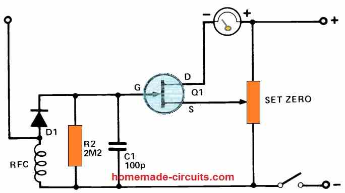 Because this FET is solely used as a DC amplifier, a 2N3819 or some other general-purpose transistor will suffice.
The "Set Zero" potentiometer can be anywhere between 1k and 10k.
When there is no RF signal present, the gate/source potential can be adjusted such that the meter only indicates a tiny current.
In the presence of an RF field this current slowly grows in proportion to the intensity of the RF signal, which is indicated on the meter.
A 100uA metre may be used for increasedsensitivity.
An ammeter with a lesser sensitivity, for examplelike250uA, 500uA, or 1mA, can also be utilized and mightprovide you with adequate information in most cases.
A VHF choke RFCcan be used if the field strength metre is exclusively usedwithVHF.
On the other hand,a short wave RFCchoke will be most appropriate for regular use with lower frequencies.
Because this FET is solely used as a DC amplifier, a 2N3819 or some other general-purpose transistor will suffice.
The "Set Zero" potentiometer can be anywhere between 1k and 10k.
When there is no RF signal present, the gate/source potential can be adjusted such that the meter only indicates a tiny current.
In the presence of an RF field this current slowly grows in proportion to the intensity of the RF signal, which is indicated on the meter.
A 100uA metre may be used for increasedsensitivity.
An ammeter with a lesser sensitivity, for examplelike250uA, 500uA, or 1mA, can also be utilized and mightprovide you with adequate information in most cases.
A VHF choke RFCcan be used if the field strength metre is exclusively usedwithVHF.
On the other hand,a short wave RFCchoke will be most appropriate for regular use with lower frequencies.
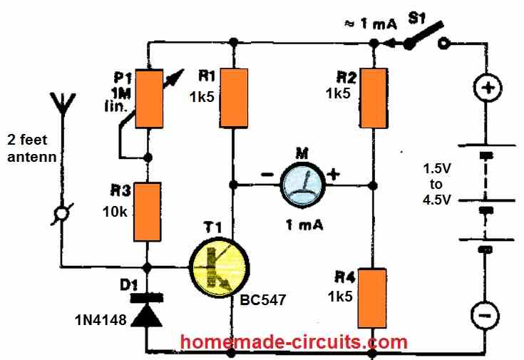 The antennawire which is a telescopic type antennais attached to the transistor's base.
As the HF voltage at the base of the antenna rises, the transistor is driven out of balance, causing the bridge to collapse.
The current subsequently passes via R2, the mA meter, and the transistor's collector-emitter junction, indicating the field strength on the meter.
Before turning on the transmitter for the testing, make sure thatthe meter needle us carefully adjusted tozero mark,using P1.
The antennawire which is a telescopic type antennais attached to the transistor's base.
As the HF voltage at the base of the antenna rises, the transistor is driven out of balance, causing the bridge to collapse.
The current subsequently passes via R2, the mA meter, and the transistor's collector-emitter junction, indicating the field strength on the meter.
Before turning on the transmitter for the testing, make sure thatthe meter needle us carefully adjusted tozero mark,using P1.
 However, using supplemental circuit stages connected to the output of the detector circuit, the device can be designed to switch on lamps, alarms, trigger a recording device, or maybe contact law enforcement.
Furthermore, the circuit could be designed to play a message whenever a person or an intruder is detected moving across its range of detection.
The circuit diagram for the Ultrasonic Motion Detector can be witnessed in the following figure.
However, using supplemental circuit stages connected to the output of the detector circuit, the device can be designed to switch on lamps, alarms, trigger a recording device, or maybe contact law enforcement.
Furthermore, the circuit could be designed to play a message whenever a person or an intruder is detected moving across its range of detection.
The circuit diagram for the Ultrasonic Motion Detector can be witnessed in the following figure.
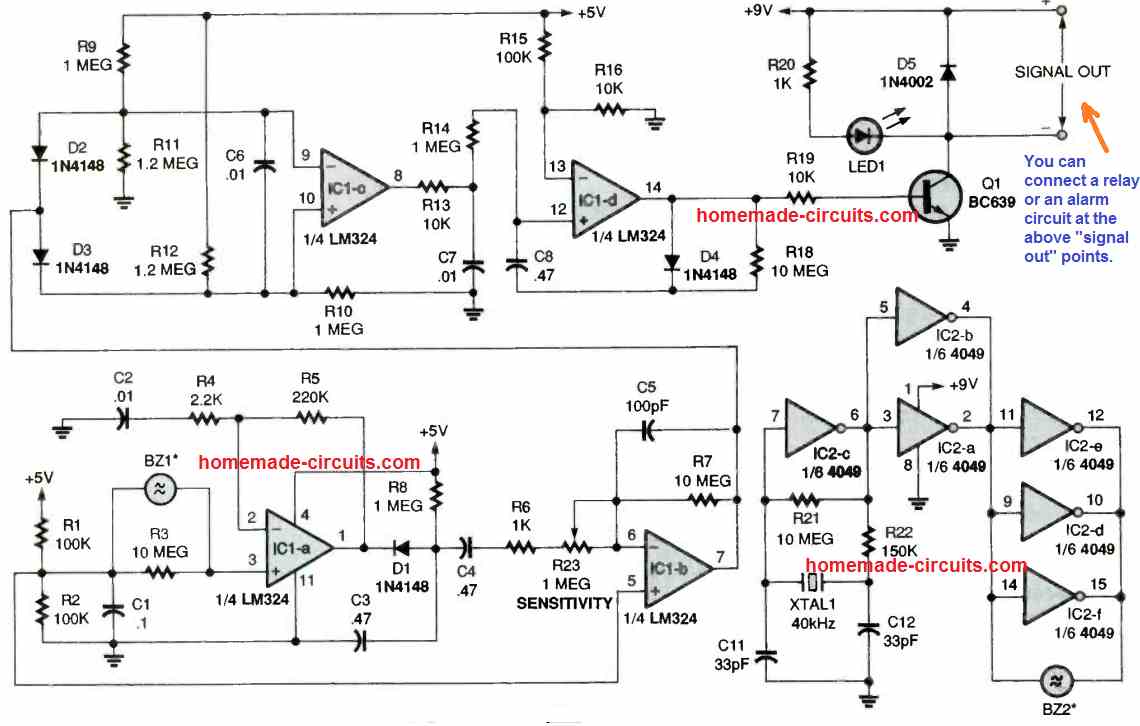 A 9 V PP3 battery, B1, instantly supplies electrical power for a few stages of the circuit.
The battery can be also seen attached with a 78L05 regulator, IC3, that supplies a 5 V DC supply to various other stages of the circuit.
A 9 V PP3 battery, B1, instantly supplies electrical power for a few stages of the circuit.
The battery can be also seen attached with a 78L05 regulator, IC3, that supplies a 5 V DC supply to various other stages of the circuit.
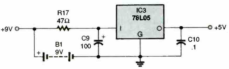

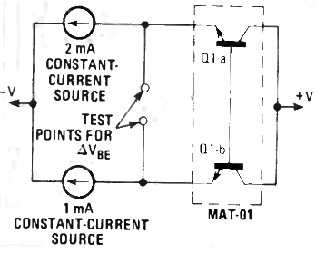 A differential opamp becomes necessary to enhance and increase the output voltage to some meaningful value.
It is advisable to calibrate the voltage range to 10 mV/ˇăK to ensure that an ordinary voltmeter could be employed.
To execute this with this BJT sensor, the differential opamp should possess a gain of over 167. When the output voltage reaches 10 mV/ˇăK, just about any 31/2 digit DVM could be taken to test the equivalent temperature across the transistor.
A differential opamp becomes necessary to enhance and increase the output voltage to some meaningful value.
It is advisable to calibrate the voltage range to 10 mV/ˇăK to ensure that an ordinary voltmeter could be employed.
To execute this with this BJT sensor, the differential opamp should possess a gain of over 167. When the output voltage reaches 10 mV/ˇăK, just about any 31/2 digit DVM could be taken to test the equivalent temperature across the transistor.
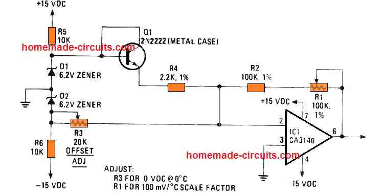 The transistor is used like a temperature sensor probe which must have a appropriate housing like a vintage voltmeter probe grip, a small section of metal tube, and so on.
In case the concept is implemented to determine the temperature within an existing device, it could be fitted entirely inside the unit and may not require an independent housing.
Nevertheless, no matter how it is positioned, a good thermal contact with the temperature that is being mesured is utmost crucial.
Two DC voltage references are used for this application +/-6.2 volts.
Diode D1 supplies the +6.2 V reference, while diode D2 delivers the -6.2 V reference.
The +6.2 supply is coupled to the collector/base pinout of the temperature sensor BJT (Q1).
Meaning, the emitter current of Q1 is going to be linearly incremental and sensitive only to temperature chnages since the collector voltage for Q1 is held constant.
This current is boosted by op amp IC1 to a level proportional to an output potential of 100 mV/ˇăK.
Variable resistor R1 can be adjusted for the calibration process to ensure the appropriate scaling level.
Again, any common 31/2 digit DVM may work nicely for reading the temperatures, although the display unit is going to be in degrees Kelvin.
If you want to change the measurement to degrees Celsius, you must be aware of the fact that the Kelvin and Celsius scales are identical, but offset by 273 degrees (0ˇă C = 273ˇă K).
To see temperature readings in degrees Celsius, an offset realignment will be required.
Potentiometer R3 switches the temperature range of the standard design from Kelvin to Celsius through summing of the countercurrent from the -6.2 V supply, using the current from the BJT.
The potentiometer is tweaked to generate zero output from amplifier IC1 with a sample temperature on the transistor set precisely 0ˇă C.
The transistor is used like a temperature sensor probe which must have a appropriate housing like a vintage voltmeter probe grip, a small section of metal tube, and so on.
In case the concept is implemented to determine the temperature within an existing device, it could be fitted entirely inside the unit and may not require an independent housing.
Nevertheless, no matter how it is positioned, a good thermal contact with the temperature that is being mesured is utmost crucial.
Two DC voltage references are used for this application +/-6.2 volts.
Diode D1 supplies the +6.2 V reference, while diode D2 delivers the -6.2 V reference.
The +6.2 supply is coupled to the collector/base pinout of the temperature sensor BJT (Q1).
Meaning, the emitter current of Q1 is going to be linearly incremental and sensitive only to temperature chnages since the collector voltage for Q1 is held constant.
This current is boosted by op amp IC1 to a level proportional to an output potential of 100 mV/ˇăK.
Variable resistor R1 can be adjusted for the calibration process to ensure the appropriate scaling level.
Again, any common 31/2 digit DVM may work nicely for reading the temperatures, although the display unit is going to be in degrees Kelvin.
If you want to change the measurement to degrees Celsius, you must be aware of the fact that the Kelvin and Celsius scales are identical, but offset by 273 degrees (0ˇă C = 273ˇă K).
To see temperature readings in degrees Celsius, an offset realignment will be required.
Potentiometer R3 switches the temperature range of the standard design from Kelvin to Celsius through summing of the countercurrent from the -6.2 V supply, using the current from the BJT.
The potentiometer is tweaked to generate zero output from amplifier IC1 with a sample temperature on the transistor set precisely 0ˇă C.
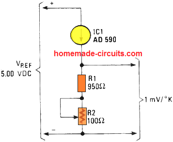 It maybe possible to use use the AD590 temperature sensor in many different ways.
One basic method is shown below, by connecting a series resistor of around 100 ohms.
This design is known as a 1-temperature, or 1-point, circuit.
The pot R2 can be tweaked to coincide the output voltage exactly in accordance with a standard mercury thermometer in some specified temperature.
Minor non-linear response in the device which is common in all semiconductor devices, might result in slight error at ranges far stripped away from the calibrated scale.
Another technique is to wire th¨¦ AD590 directly between a regulated +5 V reference source and the inverting input of an opamp.
It maybe possible to use use the AD590 temperature sensor in many different ways.
One basic method is shown below, by connecting a series resistor of around 100 ohms.
This design is known as a 1-temperature, or 1-point, circuit.
The pot R2 can be tweaked to coincide the output voltage exactly in accordance with a standard mercury thermometer in some specified temperature.
Minor non-linear response in the device which is common in all semiconductor devices, might result in slight error at ranges far stripped away from the calibrated scale.
Another technique is to wire th¨¦ AD590 directly between a regulated +5 V reference source and the inverting input of an opamp.
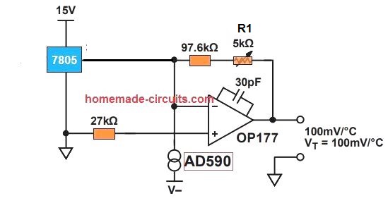 The range aspect of the sensor could be set up through a feedback resistor (RF) through the formula:
Vo = (I ¦ĚA/ˇăK) (RF) (T).
We could likewise use the AD590 with a double trim-point circuit employing an op amp as explained above.
The range aspect of the sensor could be set up through a feedback resistor (RF) through the formula:
Vo = (I ¦ĚA/ˇăK) (RF) (T).
We could likewise use the AD590 with a double trim-point circuit employing an op amp as explained above.
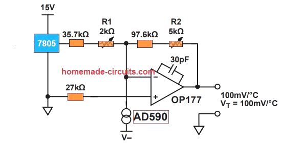 An offset current is summed up with the IC current at the inverting input of the op amp.
A couple of potentiometers could be wired up, one for controlling the offset and the other one for adjusting the gain, so that the circuit could be set up using two different temperatures, and thus minimizing the error.
An offset current is summed up with the IC current at the inverting input of the op amp.
A couple of potentiometers could be wired up, one for controlling the offset and the other one for adjusting the gain, so that the circuit could be set up using two different temperatures, and thus minimizing the error.
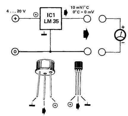 You can configure the LM35 sensor directly with an analogue or digital multimeter, or, more strangely enough, to a personal computer which could subsequently process and store the detected temperature data.
An appropriate software for this function can be searched online.
The reliability of the LM35/LM35C is normally 0.4 ˇăC at 25 ˇăC.
To make sure that the internal dissipation remains small, the load must be not lower than 5 k.
If an extended shielded cable is employed between the sensor and the meter, an RC configuration (a series 10 Ohm resistor with I ¦ĚF) must be attached between the output of the LM35 and the ground to protect against any kind of induced oscillations.
You can configure the LM35 sensor directly with an analogue or digital multimeter, or, more strangely enough, to a personal computer which could subsequently process and store the detected temperature data.
An appropriate software for this function can be searched online.
The reliability of the LM35/LM35C is normally 0.4 ˇăC at 25 ˇăC.
To make sure that the internal dissipation remains small, the load must be not lower than 5 k.
If an extended shielded cable is employed between the sensor and the meter, an RC configuration (a series 10 Ohm resistor with I ¦ĚF) must be attached between the output of the LM35 and the ground to protect against any kind of induced oscillations.
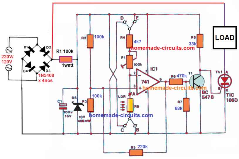 Referring to the schematic above, the working of this dual function light activated switch can be understood with the following points:
The op amp 741 forms the heart of the circuit and is wired as a comparator.
Its non-inverting input pin#3 is clamped with a fix reference derived from the junction of the resistive divider formed by R2/R3.
R2, R3 being equal in value, the reference voltage is set at the 50% of the zener voltage D5 which is used for stabilizing the rectified 310 VDC to 10 V DC.
The input DC power is supplied directly from the AC mains via a bridge rectifier set up, while the rectified DC high current is dropped through R1 to suit the attached electronic circuitry.
Now, the non-inverting pin of the op amp being fixed at around 5 V reference, the inverting input pin#2 is used for the detection of the light level via another resistive network formed by R1/P1 and the LDR.
Referring to the schematic above, the working of this dual function light activated switch can be understood with the following points:
The op amp 741 forms the heart of the circuit and is wired as a comparator.
Its non-inverting input pin#3 is clamped with a fix reference derived from the junction of the resistive divider formed by R2/R3.
R2, R3 being equal in value, the reference voltage is set at the 50% of the zener voltage D5 which is used for stabilizing the rectified 310 VDC to 10 V DC.
The input DC power is supplied directly from the AC mains via a bridge rectifier set up, while the rectified DC high current is dropped through R1 to suit the attached electronic circuitry.
Now, the non-inverting pin of the op amp being fixed at around 5 V reference, the inverting input pin#2 is used for the detection of the light level via another resistive network formed by R1/P1 and the LDR.
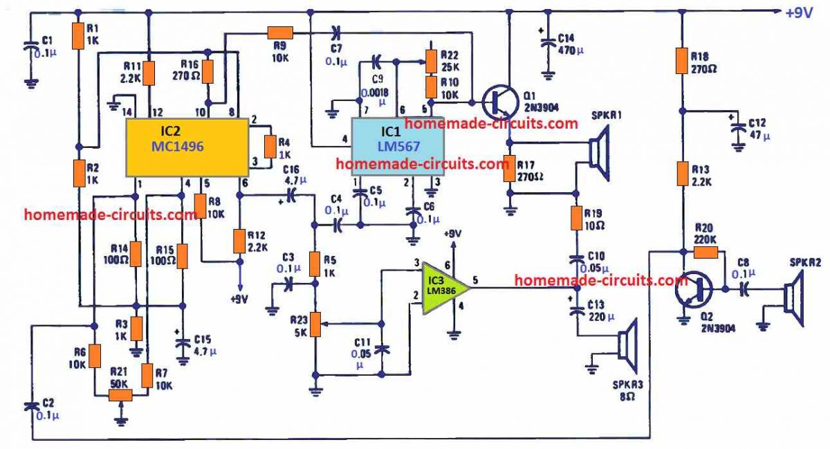 SPKR1 AND SPKR2 ARE 27 MM PIEZO TRANSDUCERS, SPKR3 CAN BE A SMALL 8¦¸ LOUDSPEAKER, HEADPHONE, OR AN AC VOLTMETER
Referring to the circuit diagram above, IC1 (a 567 phase-locked loop) is set up like a tunable oscillator having an output-frequency range of 15 to 25 kHz.
Potentiometer R22 is applied to adapt the output frequency of the oscillator.
The IC1 output is buffered by transistor Q1 and applied to transducer BZ1. The sound frequency reflected is captured by the second transducer BZ2, configured with the receiver stage of the circuit and applied to the base of Q2.
The boosted output through Q2 is applied to IC2 (which is connected like a double balanced mixer) at pin 1. One more sound signal (extracted from the output of IC1) is sent to IC2 at pin 10.
Resistor R21 (which is a 50k potentiometer) is employed like a carrier-balance control which is adjustable to ensure that the the oscillator's signal does not leak into the mixer output of chip IC2 at its pin 6.
The mixer's output at pin 6 of IC2 is applied via a low-pass filter on the Input of IC3 (which is built around the IC LM 386, low-voltage audio power amplifier).
A suitable loudspeaker or pair of headphones enables you to check the output from the IC3.
Potentiometer R23 is employed as a volume control.
SPKR1 AND SPKR2 ARE 27 MM PIEZO TRANSDUCERS, SPKR3 CAN BE A SMALL 8¦¸ LOUDSPEAKER, HEADPHONE, OR AN AC VOLTMETER
Referring to the circuit diagram above, IC1 (a 567 phase-locked loop) is set up like a tunable oscillator having an output-frequency range of 15 to 25 kHz.
Potentiometer R22 is applied to adapt the output frequency of the oscillator.
The IC1 output is buffered by transistor Q1 and applied to transducer BZ1. The sound frequency reflected is captured by the second transducer BZ2, configured with the receiver stage of the circuit and applied to the base of Q2.
The boosted output through Q2 is applied to IC2 (which is connected like a double balanced mixer) at pin 1. One more sound signal (extracted from the output of IC1) is sent to IC2 at pin 10.
Resistor R21 (which is a 50k potentiometer) is employed like a carrier-balance control which is adjustable to ensure that the the oscillator's signal does not leak into the mixer output of chip IC2 at its pin 6.
The mixer's output at pin 6 of IC2 is applied via a low-pass filter on the Input of IC3 (which is built around the IC LM 386, low-voltage audio power amplifier).
A suitable loudspeaker or pair of headphones enables you to check the output from the IC3.
Potentiometer R23 is employed as a volume control.
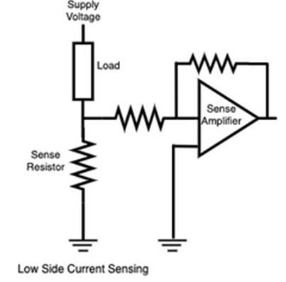
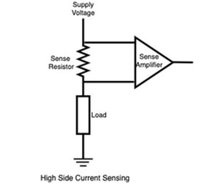 Low side sensing is easiest and inexpensive technique where you can connect a simple operational amplifier.
The current sensing circuit can be connected between the load and ground.
In discrete operational amplifiers (Op Amp) connecting the shunt with ground may introduce the noise, but this issue is resolved in NCS21xR.
While in high side current sensing, the monitor circuit should be connected between the supply and load.
The NCS21xR IC is very helpful for sensing current from both, high side and low side techniques.
The NCS21xR ICs series are high sensitivity current shunt monitors, which can be used for accurate current sensing applications.
Low side sensing is easiest and inexpensive technique where you can connect a simple operational amplifier.
The current sensing circuit can be connected between the load and ground.
In discrete operational amplifiers (Op Amp) connecting the shunt with ground may introduce the noise, but this issue is resolved in NCS21xR.
While in high side current sensing, the monitor circuit should be connected between the supply and load.
The NCS21xR IC is very helpful for sensing current from both, high side and low side techniques.
The NCS21xR ICs series are high sensitivity current shunt monitors, which can be used for accurate current sensing applications.
 IN- and IN+ pins are to be connected across the shunt resistor in the circuit.
Vs and GND pins are for power supply to the IC for operation.
OUT pin is designated for the output signal from the amplifier.
REF pin is to be connected with ground in unidirectional operation and in bidirectional operation REF should be connected with voltage reference circuit.
IN- and IN+ pins are to be connected across the shunt resistor in the circuit.
Vs and GND pins are for power supply to the IC for operation.
OUT pin is designated for the output signal from the amplifier.
REF pin is to be connected with ground in unidirectional operation and in bidirectional operation REF should be connected with voltage reference circuit.
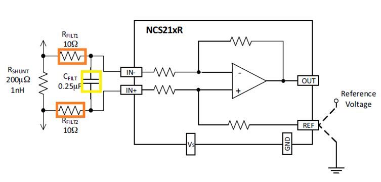 The wrong selection of filter resistor may lead to inaccurate gain.
It is recommended that the value of input resistor should less than or equal to 10¦¸.
A capacitor can be added to match the time constant of shunt resistor.
To filter a high frequency noise, the value of capacitor should be increased to a value that delivers the required filtering.
The wrong selection of filter resistor may lead to inaccurate gain.
It is recommended that the value of input resistor should less than or equal to 10¦¸.
A capacitor can be added to match the time constant of shunt resistor.
To filter a high frequency noise, the value of capacitor should be increased to a value that delivers the required filtering.
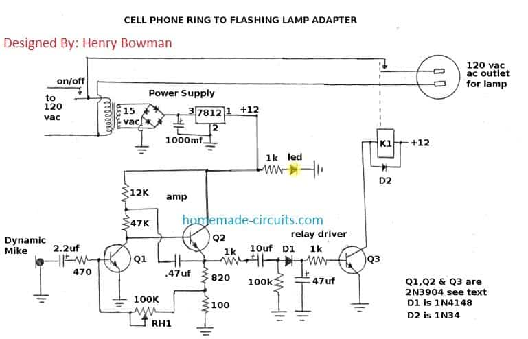

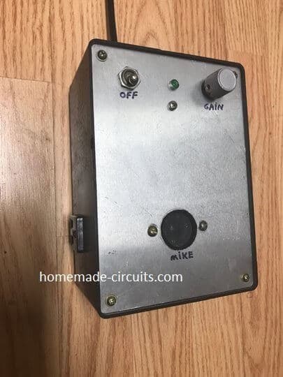
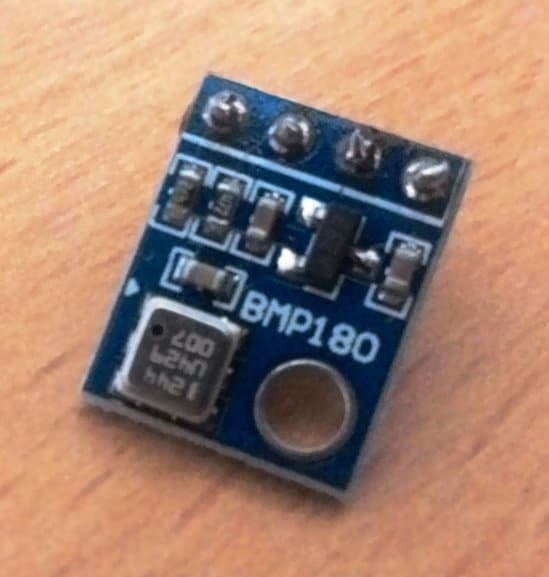
 Now, you know what a barometer is and where it is used.
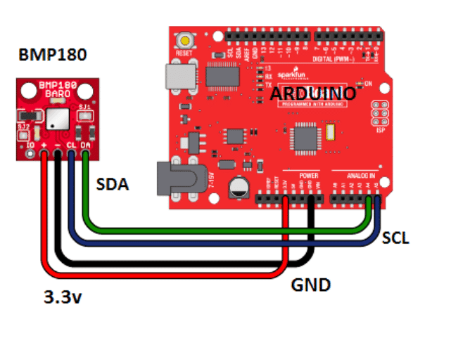 The barometric BMP180 sensorcircuit using Arduino is actually very simple as it utilizes i2C bus, which is two wire communication.
The chip uses 3.3V from Arduino from on-board regulated power supply.
It can measure local atmospheric pressure and ambient temperature.
The barometric BMP180 sensorcircuit using Arduino is actually very simple as it utilizes i2C bus, which is two wire communication.
The chip uses 3.3V from Arduino from on-board regulated power supply.
It can measure local atmospheric pressure and ambient temperature.
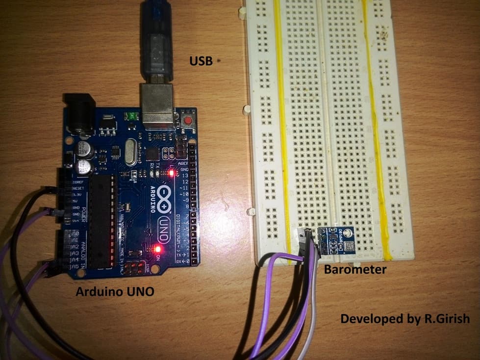 The program is designed to calculate other parameters too such as atmospheric pressure at sea level and altitude from sea level, which we can witness from Serial monitor of IDE.
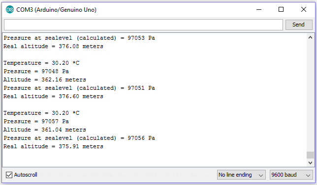 Before you dive into programming part, download the library file from the following link: github.com/adafruit/Adafruit_BMP085_Unified.git and add to Arduino library folder.
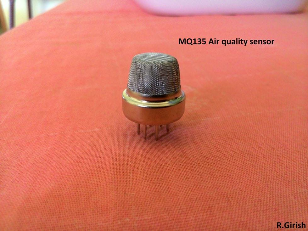 It is 6 terminal device which is symmetric in terminal placement; both the sides of the terminal are interchangeable.
Here is the illustration of pins:
It is 6 terminal device which is symmetric in terminal placement; both the sides of the terminal are interchangeable.
Here is the illustration of pins:
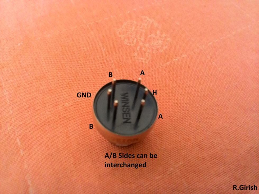 Here is a basic connection diagram:
 Two ˇ®AˇŻ pins are shorted internally and two ˇ®BˇŻ pins are shorted internally.
H and H pins is heater coil of the sensor.
The heater coil is used to heat up the air around the sensor, so that it can detect the chemical content in the air optimally.
The sensor can take up to few minutes to heat up to reach optimal working condition.
It not advisable to touch the sensor while operating because it can get pretty warm.
The sensor has an operating voltage of 5V; the sensor must be powered from external sources only, as it consumes about 200mA for heating.
The arduino voltage regulator canˇŻt deliver this much current.
For testing, you can connect a ammeter in mA range at the output pin B and bring a cigar gas lighter.
Try to leak the gas without igniting it near the sensor.
As the concentration of gas rises around the sensor, the current flow through ammeter increases.
If this works, your sensor is working normally.
Now, you know quite a bit about MQ-135 Sensor, letˇŻs move ahead and learn how to interface the MQ-135 with Arduino interfacing.
Two ˇ®AˇŻ pins are shorted internally and two ˇ®BˇŻ pins are shorted internally.
H and H pins is heater coil of the sensor.
The heater coil is used to heat up the air around the sensor, so that it can detect the chemical content in the air optimally.
The sensor can take up to few minutes to heat up to reach optimal working condition.
It not advisable to touch the sensor while operating because it can get pretty warm.
The sensor has an operating voltage of 5V; the sensor must be powered from external sources only, as it consumes about 200mA for heating.
The arduino voltage regulator canˇŻt deliver this much current.
For testing, you can connect a ammeter in mA range at the output pin B and bring a cigar gas lighter.
Try to leak the gas without igniting it near the sensor.
As the concentration of gas rises around the sensor, the current flow through ammeter increases.
If this works, your sensor is working normally.
Now, you know quite a bit about MQ-135 Sensor, letˇŻs move ahead and learn how to interface the MQ-135 with Arduino interfacing.
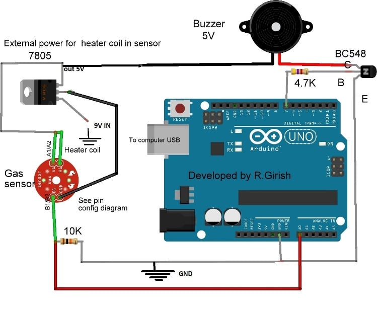 Make the connections as per the diagram, and check the gas sensor wire connection etc.
Rest of the circuit is self explanatory.
The analogue pin of Arduino measures the voltage from the gas sensor.
When the gas concentration rises above preset threshold in the program, the buzzer starts beeps.
The sensor takes a couple of minutes or so to warm up to reach optimal operating condition.
Until it reaches optimal working temperature, the values in the serial monitor fluctuates high and low.
It stabilizes after few minutes.
In the program the user can set the threshold value, it must be done only after careful observation on normal ambient concentration value in the serial monitor.
For instants, if the value fluctuates from 400 to 430, the threshold must set well above, like 500. It must not trigger the buzzer falsely.
The values displayed in the serial monitor are NOT ˇ®ppmˇŻ level of chemical concentration or anything like that.
It is mere measure of voltage level from the sensor; Arduino interprets the value from 0 to 1023. So we can say, higher the chemical concentration, higher the values get displayed.
Make the connections as per the diagram, and check the gas sensor wire connection etc.
Rest of the circuit is self explanatory.
The analogue pin of Arduino measures the voltage from the gas sensor.
When the gas concentration rises above preset threshold in the program, the buzzer starts beeps.
The sensor takes a couple of minutes or so to warm up to reach optimal operating condition.
Until it reaches optimal working temperature, the values in the serial monitor fluctuates high and low.
It stabilizes after few minutes.
In the program the user can set the threshold value, it must be done only after careful observation on normal ambient concentration value in the serial monitor.
For instants, if the value fluctuates from 400 to 430, the threshold must set well above, like 500. It must not trigger the buzzer falsely.
The values displayed in the serial monitor are NOT ˇ®ppmˇŻ level of chemical concentration or anything like that.
It is mere measure of voltage level from the sensor; Arduino interprets the value from 0 to 1023. So we can say, higher the chemical concentration, higher the values get displayed.
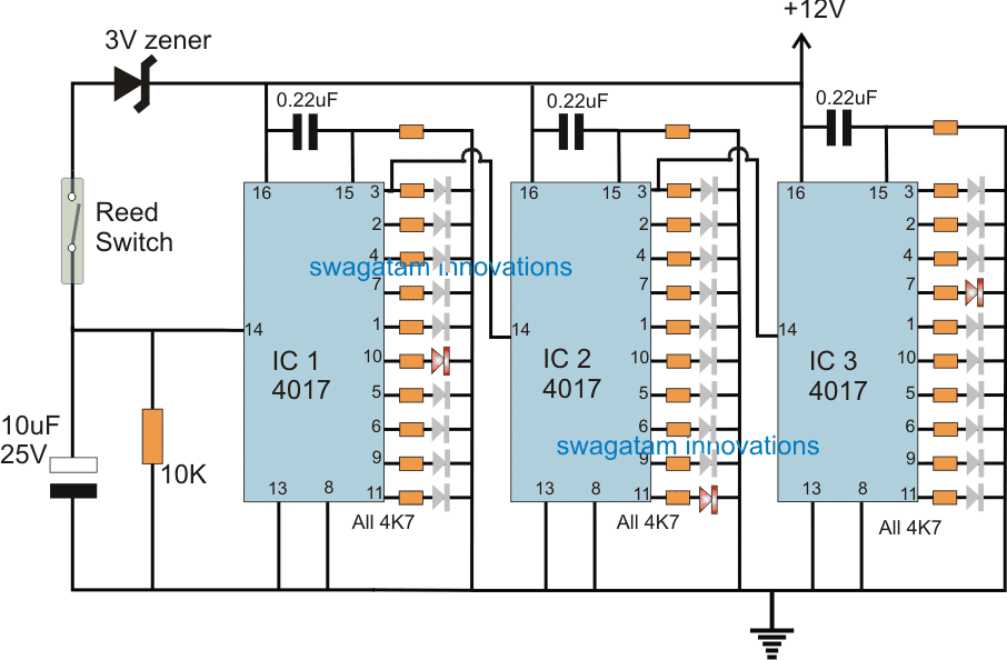 As can be seen in the above diagram, the reading for the winding count is simply achieved using LEDs across three IC 4017, this makes the assembly very straightforward and without any form special digital ICs or displays.
The idea is simple, the reed switch activates with every single rotation of the winding wheel which corresponds to a single turn count for the transformer winding.
This is indicated by the shifting or sequencing of the IC1 LED from its pin#3 to pin#11 constituting 10 winding count.
This implies IC1 LEDs jump from one pin to another in response to each rotation of the wheel which corresponds to one winding turn.
Identically IC2 LEDs sequence in response to every 10 winding count, and therefore each shifting of LED from one pin to another indicates 10 winding count.
The IC3 is also configured to implement a similar sequencing but it responds to every 10 winding count which means its LEDs jump from one pin to another in response to every 100 winding count or 100 numbers turn on the transformer.
In short, IC1 LEDs output sequencing completes one cycle with every 10 winding, IC2 with every 100 winding and IC3 with every 1000 winding.
Therefore the shown circuit has the limit of 1000 turn count, if more than this value is required then more IC stages could be added in the same manner as IC2 and IC3 are connected.
As can be seen in the above diagram, the reading for the winding count is simply achieved using LEDs across three IC 4017, this makes the assembly very straightforward and without any form special digital ICs or displays.
The idea is simple, the reed switch activates with every single rotation of the winding wheel which corresponds to a single turn count for the transformer winding.
This is indicated by the shifting or sequencing of the IC1 LED from its pin#3 to pin#11 constituting 10 winding count.
This implies IC1 LEDs jump from one pin to another in response to each rotation of the wheel which corresponds to one winding turn.
Identically IC2 LEDs sequence in response to every 10 winding count, and therefore each shifting of LED from one pin to another indicates 10 winding count.
The IC3 is also configured to implement a similar sequencing but it responds to every 10 winding count which means its LEDs jump from one pin to another in response to every 100 winding count or 100 numbers turn on the transformer.
In short, IC1 LEDs output sequencing completes one cycle with every 10 winding, IC2 with every 100 winding and IC3 with every 1000 winding.
Therefore the shown circuit has the limit of 1000 turn count, if more than this value is required then more IC stages could be added in the same manner as IC2 and IC3 are connected.
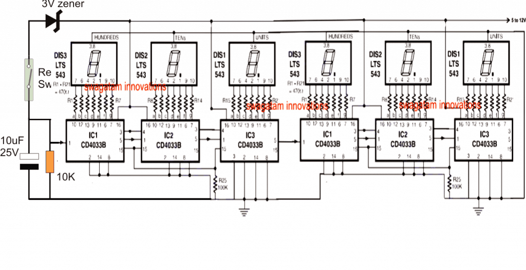 Here the reed switch and the associated parts remain identical to the previous LED version, and is rigged with the input of the 4033 counter module for the required triggering of the digits in response to each transformer winding count.

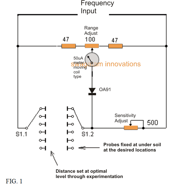 The proposed deep soil metal detector instrument includes the measuring bridge (figure 1), the alternating voltage generator (fig 2) and the a couple of probes, sunken inside the soil.
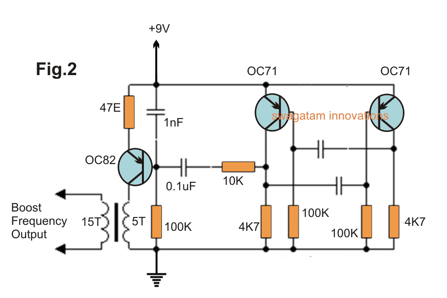 The resistances across the soil layers, between the electrodes of probes are coupled to the input of the bridge arms, for measuring the parameters.
Prior to measurement through 100 ohm resistor may be adjusted for bridging the balance so that the dial instrument readings are initially at the minimal.
The resistances across the soil layers, between the electrodes of probes are coupled to the input of the bridge arms, for measuring the parameters.
Prior to measurement through 100 ohm resistor may be adjusted for bridging the balance so that the dial instrument readings are initially at the minimal.
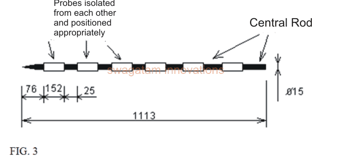 The design of the probe represented in FIG.3 may e understood as follows:
Each of the probes signifies the insulated rods having a diameter of around 1.5 mm.
on the surface area of the bar along its axle, these are fixed electrodes in the form of six thin-walled tube, separated from each other.
Each electrode probe with the aid of six cable connection is attached to the switch S1 measuring bridge, that in turn hooks up with one of the six pairs of electrodes together with the bridge.In this instance, each pair of electrodes at each of the positions of the switch S1 corresponds to the precise depth of the soil layer.
The design of the probe represented in FIG.3 may e understood as follows:
Each of the probes signifies the insulated rods having a diameter of around 1.5 mm.
on the surface area of the bar along its axle, these are fixed electrodes in the form of six thin-walled tube, separated from each other.
Each electrode probe with the aid of six cable connection is attached to the switch S1 measuring bridge, that in turn hooks up with one of the six pairs of electrodes together with the bridge.In this instance, each pair of electrodes at each of the positions of the switch S1 corresponds to the precise depth of the soil layer.
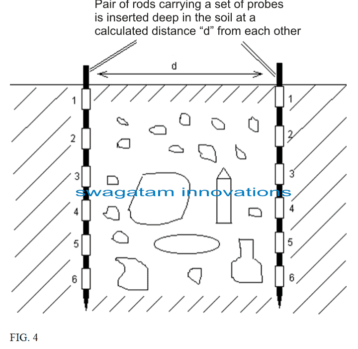 Soon after placing the probe on earth, in accordance with FIG.
4, the electrical resistance of the subsequent layers of soil located different depth is detected.
Evaluating the values acquired from the resistance, you are able to draw a conclusion at what depth (which soil layer) are objects that might be changing the resistance of the soil.
The space between the probes are pretty much decided on in each specific scenario.
Occasionally, great outcomes could be obtained with distance that me approximately close to 2.4 m.
The variable resistor of the bridge is 500 ohms as shown in the deep soil metal detector circuit diagram, is for controlling the sensitivity of the bridge depending on soil type being investigated.
Courtesy: The Radio-Constructor, 1966, 8
Soon after placing the probe on earth, in accordance with FIG.
4, the electrical resistance of the subsequent layers of soil located different depth is detected.
Evaluating the values acquired from the resistance, you are able to draw a conclusion at what depth (which soil layer) are objects that might be changing the resistance of the soil.
The space between the probes are pretty much decided on in each specific scenario.
Occasionally, great outcomes could be obtained with distance that me approximately close to 2.4 m.
The variable resistor of the bridge is 500 ohms as shown in the deep soil metal detector circuit diagram, is for controlling the sensitivity of the bridge depending on soil type being investigated.
Courtesy: The Radio-Constructor, 1966, 8
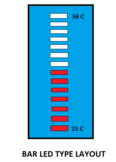 The above illustrated layout may be adopted for best looking for your setup.
The user just needs to enter the minimum temperature range of the room.
It can be a rough value, which can be later changed once full hardware setup is completed.
If the temperature range goes below the threshold value that user entered, no LED will glow and if the temperature goes beyond the maximum range (minimum + 11) all LED would glow.
If there are any sensor connectivity issues, all the LED will blink every second simultaneously.
The above illustrated layout may be adopted for best looking for your setup.
The user just needs to enter the minimum temperature range of the room.
It can be a rough value, which can be later changed once full hardware setup is completed.
If the temperature range goes below the threshold value that user entered, no LED will glow and if the temperature goes beyond the maximum range (minimum + 11) all LED would glow.
If there are any sensor connectivity issues, all the LED will blink every second simultaneously.
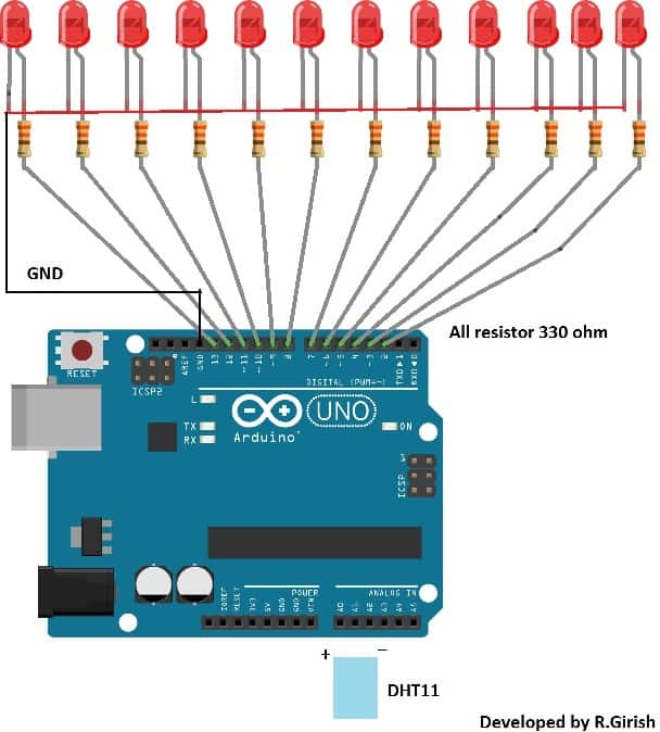 Thus, your LED thermometer circuit setup is complete and ready to upload the code.
It is always recommended to test the circuit on bread board before making it permanent.
Tip: Use different color LED for indicating different temperature ranges.
You may use blue LEDs for lower temperature range, green or yellow for mid temperature range and red LEDs for higher temperature.
This will make more attractive.
Thus, your LED thermometer circuit setup is complete and ready to upload the code.
It is always recommended to test the circuit on bread board before making it permanent.
Tip: Use different color LED for indicating different temperature ranges.
You may use blue LEDs for lower temperature range, green or yellow for mid temperature range and red LEDs for higher temperature.
This will make more attractive.
 NOTE: The following program is only compatible with DHT11 sensor.
Before proceeding, please make sure to download the library file form the following link:
https://arduino-info.wikispaces.com/file/detail/DHT-lib.zip
NOTE: The following program is only compatible with DHT11 sensor.
Before proceeding, please make sure to download the library file form the following link:
https://arduino-info.wikispaces.com/file/detail/DHT-lib.zip
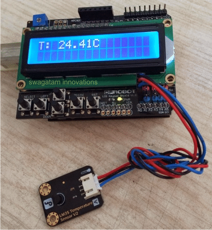 There's actually nothing too much explainable in this configuration, since everything is module based and simply requires hooking up or plugging-in with each other through the offered male female sockets and connectors.
 2) A Compatible LCD Module
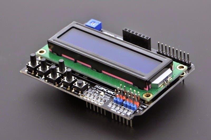 3) An analogue temperature sensor chip, such as a DS18B20 or our very own LM35 IC.
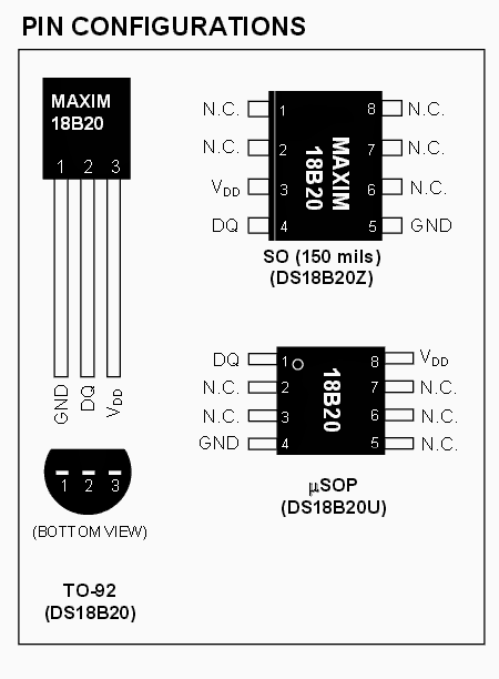 4) A 9V, 1 amp AC to DC adapter unit
Now it's just about pushing in the connectors with each other, do a bit of setting through the LCD push buttons, and you get a full fledged, accurate digital LCD temperature meter at your disposal.
You can measure room temperature with this set up, or clamp the sensor appropriately with any heat emitting device which needs to be monitored such as an automobile engine, egg incubator chamber, geyser, or simply to check the heat dissipation from a power amplifier devices.
4) A 9V, 1 amp AC to DC adapter unit
Now it's just about pushing in the connectors with each other, do a bit of setting through the LCD push buttons, and you get a full fledged, accurate digital LCD temperature meter at your disposal.
You can measure room temperature with this set up, or clamp the sensor appropriately with any heat emitting device which needs to be monitored such as an automobile engine, egg incubator chamber, geyser, or simply to check the heat dissipation from a power amplifier devices.
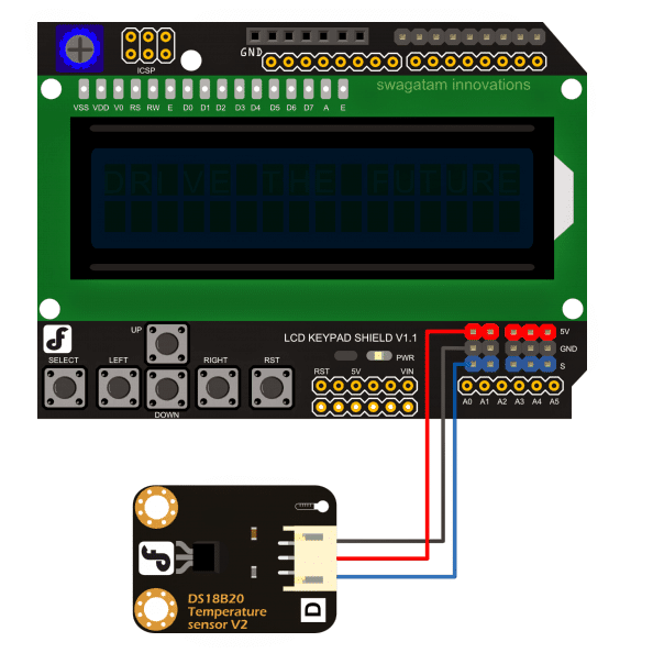 But before you implement the above set up, you'll need to program the Arduino board with the following sample code.
OneWire ourWire(DS18B20);
DallasTemperature sensor(&ourWire);
LiquidCrystal lcd(7, 6, 5, 4, 3, 2);
byte degree_symbol[8] =
{
0b00111,
0b00101,
0b00111,
0b00000,
0b00000,
0b00000,
0b00000,
0b00000
};
void setup()
{
Serial.begin(9600);
delay(1000);
sensor.begin();
lcd.begin(16, 2);
lcd.createChar(1, degree_symbol);
lcd.clear();
lcd.setCursor(0,0);
lcd.print("Temp: ");
}
void loop()
{
sensor.requestTemperatures();
Serial.print(sensor.getTempCByIndex(0));
Serial.println("ˇăC");
lcd.setCursor(7,0);
lcd.print(sensor.getTempCByIndex(0));
lcd.write(1);
lcd.print("C");
delay(1000);
}
Courtesy: dfrobot.com/wiki/index.php?title=LCD_KeyPad_Shield_For_Arduino_SKU:_DFR0009
But before you implement the above set up, you'll need to program the Arduino board with the following sample code.
OneWire ourWire(DS18B20);
DallasTemperature sensor(&ourWire);
LiquidCrystal lcd(7, 6, 5, 4, 3, 2);
byte degree_symbol[8] =
{
0b00111,
0b00101,
0b00111,
0b00000,
0b00000,
0b00000,
0b00000,
0b00000
};
void setup()
{
Serial.begin(9600);
delay(1000);
sensor.begin();
lcd.begin(16, 2);
lcd.createChar(1, degree_symbol);
lcd.clear();
lcd.setCursor(0,0);
lcd.print("Temp: ");
}
void loop()
{
sensor.requestTemperatures();
Serial.print(sensor.getTempCByIndex(0));
Serial.println("ˇăC");
lcd.setCursor(7,0);
lcd.print(sensor.getTempCByIndex(0));
lcd.write(1);
lcd.print("C");
delay(1000);
}
Courtesy: dfrobot.com/wiki/index.php?title=LCD_KeyPad_Shield_For_Arduino_SKU:_DFR0009
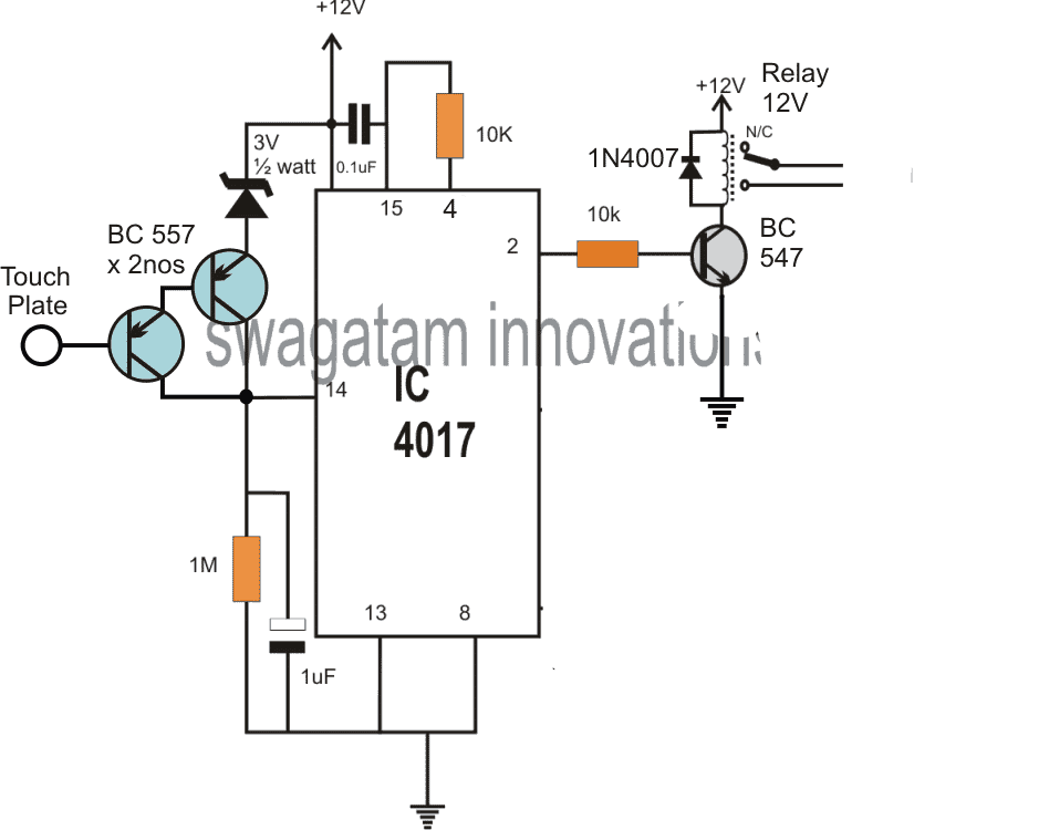 The IC basically consists of 10 outputs, starting from its pin#3 and randomly ending at pin#11, constituting 10 outputs which are designed to produce a sequencing or shifting high logics across these output pins in response to every single positive pulse applied at its pin#14.
The sequencing does not need to finish at the last pin#11, rather could be assigned to stop at any desired intermediate pinout, and revert to the first pin#3 to initiate the cycle afresh.
This is simply done by connecting the end sequence pinout with the reset pin#15 of the IC.
This makes sure that whenever the sequence reaches this pinout, the cycle stops here and reverts to pin#3 which is the initial pinout for enabling a repeat cycling of the sequence in the same order.
For example in our design pin#4 which is the third pinout in the sequence can be seen attached to pin#15 of the IC, implies that as the sequence jumps from pin#3 to the next pin#2, and then to pin#4 it instantly reverts or flips back to pin#3 to enable the cycle again.
The IC basically consists of 10 outputs, starting from its pin#3 and randomly ending at pin#11, constituting 10 outputs which are designed to produce a sequencing or shifting high logics across these output pins in response to every single positive pulse applied at its pin#14.
The sequencing does not need to finish at the last pin#11, rather could be assigned to stop at any desired intermediate pinout, and revert to the first pin#3 to initiate the cycle afresh.
This is simply done by connecting the end sequence pinout with the reset pin#15 of the IC.
This makes sure that whenever the sequence reaches this pinout, the cycle stops here and reverts to pin#3 which is the initial pinout for enabling a repeat cycling of the sequence in the same order.
For example in our design pin#4 which is the third pinout in the sequence can be seen attached to pin#15 of the IC, implies that as the sequence jumps from pin#3 to the next pin#2, and then to pin#4 it instantly reverts or flips back to pin#3 to enable the cycle again.
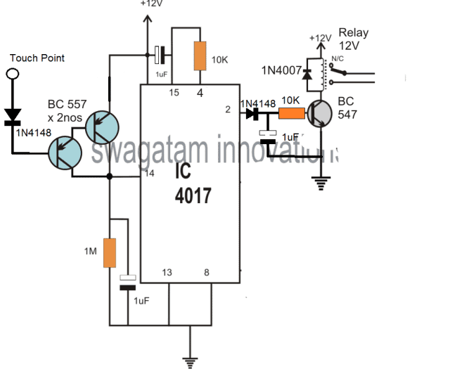 Or you may also follow the diagram which is shown in the video.
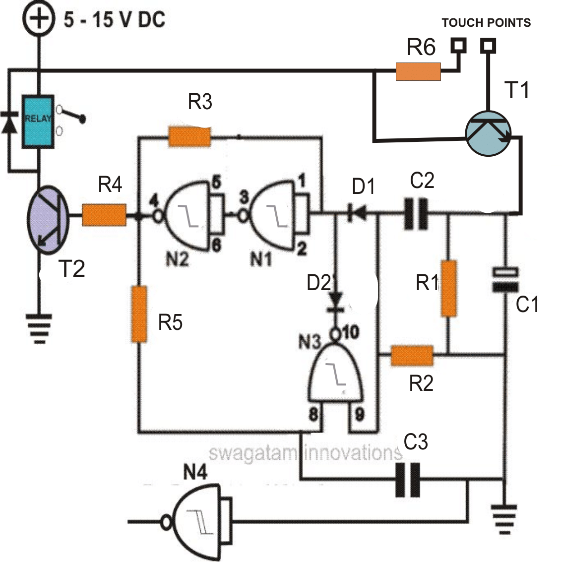
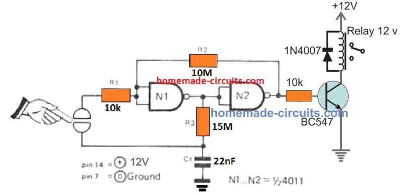
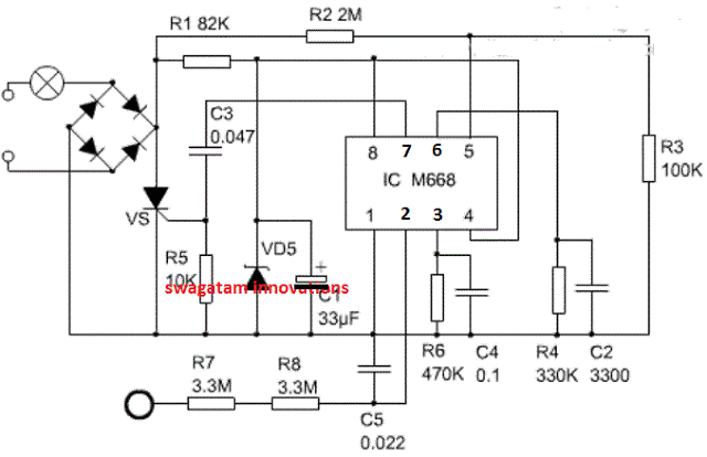 The touch plate is connected with a current limiting network using R7/R8 so that no shock sensation is felt by the user while putting finger on this touch pad.
The various pinout functions of the IC can be learned from the following points:
The supply positive is applied to pin#8 and ground to pin#1 (negative) The touch signal on the touch pad is sent to pin#2, and the logic is transformed into an ON or OFF at the output pin#7.
This signal from pin#7 subsequently drives the SCR and the connected load into either ON or OFF states.
C3 makes sure that the SCR is not false triggered due to multiple pulses in response to an improper or inadequate touching on the touch pad.
R4 and C2 forms an oscillator stage for enabling the required processing of the signals within the IC.
A synchronization signal from R2/R5 is divided internal through pin#5 of the IC.
Pin#4 of the IC has a very crucial and interesting function.
When connected with the positive line or Vcc, the IC enables the output to alternately toggle ON/OFF, allowing the light or the load to switch ON and OFF alternately in response to every touch on the touch pad.
However when pin#4 isconnected to the ground or the negative line Vss, it transforms the IC into a 4 stage dimmer circuit.
Meaning in this position every touch on the touch pad causes the load ( a lamp for example) to reduce or increase its intensity sequentially, in a gradually dimming or gradually brightening manner ( and OFF at the ends).
If you have any questions regarding the functioning of the above discussed mains touch switch circuit please write them down through the comment box...
The touch plate is connected with a current limiting network using R7/R8 so that no shock sensation is felt by the user while putting finger on this touch pad.
The various pinout functions of the IC can be learned from the following points:
The supply positive is applied to pin#8 and ground to pin#1 (negative) The touch signal on the touch pad is sent to pin#2, and the logic is transformed into an ON or OFF at the output pin#7.
This signal from pin#7 subsequently drives the SCR and the connected load into either ON or OFF states.
C3 makes sure that the SCR is not false triggered due to multiple pulses in response to an improper or inadequate touching on the touch pad.
R4 and C2 forms an oscillator stage for enabling the required processing of the signals within the IC.
A synchronization signal from R2/R5 is divided internal through pin#5 of the IC.
Pin#4 of the IC has a very crucial and interesting function.
When connected with the positive line or Vcc, the IC enables the output to alternately toggle ON/OFF, allowing the light or the load to switch ON and OFF alternately in response to every touch on the touch pad.
However when pin#4 isconnected to the ground or the negative line Vss, it transforms the IC into a 4 stage dimmer circuit.
Meaning in this position every touch on the touch pad causes the load ( a lamp for example) to reduce or increase its intensity sequentially, in a gradually dimming or gradually brightening manner ( and OFF at the ends).
If you have any questions regarding the functioning of the above discussed mains touch switch circuit please write them down through the comment box...
 Referring to the circuit above, the four diodes at the input form the basic bridge rectifier circuit for rectifying the mains AC into DC.
This rectified DC is stabilized by the 12V zener and filtered by C2 to acquire a fairly clean DC for the accompanying touch switch circuit.
R5 is used for limiting the input mains current to a much lower level suitable for operating the circuit safely.
An LED can be seen connected with this supply which ensures a dim light is always ON near the circuit for facilitating quick location of the touch switch pad.
The IC used in this transformers touch lamp with delay circuit is a double D flip-flip IC 4013, which has 2 flip flop stages built inside it, here we make use of one of these stages for our application.
Whenever the indicated touch pad is touched by finger, our body offers a leakage current on the point causing a momentary high logic on pin#3 of the IC, which in turn causes the pin#1 of the IC to go high.
When this happen the attached triac is triggered via R4, and the bridge rectifier completes its cycle powering the series lamp.
The lamp now illuminates brightly.
Also in the meantime, the capacitor C1 gradually starts charging via R3, and when it gets fully charged pin#4 is rendered with a high logic which resets the flip flop in its original condition.
This instantly turns pin#1 low switching OFF the SCR and the lamp.
The value of the R3/C1 produces a delay of about 1 minute, this can be increased or decreased by suitably increasing or decreasing the values of these two RC components as per individual preference.
Referring to the circuit above, the four diodes at the input form the basic bridge rectifier circuit for rectifying the mains AC into DC.
This rectified DC is stabilized by the 12V zener and filtered by C2 to acquire a fairly clean DC for the accompanying touch switch circuit.
R5 is used for limiting the input mains current to a much lower level suitable for operating the circuit safely.
An LED can be seen connected with this supply which ensures a dim light is always ON near the circuit for facilitating quick location of the touch switch pad.
The IC used in this transformers touch lamp with delay circuit is a double D flip-flip IC 4013, which has 2 flip flop stages built inside it, here we make use of one of these stages for our application.
Whenever the indicated touch pad is touched by finger, our body offers a leakage current on the point causing a momentary high logic on pin#3 of the IC, which in turn causes the pin#1 of the IC to go high.
When this happen the attached triac is triggered via R4, and the bridge rectifier completes its cycle powering the series lamp.
The lamp now illuminates brightly.
Also in the meantime, the capacitor C1 gradually starts charging via R3, and when it gets fully charged pin#4 is rendered with a high logic which resets the flip flop in its original condition.
This instantly turns pin#1 low switching OFF the SCR and the lamp.
The value of the R3/C1 produces a delay of about 1 minute, this can be increased or decreased by suitably increasing or decreasing the values of these two RC components as per individual preference.
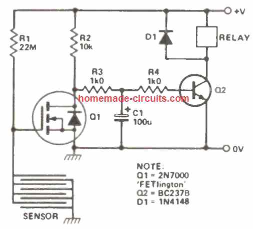 As soon as the sensor plate is touched, it instantly causes a grounding of the R1 voltage through the finger, forcing the MOSFET to turn OFF.
When the MOSFET is turned OFF, the Q2 transistor gets the access to the potential from the R2, and it turns ON now, When Q2 turns ON, the relay coil gets the required amount of power, and it also turns ON, switching ON any load that may have been configured across its contacts.
Removing the finger from the touch sensor, restores the circuit to its original form, and the relay switches OFF.
As soon as the sensor plate is touched, it instantly causes a grounding of the R1 voltage through the finger, forcing the MOSFET to turn OFF.
When the MOSFET is turned OFF, the Q2 transistor gets the access to the potential from the R2, and it turns ON now, When Q2 turns ON, the relay coil gets the required amount of power, and it also turns ON, switching ON any load that may have been configured across its contacts.
Removing the finger from the touch sensor, restores the circuit to its original form, and the relay switches OFF.
 The complete working of the above 4049 based circuit can be studies through the following instructions


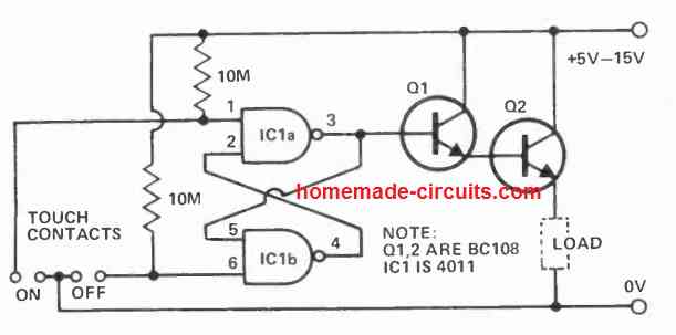 When the 'on' contacts are touched with a finger causes pin 3 to become high, which turns on the darlington pair and power is supplied to the load.
When the 'off' contacts are touched, the opposite happens, and the action switches OFF the load.
Q1 needs to be a high gain transistor, and Q2 picked out according to the current specifications of the load.
When the 'on' contacts are touched with a finger causes pin 3 to become high, which turns on the darlington pair and power is supplied to the load.
When the 'off' contacts are touched, the opposite happens, and the action switches OFF the load.
Q1 needs to be a high gain transistor, and Q2 picked out according to the current specifications of the load.
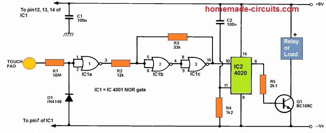 Because the IC 4001circuit's input impedance is so large, the backward resistance of D1 is utilized to connect the input to ground during idle situations, preventing erroneous activity.
In combination with the circuit's input capacitance, R1 works as a low pass filter, attenuating noise and interference that may be encountered on the 50Hz mains signal.
The output from gate 1 still has substantial amount ofnoise components and a rise time that is insufficient to operate the circuit's end stage.
The trigger circuit built around gates 2 and 3 is used to resolve this issue.
Due to the connection with R2, R3 tries to keep gate 2 input in almost the same condition as gate 3 output, preventing any change in logic state induced by gate 1 output.
Because R2 is smaller than R3, gate 1 can drivethe trigger circuit if its output signal is large enough.
The main 50Hz signal will be powerful indeed, however the noise spikes may not, and therefore will be removed from the trigger's output.
The connection across R3 guarantees a fast shift whenever the trigger's output beginschangingstate.IC2 is a 14-stage binary (division by 2) counter, and Q1 is operatedfrom the output of the seventh stage via current limit resistor R5. At power up, C2 and R4 send a positive reset pulse to the counter, causing the outputs to be low and Q1 to be turned off.
The load for transistorQ1 is formed by the regulated device, which apparently gets no substantial power.
A 50Hz signal is provided to IC2 when the touch contact is activated, and the 7th stage output swapsstate after 64 pulses.
The load is turned on and off as this output swings high and low.
In practice, the contact is held just long enough for the unit to transition to the ideal state (which the userwantsto do automatically).
In the "off" position, the unit uses around 1uA, while in the "on" position, it draws roughly 3mA.
Because the IC 4001circuit's input impedance is so large, the backward resistance of D1 is utilized to connect the input to ground during idle situations, preventing erroneous activity.
In combination with the circuit's input capacitance, R1 works as a low pass filter, attenuating noise and interference that may be encountered on the 50Hz mains signal.
The output from gate 1 still has substantial amount ofnoise components and a rise time that is insufficient to operate the circuit's end stage.
The trigger circuit built around gates 2 and 3 is used to resolve this issue.
Due to the connection with R2, R3 tries to keep gate 2 input in almost the same condition as gate 3 output, preventing any change in logic state induced by gate 1 output.
Because R2 is smaller than R3, gate 1 can drivethe trigger circuit if its output signal is large enough.
The main 50Hz signal will be powerful indeed, however the noise spikes may not, and therefore will be removed from the trigger's output.
The connection across R3 guarantees a fast shift whenever the trigger's output beginschangingstate.IC2 is a 14-stage binary (division by 2) counter, and Q1 is operatedfrom the output of the seventh stage via current limit resistor R5. At power up, C2 and R4 send a positive reset pulse to the counter, causing the outputs to be low and Q1 to be turned off.
The load for transistorQ1 is formed by the regulated device, which apparently gets no substantial power.
A 50Hz signal is provided to IC2 when the touch contact is activated, and the 7th stage output swapsstate after 64 pulses.
The load is turned on and off as this output swings high and low.
In practice, the contact is held just long enough for the unit to transition to the ideal state (which the userwantsto do automatically).
In the "off" position, the unit uses around 1uA, while in the "on" position, it draws roughly 3mA.
 The data pin always should be connected with a pull-up resistor from 4.7K to 10K.
The above illustrated sensor came with PCB with eliminated NC pin and with pull-up resistor.
But some sensors come without those feature, without the pull-up resistor the readings send to arduino will be fatally error values.
Now we are going to interface DHT sensor with arduino.
Before proceeding the project download the library file form the following link:
https://arduino-info.wikispaces.com/file/detail/DHT-lib.zip
You just need these four components: DHTxx sensor, arduino Uno, USB cable, and a PC.
Just insert the sensor on analog pins of the arduino as illustrated in prototype and dump the code to arduino, open the serial monitor and you can see the readings.
AuthorˇŻs prototype:
The data pin always should be connected with a pull-up resistor from 4.7K to 10K.
The above illustrated sensor came with PCB with eliminated NC pin and with pull-up resistor.
But some sensors come without those feature, without the pull-up resistor the readings send to arduino will be fatally error values.
Now we are going to interface DHT sensor with arduino.
Before proceeding the project download the library file form the following link:
https://arduino-info.wikispaces.com/file/detail/DHT-lib.zip
You just need these four components: DHTxx sensor, arduino Uno, USB cable, and a PC.
Just insert the sensor on analog pins of the arduino as illustrated in prototype and dump the code to arduino, open the serial monitor and you can see the readings.
AuthorˇŻs prototype:


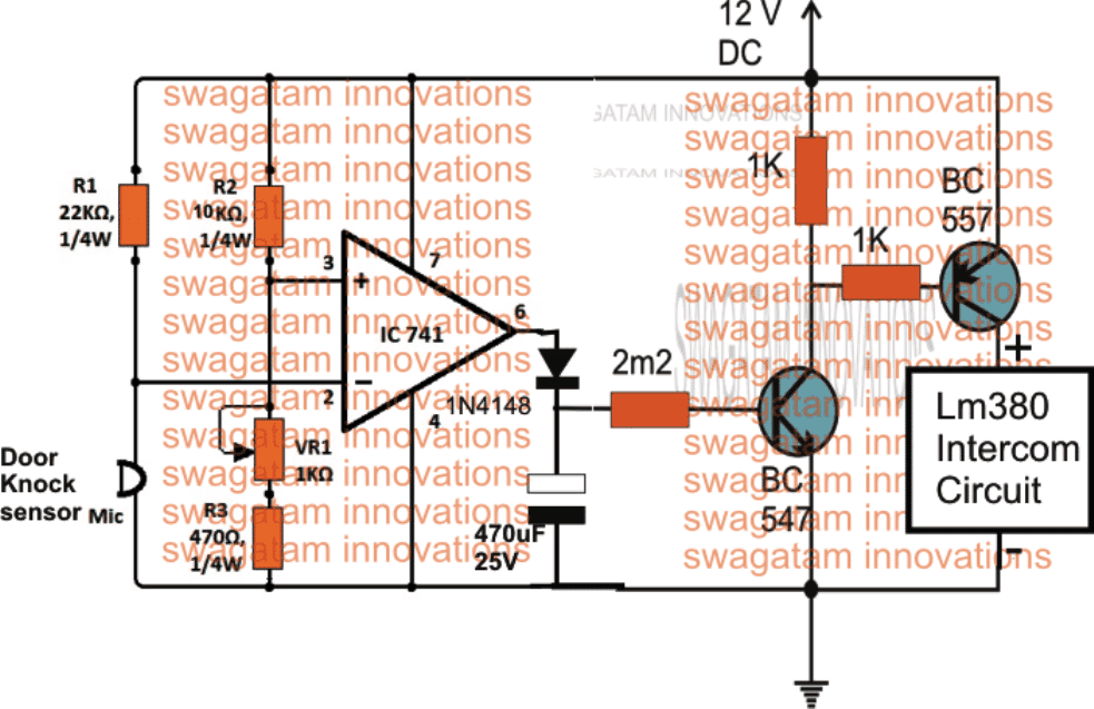
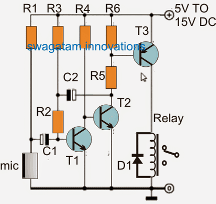
 In the discussed sound triggered remote control circuit, a MiC is configured across pin3 of the IC.
An external matching frequency (2kHz) in the form of an audible sound or whistle is pointed toward the mic such that the sound hits the mic starighton.
The mic converts the sound into electrical pulses corresponding to the received frequency at the relevant input pin of the IC.
The IC immediately acknowledges the matching data and reverts the output into a low for the necessary actions.
The output may be directly connected with a relay if only a momentary toggling is required or only for the time the input is active.
For an ON/OFF switching the same may be configured with a FLIP-FLOP circuit.
In the discussed sound triggered remote control circuit, a MiC is configured across pin3 of the IC.
An external matching frequency (2kHz) in the form of an audible sound or whistle is pointed toward the mic such that the sound hits the mic starighton.
The mic converts the sound into electrical pulses corresponding to the received frequency at the relevant input pin of the IC.
The IC immediately acknowledges the matching data and reverts the output into a low for the necessary actions.
The output may be directly connected with a relay if only a momentary toggling is required or only for the time the input is active.
For an ON/OFF switching the same may be configured with a FLIP-FLOP circuit.
 For the sensor, a 27mm piezo transducer will work the best, the following figure shows the image of this device:
 So, if any bolt or both bolt are used from inside, it complete the circuit and LED will glow.
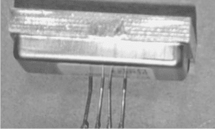
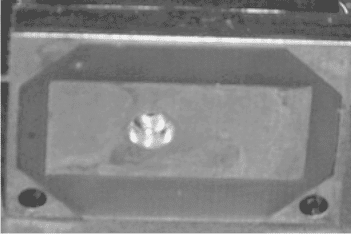 Once this reflected frequency shift is detected by the sensor, the in built circuitry instantly mixes the reflected frequency with the existing original frequency and produces two individual frequencies across its specified outputs.
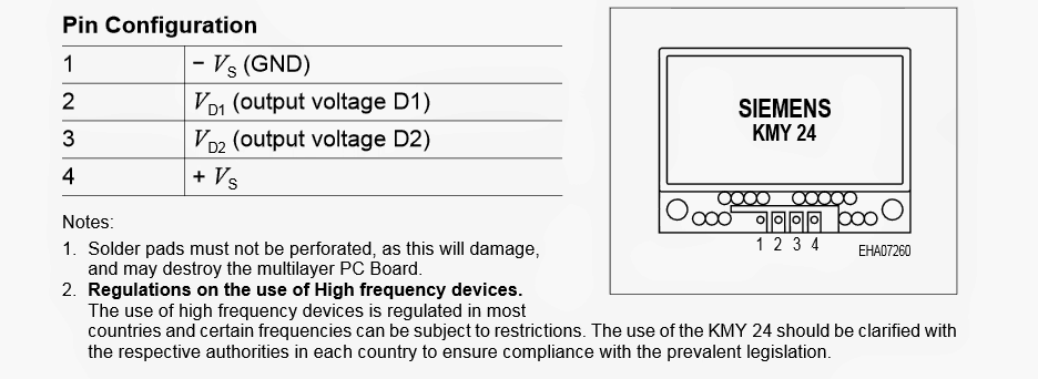 The next image provides the breakdown parameters or the absolute maximum voltage and current ratings that must be applied to the IC, these parameters must not be exceeded, to be precise these must be kept well below the shown values.
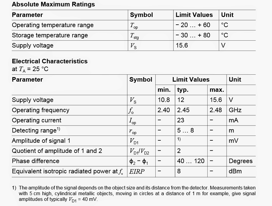 The two images shown below depict the phase shift or the difference in the position of the reflected frequency relative to the original radiated frequency when the target is approaching (first image below), and when the target is receding or going back (the second diagram below).
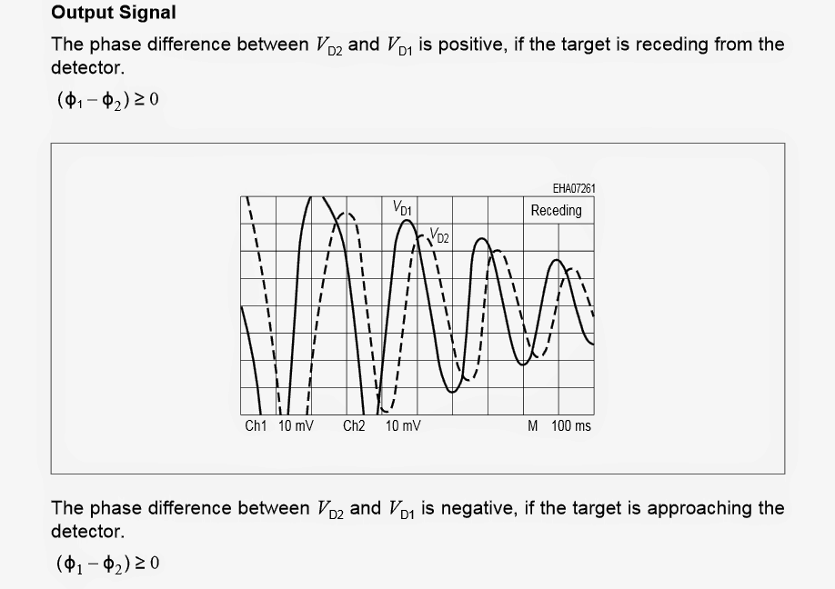
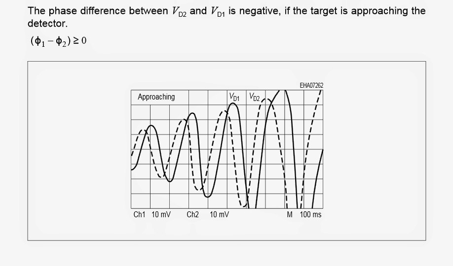 In the next (upcoming) article we'll try to understand regarding how to use a microwave sensor through a practical circuit.
 I've listened to sound recordings like whistlers etc and not one of these sounds matches the recordings I've collected from what I've received on my gravity wave detectors,
 Parts ListR1 = 2M2,R2 = 100K,R3 = 1K, C1 = 0.01uF, A1, A2 = IC 324
Referring to the above simple thunder lightning detector circuit, the configuration is basically a couple of opamps from the IC LM324 wired up as a high gain amplifier circuit.
Parts ListR1 = 2M2,R2 = 100K,R3 = 1K, C1 = 0.01uF, A1, A2 = IC 324
Referring to the above simple thunder lightning detector circuit, the configuration is basically a couple of opamps from the IC LM324 wired up as a high gain amplifier circuit.


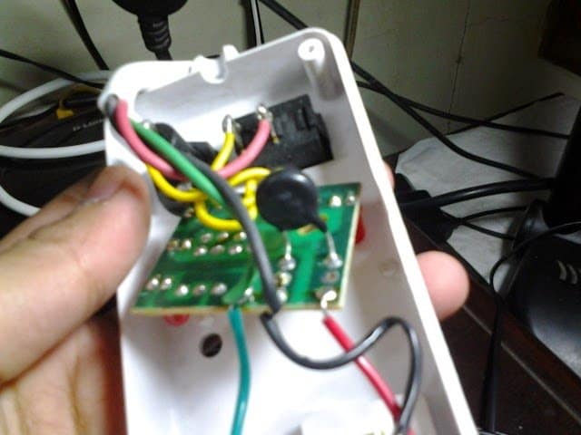
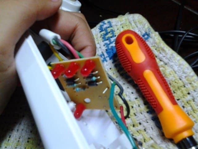
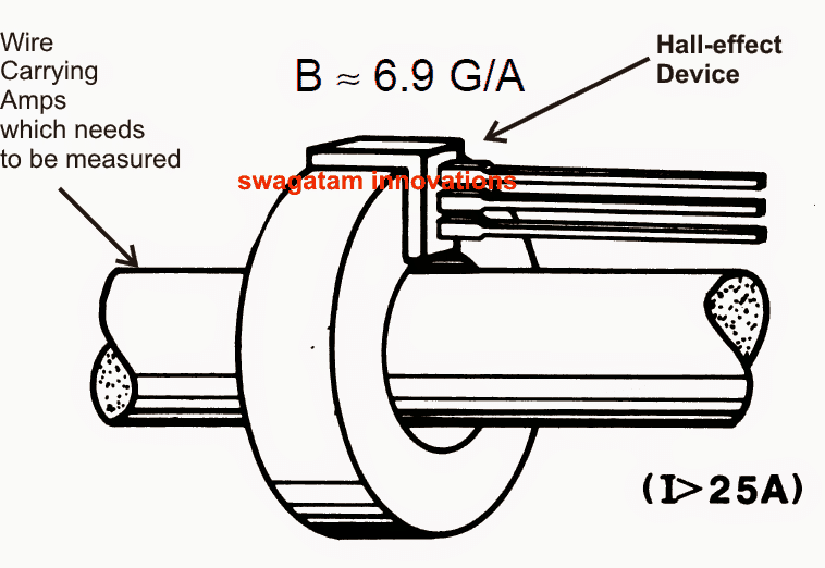 The equivalent conversions made by the Hall-effect can be directly read by appropriately connecting its leads to a digital multimeter set at mV DC range.
The supply lead of the Hall-effect IC should be connected to a DC source as per its specifications.
Courtesy:
allegromicro.com/~/media/Files/Technical-Documents/an27702-Linear-Hall-Effect-Sensor-ICs.ashx
The equivalent conversions made by the Hall-effect can be directly read by appropriately connecting its leads to a digital multimeter set at mV DC range.
The supply lead of the Hall-effect IC should be connected to a DC source as per its specifications.
Courtesy:
allegromicro.com/~/media/Files/Technical-Documents/an27702-Linear-Hall-Effect-Sensor-ICs.ashx
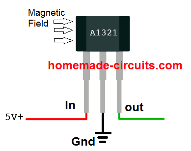

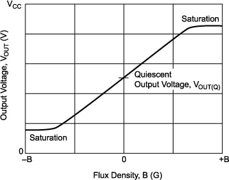
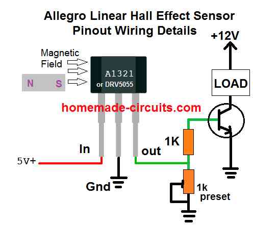 In this configuration, the hall effect sensor will convert a magnetic field within a specified proximity and will convert it into a linear analogue signal across its "out" pin.
This analogue signal can be easily used for driving a load or for feeding any desired switching circuit.
In this configuration, the hall effect sensor will convert a magnetic field within a specified proximity and will convert it into a linear analogue signal across its "out" pin.
This analogue signal can be easily used for driving a load or for feeding any desired switching circuit.
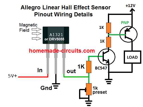
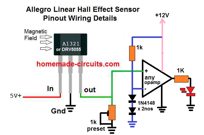 The DRV5055 hall effect sensor can be also integrated with an operational amplifier for getting the switch ON results in response to a magnetic proximity with the hall effect device.
Here the inverting input of the op amp is set to fixed reference of 1.2 V using two series 1N4148 diodes, while the non-inverting input of the op amp is configured with the output of the hall effect for the intended detection.
The 1k preset is used for setting up the switching threshold at which the op amp is supposed to switch, depending on the strength and the proximity level of the magnetic filed around the hall effect.
In the absence of a magnetic field, the hall effect sensor output remains below the set threshold of the op amp inputs.
As soon as the output from the hall effect goes above the non-inverting threshold of the op amp, as set by the preset and the reference level of the inverting input, the output of the op amp turn high, causing the LED to switch ON.
The LED could be replaced by another circuit stage for a switching ON some other desired load.
The DRV5055 hall effect sensor can be also integrated with an operational amplifier for getting the switch ON results in response to a magnetic proximity with the hall effect device.
Here the inverting input of the op amp is set to fixed reference of 1.2 V using two series 1N4148 diodes, while the non-inverting input of the op amp is configured with the output of the hall effect for the intended detection.
The 1k preset is used for setting up the switching threshold at which the op amp is supposed to switch, depending on the strength and the proximity level of the magnetic filed around the hall effect.
In the absence of a magnetic field, the hall effect sensor output remains below the set threshold of the op amp inputs.
As soon as the output from the hall effect goes above the non-inverting threshold of the op amp, as set by the preset and the reference level of the inverting input, the output of the op amp turn high, causing the LED to switch ON.
The LED could be replaced by another circuit stage for a switching ON some other desired load.
 Another Tilt switch Circuit
The above design could be much simplified as given below:
Another Tilt switch Circuit
The above design could be much simplified as given below:
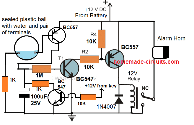
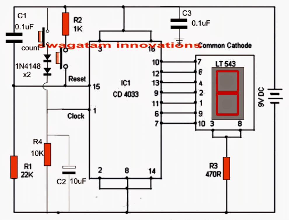
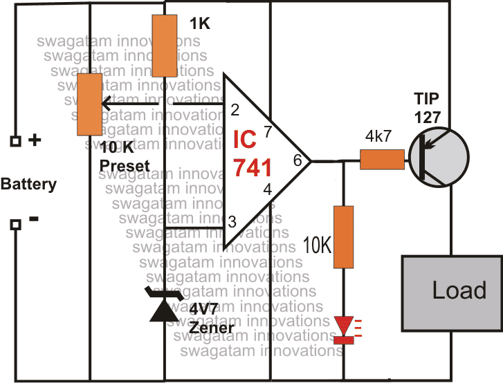
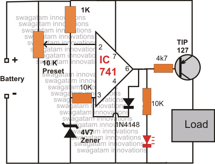 While setting the preset, make sure the feedback link stays (pin6 to pin3) disconnected, you can connect it back once the preset adjustment is complete.
 This is the vlf receiver circuit that I've upgraded and modified it senses ac fields lightening and even receives ship and aircraft radio too.
Now this is what the circuit looks like without the upgrades and modifications.
I've even used a gravity wave detector circuit added to it and also other experimental circuits
This is the vlf receiver circuit that I've upgraded and modified it senses ac fields lightening and even receives ship and aircraft radio too.
Now this is what the circuit looks like without the upgrades and modifications.
I've even used a gravity wave detector circuit added to it and also other experimental circuits

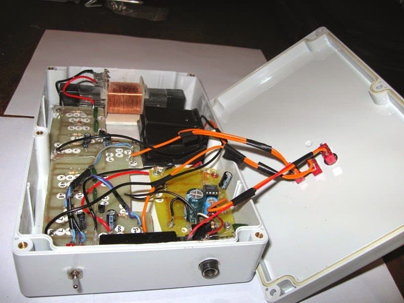
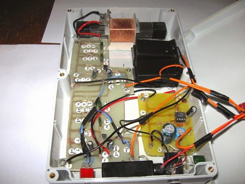
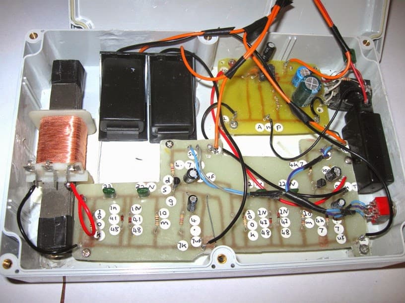
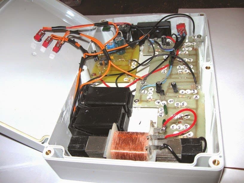
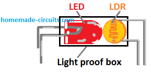
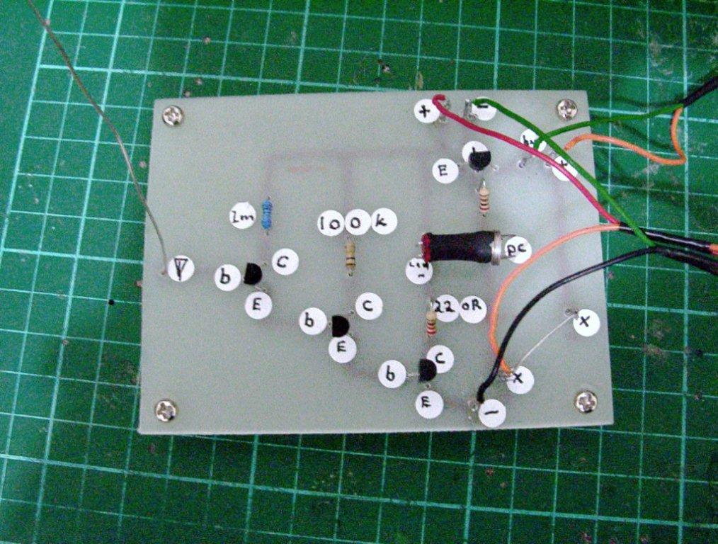 Hi Steven,Thanks,
when it comes to sensing light (as in our opto-coupler) I think LDRs are more efficient.
Moreover they are easy to handle and much cheaper.
I have a good and long experience with LDRs and found their working to be wonderfully well.
Thank you swagatam
I've just finished testing all my ldrs even the large on on the buzzer circuit built separate and not one of them works for me , strange considering ive never used these ldrs yet not for years and
When i measure them on my multimeter they register as 1k in the dark state and when i put light to then the resistance jumps to above 6k and if i use them in the separate buzzer circuit, the buzzer sounds loud with light shining on the ldr and also sounds loud still when they are dark.
At least 3 of my ldrs make the buzzer sound alter only slightly when i move light to it and away but thus still sounds loud and never silent even loud when i cover the ldr to block out all light
Hi Steven,
I don't quite agree with you.
There's definitely something's wrong either with yours LDRs or the procedures.
I have used LDRs in many of my projects - these devices are WONDERFUL.
Please do the following steps to check the LDR response:
Take the LDR, connect the multimeter prods to its legs, and hold it firmly with your fingers.
Let the ambient light fall over the LDR.
The meter will obviously show certain low value.
Now shift the "face" of the LDR somewhere towards the darker side.
You should immediately see a change in the reading of the meter (increased resistance).
Make the LDR face different light intensities by manually shifting its direction.
The meter should display different corresponding readings (resistance values).
This will convincingly prove the correct working of the LDR.
Also, at complete darkness the LDR should show INFINITE resistance.
If these conditions are not met, then definitely your LDR is a faulty one.
Once the above correct functions of the LDR is confirmed, now you may configure it to the opto coupler.
Also remember the opto coupler should be housed inside a PERFECTLY LIGHT PROOF ENCLOSURE, otherwise it will behave erratically and produce wrong results.
Thanks swagatam
I'll retest the ldrs again let you know.
what are the chances of all of my ldrs being faulty even though i haven't used them all up in all the years ive had them they've been sitting in my parts drws for so long il get back to you ill also test the transistor for the buzzer circuit and see if that's ok to your right swagatam
I underestimated the ldrs super sensitivity.
first i blocked all light from it using my fingers, in a room that has some light in it and tonight i did a better test with the window blinds closed and less light
So i was in darkness and the buzzer circuit which i ran the ldrs to was ok transistor tested ok and the buzzer in the dark died down to nil in the dark so they wasn't faulty after all but the only failure i got was my largest cd photocell or ldr in the dark the buzzer was still sounding and
When i applied light to it it got louder also using my finger to block light wasn't so useful after all as even the light at its lowest still went through my fingers and the high sensitivity of the ldr made it easy detectable
Still so the light has to be blocked much more from entering the ldr , especially through my glass fingers , i have some info i collected some time ago scientists saying that parts of the hand emit light even though we cant see it do you think its the case to of using a finger to block light when it emits invisible light and the ldr still senses it to with your finger covering the ldr.
Hi Steven,
Thanks - The theory behind the emission of photons by human hands might be true, in fact all living beings emit photons to some levels, but are too low to practically detect.
The level of LDRs response to light is quite equal to our eyes.
It simply means that any light that is not visible to our eyes cannot be "visible" to the LDR.
As we know it is almost immpossible to contain light, water and air in our hand, therefore in your experiment, its only the ambient light which is passing through your hands and not because of anything that is being emitted from your hands.
The opto-coupler needs to be SEALED inside an OPAQUE enclosure to produce the optimum results.
Hi Steven,Thanks,
when it comes to sensing light (as in our opto-coupler) I think LDRs are more efficient.
Moreover they are easy to handle and much cheaper.
I have a good and long experience with LDRs and found their working to be wonderfully well.
Thank you swagatam
I've just finished testing all my ldrs even the large on on the buzzer circuit built separate and not one of them works for me , strange considering ive never used these ldrs yet not for years and
When i measure them on my multimeter they register as 1k in the dark state and when i put light to then the resistance jumps to above 6k and if i use them in the separate buzzer circuit, the buzzer sounds loud with light shining on the ldr and also sounds loud still when they are dark.
At least 3 of my ldrs make the buzzer sound alter only slightly when i move light to it and away but thus still sounds loud and never silent even loud when i cover the ldr to block out all light
Hi Steven,
I don't quite agree with you.
There's definitely something's wrong either with yours LDRs or the procedures.
I have used LDRs in many of my projects - these devices are WONDERFUL.
Please do the following steps to check the LDR response:
Take the LDR, connect the multimeter prods to its legs, and hold it firmly with your fingers.
Let the ambient light fall over the LDR.
The meter will obviously show certain low value.
Now shift the "face" of the LDR somewhere towards the darker side.
You should immediately see a change in the reading of the meter (increased resistance).
Make the LDR face different light intensities by manually shifting its direction.
The meter should display different corresponding readings (resistance values).
This will convincingly prove the correct working of the LDR.
Also, at complete darkness the LDR should show INFINITE resistance.
If these conditions are not met, then definitely your LDR is a faulty one.
Once the above correct functions of the LDR is confirmed, now you may configure it to the opto coupler.
Also remember the opto coupler should be housed inside a PERFECTLY LIGHT PROOF ENCLOSURE, otherwise it will behave erratically and produce wrong results.
Thanks swagatam
I'll retest the ldrs again let you know.
what are the chances of all of my ldrs being faulty even though i haven't used them all up in all the years ive had them they've been sitting in my parts drws for so long il get back to you ill also test the transistor for the buzzer circuit and see if that's ok to your right swagatam
I underestimated the ldrs super sensitivity.
first i blocked all light from it using my fingers, in a room that has some light in it and tonight i did a better test with the window blinds closed and less light
So i was in darkness and the buzzer circuit which i ran the ldrs to was ok transistor tested ok and the buzzer in the dark died down to nil in the dark so they wasn't faulty after all but the only failure i got was my largest cd photocell or ldr in the dark the buzzer was still sounding and
When i applied light to it it got louder also using my finger to block light wasn't so useful after all as even the light at its lowest still went through my fingers and the high sensitivity of the ldr made it easy detectable
Still so the light has to be blocked much more from entering the ldr , especially through my glass fingers , i have some info i collected some time ago scientists saying that parts of the hand emit light even though we cant see it do you think its the case to of using a finger to block light when it emits invisible light and the ldr still senses it to with your finger covering the ldr.
Hi Steven,
Thanks - The theory behind the emission of photons by human hands might be true, in fact all living beings emit photons to some levels, but are too low to practically detect.
The level of LDRs response to light is quite equal to our eyes.
It simply means that any light that is not visible to our eyes cannot be "visible" to the LDR.
As we know it is almost immpossible to contain light, water and air in our hand, therefore in your experiment, its only the ambient light which is passing through your hands and not because of anything that is being emitted from your hands.
The opto-coupler needs to be SEALED inside an OPAQUE enclosure to produce the optimum results.
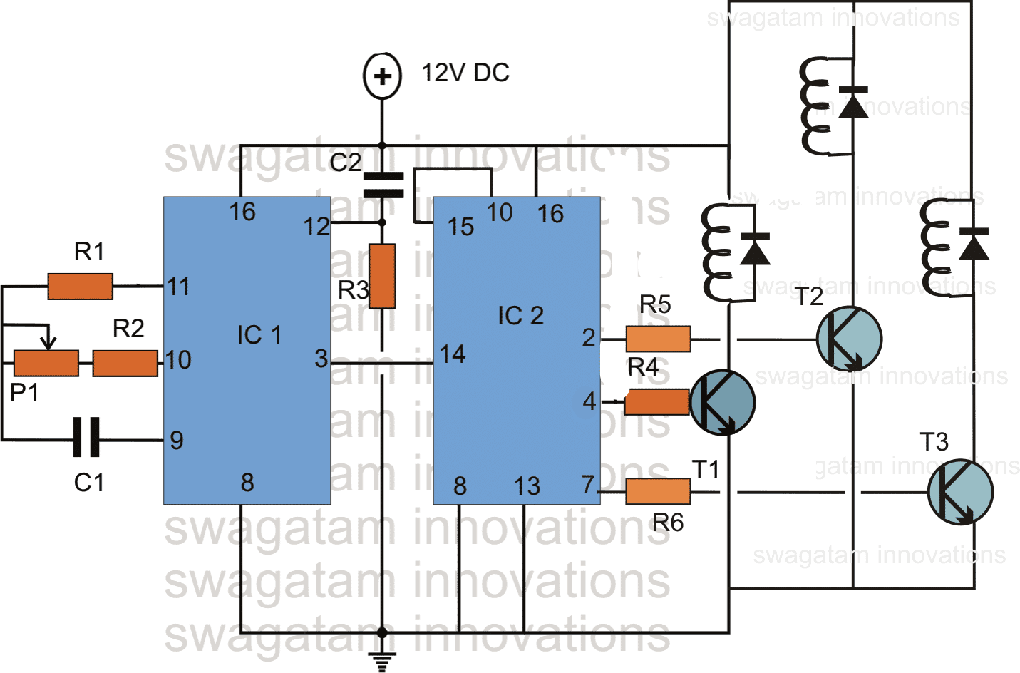

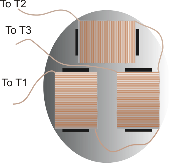 The following images of the built prototype were sent to me by one of the active readers of this blog, Mr.
Dan.
The following images of the built prototype were sent to me by one of the active readers of this blog, Mr.
Dan.

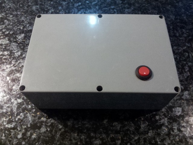

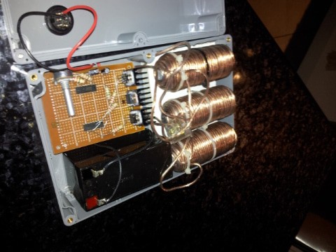
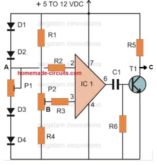
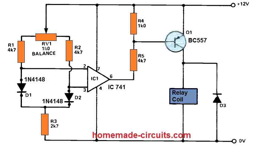 Ordinary silicon diodes may generate forward voltages of many 100 millivolts with current levels of one milliampere, with the actual voltage value being determined bythe current value and the properties of the individual diodes employed.
Nevertheless, all silicon diodes have a nearly similar temperature coefficient of around -2mV/ˇăC and may thus be employed as precise temperature-indicating sensors.
In the circuit, currents are allowed to pass via a couple oftemperature-sensing diodes (D1 and D2) via the RV1-R1-R2-R3 network.RV1 enables the similar specifications of the two currents to be modified over just a small range such that the diodes generate identical forward voltages onceboth the diodes areat the same temperature.
As a result, the differential or 'difference' voltage between the two diodes is precisely proportional to the temperature difference between them.
This difference voltage is applied to the input pins of the IC1 741, that is configured as a voltage comparator or differential voltage switch, and the output of the op-amp is applied to the relay through D1.
The operation is such that the relay activates as soon asD1's temperature exceeds that of D2. A 12 volt source is required to power the device.
When both sensor diodes (D1 and D2) are at identical warmth, RV1 is effectively changed such that the relay is turned off.
The relay canthen switch on oncethe temperature of D1 is elevated a tiny bit over that of D2: remember,this specificbehaviour may be tested at normal room temperature by just pressing D1 with finger, since body heat will provide the desired difference.
The relay connections can be used to control external devices.
Any 12 volt relay havinga coil resistance higher than 120 R will suffice.
This switch could be used to start a blower motor, as anexample, to guarantee that a basement or underground is properly preheated by some outside airflow when the outside air temperature is increased than the cellar or basement temperature.
It may also be used to control a solenoid valve, ensuring that a storage tank is automatically replenished directly from the warmer of two water sources, and so on.
Ordinary silicon diodes may generate forward voltages of many 100 millivolts with current levels of one milliampere, with the actual voltage value being determined bythe current value and the properties of the individual diodes employed.
Nevertheless, all silicon diodes have a nearly similar temperature coefficient of around -2mV/ˇăC and may thus be employed as precise temperature-indicating sensors.
In the circuit, currents are allowed to pass via a couple oftemperature-sensing diodes (D1 and D2) via the RV1-R1-R2-R3 network.RV1 enables the similar specifications of the two currents to be modified over just a small range such that the diodes generate identical forward voltages onceboth the diodes areat the same temperature.
As a result, the differential or 'difference' voltage between the two diodes is precisely proportional to the temperature difference between them.
This difference voltage is applied to the input pins of the IC1 741, that is configured as a voltage comparator or differential voltage switch, and the output of the op-amp is applied to the relay through D1.
The operation is such that the relay activates as soon asD1's temperature exceeds that of D2. A 12 volt source is required to power the device.
When both sensor diodes (D1 and D2) are at identical warmth, RV1 is effectively changed such that the relay is turned off.
The relay canthen switch on oncethe temperature of D1 is elevated a tiny bit over that of D2: remember,this specificbehaviour may be tested at normal room temperature by just pressing D1 with finger, since body heat will provide the desired difference.
The relay connections can be used to control external devices.
Any 12 volt relay havinga coil resistance higher than 120 R will suffice.
This switch could be used to start a blower motor, as anexample, to guarantee that a basement or underground is properly preheated by some outside airflow when the outside air temperature is increased than the cellar or basement temperature.
It may also be used to control a solenoid valve, ensuring that a storage tank is automatically replenished directly from the warmer of two water sources, and so on.


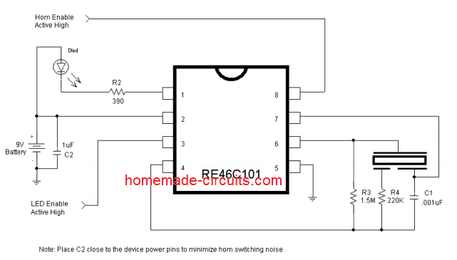 Courtesy - ww1.microchip.com/downloads/en/DeviceDoc/22163A.pdf
 The pin out diagram of the IC
 Simulation: A rough simulation of the discussed water level indicator circuit is shown below.
We can see how the LEDs light up sequentially in response to the increasing water level coming in contact with the respective sensor points inside the water tank
Simulation: A rough simulation of the discussed water level indicator circuit is shown below.
We can see how the LEDs light up sequentially in response to the increasing water level coming in contact with the respective sensor points inside the water tank
 Part List.
All LED resistors are 470 Ohms,
All gate input resistors are 2M2
All capacitors are 0.1 disc ceramic.
All the gates are CMOS NOT Gates
All LEDs are red 5mm, or as preferred by the maker.
Part List.
All LED resistors are 470 Ohms,
All gate input resistors are 2M2
All capacitors are 0.1 disc ceramic.
All the gates are CMOS NOT Gates
All LEDs are red 5mm, or as preferred by the maker.
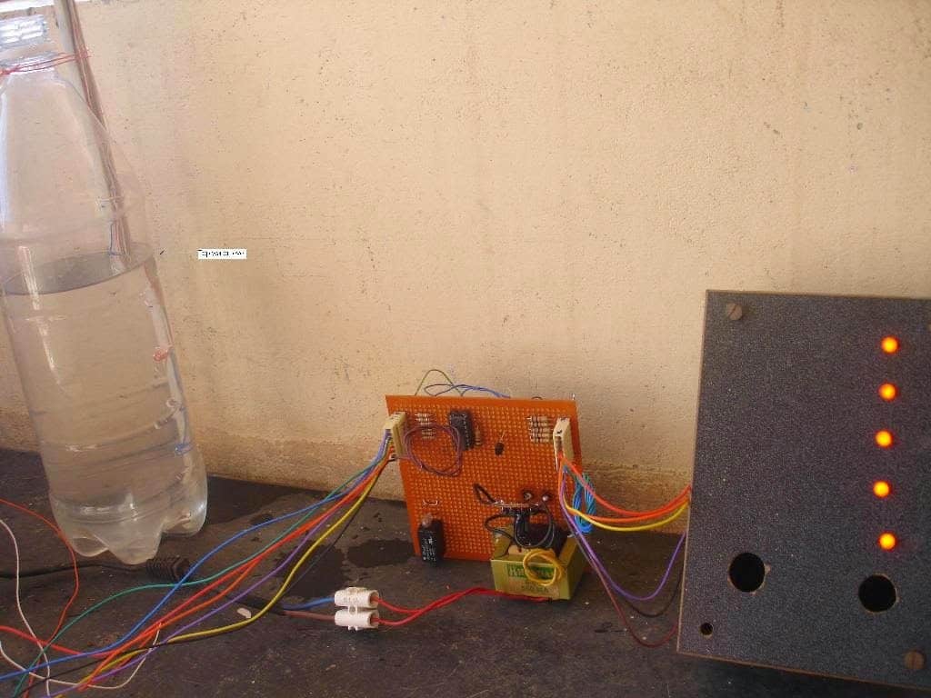
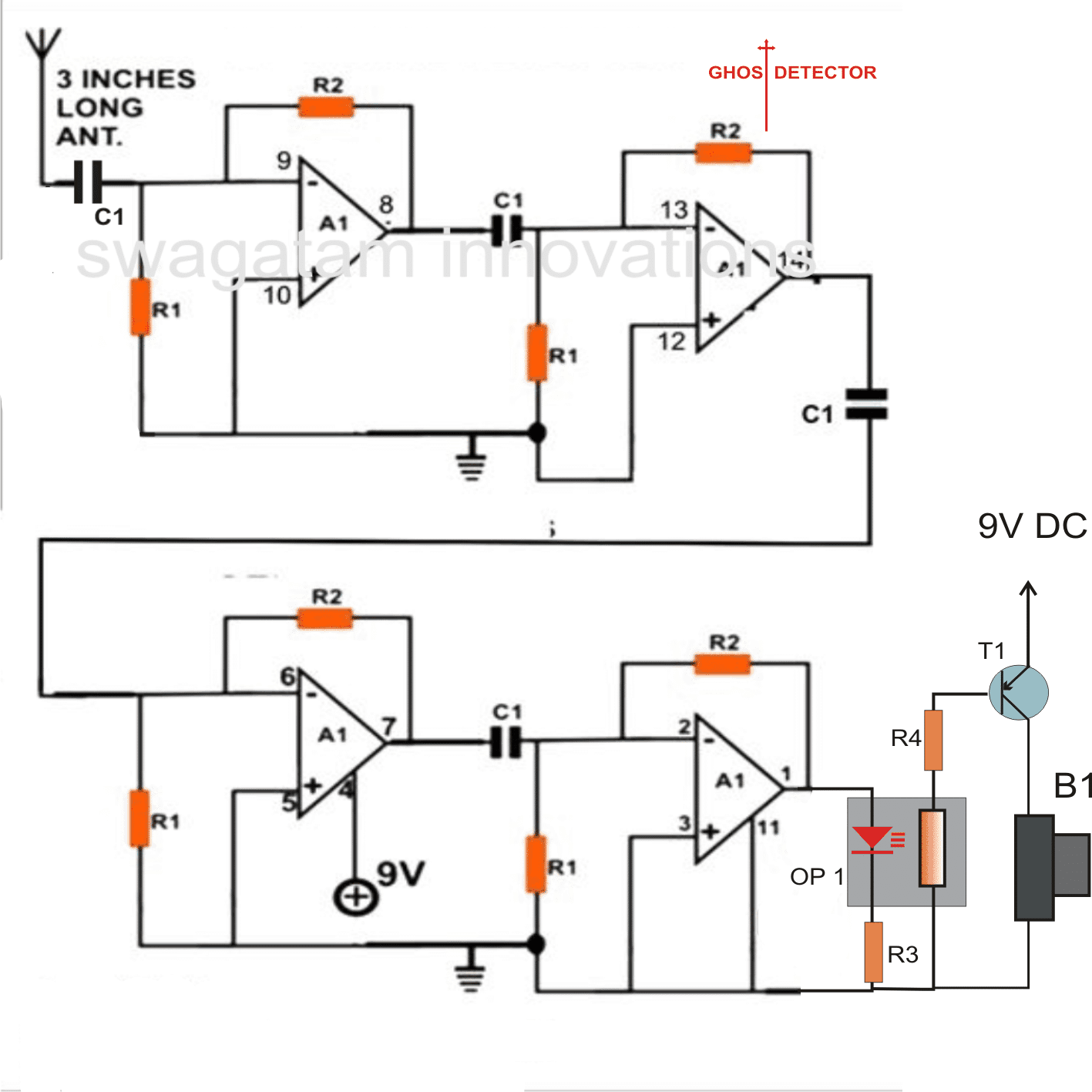 Referring to the figure, the opamps can be seen configured as hi gain non inverting amplifiers.
All the opamps are configured as high gain signal amplifiers.
Tiny electromagnetic or RF disturbances which are typically found being generated during the presence of ghosts or paranormal activities are instantly picked up by the antenna of the circuit and are fed to the input of the first opamp stage at pin #9.
The signals get instantly amplified and are transferred to the subsequent stages for further amplification and enhancement.
The output of the last opamp is connected to an opto-coupler.
The optocoupler is a homemade type, incorporating an LED and an LDR fixed such that their emitting and detecting surfaces are placed face to face inside a light proof enclosure.
Here, the optocoupler is used for sensing the LED illumination that may occur when a certain paranormal activity is sensed.
The illumination produced over the LED is tracked by the LDR whose resistance falls with the LED light.
The fall in the resistance of the LDR activates the connected transistor at the output, which in turn actuates a buzzer or a horn indicating a possible ghost intrusion.
The whole circuit may be built over a small piece of vero-board and should be strictly operated with a 9 volt battery.
The whole system may be enclosed inside a plastic box with the antenna kept protruding out of the box.
Referring to the figure, the opamps can be seen configured as hi gain non inverting amplifiers.
All the opamps are configured as high gain signal amplifiers.
Tiny electromagnetic or RF disturbances which are typically found being generated during the presence of ghosts or paranormal activities are instantly picked up by the antenna of the circuit and are fed to the input of the first opamp stage at pin #9.
The signals get instantly amplified and are transferred to the subsequent stages for further amplification and enhancement.
The output of the last opamp is connected to an opto-coupler.
The optocoupler is a homemade type, incorporating an LED and an LDR fixed such that their emitting and detecting surfaces are placed face to face inside a light proof enclosure.
Here, the optocoupler is used for sensing the LED illumination that may occur when a certain paranormal activity is sensed.
The illumination produced over the LED is tracked by the LDR whose resistance falls with the LED light.
The fall in the resistance of the LDR activates the connected transistor at the output, which in turn actuates a buzzer or a horn indicating a possible ghost intrusion.
The whole circuit may be built over a small piece of vero-board and should be strictly operated with a 9 volt battery.
The whole system may be enclosed inside a plastic box with the antenna kept protruding out of the box.
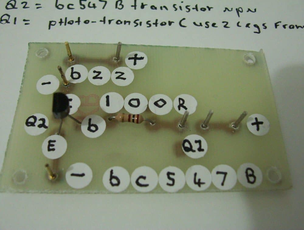
 Here is another picture of your optocoupler buzzer circuit for the ghost detector,
i used matrix pins on the board like i do with many circuits.this eliminates the job of having to take the board out of the circuit to resolder wires , buzz wires go to buzzer and q1 wires go to phototransistor, and the positive and negatives go to switch that runs to 9 volts battery to positive buzzer to positive in and negative of buzzer marked with the minus symbol.
Here is another picture of your optocoupler buzzer circuit for the ghost detector,
i used matrix pins on the board like i do with many circuits.this eliminates the job of having to take the board out of the circuit to resolder wires , buzz wires go to buzzer and q1 wires go to phototransistor, and the positive and negatives go to switch that runs to 9 volts battery to positive buzzer to positive in and negative of buzzer marked with the minus symbol.
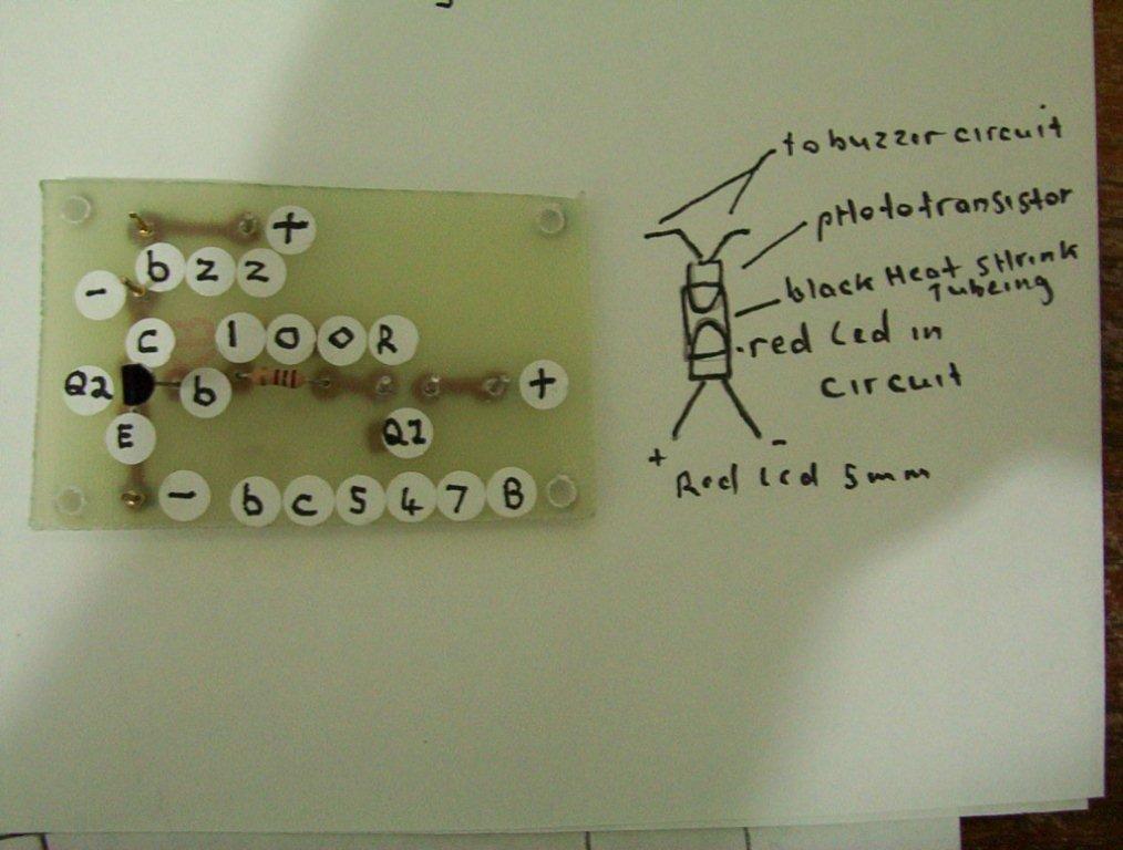 Hi Steven,
You have made this small circuit very special and all the effort you have put is amazing.
Thanks once again,
Swag
Thank you swagatam
It's your circuit your ideas I've upgraded thank you , now we have also the most sensitive lightening bolt detector for its size well have to test it out on a lightening bolt yet even though its very sensitive to the continuous sparking of the electric ignitor on the gas stove here it sounds awesome like receiving pulse rays well you should hear it different from just a hand held gas stove lighter with peizo electric sparks .
Hi Steven,
You have made this small circuit very special and all the effort you have put is amazing.
Thanks once again,
Swag
Thank you swagatam
It's your circuit your ideas I've upgraded thank you , now we have also the most sensitive lightening bolt detector for its size well have to test it out on a lightening bolt yet even though its very sensitive to the continuous sparking of the electric ignitor on the gas stove here it sounds awesome like receiving pulse rays well you should hear it different from just a hand held gas stove lighter with peizo electric sparks .
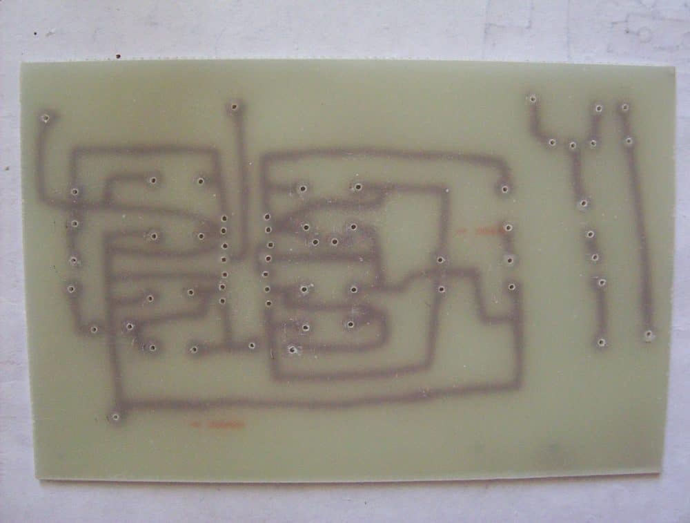 010jpg is the top view of the printed circuit board for the swagatam ghost detector circuit.
006 jpg is a close up of another ghost detector i just made notice the home made optocoupler using the fairchild photo transistor and led at each ends of a short length of black heatsink tubing.
ive changed the 10n ceramics to 10p to see what results i get when ive completed it allcouldn't resist the temptation to build another of your ghost detector circuits, so ill have backup in the case one fails
i hope you find some of these pictures better for your site or collection, this ones half finished so i have to do the wiring then put the rest of the box together as its a 3 peace one and maybe put the buzzer this time in a different area , etc etc i plan to build your ac sensor next to when i get to it ill email you all the details when i get to that one
010jpg is the top view of the printed circuit board for the swagatam ghost detector circuit.
006 jpg is a close up of another ghost detector i just made notice the home made optocoupler using the fairchild photo transistor and led at each ends of a short length of black heatsink tubing.
ive changed the 10n ceramics to 10p to see what results i get when ive completed it allcouldn't resist the temptation to build another of your ghost detector circuits, so ill have backup in the case one fails
i hope you find some of these pictures better for your site or collection, this ones half finished so i have to do the wiring then put the rest of the box together as its a 3 peace one and maybe put the buzzer this time in a different area , etc etc i plan to build your ac sensor next to when i get to it ill email you all the details when i get to that one
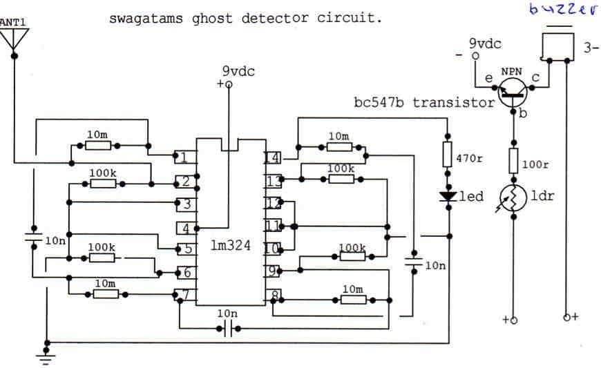 This is how i redraw circuits in a more simpler way using student version circuit maker , note the ic shape in its proper rectangle configuration , drawn using the trax maker tool and the pins stretched into there sizes, and shaped properly using the arrow tool, the numbering for the pins was done 1 number at a time using text tool function then dragged into the positions using the arrow in the program
READERS ARE REQUESTED TO SHARE THEIR EXPERIENCES WITH THIS DEVICE.
A PHOTO OR A VIDEO PROOF WILL BE GREATLY APPRECIATED....
This is how i redraw circuits in a more simpler way using student version circuit maker , note the ic shape in its proper rectangle configuration , drawn using the trax maker tool and the pins stretched into there sizes, and shaped properly using the arrow tool, the numbering for the pins was done 1 number at a time using text tool function then dragged into the positions using the arrow in the program
READERS ARE REQUESTED TO SHARE THEIR EXPERIENCES WITH THIS DEVICE.
A PHOTO OR A VIDEO PROOF WILL BE GREATLY APPRECIATED....
 The transistors are rigged as inverters, meaning when T1 switches, T2 is switched OFF and vice versa.
The transistors T1 is wired as a comparator and consists of an LDR across its base and the positive supply via a preset.
The LDR is used for sensing the ambient light conditions and is used for triggering T1 when the light level crosses a particular set threshold.
This threshold is set by the preset P1.
The use of two transistors particularly helps to reduce the hysteresis of the circuit which would have otherwise affected the circuit if only a single transistor would have been incorporated.
When T1 conducts, T2 is switched OFF ans so is the relay and the connected load or the light.
The opposite happens when the light over the LDR falls or when darkness sets in.
Parts List:
R1, R2, R3 = 4k7 1/4 watt
VR1 = 10k preset
LDR = any small LDR with around 10k to 50k resistance in day light (under shade)
C1 = 470uF/25V
C2 = 10uF/25V
All diodes = 1N4007
T1, T2 = BC547
Relay = 12V, 400 ohms, 5 amp
Transformer = 0-12V/500mA or 1 amp
The transistors are rigged as inverters, meaning when T1 switches, T2 is switched OFF and vice versa.
The transistors T1 is wired as a comparator and consists of an LDR across its base and the positive supply via a preset.
The LDR is used for sensing the ambient light conditions and is used for triggering T1 when the light level crosses a particular set threshold.
This threshold is set by the preset P1.
The use of two transistors particularly helps to reduce the hysteresis of the circuit which would have otherwise affected the circuit if only a single transistor would have been incorporated.
When T1 conducts, T2 is switched OFF ans so is the relay and the connected load or the light.
The opposite happens when the light over the LDR falls or when darkness sets in.
Parts List:
R1, R2, R3 = 4k7 1/4 watt
VR1 = 10k preset
LDR = any small LDR with around 10k to 50k resistance in day light (under shade)
C1 = 470uF/25V
C2 = 10uF/25V
All diodes = 1N4007
T1, T2 = BC547
Relay = 12V, 400 ohms, 5 amp
Transformer = 0-12V/500mA or 1 amp
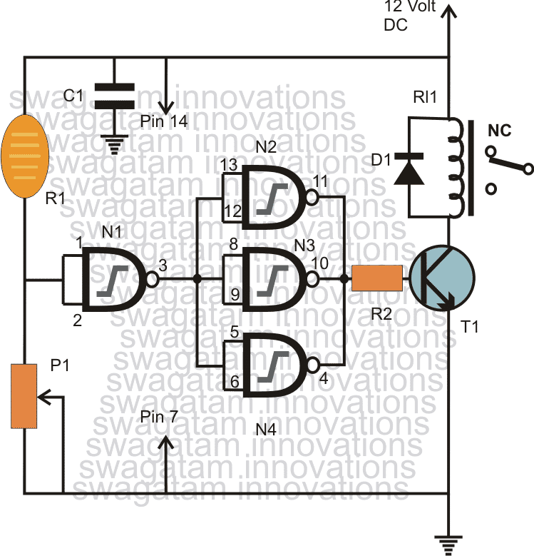 Each of the gates are formed into inverters by shorting its both the inputs together, so that the input logic level of the gates now get effectively reversed at thie outputs.
Though a single NAND gate would be enough for implementing the actions, three gates have been engaged as buffers for getting better results and in a view of utilizing all of them as in any case three of them would be left idle.
The gate which is responsible for the sensing can be seen accompanied with the light sensing device LDR wired across its input and the positive via a variable resistor.
This variable resistor is used for setting the triggering point of the gate when the light falling over the LDR reaches the desired specified intensity.
As this happens, the gate input goes high, the output consequently becomes low making the outputs of the buffer gates high.
The result is the triggering of the transistor and the relay assembly.
The connected load over the relay now flips into the intended actions.
Each of the gates are formed into inverters by shorting its both the inputs together, so that the input logic level of the gates now get effectively reversed at thie outputs.
Though a single NAND gate would be enough for implementing the actions, three gates have been engaged as buffers for getting better results and in a view of utilizing all of them as in any case three of them would be left idle.
The gate which is responsible for the sensing can be seen accompanied with the light sensing device LDR wired across its input and the positive via a variable resistor.
This variable resistor is used for setting the triggering point of the gate when the light falling over the LDR reaches the desired specified intensity.
As this happens, the gate input goes high, the output consequently becomes low making the outputs of the buffer gates high.
The result is the triggering of the transistor and the relay assembly.
The connected load over the relay now flips into the intended actions.
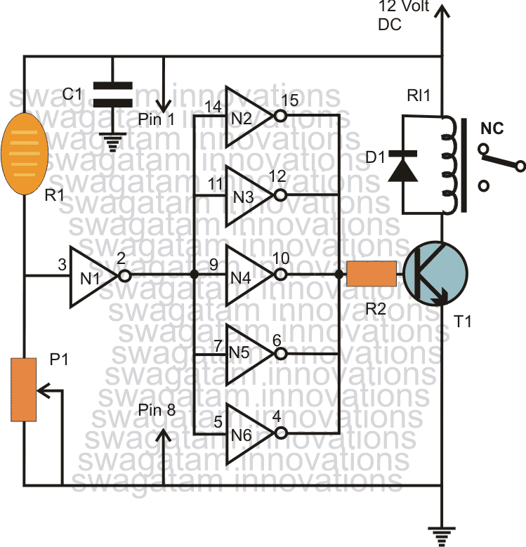 The above actions are exactly replicated using the IC 4049 which is also wired with similar configuration and is quite explanatory.
Parts List
R1 = Any LDR with resistance of around 10k to 50k in day light (under shade)
P1 = 1M preset
C1 = 0.1uF ceramic disc
R2 = 10k 1/4 watt
T1 = BC547
D1 = 1N4007
Relay = 12V, 400 ohm 5 amp
ICs = IC 4093 as in the first example or IC 4049 as in the second example
The above actions are exactly replicated using the IC 4049 which is also wired with similar configuration and is quite explanatory.
Parts List
R1 = Any LDR with resistance of around 10k to 50k in day light (under shade)
P1 = 1M preset
C1 = 0.1uF ceramic disc
R2 = 10k 1/4 watt
T1 = BC547
D1 = 1N4007
Relay = 12V, 400 ohm 5 amp
ICs = IC 4093 as in the first example or IC 4049 as in the second example
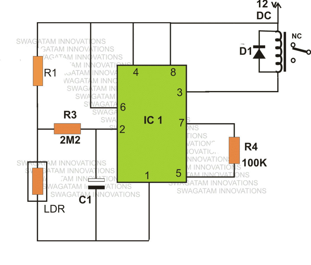 Video Clip demonstrating the practical operation of the above IC555 based day night automatic lamp circuit
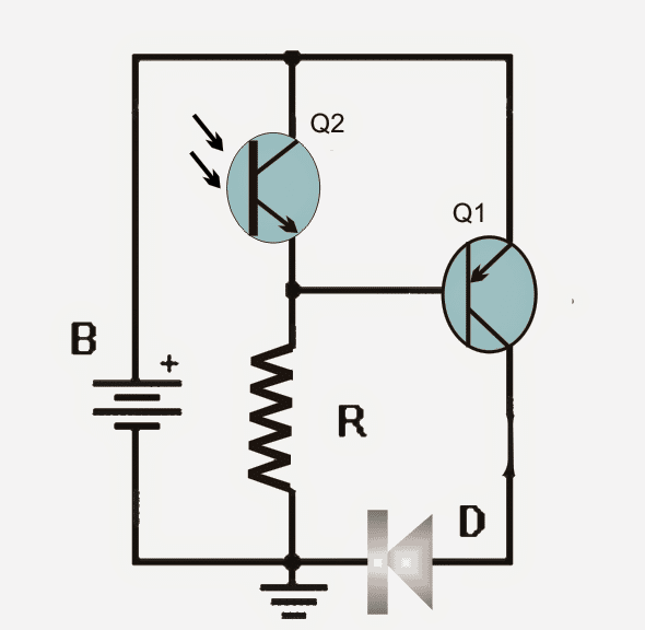
 The Q1 base resistor is actually a photo-resistor with the number ORP12. In the absence of light, the resistance of the photo-resistor is high, this causes Q1 to conduct and Q2 is remains shut off.
As the incident light on the photo-resistor OPR12 increases, its resistance falls to a point, until Q1 switches OFF and Q2 switches ON hard, activating the relay coil.In order to reset the circuit we can use the given push-button.
The freewheeling diode connected across the relay coil is to protect the transistor from relay coil reverse EMF spikes, and this diode could be any silicon diode such as the 1N4148 or 1N41007.
The Q1 base resistor is actually a photo-resistor with the number ORP12. In the absence of light, the resistance of the photo-resistor is high, this causes Q1 to conduct and Q2 is remains shut off.
As the incident light on the photo-resistor OPR12 increases, its resistance falls to a point, until Q1 switches OFF and Q2 switches ON hard, activating the relay coil.In order to reset the circuit we can use the given push-button.
The freewheeling diode connected across the relay coil is to protect the transistor from relay coil reverse EMF spikes, and this diode could be any silicon diode such as the 1N4148 or 1N41007.
 Referring the figure, we see a rather simple design made around a single active component which is the IC 555.
Other than the IC, the circuit just includes a few cheap passive components like resistors and capacitors.
We are familiar the two important modes of operation of the IC 555, which are the astable and the monostable multivibrator mode, however the IC is laid down in a rather unusual fashion, quite like a comparator.
Referring the figure, we see a rather simple design made around a single active component which is the IC 555.
Other than the IC, the circuit just includes a few cheap passive components like resistors and capacitors.
We are familiar the two important modes of operation of the IC 555, which are the astable and the monostable multivibrator mode, however the IC is laid down in a rather unusual fashion, quite like a comparator.
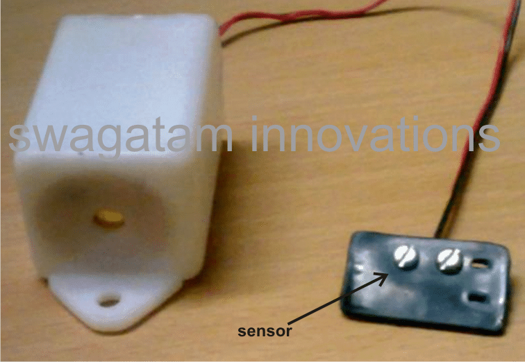
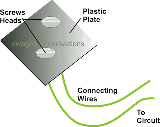 The wires from the screws should be carefully terminated to the relevant points on the circuit.
The circuit must be hosed inside a suitable plastic enclosure along with the buzzer and the battery.
Parts List
R1 = 1M, R2 = 100K,
P1 = 1M preset, can be replaced with a 1M fixed resistor
IC = 555, C1 = 10uF/25V,
The wires from the screws should be carefully terminated to the relevant points on the circuit.
The circuit must be hosed inside a suitable plastic enclosure along with the buzzer and the battery.
Parts List
R1 = 1M, R2 = 100K,
P1 = 1M preset, can be replaced with a 1M fixed resistor
IC = 555, C1 = 10uF/25V,
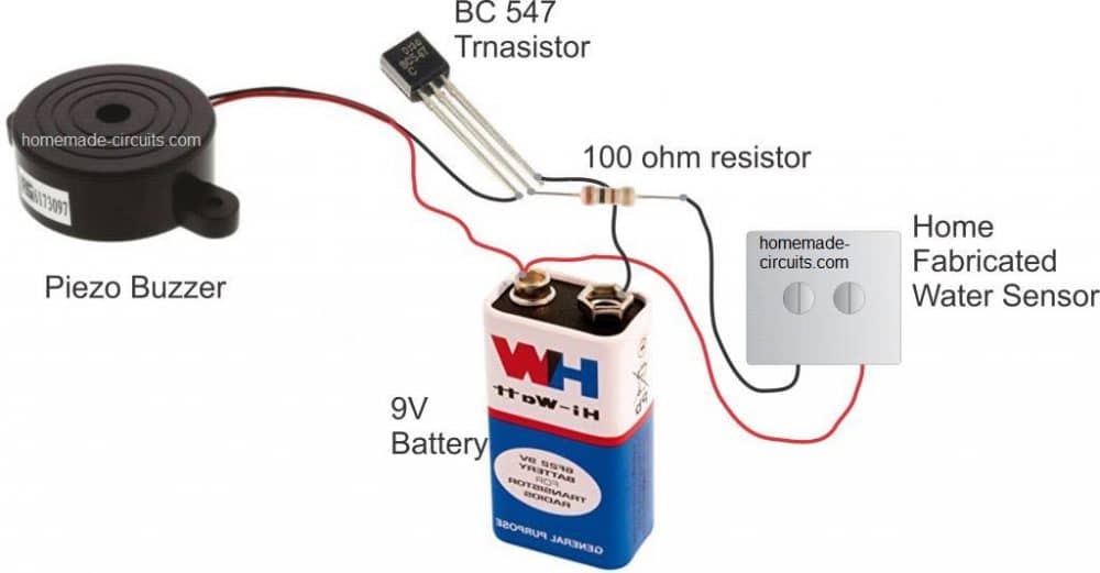 The working of the above circuit is rather simple.
When water droplets or rain droplets fall on the sensor device, made using screw heads, the water bridges across the screw heads allowing small electrical current to pass across the metal, triggering the base of the transistor.
As soon as this happens, the transistor begins conducting and amplifies the conduction across its collector/emitter terminals.
This results in the switching ON of the connected buzzer which now begins buzzing or beeping indicating the commencement of rain outside, and warning the user regarding the same.
The working of the above circuit is rather simple.
When water droplets or rain droplets fall on the sensor device, made using screw heads, the water bridges across the screw heads allowing small electrical current to pass across the metal, triggering the base of the transistor.
As soon as this happens, the transistor begins conducting and amplifies the conduction across its collector/emitter terminals.
This results in the switching ON of the connected buzzer which now begins buzzing or beeping indicating the commencement of rain outside, and warning the user regarding the same.
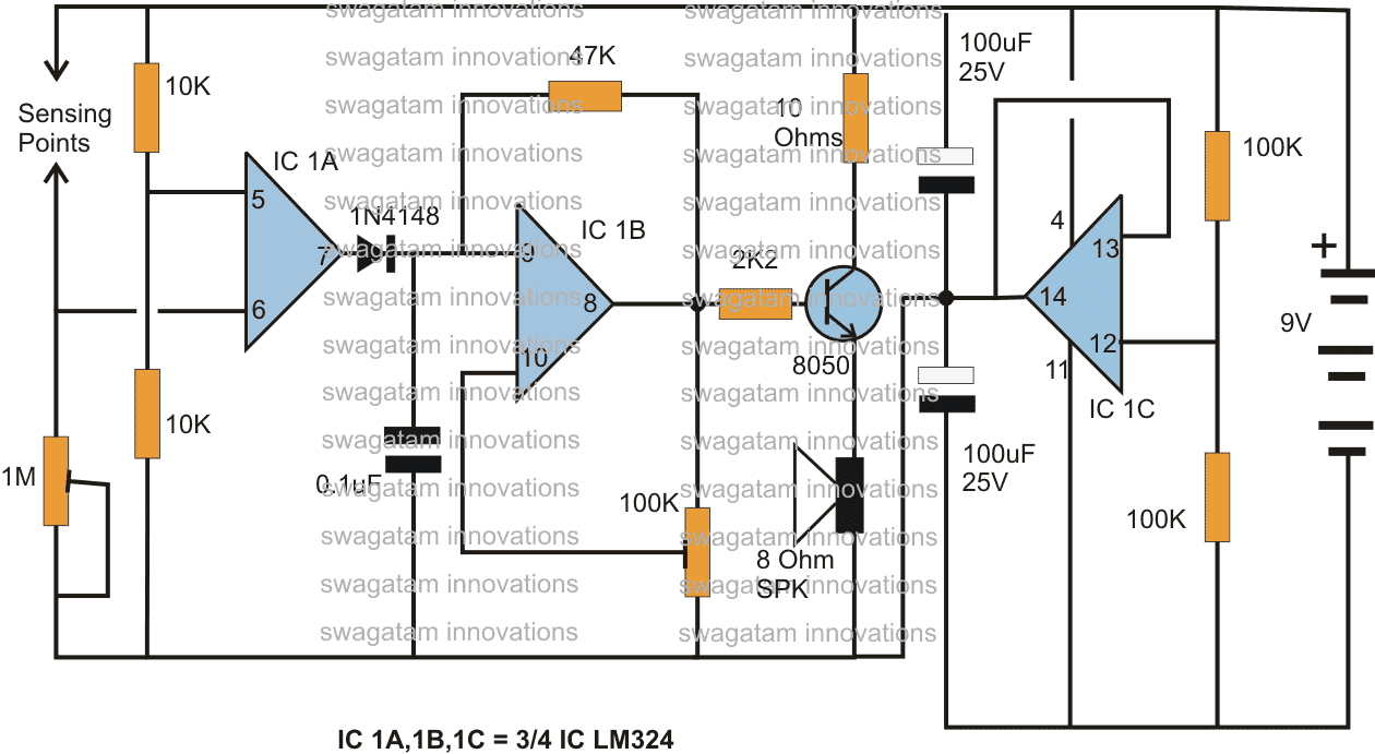
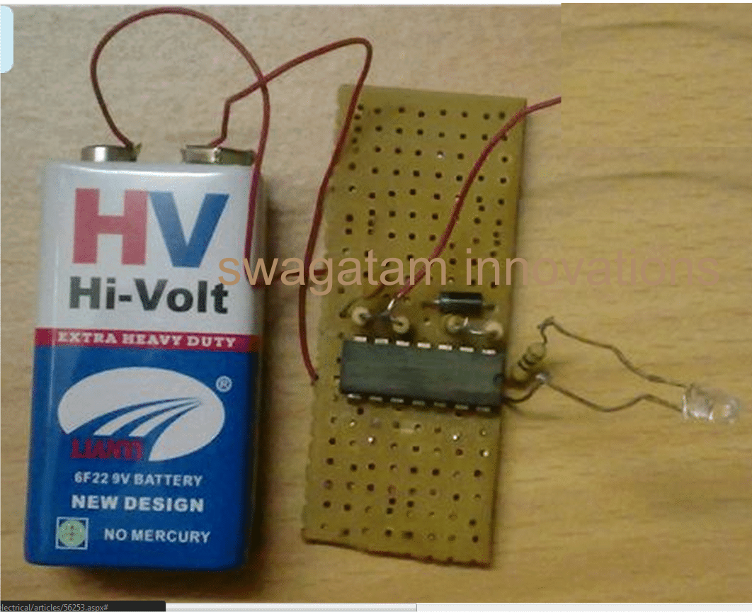 The circuit is basically high gain non inverting amplifier which is configured using a few opamps and a few other inexpensive passive electronic components.
Just a couple of opamps have been incorporated here from the IC 324 for the required operations.
The circuit is basically high gain non inverting amplifier which is configured using a few opamps and a few other inexpensive passive electronic components.
Just a couple of opamps have been incorporated here from the IC 324 for the required operations.
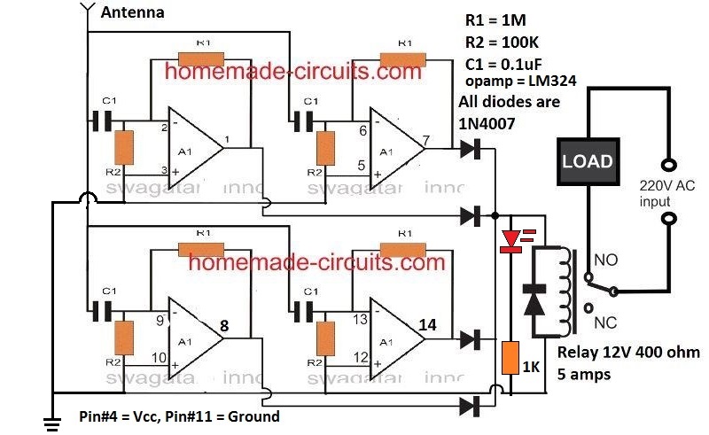
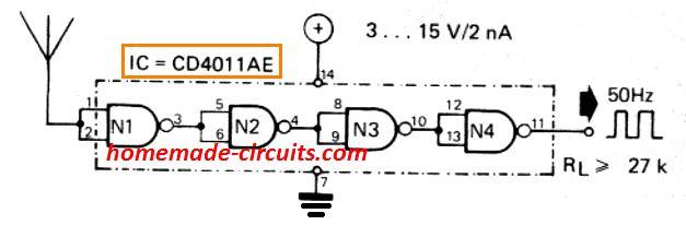 The first gate (N1) detects the 220 V or 120 V AC hum radiated by the mains grid electrical line.
You must take care not to keep the NAND gate inputs far away from various other sources of RF interference su ch as amplifier outputs, etc.
A copper wire with a length of 2 to 3 cm will be adequate to serve like an antenna for picking up the 50 Hz or 60 Hz hum and to process the signal into a correspnding level of square wave output.
The output may show a risetime of about 20 ns at the output of gate N4. Based on the circumstances, one or two gates can often be eliminated.
The current consumption of the complete CD 4011 IC is extremely minimal hence a 4.5 V battery employed as the power supply may be equivalent to almost the normal shelf life of th battery.
The first gate (N1) detects the 220 V or 120 V AC hum radiated by the mains grid electrical line.
You must take care not to keep the NAND gate inputs far away from various other sources of RF interference su ch as amplifier outputs, etc.
A copper wire with a length of 2 to 3 cm will be adequate to serve like an antenna for picking up the 50 Hz or 60 Hz hum and to process the signal into a correspnding level of square wave output.
The output may show a risetime of about 20 ns at the output of gate N4. Based on the circumstances, one or two gates can often be eliminated.
The current consumption of the complete CD 4011 IC is extremely minimal hence a 4.5 V battery employed as the power supply may be equivalent to almost the normal shelf life of th battery.
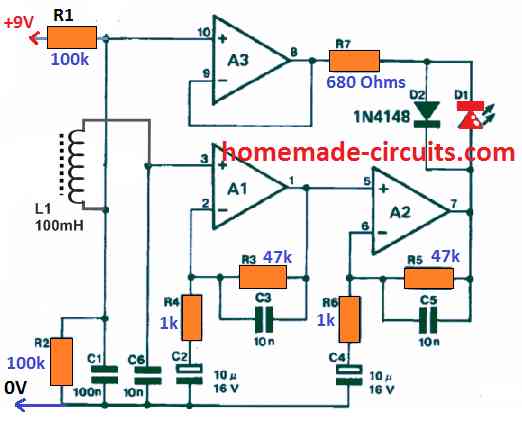 A current-carrying conductor generates a magnetic field and holds a minute voltage in L1, which is amplified through opamps A1 and A2.
Capacitors C2 to C5 occupy a value that makes sure maximum amplification in A1 and A2 with signals about 50 Hz.
Throughout the positive half-waves of the AC network, D1 stays lit.
A current-carrying conductor generates a magnetic field and holds a minute voltage in L1, which is amplified through opamps A1 and A2.
Capacitors C2 to C5 occupy a value that makes sure maximum amplification in A1 and A2 with signals about 50 Hz.
Throughout the positive half-waves of the AC network, D1 stays lit.
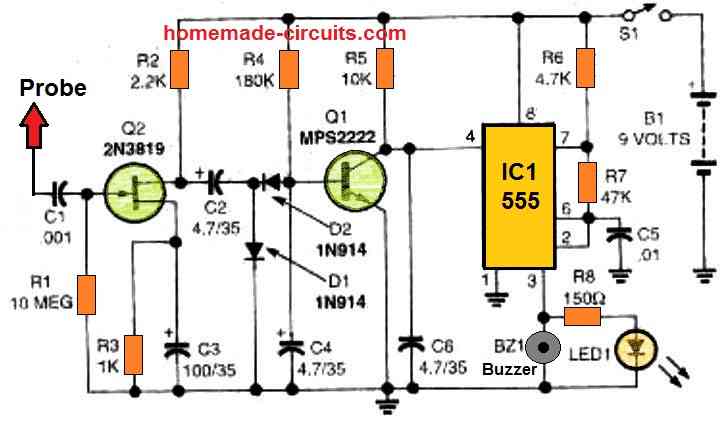 D2 rectifies the clamp output such that only negative voltages impact Q2. R4 typically switches on that transistor.
However,while the clamp is active, Q2 switches off.
Pin 4 (the reset line) of IC1 is freed when Q2 is turned off.
R5 provides a positive voltage, allowing IC1 to start oscillating.
A piezoelectric buzzer and an LED are driven by the output of IC1 (pin 3).
R8 controls the current flowing to LED1. R6, R7, and C5 determine the frequency at which I C1oscillates.
Install the PC board into the enclosure to ensure that no parts interfere with BZ1, S1, LED1, or B1. With the help of thebelow overlay diagramas a reference, hookup from those elements to the PC board.
While wiring BZ1, the black lead, including the negative terminal of B1 and the cathode of LED, is connected to the common ground.
D2 rectifies the clamp output such that only negative voltages impact Q2. R4 typically switches on that transistor.
However,while the clamp is active, Q2 switches off.
Pin 4 (the reset line) of IC1 is freed when Q2 is turned off.
R5 provides a positive voltage, allowing IC1 to start oscillating.
A piezoelectric buzzer and an LED are driven by the output of IC1 (pin 3).
R8 controls the current flowing to LED1. R6, R7, and C5 determine the frequency at which I C1oscillates.
Install the PC board into the enclosure to ensure that no parts interfere with BZ1, S1, LED1, or B1. With the help of thebelow overlay diagramas a reference, hookup from those elements to the PC board.
While wiring BZ1, the black lead, including the negative terminal of B1 and the cathode of LED, is connected to the common ground.
 The supply for the current circuit is provided directly from the mains which happen across R1 and P1.
Two reference voltages are given by the 15 V steady-state voltage generated by R2, C1, C-2, D1 and D2.
Using a preset reference level of the mains voltage, these two voltages are compared in A1 and A2 from the IC LM358. If the subsequent mains become less than 210 V, D7 will illuminate.
When the reading is more than 250 V, the light on D8 will be switched on.
If neither of them lights up, T1 turns on and allows D4 to be lit.
This only means the mains voltage is in the safe operating limits.
The supply for the current circuit is provided directly from the mains which happen across R1 and P1.
Two reference voltages are given by the 15 V steady-state voltage generated by R2, C1, C-2, D1 and D2.
Using a preset reference level of the mains voltage, these two voltages are compared in A1 and A2 from the IC LM358. If the subsequent mains become less than 210 V, D7 will illuminate.
When the reading is more than 250 V, the light on D8 will be switched on.
If neither of them lights up, T1 turns on and allows D4 to be lit.
This only means the mains voltage is in the safe operating limits.
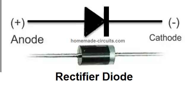 The main properties of a rectifier diode are as follows:
A diode has two terminals namely anode and cathode.
In a rectifier diode, the cathode side terminal is marked with a while band,
In a rectifier diode, current can flow only in one direction, that is from anode, towards cathode.
Current cannot flow the opposite.
It means, the diode will conduct only when a positive DC is connected to the anode, and negative DC is applied to the cathode.
If this polarity is reversed, the diode will not conduct, and will block the current.
Due to this property, rectifier diodes are normally used for rectification of AC to DC.
Meaning, when an alternating current is applied to the anode of the diode, it allows only the positive half cycles to pass to the cathode side and blocks the negative cycle, and in this way the AC is rectified to DC by the diode.
A rectifier diode being a semiconductor device, will always create a drop of around 0.6 V across its anode and cathode terminals.
Meaning, when a voltage is applied at anode, the cathode will produce a voltage which may be 0.6 V less than the voltage applied at the anode.
The main properties of a rectifier diode are as follows:
A diode has two terminals namely anode and cathode.
In a rectifier diode, the cathode side terminal is marked with a while band,
In a rectifier diode, current can flow only in one direction, that is from anode, towards cathode.
Current cannot flow the opposite.
It means, the diode will conduct only when a positive DC is connected to the anode, and negative DC is applied to the cathode.
If this polarity is reversed, the diode will not conduct, and will block the current.
Due to this property, rectifier diodes are normally used for rectification of AC to DC.
Meaning, when an alternating current is applied to the anode of the diode, it allows only the positive half cycles to pass to the cathode side and blocks the negative cycle, and in this way the AC is rectified to DC by the diode.
A rectifier diode being a semiconductor device, will always create a drop of around 0.6 V across its anode and cathode terminals.
Meaning, when a voltage is applied at anode, the cathode will produce a voltage which may be 0.6 V less than the voltage applied at the anode.
 Out of the two power supply applications of the diode, the full wave version is the more efficient one since it converts both the cycles of the AC into DC, while the single diode version converts only the half AC waves into DC.
The bridge rectifier connected with a transformer and without a filter capacitor can also be used as a stable 100 Hz frequency source or a 100 Hz frequency oscillator.
Out of the two power supply applications of the diode, the full wave version is the more efficient one since it converts both the cycles of the AC into DC, while the single diode version converts only the half AC waves into DC.
The bridge rectifier connected with a transformer and without a filter capacitor can also be used as a stable 100 Hz frequency source or a 100 Hz frequency oscillator.
 However, since the output is a DC, this can be diode application circuit can be used only for appliances that can work with AC and DC both, for example, electric shavers, LED lamps, heaters, electric motors, electric iron, soldering iron etc.
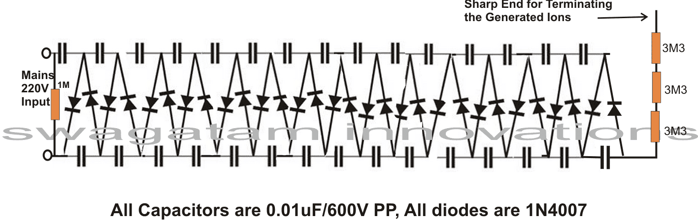 This configuration mainly uses the rectification and blocking feature of the diode, and the charge multiplying feature of the capacitors, to form a high negative voltage generator circuit which can be used for purifying the air around you!
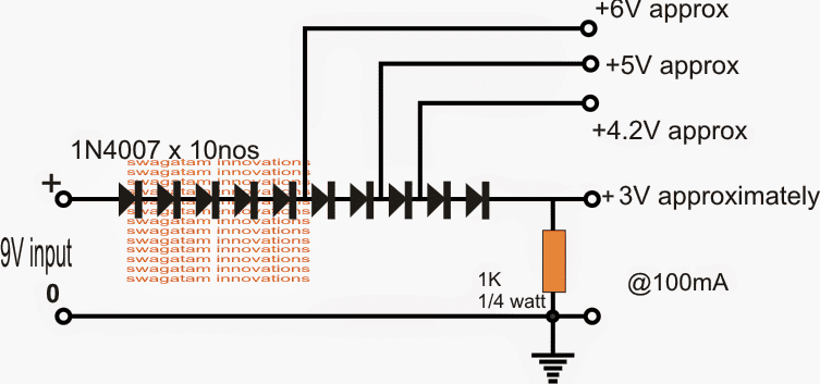 For example, if a 3.3 V is required from a 5 V source this can be easily achieved by adding a few series rectifier diodes at the output of the 5 V source.
Since each diode drops around 0. 6 V, it means 2 nos of diodes would be just enough for getting the required 3.3 V from a 5V supply.
For example, if a 3.3 V is required from a 5 V source this can be easily achieved by adding a few series rectifier diodes at the output of the 5 V source.
Since each diode drops around 0. 6 V, it means 2 nos of diodes would be just enough for getting the required 3.3 V from a 5V supply.
 Here we can see, many diodes are used in series to control the output from a solar panel to match the battery charging voltage.
The diodes drop the solar panel voltage in steps so that the voltage levels can be selected from low to high, as the sunlight goes down, thus making sure that the higher panel specifications does not cause any problems, and it is made compatible with any desired battery simply by switching a handful of rectifier diodes in series.
Here we can see, many diodes are used in series to control the output from a solar panel to match the battery charging voltage.
The diodes drop the solar panel voltage in steps so that the voltage levels can be selected from low to high, as the sunlight goes down, thus making sure that the higher panel specifications does not cause any problems, and it is made compatible with any desired battery simply by switching a handful of rectifier diodes in series.
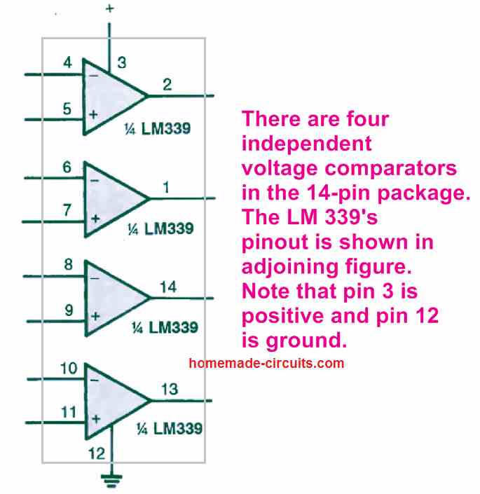
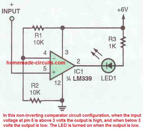 In the next figure above we can find how the IC LM339 can be configured as a non-inverting comparator-circuit .
The inverting input pin4 of the fixed with 3V reference by the voltage divider network formed by R1, R2. As long as the potential at pin 5 stays over 3 volts the output stays high, and the moment it drops below 3 volts the output of the IC turns low.
Remember, normally this should have caused the output to become high, but in IC LM339 the output turns low because of the internal transistor which inverts the response for the output of the IC.
The above condition causes the LED at the output to switch ON due to a low logic from the IC output.
In the next figure above we can find how the IC LM339 can be configured as a non-inverting comparator-circuit .
The inverting input pin4 of the fixed with 3V reference by the voltage divider network formed by R1, R2. As long as the potential at pin 5 stays over 3 volts the output stays high, and the moment it drops below 3 volts the output of the IC turns low.
Remember, normally this should have caused the output to become high, but in IC LM339 the output turns low because of the internal transistor which inverts the response for the output of the IC.
The above condition causes the LED at the output to switch ON due to a low logic from the IC output.
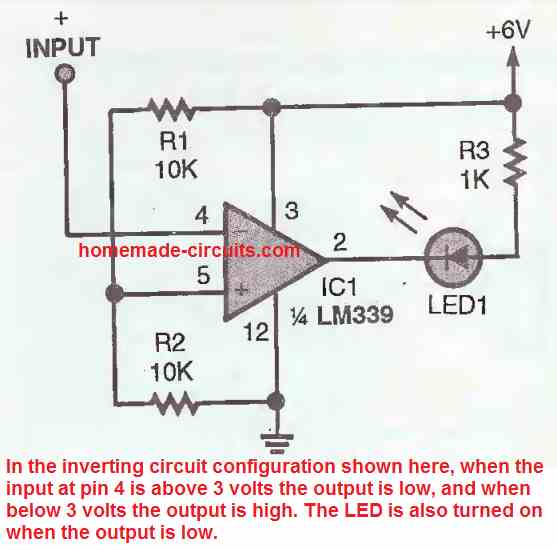 An LM339 inverting comparator circuit diagram can be witnessed in the figure above.
Here pin5 of the IC is fixed with a reference voltage of 3 V by the voltage divider formed by R1 and R2.
As long as the potential at pin 4 of the IC is higher than 3 volts, the output of the IC stays low, but the moment it goes below below 3 volts, the output switches to low logic.
The condition again causes the LED to switch ON due to the low logic from the IC output.
An LM339 inverting comparator circuit diagram can be witnessed in the figure above.
Here pin5 of the IC is fixed with a reference voltage of 3 V by the voltage divider formed by R1 and R2.
As long as the potential at pin 4 of the IC is higher than 3 volts, the output of the IC stays low, but the moment it goes below below 3 volts, the output switches to low logic.
The condition again causes the LED to switch ON due to the low logic from the IC output.
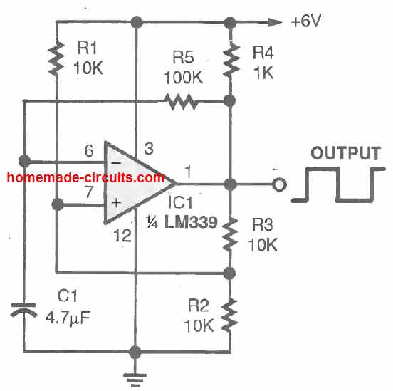 These are selected so that the LM339 circuit oscillates at a frequency of about 1.5 Hz.
If you reduce the value of any one of the RC components will cause an increase in the output frequency of the oscillator.
If you do the opposite will cause the oscillator frequency to reduce.
These are selected so that the LM339 circuit oscillates at a frequency of about 1.5 Hz.
If you reduce the value of any one of the RC components will cause an increase in the output frequency of the oscillator.
If you do the opposite will cause the oscillator frequency to reduce.
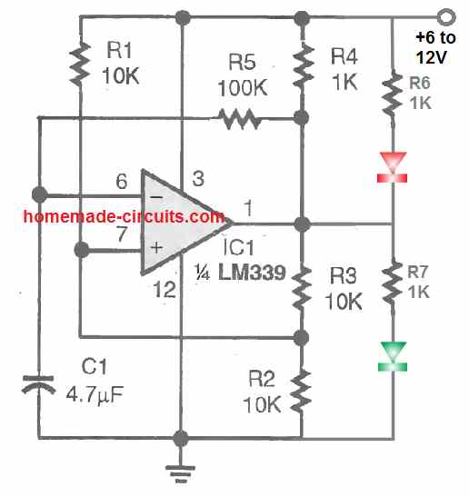 A flashing LED always looks more attractive than a solidly lit ones, and that is precisely what happens if the oscillator circuit is configured as given in the above figure.
Here the LEDs oscillate and turn ON/OFF alternately.
A flashing LED always looks more attractive than a solidly lit ones, and that is precisely what happens if the oscillator circuit is configured as given in the above figure.
Here the LEDs oscillate and turn ON/OFF alternately.
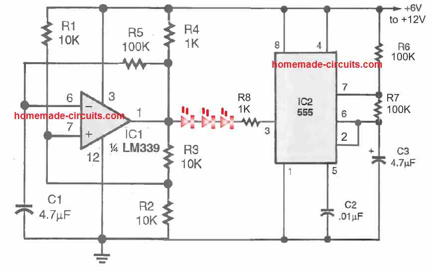 The above IC LM339 circuit can be used to create even more impressive looking LED strobe light blinker which intermittently flashes and then turns OFF, then again turns ON , flashes intermittently and then turns OFF.
This effect is achieved by integrating a IC 555 astable oscillator with the output of the LM339 oscillator circuit.
The LM339 provide the slow ON/OFF square wave pulse to the LED that causes LED to switch ON/OFF at moderately slow erate, while the IC 555 strobes the flashing LEDs into to rapidly switching ON/OFF pulses.
The LEDs can be 20 ma high bright RED or white LEDs.
To get a dual color strobe light, you an add another string of LED (green) connected parallel to the RED LEDs but in the opposite direction (reverse polarity).
The above IC LM339 circuit can be used to create even more impressive looking LED strobe light blinker which intermittently flashes and then turns OFF, then again turns ON , flashes intermittently and then turns OFF.
This effect is achieved by integrating a IC 555 astable oscillator with the output of the LM339 oscillator circuit.
The LM339 provide the slow ON/OFF square wave pulse to the LED that causes LED to switch ON/OFF at moderately slow erate, while the IC 555 strobes the flashing LEDs into to rapidly switching ON/OFF pulses.
The LEDs can be 20 ma high bright RED or white LEDs.
To get a dual color strobe light, you an add another string of LED (green) connected parallel to the RED LEDs but in the opposite direction (reverse polarity).
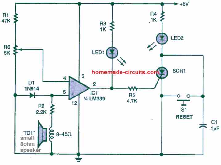 A tiny 8 ohm speaker is used as the vibration sensor while the opamp is configured in the non-inverting comparator mode.
When the speaker detect a vibration, it develops a voltage difference at pin5 of the IC that may exceed the reference voltage at pin4 as set by the preset R6. This cause the output of the op amp to go high momentarily, triggering the SCR ON, and the SCR LED lights up indicating the presence of the vibration on the speaker.
Initially when there's no vibration on the speaker, the potential at pin5 of the IC remains lower than the pin4 reference voltage, which causes the output of the opamp to remain low, and the SCR remains switched OFF.
The SCR can be any low voltage low current SCR.
The R6 preset must be set carefully so that the potential of pin4 is hardly 0.3 V higher than the pin5 potential.
A tiny 8 ohm speaker is used as the vibration sensor while the opamp is configured in the non-inverting comparator mode.
When the speaker detect a vibration, it develops a voltage difference at pin5 of the IC that may exceed the reference voltage at pin4 as set by the preset R6. This cause the output of the op amp to go high momentarily, triggering the SCR ON, and the SCR LED lights up indicating the presence of the vibration on the speaker.
Initially when there's no vibration on the speaker, the potential at pin5 of the IC remains lower than the pin4 reference voltage, which causes the output of the opamp to remain low, and the SCR remains switched OFF.
The SCR can be any low voltage low current SCR.
The R6 preset must be set carefully so that the potential of pin4 is hardly 0.3 V higher than the pin5 potential.
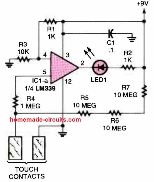 In this touch sensor circuit also, the LM339 opamp can be seen wired in the non-inverting mode.
The pin4 of the IC is clamped at some potential which is just lower than the pin5 potential.
Due to this the pin5 potential remains higher than the pin4 potential causing the output pin2 to remain high initially.
The situation causes the LED to remain shut off.
When the indicated touch pads are touched, causes the pin5 voltage to drop below the pin4 voltage, due to the ground potential delivered to pin5 through the finger contacts.
When this happens, the output of the op amp quickly turns low, and the LED gets the required ground potential for illuminating and indicating the existence of a touch contact on the touch plates.
So these a few LM339 circuits that you can build at home, if you have any more similar ideas do let us know through your comments, we will try to update them quickly in the above article.
In this touch sensor circuit also, the LM339 opamp can be seen wired in the non-inverting mode.
The pin4 of the IC is clamped at some potential which is just lower than the pin5 potential.
Due to this the pin5 potential remains higher than the pin4 potential causing the output pin2 to remain high initially.
The situation causes the LED to remain shut off.
When the indicated touch pads are touched, causes the pin5 voltage to drop below the pin4 voltage, due to the ground potential delivered to pin5 through the finger contacts.
When this happens, the output of the op amp quickly turns low, and the LED gets the required ground potential for illuminating and indicating the existence of a touch contact on the touch plates.
So these a few LM339 circuits that you can build at home, if you have any more similar ideas do let us know through your comments, we will try to update them quickly in the above article.
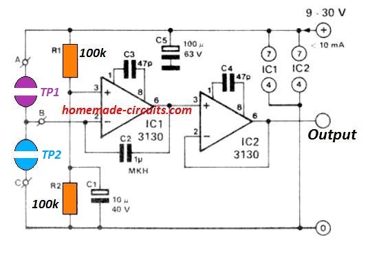 The best feature of this touch operated potentiometer circuit is that as soon as the finger contact is removed from the pad, the voltage magnitude then appearing at the output of IC1 is retained by the stored charge on C2.
On account of inevitable leakage currents in the capacitor, the output voltage will, eventually, start drifting by approximately 2 % each hour towards zero or towards the supply voltage, depending on which specific key pad had been touched last.
To ensure that the leakage current is as minimum as possible, it is important to keep the circuit away from humidity or dampness.
This is a crucial aspect that must be taken into account while implementing this design.
The best feature of this touch operated potentiometer circuit is that as soon as the finger contact is removed from the pad, the voltage magnitude then appearing at the output of IC1 is retained by the stored charge on C2.
On account of inevitable leakage currents in the capacitor, the output voltage will, eventually, start drifting by approximately 2 % each hour towards zero or towards the supply voltage, depending on which specific key pad had been touched last.
To ensure that the leakage current is as minimum as possible, it is important to keep the circuit away from humidity or dampness.
This is a crucial aspect that must be taken into account while implementing this design.
 Resistors R3 and R4 imitate the skin resistance; switches S1 and S2 supply the input potential to the IC1.
If you press the two switches together the output will stay unaffected and won't produce any variation in its existing value.
Capacitors C3 and C4 eliminate all possibility of the operational amplifier to go into an oscillation mode.
Resistors R3 and R4 imitate the skin resistance; switches S1 and S2 supply the input potential to the IC1.
If you press the two switches together the output will stay unaffected and won't produce any variation in its existing value.
Capacitors C3 and C4 eliminate all possibility of the operational amplifier to go into an oscillation mode.
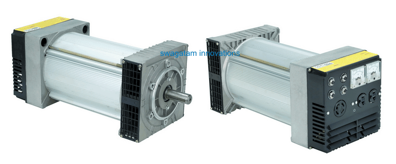 Instead of winding a vertical axis wind generator yourself, a simpler idea would be to configure the VAWT mechanism with a high watt generator or a dynamo through a correctly calculated gear or pulley/belt ratio.
For example, the above shown 10 kv dynamo has a specifications of generating 10000 watt at around 3600 RPM, which implies that if the a pulley ratio of 1:100 is configured, the dynamo would be able to produce the rated amount of power with the VAWT rotating at just around 36 RPM, which could be achieved perhaps even at wind speeds as low as 5km per hour.
Instead of winding a vertical axis wind generator yourself, a simpler idea would be to configure the VAWT mechanism with a high watt generator or a dynamo through a correctly calculated gear or pulley/belt ratio.
For example, the above shown 10 kv dynamo has a specifications of generating 10000 watt at around 3600 RPM, which implies that if the a pulley ratio of 1:100 is configured, the dynamo would be able to produce the rated amount of power with the VAWT rotating at just around 36 RPM, which could be achieved perhaps even at wind speeds as low as 5km per hour.
 The figure above shows a simple vertical axis wind turbine model, the vertical helical turbine is designed to capture wind flow on one half of its span while allow free flow on the other half, causing the propeller to initiate a rotational movement with high torque.
Being vertical in its positioning the VAWT does not rely on wind directions unlike the traditional horizontal axis wind turbines.
This advantage makes the VAWT sustain its operations under all wind conditions regardless of its direction of flow.
The central vertical axis of the turbine can be seen attached with a gigantic flywheel, which is supposed to be a lot bigger than the wheel attached with the generator shaft.
The bigger the ratio, the bigger would be the conversion even at minimal wind speeds.
With a ratio of 1:100, the generator could be expected to be generating at its full capacity and specification, with the VAWT moving at a meager 50 RPM or even less.
This speed could be in turn achieved at wind speeds not exceeding 5 to 10 miles per hour.
The figure above shows a simple vertical axis wind turbine model, the vertical helical turbine is designed to capture wind flow on one half of its span while allow free flow on the other half, causing the propeller to initiate a rotational movement with high torque.
Being vertical in its positioning the VAWT does not rely on wind directions unlike the traditional horizontal axis wind turbines.
This advantage makes the VAWT sustain its operations under all wind conditions regardless of its direction of flow.
The central vertical axis of the turbine can be seen attached with a gigantic flywheel, which is supposed to be a lot bigger than the wheel attached with the generator shaft.
The bigger the ratio, the bigger would be the conversion even at minimal wind speeds.
With a ratio of 1:100, the generator could be expected to be generating at its full capacity and specification, with the VAWT moving at a meager 50 RPM or even less.
This speed could be in turn achieved at wind speeds not exceeding 5 to 10 miles per hour.
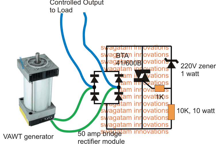 In the above figure the generator output is applied to a high current triac shunt regulator network through a 50 amp bridge rectifier module.
The value of the zener diode determines the control threshold, which is shown as 220V in the diagram.
It means under no circumstances the voltage from the generator can exceed the 220V mark, and if it does the excess power is simply shunted or shorted to ground via the triac.
This ensures a controlled rotation of the generator even at formidable wind speeds keeping the entire system stabilized and safe.
If the generator used is a 3 phase type of generator, the shunt regulator shown above could be replaced with a 3 phase shunt regulator using SCRs.
If you have any doubts regarding the discussed vertical axis wind turbine generator circuit, do feel free to express them through comments
In the above figure the generator output is applied to a high current triac shunt regulator network through a 50 amp bridge rectifier module.
The value of the zener diode determines the control threshold, which is shown as 220V in the diagram.
It means under no circumstances the voltage from the generator can exceed the 220V mark, and if it does the excess power is simply shunted or shorted to ground via the triac.
This ensures a controlled rotation of the generator even at formidable wind speeds keeping the entire system stabilized and safe.
If the generator used is a 3 phase type of generator, the shunt regulator shown above could be replaced with a 3 phase shunt regulator using SCRs.
If you have any doubts regarding the discussed vertical axis wind turbine generator circuit, do feel free to express them through comments
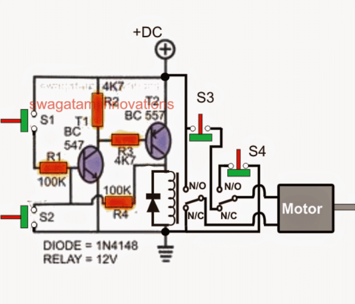
 The above Switch is to be used for S3, S4
Transistor T1, T2 along with the associated parts form a reliable latch circuit, S1 and S2 are ordinary push-to-ON switches, where S1 is rigged as the "set" button, and S2 as the reset button, which work for opening and closing the connected respectively.
S3 and S4 are fixed across the end travel points of the gate mechanism, such that the gate pushes these OFF each time it reaches the end destinations, and releases while it moves away from the destination or while the gate is in the course of its travel.
Assuming the gate to be in the closed position initially, we can expect the following scenario:
The above Switch is to be used for S3, S4
Transistor T1, T2 along with the associated parts form a reliable latch circuit, S1 and S2 are ordinary push-to-ON switches, where S1 is rigged as the "set" button, and S2 as the reset button, which work for opening and closing the connected respectively.
S3 and S4 are fixed across the end travel points of the gate mechanism, such that the gate pushes these OFF each time it reaches the end destinations, and releases while it moves away from the destination or while the gate is in the course of its travel.
Assuming the gate to be in the closed position initially, we can expect the following scenario:
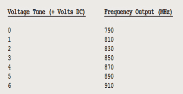 In our above discussion, a typical VCO has the ability of tuning between 790-910 MHz with a voltage tune from 0 to +6 VDC.
This turns out to approximately 20 MHz of tune/volt.
per volt.
Which means that, if you had the desire to "jam" the frequency ranges between 870-890 MHz, it would necessaite a +1 volt peak-to-peak triangle wave with a DC offset of +4 volts.
This might turn out to be a voltage signal sweeping between +4 and +5 VDC (referenced from ground), as well as might sweep the VCO's RF output between 870-890 MHz.
Having said this,, in practically, the voltage-to-frequency mappings are not this precisely crucial..
An additional important piece of the RF jammer sequence is the end stage RF power amplifier.
This might be considered as a a stage which isolates a mini RF input signal, say for example at +10 dBm (10 milliwatts), and expands it up to around +36 dBm (4 watts) and further.
The easy to get source of such amplifiers is from some discarded analog cellphones itself.
Some unused old cellphones (Motorola, Nokia, Uniden, etc.) may possibly employ a broadband RF power "hybrid" module which facilitates to make their construction much hassle free and scales-down.
These types of RF module equipment are quite wideband in terms of frequency, and is designed to comfortably enlarge RF signals lying beyond their specified range.
Enhancing the module's RF power control bias (Vapc) or Vdd voltage might additionally extract some more gain from these, but might also #blank# affect the expected life span of the power module.
The RF power module might require to be linked with a significant, and well polished heatsink and could necessiatate a cooling fan on higher power amplifiers.
In our above discussion, a typical VCO has the ability of tuning between 790-910 MHz with a voltage tune from 0 to +6 VDC.
This turns out to approximately 20 MHz of tune/volt.
per volt.
Which means that, if you had the desire to "jam" the frequency ranges between 870-890 MHz, it would necessaite a +1 volt peak-to-peak triangle wave with a DC offset of +4 volts.
This might turn out to be a voltage signal sweeping between +4 and +5 VDC (referenced from ground), as well as might sweep the VCO's RF output between 870-890 MHz.
Having said this,, in practically, the voltage-to-frequency mappings are not this precisely crucial..
An additional important piece of the RF jammer sequence is the end stage RF power amplifier.
This might be considered as a a stage which isolates a mini RF input signal, say for example at +10 dBm (10 milliwatts), and expands it up to around +36 dBm (4 watts) and further.
The easy to get source of such amplifiers is from some discarded analog cellphones itself.
Some unused old cellphones (Motorola, Nokia, Uniden, etc.) may possibly employ a broadband RF power "hybrid" module which facilitates to make their construction much hassle free and scales-down.
These types of RF module equipment are quite wideband in terms of frequency, and is designed to comfortably enlarge RF signals lying beyond their specified range.
Enhancing the module's RF power control bias (Vapc) or Vdd voltage might additionally extract some more gain from these, but might also #blank# affect the expected life span of the power module.
The RF power module might require to be linked with a significant, and well polished heatsink and could necessiatate a cooling fan on higher power amplifiers.
 The following image shows an overview of an old Radio Shack CT-1055 (Cat No.
17-1007A) 800 MHz band analog cellular phone.
The following image shows an overview of an old Radio Shack CT-1055 (Cat No.
17-1007A) 800 MHz band analog cellular phone.
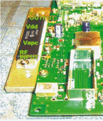 You can see the presence of the Hitachi PF0030 RF power amplifier IC module mounted over a heatsink, and ample heatsink compound being used in between the device and the heatsink.
In the discussed prototype the entire IC along with the heatsink was salvaged.
If you do not happen to have such an alanogue cellphone circuit with you, you could purchase it brand new from the market, the pinout details of the same may be witnessed below:
You can see the presence of the Hitachi PF0030 RF power amplifier IC module mounted over a heatsink, and ample heatsink compound being used in between the device and the heatsink.
In the discussed prototype the entire IC along with the heatsink was salvaged.
If you do not happen to have such an alanogue cellphone circuit with you, you could purchase it brand new from the market, the pinout details of the same may be witnessed below:
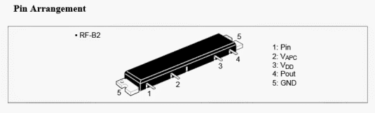 The following picture depicts an overview of the completed 800 MHz Cellular Phone Jammer unit
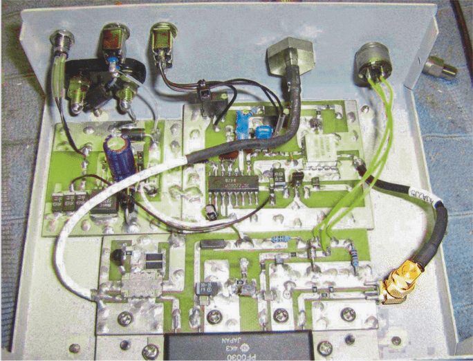 An alternate of the above may be witnessed below:
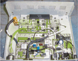
 10V regulated power supply for the above cellphone jammer stages
 Parts List
R1 = 3k3,
R2 = 100K,
R3 = 470 Ohms
C1 = 10 pF,C2 = 27 pF
C3 = 27pF,
C4 = 102 disc
C5 = 10uF/10V,
Mic = condenser mic
T1 = BC547
L1 = 3 to 4 turns of 22SWG super enamel copper wire, 5 to 7 mmdiameter, air corePlease refer the scanned image of the prototype for getting an idea regarding the coil dimensions.
Now let's discuss a few FM transmitter circuits which can be built using different configurations and features.
Parts List
R1 = 3k3,
R2 = 100K,
R3 = 470 Ohms
C1 = 10 pF,C2 = 27 pF
C3 = 27pF,
C4 = 102 disc
C5 = 10uF/10V,
Mic = condenser mic
T1 = BC547
L1 = 3 to 4 turns of 22SWG super enamel copper wire, 5 to 7 mmdiameter, air corePlease refer the scanned image of the prototype for getting an idea regarding the coil dimensions.
Now let's discuss a few FM transmitter circuits which can be built using different configurations and features.
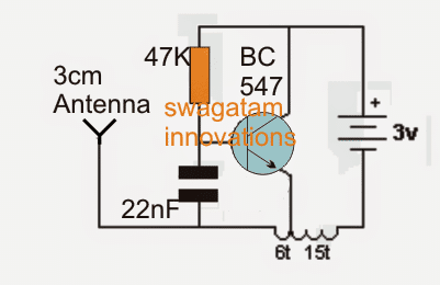
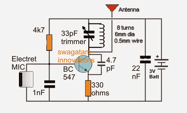
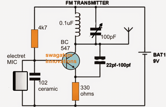
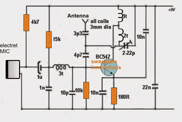
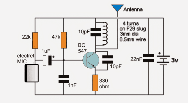
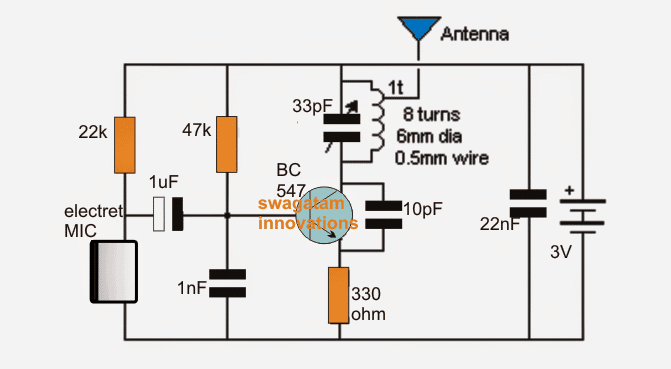
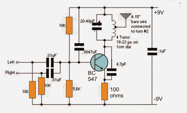
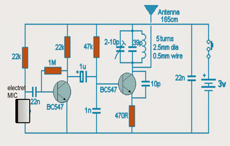 Five things that that make the circuit extremely good with it reception are:
The use of a fix capacitor in the tank circuit along with a adjustable trimmer.
A low value coupling capacitor with the MIC sufficient to handle the capacitive reactance of the MIC which may be around 4k at 3kHz.
A 1u coupler is included between the oscillator and the audio amplifier in order to make up for the low impedance rendered by the 47k base resistor.
The coil used is wound practically using super enameled copper wire which ensures higher efficiency than PCB etched type of coil.
The entire circuit could be compactly constructed over a small sized PCB for acquiring better stability and a drift free frequency response.
Five things that that make the circuit extremely good with it reception are:
The use of a fix capacitor in the tank circuit along with a adjustable trimmer.
A low value coupling capacitor with the MIC sufficient to handle the capacitive reactance of the MIC which may be around 4k at 3kHz.
A 1u coupler is included between the oscillator and the audio amplifier in order to make up for the low impedance rendered by the 47k base resistor.
The coil used is wound practically using super enameled copper wire which ensures higher efficiency than PCB etched type of coil.
The entire circuit could be compactly constructed over a small sized PCB for acquiring better stability and a drift free frequency response.
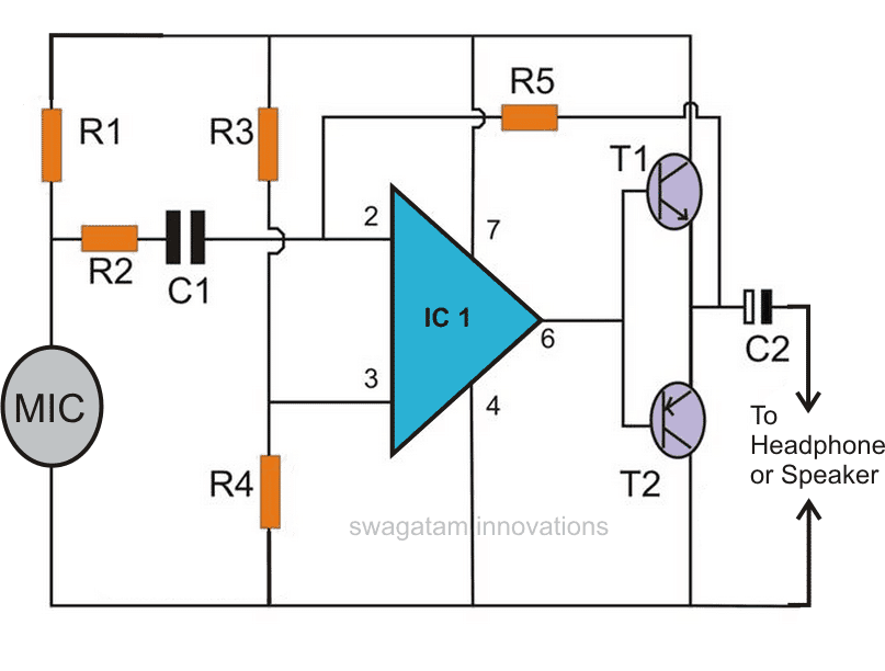 For the 741 circuit, the speaker is only positioned and used as the receiver and may be placed in some other room, where the eavesdropping may be intended to be carried out.
The linking of the speaker from the amplifier circuit may be done through wire connections, preferably by using thin wires and escorting the entire length up to the speaker in some hidden way, probably by laying it under the carpet or across the corners of the room.
For the wireless spy transmitter circuit everything becomes pretty simple and you just have to hide the transmitter circuit in some suitable place, like under the table, couch, sofa etc.
Parts List
R1 = 10K,
R2 = 10k,
R3, R4 = 27K,
R5 = 1.5 M,
C1 = 104,
C2 = 220uF/25V,
T1 = 188,
T2 = 187,
MIC = electret mic,
IC1 = 741,Power = 9 volt battery
Headphone = 64 Ohms, or a small speaker of 8 Ohms, 2 inches
For the 741 circuit, the speaker is only positioned and used as the receiver and may be placed in some other room, where the eavesdropping may be intended to be carried out.
The linking of the speaker from the amplifier circuit may be done through wire connections, preferably by using thin wires and escorting the entire length up to the speaker in some hidden way, probably by laying it under the carpet or across the corners of the room.
For the wireless spy transmitter circuit everything becomes pretty simple and you just have to hide the transmitter circuit in some suitable place, like under the table, couch, sofa etc.
Parts List
R1 = 10K,
R2 = 10k,
R3, R4 = 27K,
R5 = 1.5 M,
C1 = 104,
C2 = 220uF/25V,
T1 = 188,
T2 = 187,
MIC = electret mic,
IC1 = 741,Power = 9 volt battery
Headphone = 64 Ohms, or a small speaker of 8 Ohms, 2 inches
 Clearly, this may not be feasible, however the report does emphasize that the current in an inductor could quickly attain substantial and potentially dangerous magnitudes.
This formula merely is valid as long as the inductor remains below the saturation point.
As soon as the inductor core reaches saturation, the inductive concentration is unable to optimize the current rise.
Therefore the current rises very fast which is simply beyond the prediction range of the equation.
During the saturation, the current gets restricted at a value normally established by the series resistance and applied voltage.
In case of smaller inductors the increases in current through them is really fast, but they can retain significant levels of energy within a stipulated timeframe.
On the contrary, bigger inductor values may show sluggish current rise through, but these are unable to retain high levels of energy within the same stipulated time.
This effect can be witnessed in the second and third graphs, the former demonstrating rise in current in 10 ¦ĚH, 100 ¦ĚH, and 1 mH inductors when a 10V supply is utilized.
Clearly, this may not be feasible, however the report does emphasize that the current in an inductor could quickly attain substantial and potentially dangerous magnitudes.
This formula merely is valid as long as the inductor remains below the saturation point.
As soon as the inductor core reaches saturation, the inductive concentration is unable to optimize the current rise.
Therefore the current rises very fast which is simply beyond the prediction range of the equation.
During the saturation, the current gets restricted at a value normally established by the series resistance and applied voltage.
In case of smaller inductors the increases in current through them is really fast, but they can retain significant levels of energy within a stipulated timeframe.
On the contrary, bigger inductor values may show sluggish current rise through, but these are unable to retain high levels of energy within the same stipulated time.
This effect can be witnessed in the second and third graphs, the former demonstrating rise in current in 10 ¦ĚH, 100 ¦ĚH, and 1 mH inductors when a 10V supply is utilized.
 Graph 3 indicates the energy stored over time for inductors with the same values.
In the fourth graph we can see the current rise through the same inductors, by applying a 10 V although now a series resistance of 1 Ohm isinserted in series with the inductor.
Graph 3 indicates the energy stored over time for inductors with the same values.
In the fourth graph we can see the current rise through the same inductors, by applying a 10 V although now a series resistance of 1 Ohm isinserted in series with the inductor.
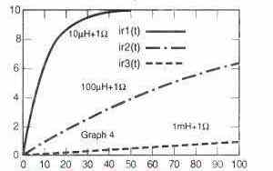
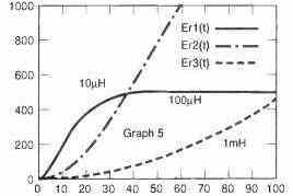 The fifth graph demonstrates the energy stored for the very same inductors.
Here, it is apparent that this current through the 10 ¦ĚH inductor soars rapidly towards the 10 A maximum value in roughly 50 ms.
However as a result of 1 ohm resistor it is able to retain only close to 500 millijoules.
Having said that, current through 100 ¦ĚH and 1 mH inductors rises and the stored energy tend to be reasonably unaffected with the series resistance across the same amount of time.
The fifth graph demonstrates the energy stored for the very same inductors.
Here, it is apparent that this current through the 10 ¦ĚH inductor soars rapidly towards the 10 A maximum value in roughly 50 ms.
However as a result of 1 ohm resistor it is able to retain only close to 500 millijoules.
Having said that, current through 100 ¦ĚH and 1 mH inductors rises and the stored energy tend to be reasonably unaffected with the series resistance across the same amount of time.
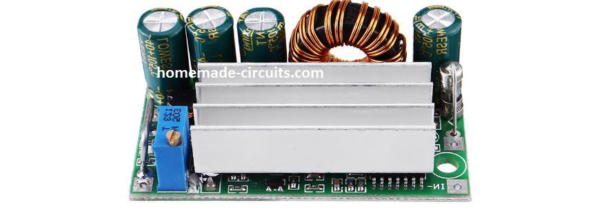 The power converter explained in this article employs the device TL 497A integrated circuit from Texas Instruments.
This particular IC facilitates excellent voltage regulation with minimal output noise to be accomplished pretty conveniently, and likewise ensures high conversion performance.
The power converter explained in this article employs the device TL 497A integrated circuit from Texas Instruments.
This particular IC facilitates excellent voltage regulation with minimal output noise to be accomplished pretty conveniently, and likewise ensures high conversion performance.
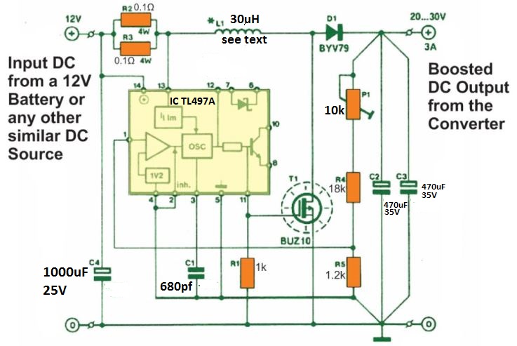 As soon as the transistor is switched off, the inductor reverts the stored magnetic energy, converting it into an electric current across the connected load via D1.
During this procedure, it is crucial to ensure that the transistor continues to be switched OFF for the period while the magnetic field on the inductor decays to zero.
In case this condition fails to implement, the current via the inductor soars up to the saturation level.
An avalanche effect subsequently results in the current to maximize pretty quickly.
The relative transistor control trigger ON time, or duty factor thus, should not be allowed to get to the unity level.
The maximum allowable duty factor relies, on various other aspects, around the output voltage.
This is because it decides the decaying rate of the magnetic field strength.
The highest output power that could be achieved from the converter is determined by the highest allowable peak current processed by the inductor, and the switching frequency of the driving signal.
The restricting elements here are primarily the saturation instant and the inductor's maximum tolerable ratings for the copper losses, as well as the peak current via the switching transistor (do not forget that a spike of a specific electrical energy level comes to the output during each switching pulse).
As soon as the transistor is switched off, the inductor reverts the stored magnetic energy, converting it into an electric current across the connected load via D1.
During this procedure, it is crucial to ensure that the transistor continues to be switched OFF for the period while the magnetic field on the inductor decays to zero.
In case this condition fails to implement, the current via the inductor soars up to the saturation level.
An avalanche effect subsequently results in the current to maximize pretty quickly.
The relative transistor control trigger ON time, or duty factor thus, should not be allowed to get to the unity level.
The maximum allowable duty factor relies, on various other aspects, around the output voltage.
This is because it decides the decaying rate of the magnetic field strength.
The highest output power that could be achieved from the converter is determined by the highest allowable peak current processed by the inductor, and the switching frequency of the driving signal.
The restricting elements here are primarily the saturation instant and the inductor's maximum tolerable ratings for the copper losses, as well as the peak current via the switching transistor (do not forget that a spike of a specific electrical energy level comes to the output during each switching pulse).
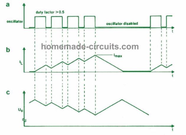 The step wise increase in the current as indicated in Fig.
2b is because of the oscillator signal duty factor which happens to be higher than 0.5.
As soon as the attained optimum current is reached, the oscillator gets deactivated, allowing the inductor to transfer its energy across the capacitors.
In this particular situation, the output voltage soars to a magnitude which is just high to ensure that the oscillator is switched OFF by means of IC pin 1. The output voltage now quickly falls, so that a fresh charge cycle is able to start and repeat the procedure.
However, sadly, the switching procedures discussed above will be combined with a comparatively large losses.
In a real life implementation, this issue can be remedied by setting up the on time (via C1) high enough to make sure that the current through the inductor never extends to the highest level in a single oscillator interval (see Fig.
3).
The remedy in such cases may be the incorporation of an air cored inductor, that features a reasonably minimal self-inductance.
The step wise increase in the current as indicated in Fig.
2b is because of the oscillator signal duty factor which happens to be higher than 0.5.
As soon as the attained optimum current is reached, the oscillator gets deactivated, allowing the inductor to transfer its energy across the capacitors.
In this particular situation, the output voltage soars to a magnitude which is just high to ensure that the oscillator is switched OFF by means of IC pin 1. The output voltage now quickly falls, so that a fresh charge cycle is able to start and repeat the procedure.
However, sadly, the switching procedures discussed above will be combined with a comparatively large losses.
In a real life implementation, this issue can be remedied by setting up the on time (via C1) high enough to make sure that the current through the inductor never extends to the highest level in a single oscillator interval (see Fig.
3).
The remedy in such cases may be the incorporation of an air cored inductor, that features a reasonably minimal self-inductance.
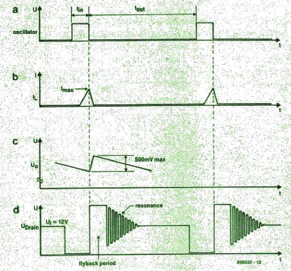 During the switch OFF period of time following the current pulse, the inductor works like a current source.
The TL497A analyzes the attenuated output voltage at pin 1 with its internal reference voltage of 1.2 V.
In case the assessed voltage is lower than the reference voltage, T1 is biased harder so that the inductor adequately stores the energy.
This repeated charge and discharge cycles triggers a certain level of ripple voltage across the output capacitors (Fig.
3c).
The feedback option allows adjusting of the oscillator frequency to ensure a the best possible compensation of voltage deficits caused by the load current.
The timing pulse diagram in Fig.
3d reveals substantial movement of the drain voltage because of the relatively high Q (quality) factor of the inductor.
Even though the stray ripple oscillations usually do not impact the regular functioning of this DC to DC power converter, these could be suppressed using a parallel 1 k resistor across the inductor.
During the switch OFF period of time following the current pulse, the inductor works like a current source.
The TL497A analyzes the attenuated output voltage at pin 1 with its internal reference voltage of 1.2 V.
In case the assessed voltage is lower than the reference voltage, T1 is biased harder so that the inductor adequately stores the energy.
This repeated charge and discharge cycles triggers a certain level of ripple voltage across the output capacitors (Fig.
3c).
The feedback option allows adjusting of the oscillator frequency to ensure a the best possible compensation of voltage deficits caused by the load current.
The timing pulse diagram in Fig.
3d reveals substantial movement of the drain voltage because of the relatively high Q (quality) factor of the inductor.
Even though the stray ripple oscillations usually do not impact the regular functioning of this DC to DC power converter, these could be suppressed using a parallel 1 k resistor across the inductor.
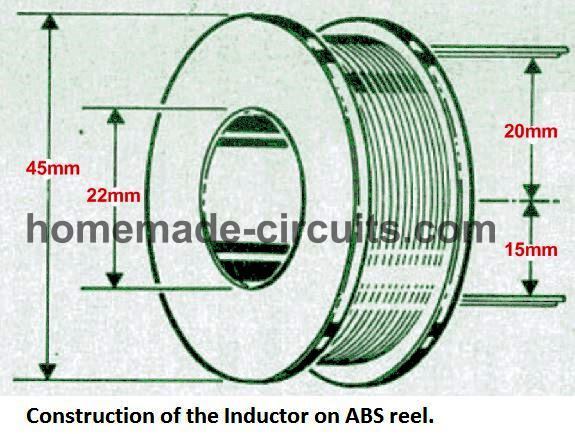 Drill a couple of 2 mm holes in the lower edge to slip the inductor wires.
One of the holes will be near the cylinder while the other on the outer circumference of the former.
It may not be useful to consider thick wire to construct the inductor, due to the the skin-effect phenomenon, that causes the shift of charge carriers along the outer surface of the wire or the skin of the wire.
This should be evaluated with regard to the magnitude of frequencies employed in the converter.
To guarantee a minimal resistance within the necessary inductance, it's advocated to work with a couple of wires of 1 mm diameter, or even 3 or 4 wires having 0.8 mm diameter in bunch.
About three 0.8 min wires will allow us to get a total dimension which may be approximately identical to two 1 mm wires, yet provides the an effective 20% higher surface area.
The inductor is tightly wound and could be sealed using an appropriate resin or epoxy based compound to control or suppress the audible noise leakage (remember that the frequency of operation is within the audible range).
Drill a couple of 2 mm holes in the lower edge to slip the inductor wires.
One of the holes will be near the cylinder while the other on the outer circumference of the former.
It may not be useful to consider thick wire to construct the inductor, due to the the skin-effect phenomenon, that causes the shift of charge carriers along the outer surface of the wire or the skin of the wire.
This should be evaluated with regard to the magnitude of frequencies employed in the converter.
To guarantee a minimal resistance within the necessary inductance, it's advocated to work with a couple of wires of 1 mm diameter, or even 3 or 4 wires having 0.8 mm diameter in bunch.
About three 0.8 min wires will allow us to get a total dimension which may be approximately identical to two 1 mm wires, yet provides the an effective 20% higher surface area.
The inductor is tightly wound and could be sealed using an appropriate resin or epoxy based compound to control or suppress the audible noise leakage (remember that the frequency of operation is within the audible range).
 Several constructional factors needs to have some considerations.
Resistors R2 and R3 might turn quite hot and therefore should be installed at the few mm elevated above the PCB surface.
The maximum current moving by means of these resistors could reach as large as 15 A.
The power-FET will also become substantially hot, and will demand a reasonably sized heatsink and the standard mica insulating kit.
The diode may possibly work without cooling down, though it may be ideally clamped over a common heatsink used for the power FET (do remember to insulate the devices electrically).
While in usual functioning, the inductor may show fair amount of heating up.
Heavy-duty connectors and cables should be incorporated at the input and output of this converter.
The battery is guarded with a 16 A delayed action fuse introduced within the input supply line.
Beware of the fact that the fuse will not provide any form of protection to the converter during output short circuits! The circuit is rather easy to set up, and may be done in the following manner:
Adjust R1 to achieve the intended output voltage which nay range between 20 and 30 V.
The output voltage could be reduced below this, although must not be less than the input voltage.
This may be done by inserting a smaller resistor in place of R4. The highest output current can be expected to be approximately 3 A.
Several constructional factors needs to have some considerations.
Resistors R2 and R3 might turn quite hot and therefore should be installed at the few mm elevated above the PCB surface.
The maximum current moving by means of these resistors could reach as large as 15 A.
The power-FET will also become substantially hot, and will demand a reasonably sized heatsink and the standard mica insulating kit.
The diode may possibly work without cooling down, though it may be ideally clamped over a common heatsink used for the power FET (do remember to insulate the devices electrically).
While in usual functioning, the inductor may show fair amount of heating up.
Heavy-duty connectors and cables should be incorporated at the input and output of this converter.
The battery is guarded with a 16 A delayed action fuse introduced within the input supply line.
Beware of the fact that the fuse will not provide any form of protection to the converter during output short circuits! The circuit is rather easy to set up, and may be done in the following manner:
Adjust R1 to achieve the intended output voltage which nay range between 20 and 30 V.
The output voltage could be reduced below this, although must not be less than the input voltage.
This may be done by inserting a smaller resistor in place of R4. The highest output current can be expected to be approximately 3 A.
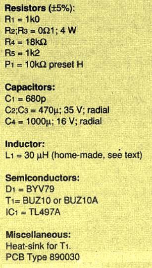
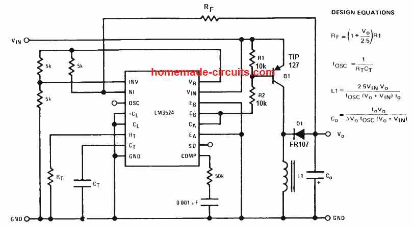 The popular IC SG3525 PWM IC could be used as high power DC 12 V to 30 V boost charger circuit application as shown above.
All the relevant circulations for determining the L1 coil details, the RF feedback resistor value and the output capacitor values are all furnished in the diagram itself.
The popular IC SG3525 PWM IC could be used as high power DC 12 V to 30 V boost charger circuit application as shown above.
All the relevant circulations for determining the L1 coil details, the RF feedback resistor value and the output capacitor values are all furnished in the diagram itself.
 They look beautiful and mimic architectural asphalt shingle roofs.
But they offer huge benefits because they can be easily installed even in smaller cutout spaces of the roof to provide sufficient solar energy for the house.
Solar shingles are as durable as regular asphalt shingles but people prefer to install any kind of solar panels over an already built-up roof.
However, they are durable and strong enough to withstand all weather conditions.
Solar shingles are more costly than regular solar panels.
They look beautiful and mimic architectural asphalt shingle roofs.
But they offer huge benefits because they can be easily installed even in smaller cutout spaces of the roof to provide sufficient solar energy for the house.
Solar shingles are as durable as regular asphalt shingles but people prefer to install any kind of solar panels over an already built-up roof.
However, they are durable and strong enough to withstand all weather conditions.
Solar shingles are more costly than regular solar panels.
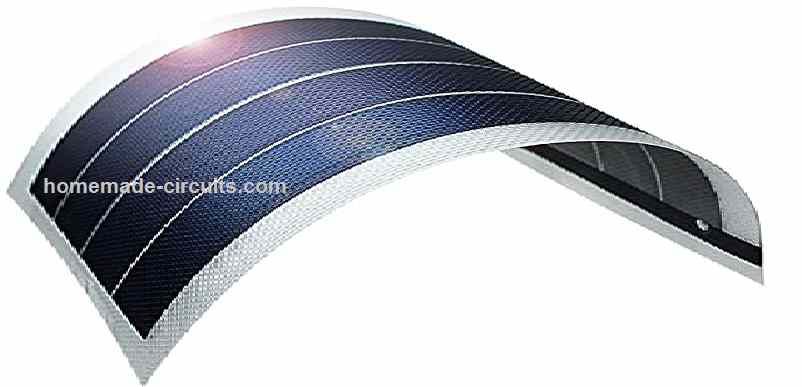 Considering that the production of thin solar film panels is less complex, hence their price is also reasonable.
Their output is 5% less than monocrystalline panel efficiency.
Normally, thin film cells deliver between 15-22% solar panel efficiency.
Thin film solar panel technology isgaining popularity as compared to more expensive types of solar panels, therefore thin film solar panels are installed on large scale projects and in record breaking solar power plants.
Thin film solar panels have relatively a shorter lifespan.
They also come with less warranty.
Considering that the production of thin solar film panels is less complex, hence their price is also reasonable.
Their output is 5% less than monocrystalline panel efficiency.
Normally, thin film cells deliver between 15-22% solar panel efficiency.
Thin film solar panel technology isgaining popularity as compared to more expensive types of solar panels, therefore thin film solar panels are installed on large scale projects and in record breaking solar power plants.
Thin film solar panels have relatively a shorter lifespan.
They also come with less warranty.
 The silicon is not grown as a single cell but as a block of crystals.
These blocks are then sliced to form thin wafers and create individual solar cells.
The current delivery of polycrystalline solar panel efficiency stands at 15-22%.
A polycrystalline solar panel is square cut and blue speckled color.
These are economical because of the process of manufacturing.
This is the reason why most people buy polycrystalline panels.
They are less heat tolerant which is the reason of the low efficiency.
They are particularly suitable for installation with high sun number score or in the areas with maximum sun days.
The silicon is not grown as a single cell but as a block of crystals.
These blocks are then sliced to form thin wafers and create individual solar cells.
The current delivery of polycrystalline solar panel efficiency stands at 15-22%.
A polycrystalline solar panel is square cut and blue speckled color.
These are economical because of the process of manufacturing.
This is the reason why most people buy polycrystalline panels.
They are less heat tolerant which is the reason of the low efficiency.
They are particularly suitable for installation with high sun number score or in the areas with maximum sun days.
 A crystal of this type of silicon is a complex process.
The rod is cut into wafers to make the solar cells.
Monocrystalline solar panels have the highest efficiency as compared to the other types of solar cells.
The efficiency of current delivery of monocrystalline solar panel stands at 22-27%.
Monocrystalline solar panel cells are more suitable for the places with a varying weather conditions like prolonged winter months.
Their efficiency is superior as compared to polycrystalline panels because they are heat tolerant and cylindrical shaped.
Monocrystalline panels are made of pure silicon.
Their colors are dark and somewhat uniform.
Monocrystalline cells cost more than polycrystalline panels but they are proving to be more economical in the long run because of their long life, more warranty and low mean time before failure (MTBF).
A crystal of this type of silicon is a complex process.
The rod is cut into wafers to make the solar cells.
Monocrystalline solar panels have the highest efficiency as compared to the other types of solar cells.
The efficiency of current delivery of monocrystalline solar panel stands at 22-27%.
Monocrystalline solar panel cells are more suitable for the places with a varying weather conditions like prolonged winter months.
Their efficiency is superior as compared to polycrystalline panels because they are heat tolerant and cylindrical shaped.
Monocrystalline panels are made of pure silicon.
Their colors are dark and somewhat uniform.
Monocrystalline cells cost more than polycrystalline panels but they are proving to be more economical in the long run because of their long life, more warranty and low mean time before failure (MTBF).
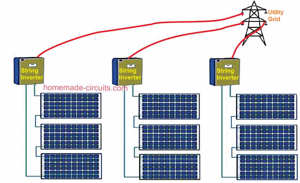
 Mix it with polyethylene glycol, which is an oily emulsifying agent, and stir the concoction carefully until a viscous cream is achieved.
 2) For the electrolyte, you can opt for iodine in ethanol, but the results may be below average compared to commercially available redox electrolyte.
3) Grab a multimeter unit and set the resistance range to find out which side of the glass piece is conductive.
2) For the electrolyte, you can opt for iodine in ethanol, but the results may be below average compared to commercially available redox electrolyte.
3) Grab a multimeter unit and set the resistance range to find out which side of the glass piece is conductive.
 4) Next, secure the glass on the table using Sellotape while placing the conductive side to face up.
 5) If you have a pipette, pull out some of the TiO2 cream or paste, and place several drops on the conductive surface of the glass.
 6) Then, using a plastic card or a different glass piece, strike the drops thoroughly.
Try getting a uniform coat by gently sliding the glass piece over the Tio2 paste.
6) Then, using a plastic card or a different glass piece, strike the drops thoroughly.
Try getting a uniform coat by gently sliding the glass piece over the Tio2 paste.
 7) Next, pull out the sellotape up around the glass free it from the table.
 8) We recommend baking the coating in an oven or over an open flame like a gas stove.
The expected temperature is around 450ˇăC.
Once it is set, arrange the support screen just by a few centimetres above the burner flame and position the glass piece with TiO2 coating on top of it.
9) The titanium oxide layer will change its color to brown at the beginning of the baking procedure because of its organic content.
But you have to ensure the color of TiO2 changes to white during the end of the process.
8) We recommend baking the coating in an oven or over an open flame like a gas stove.
The expected temperature is around 450ˇăC.
Once it is set, arrange the support screen just by a few centimetres above the burner flame and position the glass piece with TiO2 coating on top of it.
9) The titanium oxide layer will change its color to brown at the beginning of the baking procedure because of its organic content.
But you have to ensure the color of TiO2 changes to white during the end of the process.
 10) We strongly advise allowing proper cooling time for the glass otherwise thereˇŻs a chance of it shattering.
A tip is to slide the glass to a cooler area (usually near the edge) and not hastily displace it from the hot screen.
11) It is time to prepare the fruit tea with boiling water.
In our experiment, we used less water and more tea bags.
Pour the brewed fruit tea solution into a large bowl.
If you donˇŻt have fruit tea bags, you may go with red beet juice, raspberry juice or even red ink.
10) We strongly advise allowing proper cooling time for the glass otherwise thereˇŻs a chance of it shattering.
A tip is to slide the glass to a cooler area (usually near the edge) and not hastily displace it from the hot screen.
11) It is time to prepare the fruit tea with boiling water.
In our experiment, we used less water and more tea bags.
Pour the brewed fruit tea solution into a large bowl.
If you donˇŻt have fruit tea bags, you may go with red beet juice, raspberry juice or even red ink.
 12) Once the glass piece has achieved around room temperature, you may carefully slide it in the bowl and allow it to soak for several minutes.
 13) As the soaking process undergoes, you can start to cover the conductive side of a second glass piece with a lot of graphite which is obtainable from a lead pencil.
This coating will function as a catalyst for transporting electrons to the electrolyte from the electrode.
13) As the soaking process undergoes, you can start to cover the conductive side of a second glass piece with a lot of graphite which is obtainable from a lead pencil.
This coating will function as a catalyst for transporting electrons to the electrolyte from the electrode.
 14) Then, take out the conductive glass piece from the tea bath.
The titanium oxide layer will have absorbed the colour of the tea (refer to the centre of the picture).
After that, rinse the glass with clean water or ethanol and use a hairdryer to get rid of every drop of water.
14) Then, take out the conductive glass piece from the tea bath.
The titanium oxide layer will have absorbed the colour of the tea (refer to the centre of the picture).
After that, rinse the glass with clean water or ethanol and use a hairdryer to get rid of every drop of water.
 15) Next, arrange the two glass pieces together with the conductive surfaces facing one another and the ends offset.
You must take great care that both the glasses donˇŻt slide off as it may cause the TiO2 to be rubbed off.
15) Next, arrange the two glass pieces together with the conductive surfaces facing one another and the ends offset.
You must take great care that both the glasses donˇŻt slide off as it may cause the TiO2 to be rubbed off.
 16) After this, the glass pieces can be held together using paper clips (slightly modified or using normal Sellotape wrapped around them.
 17) Now, add the electrolyte between the two glass pieces.
It is recommended that you place a few drops of electrolyte on each side of the glass pieces and they will be drawn between the glasses due to capillary action.
17) Now, add the electrolyte between the two glass pieces.
It is recommended that you place a few drops of electrolyte on each side of the glass pieces and they will be drawn between the glasses due to capillary action.
 18) That's it, your fruit juice based dye-sensitized solar cell is now ready for testing.
Using the multimeter you can measure the voltage (around 0.4 V) and current (about 1 mA).
Because of the lighting of the studio, the results will vary a little.
Furthermore, you can use several crocodile clips to extend more cells in series.
18) That's it, your fruit juice based dye-sensitized solar cell is now ready for testing.
Using the multimeter you can measure the voltage (around 0.4 V) and current (about 1 mA).
Because of the lighting of the studio, the results will vary a little.
Furthermore, you can use several crocodile clips to extend more cells in series.
 We will disregard the step of sealing the glass pieces, as done with industrialized dye-sensitized solar cells.
This permits us to utilize the pieces of glass again and in that case, all you need to do is separate them and thoroughly wash their surfaces with water and gently scrub them.
Because completely removing the graphite coating is not possible, so we advise utilizing the counter-electrode glass again for the exact purpose in future experiments.
Image courtesy: youtube.com/watch?v=Jw3qCLOXmi0
We will disregard the step of sealing the glass pieces, as done with industrialized dye-sensitized solar cells.
This permits us to utilize the pieces of glass again and in that case, all you need to do is separate them and thoroughly wash their surfaces with water and gently scrub them.
Because completely removing the graphite coating is not possible, so we advise utilizing the counter-electrode glass again for the exact purpose in future experiments.
Image courtesy: youtube.com/watch?v=Jw3qCLOXmi0
 The proposed solar charge control for 100 Ah battery monitors the battery voltage and regulates the conduction level of transistor T1.
The bigger the battery voltage, the higher will be the current passing via T1. As a result, the voltage drop around R19 becomes higher.
This voltage across R19 becomes the gate switching voltage for MOSFET T2, which causes the MOSFET to switch harder, dropping its drain-to-source resistance.
Due to this the solar panel gets loaded more heavily which dissipates the excess current through the R13 and T2.
Schottky diode D7 protects the battery from accidental reversal of the + and - terminals of the solar panel.
This diode additionally stops flow of current from the battery into the solar panel in the event the panel voltage falls under the battery voltage.
The proposed solar charge control for 100 Ah battery monitors the battery voltage and regulates the conduction level of transistor T1.
The bigger the battery voltage, the higher will be the current passing via T1. As a result, the voltage drop around R19 becomes higher.
This voltage across R19 becomes the gate switching voltage for MOSFET T2, which causes the MOSFET to switch harder, dropping its drain-to-source resistance.
Due to this the solar panel gets loaded more heavily which dissipates the excess current through the R13 and T2.
Schottky diode D7 protects the battery from accidental reversal of the + and - terminals of the solar panel.
This diode additionally stops flow of current from the battery into the solar panel in the event the panel voltage falls under the battery voltage.
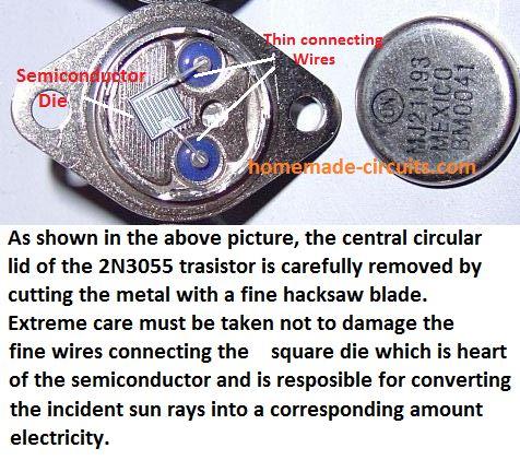
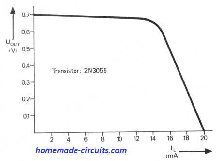
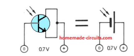 This may not be possible if the transistor is already faulty.
This is because a damaged transistor may have a faulty junction which may be short-circuited, causing a short at the output of the solar cell.
This may not be possible if the transistor is already faulty.
This is because a damaged transistor may have a faulty junction which may be short-circuited, causing a short at the output of the solar cell.
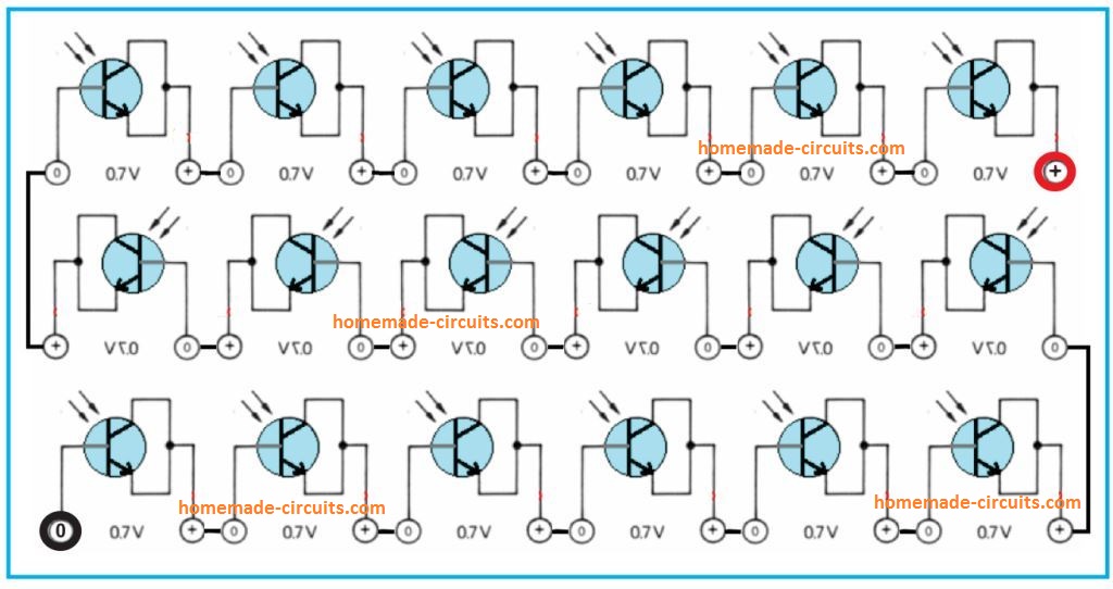 Warning: Please do not use the outdated Germanium power transistors, because these types may possibly include extremely toxic ingredients.
On the other hand, a leading semiconductor producer have ascertained that the more contemporary silicon devices, including the 2N3055, are absolutely safe in this regard.
Warning: Please do not use the outdated Germanium power transistors, because these types may possibly include extremely toxic ingredients.
On the other hand, a leading semiconductor producer have ascertained that the more contemporary silicon devices, including the 2N3055, are absolutely safe in this regard.

 The details of the various pinout functions of the above design can be learned from the following pdf link as presented by TEXAS INSTRUMENTS
48V 3kW electric vehicle circuit technical datasheet and specifications
The details of the various pinout functions of the above design can be learned from the following pdf link as presented by TEXAS INSTRUMENTS
48V 3kW electric vehicle circuit technical datasheet and specifications
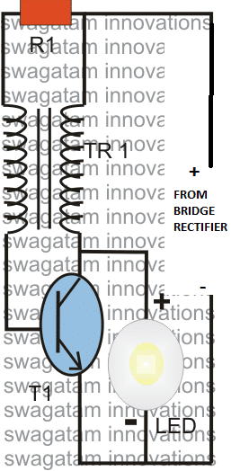 The number of turns in the above joule thief could be with a 20:20 ratio, or other proportions could also be tried for getting a preferred customized amplification.
 The IC IRS2453 enables the making of an efficient full bridge inverter circuit extremely easy.
As can be seen the output of the IC just needs 4 N channel mosfets to be integrated for implementing a full bridge inverter actions.
The IC has a built-in oscillator, so no external oscillator stage is required for initiating the shown IRS2453 IC circuit.
The Rt, Ct network associated with the IC determines the operating frequency of the inverter, and is supposed to be set at 50Hz or 60Hz depending on whether the operating voltage of the air conditioner is 220V or 120V respectively.
The IC 555 shown the left of the design is employed for generating a sine wave equivalent PWM feed for the full bridge inverter output.
The controlled PWM from the IC 555 is fed to the gates of the low side mosfets via the buffer transistor stage made through the BC547/BC557 pairs.
The above PWM feed helps the load to operate with an optimized RMS and alternating current which can be expected to be a close equivalent of the sinusoidal mains AC waveform.
The two pots associated with the IC 555 needs to be correctly adjusted until the required RMS and waveform is determined for the air conditioner.
The IC IRS2453 enables the making of an efficient full bridge inverter circuit extremely easy.
As can be seen the output of the IC just needs 4 N channel mosfets to be integrated for implementing a full bridge inverter actions.
The IC has a built-in oscillator, so no external oscillator stage is required for initiating the shown IRS2453 IC circuit.
The Rt, Ct network associated with the IC determines the operating frequency of the inverter, and is supposed to be set at 50Hz or 60Hz depending on whether the operating voltage of the air conditioner is 220V or 120V respectively.
The IC 555 shown the left of the design is employed for generating a sine wave equivalent PWM feed for the full bridge inverter output.
The controlled PWM from the IC 555 is fed to the gates of the low side mosfets via the buffer transistor stage made through the BC547/BC557 pairs.
The above PWM feed helps the load to operate with an optimized RMS and alternating current which can be expected to be a close equivalent of the sinusoidal mains AC waveform.
The two pots associated with the IC 555 needs to be correctly adjusted until the required RMS and waveform is determined for the air conditioner.

 As can be seen in the above diagram, sun rays incident on the polished concave mirror or sheet is reflected back at an inward 45 degrees to concentrate over the centrally elevated pipe, running throughout the length of the sheet.
The concentrated sun rays over this pipe can be expected to be extremely high in temperature, in the region of around 150 C, enough to force water to evaporate.
Since the intended greywater is passed into the pipe, as indicated, this water inside the pipe is bound to reach its boiling and evaporation point quite quickly releasing water vapor from the other side of the pipe, which may be collected and condensed in an overhead tank.
This collected water can be expected to be 100% clean and could be used for any desired household work, such as for washing clothes, bathing, washing utensils etc.
Many such concave mirror based greywater purifier, desalination system could be installed within a given premise for implementing the above discussed conversion of waste water to clean water through solar heat, completely free of cost, and without using any electricity.
As can be seen in the above diagram, sun rays incident on the polished concave mirror or sheet is reflected back at an inward 45 degrees to concentrate over the centrally elevated pipe, running throughout the length of the sheet.
The concentrated sun rays over this pipe can be expected to be extremely high in temperature, in the region of around 150 C, enough to force water to evaporate.
Since the intended greywater is passed into the pipe, as indicated, this water inside the pipe is bound to reach its boiling and evaporation point quite quickly releasing water vapor from the other side of the pipe, which may be collected and condensed in an overhead tank.
This collected water can be expected to be 100% clean and could be used for any desired household work, such as for washing clothes, bathing, washing utensils etc.
Many such concave mirror based greywater purifier, desalination system could be installed within a given premise for implementing the above discussed conversion of waste water to clean water through solar heat, completely free of cost, and without using any electricity.

 The water level control operation of the circuit is exactly identical to the one that's explained in this article.
As per the instructions provided in the above linked article, the motor is supposed to switch ON when the water in the tank has dropped below a particular level, which may be set by the user by installing sensor point C at the desired depth.
The water level control operation of the circuit is exactly identical to the one that's explained in this article.
As per the instructions provided in the above linked article, the motor is supposed to switch ON when the water in the tank has dropped below a particular level, which may be set by the user by installing sensor point C at the desired depth.
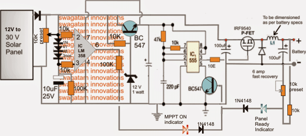
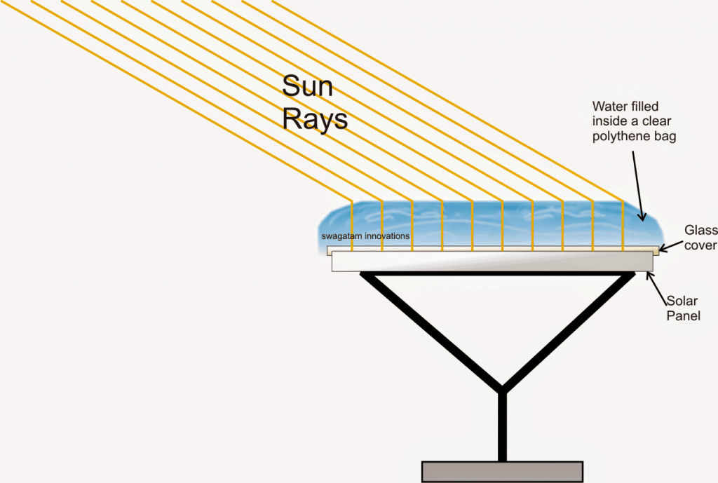 A more refined albeit costly technique may seen in the following image:

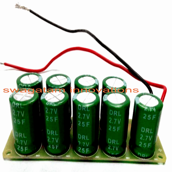 But I need to stop the reverse polarity that always occur whenever I'm charging it with an hand crank 24Vdc generator.
Please Swag, what exact Diode should I use? How do I get the positive and Negative terminals of the Diode in order to solder correctly the Diode to the Super-cap Module?
Thank you in advance.
P.S: please if possible, give me a pictorial guide.
Thank you a Million times.
But I need to stop the reverse polarity that always occur whenever I'm charging it with an hand crank 24Vdc generator.
Please Swag, what exact Diode should I use? How do I get the positive and Negative terminals of the Diode in order to solder correctly the Diode to the Super-cap Module?
Thank you in advance.
P.S: please if possible, give me a pictorial guide.
Thank you a Million times.
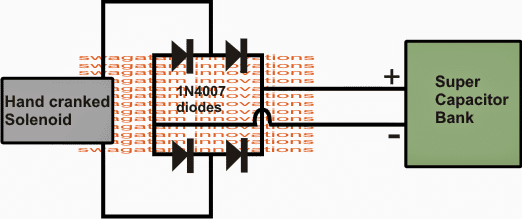
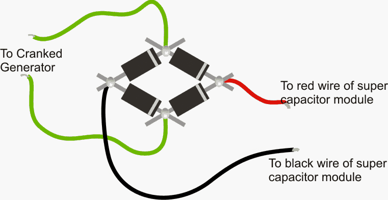 The reverse current will matter only in case if the red/black wires are reversed while connecting with the super capacitor....
the capacitors will get damaged if the current in this condition exceeds 1 amp.
The reverse current will matter only in case if the red/black wires are reversed while connecting with the super capacitor....
the capacitors will get damaged if the current in this condition exceeds 1 amp.

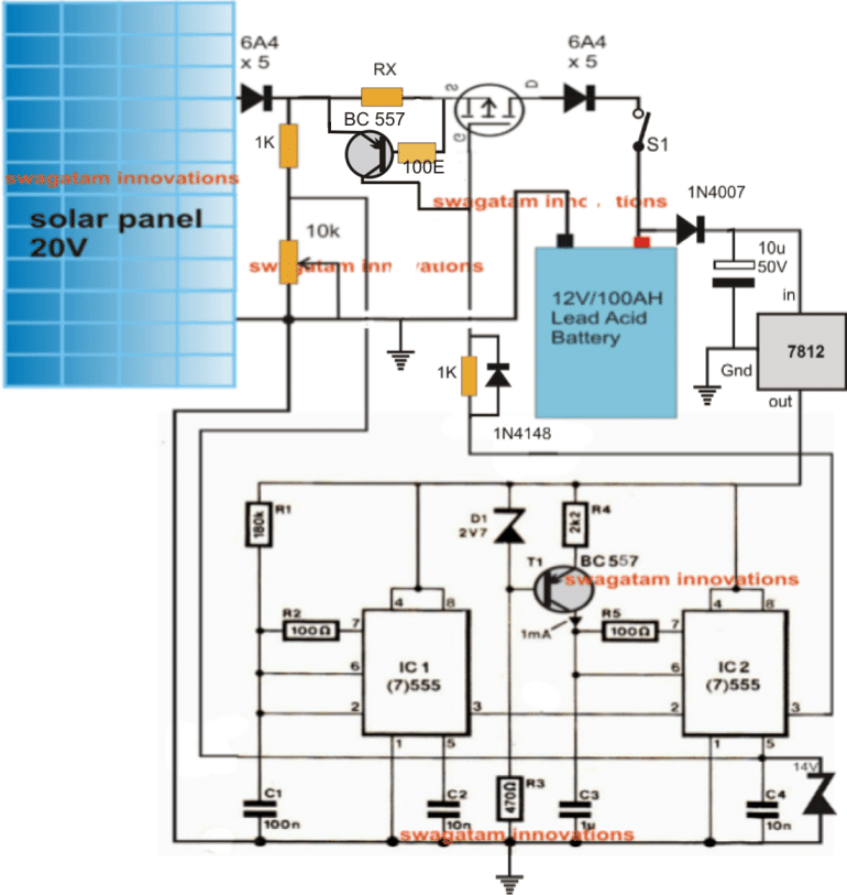 A crude but simpler version of the above explained design may be built as suggested by Mr.
Dhyaksa using pin2 and pin6 threshold detection of the IC555, the entire diagram may be witnessed below:
A crude but simpler version of the above explained design may be built as suggested by Mr.
Dhyaksa using pin2 and pin6 threshold detection of the IC555, the entire diagram may be witnessed below:
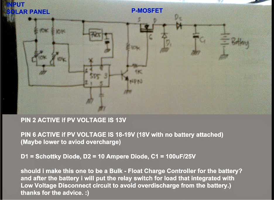
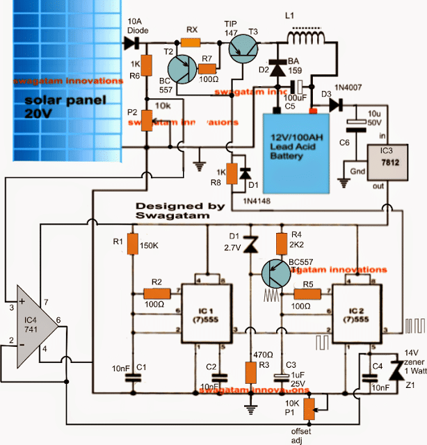 As you can see in the above diagram, the basic diagram is identical to the earlier self optimizing solar charger circuit, except the inclusion of IC4 which is configured as a voltage follower and is replaced in place of the BC547 emitter follower stage.
This is done in order to provide a better response for the IC2 pin#5 control pinout from the panel.
As you can see in the above diagram, the basic diagram is identical to the earlier self optimizing solar charger circuit, except the inclusion of IC4 which is configured as a voltage follower and is replaced in place of the BC547 emitter follower stage.
This is done in order to provide a better response for the IC2 pin#5 control pinout from the panel.
 When sunshine drops, voltage of the panel also drops and now we cannot afford to draw heavy current from the panel because that would bring down the voltage below 12V which might entirely stop the charging process.


 As per the request, the above circuit must be powered from a battery, charged from a solar charger controller circuit.
I have explained many solar charger controller circuits in this blog, the LAST CIRCUIT given in the article may be used for the present application.
As per the request, the above circuit must be powered from a battery, charged from a solar charger controller circuit.
I have explained many solar charger controller circuits in this blog, the LAST CIRCUIT given in the article may be used for the present application.
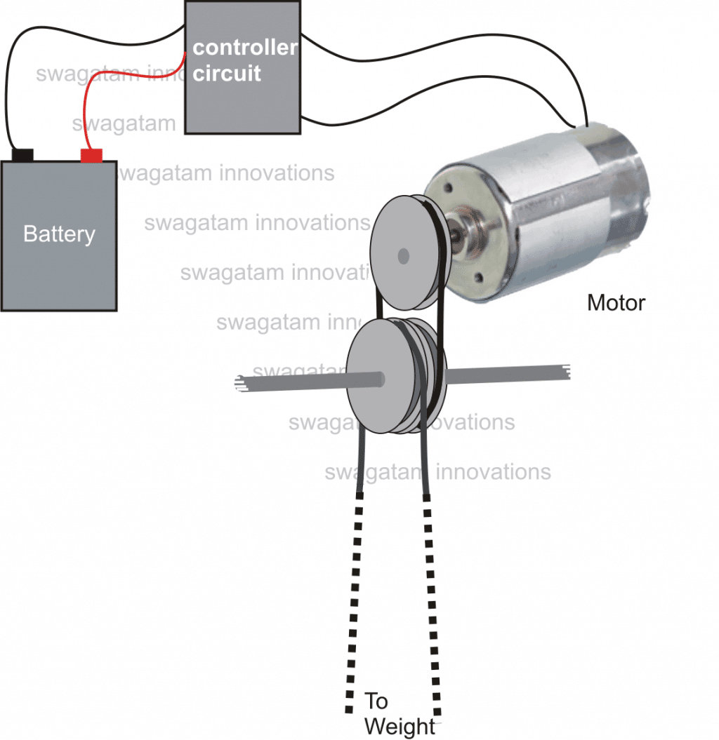 A simple charger/controller is shown below, which can be employed for this application too.
The circuit utilizes the well known IC LM338.
The "push-pull" voltage from the motor, or the alternating voltage from the motor is first rectified by the four diodes, filtered by the capacitor and regulated to the desired battery voltage by the IC LM338 circuit.
A simple charger/controller is shown below, which can be employed for this application too.
The circuit utilizes the well known IC LM338.
The "push-pull" voltage from the motor, or the alternating voltage from the motor is first rectified by the four diodes, filtered by the capacitor and regulated to the desired battery voltage by the IC LM338 circuit.
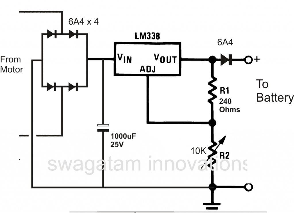
 Please use 1N5408 diodes instead of 1N5402, mistakenly shown in the above diagram.
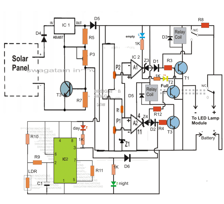 The above design can be much simplified by eliminating the IC 555 stage and by connecting the day time relay cut OFF transistor directly with the solar panel positive, as shown below:

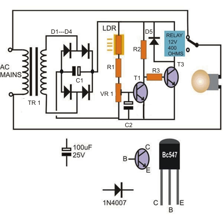
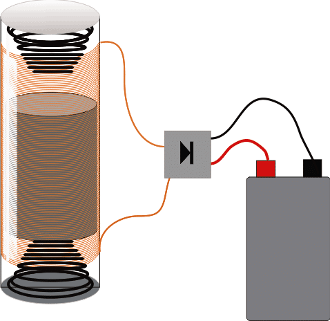
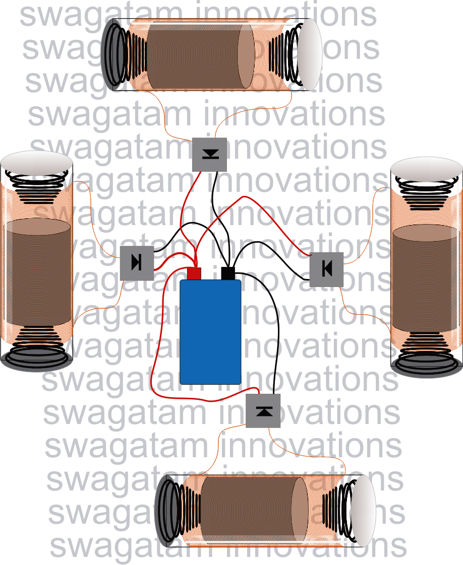 The tube encloses a cylindrical magnet having a north (N) and south (S) pole over its ends.
The magnetdiameterand the internal tube diameter arechosensuch that the magnet just slides inside the tube freelywithoutwobbling sideways much.
The tube top and bottomportionsare sealed with lidshavinga low tension spring fixed inward for facilitating abouncyeffect to the jumping magnet.
Four such assemblies are positioned perpendicular to each other inside the football for keeping a uniformalignmentto the ball and its dynamics.
The coil wire terminals from each assembly is connected to individual bridge rectifiers and the outputs from all the bridge rectifiers are appropriately connected to a correctly rated battery, either a Li-Ion or Ni-Cd.
The whole assembly along with the battery is then neatly framed and securely fixed inside a football.
The tube encloses a cylindrical magnet having a north (N) and south (S) pole over its ends.
The magnetdiameterand the internal tube diameter arechosensuch that the magnet just slides inside the tube freelywithoutwobbling sideways much.
The tube top and bottomportionsare sealed with lidshavinga low tension spring fixed inward for facilitating abouncyeffect to the jumping magnet.
Four such assemblies are positioned perpendicular to each other inside the football for keeping a uniformalignmentto the ball and its dynamics.
The coil wire terminals from each assembly is connected to individual bridge rectifiers and the outputs from all the bridge rectifiers are appropriately connected to a correctly rated battery, either a Li-Ion or Ni-Cd.
The whole assembly along with the battery is then neatly framed and securely fixed inside a football.
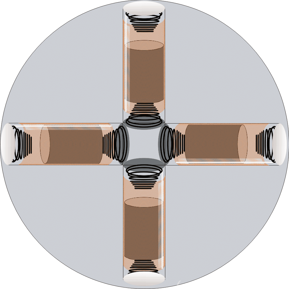
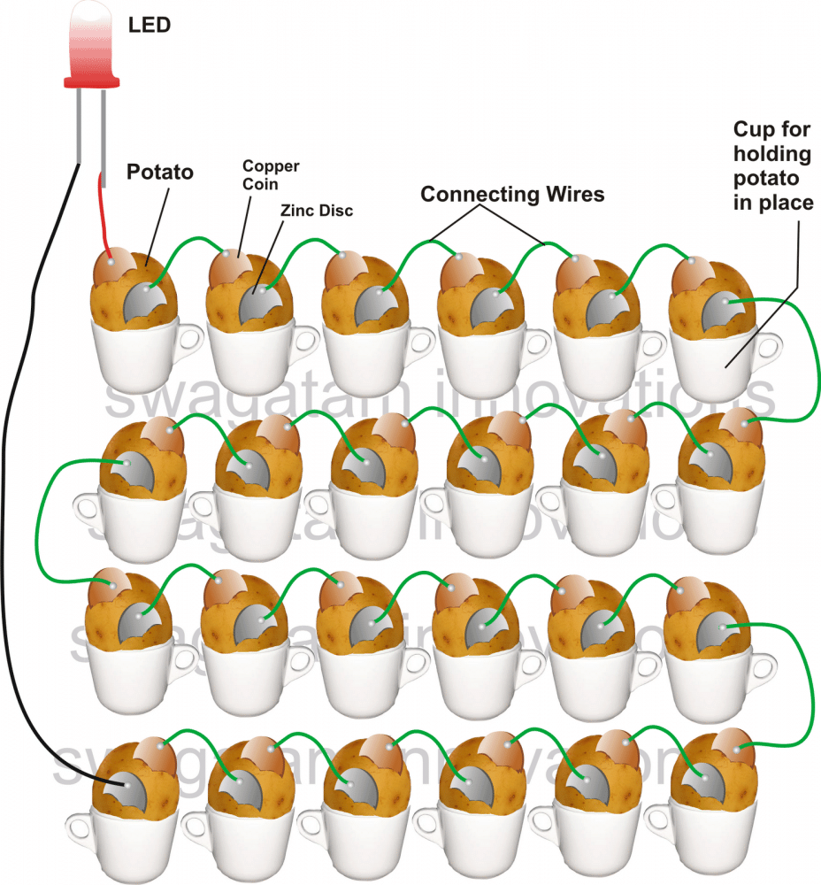
 Once the sphere is filled with water, it behaves like a big, solid and a powerful convex lens.
In our childhood days we all have played with this amazing piece of lenses.
We have seen how it is able to focus and concentrate sun rays at one single point when placed at a particular angle under sunlight.
(Click Image to Enlarge) The created focal point is in fact a concentrated beam of the sun rays collected and deflected at a small point.
This point is very hot, and is able to produce burning effect over anything placed under it.
The above principle has been simply exploited in the present design.
Without water the sphere is ineffective and will act just like a normal glass.
The sunrays entering into it thus cannot generate much of a heat.
But the moment it is filled with water, it is transformed into a big solid convex lens having a focal point exactly at its center.
Sun rays hitting the glass sphere are instantly refracted through the entire curvature of the filled water to reach exactly at the center.
Here the rays concentrate into single hot spot.
Water at this point starts heating up instantly and the heat is gradually transferred to the whole mass of the filled water.
As the temperature rises, water molecules are converted into vapor.
The water vapor formed, rise through the ˇ°Tˇ± shaped glass tube and the reservoir tank.
The tank being relatively much cooler helps in converting the received water vapor into clean, drinkable water* (see comments) on its roof.
Water molecules accumulated on the roof of the reservoir tank slowly gather to form water drops which ultimately fall into the tank and pure water is thus collected inside the tank.
This water is absolutely pure, and free from viruses, bacteria or dust particles.
The efficiency of this apparatus will decrease if the filled water is murky or muddy.
Because in such a case the focal point will be comparatively dull and wonˇŻt be able to create enough heat.
The above method should have certainly made you understand regarding how to desalinate sea water simply and efficiently.
UPDATE:
Th above design looks quite inefficient since the apparatus is cumbersome and difficult to implement for large scale desalination process.
A much better and simpler design can be seen below.
The diagram is self explanatory:
Once the sphere is filled with water, it behaves like a big, solid and a powerful convex lens.
In our childhood days we all have played with this amazing piece of lenses.
We have seen how it is able to focus and concentrate sun rays at one single point when placed at a particular angle under sunlight.
(Click Image to Enlarge) The created focal point is in fact a concentrated beam of the sun rays collected and deflected at a small point.
This point is very hot, and is able to produce burning effect over anything placed under it.
The above principle has been simply exploited in the present design.
Without water the sphere is ineffective and will act just like a normal glass.
The sunrays entering into it thus cannot generate much of a heat.
But the moment it is filled with water, it is transformed into a big solid convex lens having a focal point exactly at its center.
Sun rays hitting the glass sphere are instantly refracted through the entire curvature of the filled water to reach exactly at the center.
Here the rays concentrate into single hot spot.
Water at this point starts heating up instantly and the heat is gradually transferred to the whole mass of the filled water.
As the temperature rises, water molecules are converted into vapor.
The water vapor formed, rise through the ˇ°Tˇ± shaped glass tube and the reservoir tank.
The tank being relatively much cooler helps in converting the received water vapor into clean, drinkable water* (see comments) on its roof.
Water molecules accumulated on the roof of the reservoir tank slowly gather to form water drops which ultimately fall into the tank and pure water is thus collected inside the tank.
This water is absolutely pure, and free from viruses, bacteria or dust particles.
The efficiency of this apparatus will decrease if the filled water is murky or muddy.
Because in such a case the focal point will be comparatively dull and wonˇŻt be able to create enough heat.
The above method should have certainly made you understand regarding how to desalinate sea water simply and efficiently.
UPDATE:
Th above design looks quite inefficient since the apparatus is cumbersome and difficult to implement for large scale desalination process.
A much better and simpler design can be seen below.
The diagram is self explanatory:

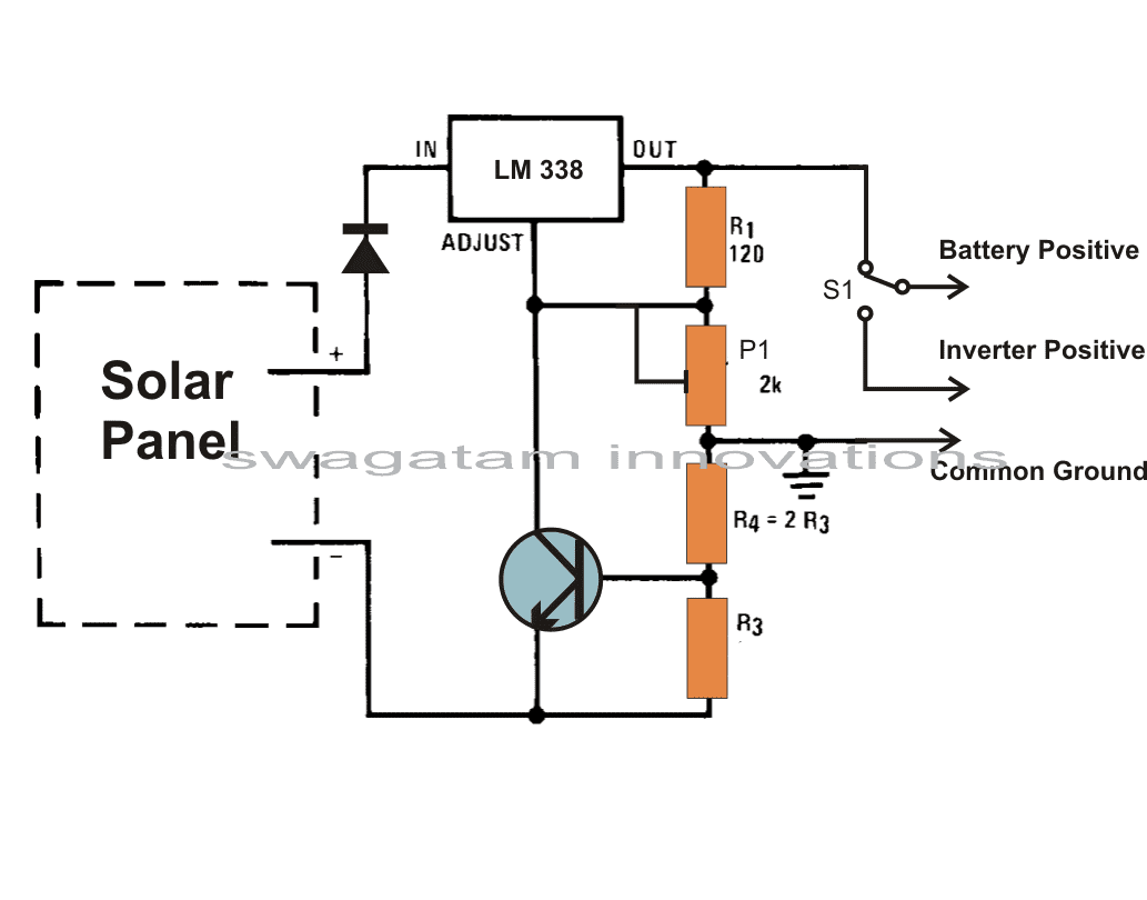 NOTE: PLEASE REMOVE R4, AS IT HAS NO REAL IMPORTANCE.
YOU CAN REPLACE IT WITH A WIRE LINK.
Track side PCB Design (R4, Diode and S1 not included...R4 is actually not important and may be replaced with a jumper wire.
NOTE: PLEASE REMOVE R4, AS IT HAS NO REAL IMPORTANCE.
YOU CAN REPLACE IT WITH A WIRE LINK.
Track side PCB Design (R4, Diode and S1 not included...R4 is actually not important and may be replaced with a jumper wire.
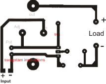
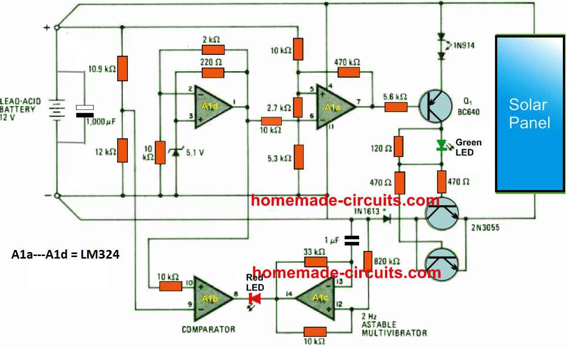 As opposed to a number of other shunt regulators that will redirect current through a resistor once the battery is completely charged, this circuit disconnects the charging supply from the battery eliminating the need of bulky shunt resistors.
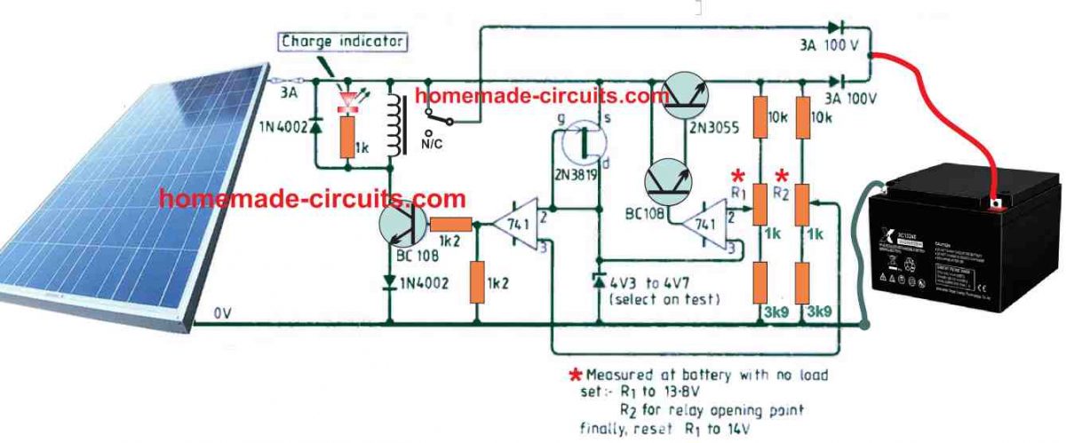 This set up can be great so long as the battery does not get overcharged, since a 12V battery can easily become overcharged to above 1V5, in case the charging supply is not controlled.
Voltage drop induced through a series pass BJT, typically is approximately 1.2V, which appears to be way too high for nearly all solar panels to operate effectively.
Both the above flaws are effectively removed in this simple solar regulator circuit.
Here, energy from the solar panel is supplied to the battery via a relay and rectifier diode.
This set up can be great so long as the battery does not get overcharged, since a 12V battery can easily become overcharged to above 1V5, in case the charging supply is not controlled.
Voltage drop induced through a series pass BJT, typically is approximately 1.2V, which appears to be way too high for nearly all solar panels to operate effectively.
Both the above flaws are effectively removed in this simple solar regulator circuit.
Here, energy from the solar panel is supplied to the battery via a relay and rectifier diode.
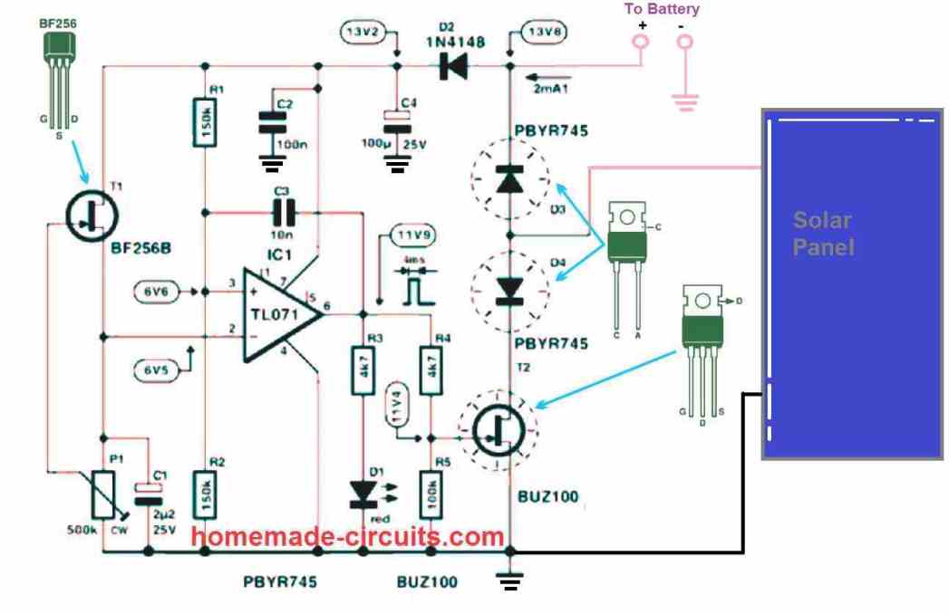 The shunt type solar panel regulator circuit shown above can be understood with the following points:
The op amp TL071 is configured like a comparator.
The FET BF256 along with the 500k preset P1 forms a constant current and constant voltage reference generator for the inverting input of the op amp.
THe pin3 which is the non-inverting input for the op amp is held with varying voltage source depending on the level of the battery terminal voltage, therefore this pin3 works like the over charge sensing input of the compartaor op amp.
The preset P1 at pin2 of the IC is adjusted in such a way that the potential at pin3 input of the IC is just higher the pin2 as soon as the battery reaches the full charge level.
While the battery level is below the full charge value, the potential at the pin3 is lower than the pin2 which keeps the output of the op amp to zero logic, and the FET T2 BUZ100 remains switched OFF.
However, as soon as the battery reaches the full charge level, the pin3 potential now increase above the pin2 value, which causes the output of the op amp to change state to a high output.
This immediately switches ON the FET T1, which shunts the solar panel voltage to ground, thereby preventing any further charging of the battery.
While the solar panel voltage is being shunted by the FET T1 via the diode D4, these two devices can get substantially hot, since the whole solar panel power gets grounded by these two devices.
The diode D3 ensures that once the battery is charged, it never gets discharged through the solar panel, especially during the night time.
The LED D1 indicates when the battery is fully charged and cut off, as it gets switched ON.
Parts List
The shunt type solar panel regulator circuit shown above can be understood with the following points:
The op amp TL071 is configured like a comparator.
The FET BF256 along with the 500k preset P1 forms a constant current and constant voltage reference generator for the inverting input of the op amp.
THe pin3 which is the non-inverting input for the op amp is held with varying voltage source depending on the level of the battery terminal voltage, therefore this pin3 works like the over charge sensing input of the compartaor op amp.
The preset P1 at pin2 of the IC is adjusted in such a way that the potential at pin3 input of the IC is just higher the pin2 as soon as the battery reaches the full charge level.
While the battery level is below the full charge value, the potential at the pin3 is lower than the pin2 which keeps the output of the op amp to zero logic, and the FET T2 BUZ100 remains switched OFF.
However, as soon as the battery reaches the full charge level, the pin3 potential now increase above the pin2 value, which causes the output of the op amp to change state to a high output.
This immediately switches ON the FET T1, which shunts the solar panel voltage to ground, thereby preventing any further charging of the battery.
While the solar panel voltage is being shunted by the FET T1 via the diode D4, these two devices can get substantially hot, since the whole solar panel power gets grounded by these two devices.
The diode D3 ensures that once the battery is charged, it never gets discharged through the solar panel, especially during the night time.
The LED D1 indicates when the battery is fully charged and cut off, as it gets switched ON.
Parts List
 After youˇŻve procured all the above components, the fixing of the units can be started with the following steps:
Install the panels over the roof of your house, such that it faces straight into the sky.
This orientation ensures that the panel remains exposed to the sun light during most of the time between day break and dusk.
The above position should provide a maximum of 24 volts when the sun light is perfectly incident over the panel and around 12 volts during twilight periods.
You can check the output voltage from the panel, using a multitester (DC volt range) when thereˇŻs sufficient daylight over the panels.
Next comes the testing of the battery charger/regulator unit, it can be done by temporarily connecting its inputs to the solar output voltage (around 15 to 20 volts).
Now checking the output from the regulator must read around 14 volts, this confirms the correct functioning of the unit.
The inverter may normally need no testing as it may be done prior to buying it from the dealer.
Now itˇŻs time to integrate the inverter with the regulator, again thatˇŻs very simple.
Just connect the output terminals of the regulator/charger to the battery input of the inverter.
Also plug-in the inverter to the mains input line of your house electrical.
You might want to take the help of a professional electrician only for this part of the connection.
Position the charger and the inverter assembly in one corner of the house, such that they are safely placed away from heat, water and human interventions.
The battery which is the main power storage component may now be brought into the scene and joined with the regulatorˇŻs relevant terminals (indicated as (+)(-) bat).
Finally itˇŻs the moment when we connected the solar panel with the above positioned units.
Connect wires of required length to the solar panel terminals and neatly escort them to the house interior so that they can be connected to the charger relevant terminals (written as +IN and ¨CIN).
With the above configuration done correctly as discussed and the sunlight at full throttle, your battery will start getting charged.
The regulator will monitor the charge and switches it OFF and ON as per the situation.
Assuming the battery in the charged condition initially, would require 6 hours of charging from the panels after which the inverter may be turned ON for receiving the desired AC power, preferable it must be done when itˇŻs relatively dark inside the house.
Alternatively a diesel operated car alternator may be incorporated for feeding the inverter through another regulator assembly and a change over switch.
This action will ensure an AC power to the house 24-7.
After youˇŻve procured all the above components, the fixing of the units can be started with the following steps:
Install the panels over the roof of your house, such that it faces straight into the sky.
This orientation ensures that the panel remains exposed to the sun light during most of the time between day break and dusk.
The above position should provide a maximum of 24 volts when the sun light is perfectly incident over the panel and around 12 volts during twilight periods.
You can check the output voltage from the panel, using a multitester (DC volt range) when thereˇŻs sufficient daylight over the panels.
Next comes the testing of the battery charger/regulator unit, it can be done by temporarily connecting its inputs to the solar output voltage (around 15 to 20 volts).
Now checking the output from the regulator must read around 14 volts, this confirms the correct functioning of the unit.
The inverter may normally need no testing as it may be done prior to buying it from the dealer.
Now itˇŻs time to integrate the inverter with the regulator, again thatˇŻs very simple.
Just connect the output terminals of the regulator/charger to the battery input of the inverter.
Also plug-in the inverter to the mains input line of your house electrical.
You might want to take the help of a professional electrician only for this part of the connection.
Position the charger and the inverter assembly in one corner of the house, such that they are safely placed away from heat, water and human interventions.
The battery which is the main power storage component may now be brought into the scene and joined with the regulatorˇŻs relevant terminals (indicated as (+)(-) bat).
Finally itˇŻs the moment when we connected the solar panel with the above positioned units.
Connect wires of required length to the solar panel terminals and neatly escort them to the house interior so that they can be connected to the charger relevant terminals (written as +IN and ¨CIN).
With the above configuration done correctly as discussed and the sunlight at full throttle, your battery will start getting charged.
The regulator will monitor the charge and switches it OFF and ON as per the situation.
Assuming the battery in the charged condition initially, would require 6 hours of charging from the panels after which the inverter may be turned ON for receiving the desired AC power, preferable it must be done when itˇŻs relatively dark inside the house.
Alternatively a diesel operated car alternator may be incorporated for feeding the inverter through another regulator assembly and a change over switch.
This action will ensure an AC power to the house 24-7.
 The working of the circuit can be understood with the following points:
When the cellphone which is shown near the MIC is called by the owner, its ringtone noise is detected by the MIC.
This triggers the transistor T1, T2, and T3 in succession, which finally turns ON the relay.
The relay can be seen attached with a tiny 6 V water pump, which s switched ON.
It remains switched ON as long the ringtone remains active from the cellphone.
The transistorized circuit is basically a MIC amplifier circuit, which amplifies the small electrical signals from the MIC, generated due to the ringtone sound.
T1 does the job of a preamplifier, while T2 and T3 further amplifies the preamplified signal from T1, so that the current becomes sufficiently large to switch ON a relay.
The capacitor C2 determines for how long the relay can continue to remain ON after the ringtone has stopped.
R1 decides the sensitivity of the circuit to sound inputs.
If you want to ensure the MIC circuit does not get triggered due to stray external sounds, you can increase the value of R1 to 10 k or higher.
The cellphone controlled plant watering circuit is simple and cheap, but it has one drawback, it cannot send an SMS back to the owner to confirm regarding the actions, which means the owner can never know whether the water pump was actually activated or not.
Nevertheless, the transistorized circuit being small and simple is extremely reliable and it will respond impeccably to the ringtone sounds and activate the water pump relay without fail.
The working of the circuit can be understood with the following points:
When the cellphone which is shown near the MIC is called by the owner, its ringtone noise is detected by the MIC.
This triggers the transistor T1, T2, and T3 in succession, which finally turns ON the relay.
The relay can be seen attached with a tiny 6 V water pump, which s switched ON.
It remains switched ON as long the ringtone remains active from the cellphone.
The transistorized circuit is basically a MIC amplifier circuit, which amplifies the small electrical signals from the MIC, generated due to the ringtone sound.
T1 does the job of a preamplifier, while T2 and T3 further amplifies the preamplified signal from T1, so that the current becomes sufficiently large to switch ON a relay.
The capacitor C2 determines for how long the relay can continue to remain ON after the ringtone has stopped.
R1 decides the sensitivity of the circuit to sound inputs.
If you want to ensure the MIC circuit does not get triggered due to stray external sounds, you can increase the value of R1 to 10 k or higher.
The cellphone controlled plant watering circuit is simple and cheap, but it has one drawback, it cannot send an SMS back to the owner to confirm regarding the actions, which means the owner can never know whether the water pump was actually activated or not.
Nevertheless, the transistorized circuit being small and simple is extremely reliable and it will respond impeccably to the ringtone sounds and activate the water pump relay without fail.
 The delay period of the oscillator is determined by the components P1, R2, and C1. The delay determines for how long the relay remains switched OFF and at what time of the day (or night) it switches ON the water pump.
You will find that the IC has many pinouts which generate the output oscillations at different frequency rates, each being twice of the previous output pin.
Out of all the output pins, the pin#3 generates the lowest frequency, or the highest delay, or the highest ON time period outputs.
For this reason pin#3 is selected for generating the time intervals for the relay and the water pump activation.
When power is switched ON, the C2 momentarily resets the IC by supplying a short high pulse on its pin#12.
The resetting ensures that the IC timing begins from zero, with pin#3 initiating with a low output.
While the IC counts, the pin#3 remains low, which allows the transistor-relay stage to remain switched OFF.
As soon as the IC timing elapses, the pin#3 turns high and a couple of things things happen simultaneously.
The high signal enters D3 charging up C3, and it also passes through D1 to hit pin#12, which resets the IC, so that pin#3 turn instantly turns low again, and the counting begins afresh.
This process is crucial as it ensures that the delay cycles are almost identical in length, without discrepancies.
However, this short momentary pulse is enough to charge C3 fully and cause the transistor T1 to switch ON.
When T1 switches ON, the relay also switches ON, which turns ON the water pump.
The charge inside C3 ensures that T1 remains remains ON for sometime, maybe for 5 to 8 seconds, which is enough time to water a flower pot or any small plant.
If you want the relay to be switched ON for higher amount of time, you can replace T1 with a Darlington transistor, and increase the R4 value to 100K, which may increase the relay ON time to around a minute.
The delay period of the oscillator is determined by the components P1, R2, and C1. The delay determines for how long the relay remains switched OFF and at what time of the day (or night) it switches ON the water pump.
You will find that the IC has many pinouts which generate the output oscillations at different frequency rates, each being twice of the previous output pin.
Out of all the output pins, the pin#3 generates the lowest frequency, or the highest delay, or the highest ON time period outputs.
For this reason pin#3 is selected for generating the time intervals for the relay and the water pump activation.
When power is switched ON, the C2 momentarily resets the IC by supplying a short high pulse on its pin#12.
The resetting ensures that the IC timing begins from zero, with pin#3 initiating with a low output.
While the IC counts, the pin#3 remains low, which allows the transistor-relay stage to remain switched OFF.
As soon as the IC timing elapses, the pin#3 turns high and a couple of things things happen simultaneously.
The high signal enters D3 charging up C3, and it also passes through D1 to hit pin#12, which resets the IC, so that pin#3 turn instantly turns low again, and the counting begins afresh.
This process is crucial as it ensures that the delay cycles are almost identical in length, without discrepancies.
However, this short momentary pulse is enough to charge C3 fully and cause the transistor T1 to switch ON.
When T1 switches ON, the relay also switches ON, which turns ON the water pump.
The charge inside C3 ensures that T1 remains remains ON for sometime, maybe for 5 to 8 seconds, which is enough time to water a flower pot or any small plant.
If you want the relay to be switched ON for higher amount of time, you can replace T1 with a Darlington transistor, and increase the R4 value to 100K, which may increase the relay ON time to around a minute.
 The addition of the IC2 enables the design to produce reasonably longer time delays through an ordinary IC like the IC 555, since it converts the single pulse time intervals from the IC 555 into 10 times longer time intervals.
Thus, 1 second time periods from the IC 555 gets converted into 99 seconds, 10 seconds gets converted to 90 seconds, and 1 minute is scaled up to 99 minutes.
IC2 also allows the timing capacitor C1 to be relatively smaller and compact.
However, if you want the output delays many times higher than this, then IC 555 could be replaced with a more accurate timer IC like the IC 4060, for enabling bigger selectable ranges which can be 10 times higher than the proposed ranges.
The circuit has a 3 way selector switch, which can be used for setting one of 3 timing ranges.
Each timing range has its own separate variable resistor or potentiometer which can be calibrated to further to breakdown each range into smaller time interval divisions.
The addition of the IC2 enables the design to produce reasonably longer time delays through an ordinary IC like the IC 555, since it converts the single pulse time intervals from the IC 555 into 10 times longer time intervals.
Thus, 1 second time periods from the IC 555 gets converted into 99 seconds, 10 seconds gets converted to 90 seconds, and 1 minute is scaled up to 99 minutes.
IC2 also allows the timing capacitor C1 to be relatively smaller and compact.
However, if you want the output delays many times higher than this, then IC 555 could be replaced with a more accurate timer IC like the IC 4060, for enabling bigger selectable ranges which can be 10 times higher than the proposed ranges.
The circuit has a 3 way selector switch, which can be used for setting one of 3 timing ranges.
Each timing range has its own separate variable resistor or potentiometer which can be calibrated to further to breakdown each range into smaller time interval divisions.

 Warning: The Circuit is Not Isolated from Mains AC, and therefore is extremely dangerous to touch in an uncovered, switched ON position.
Proceed with extreme caution while testing this circuit.
Warning: The Circuit is Not Isolated from Mains AC, and therefore is extremely dangerous to touch in an uncovered, switched ON position.
Proceed with extreme caution while testing this circuit.
 UVC radiation having wavelength between 100 nm and 280 nm has the ability to burst the DNA of bacteria, viruses and spores causing an immediate deactivation of their cells.
It can easily rupture the RNA protein of any virus, even the Novel Coronavirus, and therefore could be effectively applied for sanitizing purposes against novel Coronavirus pandemic.
UV radiation may be applied for several sterilization applications in water and air treatment, however mainly it works the best for disinfection process which eliminates all forms non-chemical based micro-organisms.
However, since human skin also contains DNA material, can be susceptible to UV radiation causing burns, skin damage and skin cancer.
Therefore, UV rays of any level must be strictly avoided from human skin contact.
The disinfection process must be implemented only inside a well shielded container with the intended materials stuffed inside, which need to be disinfected.
Must read: UVC disinfecting lamps which can inactivate Coronavirus and yet be safe for humans.
UVC radiation having wavelength between 100 nm and 280 nm has the ability to burst the DNA of bacteria, viruses and spores causing an immediate deactivation of their cells.
It can easily rupture the RNA protein of any virus, even the Novel Coronavirus, and therefore could be effectively applied for sanitizing purposes against novel Coronavirus pandemic.
UV radiation may be applied for several sterilization applications in water and air treatment, however mainly it works the best for disinfection process which eliminates all forms non-chemical based micro-organisms.
However, since human skin also contains DNA material, can be susceptible to UV radiation causing burns, skin damage and skin cancer.
Therefore, UV rays of any level must be strictly avoided from human skin contact.
The disinfection process must be implemented only inside a well shielded container with the intended materials stuffed inside, which need to be disinfected.
Must read: UVC disinfecting lamps which can inactivate Coronavirus and yet be safe for humans.
 A popular, effective and cheap UV-C bulb is the 3 watt UV germicidal bulb, as shown below, having the following specifications
 Item Type: Ultraviolet UV-C Lamps
Voltage: 85-265V
is_customized: Yes
Certification: CE, LVD, RoHS
Temperature: Warm White (2700-3500K)
Features: Germicidal
Average Life (hrs): 1000
Warranty: 1000 hours
Base Type: E17
Wattage: 3W
Item Type: Ultraviolet UV-C Lamps
Voltage: 85-265V
is_customized: Yes
Certification: CE, LVD, RoHS
Temperature: Warm White (2700-3500K)
Features: Germicidal
Average Life (hrs): 1000
Warranty: 1000 hours
Base Type: E17
Wattage: 3W
 Among all other materials, our cellphone may be the most vulnerable to Coronavirus infection or harboring, therefore we will discuss a method of using UV-C based enclosure that could be used for disinfecting a cellphone, or other similar objects from all possible microbes.

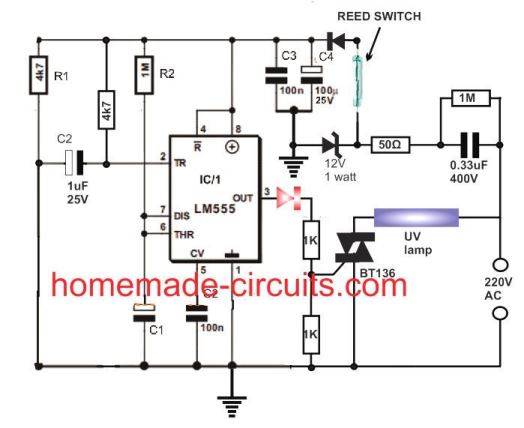 The circuit working can be understood with the help of the following points.
The IC 555 is wired as a standard monostable multivibrator, powered through a stabilized transformerless power supply circuit, comprising of C3, C4, 0.33uF, and the 12V zener diode.
As soon the circuit is powered from the AC mains, the 12V DC across the monostable instantly triggers the circuit via the 1uF capacitor connected pin2 of the IC.
The capacitor momentarily grounds the pin2 of the IC activating its output pin3 with a positive supply.
The positive supply at pin3 activates the triac and the UV lamp.
The monostable now begins counting, and depending on the values of the C1, and R2, the pin3 and the triac remain switched ON for a stipulated period of time.
When the time elapses, the pin3 becomes zero, switching off the triac and the UV lamp.
We can also see a reed relay connected in series with the positive line of the input supply.
This reed relay is coupled with a magnet, associated with door mechanism of the UV box cabinet.
As long as the door is in the open position the magnet is pulled away from the reed relay, causing its contacts to remain open, and the monostable to be powered off.
When the door is closed, the magnet is pulled close to the reed relay, forcing its contacts to close, and switch ON the supply for the monostable.
The monostable now switches ON, causing the timer and the UV lamp to activate for the intended actions.
The circuit working can be understood with the help of the following points.
The IC 555 is wired as a standard monostable multivibrator, powered through a stabilized transformerless power supply circuit, comprising of C3, C4, 0.33uF, and the 12V zener diode.
As soon the circuit is powered from the AC mains, the 12V DC across the monostable instantly triggers the circuit via the 1uF capacitor connected pin2 of the IC.
The capacitor momentarily grounds the pin2 of the IC activating its output pin3 with a positive supply.
The positive supply at pin3 activates the triac and the UV lamp.
The monostable now begins counting, and depending on the values of the C1, and R2, the pin3 and the triac remain switched ON for a stipulated period of time.
When the time elapses, the pin3 becomes zero, switching off the triac and the UV lamp.
We can also see a reed relay connected in series with the positive line of the input supply.
This reed relay is coupled with a magnet, associated with door mechanism of the UV box cabinet.
As long as the door is in the open position the magnet is pulled away from the reed relay, causing its contacts to remain open, and the monostable to be powered off.
When the door is closed, the magnet is pulled close to the reed relay, forcing its contacts to close, and switch ON the supply for the monostable.
The monostable now switches ON, causing the timer and the UV lamp to activate for the intended actions.
 A timer is not shown here, the unit could be simply plugged in to any 12V automobile battery and switched ON for a specified amount of time inside an opaque container along with the device which needs to be sanitized.
After this the unit could be unplugged.
References: BBC, nytimes
A timer is not shown here, the unit could be simply plugged in to any 12V automobile battery and switched ON for a specified amount of time inside an opaque container along with the device which needs to be sanitized.
After this the unit could be unplugged.
References: BBC, nytimes
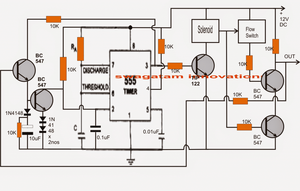 As per the corrective suggestions the above circuit is modified as shown below, please refer to the comments for the details:
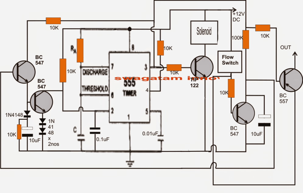
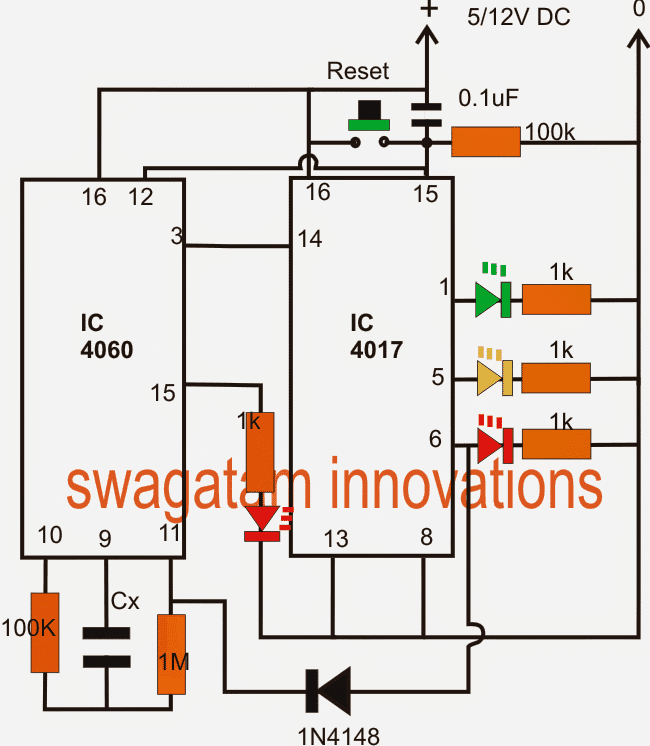
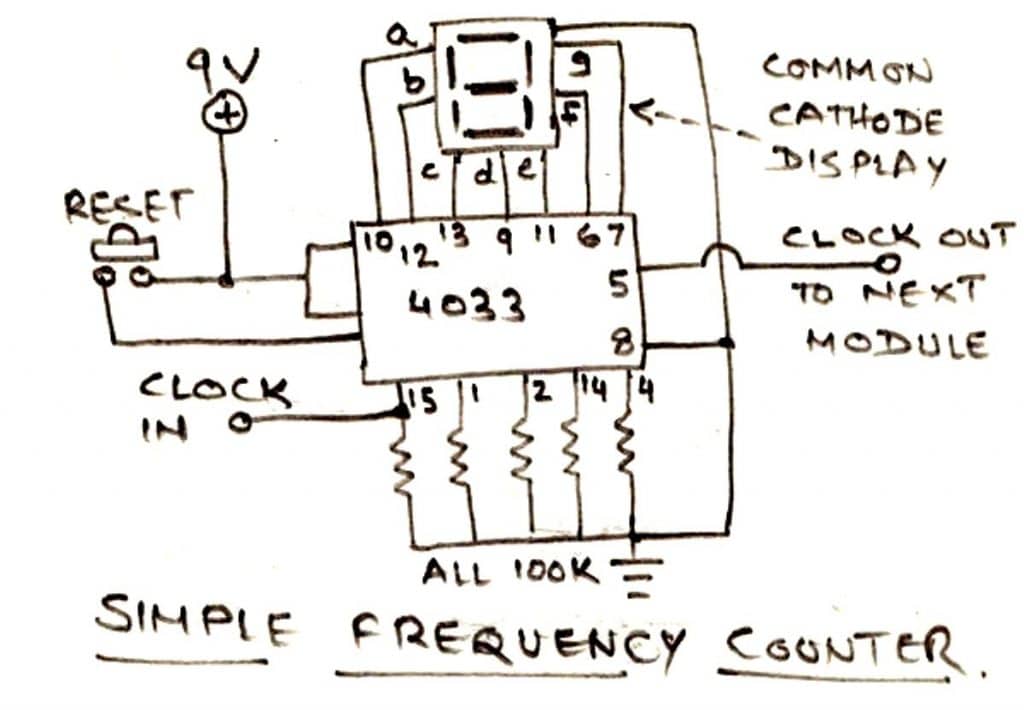
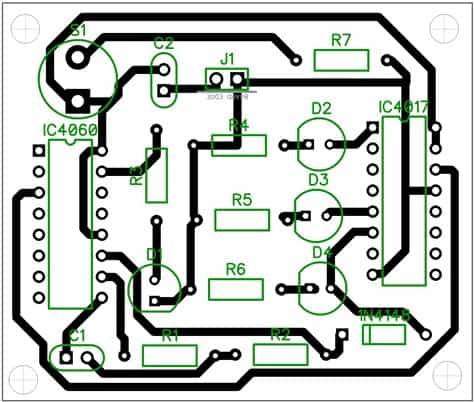
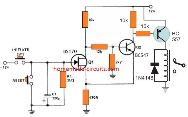 In the stand-by powered mode, the FET Q1 is in the switched ON condition, the BJT Q2 remains switch OFF, and the relay will be deactivated in its N/C position.
As soon as the timer is initiated by pressing the "initiate" switch, the capacitor C1 begins charging rapidly with the -12 V, which cuts off the FET and switches ON the BJT.
Now, when S1 is released, C1 begins slowly discharging through R1, until the potential across C1 drops to Vp of the FET.
At this instant Q1 turns ON again, and Q2 BJT turns OFF, reverting to its original standby state.
The relay now deactivates again
Much longer delays can be achieved by selecting an FET with lower Vp than 1.5 V, and higher values of C1.
The only drawback of the design s that, it works with a dual supply voltage.
In the stand-by powered mode, the FET Q1 is in the switched ON condition, the BJT Q2 remains switch OFF, and the relay will be deactivated in its N/C position.
As soon as the timer is initiated by pressing the "initiate" switch, the capacitor C1 begins charging rapidly with the -12 V, which cuts off the FET and switches ON the BJT.
Now, when S1 is released, C1 begins slowly discharging through R1, until the potential across C1 drops to Vp of the FET.
At this instant Q1 turns ON again, and Q2 BJT turns OFF, reverting to its original standby state.
The relay now deactivates again
Much longer delays can be achieved by selecting an FET with lower Vp than 1.5 V, and higher values of C1.
The only drawback of the design s that, it works with a dual supply voltage.
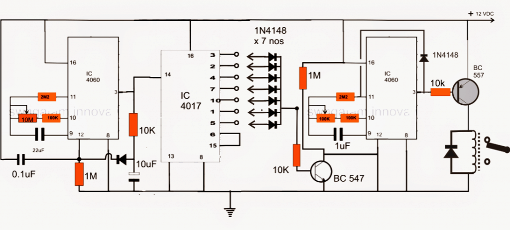
 A good way to fine-tune it, without dealing with a complete day/night period, is to hold off until around 10 minutes following sunset, at the center rotation between day and night, and alter R1 in order that the voltage across it is half the supply voltage.
Later, examine that the IC1 output is high during night and low during the daytime.
A low-pass filter is created using R2 and C1 , producing roughly a 1-second hold up to ensure the circuit doesn't get rattled with lightning flashes or various other brief light variations.
A 555 timer, ICI, is employed like a light level sensor; instead of the comparator circuit.
The 555 offers hysteresis, which implies that the trigger ON voltage will be greater than the trigger-off voltage.
This prevents the circuit from "stuttering" to and fro between off and on during transition thresholds.
The second IC in the circuit (IC2) is a 4017 (CD4017) CMOS decade counter.
Simply by hooking up output Q8 to the reset input, we allow it to count upto 7 and then start off yet again, therefore its output creates a solitary day-long pulse each week.
You are able to supply this to additional counters in order to calculate even extended time periods.
For instance, incorporating a divide-by-four counter (like a 4017 with Q5 attached to reset) could give you a period of 28 days
A good way to fine-tune it, without dealing with a complete day/night period, is to hold off until around 10 minutes following sunset, at the center rotation between day and night, and alter R1 in order that the voltage across it is half the supply voltage.
Later, examine that the IC1 output is high during night and low during the daytime.
A low-pass filter is created using R2 and C1 , producing roughly a 1-second hold up to ensure the circuit doesn't get rattled with lightning flashes or various other brief light variations.
A 555 timer, ICI, is employed like a light level sensor; instead of the comparator circuit.
The 555 offers hysteresis, which implies that the trigger ON voltage will be greater than the trigger-off voltage.
This prevents the circuit from "stuttering" to and fro between off and on during transition thresholds.
The second IC in the circuit (IC2) is a 4017 (CD4017) CMOS decade counter.
Simply by hooking up output Q8 to the reset input, we allow it to count upto 7 and then start off yet again, therefore its output creates a solitary day-long pulse each week.
You are able to supply this to additional counters in order to calculate even extended time periods.
For instance, incorporating a divide-by-four counter (like a 4017 with Q5 attached to reset) could give you a period of 28 days

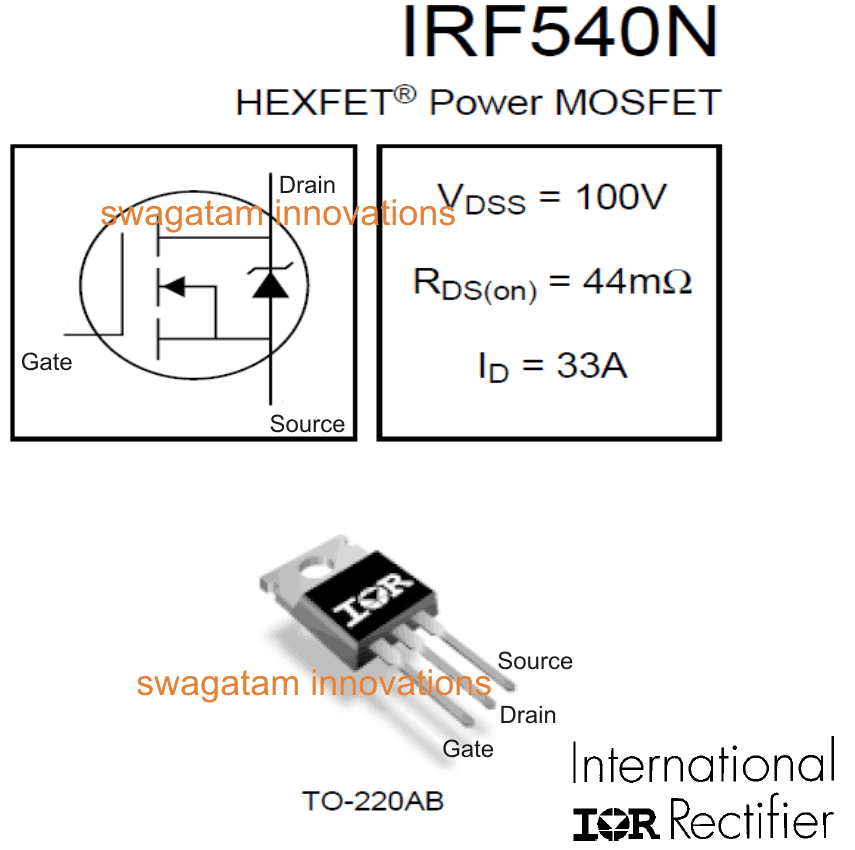 The trigger instantly switches ON the mosfet so that the load connected at its drain arm becomes fully ON and operative.
With awiper deviceattachedto this point would make it wipe for so long the switchedremainsdepressed.
A wiper system sometimes requires a delay feature for enabling a few minutes of wiping action before stopping.
With a small modification, the above circuit can be simply turned into a delay OFF circuit.
The trigger instantly switches ON the mosfet so that the load connected at its drain arm becomes fully ON and operative.
With awiper deviceattachedto this point would make it wipe for so long the switchedremainsdepressed.
A wiper system sometimes requires a delay feature for enabling a few minutes of wiping action before stopping.
With a small modification, the above circuit can be simply turned into a delay OFF circuit.
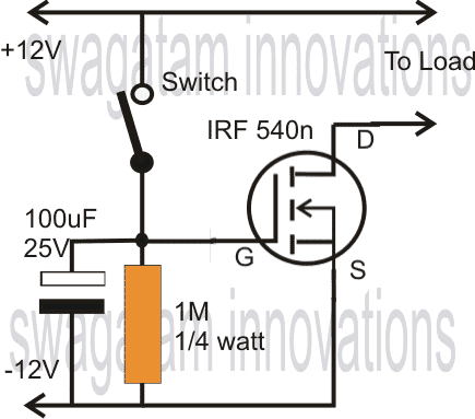 Video Demonstration
When the switch is toggled OFF, the load continues to receive the power since the stored voltage in the capacitor sustains the gate voltage and keeps it switched ON.
However the capacitor gradually discharges via the 1M resistor and when the voltage drop below 3V, the mosfet is no longer able to hold, and the complete system switches OFF.
The delay period depends on the value of the capacitor and the resistor values, increasing any one of them or both increases the delay period proportionately.
Video Demonstration
When the switch is toggled OFF, the load continues to receive the power since the stored voltage in the capacitor sustains the gate voltage and keeps it switched ON.
However the capacitor gradually discharges via the 1M resistor and when the voltage drop below 3V, the mosfet is no longer able to hold, and the complete system switches OFF.
The delay period depends on the value of the capacitor and the resistor values, increasing any one of them or both increases the delay period proportionately.
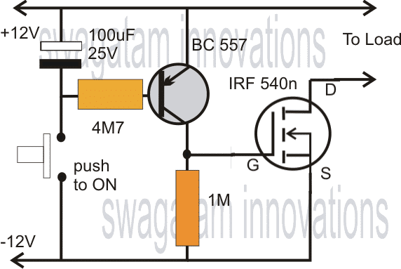
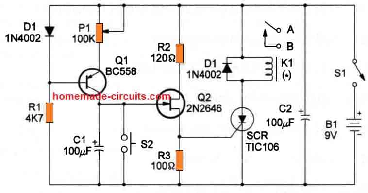 The diagram above shows basic MOSFET timer circuit.
 If you are interested to achieve a programmable feature from the above set up, you just need to appropriately calculate, assess and integrate the relevant pin outs from the corresponding ICs to the SET Resest Latch circuit input trigger terminals, as explained below:
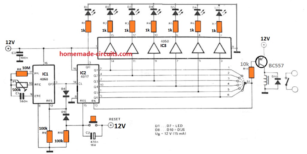 The main element of the timing circuit is a 4060 CMOS device, which is made up of an oscillator along with a 14 stage divider.
The frequency of the oscillator could be tweaked through potentiometer P1 in order that the output at Q13 is around a single pulse each hour.
The period of this clock beat could be extremely quick (around 100 ns), as it additionally resets the whole 4060 IC by way of diode D8.
The 'once each hour' clock pulse is given to the 2nd (divide-by-ten) counter, the 4017 IC.
One of several outputs of this counter is going to be logic high (logic one) at any given instant.
When the 4017 is reset, output Q0 goes high.
Right after one hour, output Q0 will turn low and output Q1 may become high, etc.
Switch S1 as a result allows the user to choose a time interval through one to six hours.
When the chosen output becomes high, the transistor turns off and the relay gets switched OFF (thus turning off the connected load).
Once the enable input of the 4017 is furthermore attached to the wiper of S1 any succeeding clock pulses turns out to have no impact on ihe counter.
The device will consequently continue to be in the switched OFF condition until the reset switch is presed by the user.
The 4050 CMOS buffer IC along with the 7 LEDs are incorporated to offer indication of the range of hours which may have essentially elapsed.
These parts could, obviously, be removed in case an lapsed time display is not needed.
The source voltage for this circuit is not really crucial and could be cover anything from 5 and 15 V, The current usage of the circuit, excluding the relay, will be in the range of 15 mA.
It is advisable to pick a source voltage that may be matching the specifications of the relay, to ensure that any problems are avoided.
The BC 557 transistor can handle a current of 70 mA, so make sure the relay coil voltage is rated withing this current range
The main element of the timing circuit is a 4060 CMOS device, which is made up of an oscillator along with a 14 stage divider.
The frequency of the oscillator could be tweaked through potentiometer P1 in order that the output at Q13 is around a single pulse each hour.
The period of this clock beat could be extremely quick (around 100 ns), as it additionally resets the whole 4060 IC by way of diode D8.
The 'once each hour' clock pulse is given to the 2nd (divide-by-ten) counter, the 4017 IC.
One of several outputs of this counter is going to be logic high (logic one) at any given instant.
When the 4017 is reset, output Q0 goes high.
Right after one hour, output Q0 will turn low and output Q1 may become high, etc.
Switch S1 as a result allows the user to choose a time interval through one to six hours.
When the chosen output becomes high, the transistor turns off and the relay gets switched OFF (thus turning off the connected load).
Once the enable input of the 4017 is furthermore attached to the wiper of S1 any succeeding clock pulses turns out to have no impact on ihe counter.
The device will consequently continue to be in the switched OFF condition until the reset switch is presed by the user.
The 4050 CMOS buffer IC along with the 7 LEDs are incorporated to offer indication of the range of hours which may have essentially elapsed.
These parts could, obviously, be removed in case an lapsed time display is not needed.
The source voltage for this circuit is not really crucial and could be cover anything from 5 and 15 V, The current usage of the circuit, excluding the relay, will be in the range of 15 mA.
It is advisable to pick a source voltage that may be matching the specifications of the relay, to ensure that any problems are avoided.
The BC 557 transistor can handle a current of 70 mA, so make sure the relay coil voltage is rated withing this current range
 The op amp timer circuit shown above accomplishes timing periods as much as 100 times more time compared to those accessible using regular circuits.
It achieves this by lowering the capacitor charging current through a factor of 100, consequently improving the charging time drastically, without requiring high value charging capacitors.
The circuit works in the following way:
When the start/reset button is clicked C1 gets discharged and this causes output of op amp IC1, which is configured as a voltage follower, to become zero volts.
The inverting input of comparator IC2 is at a reduced voltage level than the non -inverting input, hence the output of IC2 moves high.
The voltage around R4 is around 120 mV, which means that C1 charges via R2 with a current of approximately 120 nA, which apprers to be 100 times less than what could be attained in case R2 had been attached direct to positive supply.
Needless to say, if C1 had been charged through a consistent 120 mV it could rapidly achieve this voltage, and stop charging any further.
However, the lower terminal of R4 being fed back to the output of IC1 ensures that as the voltage across C1 goes up so does the output voltage and therefore the charging voltage given to R2.
Once the output voltage climbs to approximately 7.5 volts it surpasses the voltage refernced at the non-inverting input of IC2 by R6 and R7, and the output of IC2 becomes low.
A tiny quantity of positive feedback supplied by R8 inhibits any kind of noise existing on the output of IC1 from getting boosted by IC2 as it moves from the trigger point, because this normally produce false output pulses.
The timing length can be calculated by the equation:
T = R2 C1( 1 + R5/R4 + R5/R2) x C2 x ( 1 + R7/R6)
This may appear somewhat complex, but with the part numbers indicated the time interval can be set as long as 100 C1. Here C1 is in microfarads, let's say if C1 is selected as 1 ¦Ě then the output time interval will be 100 seconds.
It is very clear from the equation that it is possible to vary the timing interval linearly by substituting R2 with a 1 M potentiometer, or logarithmically by using a 10 k pot in place of R6 and R7.
The op amp timer circuit shown above accomplishes timing periods as much as 100 times more time compared to those accessible using regular circuits.
It achieves this by lowering the capacitor charging current through a factor of 100, consequently improving the charging time drastically, without requiring high value charging capacitors.
The circuit works in the following way:
When the start/reset button is clicked C1 gets discharged and this causes output of op amp IC1, which is configured as a voltage follower, to become zero volts.
The inverting input of comparator IC2 is at a reduced voltage level than the non -inverting input, hence the output of IC2 moves high.
The voltage around R4 is around 120 mV, which means that C1 charges via R2 with a current of approximately 120 nA, which apprers to be 100 times less than what could be attained in case R2 had been attached direct to positive supply.
Needless to say, if C1 had been charged through a consistent 120 mV it could rapidly achieve this voltage, and stop charging any further.
However, the lower terminal of R4 being fed back to the output of IC1 ensures that as the voltage across C1 goes up so does the output voltage and therefore the charging voltage given to R2.
Once the output voltage climbs to approximately 7.5 volts it surpasses the voltage refernced at the non-inverting input of IC2 by R6 and R7, and the output of IC2 becomes low.
A tiny quantity of positive feedback supplied by R8 inhibits any kind of noise existing on the output of IC1 from getting boosted by IC2 as it moves from the trigger point, because this normally produce false output pulses.
The timing length can be calculated by the equation:
T = R2 C1( 1 + R5/R4 + R5/R2) x C2 x ( 1 + R7/R6)
This may appear somewhat complex, but with the part numbers indicated the time interval can be set as long as 100 C1. Here C1 is in microfarads, let's say if C1 is selected as 1 ¦Ě then the output time interval will be 100 seconds.
It is very clear from the equation that it is possible to vary the timing interval linearly by substituting R2 with a 1 M potentiometer, or logarithmically by using a 10 k pot in place of R6 and R7.
 FIGURE:1
Phototransistor: It is actually a transistor which has its base current dependent on the light.
The collector current is = base current x gain of the device.
Reaction time is just around a few microseconds.
Photodarlington: When a couple of transistors in the same package are hooked up in a specific high gain configuration, it constitutes a Darlington.
In a photodarlington the first transistor is a phototransistor and the second one is any standard BJT.
Response time may be around hundredths of microseconds.
Detector area: It can be defined as the area (in square inches or millimeters) of the diode detector which accumulates the light.
The majority of PIN diodes use a plastic casing which works like a straightforward lens and gives a accumulation region of 0.01 to 0.025 square inches.
This region is very important while calculating the gain of the lens.
Inverse square law: This is actually the "key element" in almost all optical communications devices.
Simply said, it signifies that in case you increase the range across transmitter and the receiver, the capacity of the signal becomes proportionately lesser by the square of the distance.
As an example, if you obtain 9 microwatts of power with a 10 feet distance between the transmitter and receiver, you can expect to obtain just one microwatt of energy in case you raise the distance to 30 feet.
Transimpedance amplifier: It is an amplifier having an extremely low input impedance.
Often known as current-to-voltage converters, these special amplifiers in many cases can be found in optical devices.
Due to their low impedance load these guarantee optimum current through a photodiode.
They are able to offer a bandwidth up to a several hundred megahertz.
Lens gain: It is the ratio of the lens area to the detector area.
Given that the lens area is bigger than the detector area, a greater amount of light is collected from the lens.
Lens losses and focusing errors (which jointly amount to approximately 15%) should be taken into account while calculating the lens gain.
Infrared: It is the area of the light spectrum close to the red color (around 800 nanometers).
Many infrared LED's give off at either 880 nanometers or 940 nanometers.
The majority of silicon sensors show highest responsiveness at around 900 nanometers.
Infrared is employed mainly because almost all red (visible light) LED's don't find it easy to generate a 1 / 2 a milliwatt of power, although numerous IR LED's possess an output of 10 milliwatts or higher.
Collimate: This term refers to: aiming in a straight line.
Whenever light coming from a source moves through parallel beams rather than with a divergent cone, it is recognized as collimated.
Even though it is not possible to create a genuinely collimated beam, the lens of the transmitter makes an attempt to achieve this (see Fig.
2).
FIGURE:1
Phototransistor: It is actually a transistor which has its base current dependent on the light.
The collector current is = base current x gain of the device.
Reaction time is just around a few microseconds.
Photodarlington: When a couple of transistors in the same package are hooked up in a specific high gain configuration, it constitutes a Darlington.
In a photodarlington the first transistor is a phototransistor and the second one is any standard BJT.
Response time may be around hundredths of microseconds.
Detector area: It can be defined as the area (in square inches or millimeters) of the diode detector which accumulates the light.
The majority of PIN diodes use a plastic casing which works like a straightforward lens and gives a accumulation region of 0.01 to 0.025 square inches.
This region is very important while calculating the gain of the lens.
Inverse square law: This is actually the "key element" in almost all optical communications devices.
Simply said, it signifies that in case you increase the range across transmitter and the receiver, the capacity of the signal becomes proportionately lesser by the square of the distance.
As an example, if you obtain 9 microwatts of power with a 10 feet distance between the transmitter and receiver, you can expect to obtain just one microwatt of energy in case you raise the distance to 30 feet.
Transimpedance amplifier: It is an amplifier having an extremely low input impedance.
Often known as current-to-voltage converters, these special amplifiers in many cases can be found in optical devices.
Due to their low impedance load these guarantee optimum current through a photodiode.
They are able to offer a bandwidth up to a several hundred megahertz.
Lens gain: It is the ratio of the lens area to the detector area.
Given that the lens area is bigger than the detector area, a greater amount of light is collected from the lens.
Lens losses and focusing errors (which jointly amount to approximately 15%) should be taken into account while calculating the lens gain.
Infrared: It is the area of the light spectrum close to the red color (around 800 nanometers).
Many infrared LED's give off at either 880 nanometers or 940 nanometers.
The majority of silicon sensors show highest responsiveness at around 900 nanometers.
Infrared is employed mainly because almost all red (visible light) LED's don't find it easy to generate a 1 / 2 a milliwatt of power, although numerous IR LED's possess an output of 10 milliwatts or higher.
Collimate: This term refers to: aiming in a straight line.
Whenever light coming from a source moves through parallel beams rather than with a divergent cone, it is recognized as collimated.
Even though it is not possible to create a genuinely collimated beam, the lens of the transmitter makes an attempt to achieve this (see Fig.
2).
 FIGURE:2
Divergence: It is understood as the "dispersing off" of an optical ray.
Put simply, a diverging stream of light is the opposite of a collimated beam.
Just about all optical rays of light spread out in a divergent manner, some may do this a little more than others.
If you are able to create a ray of light having zero divergence (which is impossible), it simply would never comply with the inverse square law.
Meaning, it may be possible to direct a beam of light to an unlimited distance since the energy would be travelling without spreading or dispersing outward.
You will find very less divergence in laser beam lights, compared to other ordinary light sources.
Most of the spot lights are designed to have lower level of divergence, while flood lights have a huge amount of divergence (Fig2).
Responsivity: It is determined by the relationship between the optical and the electrical signal of a detector.
Generally, this value for a PIN diode can be 0.4 amps to 0.6 amps per watt.
Therefore, if a 1 mW light is incident on a PIN diode, we can expect a current outflow of 0.4 mA to 0.6 mA from it.
With regard to this attribute the proposed visible light beam communication might work using a current level of 100 pA, or using an optical power of 200 pW.
AC and DC Light: When you switch a LED lamp by toggling it ON and OFF, you are basically generating an AC like light source from the LED lamp.
If you illuminate it with a constant DC, then it becomes a DC source of light.
This phenomenon is important since most of the light source may have some traces of AC and some DC in them.
The flashlights using incandescent light bulb, exhibit a high quantity of DC light and a low quantity of AC light through them.
Our sun light is composed huge amounts of AC as well as DC light in it.
Fluorescent lamps emit some DC but a lot of AC.
In the proposed visible light communication circuit, the above phenomenon is crucial because, operating a DC based optical receiver may come across a plenty of AC light sources including sun light, which can rapidly saturate the receiver detection capacity and the actual detection of our AC communication signal can get hampered.
To overcome this issue, some sort of light shield will need to be installed which are commonly used in our cameras etc
f number or lens speed: In glass lenses the focal length to its diameter ratio is termed as the "f" number (f = fl/d).
Smaller f number determines a faster and more expensive lens.
You can easily imagine this figure as the optical "acceptance" angle (Fig3).
The feature becomes useful while selecting the transmitter len's collimating function.
FIGURE:2
Divergence: It is understood as the "dispersing off" of an optical ray.
Put simply, a diverging stream of light is the opposite of a collimated beam.
Just about all optical rays of light spread out in a divergent manner, some may do this a little more than others.
If you are able to create a ray of light having zero divergence (which is impossible), it simply would never comply with the inverse square law.
Meaning, it may be possible to direct a beam of light to an unlimited distance since the energy would be travelling without spreading or dispersing outward.
You will find very less divergence in laser beam lights, compared to other ordinary light sources.
Most of the spot lights are designed to have lower level of divergence, while flood lights have a huge amount of divergence (Fig2).
Responsivity: It is determined by the relationship between the optical and the electrical signal of a detector.
Generally, this value for a PIN diode can be 0.4 amps to 0.6 amps per watt.
Therefore, if a 1 mW light is incident on a PIN diode, we can expect a current outflow of 0.4 mA to 0.6 mA from it.
With regard to this attribute the proposed visible light beam communication might work using a current level of 100 pA, or using an optical power of 200 pW.
AC and DC Light: When you switch a LED lamp by toggling it ON and OFF, you are basically generating an AC like light source from the LED lamp.
If you illuminate it with a constant DC, then it becomes a DC source of light.
This phenomenon is important since most of the light source may have some traces of AC and some DC in them.
The flashlights using incandescent light bulb, exhibit a high quantity of DC light and a low quantity of AC light through them.
Our sun light is composed huge amounts of AC as well as DC light in it.
Fluorescent lamps emit some DC but a lot of AC.
In the proposed visible light communication circuit, the above phenomenon is crucial because, operating a DC based optical receiver may come across a plenty of AC light sources including sun light, which can rapidly saturate the receiver detection capacity and the actual detection of our AC communication signal can get hampered.
To overcome this issue, some sort of light shield will need to be installed which are commonly used in our cameras etc
f number or lens speed: In glass lenses the focal length to its diameter ratio is termed as the "f" number (f = fl/d).
Smaller f number determines a faster and more expensive lens.
You can easily imagine this figure as the optical "acceptance" angle (Fig3).
The feature becomes useful while selecting the transmitter len's collimating function.
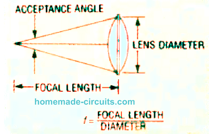 FIGURE:3
In cameras, which are designed to work with a fixed focal length, utilizes one lens that has a bigger diameter and another that has a smaller "f' number for a faster response.
This ensures that the larger lens is able to accumulate more quantity of light and the shutter is set to a faster speed than the smaller lens.
Table 1 can be referred for getting the "f" numbers vs.
acceptance angles information.
FIGURE:3
In cameras, which are designed to work with a fixed focal length, utilizes one lens that has a bigger diameter and another that has a smaller "f' number for a faster response.
This ensures that the larger lens is able to accumulate more quantity of light and the shutter is set to a faster speed than the smaller lens.
Table 1 can be referred for getting the "f" numbers vs.
acceptance angles information.
 Thermal noise: Even though thermal noise is not actually relevant to optical products for example lenses, the electronic functionality of the optical system could be restricted by thermal noise.
Thermal noise is induced in an electrical system through the arbitrary motion of molecules.
The thermal current noise (IN) of a resistor can be expressed by the equation:
(IN)2 = 4KTB/R
where K = Boltzmann's constant (1.38 x 10⁻²³)
T = temperature in Kelvin (300)
B = bandwidth in Hertz
R = resistance in ohms
A 300K resistor powered at around room temperature inside the receiver having a bandwidth of 20 kHz should eihibit a thermal noise current of 33 picoamps.
Despite the fact that 33 picoamps probably won't seem like a great deal of current, the noise may boost at the transimpedance amplifier output to as high as approximately 10 microvolts (RMS).
Converting this to peak-to-peak noise provides around 60 microvolts peak-to-peak.
In the light communication circuit, the sole amplifier between the transimpedance amplifier and the comparator is actually a differential amplifier using a gain of approximately 50. This amplifier amplifies the 60 microvolts noise and generates around 3 millivolts noise at the optical amp output.
Precise readings confirm a generation of 5 millivolts of noise.
This is acceptable since additional noise-producing elements exist in the unit, like the current amplification noise from the 1st transistor.
Though just about every transistor generates little noise, the first one generates excessive noise due to its greater signal amplification.
The significance of presenting equations such as this is that they provide us awareness for system enhancement and corrections.
If we had no issues of noise, practically endless distances could possibly be reached.
Nevertheless, if the signal strength is smaller than the noise, then that can be bad news for the experimenter.
We are able to deal with temperature issue at some level, and the equation indicates that when the temperature is lower, the noise is also lower.
However decreasing the transimpedance resistor temperature even by 100 degrees Kelvin might cause a reduction in the noise power by only a factor of approximately 1.2.
When an optical unit has a specifications of just a small amount of bandwidth of maybe a few hertz, such as a television remote control, we're able to reduce the bandwidth from 20 kHz to 20 Hertz and reduce the noise by a factor of approximately 30. Even while the inverse square rule running against us, that could cause an enhanced range through a factor of around 5.
This kind of reduction in the bandwidth might call for a decent tunable filter, which anyhow can be achieved.
Obviously, audio signals directed through a link using a 20 Hz bandwidth wouldn't be identifiable as audio.
However, it might enable a Morse-code transmission.
Photodetector: It is a semiconductor device designed to transform light into an electrical signal.
All devices like phototransistors, photo SCR's, phototriacs photocells, solar cells, and photodiodes fall under this category of photodetector.
Even parts like photoresistors and thermocouples could be generally regarded as varieties of photodetectors.
Phototransistors and photo-Darlington sensors are generally accustomed to detect light.
Both of these devices do the job well in case high speed detection is not a necessity.
Normal phototransistor have a switching period of 1 to 5 microseconds.
For Darlington types this figure may be around hundreds of microseconds.
Thermal noise: Even though thermal noise is not actually relevant to optical products for example lenses, the electronic functionality of the optical system could be restricted by thermal noise.
Thermal noise is induced in an electrical system through the arbitrary motion of molecules.
The thermal current noise (IN) of a resistor can be expressed by the equation:
(IN)2 = 4KTB/R
where K = Boltzmann's constant (1.38 x 10⁻²³)
T = temperature in Kelvin (300)
B = bandwidth in Hertz
R = resistance in ohms
A 300K resistor powered at around room temperature inside the receiver having a bandwidth of 20 kHz should eihibit a thermal noise current of 33 picoamps.
Despite the fact that 33 picoamps probably won't seem like a great deal of current, the noise may boost at the transimpedance amplifier output to as high as approximately 10 microvolts (RMS).
Converting this to peak-to-peak noise provides around 60 microvolts peak-to-peak.
In the light communication circuit, the sole amplifier between the transimpedance amplifier and the comparator is actually a differential amplifier using a gain of approximately 50. This amplifier amplifies the 60 microvolts noise and generates around 3 millivolts noise at the optical amp output.
Precise readings confirm a generation of 5 millivolts of noise.
This is acceptable since additional noise-producing elements exist in the unit, like the current amplification noise from the 1st transistor.
Though just about every transistor generates little noise, the first one generates excessive noise due to its greater signal amplification.
The significance of presenting equations such as this is that they provide us awareness for system enhancement and corrections.
If we had no issues of noise, practically endless distances could possibly be reached.
Nevertheless, if the signal strength is smaller than the noise, then that can be bad news for the experimenter.
We are able to deal with temperature issue at some level, and the equation indicates that when the temperature is lower, the noise is also lower.
However decreasing the transimpedance resistor temperature even by 100 degrees Kelvin might cause a reduction in the noise power by only a factor of approximately 1.2.
When an optical unit has a specifications of just a small amount of bandwidth of maybe a few hertz, such as a television remote control, we're able to reduce the bandwidth from 20 kHz to 20 Hertz and reduce the noise by a factor of approximately 30. Even while the inverse square rule running against us, that could cause an enhanced range through a factor of around 5.
This kind of reduction in the bandwidth might call for a decent tunable filter, which anyhow can be achieved.
Obviously, audio signals directed through a link using a 20 Hz bandwidth wouldn't be identifiable as audio.
However, it might enable a Morse-code transmission.
Photodetector: It is a semiconductor device designed to transform light into an electrical signal.
All devices like phototransistors, photo SCR's, phototriacs photocells, solar cells, and photodiodes fall under this category of photodetector.
Even parts like photoresistors and thermocouples could be generally regarded as varieties of photodetectors.
Phototransistors and photo-Darlington sensors are generally accustomed to detect light.
Both of these devices do the job well in case high speed detection is not a necessity.
Normal phototransistor have a switching period of 1 to 5 microseconds.
For Darlington types this figure may be around hundreds of microseconds.
 The data here is provided with a consideration that no light is assimilated or reflected by the lens, and the detector is positioned exactly at the focal point of the lens.
These considerations can be obviously inconsistent, since even the best quality camera lenses, that are layered with anti-reflective coatings, never allow 100 percent light to pass.
There may be ample room here for trials.
Several elementary tests revealed that around 85% of the calculative or assumptive gain is achievable.
The data here is provided with a consideration that no light is assimilated or reflected by the lens, and the detector is positioned exactly at the focal point of the lens.
These considerations can be obviously inconsistent, since even the best quality camera lenses, that are layered with anti-reflective coatings, never allow 100 percent light to pass.
There may be ample room here for trials.
Several elementary tests revealed that around 85% of the calculative or assumptive gain is achievable.
 FIGURE:4
The FM transmitter circuit stage, shown in Fig.
5, is made up of a microphone amplifier (Q1 and Q2) and an FM modulator created through a 555 timer (IC1).
You can find a couple of setting options, one for the FM center frequency (R11) and the other for adjusting the level of deviation (R4).
FIGURE:4
The FM transmitter circuit stage, shown in Fig.
5, is made up of a microphone amplifier (Q1 and Q2) and an FM modulator created through a 555 timer (IC1).
You can find a couple of setting options, one for the FM center frequency (R11) and the other for adjusting the level of deviation (R4).
 The PIN diode detector (D1) can be seen connected through AC signal with a basic transimpedance amplifier comprising Q1 and Q2. Although the signal is coupled through an AC signal, the biasing for the PIN diode has to be DC coupled.
This is accomplished by means of resistors R1 and R2.
If the proposed light communication circuit is operated in a excessive background light condition, resistor R1 may need to be decreased in value to stop DC saturation of the PIN diode.
In case the DC voltage across R1 is higher than around 3 volts during functioning, it may be a good idea to reduce the value of R1. The transimpedance resistors (R4 and R5) determine the actual gain of the amplifier.
A couple of series resistors were employed rather than just a single since each resistor has its own capacitance across themselves.
By using pair of resistors allows the reduction in the capacitance with a factor of two.
All that is needed is to connect the two resistors over the PCB.
The transimpedance amplifier output is nothing but its input current multiplied by the transimpedance resistance.
For this reason it's occasionally known as current-to-voltage converter.
When you increase the resistance value, the signal also boosts, however the bandwidth diminishes.
Because the signal boosts directly in response to the resistance value, and we also have an increasing noise by the square root of the resistance.
It seems sensible to use a resistance that's as big as it possibly can be, provided you continue to have sufficient bandwidth.
For this reason Q1 has to be a VHF transistor.
Because the signal's center frequency is at 50 kHz, it's advisable to restrict the optical amp's bandwidth to minimize the overall noise.
Transistor Q3 along with the encircling parts constitute a two-way high-pass filter at around 40 kHz.
This gets rid of the low frequency noise, for example like the 50/60 hertz optical noise emitted by our home lights.
Transistor Q4 as well as the connected circuitry create a 60 kHz low-pass filter.
This eradicates high-frequency electrical noise for example those emanating from many AM radio stations.
When we integrate the low-pass and highpass filters, they give rise to a bandpass filter structured around 50 kHz, having a pass band of approximately 20 kHz.
It may be possible to cut down the noise by creating a narrower filter, between the optical amp's output and the demodulation stage input.
The drawback is may be that the narrow filter will need to be tunable, and will require a scope for setting it up.
Transistors Q5 and Q6 are used for designing a differential amplifier which is actually the gain stage of the optical amplifier, apart from Q1.
The function of a differential amplifier is to ensure that a differential signal is avaialble to operate the voltage comparator.
It can be great to operate a comparator differentially as you are able to acquire two times the signal without inducing two times noise.
However, there exists one issue with a differential amplifier: if a reasonable amount of gain is required, the transistors has to be nicely matched up.
This inhibits one transistor from "going into a thermal runaway" and saturating.
The matching of transistors can be done using the circuit in Fig.
7.
The PIN diode detector (D1) can be seen connected through AC signal with a basic transimpedance amplifier comprising Q1 and Q2. Although the signal is coupled through an AC signal, the biasing for the PIN diode has to be DC coupled.
This is accomplished by means of resistors R1 and R2.
If the proposed light communication circuit is operated in a excessive background light condition, resistor R1 may need to be decreased in value to stop DC saturation of the PIN diode.
In case the DC voltage across R1 is higher than around 3 volts during functioning, it may be a good idea to reduce the value of R1. The transimpedance resistors (R4 and R5) determine the actual gain of the amplifier.
A couple of series resistors were employed rather than just a single since each resistor has its own capacitance across themselves.
By using pair of resistors allows the reduction in the capacitance with a factor of two.
All that is needed is to connect the two resistors over the PCB.
The transimpedance amplifier output is nothing but its input current multiplied by the transimpedance resistance.
For this reason it's occasionally known as current-to-voltage converter.
When you increase the resistance value, the signal also boosts, however the bandwidth diminishes.
Because the signal boosts directly in response to the resistance value, and we also have an increasing noise by the square root of the resistance.
It seems sensible to use a resistance that's as big as it possibly can be, provided you continue to have sufficient bandwidth.
For this reason Q1 has to be a VHF transistor.
Because the signal's center frequency is at 50 kHz, it's advisable to restrict the optical amp's bandwidth to minimize the overall noise.
Transistor Q3 along with the encircling parts constitute a two-way high-pass filter at around 40 kHz.
This gets rid of the low frequency noise, for example like the 50/60 hertz optical noise emitted by our home lights.
Transistor Q4 as well as the connected circuitry create a 60 kHz low-pass filter.
This eradicates high-frequency electrical noise for example those emanating from many AM radio stations.
When we integrate the low-pass and highpass filters, they give rise to a bandpass filter structured around 50 kHz, having a pass band of approximately 20 kHz.
It may be possible to cut down the noise by creating a narrower filter, between the optical amp's output and the demodulation stage input.
The drawback is may be that the narrow filter will need to be tunable, and will require a scope for setting it up.
Transistors Q5 and Q6 are used for designing a differential amplifier which is actually the gain stage of the optical amplifier, apart from Q1.
The function of a differential amplifier is to ensure that a differential signal is avaialble to operate the voltage comparator.
It can be great to operate a comparator differentially as you are able to acquire two times the signal without inducing two times noise.
However, there exists one issue with a differential amplifier: if a reasonable amount of gain is required, the transistors has to be nicely matched up.
This inhibits one transistor from "going into a thermal runaway" and saturating.
The matching of transistors can be done using the circuit in Fig.
7.
 FIGURE:8
An LM311 comparator (IC1) switches the somewhat low analog signal to a digital signal for the CD4046 phase-locked loop (IC2).
It must be noted that the amplitude of the retrieved acoustic signal is not relevant to the amplitude of the received signal.
The amplitude of the retrieved audio is dependent only on the quantity of frequency deviation established by the transmitter and also the amplitude of the operator's voice.
The phase-locked loop (IC2) is set up like a first-order FM demodulator.
Without applying any input signal, the center frequency of the network comprising IC2 pin 3 which is also TP3 is fine-tuned using R8 to set for a 50 kHz frequency.
Due to the fact that the differences between the CD4046 brands could be quite significant, it may be necessary to modify R7 and, possibly, R9 also.
The demodulated output through IC2 is filtered using a Q1 based 3 kHz low-pass filter.
This signal is subsequently fed to audio power amplifier built using LM386 amplifier.
FIGURE:8
An LM311 comparator (IC1) switches the somewhat low analog signal to a digital signal for the CD4046 phase-locked loop (IC2).
It must be noted that the amplitude of the retrieved acoustic signal is not relevant to the amplitude of the received signal.
The amplitude of the retrieved audio is dependent only on the quantity of frequency deviation established by the transmitter and also the amplitude of the operator's voice.
The phase-locked loop (IC2) is set up like a first-order FM demodulator.
Without applying any input signal, the center frequency of the network comprising IC2 pin 3 which is also TP3 is fine-tuned using R8 to set for a 50 kHz frequency.
Due to the fact that the differences between the CD4046 brands could be quite significant, it may be necessary to modify R7 and, possibly, R9 also.
The demodulated output through IC2 is filtered using a Q1 based 3 kHz low-pass filter.
This signal is subsequently fed to audio power amplifier built using LM386 amplifier.
 LM386 Amplifier Circuit
A larger bandwidth could be achieved by making the filter tp pass higher frequency.
Since the "carrier" frequency is just 50 kHz, make sure not to expand the audio bandwidth to higher than 6 or 7 kHz.
LM386 Amplifier Circuit
A larger bandwidth could be achieved by making the filter tp pass higher frequency.
Since the "carrier" frequency is just 50 kHz, make sure not to expand the audio bandwidth to higher than 6 or 7 kHz.
 OPTICAL DEMODULATOR AND AUDIO AMPLIFIER CIRCUIT.
PLEASE NOTE THAT IN THE ABOVE PCB DESIGN, THE IC3 IS NOT AN LM386 BASED AMPLIFIER, RATHER SOME OTHER IC WHICH IS OBSOLETE NOW.
PLEASE ADJUST THE AMPLIFIER SECTION WITH AN LM386 CIRCUIT BY REPLACING IC3 WITH LM386, AND BY SUITABLY ADJUSTING THE COMPONENTS AROUND IC3.
OPTICAL DEMODULATOR AND AUDIO AMPLIFIER CIRCUIT.
PLEASE NOTE THAT IN THE ABOVE PCB DESIGN, THE IC3 IS NOT AN LM386 BASED AMPLIFIER, RATHER SOME OTHER IC WHICH IS OBSOLETE NOW.
PLEASE ADJUST THE AMPLIFIER SECTION WITH AN LM386 CIRCUIT BY REPLACING IC3 WITH LM386, AND BY SUITABLY ADJUSTING THE COMPONENTS AROUND IC3.
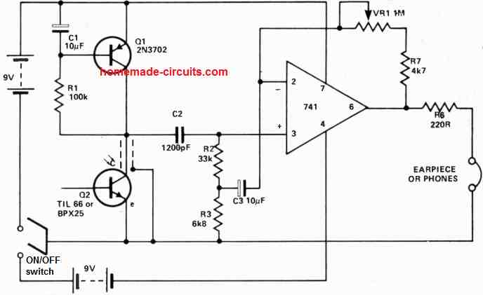

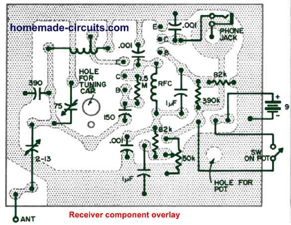 The detector stage is very sensitive and selective with its characteristics.
This stage will receives not just code impulses but additionally SSB and AM phone.
Any individual accustomed to sophisticated receiver systems, could be amazed with the working ability of this simple receiver circuit.
The detector stage is very sensitive and selective with its characteristics.
This stage will receives not just code impulses but additionally SSB and AM phone.
Any individual accustomed to sophisticated receiver systems, could be amazed with the working ability of this simple receiver circuit.
 This 3.5 MHz regenerative receiver is designed to self optimize and adjust the LC tank circuit ratio value resulting in an enhanced tuning ans selectivity.
 This resistor isn't significant and just about any value above 50 k will be enough.
Tr1 works like an impedance modifier providing current amplification only, which may include around 30% voltage loss.
VR1 attached to the Tr1 source adjusts the audio output and therefore the deviation, by following the source of TR1 towards the Tr2 base through C3.
Tr2 produces voltage gain, and by integrating the upper bias chain with the its collector, some level of feedback is achieved, which restricts the gain to around 100 times.
R8 and C5 function as a decoupling network for the modulator towards the power supply side and R7, while C6 holds RF away from the modulator output.
R6 and C4 provide the some additional trimming to the circuit to accomplish the necessary falling characteristic to the audio results.
The current requirement for the modulator is approximately 500 ¦ĚA.
This resistor isn't significant and just about any value above 50 k will be enough.
Tr1 works like an impedance modifier providing current amplification only, which may include around 30% voltage loss.
VR1 attached to the Tr1 source adjusts the audio output and therefore the deviation, by following the source of TR1 towards the Tr2 base through C3.
Tr2 produces voltage gain, and by integrating the upper bias chain with the its collector, some level of feedback is achieved, which restricts the gain to around 100 times.
R8 and C5 function as a decoupling network for the modulator towards the power supply side and R7, while C6 holds RF away from the modulator output.
R6 and C4 provide the some additional trimming to the circuit to accomplish the necessary falling characteristic to the audio results.
The current requirement for the modulator is approximately 500 ¦ĚA.
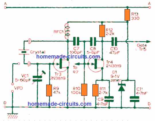 VC1 is positioned to drag the crystal to a particular frequency and does not cause any effect on the VFO.
RFC1 inhibits the signal from passing to Tr3, by allowing it to pass through C7 towards the TR4 gate, which is the phase modulator, having R12 as the load.
The output passes by means of C10 towards the multiplier chain, and the feedback passes via C8 generating the phase modulation.
The audio signal is given to the TR3 gate, 1V p/p being the minimum requirement by the phase modulator.
VC1 is positioned to drag the crystal to a particular frequency and does not cause any effect on the VFO.
RFC1 inhibits the signal from passing to Tr3, by allowing it to pass through C7 towards the TR4 gate, which is the phase modulator, having R12 as the load.
The output passes by means of C10 towards the multiplier chain, and the feedback passes via C8 generating the phase modulation.
The audio signal is given to the TR3 gate, 1V p/p being the minimum requirement by the phase modulator.
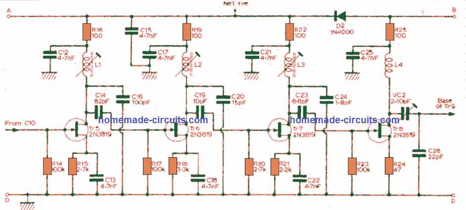 These stages are designed with similar layouts, and are used to resonate on the harmonic frequencies.
All these identical stages operate with quiescent currents of around 500 ¦ĚA.
If this is increased to 1.5 mA with an RF signal connected, they begin working in Class AB mode.
Since the FETs provide high input impedance, the output could be extracted from the drain, which helps to avoid the use tapping on the coils.
Since the loading is supposed to be negligible, this allows the circuit Q to remain high and ensures that tuning of the coils is not very complex.
The tuning for the output of the power amplifier is over a sharp range.
Therefore, VC2 needs to be very meticulously adjusted to get the finest results.
A tiny metal shielding is essential around L4, to stop feedback from reaching L3, which may otherwise result in induced oscillation, negatively affecting the efficiency of the stage.
R24 works like a current limiter and voltage feedback generator for Tr8.
These stages are designed with similar layouts, and are used to resonate on the harmonic frequencies.
All these identical stages operate with quiescent currents of around 500 ¦ĚA.
If this is increased to 1.5 mA with an RF signal connected, they begin working in Class AB mode.
Since the FETs provide high input impedance, the output could be extracted from the drain, which helps to avoid the use tapping on the coils.
Since the loading is supposed to be negligible, this allows the circuit Q to remain high and ensures that tuning of the coils is not very complex.
The tuning for the output of the power amplifier is over a sharp range.
Therefore, VC2 needs to be very meticulously adjusted to get the finest results.
A tiny metal shielding is essential around L4, to stop feedback from reaching L3, which may otherwise result in induced oscillation, negatively affecting the efficiency of the stage.
R24 works like a current limiter and voltage feedback generator for Tr8.
 The overall dissipation from the transistor Tr9 using a properly set multiplier chain and a dynamic crystal attached, could be up to 300 mW which means a little heat sink may be required to be installed with this transistor.
Tr10 must be mounted on the track side of the PCB.
Its input impedance is really low and capacitive in nature.
The C28 and VC3, are used for tuning L5 and create an impedance matching into the base of TR10. RFC4 helps to compensate for the input capacity and RFC5 acts like the DC return path.
Seeing that Tr10 may dissipate up to 2.5 Watts of power, a large heat sink may be required to keep this power transistor cool.
RFC6 is positioned to suppress RF to ensure that the output circuit configuration using VC4, C30, L6, C31, L7 and VC5 solely becomes the collector load for TR10. The screening shield put around L7 and VC5 helps to inhibit the output harmonic content significantly, and one should make sure this is included at all costs.
The overall dissipation from the transistor Tr9 using a properly set multiplier chain and a dynamic crystal attached, could be up to 300 mW which means a little heat sink may be required to be installed with this transistor.
Tr10 must be mounted on the track side of the PCB.
Its input impedance is really low and capacitive in nature.
The C28 and VC3, are used for tuning L5 and create an impedance matching into the base of TR10. RFC4 helps to compensate for the input capacity and RFC5 acts like the DC return path.
Seeing that Tr10 may dissipate up to 2.5 Watts of power, a large heat sink may be required to keep this power transistor cool.
RFC6 is positioned to suppress RF to ensure that the output circuit configuration using VC4, C30, L6, C31, L7 and VC5 solely becomes the collector load for TR10. The screening shield put around L7 and VC5 helps to inhibit the output harmonic content significantly, and one should make sure this is included at all costs.
 All component leads are inserted up to the neck and kept as small as it can be, while the extended legs of coils and resistors must be appropriately grounded.
The coils must be built with the help of the recommended drill shafts,
After the winding on the drill is done, the coil should be forced over the stiff former, then the space between the turns must be adjusted by stretching exactly to the recommended overall length of the coil.,
Finally, the coils must be secured in place over the formers by applying a very mild layer of epoxy resin adhesive.
Coils that are recommended to have adjustable iron slugs must be secured in the set position with the help of a melted wax drop.
All the top end holes of these coils must be countersunk, using a appropriate drill bit.
Construction is commenced first by fixing the PCB inside the die-cast container and drilling the bolting holes through the board and the base.
Next begin assembling the components by soldering as shown in Fig.
6, from the long axis outwards.
All component leads are inserted up to the neck and kept as small as it can be, while the extended legs of coils and resistors must be appropriately grounded.
The coils must be built with the help of the recommended drill shafts,
After the winding on the drill is done, the coil should be forced over the stiff former, then the space between the turns must be adjusted by stretching exactly to the recommended overall length of the coil.,
Finally, the coils must be secured in place over the formers by applying a very mild layer of epoxy resin adhesive.
Coils that are recommended to have adjustable iron slugs must be secured in the set position with the help of a melted wax drop.
All the top end holes of these coils must be countersunk, using a appropriate drill bit.
Construction is commenced first by fixing the PCB inside the die-cast container and drilling the bolting holes through the board and the base.
Next begin assembling the components by soldering as shown in Fig.
6, from the long axis outwards.
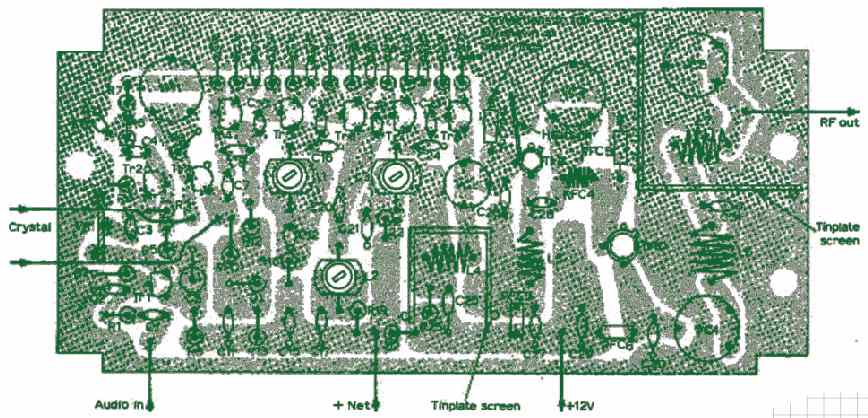 First solder the screens into position before everything to facilitate easy installation.
Additionally it may be a good idea to flip the PCB over, bolt it to the cover of the box, then drill holes through the center of the variable capacitors and coils with a No.60 drill.
These holes must be further made bigger to 6 mm to enable easy access to the respective trimmers during the final tuning process, after the PCB is installed inside the boxed.
The heatsink for the Tr10 can be any standard type available in the market, but for Tr9 this could be built manually by turning a 12 mm square of copper or tinplate with the help 5 mm drill mandrel and then pushing it around the transistor.
First solder the screens into position before everything to facilitate easy installation.
Additionally it may be a good idea to flip the PCB over, bolt it to the cover of the box, then drill holes through the center of the variable capacitors and coils with a No.60 drill.
These holes must be further made bigger to 6 mm to enable easy access to the respective trimmers during the final tuning process, after the PCB is installed inside the boxed.
The heatsink for the Tr10 can be any standard type available in the market, but for Tr9 this could be built manually by turning a 12 mm square of copper or tinplate with the help 5 mm drill mandrel and then pushing it around the transistor.
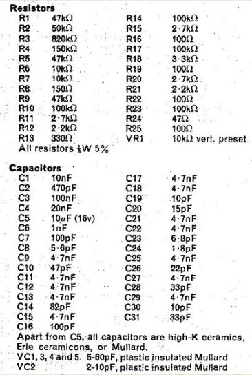


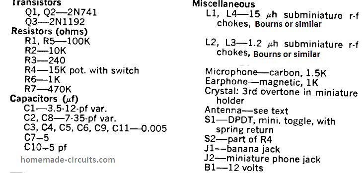
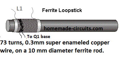
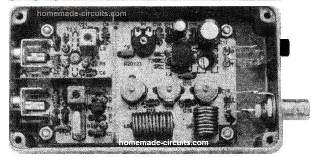
 The oscillator developed around FET T1 gets its frequency solidity through a quartz crystal, X1. Here, an low-cost third-overtone series resonance crystal is employed.
The oscillator is ˇ®forcedˇŻ to run on the third over-tone of the quartz'crystal by fine-tuning the L-C parallel tuned circuit from the drain line to 27 MHZ.
Capacitor C20 is necessary to guarantee satisfactory feedback in the oscillator, as well as boosts its start up actions.
Frequency modulation in a low deviation (NBFM) is accomplished using a adjustable capacitance diode ('varicapˇŻ), D1. The audio input signal (150 mVpp max.) is supplied to connector K1.
The oscillator signal activated on the secondary winding of L1 is given to the gate-1 terminal of MOSFET T2, a BF982.
Gate 2 of T2 is fixed at approximately 50 percent of the supply voltage through R2-R3 to attain highest amplification.
If AM [amplitude modulation; pretty uncommon though) is necessary, the modulation signal could be attached to K2 using a coupling capacitor.
The audio voltage may alter the gate 2 voltage of the MOSFET, resulting in linear [within limits!) gain control of the MOSFET.
The result is an amplitude-modulated RF output signal.
An sound level of 130 mVpp leads to a modulation depth of around 70 PERCENT.
The quiescent current of the power amplifier transistor, T3, is defined using the preset P1, which establishes the gate bias.
Observe that the preset's supply voltage is intensely decoupled to protect against supply and zener diode noise interfering'with the RF signal on the gate.
The RF power transistor is a HEXFET Type IRF52O from International Rectifier.
As presented, the transistor is thermally controlled with a heatsink.
The output filter is a basic pi-type low-pass created to minimize harmonics and complement the output transistor into a load of 50-Q, that is plugged into K3.
The oscillator developed around FET T1 gets its frequency solidity through a quartz crystal, X1. Here, an low-cost third-overtone series resonance crystal is employed.
The oscillator is ˇ®forcedˇŻ to run on the third over-tone of the quartz'crystal by fine-tuning the L-C parallel tuned circuit from the drain line to 27 MHZ.
Capacitor C20 is necessary to guarantee satisfactory feedback in the oscillator, as well as boosts its start up actions.
Frequency modulation in a low deviation (NBFM) is accomplished using a adjustable capacitance diode ('varicapˇŻ), D1. The audio input signal (150 mVpp max.) is supplied to connector K1.
The oscillator signal activated on the secondary winding of L1 is given to the gate-1 terminal of MOSFET T2, a BF982.
Gate 2 of T2 is fixed at approximately 50 percent of the supply voltage through R2-R3 to attain highest amplification.
If AM [amplitude modulation; pretty uncommon though) is necessary, the modulation signal could be attached to K2 using a coupling capacitor.
The audio voltage may alter the gate 2 voltage of the MOSFET, resulting in linear [within limits!) gain control of the MOSFET.
The result is an amplitude-modulated RF output signal.
An sound level of 130 mVpp leads to a modulation depth of around 70 PERCENT.
The quiescent current of the power amplifier transistor, T3, is defined using the preset P1, which establishes the gate bias.
Observe that the preset's supply voltage is intensely decoupled to protect against supply and zener diode noise interfering'with the RF signal on the gate.
The RF power transistor is a HEXFET Type IRF52O from International Rectifier.
As presented, the transistor is thermally controlled with a heatsink.
The output filter is a basic pi-type low-pass created to minimize harmonics and complement the output transistor into a load of 50-Q, that is plugged into K3.
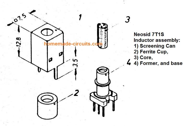 Closely wound internal diameter 8 mm; no core.
L6 is made up of 8 turns of 1-mm dia.
(SWG20] enameled copper wire.
Tightly wind internal diameter 8 mm; without core.
The PCB layout is supplied in Fig.
3.
Closely wound internal diameter 8 mm; no core.
L6 is made up of 8 turns of 1-mm dia.
(SWG20] enameled copper wire.
Tightly wind internal diameter 8 mm; without core.
The PCB layout is supplied in Fig.
3.
 lt must be taken into consideration that the board for 27 MHz transmitter circuit is double sided, but is not through-plated.
This implies that component leads has to be soldered from both sides of the PCB wherever applicable.
Furthermore, each and every part wires should be kept as small as feasible.
Commence by fitting inductors L1 and L3. Do not install the screening boxes as yet.
As suggested by their dashed lines on the PCB overlay.
Transistors T2 and T3 are fixed at the bottom side of the PCB.
This allows T3 to be safely placed to the base of the metallic housing where the PCB is fixed later on.
Remember to apply an insulating washer, because the metal tab of the IRF520 is coupled to the drain.
The type hint of T2 is legible from top area of the PCB.
The rest of the engineering is pretty basic, and should not bring about difficulties for those who have some expertise in developing RF or radio projects.
The audio input sockets are PCB-mount types.
The oscillator, buffer and power amplifier are shielded from each other by bits of 15-mm large tin sheet fixed top to bottom on the dashed lines around the PCB overlay.
As indicated in the opening picture of the prototype, the board is set up in a diecast enclosure.
Despite the fact that a BNC socket is used on the prototype, an SO-239 style is likewise well suited for the RF output.
The DC power supply input is created with a 2-way adapter outlet as utilized on portable radios.
lt must be taken into consideration that the board for 27 MHz transmitter circuit is double sided, but is not through-plated.
This implies that component leads has to be soldered from both sides of the PCB wherever applicable.
Furthermore, each and every part wires should be kept as small as feasible.
Commence by fitting inductors L1 and L3. Do not install the screening boxes as yet.
As suggested by their dashed lines on the PCB overlay.
Transistors T2 and T3 are fixed at the bottom side of the PCB.
This allows T3 to be safely placed to the base of the metallic housing where the PCB is fixed later on.
Remember to apply an insulating washer, because the metal tab of the IRF520 is coupled to the drain.
The type hint of T2 is legible from top area of the PCB.
The rest of the engineering is pretty basic, and should not bring about difficulties for those who have some expertise in developing RF or radio projects.
The audio input sockets are PCB-mount types.
The oscillator, buffer and power amplifier are shielded from each other by bits of 15-mm large tin sheet fixed top to bottom on the dashed lines around the PCB overlay.
As indicated in the opening picture of the prototype, the board is set up in a diecast enclosure.
Despite the fact that a BNC socket is used on the prototype, an SO-239 style is likewise well suited for the RF output.
The DC power supply input is created with a 2-way adapter outlet as utilized on portable radios.
 1)+5V
2) Ground
3)+D
4) -D
The+5V and ground are the supply out terminals which are normally used for powering the connected external device.
The +D, and -D are the data communication terminals which produces the complex differential signal across each other in a push-pull manner, meaning the +D is referenced to -D, while the -D signal is referenced to the +D terminals.
This is what makes transmitting Internet through LED so confusing and complex.
This forced me to think of an alternative and more efficient design, that could actually transmit an USB internet data through LED Li-Fi circuit, without distorting the actual signal, and by employing ordinary components.
After some thinking I came up with the following circuits which hopefully would enable transmitting internet through LED light.
For the transmitter I decided to use a simple differential amplifier circuit module using IC BD5460, the following image shows the basic layout of this amplifier circuit.
1)+5V
2) Ground
3)+D
4) -D
The+5V and ground are the supply out terminals which are normally used for powering the connected external device.
The +D, and -D are the data communication terminals which produces the complex differential signal across each other in a push-pull manner, meaning the +D is referenced to -D, while the -D signal is referenced to the +D terminals.
This is what makes transmitting Internet through LED so confusing and complex.
This forced me to think of an alternative and more efficient design, that could actually transmit an USB internet data through LED Li-Fi circuit, without distorting the actual signal, and by employing ordinary components.
After some thinking I came up with the following circuits which hopefully would enable transmitting internet through LED light.
For the transmitter I decided to use a simple differential amplifier circuit module using IC BD5460, the following image shows the basic layout of this amplifier circuit.
 I modified the design into the required Li-Fi transmitter circuit for making it compatible to internet signals, as shown below:
 We can see how the differential music input terminals are used for receiving the internet data, while the output is connected to an LED via a bridge rectifier.
Using a bridge rectifier appears to be a smart idea, otherwise it would be simply impossible to transmit the push-pull signals through a LED, since an LED would simply fail to differentiate between these two signals.
By using the bridge we have effectively enabled the LED to recognize both the halves of the USB signal and send it to the receiver without causing any distortions in the original content.
We can see how the differential music input terminals are used for receiving the internet data, while the output is connected to an LED via a bridge rectifier.
Using a bridge rectifier appears to be a smart idea, otherwise it would be simply impossible to transmit the push-pull signals through a LED, since an LED would simply fail to differentiate between these two signals.
By using the bridge we have effectively enabled the LED to recognize both the halves of the USB signal and send it to the receiver without causing any distortions in the original content.
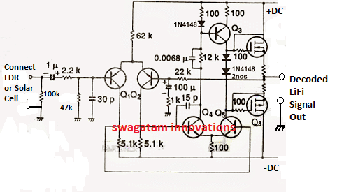 The BJTs and the mosfets can be any general propose rated to work with 12V/1amp supply.
However if you want a powerful decoded output you could very well keep the original values for the devices and enjoy a powerful LiFi decoded inernet output.
UPDATE:
In the discussed concept we used a class D amplifier for the LiFi transmitter, however a class D amplifier essentially involves PWM for processing the input, which could be highly undesirable for an internet data to go through.
We do not want to distort or modify the complex Internet data in any manner, therefore a class D amplifier perhaps cannot be applied for an internet LiFi.
As per my assumption we don't need a classD amplifier rather only a BTL amplifier, which does not involve a PWM function, an example design can be witnessed below using the IC TDA7052.
The BJTs and the mosfets can be any general propose rated to work with 12V/1amp supply.
However if you want a powerful decoded output you could very well keep the original values for the devices and enjoy a powerful LiFi decoded inernet output.
UPDATE:
In the discussed concept we used a class D amplifier for the LiFi transmitter, however a class D amplifier essentially involves PWM for processing the input, which could be highly undesirable for an internet data to go through.
We do not want to distort or modify the complex Internet data in any manner, therefore a class D amplifier perhaps cannot be applied for an internet LiFi.
As per my assumption we don't need a classD amplifier rather only a BTL amplifier, which does not involve a PWM function, an example design can be witnessed below using the IC TDA7052.
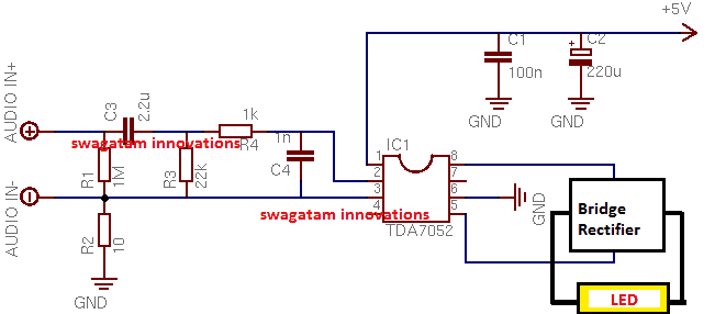 Now this looks perfect, and seems like the Internet data would be transferred to the LED without going through any sort of artificial transformation.
To start with we can go with this 1 watt amplifier circuit as the Li-Fi transmitter and use a 1 watt LED at the output.
The idea will confirm whether the proposed Li-Fi transmitter really works or not.
If you have any further doubts regarding this simple yet seemingly working LiFi Internet transmitter circuit you can feel free to express them in the below given comment box.
Now this looks perfect, and seems like the Internet data would be transferred to the LED without going through any sort of artificial transformation.
To start with we can go with this 1 watt amplifier circuit as the Li-Fi transmitter and use a 1 watt LED at the output.
The idea will confirm whether the proposed Li-Fi transmitter really works or not.
If you have any further doubts regarding this simple yet seemingly working LiFi Internet transmitter circuit you can feel free to express them in the below given comment box.
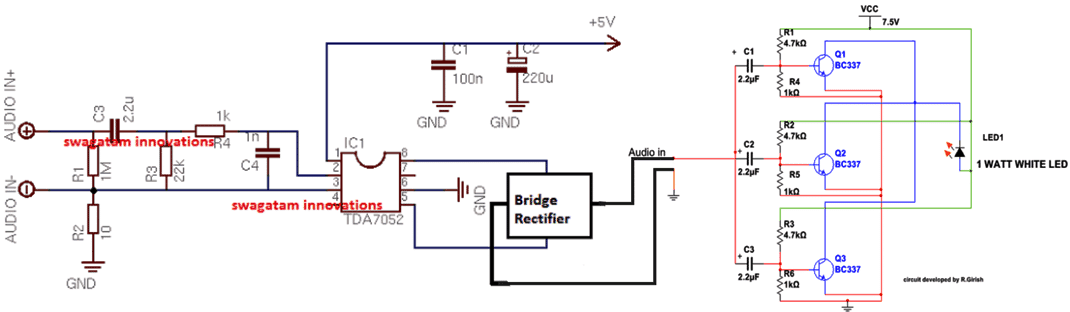 The above design now looks to be a perfect Li-Fi internet transmitter circuit without any flaws.
 Card and keychain type tags:
 As we can see that, a part of the PCB is surrounded by conducting path in square shape on the reader; this will generate electromagnetic field for the tag at 13.56MHz frequency.
The generated EMF is picked by the tag and converts to sufficient voltage for the tag to operate, the tag will sends out the necessary information in pulse form back to the reader.
The on-board microcontroller decodes the information.
As we can see that, a part of the PCB is surrounded by conducting path in square shape on the reader; this will generate electromagnetic field for the tag at 13.56MHz frequency.
The generated EMF is picked by the tag and converts to sufficient voltage for the tag to operate, the tag will sends out the necessary information in pulse form back to the reader.
The on-board microcontroller decodes the information.
 The schematic is very easy and self-explanatory, few jumper wires is enough to accomplish this project.
We are going to power the arduino and RFID via USB port of the computer.
The operating voltage of RC522 is 3.3V, do not connect 5V supply to the module and will damage the on-board components.
The schematic is very easy and self-explanatory, few jumper wires is enough to accomplish this project.
We are going to power the arduino and RFID via USB port of the computer.
The operating voltage of RC522 is 3.3V, do not connect 5V supply to the module and will damage the on-board components.
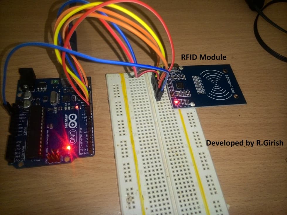 ThatˇŻs all the hardware connections, now letˇŻs jump into coding.
Before uploading the program, download the library file from the following link and move to library folder of arduino IDE.
github.com/miguelbalboa/rfid.git
ThatˇŻs all the hardware connections, now letˇŻs jump into coding.
Before uploading the program, download the library file from the following link and move to library folder of arduino IDE.
github.com/miguelbalboa/rfid.git
 The above set up shows an external PWM motor driver simply configured using some diodes, an opto-coupler and a BJT stage.
The PWM from the Bluetooth Headset is passed through a bridge diode network and then applied at the input of an opto coupler.
The output from the opto coupler is finally fed to a motor driver stage.
Now as the PWM from Bluetooth headset is changed, the motor responds to the PWM and correspondingly changes its speed.
The above set up shows an external PWM motor driver simply configured using some diodes, an opto-coupler and a BJT stage.
The PWM from the Bluetooth Headset is passed through a bridge diode network and then applied at the input of an opto coupler.
The output from the opto coupler is finally fed to a motor driver stage.
Now as the PWM from Bluetooth headset is changed, the motor responds to the PWM and correspondingly changes its speed.
 The PWM transmission for the Bluetooth headset can be obtained from your Android phone.
For this you may have to install any standard PWM generator application and then "pair" it up with your Bluetooth headset.
Next, you would be prompted to adjust the duty cycle, PWM, frequency etc within the application, which you can fix as per your preferences.
Once all these initial set ups are completed, the PWM transmission for the Buetooth headset could be initiated for executing the motor control operations.
The PWM or the frequency could be changed as per your wish and will, from your android phone application whenever the speed of the motor is required to be altered.
This concludes our tutorial on Bluetooth PWM motor controller circuit, which looks extremely simple and useful, thanks to the all latest technology like android applications and Bluetooth features.
The PWM transmission for the Bluetooth headset can be obtained from your Android phone.
For this you may have to install any standard PWM generator application and then "pair" it up with your Bluetooth headset.
Next, you would be prompted to adjust the duty cycle, PWM, frequency etc within the application, which you can fix as per your preferences.
Once all these initial set ups are completed, the PWM transmission for the Buetooth headset could be initiated for executing the motor control operations.
The PWM or the frequency could be changed as per your wish and will, from your android phone application whenever the speed of the motor is required to be altered.
This concludes our tutorial on Bluetooth PWM motor controller circuit, which looks extremely simple and useful, thanks to the all latest technology like android applications and Bluetooth features.

 The door mechanism and the associated electrical can be understood with the following points:
The frame of the door consists of a central "U" shaped latch driven by a 12V solenoid unit.
The Door Solenoid
The door mechanism and the associated electrical can be understood with the following points:
The frame of the door consists of a central "U" shaped latch driven by a 12V solenoid unit.
The Door Solenoid

 The frame can be also seen having a concealed reed relay switch
The movable door lower edge is embedded with a permanent magnet such that while it's in its normal closed condition, the magnet aligns itself exactly face to face with the reed relay.
This concludes the door mechanism electrical, now let's see how this needs to be configured with an electronic circuit for the desired automatic "pet" triggered operation.
The frame can be also seen having a concealed reed relay switch
The movable door lower edge is embedded with a permanent magnet such that while it's in its normal closed condition, the magnet aligns itself exactly face to face with the reed relay.
This concludes the door mechanism electrical, now let's see how this needs to be configured with an electronic circuit for the desired automatic "pet" triggered operation.
 The circuit shown above is a simple delay ON timer circuit using T1, T2, R2, C2 as the main components.
Normally the delay timer is supposed to operate the relay after some delay as soon as the circuit is powered with an input supply of 12V.
However in the shown circuit design, the specified delay operation is controlled by two parameters, 1) the reed switch, and the opto coupler IC (with the attached BC547 transistor).
The circuit shown above is a simple delay ON timer circuit using T1, T2, R2, C2 as the main components.
Normally the delay timer is supposed to operate the relay after some delay as soon as the circuit is powered with an input supply of 12V.
However in the shown circuit design, the specified delay operation is controlled by two parameters, 1) the reed switch, and the opto coupler IC (with the attached BC547 transistor).
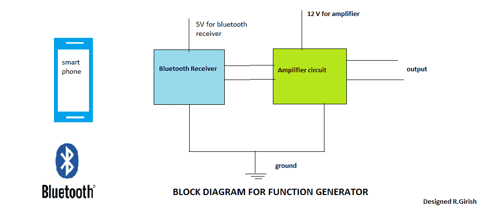
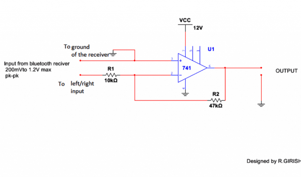
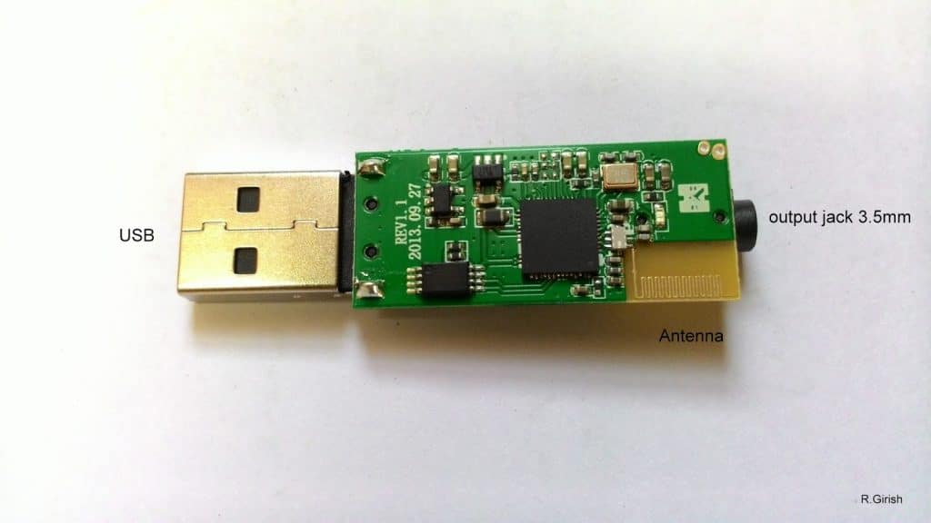 The Bluetooth receiver is an inexpensive device which is commonly available on e-commerce sites or electronics stationary shops.
The above gadget had plastic casing which is removed to show its internals.
It may be powered from USB or you may solder their power rails of the USB to regulated power supply like LM7805.
The Bluetooth receiver is an inexpensive device which is commonly available on e-commerce sites or electronics stationary shops.
The above gadget had plastic casing which is removed to show its internals.
It may be powered from USB or you may solder their power rails of the USB to regulated power supply like LM7805.
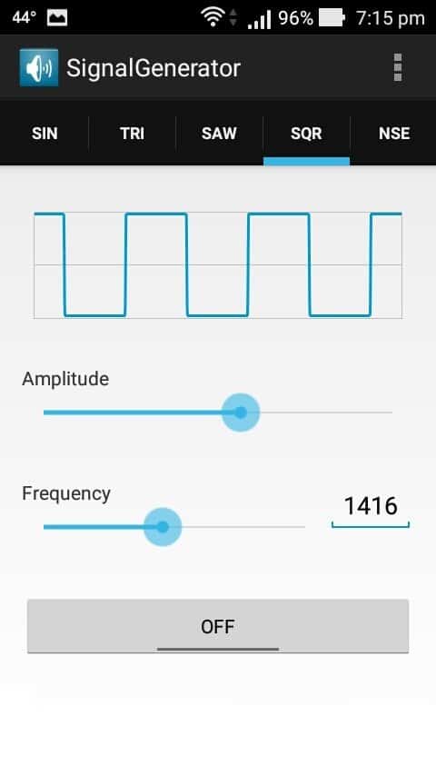
 DIAMETER OF THE COIL IS AROUND 18 CMS
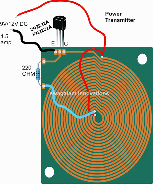 Dimensions: 10 inches by 10 inches, bigger size might enable faster charging and better current output
The figure above shows the power emitter or radiator design, also recall the circuit diagram from our previous post, the above design utilizes exactly the same circuit layout, although here we do it through a PCB by etching the winding layout over it.
A careful observation shows that the above layout has a pair of parallel coiled copper tracks running spirally, and forming the two halves of the transmitter coil, wherein the center tap is acquired with the aid of the linked red jumper wire across the ends of the coils.
The layout allows the design to be compact and effective for the required operations.
The track layout could be in the form of a square, or oval on one side and squarish on the other in order to make the unit even sleeker.
Rest of the portion is quite straightforward and is as per our earlier diagram, where the transistor is 2N2222 included for inducing the required high frequency oscillations and propagation.
The circuit is operated from a 12V/1.5 amp source, and the number of turns (coils) may selected approximately in accordance with the supply voltage value, that is around 15 to 20 turns for each halves of the transmitter coil.
Higher turns will result in lower current and boosted voltage radiations and vice versa
When switched ON, the circuit may be expected to generate a strong magnetic flux around the coiled tracked, equivalent to the input power.
Now the radiated power needs to be absorbed using an identical circuit for executing the wireless power transfer and the intended cell phone charging.
For this we need a power collector or receiver circuit for collecting the radiated power, this may be devised as explained in the following section:
Dimensions: 10 inches by 10 inches, bigger size might enable faster charging and better current output
The figure above shows the power emitter or radiator design, also recall the circuit diagram from our previous post, the above design utilizes exactly the same circuit layout, although here we do it through a PCB by etching the winding layout over it.
A careful observation shows that the above layout has a pair of parallel coiled copper tracks running spirally, and forming the two halves of the transmitter coil, wherein the center tap is acquired with the aid of the linked red jumper wire across the ends of the coils.
The layout allows the design to be compact and effective for the required operations.
The track layout could be in the form of a square, or oval on one side and squarish on the other in order to make the unit even sleeker.
Rest of the portion is quite straightforward and is as per our earlier diagram, where the transistor is 2N2222 included for inducing the required high frequency oscillations and propagation.
The circuit is operated from a 12V/1.5 amp source, and the number of turns (coils) may selected approximately in accordance with the supply voltage value, that is around 15 to 20 turns for each halves of the transmitter coil.
Higher turns will result in lower current and boosted voltage radiations and vice versa
When switched ON, the circuit may be expected to generate a strong magnetic flux around the coiled tracked, equivalent to the input power.
Now the radiated power needs to be absorbed using an identical circuit for executing the wireless power transfer and the intended cell phone charging.
For this we need a power collector or receiver circuit for collecting the radiated power, this may be devised as explained in the following section:
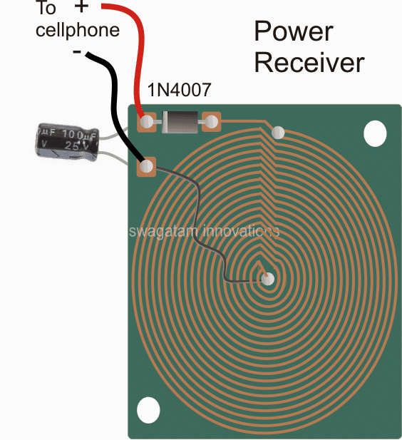 Dimension: 3 inches by 3 inches or as per the accommodation space available inside your cellphone
As may be witnessed in the above receiver design, an identical layout of the coil may seen, except that here the two concentric spirals are connected in parallel to add current in contrast to the transmitter layout which incorporated a series connection owing to the center tap restriction for the design.
The design is supposed to be small enough to fit inside a standard cellphone, just below the hind cover, and the output which is terminated through a diode may be connected either with the battery directly or across the charging socket pins (internally).
Once the above circuits are built, the transmitter circuit may be connected with the indicated DC input, and the receiver module placed right over the transmitter board, at the center.
An LED with a 1k resistor could be included at the output of the receiver circuit in order to get a instant indication of the wireless power conduction process.
After the operation is confirmed, the output from the receiver may be connected to the socket of the cell phone for checking the response of the wireless charging effect.
However before this you may want to confirm the output to the cellphone from the wireless receiver module...it should be around 5 to 6V, if it's more, the black wire could be simply shifted and soldered a few coils towards the top until the right voltage is achieved.
Once all the confirmation are complete the module could be accommodated inside a cellphone and the connections done appropriately.
Finally, hopefully if everything is done correctly the assembly might allow you to keep the cellphone directly over the transmitter set up and enable the proposed wireless cellphone charging to happen successfully.
Dimension: 3 inches by 3 inches or as per the accommodation space available inside your cellphone
As may be witnessed in the above receiver design, an identical layout of the coil may seen, except that here the two concentric spirals are connected in parallel to add current in contrast to the transmitter layout which incorporated a series connection owing to the center tap restriction for the design.
The design is supposed to be small enough to fit inside a standard cellphone, just below the hind cover, and the output which is terminated through a diode may be connected either with the battery directly or across the charging socket pins (internally).
Once the above circuits are built, the transmitter circuit may be connected with the indicated DC input, and the receiver module placed right over the transmitter board, at the center.
An LED with a 1k resistor could be included at the output of the receiver circuit in order to get a instant indication of the wireless power conduction process.
After the operation is confirmed, the output from the receiver may be connected to the socket of the cell phone for checking the response of the wireless charging effect.
However before this you may want to confirm the output to the cellphone from the wireless receiver module...it should be around 5 to 6V, if it's more, the black wire could be simply shifted and soldered a few coils towards the top until the right voltage is achieved.
Once all the confirmation are complete the module could be accommodated inside a cellphone and the connections done appropriately.
Finally, hopefully if everything is done correctly the assembly might allow you to keep the cellphone directly over the transmitter set up and enable the proposed wireless cellphone charging to happen successfully.
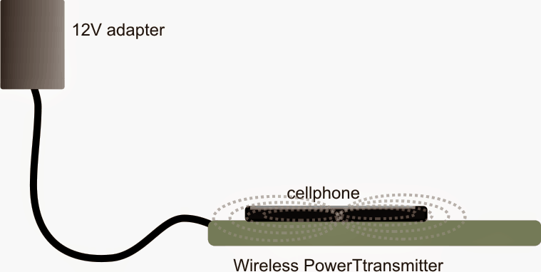
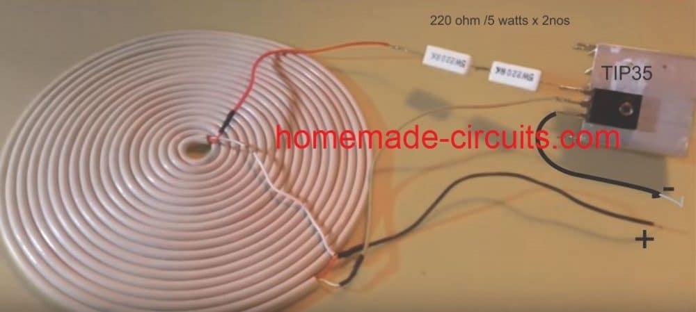
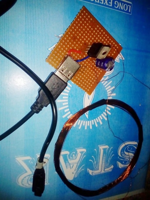
 Image Courtesy:https://www.nxp.com/docs/en/data-sheet/TDA8953.pdf

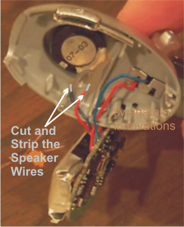
 To break it open you can use a screw driver as shown in the picture below.
However you will need to maintain extreme dexterity and care while operating the gadget making sure you don't damage the internal circuitry.
To break it open you can use a screw driver as shown in the picture below.
However you will need to maintain extreme dexterity and care while operating the gadget making sure you don't damage the internal circuitry.
 Once the cover is removed, you would come across another plastic shielding which you can identically remove using the tip of your screw driver.
 Once the inner protection shield is peeled of, the actual PCB with various components would pop out from the shell as shown below.
 In this position the few important things that would become visible are: two wires running toward a small speaker, two wires towards an in built MIC, an USB connector and an attached battery.
See below for the details
In this position the few important things that would become visible are: two wires running toward a small speaker, two wires towards an in built MIC, an USB connector and an attached battery.
See below for the details

 Once removed....
the MIC, the speaker and the PCB with all the associated components could be studied in details as shown in the following figure:
Once removed....
the MIC, the speaker and the PCB with all the associated components could be studied in details as shown in the following figure:
 Another important area we would be interested within the circuit is the USB socket, since its the input which receives all the data, and also the battery for getting well versed regarding what's inside a typical Bluetooth headset.
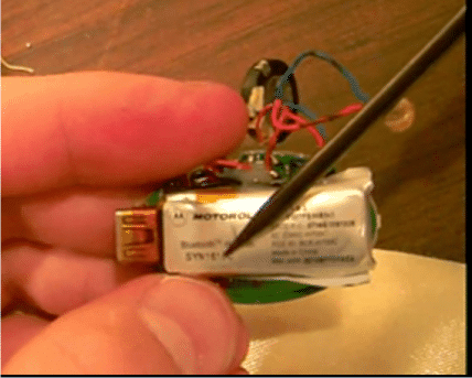 OK that's it, now we exactly know all that's inside a Bluetooth headset gear, and it's time to learn a few of the simple hacking techniques that would enable us to use any Bluetooth headset unit for performing the intended operations.
The next post will explain how to hack a Bluetooth Headset for other personalized implementations such as for remotely operating an appliance, as a spy bug, and audio related applications such as for making wireless speaker systems and home theater systems.
OK that's it, now we exactly know all that's inside a Bluetooth headset gear, and it's time to learn a few of the simple hacking techniques that would enable us to use any Bluetooth headset unit for performing the intended operations.
The next post will explain how to hack a Bluetooth Headset for other personalized implementations such as for remotely operating an appliance, as a spy bug, and audio related applications such as for making wireless speaker systems and home theater systems.
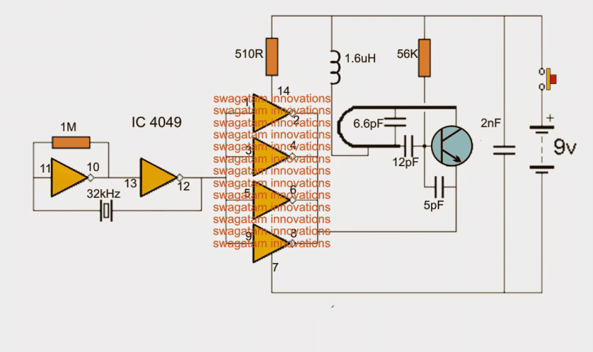 All Transistors are 2N3563, the U shape coil is a single half turn using a 1mm copper wire with 5mm diameter
In case an additional gate is included along with a crystal hooked up between the output as well as the input, a "fight" transpires between the transmission coming from the 1M and the rate of recurrence transferred by the crystal.
Considering that the crystal possesses a reduced impedance as compared to the 1M, it accomplishes a more substantial signal to input pin 11 along with the 2 gates function at the frequency of the crystal.
The precise characteristics of the correct way the reception from the crystal overtakes the signal administered back from the 1M resistor is not critical in spite of this providing you can contemplate the first gate starts out to rise in frequency from nil, every time the signal reaches 32kHz, it commences to initialize the crystal which in turn forces the signal on the reverse side and into the input pin of the first gate.
Each transmitters churn out the identical outcomes, a 303MHz carrier with a 32kHz modulation (frequency - despite the fact that we are unable to perceive sound in this frequency).
Each possess the matching spectrum.
The oscillator coil is furthermore the radiator of the signal as well as the 1.5uH inductor on the "centre tap" of the coil is often as high as 10uH or as little as 1.5uH, with minimal variance in output.
The frequency might well need to be realigned somewhat if the inductor is modified.
We transformed it for a forty turn air-would coil working with.25mm wire on a 2mm former.
This amplified the distance by one metre.
All Transistors are 2N3563, the U shape coil is a single half turn using a 1mm copper wire with 5mm diameter
In case an additional gate is included along with a crystal hooked up between the output as well as the input, a "fight" transpires between the transmission coming from the 1M and the rate of recurrence transferred by the crystal.
Considering that the crystal possesses a reduced impedance as compared to the 1M, it accomplishes a more substantial signal to input pin 11 along with the 2 gates function at the frequency of the crystal.
The precise characteristics of the correct way the reception from the crystal overtakes the signal administered back from the 1M resistor is not critical in spite of this providing you can contemplate the first gate starts out to rise in frequency from nil, every time the signal reaches 32kHz, it commences to initialize the crystal which in turn forces the signal on the reverse side and into the input pin of the first gate.
Each transmitters churn out the identical outcomes, a 303MHz carrier with a 32kHz modulation (frequency - despite the fact that we are unable to perceive sound in this frequency).
Each possess the matching spectrum.
The oscillator coil is furthermore the radiator of the signal as well as the 1.5uH inductor on the "centre tap" of the coil is often as high as 10uH or as little as 1.5uH, with minimal variance in output.
The frequency might well need to be realigned somewhat if the inductor is modified.
We transformed it for a forty turn air-would coil working with.25mm wire on a 2mm former.
This amplified the distance by one metre.
 All Transistors are 2N3563, the antenna coil is 2.5 turns of 1mm copper wire over a 5mm variable slug assembly
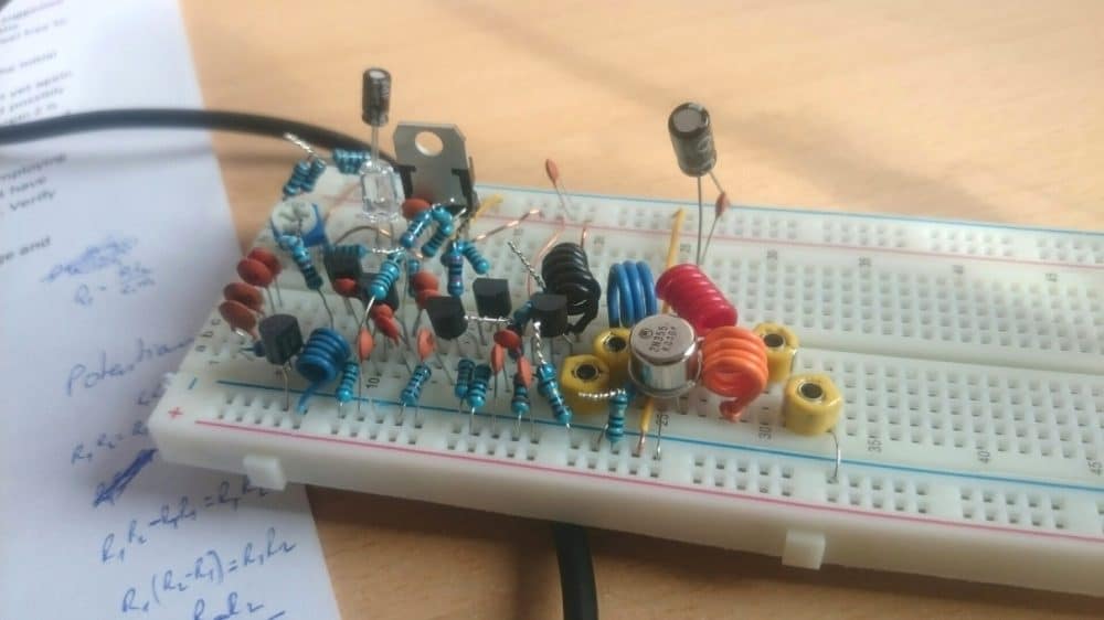
 The device detects the inbound ultrasonic signal and passes it to the base terminal of the transistor Q1. The two-transistor stage using Q1 and Q2 works like a booster amplifier stage which elevates the detected ultrasonic signals to an amount which is enough to trigger the single input of a very unconventional mixer circuit.
The IC U2 which is a quad bilateral switch operates like an exceptionally clean balanced-mixer circuit intended for the superheterodyne receiver.
IC U1a is configured like a variable-frequency squarewave-oscillator circuit.
Resistors R5, R6, and capacitor C4 are configured to fix the frequency and tuning range of the oscillator stage.
The squarewave signal from the oscillator stage is directed across a a couple of tracks.
In one track, the U1a output becomes the input for the pins12 and pin13 of U2. In the second track, the signal goes to the Q3 base, constructed like an inverter.
This inverter generates a signal output which is 180ˇă out of phase with the input signal.
This out of phase signal from of Q3 is then applied to U2 at its pins 5 and 6.
At these pinouts of the op amp the two input signals which are one ultrasonic input originating from MIC1 while the other from the oscillator output are mixed together.
This mixing of the ultrasonic signal from the MIC with the oscillator's square-wave causes the generation of an audible combination which is then applied to the input of a differential amplifier UIb, which is configured to provide a voltage gain of 2.
The U1b output available at pin 7 is subsequently filtered and cleaned by the resistors R19 and C9 to eliminate the high frequency material of the mixed signal.
Since it is only the difference frequency that matters, the sum frequency (the inbound ultrasonic signal added to the oscillator frequency), that may be excessively high for our ear to hear, is eradicated by R19 and C9 to provide a thoroughly clean and filtered output signal.
This cleaned up output is finally supplied to the power amplifier U3. Resistor R21 is configured to work like the circuit's volume control.
The device detects the inbound ultrasonic signal and passes it to the base terminal of the transistor Q1. The two-transistor stage using Q1 and Q2 works like a booster amplifier stage which elevates the detected ultrasonic signals to an amount which is enough to trigger the single input of a very unconventional mixer circuit.
The IC U2 which is a quad bilateral switch operates like an exceptionally clean balanced-mixer circuit intended for the superheterodyne receiver.
IC U1a is configured like a variable-frequency squarewave-oscillator circuit.
Resistors R5, R6, and capacitor C4 are configured to fix the frequency and tuning range of the oscillator stage.
The squarewave signal from the oscillator stage is directed across a a couple of tracks.
In one track, the U1a output becomes the input for the pins12 and pin13 of U2. In the second track, the signal goes to the Q3 base, constructed like an inverter.
This inverter generates a signal output which is 180ˇă out of phase with the input signal.
This out of phase signal from of Q3 is then applied to U2 at its pins 5 and 6.
At these pinouts of the op amp the two input signals which are one ultrasonic input originating from MIC1 while the other from the oscillator output are mixed together.
This mixing of the ultrasonic signal from the MIC with the oscillator's square-wave causes the generation of an audible combination which is then applied to the input of a differential amplifier UIb, which is configured to provide a voltage gain of 2.
The U1b output available at pin 7 is subsequently filtered and cleaned by the resistors R19 and C9 to eliminate the high frequency material of the mixed signal.
Since it is only the difference frequency that matters, the sum frequency (the inbound ultrasonic signal added to the oscillator frequency), that may be excessively high for our ear to hear, is eradicated by R19 and C9 to provide a thoroughly clean and filtered output signal.
This cleaned up output is finally supplied to the power amplifier U3. Resistor R21 is configured to work like the circuit's volume control.
 Figure.1 This simple ultrasonic
generator may be constructed without much difficulty
Figure.1 This simple ultrasonic
generator may be constructed without much difficulty
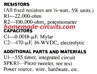 Our very first circuit, is shown in the above Fig, is an ultrasonic generator which uses the well-known 555 IC timer in a adjustable frequency astable multivibrator circuit.
The design outputs a square wave signal which, works with R2, for tuning through around a frequency range of 12 kHz to over 50 kHz.
This frequency range can easily be adjusted by altering the value of capacitor C1; employing a lower value will cause the range to go higher, while larger value will make the range that much smaller.
Our very first circuit, is shown in the above Fig, is an ultrasonic generator which uses the well-known 555 IC timer in a adjustable frequency astable multivibrator circuit.
The design outputs a square wave signal which, works with R2, for tuning through around a frequency range of 12 kHz to over 50 kHz.
This frequency range can easily be adjusted by altering the value of capacitor C1; employing a lower value will cause the range to go higher, while larger value will make the range that much smaller.
 The next ultrasonic generator, revealed in the above Fig.
2, makes use of 6 buffer gates of a solitary 4049 CMOS inverting buffer IC.
A couple of the buffers, U1a and U1b, can be seen attached within a variable-frequency astable-oscillator circuit having a 50 % duty cycle, square wave output.
The rest of the 4 buffers all connected in parallel in order to enhance the output over the connected piezo element.
This much better ultrasonic generator's frequency range is approximately similar to the previous IC 555 version.
However, The major advantage of this design is its accurate 50% duty cycle around the full frequency range.
That said, the frequency range could be made higher by lowering the capacitor C1 value, and the frequency can be decreased by using higher values for C1. The 100k potentiometer, along with resistor R3, fixes the output frequency.
The next ultrasonic generator, revealed in the above Fig.
2, makes use of 6 buffer gates of a solitary 4049 CMOS inverting buffer IC.
A couple of the buffers, U1a and U1b, can be seen attached within a variable-frequency astable-oscillator circuit having a 50 % duty cycle, square wave output.
The rest of the 4 buffers all connected in parallel in order to enhance the output over the connected piezo element.
This much better ultrasonic generator's frequency range is approximately similar to the previous IC 555 version.
However, The major advantage of this design is its accurate 50% duty cycle around the full frequency range.
That said, the frequency range could be made higher by lowering the capacitor C1 value, and the frequency can be decreased by using higher values for C1. The 100k potentiometer, along with resistor R3, fixes the output frequency.
 The LM567 phase-locked-loop (PLL) IC is used for generating ultrasonic frequency in our 3rd concept as proven in the above figure 3. This circuit provides a number of features better than previous two ultrasonic concepts.
First, the IC 567's in-built oscillator is developed to work within a incredibly large frequency spectrum, from under 1 Hz and as high as 500 kHz.
The generator's output waveform, at pin 5, exhibits outstanding symmetry all through its performance range.
The generator additionally gives a increased output compared to other two circuits for the reason that output is matched much closely to the piezo tweeter's (SPKR1) impedance.
The output of the circuit could be tweaked through around 10 kHz to more than 100 kHz working with potentiometer R5. Transistor Q1 is hooked up like a common collector circuit in order to keep the 567's output aloof as well as to drive the output-amplifier circuit which is created using the transistors Q2 and Q3. The circuit could be changed into an ultrasonic cw transmitter by breaking the IC's pin 7 connection and inserting a switch key in series.
In that case, you will require some form of ultrasonic receiver to hear the signals; and that is the exactly what we are going to discuss in our next circuit.
The LM567 phase-locked-loop (PLL) IC is used for generating ultrasonic frequency in our 3rd concept as proven in the above figure 3. This circuit provides a number of features better than previous two ultrasonic concepts.
First, the IC 567's in-built oscillator is developed to work within a incredibly large frequency spectrum, from under 1 Hz and as high as 500 kHz.
The generator's output waveform, at pin 5, exhibits outstanding symmetry all through its performance range.
The generator additionally gives a increased output compared to other two circuits for the reason that output is matched much closely to the piezo tweeter's (SPKR1) impedance.
The output of the circuit could be tweaked through around 10 kHz to more than 100 kHz working with potentiometer R5. Transistor Q1 is hooked up like a common collector circuit in order to keep the 567's output aloof as well as to drive the output-amplifier circuit which is created using the transistors Q2 and Q3. The circuit could be changed into an ultrasonic cw transmitter by breaking the IC's pin 7 connection and inserting a switch key in series.
In that case, you will require some form of ultrasonic receiver to hear the signals; and that is the exactly what we are going to discuss in our next circuit.
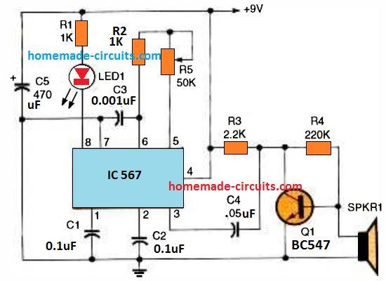 This tunable IC 567 ultrasonic receiver can be paired with the
explained LM 567 ultrasonic transmitter for best results.
A ultrasonic receiver circuit using a 567 PLL IC that features a frequency tuning capability is shown in the above diagram.
The IC's tunable oscillator circuit is identical to the earlier generator circuit, and handles exactly the same range of frequency.
An LED is positioned at the pin 8 detector pin of the IC which quickly indicates the detected signals.
Transistor Q1 is positioned to amplify the minute ultrasonic signals detected by the piezo device and forwards them onto the PLL.
This tunable IC 567 ultrasonic receiver can be paired with the
explained LM 567 ultrasonic transmitter for best results.
A ultrasonic receiver circuit using a 567 PLL IC that features a frequency tuning capability is shown in the above diagram.
The IC's tunable oscillator circuit is identical to the earlier generator circuit, and handles exactly the same range of frequency.
An LED is positioned at the pin 8 detector pin of the IC which quickly indicates the detected signals.
Transistor Q1 is positioned to amplify the minute ultrasonic signals detected by the piezo device and forwards them onto the PLL.
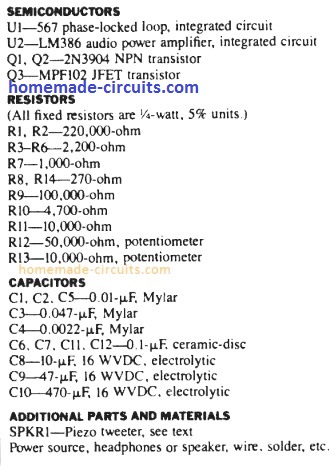 The last ultrasonic receiver circuit design is actually an extremely sensitive ultrasonic receiver which can easily pick up almost anything within the ultrasonic frequency range.
You possibly can listen to insects, bats communications, engines, etc.; the idea could also be used in conjunction with the above explained ultrasonic generators for developing high quality ultrasonic systems.
The design, works using the principle of direct conversion.
Transistors Q1 and Q2 boost the ultrasonic signals detected by the piezo speaker.
The Q2's collector output is then used to drive the JFET (Q3) input, which can be seen hooked up like a product-detector circuit.
The PLL (U1) stage in this concept is employed like a tunable heterodyne oscillator which additionally feeds the input of the JFET detector circuit.
The inbound ultrasonic signal combines with the frequency of the heterodyne-oscillator generating a sum and difference frequency.
The high frequency element is filtered out through the C3, R8, and C6 component network.
The leftover low frequency output is allowed to enter across the LM386 audio amplifier input.
A speaker or headphones could be attached to the circuit's audio output.
The last ultrasonic receiver circuit design is actually an extremely sensitive ultrasonic receiver which can easily pick up almost anything within the ultrasonic frequency range.
You possibly can listen to insects, bats communications, engines, etc.; the idea could also be used in conjunction with the above explained ultrasonic generators for developing high quality ultrasonic systems.
The design, works using the principle of direct conversion.
Transistors Q1 and Q2 boost the ultrasonic signals detected by the piezo speaker.
The Q2's collector output is then used to drive the JFET (Q3) input, which can be seen hooked up like a product-detector circuit.
The PLL (U1) stage in this concept is employed like a tunable heterodyne oscillator which additionally feeds the input of the JFET detector circuit.
The inbound ultrasonic signal combines with the frequency of the heterodyne-oscillator generating a sum and difference frequency.
The high frequency element is filtered out through the C3, R8, and C6 component network.
The leftover low frequency output is allowed to enter across the LM386 audio amplifier input.
A speaker or headphones could be attached to the circuit's audio output.
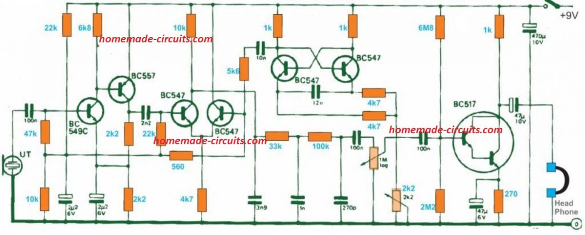 The 'ultrasound' detected by the input transducer is boosted and fed to a product detector.
An astable multivibrator is included since the BFO stability may be not be of much significance.
In addition for the required signal differential, the circuit additionally generates the BFO signal on its own as well as the summing frequency, which is then terminated inside a low pass filter fixed at 4 kHz.
The signal resulting here is yet again amplified to operate a set of headphones.
The circuit works with around 8 milliamps, therefore it can easily be powered from a 9 V dry battery.
The 'ultrasound' detected by the input transducer is boosted and fed to a product detector.
An astable multivibrator is included since the BFO stability may be not be of much significance.
In addition for the required signal differential, the circuit additionally generates the BFO signal on its own as well as the summing frequency, which is then terminated inside a low pass filter fixed at 4 kHz.
The signal resulting here is yet again amplified to operate a set of headphones.
The circuit works with around 8 milliamps, therefore it can easily be powered from a 9 V dry battery.
 The Q2 output gets rectified by the diode D1 and the pin#2 voltage of IC1 turns more negative as the input signal rises.
For input signal that is powerful enough, the amplifier does the job of just clipping the output, which in response to powerful signals generates a square wave jumping across the +/- supply rails.
1C1 works like a comparator and compares the pin#2 voltage, meaning the level of the sound with reference voltage on pin#3. As long as the pin#2 potential is lower than pin 3, meaning in the presence of an input signal, the IC1 output becomes high (approximately 10.5 volts) which triggers ON BJT Q3 which in turn switches ON the relay.
The opposite action happens when pin#2 is at a greater voltage than pin#3. A little quantity of positive feedback is supplied by resistor R9 to generate a little hysteresis which prohibits relay stuttering.
In case the resistor R9 is swapped out with the capacitor C4 the IC1 turns into a monostable which means if the input signal is available only for a brief moment the relay will probably shut off after about a second.
In case the input signal remains for more than 1 second the relay will remain in the open state for the period equivalent to the absence of signal.
The Q2 output gets rectified by the diode D1 and the pin#2 voltage of IC1 turns more negative as the input signal rises.
For input signal that is powerful enough, the amplifier does the job of just clipping the output, which in response to powerful signals generates a square wave jumping across the +/- supply rails.
1C1 works like a comparator and compares the pin#2 voltage, meaning the level of the sound with reference voltage on pin#3. As long as the pin#2 potential is lower than pin 3, meaning in the presence of an input signal, the IC1 output becomes high (approximately 10.5 volts) which triggers ON BJT Q3 which in turn switches ON the relay.
The opposite action happens when pin#2 is at a greater voltage than pin#3. A little quantity of positive feedback is supplied by resistor R9 to generate a little hysteresis which prohibits relay stuttering.
In case the resistor R9 is swapped out with the capacitor C4 the IC1 turns into a monostable which means if the input signal is available only for a brief moment the relay will probably shut off after about a second.
In case the input signal remains for more than 1 second the relay will remain in the open state for the period equivalent to the absence of signal.


 In this post we are going to construct a ultrasonic based solar powered wireless water level indicator using Arduino in which the Arduinos would be transmitting and receiving at 2.4 GHz wireless frequency.
We will be detecting the water level in the tank using ultrasonics instead of traditional electrode method.
In this post we are going to construct a ultrasonic based solar powered wireless water level indicator using Arduino in which the Arduinos would be transmitting and receiving at 2.4 GHz wireless frequency.
We will be detecting the water level in the tank using ultrasonics instead of traditional electrode method.
 Now measure the full height of the tank from bottom to lid, write it down in meters.
Now measure the height of water holding capacity of tank as shown in the above image and write in down in meters.
You need to enter these two values in the code.
Now measure the full height of the tank from bottom to lid, write it down in meters.
Now measure the height of water holding capacity of tank as shown in the above image and write in down in meters.
You need to enter these two values in the code.
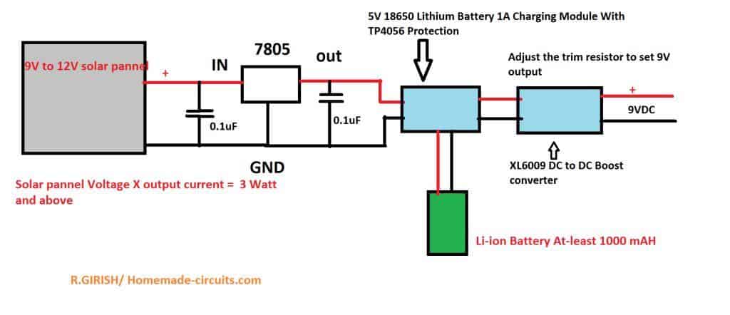 Make sure that your solar panelˇŻs output power i.e.
output (volt x current) is greater than 3 watts.
The solar panel should be 9V to 12V.
12V and 300mA panel is recommended which you can find easily on market.
Battery should be around 3.7V 1000 mAh.
Make sure that your solar panelˇŻs output power i.e.
output (volt x current) is greater than 3 watts.
The solar panel should be 9V to 12V.
12V and 300mA panel is recommended which you can find easily on market.
Battery should be around 3.7V 1000 mAh.
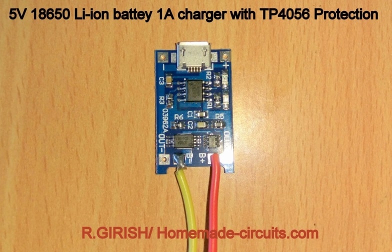 The input can be USB (not used) or external 5V from LM7805 IC.
Make sure that you get the correct module as shown above, it should have TP4056 protection, which has low battery cut-off and short circuit protection.
The output of this should to be fed to XL6009ˇŻs input which will boost to higher voltage, using a small screw driver output of XL6009 should be adjusted to 9V for Arduino.
The input can be USB (not used) or external 5V from LM7805 IC.
Make sure that you get the correct module as shown above, it should have TP4056 protection, which has low battery cut-off and short circuit protection.
The output of this should to be fed to XL6009ˇŻs input which will boost to higher voltage, using a small screw driver output of XL6009 should be adjusted to 9V for Arduino.
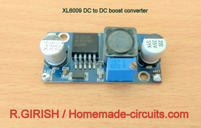 That concludes the transmitterˇŻs hardware.
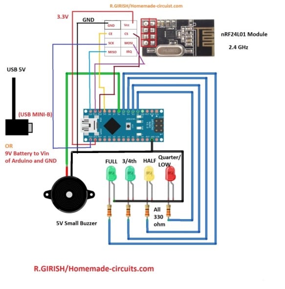 The receiver can show 5 levels.
Alarm, when the tank reached absolute maximum water holding capacity while filling tank.
100 to 75 % - All four LEDs will glow, 75 to 50 % three LEDs will glow, 50 to 25 % two LEDs will glow, 25% and less one LED will glow.
The receiver can be powered from 9V battery or from smartphone charger to USB mini-B cable.
The receiver can show 5 levels.
Alarm, when the tank reached absolute maximum water holding capacity while filling tank.
100 to 75 % - All four LEDs will glow, 75 to 50 % three LEDs will glow, 50 to 25 % two LEDs will glow, 25% and less one LED will glow.
The receiver can be powered from 9V battery or from smartphone charger to USB mini-B cable.
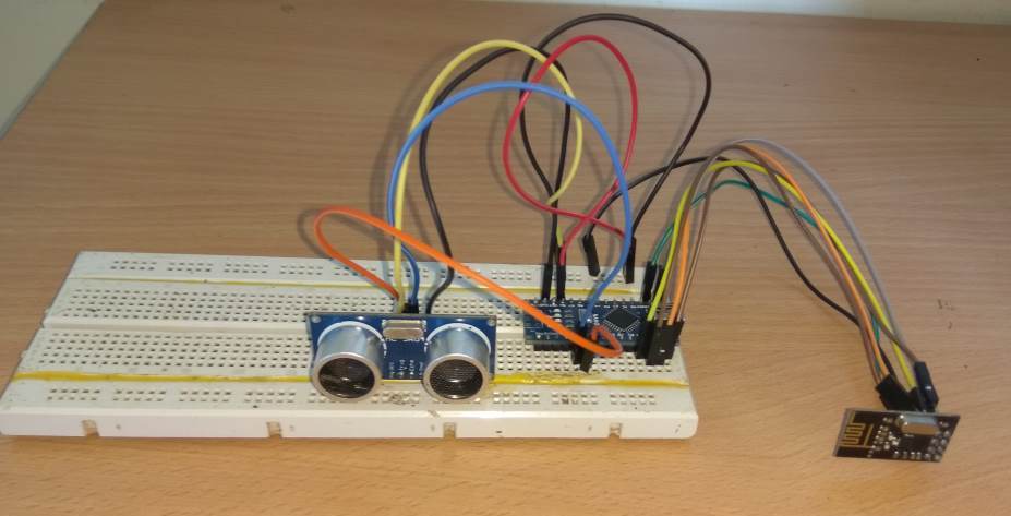 Receiver:
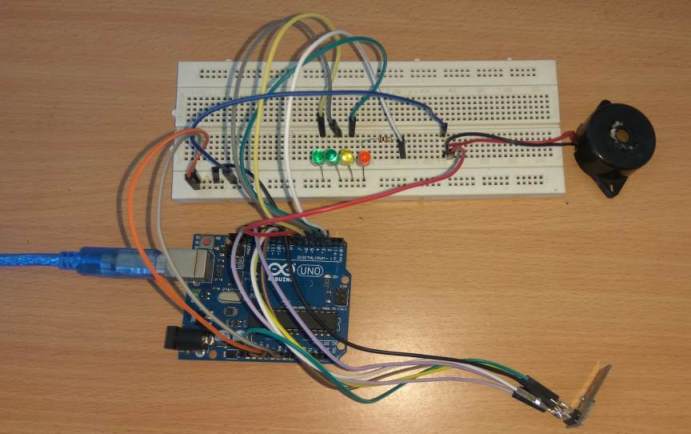 If you have any questions regarding this solar powered ultrasonic wireless water level controller circuit, please feel free to express in the comment, you can expect to get a quick reply.
 The PWM output from the monostable is relative to the capacitance of the RC timing circuit consisting of R4 and the adjustable capacitance of the fluid/conductor capacitance C5, which is directly proportional to the total area of the conductor dipped inside the liquid.
The other 1/2 of the IC 556 timer is configured like a clock operating at 22 kHz that delivers the trigger pulses to the monostable.
Depending on the level of the fluid inside the tank, the capacitance of the "C5" probe varies, which in turn causes the monostable timing to vary.
The varying monostable output from IC is fed to a moving coil ammeter which converts the varying pulses into a meter reading that directly proportional to the the fluid level inside the tank.
A graphite rod removed from your old lantern battery can also used as the ground probe in a situation when the tank is made up of a non-conductive material.
Potentiometer R6, a 5K unit, can be used for calibration of the meter's range.
The PWM output from the monostable is relative to the capacitance of the RC timing circuit consisting of R4 and the adjustable capacitance of the fluid/conductor capacitance C5, which is directly proportional to the total area of the conductor dipped inside the liquid.
The other 1/2 of the IC 556 timer is configured like a clock operating at 22 kHz that delivers the trigger pulses to the monostable.
Depending on the level of the fluid inside the tank, the capacitance of the "C5" probe varies, which in turn causes the monostable timing to vary.
The varying monostable output from IC is fed to a moving coil ammeter which converts the varying pulses into a meter reading that directly proportional to the the fluid level inside the tank.
A graphite rod removed from your old lantern battery can also used as the ground probe in a situation when the tank is made up of a non-conductive material.
Potentiometer R6, a 5K unit, can be used for calibration of the meter's range.
 It is actually a simple electro-mechanical device which connects an internal electrical contact when the water pressure at its pressure nozzle exceeds a preset point.
The internal contacts release or open when the pressure decreases below another specified lower preset point.
It is actually a simple electro-mechanical device which connects an internal electrical contact when the water pressure at its pressure nozzle exceeds a preset point.
The internal contacts release or open when the pressure decreases below another specified lower preset point.
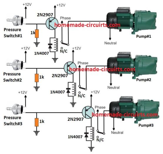 Referring to the diagram, we can see 3 identical stages wherein 3 pressure switches are configured with 3 associated relay driver stages, and the relay contacts attached with the respective 3 water pumps.
In the relay driver stage we have used a PNP transistor because the pressure switch response is normally switched OFF during low pressure and ON when the pressure reaches the maximum threshold level.
This implies that, when pressure is low the internal switch of the pressure device stays unconnected or OFF.
This allows the pnp transistor to switch ON via the ground bias 1 k resistor.
The relay also switches ON and initiates the motor.
This basic operation is same for all the 3 motor pump stages.
Now, as per the requirement, let's assume the pressure is very low, which causes all the 3 pressure switches to disconnect its internal contacts.
As a result all the 3 motor pumps switch ON together.
Due to this the water supply pressure quickly climbs and reaches the desired optimal point, which causes the pressure switch 3 and pressure 2 to switch ON.
This consequently switches OFF the attached motor pump number 3 and 2.
At this point only motor 1 handles the water supply to apartment.
In case the water demand in the building suddenly increases, causes the water pressure to drop so that motor pump #1 alone becomes insufficient to fulfill the need.
The situation triggers pressure switch #2 into action, which initiates motor pump #2 for aiding the required high water pressure demand.
However, in case the water usage keeps rising and the demand is still not fulfilled by the first 2 pumps, pressure switch 3 detects this and activates motor pump #3.
The above sequential switch ON/OFF of the water pumps in response to water tank pressure variations satisfies the main basic requirement.
Referring to the diagram, we can see 3 identical stages wherein 3 pressure switches are configured with 3 associated relay driver stages, and the relay contacts attached with the respective 3 water pumps.
In the relay driver stage we have used a PNP transistor because the pressure switch response is normally switched OFF during low pressure and ON when the pressure reaches the maximum threshold level.
This implies that, when pressure is low the internal switch of the pressure device stays unconnected or OFF.
This allows the pnp transistor to switch ON via the ground bias 1 k resistor.
The relay also switches ON and initiates the motor.
This basic operation is same for all the 3 motor pump stages.
Now, as per the requirement, let's assume the pressure is very low, which causes all the 3 pressure switches to disconnect its internal contacts.
As a result all the 3 motor pumps switch ON together.
Due to this the water supply pressure quickly climbs and reaches the desired optimal point, which causes the pressure switch 3 and pressure 2 to switch ON.
This consequently switches OFF the attached motor pump number 3 and 2.
At this point only motor 1 handles the water supply to apartment.
In case the water demand in the building suddenly increases, causes the water pressure to drop so that motor pump #1 alone becomes insufficient to fulfill the need.
The situation triggers pressure switch #2 into action, which initiates motor pump #2 for aiding the required high water pressure demand.
However, in case the water usage keeps rising and the demand is still not fulfilled by the first 2 pumps, pressure switch 3 detects this and activates motor pump #3.
The above sequential switch ON/OFF of the water pumps in response to water tank pressure variations satisfies the main basic requirement.
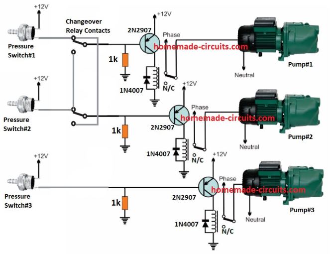 The above diagram demonstrates how this can be done through a simple changeover DPDT relay connected between the relevant pressure switches and the relay driver stages.
In this concept only two motors are considered for the changeover, the third motor is not included to avoid complexity of the design Moreover, two motor sharing seems to be quite enough to keep their wear and tear below the unsafe level.
The changeover relay does one basic job.
It alternately toggles the motor #1 and motor #2 relay drivers across pressure switch #1 and #2. The time for which each motor is kept engaged for the pressurized water supply is determined by a simple IC 4060 timer as circuit as presented below:
The above diagram demonstrates how this can be done through a simple changeover DPDT relay connected between the relevant pressure switches and the relay driver stages.
In this concept only two motors are considered for the changeover, the third motor is not included to avoid complexity of the design Moreover, two motor sharing seems to be quite enough to keep their wear and tear below the unsafe level.
The changeover relay does one basic job.
It alternately toggles the motor #1 and motor #2 relay drivers across pressure switch #1 and #2. The time for which each motor is kept engaged for the pressurized water supply is determined by a simple IC 4060 timer as circuit as presented below:
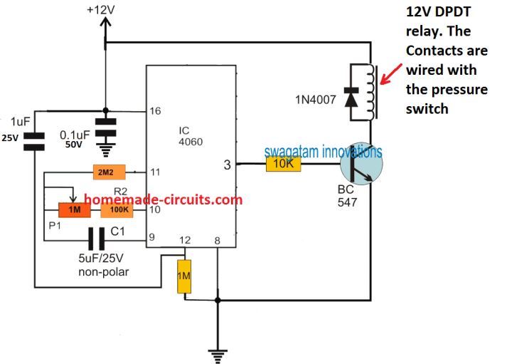 The time delay after which the changeover is initiated can be set by adjusting the 1 M pot appropriately.
With some trial and error the pot resistance can be replaced with a fixed value resistor.
The power supply for all the electronic stages can be obtained from a standard 12 V 1 amp adapter.
All the relays are 12 V 30 amp relays.
The time delay after which the changeover is initiated can be set by adjusting the 1 M pot appropriately.
With some trial and error the pot resistance can be replaced with a fixed value resistor.
The power supply for all the electronic stages can be obtained from a standard 12 V 1 amp adapter.
All the relays are 12 V 30 amp relays.
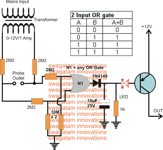
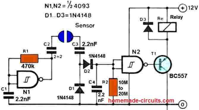 The level sensor's fundamental workingis relatively basic.
An oscillator is formed by the circuit that surrounds N1. C4 will be charged up through the AC coupling capacitors (C2 and C3) and the diodes as soon asthe two sensors are submerged in water, and the output of N2 would be pulled low so thatthe relay will be activatedafter a brief period.
As anexample, the relay could be used to activate a pump, which then regulates the liquid level.
Once conductive link acrossthe two sensors leads is removed, C4 discharges through R2, causing N2's output to become high and the relay to turn off.
The level sensor's fundamental workingis relatively basic.
An oscillator is formed by the circuit that surrounds N1. C4 will be charged up through the AC coupling capacitors (C2 and C3) and the diodes as soon asthe two sensors are submerged in water, and the output of N2 would be pulled low so thatthe relay will be activatedafter a brief period.
As anexample, the relay could be used to activate a pump, which then regulates the liquid level.
Once conductive link acrossthe two sensors leads is removed, C4 discharges through R2, causing N2's output to become high and the relay to turn off.
 NOTE: Please connect a 100K resistor between base/collector of BC557 transistor, otherwise it will not respond to the base 100 Hz switching
In the diagram we can see that the reference ground terminal at the bottom of the tank is supplied with an alternating +/- 6V instead of a normal DC.
This forces the other terminals to conduct in a push-pull manner with the reference to this base terminal and this hopefully prevent corrosion from developing across the connected water level sensing terminals.
NOTE: Please connect a 100K resistor between base/collector of BC557 transistor, otherwise it will not respond to the base 100 Hz switching
In the diagram we can see that the reference ground terminal at the bottom of the tank is supplied with an alternating +/- 6V instead of a normal DC.
This forces the other terminals to conduct in a push-pull manner with the reference to this base terminal and this hopefully prevent corrosion from developing across the connected water level sensing terminals.
 As can be seen the probes are applied with a 12 V AC through the LED of an opto-coupler, and a reverse diode.
One half AC cycles pass through the water and the probes by means of the opto LED, which triggers the controller circuit, while the other half AC cycle flows through the reverse diode.
The continuously reversing cycles of the AC ensures that no electrolysis of water is able to happen across the probes, which prevents any form of oxidation or corrosion development over the probes.
As can be seen the probes are applied with a 12 V AC through the LED of an opto-coupler, and a reverse diode.
One half AC cycles pass through the water and the probes by means of the opto LED, which triggers the controller circuit, while the other half AC cycle flows through the reverse diode.
The continuously reversing cycles of the AC ensures that no electrolysis of water is able to happen across the probes, which prevents any form of oxidation or corrosion development over the probes.

 The idea is quite simple, the two relays control the two valves individually whenever the associated transistor drivers are triggered through the relevant water supply sources.
The upper left transistor's base sensor points are supposed to be attached with the municipal water pipe and this transistor relay stage becomes the preferred controller of the water supply to the overhead tank.
Anytime while the municipal water supply is active, this transistor relay stays activated, making sure that the valve#2 is opened and the municipal water is allowed to fill the overhead tank.
As long as the municipal water supply is present, the upper right side transistor relay stage is rendered inactive by the grounding of its base through the left transistor's collector.
In an event when the municipal water supply is absent, and the borewell water is present, the upper right transistor relay stage becomes active and switches ON the valve#1 enabling the pump to suck the borewell water into the associated tank.
During this time if suppose the municipal water is released, as explained earlier, the valve#1 relay is instantly deactivated by the valve#2 relay transistor, allowing the municipal water to enter the overhead tank instead of the borewell water.
The two BC547 transistors arranged in Darlington pair are used for sensing the over flow situation of the relevant tanks, whether it's the overhead tank or the underground tank, the BC547 pair instantly switches ON and grounds the base signals of the relay driver transistors, disabling the relays and the attached valves, so that the pump motor is switched OFF, and the tanks are prevented from overflowing.
The sensors could be constructed using a pair of brass rods appropriately tinned with solder and cleaned with sand paper and acetone.
The distance between the sensor leads should not be more than 2cms, and should be nicely clamped over a non-conductive base
The sensors can be seen applied separately with a 24V positive to ensure an effective conduction of current across the sensor leads even in the presence of flowing water.
The idea is quite simple, the two relays control the two valves individually whenever the associated transistor drivers are triggered through the relevant water supply sources.
The upper left transistor's base sensor points are supposed to be attached with the municipal water pipe and this transistor relay stage becomes the preferred controller of the water supply to the overhead tank.
Anytime while the municipal water supply is active, this transistor relay stays activated, making sure that the valve#2 is opened and the municipal water is allowed to fill the overhead tank.
As long as the municipal water supply is present, the upper right side transistor relay stage is rendered inactive by the grounding of its base through the left transistor's collector.
In an event when the municipal water supply is absent, and the borewell water is present, the upper right transistor relay stage becomes active and switches ON the valve#1 enabling the pump to suck the borewell water into the associated tank.
During this time if suppose the municipal water is released, as explained earlier, the valve#1 relay is instantly deactivated by the valve#2 relay transistor, allowing the municipal water to enter the overhead tank instead of the borewell water.
The two BC547 transistors arranged in Darlington pair are used for sensing the over flow situation of the relevant tanks, whether it's the overhead tank or the underground tank, the BC547 pair instantly switches ON and grounds the base signals of the relay driver transistors, disabling the relays and the attached valves, so that the pump motor is switched OFF, and the tanks are prevented from overflowing.
The sensors could be constructed using a pair of brass rods appropriately tinned with solder and cleaned with sand paper and acetone.
The distance between the sensor leads should not be more than 2cms, and should be nicely clamped over a non-conductive base
The sensors can be seen applied separately with a 24V positive to ensure an effective conduction of current across the sensor leads even in the presence of flowing water.
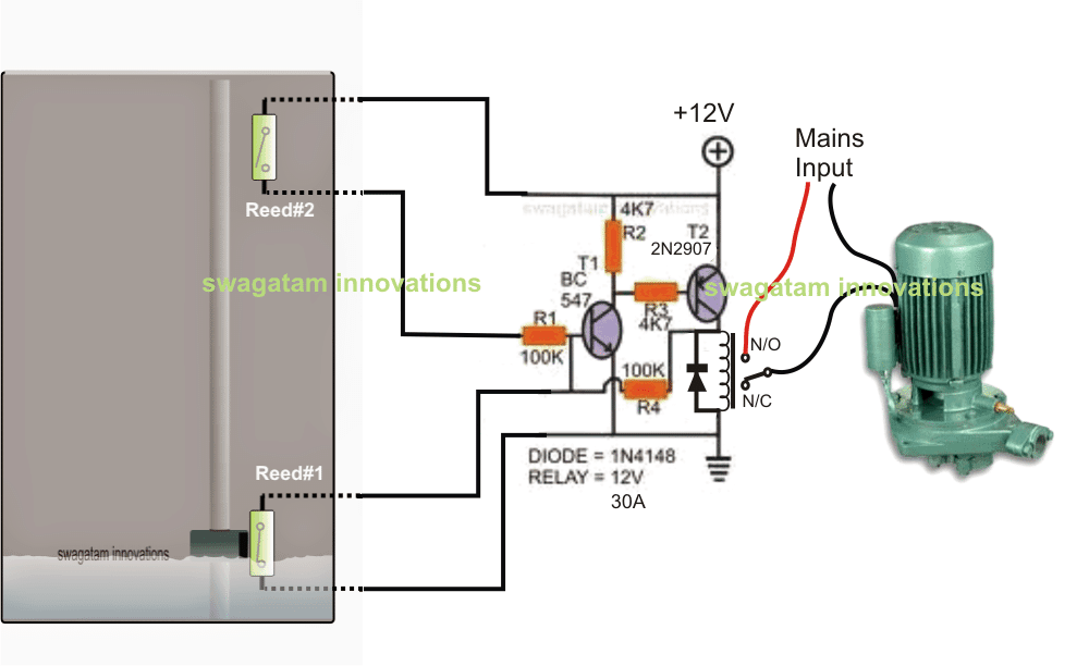
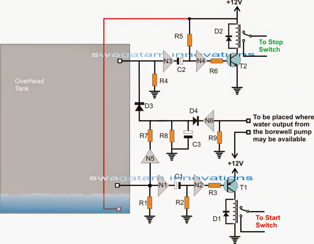 A single IC 4049 can be seen engaged for the entire sensing, start stop actions and the dry run protection execution.
The gates involved here are 6 NOT gates from the IC 4049 which are basically rigged as inverters (for inverting the polarity of the fed voltage at its input).
Let's assume the water inside the over head tank goes below the desired lower threshold, as indicated in the above diagram.
The situation removes the positive potential that ws supplied through the water to the input of N1. N1 responds to this by causing a positive to appear at its output pin, which instantly causes C1 to begin charging via R2.
The above condition also allows the positive from the output of N1 to reach the input of N2, which in turn produces a low or a negative at the base of T1 via R3....the associated relay now toggles ON and activates the "START" button of the contactor....however the relay activation is sustained only for a second or so until C1 is fully charged, this length may be set by appropriately tweaking the values of C1/R2.
For the moment let's forget about N5/N6 stage which are positioned for the dry run protection implementation.
Let's assume the pump is running and pouring water into the shown OH tank.
The water now begins filling inside the tank, until the level reaches the brim of the tank "kissing" the sensor corresponding to the N3 input.
This allow a positive through the water to feed the input of N3, enabling its output to go low (negative), which instantly causes C2 to begin charging via R5, but in the process the input of N4 also becomes low and its output inverts to a high prompting the relay driver to activate the relay.
The upper relay instantly activates but only for a second, toggling the "STOP" button of the contactor, and halting the pump motor.
The relay timing may be set by appropriately tweaking the values of C2/R5.
The above explanation takes care of the automatic water level control by toggling the submersible start/stop button through the circuit's relays.
Now it may be interesting to learn how the dry run protection is designed to prevent a dry run hazard in the absence of water inside the borewell or a underground tank.
Let's go back to the initial situation when the water in the OHT has fallen below the lower threshold and rendered a low at the input of N1....which also renders a low at the input N5.
N5 output turns high due to this and provides a positive supply for C3 so that it can begin charging.
However since the process is also supposed to start the motor, if water is present, the pump may start pouring water in the OHT which is supposed to be detected by the input of N6, causing its output to go low.
With N6 output at low, C3 is inhibited from charging, and the situation stays stalemate...and the motor continues to pump water with no change in the previously explained procedures.
But, suppose the motor experiences a dry run due to an absence of water in the well....as stated above C3 begins charging and the output of N6 never turns negative to stop C3 from charging fully....therefore C3 is able to complete its charging within a predetermined span of time (decided by C3/R8) and finally producing a high (positive) at the input N3.
N3 responds to this in the same way as it would do when the water in the tank is detected at the uppermost threshold....prompting the switching of the upper relay and stopping the motor from running any further.
The dry run protection for the discussed submersible pump start, stop circuit is thus executed.
A single IC 4049 can be seen engaged for the entire sensing, start stop actions and the dry run protection execution.
The gates involved here are 6 NOT gates from the IC 4049 which are basically rigged as inverters (for inverting the polarity of the fed voltage at its input).
Let's assume the water inside the over head tank goes below the desired lower threshold, as indicated in the above diagram.
The situation removes the positive potential that ws supplied through the water to the input of N1. N1 responds to this by causing a positive to appear at its output pin, which instantly causes C1 to begin charging via R2.
The above condition also allows the positive from the output of N1 to reach the input of N2, which in turn produces a low or a negative at the base of T1 via R3....the associated relay now toggles ON and activates the "START" button of the contactor....however the relay activation is sustained only for a second or so until C1 is fully charged, this length may be set by appropriately tweaking the values of C1/R2.
For the moment let's forget about N5/N6 stage which are positioned for the dry run protection implementation.
Let's assume the pump is running and pouring water into the shown OH tank.
The water now begins filling inside the tank, until the level reaches the brim of the tank "kissing" the sensor corresponding to the N3 input.
This allow a positive through the water to feed the input of N3, enabling its output to go low (negative), which instantly causes C2 to begin charging via R5, but in the process the input of N4 also becomes low and its output inverts to a high prompting the relay driver to activate the relay.
The upper relay instantly activates but only for a second, toggling the "STOP" button of the contactor, and halting the pump motor.
The relay timing may be set by appropriately tweaking the values of C2/R5.
The above explanation takes care of the automatic water level control by toggling the submersible start/stop button through the circuit's relays.
Now it may be interesting to learn how the dry run protection is designed to prevent a dry run hazard in the absence of water inside the borewell or a underground tank.
Let's go back to the initial situation when the water in the OHT has fallen below the lower threshold and rendered a low at the input of N1....which also renders a low at the input N5.
N5 output turns high due to this and provides a positive supply for C3 so that it can begin charging.
However since the process is also supposed to start the motor, if water is present, the pump may start pouring water in the OHT which is supposed to be detected by the input of N6, causing its output to go low.
With N6 output at low, C3 is inhibited from charging, and the situation stays stalemate...and the motor continues to pump water with no change in the previously explained procedures.
But, suppose the motor experiences a dry run due to an absence of water in the well....as stated above C3 begins charging and the output of N6 never turns negative to stop C3 from charging fully....therefore C3 is able to complete its charging within a predetermined span of time (decided by C3/R8) and finally producing a high (positive) at the input N3.
N3 responds to this in the same way as it would do when the water in the tank is detected at the uppermost threshold....prompting the switching of the upper relay and stopping the motor from running any further.
The dry run protection for the discussed submersible pump start, stop circuit is thus executed.
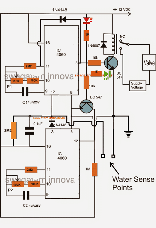
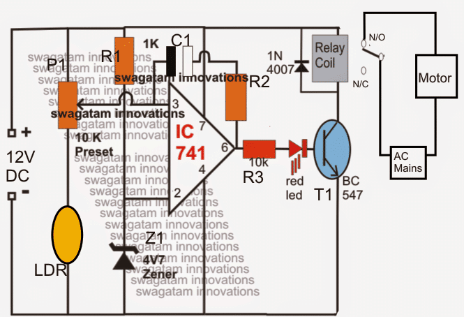 As long as there's an absence of water across the sensing zone, the LDRs experience the incident light (positioned from the opposite side, inside the tank) which in turn keeps pin3 of the IC low, however when water starts rising and tends to cover the LDR in the path, reverts to a high at pin3 of the IC which instantly prompts the opamp output to go high activating the relay and the pump.
A hysteresis control feedback resistor across the opamps (R2/C1)) make sure that the once the situation is sensed it stays latched for some predetermined time and the pump motor is allowed to run until the water has reached the bottom of the tank.
The time for which the opamp stays latched may be determined by adjusting the feedback resistor connected between the output and the input pins of the opamp.
As long as there's an absence of water across the sensing zone, the LDRs experience the incident light (positioned from the opposite side, inside the tank) which in turn keeps pin3 of the IC low, however when water starts rising and tends to cover the LDR in the path, reverts to a high at pin3 of the IC which instantly prompts the opamp output to go high activating the relay and the pump.
A hysteresis control feedback resistor across the opamps (R2/C1)) make sure that the once the situation is sensed it stays latched for some predetermined time and the pump motor is allowed to run until the water has reached the bottom of the tank.
The time for which the opamp stays latched may be determined by adjusting the feedback resistor connected between the output and the input pins of the opamp.
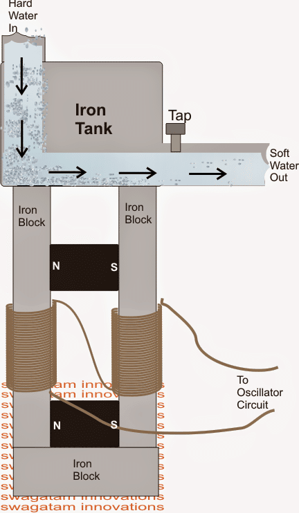
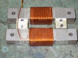
 The shown outputs provides a direct readable data in the form of millivolts which could be used for for triggering an external electronic circuit stage.
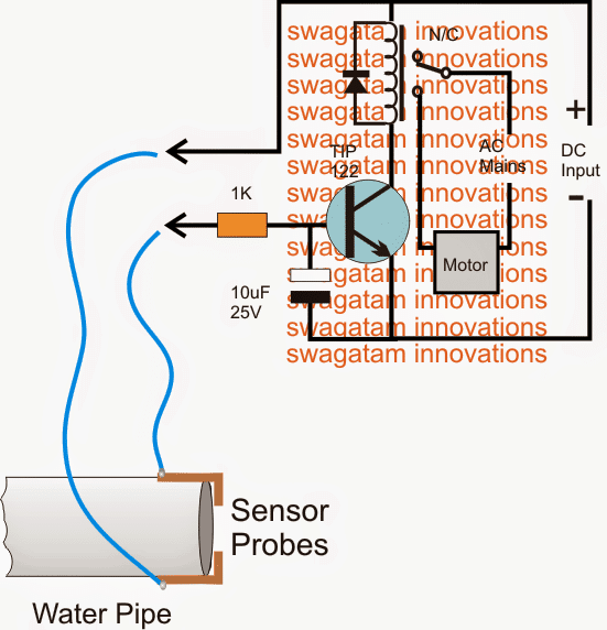 Parts List
Resistor 1k, 1/4 watt, 5% CFR = 1 no
Capacitor 10uF/25V Electrolytic = 1 no
Transistor TIP122 = 1no
Relay 12V/30 Amp/ SPDT = 1no
Diode 1N4007 = 1no
Stainless steel metal for the probes
220 V AC to 12 V DC adapter = 1no
Parts List
Resistor 1k, 1/4 watt, 5% CFR = 1 no
Capacitor 10uF/25V Electrolytic = 1 no
Transistor TIP122 = 1no
Relay 12V/30 Amp/ SPDT = 1no
Diode 1N4007 = 1no
Stainless steel metal for the probes
220 V AC to 12 V DC adapter = 1no
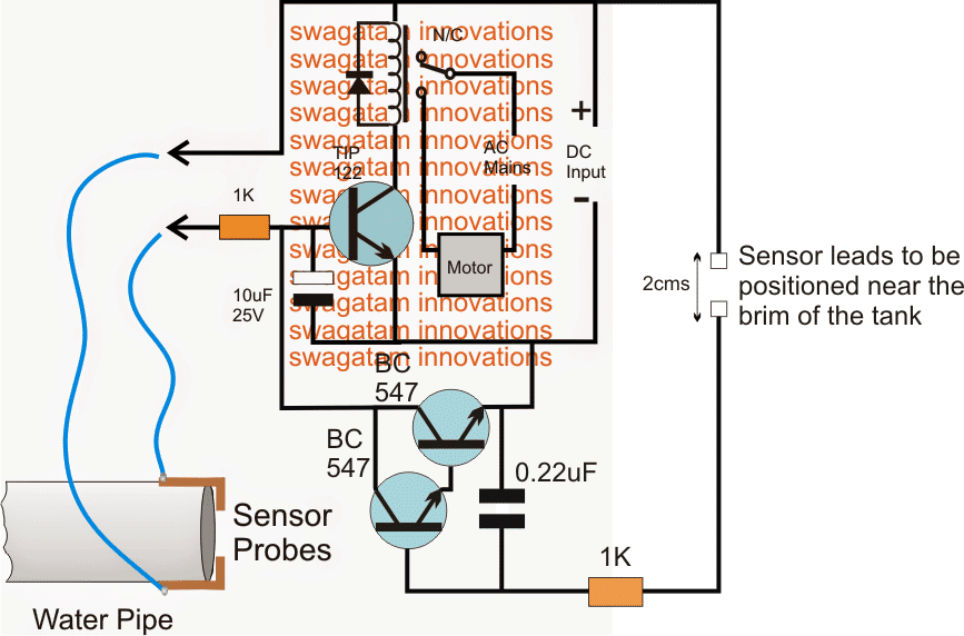 Parts List
Resistor 1k, 1/4 watt, 5% CFR = 2 no
Capacitor 10uF/25V Electrolytic = 1 no
Capacitor 0.22uF PPC = 1no
Transistor TIP122 = 1no
Transistor BC547 = 2nos
Relay 12V/30 Amp/ SPDT = 1no
Diode 1N4007 = 1no
Stainless steel metal for the probes
220 V AC to 12 V DC adapter = 1no
Parts List
Resistor 1k, 1/4 watt, 5% CFR = 2 no
Capacitor 10uF/25V Electrolytic = 1 no
Capacitor 0.22uF PPC = 1no
Transistor TIP122 = 1no
Transistor BC547 = 2nos
Relay 12V/30 Amp/ SPDT = 1no
Diode 1N4007 = 1no
Stainless steel metal for the probes
220 V AC to 12 V DC adapter = 1no
 The pump typically runs at 0.15 to 0.25 amps and 4.5 to 6 volts.
The data above provides the maximum operating conditions.
One end of the pump has a circuit board.
I've attached a very rough picture.
Ultimately,
I'd like the manufacture to modify the circuit board to include the dry run protection.
We need a very small circuit designed that would sense a change in current when the water level is below the pump.
Note that the pump is very small, and the circuit would need to be integrated into the existing board.
Would you be able to design a circuit for this application? If so, how much would you charge?
Cheers,
Ken Adler
President
Eagle Design
The pump typically runs at 0.15 to 0.25 amps and 4.5 to 6 volts.
The data above provides the maximum operating conditions.
One end of the pump has a circuit board.
I've attached a very rough picture.
Ultimately,
I'd like the manufacture to modify the circuit board to include the dry run protection.
We need a very small circuit designed that would sense a change in current when the water level is below the pump.
Note that the pump is very small, and the circuit would need to be integrated into the existing board.
Would you be able to design a circuit for this application? If so, how much would you charge?
Cheers,
Ken Adler
President
Eagle Design
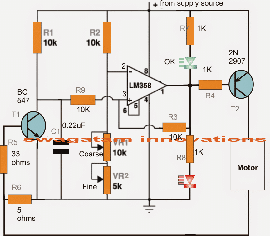
 We use the above explained reed switch in the pipe for detecting the water level conditions via the magnetic ring float either for activating its contacts or vice versa.
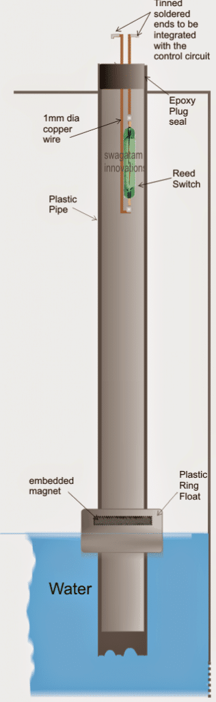 Making the plastic float could be a little complex, as it will require a thick plastic piece to be fabricated such that it consists a hole which is just enough to the pass the plastic pipe smoothly and freely through it.
The upper/inner rim of this plastic float must allow a magnet insertion, this could be done either by drilling a vertical hole through it and snug fit a rod shaped magnet, or make a U shape slot over the upper surface of the float and embed an identically dimensioned U shaped magnet over it.
Making the plastic float could be a little complex, as it will require a thick plastic piece to be fabricated such that it consists a hole which is just enough to the pass the plastic pipe smoothly and freely through it.
The upper/inner rim of this plastic float must allow a magnet insertion, this could be done either by drilling a vertical hole through it and snug fit a rod shaped magnet, or make a U shape slot over the upper surface of the float and embed an identically dimensioned U shaped magnet over it.


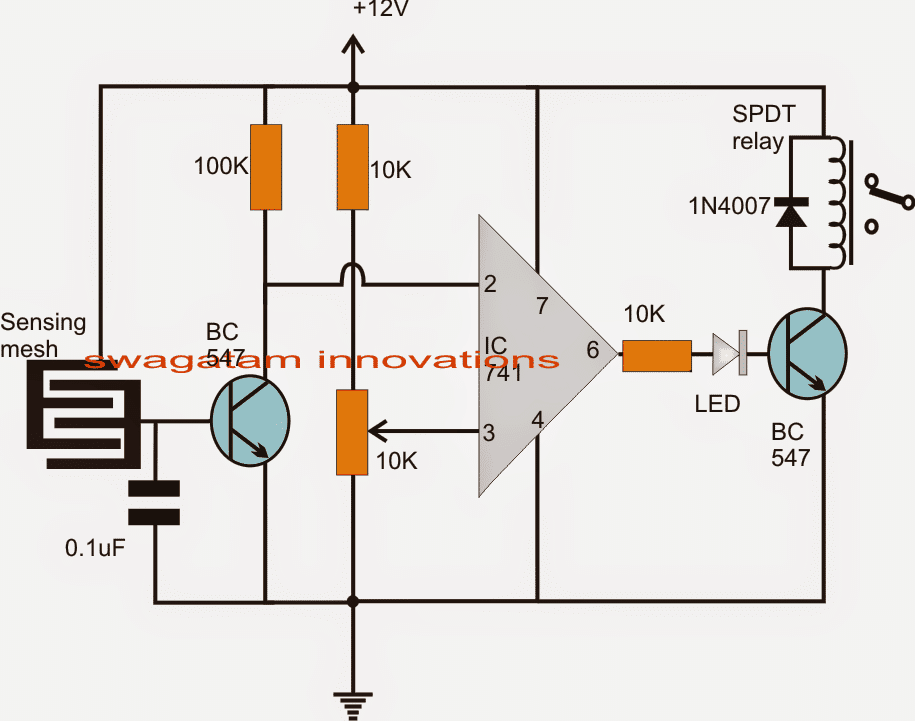
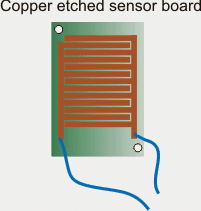
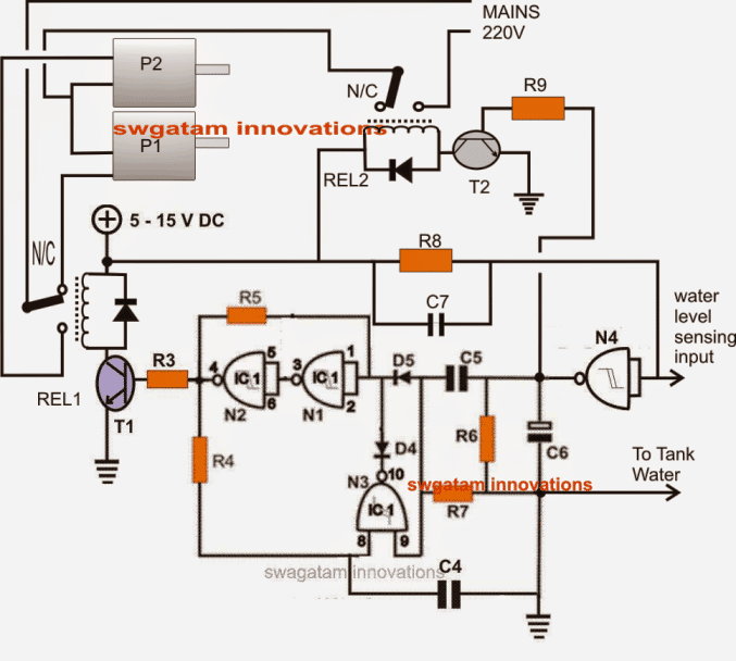
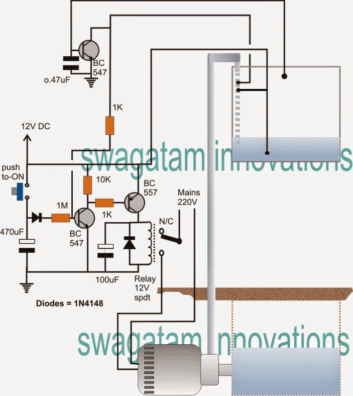
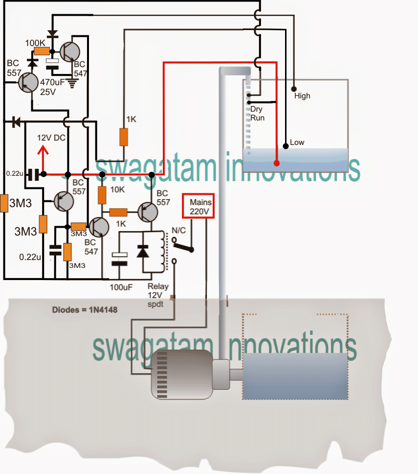
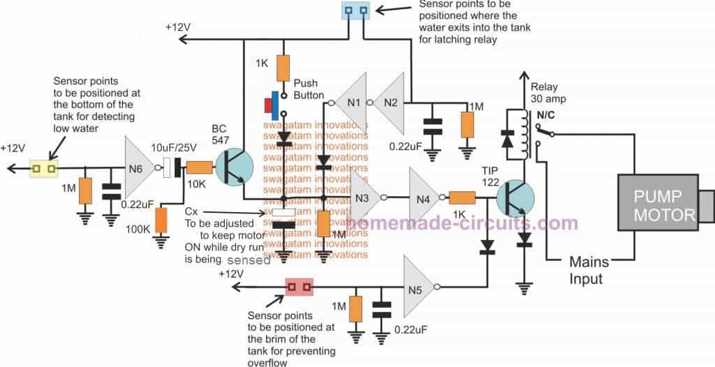 Feedback from Mr.
Prashant Zingade
Hello Swagatam,
How are you? Your Idea and logic are awesome.
hats-off to you.
I tried IC4049 version, It is working fine except one issue.(I done one modification base on your previous design and it is working now).
I am facing one issue in IC version like when we put it on auto mode, dry run function is not working.
Please see attached simulated video file.
Case 1: I observe If water level reach below bottom level relay will on pump but it fail to sense dry run and pump will continue to on.
Case 2: In manual operation it works perfectly.
Excuse for any typo.
Warm Regard
Prashant P Zingade
Feedback from Mr.
Prashant Zingade
Hello Swagatam,
How are you? Your Idea and logic are awesome.
hats-off to you.
I tried IC4049 version, It is working fine except one issue.(I done one modification base on your previous design and it is working now).
I am facing one issue in IC version like when we put it on auto mode, dry run function is not working.
Please see attached simulated video file.
Case 1: I observe If water level reach below bottom level relay will on pump but it fail to sense dry run and pump will continue to on.
Case 2: In manual operation it works perfectly.
Excuse for any typo.
Warm Regard
Prashant P Zingade
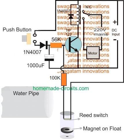
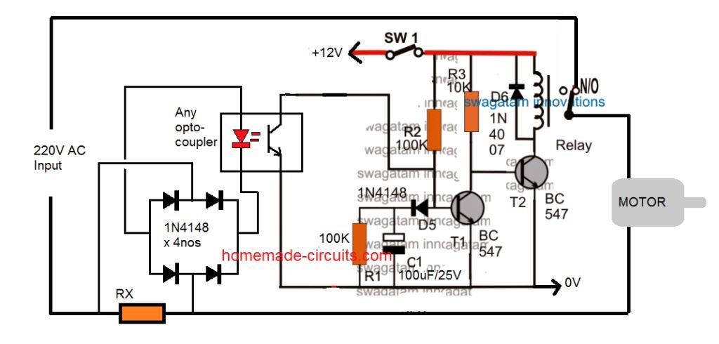 Here, the two transistors along with the associated components form a simple delay ON timer circuit.
When SW1 is switched ON, the transistor T1 remains switched OFF because of C1 which initially grounds the base drive of T1 coming via R2, while C1 charges.
This keeps T2 switched ON and the relay also switches ON.
The N/O of the relay switches ON the pump motor.
Depending on the value of C2, the motor is allowed to run for sometime.
In case there's no water, the motor runs unloaded with relatively low current passing through RX.
Due to this RX is unable to develop sufficient potential across itself, which in turn keeps the opto-coupler LED switch OFF.
This allows C1 to get charged fully unhindered during the stipulated period.
As soon as C1 is fully charged T1 switches ON, and this switches OFF T2 and also the relay.
The motor is finally shut off protecting it from a dry run situation.
On the contrary suppose the motor gets the normal supply of water, and starts pumping it normally, this instantly loads the motor causing it to consume more current.
As per the calculated value of the resistor Rx, this develops sufficient voltage across it to switch ON the LED of the opto-coupler.
Once the opto is activated C1 is inhibited from charging, and the delay ON timer is disabled.
The relay now continues to supply the 220V to the motor allowing it to run as long as water is available.
Here, the two transistors along with the associated components form a simple delay ON timer circuit.
When SW1 is switched ON, the transistor T1 remains switched OFF because of C1 which initially grounds the base drive of T1 coming via R2, while C1 charges.
This keeps T2 switched ON and the relay also switches ON.
The N/O of the relay switches ON the pump motor.
Depending on the value of C2, the motor is allowed to run for sometime.
In case there's no water, the motor runs unloaded with relatively low current passing through RX.
Due to this RX is unable to develop sufficient potential across itself, which in turn keeps the opto-coupler LED switch OFF.
This allows C1 to get charged fully unhindered during the stipulated period.
As soon as C1 is fully charged T1 switches ON, and this switches OFF T2 and also the relay.
The motor is finally shut off protecting it from a dry run situation.
On the contrary suppose the motor gets the normal supply of water, and starts pumping it normally, this instantly loads the motor causing it to consume more current.
As per the calculated value of the resistor Rx, this develops sufficient voltage across it to switch ON the LED of the opto-coupler.
Once the opto is activated C1 is inhibited from charging, and the delay ON timer is disabled.
The relay now continues to supply the 220V to the motor allowing it to run as long as water is available.
.bmp)
 The point "L" is positioned at some desired point inside the lower tank, which determines the tanks lower water level at which the motor is in the permitted zone of operation.
The terminal "O" is fixed at the topmost level of the upper tank or the overhead tank at which the motor should halt and stop filling the upper tank.
The basic switch ON sensing is done by the central NPN transistor whose base is connected to point "L", while the switch OFF action is performed by the lower NPN transistor whose base is connected to point "O".
However the above operations cannot initiate until the water itself is supplied with a positive potential or voltage.
A push-button switch has been included as requested for facilitating the required manual start function.
On pressing the given push button momentarily, allows a positive potential to enter the tank water via the push button contacts.
Assuming the lower tank level to be above the point "L" allows the above voltage to reach the base of the central transistor via the water, which instantly triggers the central transistor into conduction.
This triggering of the central transistor switches ON the relay driver stage along with the the motor, and it also latches the relay driver transistor such that now even if the push button is released sustains the operation of the circuit and the motor.
In the above latched situation, the motor halts under two conditions: either the water level goes below the point "L" or if the water is pumped until the overhead tanks upper limit is reached, that is at point"O"
With the first condition, the voltage from the relay driver collector is inhibited from reaching point "L" breaking the latch and the motor operation.
With the second condition, the lower BC547 gets triggered and breaks the latch by grounding the central transistors base.
Thus the overhead water level controller circuit is allowed to remain operational only as long as the water level is at or above point "L" or is below point "O", and also, the initialization is solely dependent on the pressing of the given push button.
The point "L" is positioned at some desired point inside the lower tank, which determines the tanks lower water level at which the motor is in the permitted zone of operation.
The terminal "O" is fixed at the topmost level of the upper tank or the overhead tank at which the motor should halt and stop filling the upper tank.
The basic switch ON sensing is done by the central NPN transistor whose base is connected to point "L", while the switch OFF action is performed by the lower NPN transistor whose base is connected to point "O".
However the above operations cannot initiate until the water itself is supplied with a positive potential or voltage.
A push-button switch has been included as requested for facilitating the required manual start function.
On pressing the given push button momentarily, allows a positive potential to enter the tank water via the push button contacts.
Assuming the lower tank level to be above the point "L" allows the above voltage to reach the base of the central transistor via the water, which instantly triggers the central transistor into conduction.
This triggering of the central transistor switches ON the relay driver stage along with the the motor, and it also latches the relay driver transistor such that now even if the push button is released sustains the operation of the circuit and the motor.
In the above latched situation, the motor halts under two conditions: either the water level goes below the point "L" or if the water is pumped until the overhead tanks upper limit is reached, that is at point"O"
With the first condition, the voltage from the relay driver collector is inhibited from reaching point "L" breaking the latch and the motor operation.
With the second condition, the lower BC547 gets triggered and breaks the latch by grounding the central transistors base.
Thus the overhead water level controller circuit is allowed to remain operational only as long as the water level is at or above point "L" or is below point "O", and also, the initialization is solely dependent on the pressing of the given push button.
 The dry run function in the above design works in the following manner:
When the water level goes below the "low level" probe, causes the positive potential to be removed from pin#2 of the IC.
This in turn causes pin#2 to go low, which instantly turns pi#3 high.
This high signal passes through the 470uF capacitor swithing ON the relay driver stage, and the pump motor is switched ON.
The relay driver and the pump remains switched ON only as long as the 470 uF charges, this may be for around 3 to 5 seconds.
Within this time span, if the pumps starts drawing water will allow the water sensor connected with the blue wires to be bridged by the pumped water.
The associated BC547 will now get the base bias and begin conducting, bypassing the 470 uF capacitor.
This will enable the relay driver BC547 to conduct freely until the full tank level is reached.
On the other hand, if suppose there's no water, and the pump runs dry, will be unable to bias the upper BC547, and eventually the 470 uF will be charged full blocking any further base current to the relay driver stage.
Due to this relay will be switched OFF preventing the dry run condition.
The dry run function in the above design works in the following manner:
When the water level goes below the "low level" probe, causes the positive potential to be removed from pin#2 of the IC.
This in turn causes pin#2 to go low, which instantly turns pi#3 high.
This high signal passes through the 470uF capacitor swithing ON the relay driver stage, and the pump motor is switched ON.
The relay driver and the pump remains switched ON only as long as the 470 uF charges, this may be for around 3 to 5 seconds.
Within this time span, if the pumps starts drawing water will allow the water sensor connected with the blue wires to be bridged by the pumped water.
The associated BC547 will now get the base bias and begin conducting, bypassing the 470 uF capacitor.
This will enable the relay driver BC547 to conduct freely until the full tank level is reached.
On the other hand, if suppose there's no water, and the pump runs dry, will be unable to bias the upper BC547, and eventually the 470 uF will be charged full blocking any further base current to the relay driver stage.
Due to this relay will be switched OFF preventing the dry run condition.
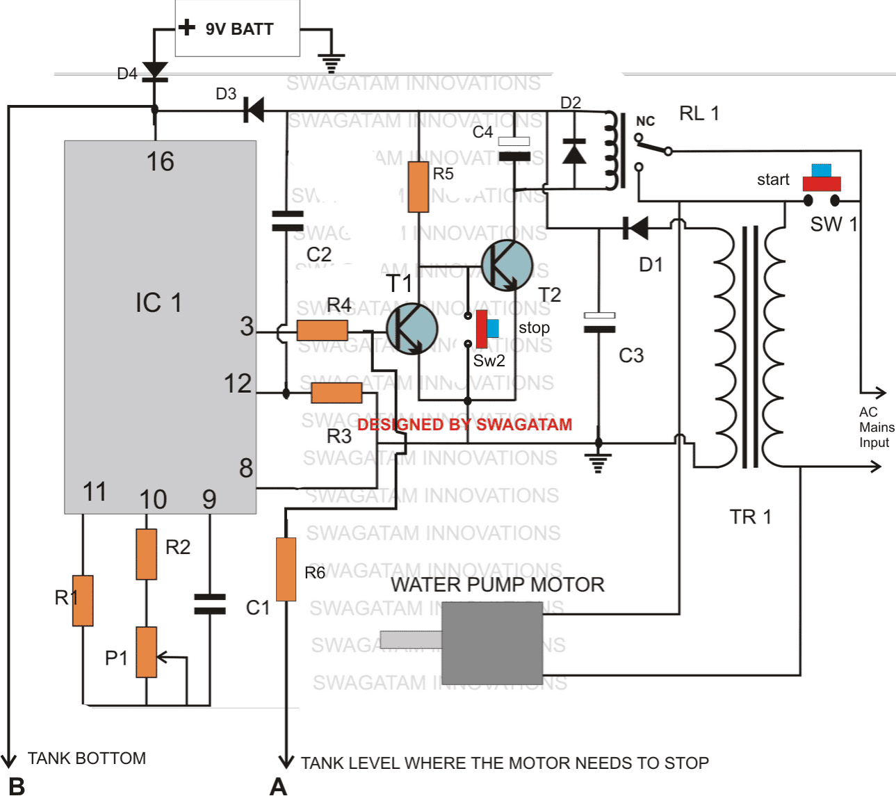
 Parts List
R1 = 15K
R2 = 330K,
R3 = 10K,
Diac resistor = 100 Ohms,
R4 = to be adjusted as explained,
C1 = 0.1uF/400V
C2, C3 = 0.1uF/250V,
L1 = 10 amp/220V choke
Triac (Alternistor) = 10 Amp 400V,
Diac = as per the above triac.
Parts List
R1 = 15K
R2 = 330K,
R3 = 10K,
Diac resistor = 100 Ohms,
R4 = to be adjusted as explained,
C1 = 0.1uF/400V
C2, C3 = 0.1uF/250V,
L1 = 10 amp/220V choke
Triac (Alternistor) = 10 Amp 400V,
Diac = as per the above triac.

 A little inspection reveals that the circuitactuallydoes not require the opto coupler circuit at all.
The circuit may be simply arranged in the following manner:
R2 should be selected such that the triac conducts only 75% of the power.
When power isswitched ON, the triac provides a softinitialstart to the motor until within the next split second when the relay also conducts enabling the motor the required full power.
This completely safeguards theactuatorcontacts from the initial current surges and sparks,
A little inspection reveals that the circuitactuallydoes not require the opto coupler circuit at all.
The circuit may be simply arranged in the following manner:
R2 should be selected such that the triac conducts only 75% of the power.
When power isswitched ON, the triac provides a softinitialstart to the motor until within the next split second when the relay also conducts enabling the motor the required full power.
This completely safeguards theactuatorcontacts from the initial current surges and sparks,
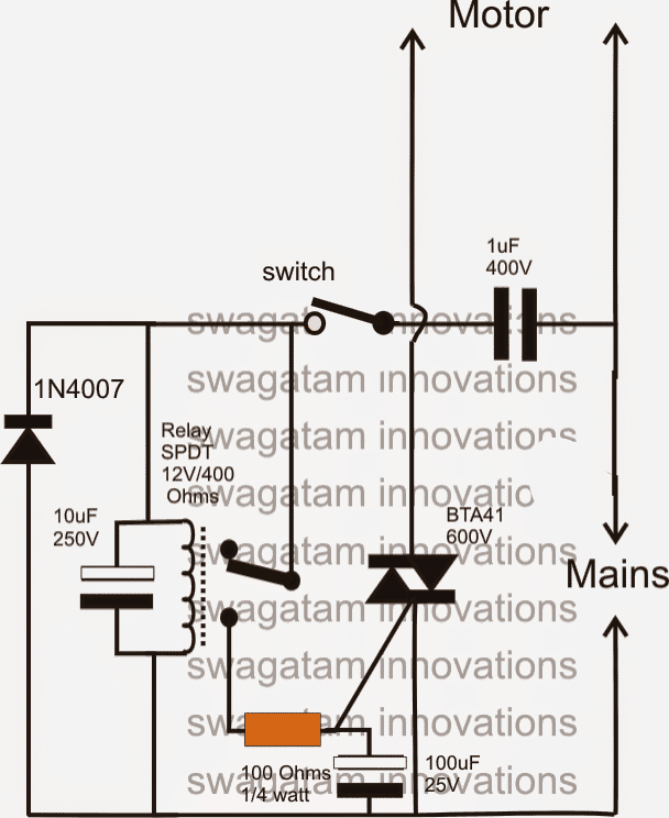 The above design can be even further simplified by removing the relay, as shown below:
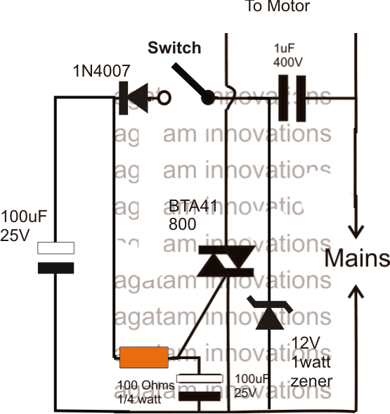 An technicallu more soundPWM based motor soft start circuit can also be tried for getting a better control, a better torque and a reliable startup for the connected motor, even for 3 phase motors.
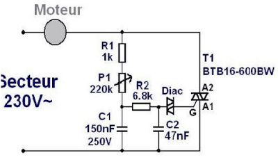 But I also use a planer/thicknesser using a motor rotating at 18000 T/min.
It seems made to notpay any royalties to evict copyrights.
Before I had problem I tought it was a motor running at 3000 t/min (2700) multiply by 2 (like others) with a belt to reach a decent speed of 6000 t/m (5400)Sorry no.
And I donˇŻt use the dimmer.
The motor run at +/- 18000 : 3 =6000 !!! Knowing the cheap cost of that machine I use it like a ˇ°good fatherˇ± not intensively etcBut one day there was a fume
The machine smoke and i dismount the machine to isolate the motor to evict the fire .
(the machine was under warranty but i need to make a lot off kilometers to make an exchange.
And there, they donˇŻt tell me it was a well known and reccurent problem ˇ but ˇ they know it! )
In fact when everything was cold .
I look the axis who rotate he seems also shooting on the opposite side of the gear belt at every start Like there wasnˇŻt a grower.
I show the motor in a company saling different kind of motor.
They make also refurbishing but they explain to me that it was an ˇ°exoticˇ± motor but they set the same diagnostic .Start to fast So come my question: Could you please make a schematic to have a ˇ°soft start / soft ending ˇ± for different universalmotors in fact if i use my dimmer system based on BTA 16 800 cw (better than the other mentioned above) it seems ok but i have only made 3 of them .
IˇŻll want to integrate that in every big machine .
And use only the on/off switch.I want use thus a button to ˇ°switch onˇ± and one to ˇ°switch offˇ± or an on/off switch.
But also a potentiometer to select the minimum level (depending the power of each motors) when the motor start running and a potentiometer to select the timing (555) between the slow start and the full speed (maybe also shortcut the triac with a relay to have full speed an a green led if it is relevant (but it will be nice) for the switch off the timing maybe reduce.
Why at the end because the extra current and problems binded.
Note : I have seen this application with ˇ°fplaˇ± or dedicated processors but I am sure it can also be done with discrete components.Why i can not do that : because I never study the motors correctly but I know for example that it is not correct to start the motor with a zero crossing system because It give a maximum current and that make the same trouble (FIRE!) with the couple at start and max current ˇ
I have seen this request in other forum touching other job mechanic wood etc ˇ with no answer and people say also if it work with a potentiometer but when you change from a machine to another you can make mistakes etcˇRegards Botte Bernard (Belgium)please donˇŻt put my adress on the net Nb i like also in your presentation the datasheet because itˇŻs no so easy to have it without paying
Bernard Botte
But I also use a planer/thicknesser using a motor rotating at 18000 T/min.
It seems made to notpay any royalties to evict copyrights.
Before I had problem I tought it was a motor running at 3000 t/min (2700) multiply by 2 (like others) with a belt to reach a decent speed of 6000 t/m (5400)Sorry no.
And I donˇŻt use the dimmer.
The motor run at +/- 18000 : 3 =6000 !!! Knowing the cheap cost of that machine I use it like a ˇ°good fatherˇ± not intensively etcBut one day there was a fume
The machine smoke and i dismount the machine to isolate the motor to evict the fire .
(the machine was under warranty but i need to make a lot off kilometers to make an exchange.
And there, they donˇŻt tell me it was a well known and reccurent problem ˇ but ˇ they know it! )
In fact when everything was cold .
I look the axis who rotate he seems also shooting on the opposite side of the gear belt at every start Like there wasnˇŻt a grower.
I show the motor in a company saling different kind of motor.
They make also refurbishing but they explain to me that it was an ˇ°exoticˇ± motor but they set the same diagnostic .Start to fast So come my question: Could you please make a schematic to have a ˇ°soft start / soft ending ˇ± for different universalmotors in fact if i use my dimmer system based on BTA 16 800 cw (better than the other mentioned above) it seems ok but i have only made 3 of them .
IˇŻll want to integrate that in every big machine .
And use only the on/off switch.I want use thus a button to ˇ°switch onˇ± and one to ˇ°switch offˇ± or an on/off switch.
But also a potentiometer to select the minimum level (depending the power of each motors) when the motor start running and a potentiometer to select the timing (555) between the slow start and the full speed (maybe also shortcut the triac with a relay to have full speed an a green led if it is relevant (but it will be nice) for the switch off the timing maybe reduce.
Why at the end because the extra current and problems binded.
Note : I have seen this application with ˇ°fplaˇ± or dedicated processors but I am sure it can also be done with discrete components.Why i can not do that : because I never study the motors correctly but I know for example that it is not correct to start the motor with a zero crossing system because It give a maximum current and that make the same trouble (FIRE!) with the couple at start and max current ˇ
I have seen this request in other forum touching other job mechanic wood etc ˇ with no answer and people say also if it work with a potentiometer but when you change from a machine to another you can make mistakes etcˇRegards Botte Bernard (Belgium)please donˇŻt put my adress on the net Nb i like also in your presentation the datasheet because itˇŻs no so easy to have it without paying
Bernard Botte
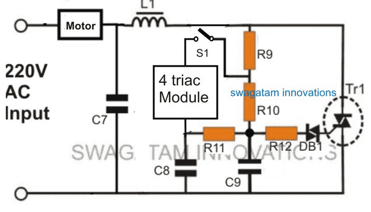
 Referring to the above diagrams, the first diagram shows a standard light dimmer or a fan dimmer switch circuit using a heavy duty triac BTA41A/600.
The section which indicates the ˇ°4 triac moduleˇ± is normally occupied with a potentiometer for enabling a manual speed control adjustment, wherein a lower resistance adjustment generates higher speed on the fan motor and vice versa.
In this soft start, soft stop design, this pot section is replaced with the indicated 4 triac module which can be elaborately visualized in the second diagram.
Here we see 4 triacs arranged in parallel having 4 individual 220K resistors at their upper MT1 arm, and 4 individual capacitors at their gates with different values, and with a sort of sequential order of high to low.
When S1 is switched ON, the triac having the lowest value capacitor switches ON first, enabling a relatively slow speed start on the motor due to switching of the relevant 220K resistor at its MT1.
Within a few millseconds the next subsequent triac conducts which has the next smaller value, and adds its own 220K resistor in parallel with the earlier 220K resistor, allowing the motor to gain some more speed.
Identically, the third and the fourth triacs also sequentially switch ON within the next few milliseconds, thereby adding two more 220K parallel resistors in the range, which finally allows the motor to reach its maximum speed.
The above sequential speed increase on the motor allows the motor to achieve the intended slow start switch ON, as desired by the user.
Quite similarly when the switch S1 is turned OFF, the relevant capacitors switch OFF in the same order but in a descending manner, which inhibits the motor from a sudden stop, instead it causes a step wise slow stop or slow end on its speed.
Feedback from Mr.
Bernard:
Dear mister Swag, First of all, thanks for your fast answer.
Because you tell me you have a timing problem I have changed my operating system to linux mint 18,1 ˇ®SerenaˇŻ so i haved to re-install all the program I need and test it (setup it!) So apparently everithings seems working OK ! About the first schematic I notice you donˇŻt give any value to the upper side schematics so I pick it up from How to Make a Simplest Triac Dimmer Switch Circuit
Parts List for the above enhanced fan dimmer circuit(C1) C7 = 0.1u/400V
(C2, C3) C8,C9 = 0.022/250V,
(R1) R9 = 15K,
(R2) R10 = 330K,
(R3) R11 = 33K,
(R4) R12 = 100 Ohms,VR1 = 220K, or 470K linear => Replaced by genial 4 triacs module
Diac = DB3,
Triac = BT136 => BTA41 600
L1 = 40uH
About the second schematic so simple solution i never have dreamed !!! to be tested asap Genial! we say in French.
I doesnˇŻt know that you can use polarized condensators for such AC applications! And also that 50 volt was sufficient! I you have a moment to explain why -
Anyway maybe iˇŻll try it this weekend if i have all the component.
I prefer use new capacitors my stock never change since 1993!
In fact i was trying different ways using for example opto triac (MOC) but i also need to pick the freq of the AC network, also another based on your schematic Kiln Temperature Controller Circuit but with up down counter 4516b and 555 etc,etc so complicated
Many thanks
Regards
B.botte
My Response:
Thanks dear Bernard,
The image which you had inserted in the conversation did not get attached properly and therefore it was not showing, but I have corrected it now and have posted it back in the article.
I have rated the caps at 50V because R9 is supposed to be a 33K or a 68K resistor which will drop the current significantly and not allow the capacitors to burn, this is my understanding.
I have used polarized capacitors because the gate of a triac works with a DC drive, but yes you are right, in order to make it DC for the capacitors we need to add a 1N4007 in series with the gate 1K resistors.
Now with regards to this design, if suppose the idea does not operate very smoothly or fails to produce the expected results, we could modify the existing gate drive for the 4 triacs into optocoupler based drivers, and perform the same sequential delayed switching but through an external DC circuit.So this circuit ultimately has the potentials to deliver the intended results, either this way or that way.Regards Swag
Referring to the above diagrams, the first diagram shows a standard light dimmer or a fan dimmer switch circuit using a heavy duty triac BTA41A/600.
The section which indicates the ˇ°4 triac moduleˇ± is normally occupied with a potentiometer for enabling a manual speed control adjustment, wherein a lower resistance adjustment generates higher speed on the fan motor and vice versa.
In this soft start, soft stop design, this pot section is replaced with the indicated 4 triac module which can be elaborately visualized in the second diagram.
Here we see 4 triacs arranged in parallel having 4 individual 220K resistors at their upper MT1 arm, and 4 individual capacitors at their gates with different values, and with a sort of sequential order of high to low.
When S1 is switched ON, the triac having the lowest value capacitor switches ON first, enabling a relatively slow speed start on the motor due to switching of the relevant 220K resistor at its MT1.
Within a few millseconds the next subsequent triac conducts which has the next smaller value, and adds its own 220K resistor in parallel with the earlier 220K resistor, allowing the motor to gain some more speed.
Identically, the third and the fourth triacs also sequentially switch ON within the next few milliseconds, thereby adding two more 220K parallel resistors in the range, which finally allows the motor to reach its maximum speed.
The above sequential speed increase on the motor allows the motor to achieve the intended slow start switch ON, as desired by the user.
Quite similarly when the switch S1 is turned OFF, the relevant capacitors switch OFF in the same order but in a descending manner, which inhibits the motor from a sudden stop, instead it causes a step wise slow stop or slow end on its speed.
Feedback from Mr.
Bernard:
Dear mister Swag, First of all, thanks for your fast answer.
Because you tell me you have a timing problem I have changed my operating system to linux mint 18,1 ˇ®SerenaˇŻ so i haved to re-install all the program I need and test it (setup it!) So apparently everithings seems working OK ! About the first schematic I notice you donˇŻt give any value to the upper side schematics so I pick it up from How to Make a Simplest Triac Dimmer Switch Circuit
Parts List for the above enhanced fan dimmer circuit(C1) C7 = 0.1u/400V
(C2, C3) C8,C9 = 0.022/250V,
(R1) R9 = 15K,
(R2) R10 = 330K,
(R3) R11 = 33K,
(R4) R12 = 100 Ohms,VR1 = 220K, or 470K linear => Replaced by genial 4 triacs module
Diac = DB3,
Triac = BT136 => BTA41 600
L1 = 40uH
About the second schematic so simple solution i never have dreamed !!! to be tested asap Genial! we say in French.
I doesnˇŻt know that you can use polarized condensators for such AC applications! And also that 50 volt was sufficient! I you have a moment to explain why -
Anyway maybe iˇŻll try it this weekend if i have all the component.
I prefer use new capacitors my stock never change since 1993!
In fact i was trying different ways using for example opto triac (MOC) but i also need to pick the freq of the AC network, also another based on your schematic Kiln Temperature Controller Circuit but with up down counter 4516b and 555 etc,etc so complicated
Many thanks
Regards
B.botte
My Response:
Thanks dear Bernard,
The image which you had inserted in the conversation did not get attached properly and therefore it was not showing, but I have corrected it now and have posted it back in the article.
I have rated the caps at 50V because R9 is supposed to be a 33K or a 68K resistor which will drop the current significantly and not allow the capacitors to burn, this is my understanding.
I have used polarized capacitors because the gate of a triac works with a DC drive, but yes you are right, in order to make it DC for the capacitors we need to add a 1N4007 in series with the gate 1K resistors.
Now with regards to this design, if suppose the idea does not operate very smoothly or fails to produce the expected results, we could modify the existing gate drive for the 4 triacs into optocoupler based drivers, and perform the same sequential delayed switching but through an external DC circuit.So this circuit ultimately has the potentials to deliver the intended results, either this way or that way.Regards Swag
 Parts procured by Ali Adnan
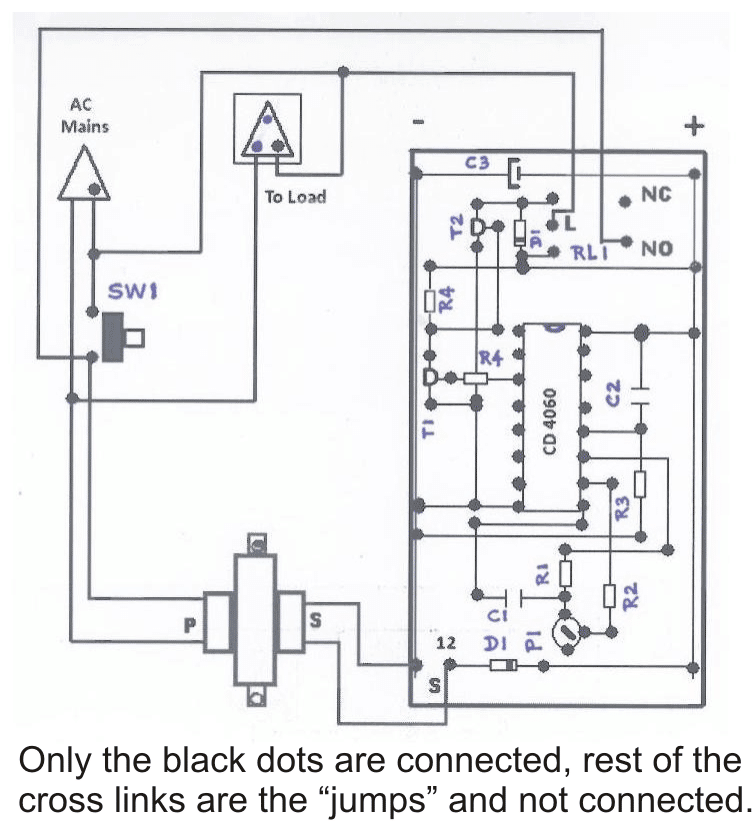 Pictures of the completed water level timer controller prototype, sent by Mr.
Raj Kumar Mukherji:
Pictures of the completed water level timer controller prototype, sent by Mr.
Raj Kumar Mukherji:
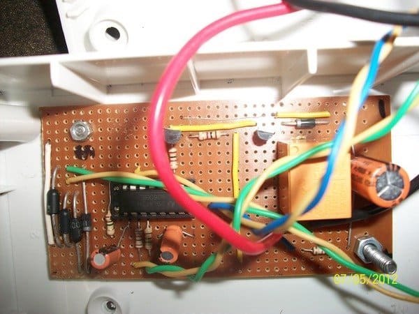 The proposed water level timer/controller circuit was further modified and enhanced Mr.Raj Mukherji, who is also an avid reader of this blog, and a keen electronic enthusiast.
Here's the feedback email that he sent to me explaining everything regarding the working of the circuit:
Finally I have managed to build, the model of this timer based water level controller project which is given below:
The proposed water level timer/controller circuit was further modified and enhanced Mr.Raj Mukherji, who is also an avid reader of this blog, and a keen electronic enthusiast.
Here's the feedback email that he sent to me explaining everything regarding the working of the circuit:
Finally I have managed to build, the model of this timer based water level controller project which is given below:
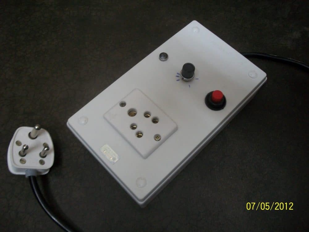 There were only three modifications I made:
1. Connected an LED to pin 7 in order to get a visual indication of the oscillation.
The LED starts to blink after 20 secs of powering the timer on
2. Used four diodes for full wave rectification instead of just a single diode for
smooth DC input
3. Added 22Mfd capacitor between pin 12 and 16 instead of 0.22Mfd because 0.22Mfd was
not allowing the oscillation to begin when the circuit was drawing power from the
transformer.
However, 0.22Mfd did not make any problem when the power was fed from
a 9 Volt battery
I have found that with the given values of the R and C, the range of this timer is between 1 - 30 mins.
I have also found the formula to calculate the frequency of the timer (it is found to work correctly to a certain extent practically):
F in KHz = 1 / {2.3 x (R2+P1) x C1} where, R2 & P1 in K Ohms, C1 in Mfd
1 Time Period (TP) in milisecs = ------------ where, F in KHz, Q(n) as shown below.
{F / Q(n)}
Pin7 = Q(4) -> divided by 16 Pin5 = Q(5) -> " " 32 Pin4 = Q(6) -> " " 64 Pin6 = Q(7) -> " " 128 Pin14 = Q(8) -> " " 256 Pin13 = Q(9) -> " " 512 Pin15 = Q(10) -> " " 1024 Pin1 = Q(12) -> " " 4096 Pin2 = Q(13) -> " " 8192 Pin3 = Q(14) -> " " 16384
Example: If P1 is set at 15 KOhms, R1 = 1 KOhm, C1 = 1 Mfd and we select the output from Pin3 (which is Q14) then:
1 1 1 F = -------------------- = ------------------ = ------------ = 0.0272 KHz {2.3 x (R2+P1) x C1} {2.3 x (1+15) x 1} 36.8
where, F = Clock frequency of the timer
Then, the frequency at Pin3 of the IC will be: 0.0272/16384 = 0.00000166 KHz
Therefore, Time Period (TP) of the timer is: 1/0.00000166 = 602409.6 miliseconds = 602.41 secs = 10.04 mins
[NOTE: Time Period = ON time + OFF time]
Hope this will help my co-readers to understand the working of the CD 4060 better.
There were only three modifications I made:
1. Connected an LED to pin 7 in order to get a visual indication of the oscillation.
The LED starts to blink after 20 secs of powering the timer on
2. Used four diodes for full wave rectification instead of just a single diode for
smooth DC input
3. Added 22Mfd capacitor between pin 12 and 16 instead of 0.22Mfd because 0.22Mfd was
not allowing the oscillation to begin when the circuit was drawing power from the
transformer.
However, 0.22Mfd did not make any problem when the power was fed from
a 9 Volt battery
I have found that with the given values of the R and C, the range of this timer is between 1 - 30 mins.
I have also found the formula to calculate the frequency of the timer (it is found to work correctly to a certain extent practically):
F in KHz = 1 / {2.3 x (R2+P1) x C1} where, R2 & P1 in K Ohms, C1 in Mfd
1 Time Period (TP) in milisecs = ------------ where, F in KHz, Q(n) as shown below.
{F / Q(n)}
Pin7 = Q(4) -> divided by 16 Pin5 = Q(5) -> " " 32 Pin4 = Q(6) -> " " 64 Pin6 = Q(7) -> " " 128 Pin14 = Q(8) -> " " 256 Pin13 = Q(9) -> " " 512 Pin15 = Q(10) -> " " 1024 Pin1 = Q(12) -> " " 4096 Pin2 = Q(13) -> " " 8192 Pin3 = Q(14) -> " " 16384
Example: If P1 is set at 15 KOhms, R1 = 1 KOhm, C1 = 1 Mfd and we select the output from Pin3 (which is Q14) then:
1 1 1 F = -------------------- = ------------------ = ------------ = 0.0272 KHz {2.3 x (R2+P1) x C1} {2.3 x (1+15) x 1} 36.8
where, F = Clock frequency of the timer
Then, the frequency at Pin3 of the IC will be: 0.0272/16384 = 0.00000166 KHz
Therefore, Time Period (TP) of the timer is: 1/0.00000166 = 602409.6 miliseconds = 602.41 secs = 10.04 mins
[NOTE: Time Period = ON time + OFF time]
Hope this will help my co-readers to understand the working of the CD 4060 better.