An Arduino three phase inverter is a circuit which produces a 3 phase AC output through a programmed Arduino based oscillator.
In this post we learn how to make a simple microprocessor Arduino based 3 phase inverter circuit which could be upgraded as per user preference for operating a given 3 phase load.
We have already studied an effective yet simple 3 phase inverter circuit in one of our earlier posts which relied on opamps for generating the 3 phase square wave signals, while the 3 phase push pull signals for driving the mosfets was implemented using specialized 3 phase driver ICs.
In the present concept also we configure the main power stage using these specialized driver ICs, but the 3 phase signal generator is created using an Arduino.
This is because creating an Arduino based 3 phase driver can be extremely complex and is not recommended.
Moreover, it is much easier to get off-the-shelf efficient digital ICs for the purpose at much cheaper rates.
Before building the complete inverter circuit, we first need to program the following Arduino code inside an Arduino UNO board, and then proceed with the rest of the details.
Arduino 3 Phase Signal Generator Code
void setup() {
// initialize digital pin 13,12&8 as an output.
pinMode(13, OUTPUT);
pinMode(12,OUTPUT);
pinMode(8,OUTPUT);
}
void loop() {
int var=0;
digitalWrite(13, HIGH);
digitalWrite(8,LOW);
digitalWrite(12,LOW);
delay(6.67);
digitalWrite(12,HIGH);
while(var==0){
delay(3.33);
digitalWrite(13,LOW);
delay(3.33);
digitalWrite(8,HIGH);
delay(3.34);
digitalWrite(12,LOW);
delay(3.33);
digitalWrite(13,HIGH);
delay(3.33);
digitalWrite(8,LOW);
delay(3.34);
digitalWrite(12,HIGH);
}
}
Original Source: http://forum.arduino.cc/index.php?topic=423907.0
The assumed waveform using the above code could be visualized in the following diagram:
Once you have burned and confirmed the above code in your Arduino, it's time to move ahead and configure the remaining circuit stages.
For this you will need the following parts which hopefully you might have already procured:
Parts Needed
IC IR2112 - 3 nos (or any similar 3 phase driver IC)
BC547 transistors - 3 nos
capacitor 10uF/25V and 1uF/25V = 3 nos each
100uF/25V = 1no
1N4148 = 3nos (1N4148 is recommended over 1N4007)
Resistors, all 1/4 watt 5%
100 ohms = 6nos
1K = 6nos
Constructional Details
To begin with, we join the 3 ICs to form the intended 3 phase mosfet driver stage, as given below:
Once the driver board is assembled, the BC547 transistors are hooked up with the HIN and LIN inputs of the IC, and illustrated in the following figure:
Once the above designs are constructed, the intended result could be quickly verified by switching ON the system.
Remember, the Arduino needs sometime to boot, therefore it is recommended to switch ON the Arduino first and then switch ON the +12V supply to the driver circuit after a few seconds.
How to Calculate the Bootstrap Capacitors
As we can see in the above figures, a circuit requires a couple of external components near the mosfets in the form of diodes and capacitors.
These parts play a crucial role in implementing precise switching of the high side mosfets, and the stages are called bootstrapping network.
Although already given in the diagram, the values of these capacitors could be specifically calculated using the following formula:
How to Calculate the Bootstrap Diodes
The above equations can be used for calculating the capacitor value for the bootstrap network, for the associated diode we have to consider the following criteria:
The diodes activate or are enabled in the forward bias mode when the high side mosfets are turned on and the potential around them is almost equal to the BUS voltage across the full bridge mosfet voltage lines, therefore the bootstrap diode must be rated enough to be able to block the full applied voltage as specified in the specific diagrams.
This looks fairly easy to understand, however for calculating the current rating, we may have to do some math by multiplying the gate charge magnitude with the switching frequency.
For example if the mosfet IRF450 is used with a switching frequency of 100kHz, the current rating for the diode would be around 12mA.
Since this value looks quite minimal and most diodes would have a much higher current rating than this normally, specific attention may not be essential.
Having said that, the over temperature leakage characteristic of the diode can be a crucial to be considered, especially in situations where the bootstrap capacitor may be supposed to store its charge for reasonably sustained amount of time.
In such circumstance the diode will need to be a ultra fast recovery type to minimize the magnitude of charge from being forced back from the bootstrap capacitor towards the supply rails of the IC.
Some Safety Tips
As we all know that mosfets in 3 phase inverter circuits can be quite vulnerable to damage due to many risky parameters involved with such concepts, especially when inductive loads are used.
I have already discussed this elaborately in one of my earlier articles, and it is strictly advised to refer to this article and implement the mosfets as per the given guidelines.
UsingIC IRS2330
The following diagrams are designed to work as a 3 phase PWM controlled inverter from an Arduino.
The first diagram is wired using six NOT gates from the IC 4049. This stage is used for bifurcating the Arduino PWM pulses into complementary high/low logic pairs so that the a bridge 3 phase inverter driver IC IC IRS2330 can be made compatible with the fed PWMs.
The second diagram from above forms the bridge driver stage for the proposed Arduino PWM, 3 phase inverter design, using the IC IRS2330 bridge driver chip.
The inputs of the IC indicated as HIN and LIN accept the dimensioned Arduino PWMs from the NOT gates and drives the output bridge network formed by 6 IGBTs which in turn drive the connected load across their three outputs.
The 1K preset is used for controlling the over current limit of the inverter by suitably adjusting it across the shut down pin of the I, the 1 ohm sensing resistor may be reduced appropriately if the current a relatively higher current is specified for the inverter.
Wrapping Up:
This concludes our discussion on how to build an Arduino based 3 phase inverter circuit.
If you have any further doubts or questions on this subject please feel free to comment and get the replies quickly.
For the PCB Gerber Files and other related files you can refer to the following link:
https://drive.google.com/file/d/1oAVsjNTPz6bOFaPOwu3OZPBIfDx1S3e6/view?usp=sharing
The above details were contributed by "cybrax"
50V 3-Phase BLDC Motor Driver
This yet another versatile 3-phase driver device in the form of IC L6235 from ST Microelectronics allows you to drive a 50V 3-phaseBLDC motor with extreme efficiency.The chip also includes all the required protection features built-in, along with an easy to configure external speed control stage.
How the IC L6235 BLDC Driver Works
The IC L6235 is an embedded DMOS 3-phase motor driver with an integrated over-current protection.
Designed with BCD technology, the device embeds the benefits of isolated DMOS power transistors with CMOS,and with bipolar circuits within the same device.
Chip Internal Structure
The chips integrates all the circuitry required for effectively driving a 3-phase BLDC motor, as explained below:
A 3-phase DMOS bridge, a constant off-time PWM current controller and the decoding logic for single ended hall sensors for generating the essential 120 degree phase shift sequence for the power stage.
With regard to the built-in protections the L6235 device offers a non-dissipative over current protection on the high-side power MOSFETs, protection against ESD, and an automatic thermal shutdown in case the device heats up above the rated value.
50V BLDC Driver Circuit Diagram
A typical L6235 50V 3-phase BLDC motor driver circuit application can be witnessed above, which looks quite straightforward with its implementation procedures.
You just have to hook up the shown elements in place and use the design to operate any BLDC motor with sensors rated within 8V to 50V at 3 amps rate.
Pinout Details
The pinout function for the specified circuit can be studied from the following data:
Pin#6, 7, 18, 19 = (GND) These are the Ground terminals of the IC.
Pin#8 = (TACHO) It's designated as the open drain output Frequency-to-voltage open drain output.
here each single pulse from pin h2is dimensioned in the form of a fixed and adjustable length pulse.
Pin#9 = (RCPULSE) Is configured like a parallel RC network attached between this pin and the ground, which fixes the period of the monostable pulse responsible for the frequency-to-voltage converter.
Pin#10 = (SENSEB) This pin must be connected together with pin SENSEA to power ground through a sensing power resistor.
Here the inverting input of the sense comparator also needs to be connected.
Pin#11 = (FWD/REV) This pinout can be used for changing the rotational direction of the BLDC motor.
A HIGH logic level on this pinout will cause a forward motion while, a LOW logic level will allow the BLDc motor to rotate in the opposite reverse direction.
For enabling a fixed clockwise or anticlockwise directions, this pinout may be appropriately terminated to a +5V or the ground line..
Pin#12 = (EN) A LOW logic signal will shut OFF all the internal power MOSFETs and stall the BLDC motor.
In case this pinout is intended to be not used, it must be terminated to the +5 V supply rail.
Pin#13 = (VREF).
You can see an opamp configured with this pinout.
The Vref input of the opamp connected with this pinout can be fed with a linearly adjustable 0 to 7V for changing the speed of the BLDC motor from 0 to max.
If not used make sure to connect this pinout to GND.
Pin#14 = (BRAKE) A LOW logic level on this pinout will switch ON all highside Power MOSFETs, instantly enforcing the brake/stop function.
In case not used, this pinout can be held connected to +5 V.
Pin#15 = (VBOOT) It is simply the input pinout for the bootstrap voltage needed for driving the upper Power MOSFETs.
Just connect the parts as indicated
Pin#5, 21, 16 = (3-phase OUT to BLDC motor) Power output which connects with the BLDC motor and powers the motor.
Pin#17 = (VSB) Just connect it as shown in the diagram.
Pin#20 = (VSA) Same as above, needs to eb connected as given in the diagram.
Pin#22 = (VCP) It is the output from the internal charge pump oscillator, connect the parts as shown in the diagram.
Pin#1, 23, 24 = 3-Phase sequential signal from the BLDC single ended Hall sensor can be configured with these pinouts, if the BLDC is a sensorless, you can feed an external 3-phase 120 degree apar input on these pinout at +5V level.
Parts List for the above discussed 50V 3-phase BLDC motor driver circuit
C1 = 100 ��F
C2 = 100 nF
C3 = 220 nF
CBOOT = 220 nF
COFF = 1 nF
CPUL = 10 nF
CREF1 = 33 nF
CREF2 = 100 nF
CEN = 5.6 nF
CP = 10 nF
D1 = 1N4148
D2 = 1N4148
R1 = 5.6 K
R2 = 1.8 K
R3 = 4.7 K
R4 = 1 M
RDD = 1 K
REN = 100 K
RP = 100
RSENSE = 0.3
ROFF = 33 K
RPUL 47 K
RH1, RH2, RH3 = 10 K
For more details you can refer to the following datasheet from ST
Compact 3-Phase IGBT Driver IC STGIPN3H60 �C Datasheet, Pinout
In this post we discuss the datasheet, and the pinout specification of the ICSTGIPN3H60 from ST microelectronics, which is perhaps the slimmest and the smartest 3-phase IGBT driver IC featuring in-built IGBTs, rated to work with 600V DC bus and upto 3 amp current, that's equivalent to almost 1800 VA handling power.
3-Phase IGBT Driver IC with Advanced Features
In this website so far we have mostly discussed and incorporated the IRS2330 (or6EDL04I06NT) for implementing a given 3 phase driver application such as a 3 phase inverter or a BLDC motor controller, and assumed this to be the easiest option using ordinary discrete components.
However with the advent of this new more compact, slim and smart 3-phase driver ICSTGIPN3H60, the earlier counterparts appear to be quite outdated, no surprise why this new IC is entitled with the name "SLLIMM" meaning small low-loss intelligent molded
module.
This is especially because the new ICSTGIPN3H60 incorporates in-built IGBTs enabling the application designs to become extremely compact and hassle free while configuring the specified parameters.
Let's not waste any more time and quickly learn the main features, and specifications of this smart 3-phase driver IC.
Main Technical Features
1) The device is a 3 phase IGBT full-bridged driver rated at 600V, 3 Amp
2) Comes with in-built full bridge 3 phase IGBT circuit, along with freewheeling protection diodes
3) Features a low electromagnetic interference working
4) Comes with an under voltage lock out, and a smart shutdown feature
5) Offers a comparator for enabling over current and over load cut off protection.
6) Includes an optional opamp in-built for enabling an advanced protection system, if demanded.
5) Possesses an in-built bootstrapping diode.
We might find a few more outstanding features in the device but we will discuss only the above main features through its pinout functions, for the sake of simplicity.
Application Areas:
The proposed IC can be used for making extremely efficient, and compact units as mentioned below:
3-phase phase inverters
3-phase BLDC motor controller
heavy lifting quadcopters
super efficient ceiling fans
E--rickshaws, and bikes
in robotics etc
Pinout description
The figure above depicts the pinout diagram of the ICSTGIPN3H60, which is a 26 pin DIL IC, we will begin the pinout functioning explanation from the left hand side of the IC.
Pin#1: It is the ground pin of the IC and needs to be connected with the ground supply rail.
Pin#2, 15: These are the SD-OD pins, any of which can be used for shutting down the device through an external sensor circuit for safeguarding the system from a possible catastrophic situation.
A "low" signal on this pinout will execute the shut-down operation.
Pin#3, 9, 13: These are the Vcc supply voltage input pinouts, for the 3 internal driver modules and must be shorted together, and connected with a common+15V DC input.
Pin#4, 10, 14: These are the HIN inputs or the high side logic signal inputs, complementary to the LIN inputs or the Low side signal inputs.
These pinouts must be fed with a 3-phase alternating 120 degrees apart logic signals from an external source or an MCU, for initiating the motor rotation.
Pin#5, 11, 16: These are the LIN inputs or the Low side logic signal inputs, complementary to the above explained HIN inputs and should be fed with alternating 3-phase low voltage triggering signals for initiating the motor rotation.
The HIN, and LIN input signals must be anti-phase to each other, meaning whenever HIN is high, the corresponding LIN must be low and vice-versa.
Pin#6, 7, 8: These are the non-inverting, output and inverting pinouts respectively of an internal spare opamp which can be suitably configured for executing a required advanced protection circuitry in case the system demands for it, otherwise these pinouts can be left unused, however make sure not to keep these opamp inputs open and floating, rather terminate these OP+, OP- pinouts through an appropriate configuration, to prevent instability across thesepinouts.
Pin#12: It is the Cin or the comparator pin of an internal comparator stage, which facilitates processing of a sensed over-current or overload signal generated by an externally configured shunt sensing resistor.
Now let's move on to the right side of the IC and see how the indicated pinouts are designated to function and how these needs to be configured within a given driver application circuit.
Pin#19, 22, 25: These are the output pinouts of the IC, and needs to be connected straight with the specified 3-phase wires of aBLDC motor, regardless of whether the motor involves sensors or not.
A motor having sensor wires can be also used with this IC.
In case the motor incorporates hall sensors, the sensor wires could be configured with the HIN/LIN pinouts, through suitable inverting gates, because the corresponding HIN/LIN inputs must be applied with anti-phase or opposite signals for correct operation of the motor, and that's why the signals from each motor hall effect sensors must be bifurcated into+/- using NOT gates for feeding the respective HIN/LIN complementary inputs of the IC.
Pin#20, 23, 26: These pinouts are the negative supply inputs for the corresponding 3-phase motor outputs, and all these pinouts must be joined together and connected with the common ground (motor bus voltage ground and IC pin#1ground)
Pin#17, 21, 24: These are the Vboot pinouts and are required to be connected with a high voltage capacitor also referred to as bootstrap capacitor.
The 3 capacitors must be configured across these pinouts and pin#19, 22, 25 or with the corresponding outputs from the IC.
In general any 1uF/1KV capacitor can be used for these caps.
Pin#18: This pinout is the bus positive supply pin, and must be attached with the motor positive supply input, which can be anything between+12V to +600V.
The above details comprehensively explain the working, the features and the pinout specification of the compact, slim 3-phase IGBT full bridge driver ICSTGIPN3H60 from ST Microelectronics.
If you have any specific question or doubt regarding the practical implementation of this device, do not hesitate to put them forth in the below given comment box.
In a few of my upcoming articles I may additionally explain how this special 3-phase IGBT full bridge driver IC could be applied for driving high power BLDC motors, inverters, and other gadgets such as high capacity drones.
3 phase Solar Submersible Pump Inverter Circuit
The post explains a simple 3 phase solar submersible pump inverter circuit which can be made by configuring a few ICs and a few power devices.
Circuit Objectives and Requirements
a three phase inverter and I connected 14 to 23 solar panels of 250 watts every solar panel 31 volts 8amp in series than I have 450 vdc to 750 vdc.
My submersible pumps 5.5kw to 7.5 kw 3phase 220v and 380v 3phase.
I also request that in the circuit auto motor speed control also needed, means when solar panel voltages up or down with the time and sunlight motor speed also adjustautomatically.
The Design
I have already explained a simple single chip 3 phase full bridge inverter circuit, the same IC can be used for the proposed solar pump inverter circuit.
The standard configuration of the 3 phase driver IC IRS2330 can be seen below:
Circuit Diagram
The above IC is outdated, but you can easily replace it with the latest IC 6EDL04
However since the mentioned 3 phase driver requires a dedicated 3 phase signal across its triggering inputs marked as HIN....LIN, it would be first important to learn about a simple 3 phase signal generator circuit using opamps which could be integrated with the above design for the intended outcome..
It doesn't need to be a sine wave 3 phase signals a simple square wave 120 degree phase shift PWM generator could be used for the application, as illustrated below:
3-Phase Generator Schematic
The above 3 phase generator circuit can be further modified in the following manner so that it can be fed to the 3 phase driver IC shown in the first image:
Using BJT Buffer Stage
Here we see how the outputs from the 3 phase generator opamps are buffered using transistor inverters for producing the required 3 out-of-phase channels for the HIN...LIN inputs of the IRS2330 3 phase inverter driver IC.
The load connected with the driver mosfets or IGBTs now would receive a square wave 3 phase operating voltage, which could be a submersible pump motor in our application as per the request.
In case the IC IRS2330 looks difficult to acquire in the local market, the following cheaper half wave solar submersible inverter circuit concept could be implemented, although with 50% less wattage efficiency.
The BJTs could be replaced with appropriately rated mosfets or IGBTs...rest of the configuration is pretty straightforward and does not need much explanation.
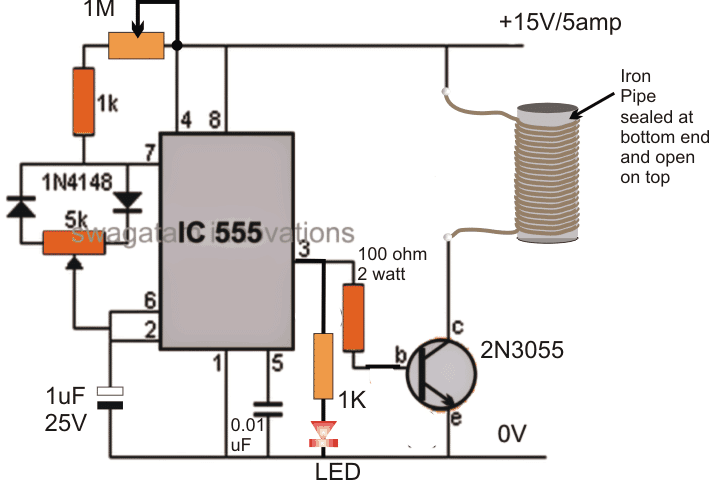
3 Phase Induction Motor Speed Controller Circuit
In this post we discuss the making of a simple 3 phase induction motor speed controller circuit, which can be also applied for a single phase induction motor or literally for any type of AC motor.
When it comes to controlling the speed of induction motors, normally matrix converters are employed, involving many complex stages such as LC filters, bi-directional arrays of switches (using IGBTs) etc.
All these are employed for ultimately achieving a chopped AC signal whose duty cycle could be adjusted using a complex microcontroller circuit, finally providing the required motor speed control.
However we can experiment and try to accomplish a 3-phase induction motor speed control through a much simpler concept using the advanced zero crossing detector opto coupler ICs, a power triac and a PWM circuit.
Using Zero Crossing Detector Opto Coupler
Thanks to the MOC series of optocouplers which has made triac control circuits extremely safe and easy to configure, and allow a hassle free PWM integration for the intended controls.
In one of my earlier posts I discussed a simple PWM soft start motor controller circuit which implemented the MOC3063 IC for providing an effective soft start on the connected motor.
Here too we use an identical method for enforcing the proposed 3 phase induction motor speed controller circuit, the following image shows how this can be done:
In the figure we can see three identical MOC opto coupler stages configured in their standard triac regulator mode, and the input side integrated with a simple IC 555 PWM circuit.
The 3 MOC circuits are configured for handling the 3 phase AC input and delivering the same to the attached induction motor.
The PWM input at the isolated LED control side of the opto determines the chopping ratio of the 3 phase AC input which is being processed by the MOC ICS.
Using IC 555 PWM Controller (Zero Voltage Switching)
That implies, by adjusting the PWM pot associated with the 555 IC one can effectively control the speed of the induction motor.
Output at its pin#3 comes with a varying duty cycle which in turn switches the output triacs accordingly, resulting in either increasing the AC RMS value or decreasing the same.
Increasing the RMS through wider PWMs enables acquiring a higher speed on the motor, while decreasing the AC RMS through narrower PWMs produces an opposite effect, that is it causes the motor to proportionately slow down.
The above features are implemented with a lot of precision and safety since the ICs are assigned with many internal sophisticated features, specifically intended for driving triacs and heavy inductive loads such as inductions motors, solenoids, valves, contactors, solid state relays etc.
The IC also ensures a perfectly isolated operation for the DC stage which allows the user to make the adjustments without the fear of an electric shock.
The principle can be also efficiently used for controlling single phase motor speed, by employing a single MOC IC instead of 3.
The design is actually based ontime proportional triac drivetheory.
The upper IC555 PWM circuit may be adjusted to produce a 50% duty cycle at much higher frequency, while the lower PWM circuit may be used for implementing the speed control operation of the induction motor through the adjustments of the associated pot.
This 555 IC is recommended to have relatively lower frequency than the upper IC 555 circuit.
This may be done by increasing the pin#6/2 capacitor to around 100nF.
NOTE: ADDING SUITABLE INDUCTORS IN SERIES WITH THE PHASE WIRES CAN DRASTICALLY IMPROVE THE SPEED CONTROL PERFORMANCE OF THE SYSTEM.
Datasheet for MOC3061
Assumed Waveform and Phase Control using the above Concept:
The above explained method of controlling a 3-phase induction motor is actually quite crude since it has no V/Hz control.
It simply employs switching the mains ON/OFF at different rates to produce an average power to the motor and control the speed by altering this average AC to the motor.
Imagine if you switch the motor ON/OFF manually 40 times or 50 times per minute.
That would result in your motor slowing down to some relative average value, yet moving continuously.
The above principle works in the same way.
A more technical approach is to design a circuit which ensures a proper control of the V/Hz ratio and automatically adjusts the same depending on the speed of the slip or any voltage fluctuations.
For this we basically employ the following stages:
H-Bridge or Full Bridge IGBT driver Circuit
3-Phase Generator Stage for Feeding the Full Bridge Circuit
V/Hz PWM Processor
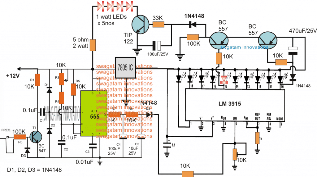
Using a Full Bridge IGBT control Circuit
If the setting up procedures of the above triac based design look daunting to you, the following full-bridge PWM based induction motor speed control could be tried:
The circuit shown in the above figure utilizes a single chip full-bridge driver IC IRS2330 (latest version is 6EDL04I06NT) which has all the features in-built in order to satisfy a safe and a perfect 3 phase motor operation.
The IC only needs a synchronized 3 phase logic input across its HIN/LIN pinouts for generating the required 3 phase oscillating output, which finally is used for operating the full bridge IGBT network and the connected 3 phase motor.
The speed control PWM injection is implemented through 3 separate half bridge NPN/PNP drivers stages, controlled with a SPWM feed from an IC 555 PWM generator as seen in our previous designs.
This PWM level may be ultimately used for controlling the speed of the induction motor.
Before we learn the actual speed control method for the induction motor, let's first understand how the automatic V/Hz control can be achieved using a few IC 555 circuits, as discussed below
The Automatic V/Hz PWM Processor Circuit (Closed Loop)
In the above sections we learned the designs which will help the induction motor to move at the rate which is specified by the manufacturer, but it won't adjust according to a constant V/Hz ratio unless the following PWM processor is integrated with the H-Bridge PWM input feed.
The above circuit is a simple PWM generator using a couple of IC 555.
The IC1 generates the PWM frequency which is converted into triangle waves at pin#6 of IC2 with the help of R4/C3.
These triangle waves are compared with the sinewave ripple at pin#5 of IC2. These sample ripples are acquired by rectifying the 3 phase AC mains into a 12V AC ripple and is fed to pin#5 of the IC2 for the required processing.
By comparing the two waveform, an appropriately dimensioned SPWM is generated at pin#3 of IC2, which becomes the driving PWM for the H-bridge network.
How the V/Hz Circuit Works
When power is switched ON the capacitor at pin#5 begins by rendering a zero voltage at pin#5 which causes the lowest SPWM value to the H-bridge circuit, which in turn enables the induction motor to start with a slow gradual soft start.
As this capacitor charges, the potential at pin#5 rises which proportionately raises the SPWM and enables the motor to gain speed gradually.
We can also see a tachometer feedback circuit which is also integrated with pin#5 of the IC2.
This tachometer monitors the rotor speed or the slip speed and generates additional voltage at pin#5 of IC2.
Now as the motor speed increases the slip speed tries to synchronize with the stator frequency and in the process it begins gaining speed.
This increase in the induction slip increases the tachometer voltage proportionately which in turn causes IC2 to increase the SPWM output and this in turn further increases the motor speed.
The above adjustment tries to maintain the V/Hz ratio to a fairly constant level until finally when the SPWM from IC2 is unable to increase any further.
At this point the slip speed and the stator speed acquire a steady-state and this is maintained until the input voltage or the slip speed (due to load) are not altered.
In case these are altered the V/Hz processor circuit again comes into action and begins adjusting the ratio for maintaining the optimal response of the induction motor speed.
The tachometer
The Tachometer circuit can be also cheaply built using the following simple circuit and integrated with the above explained circuit stages:
How to Implement the Speed Control
In the above paragraphs we understood the automatic regulation process that can eb achieved by integrating a tachometer feedback to a auto regulating SPWM controller circuit.
Now let's learn how the speed of an induction motor can be controlled by varying the frequency, which will ultimately force the SPWM to drop and maintain the correct V/Hz ratio.
The following diagram explains the speed control stage:
Here we can see a 3-phase generator circuit using IC 4035 whose phase shift frequency can be varied by varying the clock input at its pin#6.
The 3 phase signals are applied across the 4049 IC gates for producing the required HIN, LIN feeds for the full -bridge driver network.
This implies that by suitably varying the clock frequency of IC 4035, we can effectively change the operating 3-phase frequency of the induction motor.
This is implemented through a simple IC 555 astable circuit which feeds an adjustable frequency at pin#6 of IC 4035, and allows the frequency to be adjusted through the attached 100K pot.
The capacitor C needs to be calculated such that the adjustable frequency range comes within the correct specification of the connected induction motor.
When the frequency pot is varied, the effective frequency of the induction motor also changes, which correspondingly changes the speed of the motor.
For example when the frequency is reduced, causes the motor speed to reduce, which in turn causes the tachometer output to reduce the voltage proportionately.
This proportionate reduction in the tachometer output forces the SPWM to narrow down and thereby pulls down the voltage output to the motor proportionately.
This action in turn ensures that the V/Hz ratio is maintained while controlling the induction motor speed through frequency control.
Warning: The above concept is designed on theoretical assumptions only, please proceed with caution.
If you have any further doubts regarding this 3-phase induction motor speed controller design, you are most welcome to post the same through your comments.
Transistor based 3 Phase Sine Wave Generator Circuit
The post explains a very simple 3-phase sine wave generator circuit, using only three bipolar transistors and a few passive components for initiating the desired three phase output.
How it Works
Referring to the 3 phase sine wave generator circuit we can see three identical transistor stages configured in a cross coupled manner, having equivalent RC timing constants across their bases.
The 10k resistor and the 1u capacitor essentially become responsible of providing the required delay effect for generating the intended 3 phase signals with 120 degree phase shift.
When power is switched ON, the stages may seem to undergo a locked sequence, however since all the capacitors cannot have a precisely same value, the one which has a shade lower value than the other charges up first, triggering a sequential conduction across the transistor.
Let's assume that due to inconsistency in values, the middle transistor base capacitor gets charged first, this enables the middle transistor to conduct first which in turn grounds the base of the extreme right transistor preventing it from conducting for that instantaneous moment, but in the meantime the base capacitor of the left or the right transistor also gets charged in tandem which forces the middle transistor to switch OFF and release the right transistor conduction.
Push Pull Cycle
The above mutual push and pull procedure induces and settles into a continuous sequential train of conduction across the transistors causing the intended three phase signal pattern to appear across the collectors of the transistors.
Owing to the gradual charge and discharge pattern of the caapcitrs, the resultant signal shape is a pure sine wave.
The 2K2 resistor shown in yellow strangely becomes crucial in initiating the 3 phase signal generation sequence, without which the circuit seems to stall abruptly.
As mentioned before the degree of phase may be altered by changing the RC values across the bases of the transistors, here it's configured to produce a 120 degree phase shift.
Circuit Diagram
Oscilloscope trace, 3 phase waveform
Video Illustration
Since my scope was not equipped to measure 3 phase signal, I could only manage to check a single channel in the video.
Very Low Frequency Sine Wave Generator Circuit
3-Phase Motorcycle Voltage Regulator Circuits
The post discusses a list of PWM controlled simple 3 phase motorcycle voltage regulator circuit which may be used for controlling the battery charging voltage in most two wheeler.
Technical Specifications
hello my name is junior live in Brazil and work with manufacturing and recovery regulator rectifier motorcycle voltage and would appreciate a help u, I need a three-phase mosfet regulator circuit for motorcycles, entreda voltage 80-150 volts, correte Maximum 25A, maximum consumption of the system 300 watts,
I await return
att.
junior
The Design
The proposed 3 phase motorcycle voltage regulator circuit for motorcycle may be witnessed in the diagram below.
The schematic is rather easy to understand.
The 3 phase output from the alternator is sequentially applied across three power transistors which basically act like shunting devices for the alternator current.
As we all that while operating, an alternator winding could get subjected to huge reverse EMFs, to an extent which could get rip of the insulation cover of the winding destroying it permanently.
Regulating the alternator potential through the method of shunting or shorting to ground helps to keep the alternator potential under control without causing adverse effects in it.
The timing of the shunting period is crucial here and directly influences the magnitude of current that may finally reach the rectifier and the battery under charge.
A very simple way of controlling the shunting time period is by controlling the conduction of the three BJTs connected across the 3 winding of the alternator, as shown in the diagram.
Mosfets could also be used instead of the BJTs, but could be mush costlier than the BJTs.
The method is implemented by using a simple 555 IC PWM circuit.
The variable PWM output from pin3 of the IC is applied across the bases of the BJTs which in turn are forced to conduct in a controlled manner depending upon the PWM duty cycle.
The associated pot with the IC 555 circuit is appropriately adjust for obtaining the correct average RMS voltage for the battery in charge.
The method shown in the 3 phase motorcycle voltage regulator circuit using mosfets can be equally implemented for single alternators for getting identical results.
Peak voltage adjustment
A peak voltage regulation feature may be included in the above circuit as per the following diagram, in order to maintain a safe charging voltage level for the connected battery.
As can be seen, the ground line of the IC 555 is switched by the NPN BC547 whose base is controlled by the peak voltage from the alternator.
When the peak voltage exceeds 15 V, the BC547 conducts and activates the IC 555 PWM circuitry.
The MOSFET now conducts and begin shunting the excess voltage from the alternator to ground, at a rate determined by the PWM duty cycle.
The process prevents the alternator voltage exceeding above this threshold, thus ensuring that the battery is never over charged.
The transistor is BC547, and the pin5 capacitor is 10nF
Motorcycle Battery Charging System
The second design presented below is a Rectifier plus Regulator for a 3-Phase charging system of Motorcycles.
The rectifier is full-wave and the regulator is shunt-type regulator.
By: Abu Hafss
A motorcycle's charging system is different from that on cars.
The voltage alternator or generator on cars are electro-magnet type which are quite easy to regulate.
Whereas, the generators on motorcycles are permanent magnet type.
The voltage output of an alternator is directly proportional to the RPM i.e.
at high RPM the alternator will produce high voltages more than 50V hence, a regulator becomes essential to protect the entire electrical system and the battery too.
Some small bikes and 3-wheelers which do not run at high speeds, only have 6 diodes (D6-D11) to perform full-wave rectification.
They don't need regulation but those diodes are high ampere rated and dissipate a lot of heat during operation.
In bikes with proper regulated charging systems, normally shunt-type regulation is used.
This is done by shorting out the alternator's windings for one cycle of the AC waveform.
An SCR or sometimes a transistor is used as shunting device in each phase.
Circuit Diagram
Circuit Operation
The network C1, R1, R2, ZD1, D1 and D2 forms the voltage detection circuit, and it is designed to trigger at about 14.4 volts.
As soon as charging system passes this threshold voltage, T1 starts conducting.
This sends current to each gate of the three SCRs S1, S2 and S3, via current limiting resistors R3, R5 and R7. D3, D4 and D5 are important to isolate the gates from each other.
R4, R6 and R8 help in draining any possible leakage from T1. S1, S2 & S3 should be heat-sinked and isolated from each other using mica insulator, if using common heat-sink.
For the rectifier, there are three options:
a) Six automotive diodes
b) One 3-phase rectifier
c) Two bridge rectifiers
All must be rated at least 15A and heat-sinked.
The automotive diodes are two types positive body or negative body hence, should be used accordingly.
But they might be little difficult to contact to heat-sink.
Using Two Bridge Rectifiers
If using two bridge rectifiers, they may be used as shown.
Bridge Rectifier
Automotive diodes
3-phase rectifier
Bridge Rectifier
Efficient Battery Charging through Motorcycle Shunt Regulation
The following email conversation between Mr Leoneard, an avid researchers/engineer and me, helps us to learn some very interesting facts regarding motorcycle shunt regulator drawbacks and limitations.
It also helps us to know how to upgrade the concept simply into an effective yet cheap design.
Leonard:
You have an interesting circuit, but.....
My motorcycle has a 30 amp alternator, which I'm sure is RMS, and peaks at 43.2 Amps.
Your 25 Amp circuit is not likely to hold up long at all.
However.....
In place of the rectifiers you suggest, an SQL50A is rated 50 Amps at 1,000 Volts.
It is a 3-phase rectifier module, and should have no problem handling 45 amps peak.
(I have two on hand.)
That also means the SCRs will have to handle that Amperage and three HS4040NAQ2 with RMS current of 40 Amps (non-repetitive surge to 520 Amps) should handle that quite well.
Of course, they'll require a pretty healthy heatsink, and good air flow.
I'm thinking the control circuit should work pretty much as is.
I've replaced 3 regulators in the last three months and I'm about tried of throwing good money after bad.
The last one lasted a total of ten seconds before it went bad too.
I'm about to build my own and if I have to build it to power a battleship, so be it.
Another thing I've noticed, the laminations used in the alternator are considerably thicker than those used in electric motors.
An 18-pole winding, and engine operating at highway speeds means much higher frequency, and far more eddy currents in the iron.
What would be the effect on those eddy currents if using a series regulator that would allow the voltage to go as high as 70 Volts (RMS)? Would this increase the eddy currents to the point of overheating the iron, and risk damage to the windings of the alternator? If so, it would make sense not to allow the voltage to get above 14 Volts, but I still have 20 Amps coming from the alternator at 1500 RPM.
you must get rid of that high voltagewhich might put huge pressure on the alternator winding, the best way is to shunt it through heavy duty MOSFETs on heatsink
https://www.homemade-circuits.com/wp-content/uploads/2012/10/shunt-3.png
Leonard:
Actually, I'm not nearly as concerned about the effects of voltage on the windings.
They appear to be coated with Poly-Armor Vinyl, which is also used in random wound stators operating at 480 Volts.
I'm far more concerned about the heat from the eddy currents in the laminations, since they are so thick.
Here in the States, with 60 htz line current, the thickness of motor laminations are a fraction of what they are in the alternator.
At road speed, the frequency from the alternator can be 1.2 Khtz or higher.
In other applications, that would call for a ferrite core to eliminate the eddy currents.
I'm trying to understand the role of eddy currents in this application.
As RPM increases, so does the frequency, and the eddy currents as well.
A parasiticload to level off the voltage generated? A means of leveling off current generated at high RPM? Just how much heat does that generate? Enough to burn out the winding at high RPM?
Located inside the engine, I can understand using engine oil to cool the assembly, however, with the centrifugal force of the flywheel, and the windings located inside that, I can't imagine any real amount of oil getting to them for cooling.
The highest voltage I've been able to read is 70 Volts RMS.
That's not enough to arc through PAV coating on the wire, unless heat becomes excessive.
However, in shunting the excess to ground, Is there a counter EMF that opposes the magnetic field from the rotating magnets? And if so, how effective is it?
Me:
Yes, increasein frequencywill give rise to more eddy current in an iron based core, and an increase in heat.I have read that shunt control method is good for motor based generators, but this will also mean increased load on the alternator wheel and more fuel consumption by the vehicle.Is fan cooling an option? the current to the fan can be accessed from the alternator itself.
Leonard:
I'm afraid that a cooling fan is not an option for the alternator.
That is mounted internal, inside the engine, and on my Vulcan, there are two aluminum covers over that.(Replacing the alternator winding means removing the engine from the motorcycle.) I do not see any way of reducing the eddy currents because they are induced by the magnets rotating inside the flywheel.
However, I can reduce the current shunted to ground by raising the voltage of the shunt to 24 Volts, and following that with a series regulator set to 14 Volts.
In testing the alternator, I do not see much effect from counter EMF in reducing short-circuit current.
I can load the alternator to 30 Amps, and by shorting the leads, I still read 29 Amps.
However, if using the eddy currents as a parasitic load to level off the voltage and current at high RPM, it seems to be quite effective.
Once the open circuit voltage reaches 70 Volts (RMS), it does not go higher even when engine RPM doubles.
Shunting 20 Amps to ground (as done by factory regulators), increases the heat in the winding in addition to the eddy currents.
By reducing the current through the windings, the heat generated by the windings should also be reduced.
That won't reduce the eddy currents, but should reduce the overall heat generated by the alternator, hopefully preserving the winding insulation.
Considering the coating on the windings, I'm not nearly as concerned about the voltage generated.
Having worked in electric motor rebuilding for years, I'm aware that HEAT is the worst enemy of the insulation.
The quality of the insulation is reduced as operating temperature increases.
At ambient temperature, PAV coating can hold 100 Volts "turn-to-turn".
But raise that temperature by 100 C, and it may not.
I'm also curious.
Electric motors use a steel alloy with 3% silicon to reduce the resistance to magnetic field reversal within the iron.
Do they include that in their laminations or omit the silicon to further reduce the increase of voltage and current at high RPM? It does not add to the heat, but does reduce the efficiency of the iron, the higher the RPM.
By increasing the resistance to magnetic field reversal in the core, the magnetic field may not penetrate as deeply into the core before it is required to reverse.
So, the higher the RPM, the less penetration by the magnetic field.
The eddy currents may further reduce that penetration.
Me:
Your analysis makes sense and appears very much technically sound.
Being basically an electronics guy, my electrical knowledge is not very good, so suggesting motor internalworking and modifications can be difficultfor me.
But, as you said in your last sentences by restricting the magnetic filed, the eddy current can be prevented from entering deep.
I tried searching about this issue but couldn't find anythinguseful so far!
Leonard:
So, having worked with electric motors for 13 years, I have you at a slight disadvantage? Although, my studies have also been with electronics, and so was all my work until I found I could make more money working with motors.
That also meant I did not keep up with integrated circuits, and MOSFETs were delicate little things that could quickly be blown out with the slightest static charge.
So when it comes to electronics, you have me at a disadvantage.
I was not able to keep up with new developments.
It's interesting that I have not been able to find much of my information in one place.
Sort of as though none of the concepts are related to each other.
Yet, when putting them all together, they begin to make sense.
The higher the frequency, the less turns are required to get the same inductive reactance.
So the higher the RPM, the less effective the magnetic field becomes.
It's about the only way they can keep the output constant once the output reaches 70 volts.
But in looking at the pattern on an oscilloscope, I'm not impressed.
A millisecond of charge time, followed by 6 to 8 millisecond of grounded output.
Could this be why motorcycle batteries don't last long? Six months to a year, while automotive batteries go on for five years or more.
This is why I'm opting to "clip" the voltage level to ground at a higher voltage, and that clipping being constant.
Followed by a series regulator to maintain a constant charge rate according to what the battery, lights, and circuits require.
Then by designing it to handle 50 Amps, I should never have to replace a regulator again.
I'm working with a 50 Amp rating, but I expect that by using a "clipper" the Amperage should be considerably lower than 20 Amps to ground.
Perhaps as low as four Amps.
Then the series regulator allows the (approximately) seven Amps for the battery, lights, and circuits for the engine.
All well within the wattage rating of the components and not enough voltage to challenge the coating of the windings.
You wrote a very good article about shunt regulators, but 25 Amps is just too small for my application.
Still, it is good inspiration.
Me:
Yes that's right, duty cycle of 1/6 will not charge a battery properly.
But this can be easily solvedthrough a bridge rectifierand a large filter capacitor, which will ensure that the battery gets enough DC for effective charging.I am glad liked my article.
However the 25 Amp limit can be easily upgraded by increasingthe MOSFET amp specs.
Or may be by adding more devices in parallel.
Leonard:
At the same time, I'm trying to keep everything compact to fit into room available, so that large filter capacitor capacitor becomes a problem.
It is also not needed if all three phases are clipped after the bridge rectifier.
All ripple is clipped off, and the series regulator maintains 100% charge time.
Your circuit also maintains 100% charge time, however the current you shunt to ground will be much higher because you are clipping it at battery voltage.
As you can see in the waveforms, there should be no capacitor needed.
But by clipping at a higher level, the current shunted to ground should be lower.
Then, dropping the voltage across a series regulatorshould not hurt anything.
There should be more than enough to keep the battery charged.
One note.
Optimum charge voltage for a lead/acid battery is actually 13.7 volts.
To hold it at 12 volts may not give the battery enough to start the engine.
And my circuit is preliminary, and still subject to change.
The factory looks almost primitive, in the way it works.
Their circuit charges the battery until it reaches the trigger level.
then it shunts all current to ground until the battery drops below the trigger level.
The result is a waveform with a short, harsh burst of charge that could be as high as 15 Amps.
(I did not measure it) That followed by a longer line with a slight downward slope, and another burst.
I've seen automotive batteries last 5 to 10 years, or longer.
As a kid on a farm, my father converted one of the old tractors from six volts to a twelve volt system, using an alternator from a car.
Fifteen years later, that same battery was still starting the tractor.
At the school I work with (Teaches motorcycle safety), all batteries need to be replaced within one year.
WHY ? ? ? The only thing I've been able to come up with is the charging system.
Most of the batteries I've worked with are only rated for a 2 Amp charge rate, Up to 70 volts, capable of 30 Amps, applied to the battery terminals for short bursts may be causing internal damage and shortening the life of the battery.
Especially, in the batteries where you can not check the fluid levels.
The only problem with the battery may be fluid level, but there is nothing you can do about it.
If I'm able to check and maintain fluid levels, the battery life is extended considerably.
The leads coming from the alternator would be the metric equivalent of #16. According to the AWG table, that's good for 3.7 Amps as a transmission line, and 22 Amps in chassis wiring.
On a 30 Amp alternator with a shunt regulator? The shunt level and the Amperage should be an inverse proportion, so by clipping the voltage in half, I should reduce the Amperage significantly.
In looking at the rectified waveform, the highest concentration of EMF is in the lower half.
Logic would suggest the current will be reduced to a fraction.
I'll find out when I put it into use.
On a 1500cc engine, I don't expect to notice the reduced drag on the engine, but my fuel economy may improve.
And, I remember, back when they first started putting solid-state regulators on automotive alternators, the magic number was 13.7 Volts.
However, I was planning on setting my series regulator at about 14.2 Volts.
Too high and the fluid evaporates more quickly.
You were far more helpful than you know.
Originally, I had six different circuits that I was considering and was going to breadboard each of them.
Your article eliminated five of them, so I get to save considerable time and concentrate on just one.
That saves me a good amount of work.
That makes it very well worth the time to contact you.
You have my permission to experiment with my schematic and see what you come up with.
On various forums, I'm reading where a number of people are talking about going to series regulators.Others caution against too high a voltage destroying the insulated coating on the wire.
I suspect the happy medium may be a combination of both systems, but not shunting the full output to ground.
The circuit is still simple, with few components, but not archaic.
Thank you very much for your time and attention.
One of my sources for technical information is:OCW.MIT.EDU I've been doing engineering courses there for a few years now.
You don't get any credit for doing them, but it's also completely free.
How to Make a 3 Phase VFD Circuit
The presented 3 phase VFD circuit (designed by me) can be used for controlling the speed of any three phase brushed AC motor or even a brushless AC motor.
Using the VFD
The proposed 3-phase VFD circuit can be universally applied for most 3-phase AC motors where the regulation efficiency is not too critical.
It can be specifically used for controlling squirrel cage induction motor speed with an open loop mode, and possibly also in the closed loop mode which will be discussed in the later part of the article.
Modules Required for 3 Phase Inverter
For designing the proposed 3 phase VFD or variable frequency drive circuit the following fundamental circuit stages are essentially required:
PWM voltage controller circuit
3 phase high side/low side H-bridge driver circuit
3 Phase generator circuit
Voltage to frequency converter circuit for generating V/Hz parameter.
Let's learn the functioning details of the above stages with the help of the following explanation:
A simple PWM voltage controller circuit can be witnessed in the diagram given below:
The PWM Controller
I have already incorporated and explained the functioning of the above PWM generator stage which is basically designed for generating a varying PWM output across pin3 of IC2 in response to the potential applied at pin5 of the same IC.
The 1K preset shown in the diagram is the RMS control knob, which may be appropriately adjusted for acquiring the desired proportionate amount of output voltage in the form of PWMs at pin3 of IC2 for further processing.
This is set to produce a corresponding output that may be equivalent to the mains 220V or 120V AC RMS.
The H-Bridge Driver Circuit
The next diagram below shows a single chip H-bridge 3 phase driver circuit using the IC IRS2330.
The design looks straightforward as most of the complexities are handled by the chips in-built sophisticated circuitry.
A well calculated 3 phase signal is applied across the HIN1/2/3 and LIN1/2/3 inputs of the IC through a 3 phase signal generator stage.
The outputs of the IC IRS2330 can be seen integrated with 6 mosfets or IGBTs bridge network, whose drains are appropriately configured with the motor which needs to be controlled.
The low side mosfet/IGBT gates are integrated with the IC2 pin#3 of the above discussed PWM generator circuit stage for initiating the PWM injection into the bridge mosfet stage.
This regulation ultimately helps the motor to gain the desired speed as per the settings (via the 1 k preset in the first diagram).
In the following diagram we visualize the required 3 phase signal generator circuit.
Configuring the 3-Phase Generator Circuit
The 3 phase generator is constructed around a couple of CMOS chips CD4035 and CD4009 which generates accurately dimensioned 3 phase signals across the shown pinouts.
The frequency of the 3 phase signals depends on the fed input clocks which should be 6 times the intended 3 phase signal.
Meaning, if the required 3 phase frequency is 50 Hz, the input clock should be 50 x 6 = 300 Hz.
It also implies that the above clocks could be varied in order to vary the effective frequency of the driver IC which in turn would be responsible of varying the motor operational frequency.
However since the above frequency alteration needs to be automatic in response to the varying voltage, a voltage to frequency converter becomes essential.
The next stage discusses a simple accurate voltage to frequency converter circuit for the required implementation.
How to Create a Constant V/F Ratio
Typically in induction motors, in order to maintain an optimal efficiency of the motor speed and toque, the slip speed or the rotor speed needs to be controlled which in turn becomes possible by maintaining a constant V/Hz ratio.
Since the stator magnetic flux is always constant regardless of the input supply frequency, the rotor speed becomes easily controllable by maintaining the V/Hz ratio constant.
In an open loop mode, this can be done roughly by maintaining predetermined V/Hz ratios, and implementing it manually.
For example in the first diagram this may be done by suitably adjusting the R1 and the 1K preset.
R1 determines the frequency and the 1K adjusts the RMS of the output, therefore by suitably adjusting the two parameters we can enforce the required amount V/Hz manually.
However to get a relatively accurate control of an induction motor torque and speed, we have to implement a closed loop strategy, wherein the slip speed data needs to be fed to the processing circuit for an automatic adjustment of the V/Hz ratio so that this value always remains near about constant.
Implementing the Closed Loop Feedback
The first diagram on this page can be suitably modified for designing the closed loop automatic V/Hz regulation as shown below:
In the above figure, the potential at pin#5 of IC2 determines the width of the SPWM which is generated at pin#3 of the same IC.
The SPWM are generated by comparing the mains 12V ripple sample at pin#5 with triangle wave at pin#7 of IC2, and this is fed to the low side mosfets for the motor control.
Initially this SPWM is set at some adjusted level (using 1K perset) which triggers the low side IGBT gates of the 3-phase bridge for initiating the rotor movement at the specified nominal speed level.
As soon the rotor rotor begins rotating, the attached tachometer with the rotor mechanism causes an proportional additional amount of voltage to develop at pin#5 of IC2, this proportionately causes the SPWMs to get wider causing more voltage to the stator coils of the motor.
This causes further increase in the rotor speed causing more voltage at pin#5 of IC2, and this goes on until the SPWM equivalent voltage is no longer able to increase and the stator rotor synchronization attains a steady-state.
The above procedure goes on self adjusting throughout the operational periods of the motor.
How to Make and Integrate the Tachometer
A simple tachometer design can be seen in the following diagram, this could be integrated with the rotor mechanism such the rotational frequency is able to feed the base of the BC547.
Here the rotor speed data is collected from a hall effect sensor or a IR LED/Sensor network and is fed to the base of T1.
T1 oscillates at this frequency and activates the tachometer circuit made by appropriately configuring an IC 555 monostable circuit.
The output from the above tachometer varies proportionately in response to the input frequency at the base of T1.
As the frequency rises the voltage at the extreme right side D3 output also rises and vice versa, and helps to keep the V/Hz ratio to a relatively constant level.
How to Control Speed
The speed of motor using constant V/F can be achieved by altering the frequency input at the clock input of IC 4035. This can be achieved by feeding a variable frequency from a IC 555 astable circuit or any standard astable circuit to the clock input of IC 4035.
Changing the frequency effectively changes the operating frequency of the motor which correspondingly lowers the slip speed.
This is detected by the tachometer, and the tachometer proportionately reduces the potential at pin#5 of the IC2 which in turn proportionately reduces the SPWM content on the motor, and consequently the voltage for the motor is reduced, ensuring motor speed variation with the correct required V/F ratio.
A Homemade V to F Converter
In the above voltage to frequency converter circuit a IC 4060 is used and its frequency dependent resistance is influenced through a LED/LDR assembly for the intended conversions.
The LED/LDR assembly is sealed inside a light proof box, and the LDR is positioned across a 1M frequency dependent resistor of the IC.
Since the LDR/LDR response is fairly linear, the varying illumination of the LED on the LDR generates a proportionately varying (increasing or decreasing) frequency across pin3 of the IC.
The FSD or the V/Hz range of the stage could be set by appropriately setting up the 1M resistor or even the C1 value.
The LED is voltage is derived and illuminated through the PWMs from the first PWM circuit stage.
It implies that as the PWMs vary, the LED illumination will also vary which in turn would give rise to a proportionately increasing or decreasing frequency at pin3 of the IC 4060 in the above diagram.
Integrating the Converter with VFD
This varying frequency from the IC 4060 now simply needs to be integrated with the 3 phase generator IC CD4035 clock input.
The above stages form the main ingredients for making a 3 phase VFD circuit.
Now, it would be important to discuss regarding the DC BUS required for supplying the IGBT motor controllers and the setting up procedures for the entire design.
The DC BUS applied across the IGBT H-bridge rails may be obtained by rectifying the available 3 phase mains input using the following circuit configuration.
The IGBT DC BUS rails are connected across the points indicated as "load"
For a single phase source the rectification may be implemented using standard 4 diode bridge network configuration.
How to Set Up the proposed 3 phase VFD circuit
It may be done as per the following instructions:
After applying the DC bus voltage across the IGBTs (without the motor connected) adjust the PWM 1k preset until the voltage across the rails become equal to the intended motor voltage specs.
Next adjust the IC 4060 1M preset in order to adjust any of IC IRS2330 inputs to the required correct frequency level as per the given motor specifications.
After the above procedures are completed, the specified motor may be connected and supplied with different voltage levels, V/Hz parameter and confirmed for an automatic V/Hz operations over the connected motor.
3 Phase Brushless (BLDC) Motor Driver Circuit
In this post we learn how to make a simple 3 phase brushless DC motor driver circuit.
The circuit employs the popular IRS2330 3-phase driver IC
The presented idea looks simple since most of the technicalities is taken care of efficiently by the IC itself, it's all about connecting the relevant pinouts with the few external supplementary components for the required implementations.
How BLDC with Hall Sensors Work
We know that all BLDC motors fundamentally incorporate Hall sensors attached with their stator assembly where these devices play a crucial rule in detecting and supplying the control circuit with the necessary data regarding the rotor magnet instantaneous positions with regard to the stator coil activation.
The info helps the control circuit to subsequently changeover the stator electromagnet activations sequentially such that the rotor constantly experiences a rotational torque and produces the intended rotational motion.
Therefore it seems that the hall effect sensors are the ones that become solely responsible for detecting and inducing the intended rotational motion in BLDC motors.
The control circuit connected with the hall sensors are in fact "blind" and respond entirely to the hall sensor signals in order to produce the required feed backs to the electromagnet coils.
The above fact actually makes the designing of a 3 phase BLDC motor controller pretty easy, the simplicity also becomes further aided with the easy availability of the universal 3 phase H bridge driver IC such as the IRS2330.
Studying the IC IRS2330 Specifications
The following discussion provides a comprehensive view on the designing of a 3 phase brushless BLDC motor driver circuit:
Pinout Details of the IC
The above shows the pinout diagram of the IC IRS2330 which simply needs to be connected to a set of a few external components for implementing the proposed BLDC controller circuit.
How to Configure the Full Bridge IC
In the above diagram we witness the method of connecting the IC pinouts with some external components wherein the right hand side IGBT stage shows a standard H bridge configuration using 6 IGBTs integrated with the appropriate pinouts of the IC.
The above integration concludes the output power stage for the BLDC controller circuit, the "load" indicates the BLDC 3 phase electromagnet coils, now its all about configuring the inputs HIN1/2/3 and LIN1/2/3 of the IC with the relevant hall sensor outputs.
NOT gates for Sequencing the HIN, LIN Inputs
Before applying the hall sensor triggers to the driver IC inputs, it's required to be buffered through a couple of NOT gates as given in the diagram above.
Finally, the outputs of the NOT gates is integrated appropriately with the inputs of the IC IRS2330.
The negatives of all the hall sensors may be assumed to be grounded.
The second circuit which forms the main driver configuration for the proposed 3 phase brushless BLDC motor driver circuit, could be also seen having a current sensing stage across its lower left section.
The resistive divider may be appropriately dimensioned for enabling an over current protection and control over the connected BLDC motor.
For getting comprehensive details regarding the current sensing configuration and other intricacies of the whole design, one may refer to the following datasheet of the IC:
https://www.irf.com/product-info/datasheets/data/irs2330pbf.pdf
How to Convert 3 phase AC to Single phase AC
The post discusses how to convert 3 phase AC to single phase AC through a special bridge rectifier at any desired voltage.
Technical Specifications
You have a very nice page and I find it really good, If been looking for a 380V 3ph converter to 230V, it should with held at least 3-5 KVA.
Not sure if you have one or
would you be able to direct me to one.
I have a 3ph input of 5.5KVA from a generator that I would like to convert to one single output of 230V +- 3-5 KVA.
Doing the usual ph to neutral per ph would not give me a strong KW output.
Transformers are very expensive.
I would appreciate your help thank you.
Chaquito
The Design
The question how to convert 3 phase AC to single phase AC can be solved by first rectifying the 3 phase AC to DC and then converting the DC back to 220 V AC through a full bridge driver IC and H-bridge mosfet network.
The first stage intended for converting the 3 phase AC to DC may be executed simply by the traditional diode bridge network, as may be witnessed in the following diagram.
After filtration this would produce a peak of 530 V (with a filter capacitor of around 10uF/1kv included across the load)
Now, once the 3 phase rectified DC is achieved, this will need to be converted to the desired single phase AC, as per the request this value should be 220 V.
A full bridge mosfet driver topology may be incorporated for implementing the above requirement, as shown in the following diagram:
The layout looks simple and easy to configure, however it would produce and subject the load to the full 530 V instead of the specified 220 V.
The issue can be normalized and controlled to the desired levels through an external voltage sensor circuit, which could be further integrated with the Ct pin of the IC IRS2453.
The simple solution can be implemented by incorporating the following circuit:
The 220k preset is adjusted precisely so that the transistor just begins conducting at voltages around 240 V across the load.
When the transistor conducts, the Ct pin is grounded at that instant, forcing the IC to inhibit its oscillations which in turn renders the high side outputs to go low, cutting off the rectified high voltage to the mosfets.
This results in lowering down of the voltage across the load which allows the BC547 to switch OFF and restore the IC operations....the procedure repeats making sure that the output stays under control and at the specified 220 V level.
Single Phase Voltage from Three Phase Voltage Source
The post explains a simple relay changeover circuit for extracting single phase AC from a three phase AC source irrespective of the condition whether all the three phases are present or not.
Technical Specifications
hi sir please i need somethingI'vebeen searching everywhere but not avail so please I'm appealing to you if youcan do it for me, this is special request,
The thing is in my country we have 3 phase meter and single phase meter so if you use single phase meter you are able to get one phase AC power and negative from the electricity-pole,
But sometime one phase go off and also low voltage problems exist, so sir what i am requesting you is to design for me a 3 phase changeover which will bring all the 3 power from the electricity pole for the attached single phase meter so that when any one phase power goes off or low current then it changes to another phase.
I have tried one such circuit for changing the second alternate phase when one phase goes off, however when it comes back again while the other one is not off which becomes very dangerous.
so i will be glad if you can design me one 3 phase changeover circuit.
thank you sir looking forward to hear from you.
The Design
The circuit of the proposed changeover circuit which can be used for getting a single phase AC from a three phase AC source even with missing phases is shown the following diagram.
Although the circuit looks technically correct and safe, it won't respond to low voltage or brownout conditions, so perhaps additional stages would be required for facilitating this feature.
As can be seen the circuit would be able to supply a single phase power to the load no matter whether all the phases are present or if a couple of them are missing and also irrespective of the phase serial number.
Suppose all the three phases are present, this would allow the left transistor relay to stay activated while keeping the other two stages switched OFF.
With only phase1 present, the same would be applied as above.
With phase2 and phase3 present and phase1 off, the center transistor stage would operate while the remaining would remain switched OFF.
With only the third phase present and the other two missing would activate the right most relay stage while keeping the other two switched off.
Therefore under all situations the load would be allowed to access the single phase power from the given 3 phase source.
The ground indicated connection must be terminated to the pole as suggested by Mr.Biannz.
Circuit Diagram
Parts list
All resistors are 10k, 1/4 watt
All non-polar capacitors = 105/400V
All polar capacitors are = 100uF/25V
All zener diodes are = 12V/ 1watt
All transistors are = BC547
All relays are = 12V/spsdt, 12amp/400mA
All rectifier diodes are = 1N4007
WARNING: THE ABOVE CIRCUIT IS NOT ISOLATED FROM MAINS AC AND ALL THE CIRCUIT POINTS COULD BE AT LETHAL MAINS POTENTIAL, EXERCISE EXTREME CAUTION WHILE MAKING IT, AND DO IT AT YOUR OWN RISK.
Upgrading the above Circuit
The following single phase voltage from three phase voltage source circuit shows how the above earlier circuit can be upgraded using a bridge network circuit for better response.
Simple 3 Phase Inverter Circuit
The post discuses the how to make a 3 phase inverter circuit which can be used in conjunction with any ordinary single phase square wave inverter circuit.
Arduino 3 phase inverter
The Circuit Concept
A 3 phase load can be operated from a single phase inverter by employing the following explained circuit stages.
Basically the involved stages can be divided into three groups:
The PWM generator circuit
The 3 phase signal generator circuit
The mosfet driver circuit
The first diagram below shows the PWM generator stage, it may be understood with the following points:
The Oscillator and the PWM Stage
The IC 4047 is wired as a standard flip flop output generator at the rate of the desired mains frequency set by VR1 and C1.
The dimensioned push-pull PWM now becomes available at the E/C junction of the two BC547 transistors.
ThisPWM is applied to the input of the 3 phase generator explained in the next section.
The followingcircuitshows a simple three phase generator circuit which converters the above input push-pull signal into 3 discrete outputs, phase shifted by 120 degrees.
These outputs are further bifurcated by individual push-pull stages made from a NOT gates stages.
These 3 discrete 120 degree phase shifted, push pull PWMs now become the feeding input signals (HIN, LIN) for the final 3 phase driver stage explained below.
This signal generator uses a single 12V supply and not a dual supply.
Complete explanation can be found in this 3 phase signal generator articleThe circuit below shows a 3 phase inverter inverter circuit stage using H-bridge mosfets configuration which receives the phase shifted PWMs from the above stage and converts them into corresponding high voltage AC outputs for operating the connected 3 phase load, normally this would be a 3 phase motor.
The 330 high voltage across the indivdual mosfet drivers sections is obtained from any standard single phase inverter integrated across the shownmosfets drains for powering the desired 3 phase load.
The 3-Phase Full-Bridge Driver Stage
In the above 3 phase generator circuit (second last diagram) using a sine wave doesn't make sense because the 4049 would ultimately convert it into square waves, and moreover the driver ICs in the last design employ digital ICs which will not respond to sine waves.
Therefore a better idea is to use a 3 phase square wave signal generator for feeding the last driver stage.
You may refer the article which explains how to make a 3 phase solar inverter circuit for understanding the 3 phase signal generator stage functioning and implementation details.
Using IC IR2103
A relatively simpler version of the above 3 phase inverter circuit can be studied below, using the IC IR2103 half bridge driver ICS.
This version lacks the shut down feature, therefore if you do not wish to incorporate the shut down feature, you can try the following simpler design.
Simplifying the Above Designs
In the above explained 3-phase inverter circuit, the 3-phase generator stage looks unnecessarily complex, and therefore I decided to look for an alternative easier option for replacing this specific section.
After some searching I found the following interesting 3 phase generator circuit which looks pretty easy and and straightforward with its settings.
Therefore now you can simply replace the earlier explained IC 4047 and the opamp section entirely and integrate this design with HIN, LIN inputs f the 3 phase driver circuit.
But remember you will have to still use the N1----N6 gates between this new circuit and the full bridge driver circuit.
Making a Solar 3 Phase Inverter Circuit
So far we have learned how to make a basic 3 phase inverter circuit, now we'll see how a solar inverter with a 3 phase output can be built using very ordinary ICs and passive components.
The concept is basically the same, I have just changed the 3 phase generator stage for the application.
Inverter Basic Requirement
For acquiring a 3 phase AC output from any single phase or a DC source we would require three fundamental circuit stages:
A 3 phase generator or processor circuit
A 3 phase driver power stage circuit.
A boost converter circuit
Solar Panel (appropriately Rated)
To learn how to match a solar panel with battery and inverter, you can read the following tutorial:
Calculate solar Panels for Inverters
One good example may be studied in this article which explains a simple 3 phase inverter circuit
In the present design we too incorporate these three basic stages, let's first learn regarding the 3 phase generator processor circuit from the following discussion:
How it Works
The diagram above shows the basic processor circuit which looks complex but actually it's not.
The circuit is made up of three sections, the IC 555 which determines the 3 phase frequency (50 Hz or 60 Hz), the IC 4035 which splits the frequency into the required 3 phases separated by a phase angle of 120 degrees.
R1, R2 and C must be appropriately selected for acquiring a 50 Hz or 60 Hz frequency at 50% duty cycle.
8 numbers NOT gates from N3 to N8 can be seen incorporated simply for splitting the generated three phases into pairs of high and low logic outputs.
These NOT gates may be acquired from two 4049 ICs.
These pairs of high and low outputs across the shown NOT gates become essential for feeding our next 3 phase driver power stage.
The following explanation details the solar 3 phase power mosfet driver circuit
Note: The shut down pin must be connectedto the ground line if not used, otherwise the circuit will not work
As may be seen in the above figure, this section is built across 3 separate half bridge driver ICs using IRS2608 which are specialized for driving high side and low side mosfet pairs.
The configuration looks quite straightforward, thanks to this highly sophisticated driver IC from International rectifier.
Each IC stage has its own HIN (high In) and LIN (low In) input pins and also their respective supply Vcc/ground pins.
All the Vcc are required to be joined together and connected with the 12V supply line of the first circuit (pin4/8 of IC555), so that all the circuit stages become accessible to the 12V supply derived from the solar panel.
Similarly all the ground pins and lines must be made into a common rail.
The HIN and LIN should be joined with the outputs generated from the NOT gates as specified in the second diagram.
The above arrangement takes care of the 3 phase processing and amplification, however since the 3 phase output should be at the mains level and a solar panel could be rated at a maximum of 60V, we must have an arrangement that would enable boosting this low 60 volts solar panel to the required 220V or 120V level.
Using IC 555 Based Flyback Buck/Boost Converter
This can be easily implemented through a simple 555 IC based boost converter circuit as may be studied below:
Again, the shown configuration of the 60V to 220V boost converter looks not so difficult, and can be constructed using very ordinary components.
The IC 555 is configured as an astable with a frequency of approximately 20 to 50 kHz.
This frequency is fed to the gate of a switching mosfet via a push pull BJT stage.
The heart of the boost circuit is formed with the help of a compact ferrite core transformer which receives the driving frequency from the mosfet and converter the 60V input into the required 220V output.
This 220V DC is finally attached with the previously explained mosfet driver stage across the drains of the 3 phase mosfets for achieving the 220V 3 phase output.
The boost converter transformer can be built on any suitable EE core/bobbin assembly using 1mm 50 turns primary (two 0.5mm bifilar magnet wire in parallel), and secondary using o.5 mm magnet wire with 200 turns
Driving 3-Phase Motor on Single Phase Supply
Driving a three phase motor on a single phase supply directly through ordinary methods can be difficult and dangerous.
It requires accurately designed circuits for implementing the operations.
Here I have tried to present one such PWM controlled three phase motor driver circuit.
Let's learn more.
The circuit can be understood with the following points:
Circuit Operation
Before going to the following explaination it would be important to know regarding a three phase signal generator circuit explained here: https://www.homemade-circuits.com/2013/09/three-phase-signal-generator-circuit.html
The above circuit becomes the crucial part of the whole design because it's this stage which provides the 120 degree phase shifted signals for driving the proposed 3 phase motor driver stages from a single phase source.
All the involved circuits are operated from a common 12V DC source which may be obtained from a standard AC/DC adapter configuration using a 12V transformer, bridge and capacitor network.
In the first diagram shown below we see a simple 555 PWM generator circuit which generates equivalent modified sine wave PWM waves at its pin#3.
These are generated in response to sine waves from the outputs of the 3-phase signal generator circuit as explained in the above given link.
That means we would require three such identical 555PWM generator stages for processing the three outputs from the 3-phase signal generator opamps.
The outputs from the respective three PWM generators as referred HIN and LIN are fed to the inputs of three discrete mosfet driver circuits, shown in the second diagram below.
We use the IC IR2110 for the driver part of the circuits, three separate IC drivers are used for processing the three PWM outputs from the 555 sections.
The outputs from the mosfets are directly connected with the three wires of the motor.
The 330V to the mosfetsis derived by rectifying the mains single phase AC.
Circuit Diagram
3-Phase Signal Generator Circuit using Opamp
Many a times we find it crucial and handy to possess a true three phase signal for evaluating many different electronic configurations such three phase inverters, three phase motors, converters etc.
Since it's not so easy to incorporate single phase to three phase conversion quickly we find this particular implementation difficult to acquire and enforce.
The proposed circuit enables the above discussed well calculated spaced and positioned sine waves outputs to be generated from a single master input source.
Circuit Operation
The circuit functioning of the three phase waveform generator circuit may be understood with the help of the following explanation:
An input sine sample waveform is fed across the point "input" and ground of the circuit.This input signal gets inverted and buffered by the unity gain opamp A1. This inverted and buffered signal acquired at the output of A1 now becomes the new master signal for the forthcoming processing.
The above buffered master signal gets once again inverted and buffered by the next unity gain opamp A2 creating an output with zero degree initial phase across the points "Phase1"
Simultaneously, the master signal from A1 output is phase shifted by 60 degrees via the RC network R1, C1, and fed to the input of A4.
A4 is set up as a non-inverting opamp with a gain of 2 in order to make up for the signal-loss in the RC configuration.
On account of the fact that the master signal is phase shifted 180 degrees from the input signal, and further shifted to an additional 60 degrees by the RC network, the ultimate output waveform gets shifted by 240 degrees, and constitutes the "Phase3" signal.
Now, the next unity gain amp A3 sums up the A1 output (0 degrees) with A4 output (240 degrees), creating a 300 degree phase shifted signal at its pin#9, which is in turn inverted appropriately, shifting the phase to an extra 180 degrees, creating the intended 120 degree phase signal across its output indicated as "Phase2".
The circuit is intentionally wired up to work with a fixed frequency in order to yield better accuracy.
Fixed values are used for R1 and C1 for rendering the intended, accurate 60 degree phase shifts.
For specific customized frequencies, you may use the following formula:
R1 = (��3 x 10^6) / (2�� x F x C)
R1 = (1.732 x 10^6) / (6.28 x F x C1)
where:
R1 is in kohms
C1 is in uf
Circuit Diagram
Parts List
All R = 10 kohms
A1---A4 = LM324
Supply = +/- 12vdc
Frequency (hz)
R1(kohms)
C1(nf)
1000
2.7
100
400
6.8
100
60
4.7
1000
50
5.6
1000
The above design was investigated by Mr.
Abu-Hafss and appropriately corrected for obtaining legitimate responses from the circuit, the following images provide a detailed info regarding the same:
Feedback from Mr.
Abu-Hafss:
I needed a 15VAC 3-phase supply to test 3-phase rectifiers.
I simulated this circuit the other day but failed to get proper results.
Today, I made it work.
IC A2 and resistors connected to pin 6 could be eliminated.
The resistor between pin 7 and 9 could be connected between the main input and pin 9. Phase-1 output can be collected from the original AC input.
Phase 2 and 3 can be collected as indicated in the circuit.
However, my actual requirement could not be fulfilled.
When these 3 phases are connected to a 3-phase rectifier, the wave form of phase 2 and 3 gets disturbed.
I tried with the original circuit, in that case all three phases gets disturbed
Finally got a solution! A 100nF capacitor connected in series with each phase and the rectifier solved the problem to a great extent.
Though the rectified output is not consistent but, it is quite acceptable
Update:The following image shows a much simpler alternative for generating 3 phase signals with accuracy and without complicated adjustments:
Single Phase AC to Three Phase AC Converter Circuit
The post explains an interesting single phase AC to 3 phase AC circuit.
The idea was requested by Mr.
Sachin Sinalkar.
Technical Specifications
Hi dear sir,
is there any way by which we can convert single phase 230V supply into three phase.
i had try to ask question on your web site but couldn't succeed.
i know that you can do it.i got one diagram from internet the name written on diagram that 230v ac to 400v dc power supply.
i had try according to ckt diagram but it make 700v ac supply only at one time but after next it won't worked.
at next time my electricity board burn.
Actually it is not for any purpose just one thought came in my mind and i think if it possible it will be really helpful for all of us since in village there is so much of load shading problem.
But one think good in few villages that at night for homes single phase supply available of farmer's crop wasted since they couldn't supply water to there crop if this happen it will be miracle.
The Design
I am not very sure regarding the working feasibility of the presented design, I hope it would function as expected from it.
The circuit is basically a voltage amplifier which is able to amplify a source input voltage to the level that's applied across the mosfets.
Three identical circuits need to be built for implementing the proposed single phase to three phase converter circuit design idea.
Making an accurate three phase input source wasdifficult to design and implement therefore I thought of a rather unusual method of generating the required three phase input pattern.
Since normally the load at the output of the proposed design would be a three phase motor so initially this motor could be rotated manually such that it behaves like a three phase alternator generating the required initial sample three phase voltage for the amplifier input.
As shown in the circuit diagram, we need three such identical circuits connected with the three wires of the motor integrated with their outputs.
We can see that a feedback link from the mosfet output been applied to the input of the amplifier.
With the given conditions if the connected three phase motor is rotated at the specified frequency, a sample equivalent voltage/frequency would be fed back at the input.
This input would then get amplified and returned at the required high potential AC voltage to the motor, locking its rotation in that particular frequency, once this takes place the manual rotation could be stopped and hopefully the latching would sustain the influence as long as the 330V DC continues to exist across the mosfets.
The manual rotation of the connected three phase motor could be done through an external single phase motor coupled with the three phase motor using gears which could be detached by some suitable mechanism as soon the system gets latched.
Of course this is just an idea from my part, if there's any feasibility in this idea it can enhanced or improved through suitable modifications.
The left hand side driver section requires 12V DC which can be acquired via a standard AC/DC adapter while the mosfet supply can be obtained from a bridge rectifier network directly connected with the existing 220 or 120V single phase source.
Circuit Diagram
Devices required for the above single phase to three phase converter circuit.
Q1, Q2 = BC557,
Q3 = BD140
Q4, Q5 = BD139
Mosfets = 600V 1 amp, or approximate equivalent
Prevent Amplifier Fuse from Blowing During Power Switch ON
Is your power amplifier fuse blowing during power switch ON? It could be happening due to the initial high current drawn by the loudspeakers, when power is switched ON.
The simple amplifier fuse protection circuits presented here can be effectively used for solving the issue.
The problem is commonly seen in high power amplifiers, where the loudspeakers have low resistance specs, or in power amplifiers which have many high power loudspeakers connected in parallel.
Why Amplifier Fuses Blow
In high power amplifiers, when power is switched ON, the various stages inside the circuit board take a few milliseconds to stabilize.
However, before the circuit stages are able to stabilize, the MOSFETs are forced to conduct instantaneously due to the switch ON voltage spike, allowing the full input DC to pass though the connected loudspeakers.
The loudspeakers being low in resistance create a momentary short circuit kind of situation causing heavy load on the fuses, until they blow of.
The situation is undesirable not only for the amplifier, but it may be also a threat to the loudspeakers, which may eventually burn due to repetitive high current switching, during every power switch ON.
How to Prevent Amplifier Fuse from Blowing
The idea is actually quite simple.
To prevent the amplifier fuse from blowing we simply need to ensure that the amplifier input power is applied with a soft-start AC input.
To implement this a small delay ON timer can be employed.
Here's a design that was published a long time ago in the elektor electronics magazine, and still looks very handy for solving the blowing fuse problem in power amplifiers.
How the Circuit Works
The above shown circuit is basically a delay ON relay circuit which initially keeps the amplifier transformer or the SMPS disconnected from the mains input.
Instead of a direct initial connection, the circuit utilizes a few low value resistances to introduce a low current mains input to the amplifier power supply.
The R4--R7 resistances restrict the loudspeakers from drawing heavy initial current from the power supply, while allowing the amplifier circuitry to stabilize normally.
After a small delay, which could be around a second, the relay clicks and connects the mains input directly with the amplifier power supply.
At this point, the speakers are unable to draw heavy current because the circuit is already stabilized, and it effectively controls the current to the speaker at the specified safe limits.
A Better Protection Circuit
Although the above circuit may look quite competent in solving the blowing fuse issue in power amplifiers, it doesn't appear to be the most efficient one.
It's because the circuit involves direct contact with mains AC input, and the resistances initially might dissipate some amount of power.
This may not be much of an issues but it looks unnecessary because the same design can be implemented through an easier version, as indicated below:
This is also a delay relay ON timer circuit but it works with a DC input derived from the amplifier SMPS or power supply.
When the amplifier is switched ON, the delay timer is also switched ON from the amplifier's supply.
However, being a delay ON timer, the relay does not respond immediately rather waits for sometime depending on the values of R1, R2, C2. Once the set time elapses, the relay activates and connects the amplifier output with the loudspeakers.
The slight delay in switching allows the amplifier circuit to settle down adequately, ans switch ON the loudspeaker safely, thus preventing the fuses from sudden over current.
Parts List
R1 = 100K
R2 = 100K
R3, R4 = 10K
D2, D3 = 1N4007
C2 = 100uF/25V
T1 = BC547
T2 = BC557
Relay = 12 V relay, 10 amps.
Over to You
The protection circuits presented above provide an easy solution to blowing fuse problems in amplifiers.
If you have any related queries or a better alternative than these, please let us know through comments below, we'll be happy to update the info in the article.
Anti Spy RF Detector Circuit �C Wireless Bug Detector
A anti-spy or bug detector circuit is a device that detects hidden wireless electronic devices such as wireless microphones, spy cameras, Wi-Fi devices, GPS trackers or any gadget that emits some kind of radio frequency (RF).
The proposed design can be specifically used as:
Wi-Fi Signal Detector Circuit
FM Transmitter Signal Detector Circuit
Wi-Fi Spy Camera Detector Circuit
Wireless Mic Detector Circuit
Overview
Also called anti spy RF sniffer, these are usually used to scan and detect hidden electronic surveillance, that may be installed to secretly monitor a "target" or an opponent and secretly learn about their plans.
Bug devices are mostly used by detective agents, police, and secret agents for tracking the behavior of a suspected criminal, or a personal client.
The bug detector circuit presented here is exclusively developed by me, and can be used for detecting, pinpointing any hidden wireless device or unwanted surveillance planted in a room.
The hidden spy devices could be inside beds, cupboards, tables/chairs, flower pots, or in fact anywhere a normal individual would least suspect.
Identifying such hidden unwanted surveillance system can be impossible without using costly and sophisticated equipment.
However, the circuit idea presented here is not only cheap to build, it also accomplishes the job with utmost perfection.
The complete circuit diagram can be seen below:
Video Test Result
NOTE: the sensitivity of the circuit can be adjusted to much higher levels either by increasing the 2M2 resistor value, or by adding two more op amp stages in series with the above design, since we already have two extra op amps in spare inside the IC.
Pictorial Presentation
Circuit Description
The circuit is basically built using the quad op amp IC LM324.
Although the IC has 4 op amps in-built, only two op amps are actually implemented for the bug detector application.
The A1 and A2 stage are identical and both are configured as high gain inverting amplifier circuits.
Since the two amplifiers are joined in series the total gain is highly enhanced making the circuit highly sensitive to RF interference.
Basically the amplifiers work through the following steps:
The antenna picks up the electrical the disturbances, sends it to the op amp amplifier A1, which amplifies it 10 to 100 times depending on the value of the feedback resistor R1.
The output from A1 is sent to the next op amp A2 via C2, which blocks the DC ad allows only the picked AC frequency.
A2 further amplifies the frequency 10 to 100 times depending on the resistor R4. C1 ensures stability to the op amp and avoids stray pick ups.
R2, R3 ensures the op amp inputs act like differential inputs for detecting minute changes in the received electrical signals.
The circuit is so sensitive that it is easily able to detect all types of electrical noises even thunder lightning interference.
I was surprised when I saw this bug detector circuit easily picking up signals from my wireless Wi-Fi device from a distance of 2 feet.
Actually, while the unit was placed on the bed, I found the LED blinking abnormally as if the circuit was unstable and malfunctioning.
I was quite disappointed.
Then I picked it up and put it some distance away from the bed, and the LED just shut off.
I tried placing it again on the bed and the LED started blinking again.
I still couldn't figure out the reason, and thought may be the bed was acting like a large antenna and causing the disturbance.
However, finally I realized that this was happening because my internet WiFi unit was also placed on the same bed at some distance away.
I removed the WiFi device from the bed and the bug detector LED was simply shut off again.
Next, I did a number of repeat tests and was convinced that the unit was actually detecting RF, and the LED blinking wasn't due to an unstable or malfunctioning condition.
Once confirmed I built the final bug detector circuit and presented it here for your reading pleasure!
Parts List
R1, R4 = 2.2 Meg
R2, R3 = 100 K,
R5 = 1 K
C1, C2 = 0.1 uF PPC
A1, A2 = 1/2 LM324 op amp
LM324 pinout details can be found below:
RF Sniffer Circuit
The circuit diagram for the RF sniffer can be witnessed in the following figure.
RF signals heading at ANT1 are connected through C5 towards the detector circuit stage.
A high impedance ground network intended for wide band detection is supplied by R3. Having inductor L1 hooked up to the circuit by means of S2, the circuit gets adjusted for the FM band.
Diodes D1 and D2 perform the job of detection and demodulation.
The detected RF signal is transferred to the non-inverting input of op amp IC1 .
The IC1 op amp is constructed like a non-inverting amplifier through a preset gain of approximately 450. The circuit works by using junction field effect transistors (JFETs) at the input sections; which boosts sensitivity because of their high impedance.
Potentiometer R9 works like a squelch control which tunes the IC1 offset settings.
The amplified detector output which shows up on pin 6 of IC1 is transferred to J1.
An appropriate high impedance phone could be attached to J1 whenever you would like to hear the detected signal.
Furthermore, R6 and C6 do the job of cleaning the signal.
The cleaned up signal is subsequently given to the input of IC2, which is an LM3914 dot /bar display chip.
The LM3914 or LM3915 device includes a network of resistor and a range of comparators.
With respect to the input voltage fed to pin 5, several LEDs will probably light up to show the relative voltage levels.
In this RF sniffer circuit, a 9 LED bar display is set up by attaching pin 3 of the IC2 with the positive supply voltage.
When the detected signal is the weakest, this might illuminate only the LED#9. As the detected signal voltage becomes stronger, each of the LEDs in the bar graph turns on one by one until, with the most powerful RF signal level, you might find all the nine LEDs being illuminated.
Resistors R7 and R8 are used to fix the reference voltage for a full-scale bar graph LED display.
Observe that we have not used any current-limiting resistors for the LEDs; since the resistors R7 and R8 itself fulfill the function of limiting the LED current.
Parts List
For further inquiries or information please use the comment box below.
2 Simple Bidirectional Motor Controller Circuits Explored
A circuit which allows a connected motor to operate in clockwise and anticlockwise directions through alternate input triggers is called a bidirectional controller circuit.
The first design below discusses a Full bridge or H bridge based Bidirectional motor controller circuit using the 4 opamps from the IC LM324. In the second article we learn about a high torque bidirectional motor controller circuit using IC 556
Introduction
Generally, mechanical switches are accustomed to adjust the direction of rotation of a DC motor.
Adjusting the polarity of the utilized voltage and the motor rotates the opposite direction!
On one hand this may have the drawback that a DPDT switch requires to be added to alter the polarity of the voltage, but we have deal with only a switch which makes the procedure quite easy.
However DPDT may have one serious issue, it is not recommended that you abruptly invert the voltage over a DC motor during its rotational motion.
This may result in a current spike, which could possibly burn off the associated speed controller.
Furthermore, any kind of mechanical stress can also bring about similar issues.
This circuit beats these complications easily.
The direction and speed is manipulated with the help of a solitary potentiometer.
Rotating the pot in a specified direction causes the motor to begin rotating.
Switching the pot in the opposite direction enables the motor to rotate in the reverse motion.
The middle position on the pot switches OFF the motor, ensuring that the motor slows down first and then stops before an effort is made to change the direction is made .
Technical Specifications
Voltage: The circuit and motor make use of the common power supply.
This implies that because the highest working voltage of the LM324 is 32VDC this likewise becomes the maximum voltage accessible to operate the motor.
Current: The IRFZ44 MOSFET is designed for 49A; the IRF4905 will be able to handle 74A.
Nevertheless the PCB tracks that run from the MOSFET pins to the screw terminal block can just manage about 5A.
This could be improved by soldering copper wire pieces over the PCB tracks.
In that case make sure that the MOSFETs do not become too hot - if they do then larger heatsinks will be needed to be mounted on these devices.
LM324 Pinouts
BIDIRECTIONAL CONTROL OF DC MOTORS USING LM324
Fundamentally, you will find 3 ways to adjust the speed of DC motors:
1. By using mechanized gears to attain the ideal acceleration: This approach is often over and above the convenience of the majority of enthusiast practicing in home workshops.
2. Decreasing the motor voltage through a series resistor.This can be certainly inefficient (power will be dissipated in resistor) and also result in the reduction in torque.
The current consumed by the motor also heightens as the load on the motor increases.
Increased current means a more voltage drop over the series resistor and hence a dropped voltage for the motor.
The motor then makes an effort pull even higher amount of current, causing the motor to stall.
3. By applyingthe entire supply voltage to the motor in short pulses:This method gets rid of the series dropping effect.
This is referred to as pulse width modulation (PWM) and is the strategy found in this circuit.
Quick pulses allows the motor to operate slowly; extended pulses allow the motor run more rapidly.
HOW IT FUNCTIONS (refer to schematic)
The circuit could be divided in four stages:
1. Motor control �C IC1:A
2. Triangle wave generator �C IC1:B
3. Voltage comparators �C IC1:C and D
4. Motor drive �C Q3-6
Let us get started with the motor driver stage, centered around MOSFETs Q3-6. Only a couple of these MOSFETs remain in the activated state at any instant of time.
While Q3 and Q6 are ON current moves through the motor and causes it to rotate in a single direction.
As soon as Q4 and Q5 are in operating condition the current circulation is reversed and the motor starts rotating in the opposite direction.
IC1:C and IC1:D deal with which MOSFETs are switched on.
Opamps IC1:C and IC1:D are wired as voltage comparators.
The reference voltage for these opamps are produced by the resistor voltage divider of R6, R7 and R8.
Observe that the reference voltage for IC1:D is attached tothe ��+�� input but for IC1:C it is coupled to the ��-�� input.
This means IC1:D is activated with a voltage higher than its reference whereas IC1:C is prompted with a voltage lower than its reference.
Opamp IC1:B is configured as a triangle wave generator and supplies the activation signal to the relevant voltage comparators.
The frequency is roughly the inverse of the time constant of R5 and C1 �C 270Hz for the values employed.
Decreasing R5 or C1 increases the frequency; increasing either of these is going to reduce the frequency.The peak-to-peak output level of the triangle wave is much less than the difference between the two voltage references.
It is therefore extremely hard for both comparators to be activated at the same time.
Or else all 4 MOSFETs would begin conducting, leading to a short circuit and ruining all of them.
The triangle waveform is structured around a DC offset voltage.
Increasing or decreasing the offset voltage varies the pulse position of the triangle wave appropriately.
Switching the triangle wave upward enables comparator IC1:D to activate; decreasing it results in comparator IC1:C to activate.
When the voltage level of the triangle wave is in the middle of the two voltage references then none of the comparators are induced.The DC offset voltage is regulated by the potentiometer P1 via IC1:A, that is designed as a voltage follower.
This gives a low output impedance voltage source,allowing the DC offset voltage to be less vulnerable to the loading impact of IC1:B.
As the ��pot�� is switched the DC offset voltage begins varying, either up or down based on the direction the pot is flipped.Diode D3 presents reverse polarity safeguard for the controller.
Resistor R15 and capacitor C2 are a simple low pass filter.
This is meant to clean any voltage spikes brought on by the MOSFETs as they turn ON supply power to the motor.
Parts List
2) Bidirectional Motor Control using IC 556
The speed and bidirectional control for DC motors is relatively simple to implement.
For independently energized motors, the speed is, in principle, a linear function of the supply voltage Motors with a permanent magnet are a sub-category of independently energized motors, and they are often used in toys and models.
In this circuit, the motor supply voltage is varied by means of pulse width modulation (PWM) which ensures good efficiency as well as a relatively high torque at low motor speeds.
A single control voltage he- tween 0 and +10 V enables the motor speed to be reversed and varied from nought to maximum in both directions.
Astable multivibrator IC is set up as an 80 Hz oscillator, and determines the frequency of the PWM signal.
Current source T1 charges Ca.
The sawtooth voltage across this capacitor is compared with the control voltage in 1C2, which outputs the PWM signal to buffer N1-Na or NPN1. The darlington-based motor driver is a bridge circuit capable of driving loads up to 4 Amps, provided the run-in current stays below 5 Amps, and sufficient cooling is provided for the power transistors T1 -Ts.
Diodes D1, D5 afford protection against inductive surges from the motor Switch S1 makes it possible to reverse the motor direction instantly.
Prototype Images
5 KVA to 10 KVA Automatic Voltage Stabilizer �C 220 Volts, 120 Volts
Voltage stabilizer in the range of kVAs are powerful AC voltage stabilizer units specially designed for controlling and stabilizing high voltage fluctuations, for high power electrical equipment.
In this article we discuss an easy to build a 7 stage high wattage in the order of 5000 to 1000 watts stabilizer circuit which can be used for controlling our mains AC line fluctuations and for producing very accuratestabilizedvoltage outputs for our domestic electricalappliances.
Circuit Operation
The proposed Accurate 7 relay OpAmp Controlled Mains Voltage Stabilizer Circuit concept is rather very simple.
It uses discrete opamps wired up as comparators to sense the voltage levels.
As can be seen in the diagram, each opamp's inverting inputs are provided with sequentially incrementing voltage reference levels through a series of presets which drops a certain amount of voltage across itself.
Each opamp compares this voltage with the common sample mains AC voltage level supplied to the opamps non inverting inputs.
As long as this sample voltage is below the reference level the respective opamps keep their outputs low and the subsequent transistor relay stages remain inactive, however in case the voltage levels tends to shift from its normal range, the relevant relays trigger and toggle the transformer taps so that the output is appropriately equalized and corrected.
For example if the input AC voltage tends to fall, the upper relays may get triggered connecting the relevant higher voltage taps with the output and vice versa in case the voltage shoots upwards.
Here the opamp output inter-connections makes sure that only one optocoupler and therefore only one relay gets activated at a time.
Parts List
P1---P8 = 10 K Preset,
A1---A8 = IC 324 (2 Nos)
R1---R8 = 1 K,
All diodes = 1N4007,
All relays = 12 volts, 400 Ohms, SPDT,
Opto Couplers are all = MCT2E or equivalent,
Transformer = Pink Tap is normal voltage tap, the upper taps are in the decrementing order of 25 Volts, while the lower taps are in the incremental order of 25 volts.
Full circuit diagram of the proposedAccurate 7-Stage OpAmp Controlled Mains Voltage Stabilizer.
IC LM324 Pinout Details
Circuit Diagram
Upgrading into a Solid State Version using SSR
The diagram below shows a rather simple voltage stabilizer design which can hold huge output power in the range of 5 to 10KVA.The use of SSR or solid state relays makes the output stage easy to configure and very accurate - thanks to the modern SSRs which are designed to trigger massive power in response to smaller input DC potentials.
CircuitDescription
The proposed circuit of a simple high capacity automatic voltage stabilizer circuit is easy to understand.
All the opamps are arranged in standard voltage comparator modes.
The presets P1 to P7 can be adjusted as per the required tripping points, which will correspond to the output SSR switching and the subsequent transformer tap selections.
The central green TAP is the normal voltage output, the lower TAPs gradually produce higher voltages while the upper TAPs are set for lower voltages.
These TAPs are chosen by the appropriate SSRs in response to the varying AC voltages, thus adjusting the output voltage to the appliances close to normal levels.
This circuit was asked by Mr.
Alexandar and the SSR data was provided by him.
Parts List
R1 to R9 = 1K, 1/4 watt,
R10 = 10k 1/4 watt
P1 to P8 = 10K preset,
C1 = 1000uF/25V
VR1 = 10K Preset,
opamps = IC 324,
Transformer = Input 230volts or 120volts, Taps - incrementing/decrementing voltage levels (TAPs) as per individual specs.
SSR = 10KVA/230volts = output, 5 to 32 volts DC = input
Full circuit diagram of the proposedA Simple 5 KVA to 10 KVA Automatic Voltage Stabilizer Circuit @220 Volts, 120 Volts
Solid State SSR Voltage Stabilizer Circuit Diagram
SSR Image
LM324 Quick Datasheet and Application Circuits
In this post we are going to take a look at the popular LM 324 IC.
We will be looking at the pin configuration, its important features and its technical specifications and finally we will be looking at some of the fundamental application circuits using LM 324.
If you are looking for a low voltage operational amplifier (3V and above) IC which can work on single and dual power supplies with wide range of frequencies and with minimal power consumption, then LM324 can be the best suited for your design.
It is available as THT or through hole technology and SMD or surface mound device packages.
Now let��s look at the key features:
Main Features
It can operate from 3 V to 30 V single power supply.
It can operate from +/- 1.5 V to +/- 15 V for dual supply.
It has bandwidth up to 1.3 MHz
Large voltage gain of 100 dB
4 independent amplifiers.
Some of the variants are short circuit protected at the output.
True differential input stages.
Very low current consumption: 375 uA.
Low input bias current: 20 nA.
Next we'll take a look at the pin diagram of LM 324:
Pin Description:
There are 4 individual amplifiers / op-amps.
Pin #1 is the output for first amplifier (left bottom)
Pin #2 and #3 are the input for the first amplifier.
Pin #4 is Vcc who��s maximum input voltage is 30V / +/-15V.
Pin #5 and #6 are the input for second amplifier (right bottom)
Pin #7 is the output for second amplifier.
Pin #8 is output for third amplifier (right top)
Pin #9 and #10 are two inputs for third amplifier.
Pin #11 is ground.
Pin #13 and #12 are inputs for fourth amplifier (top left)
Pin #14 is the output for fourth amplifier.
(+) represents non inverting input.
(-) represents inverting input.
Absolute Maximum ratings and operating conditions:
Absolute maximum ratings are at-most limit of the component beyond which the component will not work as described / get damaged permanently.
Supply voltage: If your supply is dual supply (absolute) maximum is +/- 16V.
If your power supply is single supply 32VDC.
Input differential voltage range: +/- 32 VDC: This range refers to the voltage difference that could be applied across the input pinouts of each of the opamps.
Input common mode voltage range: -0.3 to 32 VDC: These are the maximum and the minimum common mode input signal levels that may appear across the inputs of the opamp.
Junction temperature: 150 degree Celsius: It is the temperature that should not be exceeded at any cost on the IC, otherwise that mat cause a permanent damage to the IC
Power dissipation: 400 milliwatt: It is the amount of heat dissipation that the IC can withstand, and the limit at which its junction temperature could rise to 150 degree Celsius.
Although this may be corrected with a heatsink, ICs should never be subjected to direct high power loads without appropriate buffer stages.
Storage temperature: -65 to +150 degree Celsius: Nothing critical here, as the range is well within any country's climatic conditions.
Operating ambient temperature: 0 to +70 degree Celsius: While operating the IC, the ambient or the surrounding temperature must be ideally below 70 degrees Celsius otherwise unpredictable things can occur with the IC performance.
Input offset voltage: typical: 2 mV, maximum: 7 mV.
Input offset current typical: 2 nA, maximum: 20 nA.
Input bias current typical: 20 nA, maximum: 100 nA.
Large signal voltage gain ( Vcc = 15 v, RL, = 2 kohm, Vo = 1.4 V to 11.4 V): min: 50 V/mV, max: 100 V/mV.
Slew rate (Vcc = 15 V, Vi = 0.5 V to 3 V, RL = 2 Kohm, CL = 100pF, unity gain) typical: 0.4 V/uS
Output current source [Vid = 1 V] (Vcc = 15 V, Vo = 2V): minimum: 20 mA, Typical: 40 mA, Maximum: 70 mA.
Output sink current [Vid = -1 V] (Vcc = 15 V, Vo = 2V) Minimum: 10mA, Typical: 20 mA.
High Level Output Voltage (Vcc = 30 V, RL = 2 K ohm) Minimum: 26 V, Typical: 27 V.
High Level Output Voltage (Vcc = 5 V, RL = 2 K ohm) Minimum: 3 V.
Low Level Output Voltage (RL = 10 k Ohm) Typical: 5 mV, Maximum: 20mV.
Total harmonic distortion (f = 1kHz, Av = 20 dB, RL = 2 k��, Vo = 2 Vpp, CL = 100 pF, VCC = 30 V) Typical: 0.015 %.
Gain Bandwidth Product (VCC = 30 V, f = 100 kHz, Vin = 10 mV, RL = 2 k��, CL = 100 pF ) Typical : 1.3 MHz.
Application circuits:
AC coupling Inverting Amplifier:
DC summing Amplifier:
Non Inverting DC Gain:
Feel free to report any errors or questions via comment section you may get a quick reply.
Multiple Battery Charger Circuit using Dump Capacitor
In this article we will try to build an automatic battery charger circuit using dump capacitor concept for self detecting and charging a multiple set of batteries.
The idea was requested by Mr.
Michael.
Circuit Objectives and Requirements
My name is Michael and live in Belgium.
I found your site thru google during my search of a battery trickle charger.
I've checked all 99 battery chargers but couldn't find one that maintains multiple batteries.
I'm still looking for a good circuit, therefore I hope maybe you can help me out.
At home we have a variety of lead acid batteries and during the winter most of them get neglected.
Resulting in spring, a check which battery made it and which one didn't.
Problem is the variety of batteries I'm a biker, my brothers has a small excavator and tractor, we have 2 vans with 2 caravans and we ( I, mother, sister, 2 brothers and there girlfriends) all have a car.
So you see a WIDE variety of batteries, in the past I've bought a smart 7stage charger but it is impossible to take care of all batteries using only one charger.
So I ask if you could design a circuit for me.
With the following specs:
Maintain at least 5 or more batteries simultaneously.
Checks voltage if low dumps a capacitor into the battery.
Able to handle capacities as low as 3 Ah up to 200Ah.
Safe to operate 24/7 with no user input.
Some of the things I've given some thought:
With the use of a cap dump, there's no need for a heavy mains transformer, because the load for transformer is under control.
A selectable capacitor depending on thecapacity of the battery.
A problem for me was to find something that could activate multiple outputs on a time base(using a lm311 to sense the voltage, a 555 to dump using mosfet).
An indicator of some sort, which will indicate which battery needed the most dumps or immediate dumps, and locate bad batteries.
If you believe I've made some errors, or my requirements are impossible please let me now.
If you could implement extra features or safety features,I didn't think ofdo not hesitate to add or modify:)
I'm a student getting a bachelor in Electro Mechanics, I'm a electronic enthusiast, have a room full of components and parts to play with.
But I lack the designer skills for building circuits for my needs.
I hope to have drawn your interest in this problem and hope you find the time to design something for me.
Maybe this circuit could become number hundred on your site!
Also great job with your site and hope al the best for you!
The Design
The discussed circuit concept for automatically charging multiple batteries using dump capacitor can be fundamentally divided into 3 stages:
opamp comparator detector stage
IC 555 ON/OFF interval generator
dump capacitor circuit stage
The opamp stages are configured to maintain a continuous sensing of battery charge level, and correspondingly execute the cutoff /restoration of the charging process across the batteries attached with their relevant inputs.
The charging process is carried out through capacitor dump system.
Let's undersatnd the various stgaes elaborately:
Self Regulating 4 Battery Opamp Charger Circuit
The first stage within this design is the opamp battery over charge detector circuit, the schematic of this stage can be seen below:
Parts List:
opamps: LM324
presets:10K
zener 6V/0.5 watt
R5 = 10K
diodes = 6A4 or as per the charging specs
We will consider only 4 batteries here, and therefore use 4 opamps for the respective over charge cut offs.
A1 to A4 opamps are taken from the quad opamp IC LM324, each configured as compartaors to detect the attached corresponding battery over charge levels.
As can be seen in the diagram the non-inverting inputs of each of the opamps is configured with the relevant battery positives for enabling the required sensing of the battery voltages.
The positives of the individual batteries are connected with the capacitor dump output, which we will discuss in the later part of the article.
The inverting (-) pins of the opamps are designated to a fixed reference level through a single common zener diode.
The presets attached with the (+) or the non-inverting inputs of the opamps and are used for setting up the precise full-charge trip points with respect to the corresponding (-) pin zener reference levels.
The presets are set such that when the relevant battery voltage reaches the full charge level, the proportionate value at the pin(+) of the opamp just goes above the (-) pin zener reference level.
The above situation instantly turns the opamp's output from its initial 0V to a high logic equal to the supply voltage level.
This high at the opamp output triggers an IC 555 atable circuit so that the IC 555 is enabled to produce a periodic ON/OFF intervals over the attached capacitor dump circuit...the following discussion will explain us the proceedings:
IC 555 Astable for Generating periodic ON/OFF
The following schematic shows the IC 555 stage configured as an astable for the intended periodic ON/OFF switching generation for the subsequent capacitor dump circuit.
Parts List
IC = IC 555
R2 = 22K
R1, C2 = calculate to get the desired charge dump cycle rate
As shown in the above diagram, pin#4 which is the reset pinout of the IC 555 is connected with the output of the relevant opamp stage.
Each of the opamps will have its own separate IC 555 stages along with the capacitor dump circuit stage.
While the battery is in the charging process and the opamp output is held at zero, the IC 555 astable stays disabled, however the moment the relevant attached battery gets fully charged, and the concerned opamp output turns positive, the connected the IC 555 astable becomes activated, which causes its output pin#3 to generate a periodic ON/OFF cycles.
The pin#3 of the IC 555 is configured with its own individual capacitor dump circuit, which responds to the ON/OFF cycles from the IC 555 stage and begins the process of charging and dumping a capacitor across the relevant battery.
To understand how this dump capacitor behaves in response to the IC 555 ON/OFF cycles we may have to go through the following section of the article:
Capacitor Dump Charger Circuit:
As per the request the battery is required to be charged through a capacitor dump circuit, and I came up with the following circuit, I hope it would do the job as per the expectations:
The circuit functioning of the above shown capacitor dump charger circuit can be learned following explanation:
As long as IC 555 stays in the disabled state, the BC547 is allowed to get the required biasing through its base 1K resistor, which in turn keeps the associated TIP36 transistor in the ON position.
This situation allows the high value collector capacitor to get charged to its maximum allowable limit.
In this position the capacitor is armed in the charged stand-by position.
The moment IC 555 stage gets activated and begins its ON OFF cycle, the OFF periods of the cycle switches OFF BC547/TIP36 pair, and switches ON the extreme left side TIP36, which instantly closes and dumps the charge from the capacitor into the associated battery positive.
The next ON cycle from the IC 555 reverts the situation into the previous conditions and charges the 20,000uF capacitor, and yet again, with the next subsequent OFF cycle the capacitor is allowed to dump its charge via the relevant TIP36 transistor.
This charging and dumping operation is carried out continuously until the corresponding battery becomes fully charged, forcing the opamp to turn OFF itself and the whole proceedings.
All the opamps work in the similar manner, by sensing the attached battery condition and self starting the above explained procedures.
This concludes the explanation regarding the proposed automatic multiple battery charger using capacitor dump charging, if you have any questions or doubts, do not hesitate to communicate through comments...
RPM Controller Circuit for Diesel Generators
The post discusses a diesel generator RPM controller circuit for boats using PWM technique and also using a simple triac shunt circuit.
The idea was requested by Mr.
Dave.
Circuit Objectives and Requirements
I have been looking with interest at your electronic circuits web site and would appreciate it you could comment on the following
I presently run a 220v 50 hz generator from the main diesel engine in my boat, the RPM of this engine is NOT governed and is difficult to set at the correct rev to keep the generator at the correct RPM for 50 hz output
Would it be possible to convert this varying AC FREQUENCY 220V to 220v dc using a bridge rectifier and then convert it back to 220 v olts 50hz
This would solve a major problem for those of us that have small boats that do not have space or are able to carry the extra load of another marine diesel engine, the generator is capable of 4kva output
Your comments would be appreciated
The Design
The requested circuit deign for controlling a diesel generator RPM can be executed either by employing a PWM technique or the same could be implemented through an automatic shunt regulator circuit design, let's understand the two counterparts from the following explanation:
The first idea as indicated above employs an IRS2453 full bridge inverter circuit and an attached IC 555 PWM controller stage for the intended RPM control of a diesel generator output.
The design looks pretty straightforward, wherein the diode bridge network converts the 220V input to a 330V DC bus voltage for the full bridge driver network, which in turn converts it into a 220V AC square wave through the associated 4 N-channel push pull mosfet network.
Since this output is 330V DC square wave output, it is appropriately processed using the IC 555 PWM section into the required 220V AC sine wave output.The PWM setting ensures a fixed 220V output which can e expected to be relatively stble without fluctuations.
Using the Triac Shunt Method
Although precise, the above concept looks quite elaborate and complex when compared to the following simple triac shunt based diesel generator controller circuit:
The above circuit was originally designed for controlling a windmill VAWT motor
However the same design could be also effectively used for controlling a diesel generator output to a fixed 220V.
The circuit looks much simpler and self explanatory.
The bridge rectifier converts both the half cycles from the diesel generator into positive full wave cycles for the triac, so that the triac circuit is able to shunt both these cycles to ground that may exceed the 220V mark.
The 220v zener diode fixes the shunting level for the triac, this section could be replaced using TL431 shunt zener IC for enabling an accurate temperature stabilized output for the generator.The bridge network must be adequately rated to handle the generator current peaks.
How to Interface 4��4 Keypad with Arduino
In this post we are going to learn how to interface a 4x4 keypad with Arduino.
We are going to see what is a keypad, how it is constructed and a how to program the Arduino to receive keystrokes form the keypad and print them in serial monitor.
What is a keypad?
A keypad is a portable keyboard in small form factor with sets of numbers, alphabets and special characters or combination of all three.
In this project we are going to take a look at 4x4 matrix keyboard which has all the three types of keys specified above.
It is called 4x4 because it has 4 rows and 4 columns, arranged in matrix form.
It has numbers from 0 to 9, special character ��#�� and ��*�� and alphabets from A to D.
There are other types of keypad like 4x3, 8x8 etc.
The most common types are 4x4 and 4x3.
For 4x4 keypad, four connections from rows and four connections columns are made for communicating with microcontroller, so totally there are 8 pins.
This may consume lots of I/O pins from Arduino and leave less number of I/O pins for other peripherals, there other methods to receive keystrokes by utilizing few pins of Arduino, which are not covered in this article.
Construction Details:
The connection circuit is illustrated below:
As we can infer from the above diagram, each keys are connected to one row and one column.
When any one of them are depressed, for instance number 1, R1 and C1 gets connected, this signal will be received by arduino or any microcontroller and determine which key is pressed, for each key, unique connections are made.
We can get 4x4 keypad from e-commerce website or local electronics retailer or you can make one from the diagram above.
You just need 16 push buttons for 4x4 keypad and a general purpose PCB.
The connections can be made from the above diagram and you made one for yourself.
Arduino Keypad circuit diagram and program:
Here is a prototype, where connections are made by using male to male header pins.
The rest of the circuit is self explanatory.
Here's how it is connected to Arduino:
Note: care should be taken while connecting the pins from keypad to arduino, any improper connections or any wires interchanged, it can mess your whole project.
All the connections are made sequentially from pin #2 to pin #9 of Arduino and keypad.
That��s all about hardware connections now let��s move to coding part.
In the program two dimensional array concept is utilized, as we can see the same layout is made in the program as in the keypad.
The row pins are 9, 8, 7, 6 and the pins columns are 5, 4, 3, and 2.
We used a line ��char key = keypad.waitForKey();�� which means the programs will wait for a key to be pressed and the depressed key will get stored in a variable ��key��.
This variable is printed in the serial monitor using ��Serial.print();.
If you are wondering where keypads are used? Well, here is the answer.
It is used everywhere, where a user need to give input to any machine for example: the Smartphone or the computer you are using right now, ATM machines, vending machines, printers, controls on your TV remote etc.
By now, you know quite a bit about keypads and how to interface them with an Arduino, now it��s time to use your imagination to build your own projects.
You need to download and add the keypad library from the following link: github.com/Chris--A/Keypad .
otherwise the above program won't compile
How to Make a Simple Math Calculator using Arduino
In this post, we are going to construct a calculator using Arduino, which can perform far complex arithmetical calculation than an ordinary calculator.
The motto of this post is not to make a calculator using Arduino, but to showcase the arithmetical capability of Arduino, which performs various complex data interpretations and calculations from the sensors and other peripherals.
For this fun project you just need a USB cable and Arduino of your choice.
We are going to get the result of our calculations via serial monitor of Arduino IDE.
If you are familiar with basics of C language this project is a piece of cake, and you can create your own programs which does even more complex arithmetical calculations.
Here we are going to use a header file #include<math.h> which is inbuilt in the Arduino IDE compiler, so you don��t need to download any library.
We can even connect a LCD display and keyboard to Arduino and make a scientific calculator, but it is subject of another article.
If you are familiar with ��Turbo C++�� one of our first programs will be addition of two numbers, all the arithmetical calculations are carried within the CPU of the computer.
But here, all the arithmetical calculations are carried out in the Arduino microcontroller.
Let��s start with addition, subtraction, division and multiplication.
Here is a program with two variable a and b, using these two variables we can do the above stated calculations using �� +, -, * / �� operators, which are addition, subtraction, multiplication, division respectively.
Program:
//-------------------Program Developed by R.Girish---------------//
#include<math.h>
float a = 500;
float b = 105.33;
float add;
float sub;
float divide;
float mul;
void setup()
{
Serial.begin(9600);
Serial.println("Simple Arduino Calculator:");
Serial.println("n");
Serial.print("a = ");
Serial.println(a);
Serial.print("b = ");
Serial.println(b);
Serial.println("n");
Serial.print("Addition: ");
Serial.print("a + b = "); // add
add=a+b;
Serial.println(add);
Serial.print("Multiplication: ");
Serial.print("a * b = "); // multiply
mul=a*b;
Serial.println(mul);
Serial.print("Division: ");
Serial.print("a / b = "); // divide
divide=a/b;
Serial.println(divide);
Serial.print("Subtraction: ");
Serial.print("a - b = "); // subtract
sub=a-b;
Serial.println(sub);
}
void loop() // we need this to be here even though its empty
{
}
//-------------------Program Developed by R.Girish---------------//
OUTPUT:
In the above program we are using ��Float�� which performs decimal functions, we are using ��Serial.print();�� for printing the values in serial monitor, rest of the program is self explanatory.
You can change the variable a and b in the program with your own values.
Let��s move something more interesting, area of circle.
The formula for area of circle is: pi * radius^2 or pi times radius square.
Since the value of pi is constant, we need to assign it in the program using ��float�� since the value of pi is 3.14159 where decimal point comes to play.
Program:
//-------------------Program Developed by R.Girish---------------//
#include<math.h>
float pi = 3.14159;
float radius = 50;
float area;
void setup()
{
Serial.begin(9600);
Serial.println("Arduino Area Calculator:");
Serial.print("n");
Serial.print("Radius = ");
Serial.print(radius);
Serial.print("n");
area = pi*sq(radius);
Serial.print("The Area of circle is: ");
Serial.println(area);
}
void loop()
{
// we need this to be here even though it is empty
}
//-------------------Program Developed by R.Girish---------------//
OUTPUT:
Again, you can change the values of your own in the program.
We are using ��sq()�� which does squaring of the number with in the parenthesis.
Now let��s move to next level.
In this program we are going to use Pythagoras theorem for calculating the hypotenuse of a triangle.
The formula behind this is: ��hyp=sqrt(sq(base) + sq(height)); �� or square root of (base square + height square).
Program:
//-------------------Program Developed by R.Girish---------------//
#include<math.h>
float base = 50.36;
float height = 45.336;
float hyp;
void setup()
{
Serial.begin(9600);
Serial.println("Arduino Pythagoras Calculator:");
Serial.print("n");
Serial.print("base = ");
Serial.println(base);
Serial.print("height = ");
Serial.print(height);
Serial.print("n");
hyp=sqrt(sq(base) + sq(height));
Serial.print("The hypotenuse is: ");
Serial.print(hyp);
}
void loop()
{
// we need this to be here even though its empty
}
//-------------------Program Developed by R.Girish---------------//
OUTPUT:
You can change the values of base and height with your own values in the program.
We used ��sqrt()�� which does square root function values within the parenthesis.
Now let��s do a popular program which we would have learned in our beginning of C language course, Fibonacci series.
In a nutshell the Fibonacci series is addition of two previous numbers which gives next number and so on, it always starts with 0, 1. For example: 0, 1. So 0+1=1; next series is 0, 1, 1. So, 1+1=2. So next series is, 0, 1, 1, 2��..and so on.
The program written here is to find the Fibonacci number for first nth digit.
You can change the value of ��n�� in the program to get the desired Fibonacci series.
Program:
//-------------------Program Developed by R.Girish---------------//
#include<math.h>
int n=6;
int first = 0;
int Second = 1;
int next;
int c;
void setup()
{
Serial.begin(9600);
Serial.print("Fibonacci series for first ");
Serial.print(n);
Serial.print(" numbers are:nn");
for ( c = 0 ; c < n ; c++ )
{
if ( c <= 1 )
next = c;
else
{
next = first + Second;
first = Second;
Second = next;
}
Serial.println(next);
}
}
void loop()
{
// put your main code here, to run repeatedly:
}
//-------------------Program Developed by R.Girish---------------//
OUTPUT:
So, this would have given enough doses to your brain and confused that something designed to control hardware peripherals is doing some nonsense math calculation, if so, you are not alone.
The math plays a major role in electronics that��s why our textbook is full of mathematical equations, that we don��t even understand and that point where calculators come to rescue us and here it is.
If you any queries regarding this simple calculator circuit using Arduino, you can express them through ever valuable comments.
How to Build a Microphone Amplifier Circuit
In this article we are going to see how to build a microphone amplifier circuit with operational amplifier LM324. This circuit can be used as good pre-amplifier for audio projects.
Selecting an Opamp
The heart of the mic amplifier circuit is an op-amp LM324 which is quad op-amp moulded in single IC.
We are going to use one of them for our project.
Readers can try different op-amp such as IC 741 etc or IC LM321.
Microphone is a device which converts sound waves into electrical signals.
But the raw electrical signal from the microphone is not enough to process signals for your project.
A typical microphone used for hobby projects may give out approximately 0.02V peak to peak signal, which is insufficient to detect by an IC or microcontroller.
To produce higher voltage signal, we would need an amplifier.
Gain of an OpAmp
The major advantage of an op-amp based amplifier is that we can adjust the gain by changing the specific resistor values.
The gain of the shown amplifier is given by:
Gain=1+ (R2/R1)
If we are connecting a headphone at the output, we need at least 2V peak to peak signal in order to hear reasonable amount of sound.
So, we need to amplify the given signal by at least 100 times.
Output = 0.02V x 100 = 2V
The amount or the times by which you are going to amplify the input signal is called ��gain��.
Here the gain is 100. It is a dimensionless value, hence there's no unit.
The Design:
It is recommended to keep R1 value constant for beginners and change R2 value for adjusting the gain.
Here we are keeping R1 value as 1K ohm and R2 as 100K ohm.
Applying the gain formula we get 100 as the result.
Gain= 1+ (100K/1K) = 101 (Gain)
So if you are going to connect something more powerful such as a small speaker, we may need to increase the gain yet more.
Always remember, you cannot get something more from the nothing, therefore we need to apply sufficient voltage at the input.
If you need a peak to peak 10V, you need to apply at least 12V; otherwise clipping might occur at the output.
This may not give good and clean sound output.
The proposed microphone amplifier circuit can amplify the input signal thousands of time; this doesn��t mean that you may drive a home theater speaker.
This circuit can merely output the current at mA range.
If you need to drive those bulky speakers you may need current greater than 1 ampere.
Pin Diagram:
Circuit diagram:
The power source is differential power supply, which consists of two 9V battery coupled with capacitors for smooth and noise less power.
2.2uF capacitor is for eliminating DC voltage entering the IC.
4.7K resistor helps powering the microphone.
R1 and R2 is gain adjust resistor, you may calculate your own values.
2.2uf capacitor at the output is to truncate DC components.
MIC Amplifier Circuit using Two Transistors
Crystal and high impedance dynamic microphones typically don't allow us to use it with long wires except when a certain coupling transformer is introduced.
This is because hum noise and other stray pick-up can possibly get into the line.
But a mini transformer, can be actually, too costly, particularly when high fidelity response is called for.
The below idea represents a technique which allows us to use preamplifier even at longer distances from the music or speech input source.
This preamplifier is installed at the microphone end that works like an impedance matching transformer (high to low), and simultaneously features a handy voltage gain.
This circuit is unconventional because the power for the preamplifier is extracted from the main power amplifier and is supplied through the same common coaxial dynamic chord.
PREAMP SUPPLY
The following figure shows the basic operational details of the design.
Let's first imagine the supply to the preamplifier coming from the main power amplifier unit.
Resistors Ra and Rb establish the voltage delivered to the preamplifier.
Consequently, when the pre-amplifier draws a I amp current, the voltage getting at the preamplifier can be calculated by
V preamp = Vs - I(Ra + Rb)
where V is the supply voltage.
The pre-amplifier detailed in this article was created to run using at 10V supply.
The current necessary is 2mA.
If we consider the voltage tapping on the main amplifier is Vs and if Ra is made equal to Rb, the above equation simplifies to
Ra = Rb = 250(Vs - 10) ohms
It may be important to note at this stage that this specific approach of acquiring the supply voltage from the main amplifier must be applied only with low voltage transistor amplifiers having a highest voltage tapping of 50V.
The prototype had been intended for amplifiers working with a 20V supply.
Any similar transistor amplifier having this type of supply can be employed.
Thefeore considering the amplifier supply is 20V then
Ra = Rb = 2.5K or simply 2.2K, even this value is not so critical, but not lower than this.
Battery Backup Time Indicator Circuit
The post explains a battery backup time indicator circuit for monitoring the battery power usage by the connected load and for estimating the approximate remaining backup time of the battery.
The idea was requested by Mr.
Mehran Manzoor.
Circuit Objectives and Requirements
I want a circuit which shows remaining time of backup of my computer ups (or battery).
Which easily shows time of backup.
It will be used for computer while working without electricity and knowing the time for doing work.
The time will be displayed with the help of 7 segment displays.
Using 4 LED Backup Indicator
A 7 segment LED display could make the circuit quite complex, therefore we'll try to implement the design using 4 LED indicators, which can be easily upgraded to 8 LEDs by adding another LM324 comparator stage
Whenever a battery operation is involved for operating a given load, knowing the backup time of the battery becomes an important factor with the system.
However a backup time indicator is mostly never provided even in most of the advanced battery charger units, which makes it impossible for the user to realize the remaining backup power within the associated battery.
With such difficult circumstance the user is just left to guess the full discharge time through trial and error methods.
The design of a battery backup time indicator circuit presented here is designed for fulfilling the above requirement so that the user is able to visually monitor the backup time as well as the consumption status of the load connected with the battery continuously.
Circuit Diagram
Circuit Operation
Referring to the diagram above, we can see the design comprising of a couple of stages for the proposed implementation.
The left side of the design consists of a 4 LED battery status indicator circuit using the opamp LM324, while the right hand side is configured around the IC LM3915 which is a sequential LED dot/bar mode driver IC.
The opamps from the IC LM324 are wired as comparators for detecting the voltage levels of the battery with reference to the inverting inputs voltage levels derived from the outputs of the IC LM3915.
For a 12V battery P1 is set for activating the white LED at around 11V, P2 is set to activate the yellow LED at around 12V, P3 is set for illuminating the green LED at approximately at 13V, and identically P4 is adjusted for switching ON the red LED at around 14V.
This implies that at 14V which is the full charge level of a 12V battery at which all the LEDs can be expected to stay illuminated.
Setting up the Presets
The above setting up of the presets is done with reference to a voltage level achieved in a situation where pin#1 of the LM3915 is in the activated state.
Pin#1 is the first output pin of the IC LM3915 which is set in the active state with reference to a minimum voltage at its pin#5, which means that if the pin#5 voltage is increased the sequence of activation is correspondingly shifted from pin#1 to the next pin#18, and then to pin#17, and so on until finally to pin#10 which is last pinout of the IC, signifying the maximum voltage detection range reached at pin#5.
The above actions activate a varying (increasing) reference level from pin#1 to pin#10 due to the series connected diodes and the zener diodes which are appropriately selected for generating a correspondingly increasing voltage drops across the indicated pinouts.
These voltage drops can be expected to be between 0.6V and 5.7V across pin#1 to pin#10 respectively.
During the course of the above sequence,the pinout activation jumps from one pin to the next, which means only one pinout stays active at any instant of the detection (make sure pin#9 is unconnected or open for this condition)
Pin#5 can be seen attached with Rx which is a current sensing resistor which is connected in series with the load negative and the battery negative.
Therefore a small potential difference is developed across Rx equivalent to the load consumption, and it increases as the load consumption is increased.
Depending on the load consumption, one of the corresponding output pins of the LM3915 becomes active (logic low), which in turn sets the instantaneous reference voltage level for all the LM324 opamp inverting pins
The LEDs connected with the opamp light up by comparing the volatge of the battery with refernce to the load current, that is with refernce level info achieved to the LM3915 output pin activation.
This helps the opamps to roughly calculate the estimated power of the battery with respect to the usage by the load and indicate the same through the LED illuminations.
As the consumption increases, the LEDs shut down correspondingly indicating higher usage by the load and correspondingly lower back up time left with the battery.
And on the contrary if the load consumes minimal power, the opamps are able to acquire a relatively lower reference voltage level from the LM3915 output pin indicating higher battery backup time left, through the illumination of the relevant LEDs.
How to set up the Circuit
Rx is selected such that the pin#1 of the IC LM3915 becomes active (logic low) at minimal voltage level across Rx, this may be done by attaching a relatively low power dummy load for the load.
The 10K preset associated with pin#5 of the LM3915 may be used for fine tuning the above results.
Next, the higher range can be selected by connecting a load rated to consume a higher current or equivalent to the maximum safe discharging limit of the battery.
Now the 10K preset may be adjusted to make sure that with the above load pin#10 of the IC becomes active (logic low).
This setting could affect the earlier setting, therefore some further tuning may be required until a intermediate favorable condition is reached with the results.
The presets of the LM324 may be adjusted as explained earlier in the article, it's simply done with a reference acquired from pin#1 of IC LM3915 and by setting the A1 to A4 presets as per the explanation given in the above sections of the article.
Parts List for the proposed battery backup time indicator circuit.
P1---4 = all are 10k presets
R1----R4 = 1K
R5 = 10K
Z1, Z2, Z3 = 3V zener, 1/2 watt
Z4 = 4.7V zener, 1/2 watt
Z5, Z6 = 5.1V zener
All diodes are 1N4148
Rest of the info is given in the diagram.
Synchronized 4kva Stackable Inverter
This first part of the proposed 4kva synchronized stackable inverter circuit discusses how to implement the crucial automatic synchronization across the 4 inverters with regards to frequency, phase and voltage to keep the inverters running independent of each other yet achieving an output that's on par with each other.
The idea was requested by Mr.
David.
The following email conversation between him and me details the main specs of the proposed Synchronized 4kva Stackable Inverter Circuit.
Email#1
Hi Swagatam,
Firstly I wanted to say thank you for your contribution to the world at large, the information and most importantly your willingness to share your knowledge to help other people in my opinion is invaluable for many reasons.
I would like to enhance some of the circuits you have shared to suit my own purposes, unfortunately whilst I understand what is going on in the circuits I lack the creativity and knowledge to make the amendments myself.
I can generally follow circuits if they are small and I can see where they join/connect into bigger schematics.
If I may I would like to try to explain what I would like to achieve, though I am under no illusion that you are a very busy person and would not like take up your precious time unnecessarily.
The final goal would be that I would like to build ( assemble the components ) of a multi-source renewable energy micro grid, using Solar PV, Windmills, and bio diesel generators.
The first step is the PV solar inverter enhancements.
I would like to use your 48 volt pure sine wave inverter circuit capable of maintaining a constant 2kW 230V output, it must be capable of delivering at least 3 times this output for a very short duration.
The key modification that I want to achieve it to create a number of these inverters units to work in parallel and connected to an AC bus bar.
I would like each inverter to independently and constantly sample the AC bus bar for frequency, voltage and current (load).
I will call these inverters slave units.
The idea being the invert modules will be ��plug and play��.
The inverter once connected to the AC bus bar would constantly sample/measure the frequency on the AC bus bar and use this information to drive the input of a 4047 IC such that its clock output can be advanced or retarded until it exactly clones the frequency on the AC bus bar once the two wave forms are synchronized the inverter will close a contactor or relay which connects the invert output stage to the AC bus bar.
In the event that the frequency on the bar or the voltage moves outside of a pre-determined tolerance the inverter module should open the relay or contactor on the output stage effectively disconnecting the inverter output stage from the AC bar to protect its self.
Additionally once connected to the AC bus bar the slave units would go to sleep or at least the output stage of the inverter would sleep while the load on the bar is less than the sum of all of the slave inverters.
Imagine if you will there are 3 slave inverters attached to the AC bus bar, however the load on the bar is only 1.8kW then the other two slaves would go to sleep.
The reciprocal would also be true that if the load on the bar jumped to say 3kW one of the sleeping inverts would instantly wake (already be in sync) to supply the additionally required energy.
I imagine some large capacitors on each of the output stage would supply the energy required whilst the inverter has the very short moment whilst it wakes up.
It would be preferable (only in my opinion) not to directly connect each inverter to each other but rather that they be independently autonomous.
I want to try to avoid micro controllers or the units error or fault checking each other or the units having ��address��s�� on the system.
In my mind��s eye I imagine that the first connected device on the AC bus bar would be a very stable reference inverter that is constantly connected.
This reference inverter would provide the frequency and voltage that the other slave units would use to generate their own respective outputs.
Unfortunately I can��t get my head around how you could prevent a feedback loop where the slave units would each potentially end up becoming the reference unit.
Beyond the scope of this email I have some small generators I would like to connect to the AC bus bar synchronizing to the reference inverter to supply energy in the event that the load exceeds the DC max output capacity.
The overall premise is that the load presented to the AC bus bar would determine how many inverters and ultimately how many generators would either autonomously connect or disconnect to meet the demand as this would hopefully save energy or at least not waste energy.
The system being completely built of multiple modules would then be expandable/contractible as well as robust/resilient such that if anyone or perhaps two units were to fail the system would continue to function all be it at reduced capacity.
I have attached a block diagram and excluded the battery charging for the time being.
I plan on charging the battery bank from the AC bus and rectifying down to 48V DC this way I can charge from the generators or the renewable energy sources, I do recognize that this is perhaps not as efficient as using DC mppt but I think what I lose in efficiency I gain in flexibility.
I live a long way from town or the utility grid.
For reference there would be a minimum constant load on the AC bus bar of 2kW��s though the peak load could rise by as much as 30kW.
My plan is for the 1st 10 to 15kW to be provided by the solar PV panels and two 3kW (peak) windmills the windmills are wild AC rectified to DC and a 1000Ah 48 volt battery bank.
(Which I would like to avoid draining/discharging beyond 30% of its capacity to ensure battery life) the remaining infrequent and very intermittent energy demand would be satisfied by my generators.
This infrequent and intermittent load comes from my workshop.
I have been thinking that it may be prudent to build a capacitor bank to handle or pick up the system slack of any inductive load start up currents such as the motor on my air compressor and table saw.
But I am not sure at this time if there is not a better/cheaper way.
Your thoughts and comments would be greatly appreciated and valued I hope you have time to get back to me.
Thank you for your time and attention in advance.
Kind Regards David Sent from my BlackBerry wireless device
My Reply
Hi David,
I have read your requirement and have hopefully understood it correctly.
Out of the 4 inverters, only one would be having its own frequency generator, while others would be running by extracting the frequency from this main inverter output, and thus all would be in sync with each other and with this master inverter's specs.
I'll try to design it and hope it works as expected and as per your mentioned specs, however the implementation will need to be done by an expert who should be capable of understanding the concept and modify/tweak it to perfection wherever it might be required....otherwise succeeding with this reasonably complex design could become extremely difficult.
I can only present the basic concept and the schematic....rest will need to be done by the engineers from your side.
It might take me some time to complete, this since I already have many pending requests in the Queue...I'll inform you as son as it's posted
Best Regards Swag
Email#2
Hi Swagatam,
Thank you so much for your very prompt response.
That's not quite what I had in mind but certainly represents an alternative.
My thought was that each unit would have two frequency measurement sub circuits one that looks at the frequency on the AC bus bar and this unit is used to create the clock pulse for the inverter sine wave generator.
The other frequency measurement sub circuit would look at the output from the inverter sine wave generator.
There would be a comparison circuit perhaps using an opamp array that would feed back into the inverter sine wave generator clock pulse to advance the clock signal or retard the clock signal until the output from the sine wave generator exactly matched the sine wave on the AC Bar.
Once the frequency of the output stage of the inverter matched the frequency of the AC bus bar there would be an SSR that would close connecting the output stage of the inverter onto the AC bar preferably at the zero cross over point.
This way any one inverter module could fail and the system would carry on functioning.
the purpose of the master inverter was that of all the inverter modules it would never go to sleep and would provide the initial AC bar frequency.
however if it failed then the other units would not be affected as long as one was 'online'
The slave units should shut down or start up as the load changes.
Your observation was correct I am not an "electronics" man I am a mechanical and electrical engineer I work with big plant items like chillers and generators and compressors.
As this project progress's, and starts to become more tangible would you be wiling/open to accept a money gift? I don't have much but I could perhaps gift some money via paypal to help suport your website hosting costs.
Thank you again.
I look forward to hearing from you.
namaste
David
My Reply
Thanks David,
Basically you want the inverters to be in sync with each other in terms of frequency and phase, and also each one having the ability to become the master inverter and takeover the charge, in case the previous one fails due to some reason.
Right?
I'll try to fix this with whatever knowledge I have and some common sense and not by employing complex ICs or configurations.
Warmest Regards Swag
Email#3
Hi Swag,
That's it in a nut shell, with taking one additional requirement into consideration.
As the load drops the Inverters go into an eco or standby mode and as the load increases off or increases they wake to meet the demand.
I love the approach you are going with ...
Thank you so much your consideration to me is very greatly appreciated.
Namaste
Kindest Regards
David
The Design
As requested by Mr.
David, the proposed 4kva stackable power inverter circuits need to be in the form of 4 separate inverter circuits, which can be stacked up appropriately in sync with each other for supplying the correct amount of self-regulating power to the connected loads, depending on how these loads are switched ON and OFF.
UPDATE:
After some thinking I realized that the design doesn't actually need to be too complicated, rather could be implemented using a simple concept as shown below.
Only the IC 4017 along with its associated diodes, transistors and the transformer will need to be repeated for the required number of inverters.
The oscillator will be a single piece and can be shared with all the inverters by integrating its pin3 with pin14 of the IC 4017.
The feedback circuit must be adjusted precisely for the individual inverters, so that the cut off range is exactly matched for all the inverters.
The following designs and the explanations can be ignored since a much easier version is already updated above
Synchronizing the Inverters
The main challenge here is to enable each of slave inverters to be in sync with the master inverter as long as the master inverter is operational, and in an event (although unlikely) the master inverter fails or stops working, the subsequent inverter takes over the charge and becomes the master inverter itself.
And in case the second inveter also fails, the third inverter takes the command and plays the role of the master inverter.
Actually, synchronizing the inverters is not difficult.
We know it can be easily done using ICs like SG3525, TL494 etc.
However, the difficult part of the design is to ensure that if the master inverter fails, one of the other inverters is able to quickly become the master.
And this needs to be executed without losing the control over frequency, phase and PWM even for a split second, and with a smooth transition.
I know there can be much better ideas, the most fundamental design for fulfilling the mentioned criteria is shown in the following diagram:
In the figure above we can see a couple of identical stages, where the upper inverter#1 forms the master inverter while the lower inverter#2 the slave.
More stages in the form of inverter#3 and inverter#4 is supposed to be added to the set up in the same identical fashion by integrating these inverters with their indivudual optocoupler stages, but the opamp stage need not be repeated.
The design primarily consists of an IC 555 based oscillator and an IC 4013 flip flop circuit.
The IC 555 is rigged to generate clock frequencies at the rate of 100Hz or 120Hz which is fed to the clock input of the IC 4013, which then converts it into the required 50Hz or 60Hz by alternately flipping its outputs with logic high across pin#1 and pin#2.
These alternating outputs are then used for activating the power devices and the transformer for generating the intended 220V or the 120V AC.
Now as discussed earlier the crucial issue here is to synchronize the two inverters so that these are able to run exactly in sync, with regards to frequency, phase and PWM.
Initially all the involved modules (stackable inverter circuits) are separately adjusted with precisely identical components so that their behavior are perfectly on par with each other.
However even with the precisely matched attributes, the inverters cannot be expected to run perfectly in sync unless these are tied up in some unique manner.
This is in fact done by integrating the the "slave" inverters through an opamp/optocoupler stage as indicated in the above design.
Initially, the master inverter#1 is switched ON, which allows the opamp 741 stage to get powered and to initialize the frequency and phase tracking of the output voltage.
Once this is initiated, the subsequent inverters are all switched ON for adding power to the mains line.
As can be seen the opamp output is connected with the timing capacitor of all the slave inverters through an opto coupler which force the slave inverters to follow the frequency and the phase angle of the master inverter.
However the interesting thing here is the latching factor of the opamp with the instantaneous phase and frequency information.
This happens since all the inverters are now delivering and running at the specified frequency and phase from the master inverter, which implies if in case any of the inverters fail including the master inverter, the opamp is able to quickly track and inject the instantaneous frequency/phase info and force the existing inverters to run with this specifications, and the inverter in turn are able to sustain the feedbacks to the opamp stage to make the transitions seamless and self optimizing.
Therefore hopefully the opamp stage takes care of the first challenge of keeping all the proposed stackable inverters perfectly synchronized through a LIVE tracking of the available mains specification.
In the next part of the article we'll learn the synchronized PWM sinewave stage, which is the next crucial feature of the above discussed design.
In the above part of this article we learned the main section of the 4kva synchronized stackable inverter circuit which explained the synchronization details of the design.
In this article we study how to make the design a sinewave equivalent and also ensure correct synchronization of the PWMs across the involved inverters.
Synchronizing Sine Wave PWM across the Inverters
A simple RMS matched PWM equivalent sinewave waveform generator can be made by using an IC 555 and IC 4060, as shown in the following figure.
This design can be then used for enabling the inverters to produce a sinewave equivalent waveform at their outputs, and across the connected mains line.
Each of these PWM processors would be required for each of the stackable inverter modules individually.
UPDATE: It seems a single PWM processor can be used in common for chopping all the transistor bases, provided each MJ3001 base connects with the specific BC547 collector through an individual 1N4148 diode.
This simplifies the design to a great extent.
The different stages involved in the above PWM geneartor circuit can be understood with the help of the following point:
Using IC 555 as the PWM Generator
The IC 555 is configured as the basic PWM generator circuit.
To be able to generate an adjustable PWM equivalent pulses at the desired RMS the IC requires fast triangle waves at its pin7 and a reference potential at its pin5 which determines the PWM level at its output pin#3
Using IC 4060 as the Triangle Wave Generator
For generating the triangle waves, the IC 555 requires square waves at its pin#2, which is acquired from the IC 4060 oscillator chip.
The IC 4060 determines the frequency of the PWM, or simply the number of "pillars" in each of the AC half cycles.
The IC 4060 is mainly employed for multiplying the sample low frequency content from the inverter output into a relatively high frequency from its pin#7. The sample frequency basically makes sure that the PWM chopping is equal and synchronized for all the invetrer modules.
This is main reason why the IC 4060 is included otherwise another IC 555 could have easy done the job, instead.
The reference potential at pin#5 of IC 555 is acquired from an opamp voltage follower shown at extreme left of the circuit.
As the name suggests this opamp delivers exactly the same magnitude of voltage at its pin#6 which appears at its pin#3....however the pin#6 replication of its pin#3 is nicely buffered, and therefore is richer than its pin3 quality, and that's the exact reason of including this stage in the design.
The 10 k preset associated at pin3 of this IC is used for adjusting the RMS level which ultimately fine tunes the the IC 555 output PWMs to the desired RMS level.
This RMS is then applied to the bases of the power devices in order to force them to work at the specified PWM RMS levels, which in turn causes the output AC to acquire a pure sinewave like attribute through a correct RMS level.
This may be further enhanced by employing an LC filter across the output winding of the all the transformers.
The next and the final part of this 4kva stackable synchronized inverter circuit details the automatic load correction feature for enabling the inverters to deliver and maintain the correct amount wattage across the output power mains line in accordance with the varying loads switching.
We have so far covered the two main requirements for the proposed synchronized 4kva stackable inverter circuit, which includes synchronization of frequency, phase and PWM across the inverters so that failing of any of the inverters had no effect on the rest in terms of the above parameters.
Automatic Load Correction Stage
In this article we will try to figure out the automatic load correction feature which may enable the switching ON or OFF of the inverters sequentially in response to the varying load conditions across the output mains line.
A simple quad comparator using LM324 IC can be used for implementing an automatic sequential load correction as indicated in the following diagram:
In the figure above we can see four opamps from the IC LM324 configured as four separate comparators with their non-inverting inputs rigged with individual presets,while their inverting inputs all referenced with a fixed zener voltage.
The relevant presets are simply adjusted such that the opamps produce high outputs in a sequential a soon as the mains voltage goes above the intended threshold.....
and vice versa.
When this happens the relevant transistors switch in accordance with the opamp activation.
The collectors of the respective BJTs are connected with the pin#3 of the voltage follower opamp IC 741 which is employed in the PWM controller stage, and this forces the opamp output to go low or zero, which in turn causes a zero voltage to appear at pin#5 of the PWM IC 555 (as discussed in Part 2).
With pin#5 of the IC 555 is applied with this zero logic, forces the PWMs to become narrowest or at the minimum value, which causes the output of that particular inverter to almost shut down.
The above actions make an attempt to stabilize the output to an earlier normal condition which again forces the PWM to get wider and this tug-of-war or a constant switching of the opamps cintinues consistently keeping the output as stable as possible, in response to the variations of the attached loads.
With this automatic load correction implemented within the proposed 4kva stackable inverter circuit almost makes the design complete with all the features requested by the user in Part 1 of the article.
How Flex Resistors Work and how to Interface it with Arduino for Practical Implementation
As electronics enthusiasts we may come across many kinds of resistors, from small fixed resistor to high current bulk rheostat.
There are humongous classifications among resistors, but here we will focus on a particular kind of resistor called ��flex resistor�� and learn how it works.
As the name signifies a flex resistor is flexible and also changes its resistance when it gets bend.
This sensor device is boon for those who may be working in the field of robotics, medical devices, angular displacement measurement, motion sensing game development, etc.
There are limitless numbers of applications if you peak your imagination to maximum.
Flex resistor compared with a coin.
Specifications overview:
The flex resistor measures 2.2 inch on length (may vary), having a resistance around 10K ohm when it is flat and has a huge tolerance range of +/- 30%.
This means if you bought two similar flex resistances, its resistance to angular bend ratio may vary a bit.
This parameter must be considered when you calibrate your design.
It has working temperature range of -35 degree to +80 degree Celsius.
It has power rating of 0.5 watt continuous and 1 watt peak.
The predicted life cycle is greater than 1 million times.
There is bend limit for every flex resistor please check the data sheet for the respective flex resistors; if you exceed those limits you may damage your flex resistor.
There are two classifications of flex resistor:
1) Unidirectional
2) Bidirectional
Unidirectional: This type of flex resistor can be bent only in one direction within their bend limit.
If we do the same on the other direction, we may damage it.
Bidirectional: This resistor can be bent on either direction within their bend limit.
So, choose the right flex resistor depending on your application.
How Flex Resistors work?
There is a conductive ink sandwiched between two plastic films.
Electrodes are placed either sides of conductive ink.
The conductive ink consists of microscopic particles which are electrically conductive.
When the resistor is flexed the microscopic particles move away from each other, and the resistance increases.
Vice versa is also true.
Basic schematics on how to use:
Here is a basic schematic of a flex resistor application.
The flex resistor has limitless applications if you know how to use them.
Here is a simple op-amp circuit paired with a flex resistor.
You can set threshold to trigger the output, if you use an op-amp in comparator mode.
The suggested op-amps are LM324 and LM358; you may also give a try for 741.
You can also pair it with arduino, by giving the flex resistor to analogue read pin of arduino with pull down resistor.
No additional libraries are required.
Arduino Interface
Here is an illustration of simple angle sensing for flex resistor.
If the flex resistor is flat, blue LED illuminates, if the resistor is flexed to an angle x (say) green LED illuminates, if it flexes greater than x then, red LED illuminates.
Flex resistors can be also seen in applications which demand simulation of complex movements and patterns, for example it's used for studying precise human finger movements, where the motion of the finger is tracked by flex resistor, decoded and displayed on a screen.
This principle may be adapted by game developers to develop motion based game.
Conclusion:
Through this simple electronic component, we find huge spectrum of applications.
There is no limitation to deploy the component on our daily used electronics, the only limitation may be in our imagination to deploy those in the right way.
LM324 Variable Power Supply Circuit
The presented universal power supply circuit can be used just for anything, you can use it as a solar battery charger, bench power supply, mains battery charger circuit, or for any desired application regardless of the voltage and current range, which are extremely flexible and fully adjustable.
Main Features:
The mains features of this power supply is that it is highly flexible, and will allow you to get a variable voltage from 0 to 30 V, and a variable current from 0 to 3 amp.
Both the parameters can e controlled through a potentiometer.
The current limit can be upgraded by suitably increasing the rating of VT1, and by adjusting the value of R20.
Using a Single LM324 as the Main Control Device
The design of a simple opamp based power supply is not complex and utilizes ordinary parts such as IC LM324, a few BJTs and other associated passive components, yet it is too flexible and can be calibrated to any desired voltage and current range, right from 0 to 100V, or 0 to 100 amps.
I accidentally found this design from an online website and found it quite interesting, although I already have a similar design published in this site by the name zero drop solar charger circuit, the above shown circuit looks more meticulously designed and therefore is more accurate.
Referring to the above proposed universal power supply circuit diagram, the functional details can be understood with the help of the flowing points:
How the Circuit Functions
The IC LM324 forms the heart of the circuit and becomes responsible for all the involved complex processing.
It's a quad opamp IC meaning it has four opamps in one package, and all the 4 opamps (OP1----OP4) from this IC can be seen effectively employed for their respective functionalities.
The input supply which is derived either from a mains transformer or from a solar panel is suitably stepped down using a shunt zener network VD1 to provide a safe operating voltage for the IC LM324 and also for generating a stabilized reference for OP1 non-inverting input, via R5 and preset R4.
OP1 is basically configured as a comparator, wherein its pin3 is applied with a set reference, and its pin2 is connected with a potential divider across the output of the power supply for detecting the final voltage across the load.
Depending upon the setting of the R4 which can be a pot, the OP1 compares the level of the output voltage delivered by VT1 and trims it down to the specified level.
Thus, the pot R4 becomes responsible for determining the effective output voltage and can be adjusted continuously for getting the desired voltage across the indicated output terminals of the circuit.
The above operation takes care of the variable voltage feature of the proposed universal power supply circuit.
VT1 and VT2 must be appropriately selected as per the input voltage range for enabling the devices to perform correctly without getting damaged.
The variable current feature of the design is implemented through the remaining three opamps, that is collectively by the opamps OP2, OP3, and OP4.
OP4 is configured as a voltage sensor and amplifier, and it monitors the voltage developed across R20.
The sensed signal is fed to the input of OP2 which compares the level with a reference level set by the pot (or preset) R13.
Depending on the setting of R13, OP2 toggles OP3 continuously such that the output from OP3 switches off the driver stage VT1/VT2 whenever the output current tends to go above the fixed level (set by R13).
Therefore R13 here can be effectively used for setting up the maximum allowable current across the output for the connected load.
The resistor R20 may be appropriately dimensioned for calibrating the maximum allowable current for the load, which can be tweaked by R13 from 0 to maximum.
The above versatile features makes this universal power supply circuit extremely efficient, accurate and fail proof so that it can be used for most electronic application one can think of.
The design can be expected to be fully short circuit and overload protected, provided VT1 and VT2 are appropriately cooled by mounting them over adequate heatsinks.
Sinewave UPS using PIC16F72
The proposed sinewave inverter UPS circuit is built using PIC16F72 microcontroller, some passive electronic components and associated power devices.
Data provided by: Mr.
hisham bahaa-aldeen
Main Features:
The main technical features of the discussed PIC16F72 sinewave inverter may be evaluated from the following data:
Power output (625/800va) fully customization and can be upgraded to other desired levels.
Battery 12V/200AH
Inverter Output Volt : 230v (+2%)
Inverter Output Frequency : 50Hz
Inverter Output Waveform : PWM Modulated Sinewave
Harmonic Distortion : less than 3%
Crest Factor : less than 4:1
Inverter efficiency : 90% For 24v System, around 85% with 12v System
Audible Noise : less 60db At 1-meter
Inverter Protection Features
Low-battery Shut-down
Overload Shut-down
Output Short Circuit Shut-down
Low-battery Detection and Shutdown Feature
Beep Start initiated at 10.5v (beep At Every 3-sec)
Inverter Shut-down at around 10v (5 pulses of beep in every 2-sec)
Over Load : Beep Initiated at 120% Load (beep at the rate of 2-sec)
Inverter Shut-down at 130% Overload (5 pulses of beep in every 2-sec)
LED Indicators are provided for the following:
Inverter On
Low-battery - Flashing in Low battery mode with Alarm
Solid ON During Cut-OFF
Over Load - Flashing at Overload cut-off with Alarm
Solid ON During Cut-OFF
Charging mode - Flashing at Charging mode
Solid ON During Absorption
Mains Indication - LED On
Circuit Specifications
8-bit Microcontroller Based Control Circuit
H-bridge Inverter Topology
Mosfet Switching Fault Detection
Charging Algorithm : Mosfet PWM based switch mode Charger Controller 5-amp/15-amp
2-step Charging Step-1: Boost Mode (led Flash)
Step-2: Absorption Mode (led On)
DC Fan initialization for Internal Cooling During Charging/inv Operation
The following explanation provides the details of the various circuit stages involved in the design:
UPDATE:
You can also refer to this very easy to build pure sine wave Arduino based inverter circuit.
In Inverter Mode
As soon as mains fails, the battery logic is detected at pin#22 of the IC which instantly prompts the controller section to switch the system in the inverter/battery mode.
In this mode the controller begins generating the required PWMs via its pin#13 (ccp out), however the PWM generation rate is implemented only after the controller confirms the logic level at pin#16 (INV/UPS switch).
If a high logic is detected at this pin (INV mode) the controller initiates a fully modulated duty cycle which is around 70%, and in case of a low logic at the indicated pinout of the IC, then the controller may be prompted to generate burst of PWMs ranging from 1% to 70% at a rate of 250mS period, which is termed as soft delay output while in the UPS mode.
The controller simultaneously with the PWMs also generates a "channel select" logic through pin#13 of the PIC which is further applied to pin#8 of the IC CD4081.
Throughout initial time period of the pulse (i.e 10ms) the pin12 of the PWM controller is rendered high such that the PWM can be obtained from pin10 of CD4081 exclusively and after 10mS, pin14 of controller is logic high and the PWM is accessible from pin11 of CD4081, as a result using this method a pair of anti-phased PWM becomes accessible to switch on the MOSFETs.
Aside from that a high logic (5V) becomes accessible from pin11 of the PWM controller, this pin turns high each time inverter is ON and ends up being low whenever inverter is OFF.
This high logic is applied to pin10 of each the MOSFET drivers U1 and U2, (HI pin) to activate the high side MOSFETs of the two the mosfet banks.
For upgrading the proposed microcontrollor Sinewave UPS, the following data may be used and implemented appropriately.
The following data supplies the full transformer winding details:
Feedback from Mr.
Hisham:
Hi mr swagatam ,how are you?
I want to tell you that pure sine wave inverter schematic have some mistakes, 220uf bootstrap capacitor should be replaced with a (22uf or 47uf or 68uf),,,a 22uf capacitors which is connected between pin 1 and pin2 of the 2's ir2110 is wrong and should be removed, also a hex code called eletech.
Hex should not be use cause its make inverter shutdown after 15 seconds with low battery led and buzer beeps, if you have big dc fan so the transistors should be replaced with a higher current,for mosfets safety a 7812 regulator is recommended to be connected to ir2110...also there's d14,d15 and d16 should not be connected to ground.
I have tested this inverter and its really pure sine wave,i have run a washing machine and its running silently without any noise, i have connected a 220nf capcitor in the ouput instead of 2.5uf, refrigerator is working too, i will share some pictures soon.
Best regards
The schematic discussed in the above article was tested and modified with a few appropriate corrections by Mr.
Hisham, as shown in the following images, viewers can refer to these for improving the performance of the same:
Now let us study how the mosfet switching stage can be built through the following explanation.
MOSFET Switching:
Check with MOSFET switching circuit diagram below:
In this case U1 (IR2110) and U2 (IR2110) high side / low side mosfet driver are employed, check with data sheet of this IC to understand more.
In this the two MOSFET banks with high side and low side MOSFETs are intended for transformer��s primary side switching.
In this case we are discussing the functioning of bank (applying IC U1) only since the supplementary bank driving does not differ from from each other.
As soon as the inverter is ON the controller renders the pin10 of U1 is logic high which subsequently activates the high side MOSFETs (M1 - M4) ON, PWM for channel-1 from pin10 of CD4081 is applied to pin12 of the drver IC (U1) and likewise it is administered to the base of Q1 via R25.
While the PWM is logic high the pin12 of U1 is also logic high and triggers the low side MOSFETs of bank 1(M9 - M12), alternately it launches the transistor
Q1 which correspondingly renders the pin10 voltage of U1 logic low, thereupon turning OFF the high side MOSFETs (M1 - M4).
Therefore it implies that by default the high logic from pin11 of the microcontroller gets switched ON for the high side MOSFETs among the two the mosfet arrays, and while the associated PWM is high the low side MOSFETs are turned ON and the high side MOSFETs are switched OFF, and through this way the switching sequence keeps repeating.
Mosfet Switching Protection
Pin11 of U1 can be used for executing the hardware locking mechanism of each of the drivers units.
By standard fixed mode this pin may be seen fixed with a low logic, but whenever under any circumstance the low side MOFET switching fails to initiate (let's assume through o/p short circuit or erroneous pulse generation at the output), the VDS voltage of low side MOSFETs can be expected to shoot up which immediately causes the output pin1 of comparator (U4) to go high and become latched with the help of D27, and render pin11 of U1 and U2 at high logic, and thereby toggle OFF the two the MOSFET driver stages effectively, preventing the MOSFETs from getting burnt and damaged.
Pin6 and pin9 is of +VCC of the IC (+5V), pin3 is of +12V for MOSFET gate drive supply, pin7 is the high side MOSFET gate drive, pin5 is the high side MOSFET receiving route, pin1 is the low side MOSFET drive, and pin2 is the low side MOSFET receiving path.
pin13 is the ground of the IC (U1).
LOW BATTERY PROTECTION:
While the controller operates in the inverter-mode it repeatedly monitors the voltage at its pin4 (BATT SENSE), pin7 (OVER LOAD sense) and pin2 (AC MAIN sense).
Should the voltage at pin4 rise above 2.6V the controller would take no notice of it and may be seen escaping to supplementary sensing-mode, but as soon as the voltage here drops to around 2.5V the controller stage would prohibit its functioning at this point, switching OFF the inverter-mode such that the low battery LED turns ON and prompting the buzzer to beep.
OVER LOAD:
Over load protection is a mandatory functionality implemented in most inverter systems.
Up here, in order to cut-of the inverter in the event the load goes beyond the safe load specifications, the battery current is first detected across the negative line (i.e the voltage drop across the fuse and negative path of the low side MOSFET bank) and this greatly reduced voltage (in mV) is proportionately intensified by the comparator U5 (composing of pins12,13 1nd 14) (make reference to circuit diagram).
This amplified voltage output from pin14 of comparator (U5) is rigged as inverting amplifier and applied to pin7 of the microcontroller.
The software compares the voltage with the reference, which is for this particular pin is 2V.
Quite as talked over previously the controller senses the voltages in this pin besides operating the system in the inverter-mode, every time the load current augments the voltage at this pin builds up.
Whenever the voltage on pin7 of the controller IC is above 2V the process shuts off the inverter and switches to overload mode, shutting off the inverter, turning ON the overload LED and causing the buzzer to beep, which after 9-beeps prompts the inverter to switched-ON again, inspecting the voltage at pin7 for a second time, suppose in case the controller identifies pin7 voltage to be below 2V, it then operates the inverter on normal mode, other wise it disconnects the inverter yet again, and this process is known as the auto-reset-mode.
Like in this article we articulated beforehand that when in inverter-mode, the controller reads the voltage at its pin4 (for Low-batt), pin7 (for overload) and pin2 for AC main voltage status.
We comprehend that the system may be functioning in twin mode (a) UPS mode,(b) inverter mode.
So before inspecting the pin2 voltage of PIC the routine before anything else confirms at what mode the unit may be working by sensing the high/lo logic at pin16 of the PIC.
Inverter to mains changeover (INV-MODE):
In this particular mode as soon as the AC main voltage is detected to be in the vicinity of 140V AC, the changeover action can be seen implemented, this voltage threshold is pre-settable by the user, implies that in cases where the pin2 voltage is above 0.9V, the controller IC may shut off the inverter and switch to mains-on mode, where the system examines the pin2 voltage to test the AC mains failure and maintain the charging process, which in this article we will be explaining later on.
Inverter to Battery changeover (UPS-MODE):
Within this setting each time the AC main voltage is in the vicinity of 190V AC the changeover may be seen enforcing to battery mode, this voltage threshold is also software pre-setteble, meaning when ever the pin2 volage is above 1.22V the controller may be expected to switch ON the inverter and switched to battery routine wherein the system inspects the pin2 voltage to verifies the AC mains absence and operates the charging schedule which we would be discussing further down in the article.
BATTERY CHARGING:
In the course of MAINs ON Battery charging may be seen initiated.
As we may understand while in battery charging mode the system may be functioning using the SMPS technique, let us now understand the working principle behind it.
To charge the battery the output circuit (MOSFET and Inverter transformer) becomes effective in the form of a boost converter.
In this case all the low side MOSFETs of the two the mosfet arrays work in sync as a switching stage while the primary of the inverter transformer behave as an inductor.
As soon as all of the low side MOSFETs are switched-ON the electric power gets accumulated in the primary section of transformer, and as soon as the MOSFETs are OFF this accumulated electric power is rectified by the in-build diode inside the MOSFETs and the DC is kicked back to battery pack, the measure of this boosted voltage would depend on the ON-time of the low side MOSFETs or simply mark/space ratio of the duty cycle used for the charging process.
PWM WORKING
While the equipment may be conducting in the mains-on mode, the charging PWM (from pin13 of micro) is progressively augmented from 1% to highest specification, in case the PWM raises the DC voltage to the battery, the battery voltage too increases which results in a surge in the battery charging current.
The battery charging current is monitored across the DC fuse and negative rail of the PCB and the voltage is additionally intensified by the amplifier U5 (pin8, ppin9 and pin10 of the comparator) this amplified voltage or detected current are applied to the pin5 of microcontroller.
This pin voltage is scheduled in software in the form of 1V, as soon as the voltage in this pin is rises above 1V the controller may be seen restricting the PWM duty cycle until finally it's pulled down to below 1V, assuming the voltage on this pin is decreased to below 1V the controller would instantly begin improving the full PWM output, and the process may be expected to go on in this manner with the controller upholding the voltage on this pin at 1V and consequently the charging current limit.
SINEWAVE UPS TESTING AND FAULT FINDING
Construct the card thereby confirming each and every wiring, this includes LED connectivity, ON/OFF switch, feedback via inverter transformer, 6-volt mains sense to CN5, -VE of battery to card, +VE of battery to large heatsink.
Initially do not plug the transformer primary to the pair of small heat sinks.
Plug in battery +ve wire to PCB via MCB and 50-amp ammeter.
Prior to proceeding for the recommended testings be sure to check the +VCC voltage at the pins of
U1 - U5 in the following sequence.
U1:pin#8 and 9: +5V, pin#3: +12V, pin#6: +12V,
U2:pin#8 and 9: +5V, pin#3: +12V, pin6: +12V,
U3: pin14: +5V, U4: pin20: +5V, pin1:+5V, U5: pin4:+5V.
1) Power Up the battery MCB and check the ammeter and also be certain it doesn't jump beyond 1-amp.
If the ampere shoots then remove U1 and U2 briefly and switch ON the MCB again.
2) Power ON by toggling the given ON/OFF switch of the inverter and check whether or not the relay clicks ON, illuminating the "INV" LED.
If it doesn't then check the voltage at pin#18 of the PIC which is supposed to be 5V.
If this is absent check components R37 and Q5, one of this may be faulty or incorrectly connected.
If you find the "INV" LED not switching ON, check if the voltage at pin#25 of the PIC is 5V or not.
If the above situation is seen to be normally executing, go to the next step as described below.
3) Using an oscilloscope test pin#13 of the PIC by alternately switching ON/OFF the inverter switch, you can expect to see a well modulated PWM signal appearing at this pinout each time the inverter mains input is switched OFF, if not then you can assume the PIC to be faulty, coding not implemented correctly or the IC is badly soldered or inserted in its socket.
If you succeed in getting the expected modified PWM feed over this pin, go to pin#12/in#14 of the IC and check the availability of 50Hz frequency on these pins, if not would indicate some fault in the PIC configuration, remove and replace it.
If you are to get affirmative response on these pins, go to the next step as explained below.
4) The next step would be to test pin#10/pin#12 of the IC U3 (CD4081) for the modulated PWMs which are finally integrated with the mosfet driver stages U1 and U2. Additionally you would be also required to check the potential differences at pin#9/pin#12 which is supposed to be at 3.4V approximately, and at pin#8/pin#13 may be verified to be at 2.5V.
Similarly verify pin#10/11 to be at 1.68V.
In case you fail to identify the modulated PWM across the CD4081 output pins, then you would want to verify the tracks terminating to the relevant pins of the IC CD4081 from the PIC, which could be broken or somehow the obstructing the PWMs from the reaching U3.
If all is fine, let's move to the next level.
5) Next, attach the CRO with U1 gate, toggle the inverter ON/OFF and as done above verify the PWMs on this spot which are M1 and M4, and also the gates M9, M12, however don't be surprised if the PWM switching are seen out of phase M9/M12 as compared to M1/M4, that's normal.
If the PWMs are entirely absent on these gates, then you can check pin#11 of U1 which is expected to be low, and if found high would indicate that U1 may be running in the shut-down mode.
To confirm this situation check voltage at pin#2 of U5 which could be at 2.5V, and identically pin#3 of U5 could be at 0V or under 1V, if it's detected to be below 1V, then proceed and check R47/R48, but if the voltage is found to be above 2.5V then check D11, D9, along with mosfets M9, M12 and the relevant components around it to troubleshoot the persisting issue, until corrected satisfactorily..
In case where the pin#11 of U1 is detected low and still you are unable to find the PWMs from pin#1, and pin#7 of U1, then it's time to replace IC U1, which would possibly rectify the issue, which will prompt us to move to the next level below.
6) Now repeat the procedures exactly as done above for the gates of the mosfet array M5/M18 and M13/M16, the troubleshooting would be exactly as explained but with reference to U2 and the other complementary stages which may be associated with these mosfets
7) After the above testing and confirmation are completed, now it's finally time to hook up the transformer primary with the mosfet heatsinks as indicated in the sinewave UPS circuit diagram.
Once this is configured, switch ON the inverter switch, adjust preset VR1 to hopefully access the required 220V regulated, constant sinewave AC across the output terminal of the inverter.
If you find the output to be exceeding this value or below this value, and void of the expected regulation, you may look for the following issues:
If the output is much higher, check voltage at pin#3 of the PIC which is supposed to be at 2.5V, if not then verify the feedback signal derived from the inverter transformer to connector CN4, further check voltage across C40, and confirm the correctness of the components R58, VR1 etc.
until the issue is rectified.
8) After this attach an appropriate load to the inverter, and check the regulation, a 2 to 3 percent falter can eb considered normal, if still you fail a regulation, then check diodes D23----D26, you can expect one of these to be faulty or you may also try replacing C39, C40 for correcting the issue.
9) Once the above procedures are successfully completed, you can carry on by checking the LOW-BATT functioning.
To visualize this try short circuiting R54 with the help of a pair of tweezers from the component side, which should instantly prompt the LOW-Batt LED to illuminate and the buzzer to beep for a period of around 9 seconds at the rate of a beep per second approximately.
In case the above does not happen, you may check pin#4 of the PIC, which should be normally at above 2.5V, and anything lower than this triggers the low batt warning indication.
If an irrelevant voltage level is detected here check whether or not R55 and R54 are in a correct working order.
10) Next up it would be the overload tripping feature which would need to be confirmed.
For testing you can select a 400 Wait incandescent bulb as the load and connect it with the inverter output.
Adjusting VR2 the overload tripping should initiate at some point on the preset rotation.
To be precise, check the voltage at pin#7 of the PIC where under correct load conditions the voltage will be over 2V, and anything above this level will trigger overload cut-off action.
With a sample 400 watt, try varying the preset and try forcing an overload cut -off to initiate, if this does not happen, verify voltage at pin#14 of U5 (LM324) which is supposed to be higher than 2.2V, if not then check R48, R49, R50 and also R33 any of these could be malfunctioning, if everything's correct here simply replace U5 with a new IC and check the response.
Alternatively you can also try increasing the R48 value to around 470K or 560k or 680K etc and check if it helps solving the issue.
11) When the assessment of inverter processing is finished, experiment with the mains changeover.Keep the mode switch in inverter mode (keep CN1 open) switch-ON the inverter, hook up the mains wire to the variac, step up the variac voltage to 140V AC and check the inv to mains changeover triggering occurs or not.
If you find no changeover in that case confirm the voltage at pin2 of microcontroller, it needs to be > 1.24V, in case the voltage is smaller than 1.24V then inspect the sensing transformer voltage (6V AC at its secondary) or take a look at the components R57,R56.
Now that the changeover shows up scale down the variac voltage to below 90V and examine the mains-to-inverter changeover action is established or not.
The changeover ought to happen since now the voltage at pin2 of microcontroller is less than 1V.
12) Soon after the above assessment is completed, experiment with the mains-changeover in the UPS mode.
Enabling the mode-switch in the UPS mode (keep CN1 shorted) start the inverter, link up the mains wire to the variac, increment the variac voltage to around 190V AC and observe the UPS-to-mains changeover strikes or not.
Should there be no changeover action then simply take a look at the voltage at pin2 of microcontroller, it needs to be over 1.66V, as long as the voltage is lower than 1.66V then simply confirm the sensing transformer voltage (6V AC at its secondary) or perhaps inspect the elements R57,R56.
Right after the changeover pops up, scale back the variac voltage to 180V and find out whether the mains-to-UPS changeover comes about or not.
The changeover ought to strike since now the voltage at pin2 of microcontroller could be witnessed to be over 1.5V.
13) Eventually take a look at the customized charging of the attached battery.
Hold the mode switch in the inverter-mode, administer mains and step up the variac voltage to 230V AC, and determine the charging current which should rise smoothly in ammeter.
Fiddle with the charging current by varying VR3, so that the current variation could be witnessed varying in the middle of around 5-amp to 12/15-amp.
Just in case the charging current is seen to be much higher and not in a position to be scaled down at preferred level then you may try increasing the value of R51 to 100k and/or if still that does not improve the charging current to expected level then perhaps you can try decreasing the value of R51 to 22K, please bear in mind that once the sensed equivalent voltage at pin5 of microcontroller becomes at 2.5V the microcontroller may be expected to regulate the PWM and consequently the charging current.
In the course of the charging mode remember that, precisely the lower branch of MOSFETs (M6 -M12 / M13 - M16) are switching @8kHZ while the upper branch of MOSFETs are OFF.
14) Additionally you can inspect the operation of the FAN, FAN is ON each time the inverter is ON, and FAN could be seen switched OFF whenever the inverter is OFF.
In a similar manner FAN is ON as soon as Charging is ON and FAN will be OFF when charging is OFF
Borewell Motor Pump Starter Controller Circuit
The post explains a circuit which controls a submersible borewell motor by operating its red (Start) and green (Stop) buttons, in response to low level, high level water conditions, and also in a condition where the motor may experience a dry run situation.
The idea was requested by Mr.
Vamsi.
Automatic Start/Stop Controller for Borewell Contactor
Hi sir, i'm an electronics hobbyist and a regular viewer of ur blog , also a very big fan for U sir...
i have learned very much from YOU.
and THANK YOU VERY MUCH SIR...
Sir, can u pls suggest me, i need the circuit design of fully automatic water overflow controller cum dry run protector circuit with showing level indicators.
The circuit needed for the borewell starter like generally all of the borewell starters will have a GREEN and a RED push type buttons.
manually we will start up the motor by pressing the GREEN for 1sec.
and 1sec.
for shutting OFF as the same way, the design i need is, the controller works with Dual Relay ( 2 individual Relays) one is for starting winding.
i.e Relay1 activates for 1 sec.
to START motor and the other Relay2 is to STOP the motor activates for 1 sec.
respectively and the main thing is we can not drop sensors such a lengthy to the ground level of the deep wells
so, all i need is in case if there is less water in the bore well, the sensor in the OHT is connected to upper water pipe which falls in the tank,sensors should activate and energise the Relay2 which in turn shutting OFF the motor if water discharges very low.
the water which discharges from the pipe will take atleast 15sec.
so, it will be needed ON time delay for at least 20 sec.(relay1 activates and wait for water discharge up to mentioned time.)
Now the motor should works in these conditions:
1.when water low level in OHT, Relay1 gets energized for 1sec & switching ON the motor.
2 Relay2 should activates in two conditions: a) when water filled up in OHT activates for 1sec.
shutting OFF motor , and b) when borewell DRY RUN, time delayed for at least for 20sec and activates the Relay2 for 1sec to shut OFF the motor.
The circuit need to works in 12v dc.
and also if possible need a RESET push button, when the water in the OHT is suppose a half of the tank, if we need to make tank full, the motor should start by pressing RESET button.
This is my brief explanation.
i tried very much for this desired circuit design.
but i'm not such expert to say but i have a technical, logical and basic knowledge in this field.
i hope that u understand my request.
Pls do the needful Sir, Hopefully awaiting for ur valuable reply.
For posting the circuit diagram, my ID : login2vamsi183@gmail.com
Thanks and Regards
Vamsi Krishna
The Design
In a couple of my earlier articles, I discussed about a similar circuit concerning a semi-automatic submersible pump controller circuit, however the design utilized an ordinary moisture sensing metal probes for the detection and activation.
The present design relies on a reed/magnet based float switch operation, which not only makes the operations easier but also a lot reliable.
The proposed submersible borewell motor starter controller circuit may be understood by referring to the following diagram:
Circuit Diagram
The diagram above shows a very straightforward set up using a couple of identical IC 555 monostable stages.
The IC2 stage forms the submersible pump starter circuit, while the IC2 stage is positioned to stop the pump switch.
Both the circuits work with reed switches (float switch) which may be seen positioned inside the overhead tank, one at the bottom, the other at the top of the tank.
The bottom reed closes when the water level is near the bottom threshold, and parallel to the reed switch, while the upper reed switch closes when the water level reaches at the level where its been installed.
Assuming the water level to be near the bottom reed switch, the reed switch closes, triggering the IC1 stage, which in turn momentarily clicks the associated relay.
The relay being wired across the START button of the submersible pump, the motor gets initiated and it starts pumping water to the overhead tank.
The water level in the OHT now begins rising, and when it reaches near the upper reed switch reed#2, it closes triggering the IC2 relay for a moment activating the STOP switch of the motor.
The motor now stops and discontinues the pumping of water inside the OHT.
Motor Dry Run Protection
As requested, the STOP circuit also needs to be signaled in case a dry running of the motor is detected.
In the absence of water to pump, the motor may be subjected to a "dry run" situation which in turn might heat up the motor to dangerous levels.
A simple heat sensor thus can be introduced to sense the rising heat of the pump motor and signal the IC1 stage so that the STOP button is instantly activated on time and the motor is saved from burning.
A simple yet very effective heat sensor circuit may be witnessed below.
It ensures the vital dry run protection for the borewell motor and also facilitates the action externally without
Using 3 opamps from IC LM324
The circuit is configured around three opamps (LM324 or three separate 741 ICs), where A2 forms the temperature sensor through D1.
D1 which is a 1N4148 diode is used as an effective heat sensor, and is supposed to be glued to the motor body for the sensing.
P1 is set such that when the motor tends to heat up, the output of A3 becomes high enough to trigger the opto transistor into conduction, therefore in case a motor goes through a dry run situation and begins getting hotter, D1 detects this triggering the connected opto coupler (4n35).
Now since the collector of the opto coupler is attached with the pin#2 of IC2 (STOP relay), the IC2 responds to this and quickly initiates the relay and halts the motor.
The motor gradually cools down, which causes the opto coupler too to shut down and the situation reverts to normal and in the original state.
The IC 555 based START/STOP circuit explained above was successfully built by one of the avid readers of this blog Mr.
Chandan.
The tested values of the R and C components as shown in the figures are for producing a 2 sec ON delay for the relevant start/stop switches.
The values were suggested by Mr.
Chandan.
Battery Current Indicator Circuit �C Current Triggered Charging Cut off
In this post we learn about a simple battery current sensor with indicator circuit which detects the amount of current consumed by the battery while charging.
The presented designs also have an auto cut off when the battery stops consuming current at its full charge level..
Why Current Drops as Battery gets Charged
We already know that while a battery charges initially it draws higher amount of current, and as it reaches towards full charge level, this consumption begins dropping, until it reaches to almost zero.
This happens because initially the battery is in the discharged state and its voltage is lower than the source voltage.
This causes a relatively bigger potential difference across the two sources.
Due to this wide difference, the potential from the higher source which is charger output, begins rushing towards the battery with much higher intensity causing higher amount of current to enter the battery.
As the battery charges to the full level, the potential difference across the two sources starts closing, until the two sources have identical voltage levels.
When this happen, the voltage from the supply source is unable to push further current towards the battery, resulting in a reduced current consumption.
This explains why a discharged battery draws more current initially and minimum current when it is full charged.
Commonly most battery charging indicators utilize the voltage level of the battery to indicate its charging condition, here instead of voltage the current (amps) magnitude is used for measuring the charging status.
Using current as the measuring parameter enables a more accurate assessment of the battery charging status.
The circuit is also capable of indicating the instantaneous health of a connected battery by translating its current consuming capability while its being charged.
Using LM338 Simple Design
A simple current cut off battery charger circuit could be built by suitably modifying a standard LM338 regulator circuit as shown below:
I forgot to add a diode at the battery positive line, so please make sure to add it as shown in the following corrected diagram.
How it Works
The working of the above circuit is rather simple.
We know that when the ADJ pin of the LM338 or LM317 IC is shorted with the ground line, the IC shuts down the output voltage.
We use this ADJ shut down feature for implementing the current detected shut off.
When input power is applied, the 10uF capacitor disables the first BC547 so that the LM338 can function normally and produce the required voltage for the connected battery.
This connects the battery and it starts charging by drawing the specified amount of current as per its Ah rating.
This develops a potential difference across the current sensing resistor Rx which switches ON the second BC547 transistor.
This ensures that the first BC547 connected with the ADJ pin of the IC remains disabled while the battery is allowed to charge normally.
As the battery charges, the potential difference across Rx begins dropping.
Ultimately when the battery is almost fully charged this potential drops to a level where it becomes too low for the second BC547 base bias, shutting it down.
When the second BC547 shuts down the first BC547 switches ON, and grounds the ADJ pin of the IC.
The LM338 now shuts down completely disconnecting the battery from the charging supply.
Rx can be calclated using Ohm's law formula:
Rx = 0.6 / Minimum Charging Current
This LM338 circuit will support up to 50 Ah battery with the IC mounted on a big heatsink.
For batteries with higher Ah rating, the IC may need to be upgraded with a outboard transistor as discussed in this article.
Using IC LM324
The second design is a more elaborate circuit using an LM324 IC which provides accurate step wise battery status detection and also complete switch off of the battery when the current draw reaches the minimum value.
How the LEDs Indicate the Battery Status
When the battery is consuming the maximum current the RED LED will be ON.
As the batery gets charged, and the current across Rx drops proportionately, the RED LED will turn OFF, and the GREEN LED is switch ON.
As the battrey gets charged further, the Green LED will turn OFF, and the Yellow will turn ON.
Next, when the battery is near fully charged level, the Yellow LED will turn OFF, and the white will turn ON.
Finally when the battery is fully charged, the white LED will also turn OFF, meaning all the LEDs will be switched OFF, indicating a zero current consumption by the battery due to a fully charged status.
Circuit Operation
Referring to the shown circuit, we can see four opamps configured as comparators where each op amp has it own presetable current sensing inputs.
A high watt resistor Rx forms the current to voltage converter component which senses the consumed current by the battery or the load and translates it into a corresponding voltage level and feeds it to the opamp inputs.
At the begining, the battery consumes the highest amount of current which produces a corresponding highest amount of voltage drop across the resistor Rx.
The presets are set in such a way that when the battery is consuming the maximum current (fully discharged level), the non-inverting pin3 of all the 4 op amps have a higher potential than the refernce value of pin2.
Since the outputs of all the op amps are high at this point, only the RED LED connected with the A4 lights up while the remaining LED stay shut off.
Now, as the battery gets charged, the voltage across Rx begins dropping.
As per the sequential adjustment of the presets, A4 pin3 voltage drops slightly below the pin2, causing A4 output to go low and RED led to shut off.
With A4 output low, the A3 output LED lights up.
When batttery charges a bit more, A3 op amps pin3 potential drops below its pin2, causing the output of A3 to go low, which shuts off the GREEN LED.
With A3 output low, A2 output LED lights up.
When the battery gets charged a little more, the pin3 potential of A3 drops below its pin2, which causes the output of A2 to become zero, shutting off the yellow LED.
With A2 output low, the white LED now lights up.
Finally when the battery is almost fully charged, the potential at pin3 of A1 goes below its pin2, causing A1 output to become zero, and the white LED shuts.
With all the the LEDs shut off, indicates the battery is fully charged, and the current across the Rx has reached zero.
Circuit Diagram
Parts List for the proposed battery current indicator circuit
R1----R5 = 1k
P1-----P4 = 1k presets
A1-----A4 = LM324 IC
Diode = 1N4007 or 1N4148
Rx = As explained below
Setting the Current Sensing Range
First, we have to calculate the range of the maximum and minimum voltage developed across Rx in response to the range of current consumed by the battery.
Let's assume the battery to be charged is a 12 V 100 Ah battery, and the maximum intended current range for this is 10 amps.
And we want this current to develop around 3 V across Rx.
Using Ohm's law we can calculate the Rx value in the following manner:
Rx = 3 / 10 = 0.3 Ohms
Wattage = 3 x 10 = 30 watts.
Now, 3 V is the maximum range in hand.
Now, since the refernce value at pin2 of the op amp is set using a 1N4148 diode, the potential at pin2 will be around 0.6 V.
So the minimum range can be 0.6 V.
Therefore this gives us the minimum and maximum range between 0.6 V and 3 V.
We have to set the presets such that at 3 V, all the pin3 voltages of A1 to A4 are higher than pin 2.
Next, we can assume the op amps to turn off in the following sequence:
At 2.5 V across Rx A4 output goes low, at 2 V A3 output goes low, at 1.5 V A2 output goes low, at 0.5 V A1 output goes low
Remember, although at 0.5 V across Rx all the LEDs shut off, but 0.5 V may still correspond to 1 amp current being drawn by the battery.
We can consider this as the float charge level, and allow the battery to remain connected for some time, until we finally remove it.
If you want the last LED (white) to stay illuminated until almost zero volt is reached across Rx, in that case you can remove the reference diode from the pin2 of the op amps, and replace it with a resistor such that this resistor along with R5 creates a voltage drop of around 0.2 V at pin2.
This will ensure that the white LED at A1 shuts off only when the potential across Rx drops below 0.2 V, which in turn will correspond an almost fully charged and removable battery.
How to set the Presets.
For this you will need a dummy potential divider built using a 1K pot connected across the supply terminals as shown below.
Initially, disconnect the P1---P4 preset link from the Rx and connect it with the center pin of the 1 K pot, as indicated above.
Slide the center arm of all the op amp presets towards the 1K pot.
Now, adjust the 1K pot so that 2.5V is developed across its center arm and the ground arm.
You will find only the RED LED is ON at this point.
Next, adjust the A4 preset P4 so that the RED LED just shuts off.
This will instantly switch ON A3 Green LED.
After this adjust the 1K pot to reduce its center pin voltage to 2V.
As above, adjust the A3 preset P3 so that the Green just shuts OFF.
This will switch ON the yellow LED.
Next, adjust the 1K pot to produce 1.5V at its center pin, and adjust the A2 preset P2 so that the Yellow LED just shuts off.
This will switch ON the white LED.
Finally, adjust the 1K pot to reduce its center pin potential to 0.5V.
Adjust the A1 preset P1 such that the white LED just shuts off.
The preset adjustments is now over and done!
Remove the 1K pot and reconnect the preset output link back to Rx as show in the first diagram.
You can can start charging the recommended battery and watch the LEDs respond accordingly.
Adding a Auto Cut OFF
When the current reduces to almost zero, a relay could be switched off for ensuring an auto cut to the current sensed battery circuit circuit, as shown below:
How it Works
When power is switched ON, the 10uF capacitor causes a momentary grounding of the pin2 potential of the op amps, which allows the output of all the op amps to go high.
The relay driver transistor connected at A1 output switches ON the relay, which connects the battery with the charging supply via the N/O contacts.
The battery now starts drawing the stipulated amount of current causing the required potential to develop across Rx, which is sensed by the pin3 of the op amps via the respective presets, P1---P4.
In the meantime, the 10uF is charged via R5 which restores the reference value at pin2 of the op amps back to 0.6V (diode drop).
As the battery charges the op amp outputs respond correspondingly as explained previously, until the battery gets fully charged, causing A1 output to go low.
With A1 output low, the transistor switches OFF the relay and the battery is disconnected from the supply.
Another Useful Current Sensed Battery Cut-off Design
The working of this design is actually simple.
The voltage at the inverting input is fixed by the P1 preset at a level that is just lower than the voltage drop across the resistor bank R3---R13, corresponding to the recommended charging current of the battery.
When power is switched ON, C2 causes a high to appear at the non-inverting of the op amp which in turn causes the op amp output to go high and switch ON the MOSFET.
The MOSFET conducts and allows the battery to be connected across the charging supply, enabling the charging current to pass through the resistor bank.
This allows a voltage to develop at the non-inverting input of the IC, higher than its inverting pin, which latches the output of the op amp to a permanent high.
The MOSFET now continues to conduct and the battery is charged, until the current intake of the battery decreases significantly at the full charge level of the battery.
The voltage across the resistor bank now drops, so that the inverting pin of the op amp now goes higher than the non-inverting pin of the op amp.
Due to this, the op amp output turns low, the MOSFET is switched OFF, and the battery charging is finally halted.
The following post explains a four simple yet a safe way of charging a Li-ion battery using ordinary ICs like LM317 and NE555 which can be easily constructed at home by any new hobbyist.
Although Li-Ion batteries are vulnerable devices, these can be charged through simpler circuits if the charging rate does not cause significant warming of the battery., and if the user does not mind a slight delay in the charging period of the cell.
For users who want rapid charging of the battery, must not use the below explained concepts, instead they can employ one of these professional smart designs.
Basic Facts about Li-Ion Charging
Before learning the construction procedures of a li-Ion Charger, it would be important for us to know the basic parameters concerned with the charging Li-Ion battery.
Unlike, lead acid battery, a Li-Ion battery can be charged at significantly high initial currents which can as high as the Ah rating of the battery itself.
This is termed as charging at 1C rate, where C is the Ah value of the battery.
Having said this, it is never advisable to use this extreme rate, as this would mean charging the battery at highly stressful conditions due to increase in its temperature.
A 0.5C rate is therefore considered as a standard recommended value.
0.5C signifies a charging current rate that's 50% of the Ah value of the battery.
In tropical summer conditions, even this rate can turn into an unfavorable rate for the battery due to the existing high ambient temperature.
Does Charging a Li-Ion Battery Require Complex Considerations?
Absolutely not.
It's actually an extremely friendly form of battery, and will get charged with minimal considerations, although these minimal considerations are essential and must be followed without fail.
A few critical but easy to implement considerations are: auto cut-off at the full charge level, constant voltage, and constant current input supply.
The following explanation will help to understand this better.
The following graph suggests the ideal charging procedure of a standard 3.7 V Li-Ion Cell, rated with 4.2 V as the full charge level.
Stage#1: At the initial stage#1 we see that the battery voltage rises from 0.25 V to 4.0 V level in around one hour at 1 amp constant current charging rate.
This is indicated by the BLUE line.
The 0.25 V is only for indicative purpose, an actual 3.7 V cell should never be discharged below 3 V.
Stage#2: In stage#2, the charging enters the saturation charge state, where the voltage peaks to the full charge level of 4.2 V, and the current consumption begins dropping.
This drop in the current rate continues for the next couple of hours.
The charging current is indicated by the RED dotted line.
Stage#3: As the current drops, it reaches its lowest level which is lower than 3% of the cell's Ah rating.
Once this happens, the input supply is switched OFF and the cell is allowed to settle down for another 1 hour.
After one hour the cell voltage indicates the real State-Of-Charge or the SoC of the cell.
The SoC of a cell or battery is the optimal charge level which it has attained after a course of full charging, and this level shows the actual level which can be used for a given application.
At this state we can say the cell condition is ready to use.
Stage#4: In situations where the cell is not used for long periods, a topping up charging is applied from time to time, wherein the current consumed by the cell is below 3% of its Ah value.
Remember, although the graph shows the cell being charged even after it has reached 4.2 V, that's strictly not recommended during practical charging of a Li-Ion cell.
The supply must be automatically cut off as soon as the cell reaches 4.2 V level.
So What does the Graph Basically Suggest?
Use an input supply which has a fixed current and fixed voltage output, as discussed above.
(Typically this can be = Voltage 14% higher than printed value, Current 50% of the Ah value, lower current than this will also work nicely, although charging time will increase proportionately)
The charger should have an auto-cut off at the recommended full charge level.
Temperature management or control for the battery may not be required if the input current is restricted to a value which does not cause warming of the battery
If you don't have an auto cut-off, simply restrict the constant voltage input to 4.1 V.
1) Simplest Li-Ion Charger using a single MOSFET
If you are looking for a cheapest and the simplest Li-Ion charger circuit, then there cannot be a better option than this one.
NOTE: This design is without temperature regulation, therefore lower input current is recommended.
A single MOSFET, a preset or trimmer and a 470 ohm 1/4 watt resistor is all that you would need to make a simple and safe charger circuit.
Before connecting the output to a Li-Ion cell make sure of a couple of things.
1) Since the above design does not incorporate temperature regulation, the input current must be restricted to a level which does not cause significant heating of the cell.
2) Adjust the preset to get exactly 4.1V across the charging terminals where the cell is supposed to be connected.
A great way to fix this is to connect a precise zener diode in place of the preset, and replace the 470 ohm with a 1 K resistor.
For the current, typically a constant current input of around 0.5C would be just right, that is 50% of the mAh value of the cell.
Adding a Current Controller
If the input source is not current controlled, in that case we can quickly upgrade the above circuit with a simple BJT current control stage as shown below:
RX = 07 / Max Charging Current
Advantage of Li-Ion Battery
The main advantage with Li-Ion cells is their ability to accept charge at a quick, and an efficient rate.
However Li-Ion cells have the bad reputation of being too sensitive to unfavorable inputs such as high voltage, high current, and most importantly over charging conditions.
When charged under any of the above conditions, the cell may get too warm, and if the conditions persist, may result in leaking of the cell fluid or even an explosion, ultimately damaging the cell permanently.
Under any unfavorable charging conditions the first thing that happens to the cell is rise in its temperature, and in the proposed circuit concept we utilize this characteristic of the device for implementing the required safety operations, where the cell is never allowed to reach high temperatures keeping the parameters well under the required specs of the cell.
2) Using LM317 as the Controller IC
In this blog we have come across many battery charger circuits using the IC LM317 and LM338 which are the most versatile, and the most suitable devices for the discussed operations.
Here too we employ the IC LM317, although this device is used only to generate the required regulated voltage, and current for the connected Li-Ion cell.
The actual sensing function is done by the couple of NPN transistors which are positioned such that they come in physical contact with the cell under charge.
Looking at the given circuit diagram, we get three types of protections simultaneously:
When power is applied to the set up, the IC 317 restricts, and generates an output equal to 3.9V to the connected Li-ion battery.
The 640 ohm resistor makes sure this voltage never exceeds the full charge limit.
Two NPN transistors connected in a standard Darlington mode to the ADJ pin of the IC controls the cell temperature.
These transistors also work like current limiter, preventing an over current situation for the Li-Ion cell.
We know that if the ADJ pin of the IC 317 is grounded, the situation completely shuts off the output voltage from it.
It means if the transistors conduct would cause a short circuit of the ADJ pin to ground causing the output to the battery shut off.
With the above feature in hand, here the Darlingtom pair does a couple of interesting safety functions.
The 0.8 resistor connected across its base and ground restricts the max current to around 500 mA, if the current tends to exceed this limit, the voltage across the 0.8 ohm resistor becomes sufficient to activate the transistors which "chokes" up the output of the IC, and inhibits any further rise in the current.
This in turn helps keep the battery from getting undesired amounts of current.
Using Temperature Detection as the Parameter
However, the main safety function that's conducted by the transistors is detecting the rise in temperature of the Li-Ion battery.
Transistors like all semiconductor devices tend to conduct current more proportionately with increase in the ambient or their body temperatures.
As discussed, these transistor must be positioned in close physical contact with the battery.
Now suppose in case the cell temperature begins rising, the transistors would respond to this and startconducting, the conduction would instantly cause the ADJ pin of the IC to be subjected more to the ground potential, resulting in decrease in the output voltage.
With a decrease in the charging voltage the temperature rise of the connected Li-Ion battery would also decrease.
The result being a controlled charging of the cell, making sure the cell never goes into a run away situations, and maintains a safe charging profile.
The above circuit works with temperature compensation principle, but it does not incorporate an automatic over charge cut off feature, and therefore the maximum charging voltage is being fixed at 4.1 V.
Without Temperature Compensation
If you want to avoid the temperature controlling hassles, you can simply ignore the Darlington pair of BC547, and use a single BC547 instead.
Now, this will work only as a current/voltage controlled supply for the Li-Ion cell.
Here's the required modified design.
Transformer can be a 0-6/9/12V transformer
Since, here temperature control is not employed, make sure that Rc value is correctly dimensioned for a 0.5 C rate.
For this you can use the following formula:
Rc = 0.7 / 50% of Ah value
Suppose the Ah value is printed as 2800 mAh.
Then the above formula could be solved as:
Rc = 0.7 / 1400 mA = 0.7 / 1.4 = 0.5 Ohms
Wattage will be 0.7 x 1.4 = 0.98, or simply 1 watt.
Likewise, make sure the 4k7 preset is adjusted to an exact 4.1 V across the output terminals.
Once the above adjustments are made, you can charge the intended Li-Ion battery safely, without worrying about any untoward situation.
Since, at 4.1 V we cannot assume the battery to be fully charged.
To counter the above drawback, an automatic cut off facility becomes more favorable than the above concept.
I have discussed many op amp automatic charger circuits in this blog, any one of them can be applied for the proposed design, but since we are interested to keep the design cheap and easy, an alternative idea which is shown below can be tried.
Employing an SCR for the Cut-Off
If you are interested to have an auto cut off only, without temperature monitoring, you can try the below explained SCR based design.
The SCR is used across the ADJ and ground of the IC for a latching operation.
The gate is rigged with the output such that when the potential reaches at about 4.2V, the SCR fires and latches ON, cutting of power to the battery permanently.
The threshold may be adjusted in the following manner:
Initially keep the 1K preset adjusted to ground level (extreme right), apply a 4.3V external voltage source at the output terminals.
Now slowly adjust the preset until the SCR just fires (LED illuminated).
This sets the circuit for the auto shut off action.
How to Set-Up the Above Circuit
Initially keep the central slider arm of the preset touching the ground rail of the circuit.
Now, without connecting the battery switch ON power, check the output voltage which would naturally show the full charge level as set by the 700 ohm resistor.
Next, very skilfully and gently adjust the preset until the SCR just fires shutting off the output voltage to zero.
That's it, now you can assume the circuit to be all set.
Connect a discharged battery, switch ON power and check the response, presumably the SCR will not fire until the set threshold is reached, and cut off as soon as the battery reaches the set full charge threshold.
3) Li-Ion Battery Charger Circuit Using IC 555
The second simple design explains a straightforward yet precise automatic Li-Ion battery charger circuit using the ubiquitous IC 555.
Charging Li-ion Battery Can be Critical
A Li-ion battery as we all know needs to be charged under controlled conditions, if it's charged with ordinary means could lead to damage or even explosion of the battery.
Basically Li-ion batteries don't like over charging their cells.
Once the cells reach the upper threshold, the charging voltage should be cut off.
The following Li-Ion batterycharger circuit very efficiently follows the above conditions such that the connected battery isnever allowedto exceed its over charge limit.
When the IC 555 is used as a comparator, its pin#2 and pin#6 become effective sensing inputs for detecting the lower and the upper voltage threshold limits depending upon the setting of the relevant presets.
Pin#2 monitors the low voltage threshold level, and triggers the output to a high logic in case the level drops below the set limit.
Conversely, pin#6 monitors the upper voltage threshold and reverts the output to low on detecting a voltage level higher than the set high detection limit.
Basically the upper cut off and lower switch ON actions must be set with the help of the relevant presets satisfying the standard specs of the IC as well as theconnectedbattery.
The preset concerning pin#2 must be set such that the lower limit corresponds to 1/3rd of the Vcc, and similarly preset associated with pin#6 must be set such that the upper cut off limit corresponds to 2/3rd of Vcc, as per the standard rules of the IC 555.
How it Works
The entire functioning of the proposed Li-Ion charger circuit using IC 555 takes place as explained in the following discussion:
Let's Assume a fully discharged li-ion battery (at around 3.4V) is connected at the output of the below shown circuit.
Assuming the lower threshold to be set somewhere above the 3.4V level, pin#2 immediately senses the low voltage situation and pulls the output high at pin#3.
The high at pin#3 activates the transistor which switches ON the input power to the connected battery.
The battery now gradually begins charging.
As soon as the battery reaches full charge (@4.2V), assuming the upper cut off threshold at pin#6 to be set at around 4.2v, the level is sensed at pin#6 which immediately reverts the output to low.
The low output instantly switches off the transistor which means the charging input is now inhibited or cut off to the battery.
The inclusion of a transistor stage provides the facility of charging higher current Li-Ion cells also.
The transformer must be selected with voltage not exceeding 6V, and current rating 1/5th of battery AH rating.
Circuit Diagram
If you feel that the above design is much complex you could try the following design which looks much simpler:
How to Set up the Circuit
Connect a fully charged battery across the shown points and adjust the preset such that the relay just deactivates from N/C to N/O position....do this without connecting any charging DC input to the circuit.
Once this is done you can assume the circuit to be set and usable for an automatic battery supply cut off when fully charged.
During actual charging, make sure the charging input current is always lower than the battery AH rating, meaning if suppose the battery AH is 900mAH, the input should not be more than 500mA.
The battery should be removed as soon as the relay switches OFF to prevent self discharging of the battery via the 1K preset.
IC1 = IC555
All resistors are 1/4 watt CFR
IC 555 Pinout
Conclusion
Although the designs presented above are all technically correct and will perform the tasks as per the proposed specifications, they actually appear as an overkill.
A simple yet effective and safe way to charge a Li-Ion Cell is explained in this post, and this circuit may be applicable to all forms of batteries since it perfectly takes care of two crucial parameters: Constant-Current and full charge auto cut-off.
A constant voltage is assumed to be available from the charging source.
4) Charging Many Li-Ion Batteries
The articleexplainsa simple circuit which can be used for charging at least 25 nos of Li-Ion cells in parallel together quickly, from a single voltage source such as a 12V battery or a 12V solar panel.
The idea was requested by one the keenfollowersof this blog, let's hear it :
Charging many Li-ion Battery Together
Can you help me design a circuit to charge 25 li-on cell battery (3.7v- 800mA each) at the same time.
My power source is from 12v- 50AH battery.
Also let me know how many amps of the 12v battery would be drawn with this setup per hour...thanks in advance.
The Design
When it comes to charging, Li-ion cells require more stringent parameters compared to lead acid batteries.
This becomes especially crucial because Li-ion cells tend to generate considerable amount of heat in the course of the charging process, and if this heat generation goes beyond control may lead serious damage to the cell or even a possible explosion.
However one good thing about Li-ion cells is that they can be charged at full 1C rate initially, contrary to lead acid batteries which doesn't allow more than C/5 charging rate.
The above advantage permitsLi-ion cells to get charged at 10 times faster rate than the lead acid counter part.
As discussed above, since heat management becomes the crucial issue, if this parameter is appropriately controlled, the rest of the things become pretty simple.
It means we can charge the Li-ion cells at full 1C rate without being bothered about anything as long as we have something which monitors the heat generation from these cells and initiates the necessary corrective measures.
I have tried to implement this by attaching a separate heat sensing circuit which monitors the heat from the cells and regulates the charging current in case the heat starts deviating from safe levels.
Controlling Temperature at 1C Rate is Crucial
The first circuit diagram below shows a precise temperature sensor circuit using the IC LM324. Three of its opamps havebeenemployed here.
The diode D1 is a 1N4148 which effectively acts as the temperature sensor here.
The voltage across this diode drops by 2mV with every degree rise in temperature.
This change in the voltage across D1 prompts A2 to change its output logic, which in turn initiates A3 to gradually increase its output voltage correspondingly.
The output of A3 is connected to an opto coupler LED.
As per the setting of P1, A4 output tends to increase in response to the heat from the cell, until eventually the connected LED lights up and the internal transistor of the opto conducts.
When this happens the opto transistor supplies the 12V to the LM338 circuit for initiating the necessary corrective actions.
The second circuit shows a simple regulated power supply using the IC LM338. The 2k2 pot is adjusted to produce exactly 4.5V across the connected Li-ion cells.
The preceding IC741 circuit is an over charge cut off circuit which monitors the charge over the cells and disconnects the supply when it reaches above 4.2V.
The BC547 at the left near the ICLM338 is introduced for applying the appropriate corrective actions when the cells begin getting hot.
In case the cells begin getting too hot, the supply from the temperature sensor opto coupler hits the LM338 transistor (BC547), the transistor conducts, and instantly shuts off the LM338 output until the temperature comes down to normal levels, this process continues until the cells get fully charged when the IC 741 activates and disconnects the cells permanently from the source.
In all 25 cells may be connected to this circuit in parallel, each positive line must incorporate a separate diode and a 5 Ohm 1 watt resistor for equal distribution of charge.
The entire cell package should be fixed over a common aluminum platform so that the heat is dissipated over the aluminum plate uniformly.
D1 should be glued appropriately over this aluminum plate so that the dissipated heat is optimally sensed by the sensor D1.
Automatic Li-Ion Cell Charger and Controller Circuit.
Conclusion
The basic criteria that needs to be maintained for any battery are: charging under convenient temperatures, and cutting off the supply as soon as it reaches the full charge.
That's the basic thing you need to follow regardless of the battery type.
You can monitor this manually or make it automatic, under both cases your battery will charge safely and have a longer life.
The charging/discharging current is responsible for the temperature of the battery, if these are too high compared to the ambient temperature then your battery will suffer heavily in the long run.
Second important factor is never allowing the battery to discharge heavily.
Keep restoring the full charge level or keep topping it up whenever possible.
This will ensure that the battery never reaches its lower discharge levels.
If you find it difficult to monitor this manually then you can go for an automatic circuit as described on this page.
Have further doubts? Please let them come through the comment box below
3 Tested 220V High and Low Voltage Cut OFF Circuits Using IC LM324 and Transistors
An AC mains high/low cut-off device will cut off or disconnect the mains supply from home electrical whenever a high voltage or low voltage situation is detected.
In this way it ensures total safety to the home wiring and appliances from fire hazards, due to abnormal over voltages, brown outs or low voltages.
The article describes 3 accurate automatic over and under voltage cut out circuits can be made at home for protecting the domestic appliances from sudden dangerous high and low voltage influxes.
The first cut-off circuit discusses a transformer based circuit with 4 LED indicators, the second and third voltage protection circuits use only a couple of opamps, and work without a transformer, while the fourth concept explains a transistor based cut off circuit.
All of these units can be installed at home for controlling over and under voltage cut off protection.
1) High/Low Mains Voltage Cut-off with Indicators
The AC mains high and low voltage cut off circuit explained in this article is very easy to build and yet very reliable and accurate.
The circuit utilizes a single IC LM 324 for the necessary detection and instantly switches the relevant relays so that the connected loads are isolated from the dangerous inputs.
The circuit also provides visual indications of the respective voltage levels during any instant.
The following circuit utilizes a transformer for powering the circuit
Circuit Diagram
Parts List for the proposed high, low mains voltage protector circuit.
R1, R2, R3, R4, R5, R6, R7, R8, R9 = 4K7,
P1, P2, P3, P4 = 10 K Presets
C1 = 1000 uF/ 25 V,
Z1, Z2, Z3, Z4 = 6 Volts, 400 mW,
D1 = 1N4007,
D2, D3 = 1N4148,
T1 = BC557B,
LED = All are 20 mA, 3.3 V
Transformer = 0 �C 12 V, 500 mA
Relay = SPDT, 12 Volt, 400 Ohm
Circuit Operation
The present design of a high voltage and low voltage cut off circuit is not only highly accurate but also provides visual indications regarding the relevant voltages insteps.
The accuracy is so high that virtually the thresholds can be separated and sensed within 5 volts range.
The incorporation of opamps in the circuit equips it with the above feature and therefore the whole idea become very much reliable.
Let��s understand the circuit in details:
How the opamps Operate as Comparators
The opamps, A1, A2, A3, A4 are obtained from a single IC LM324, which is a quad opamp IC, means consists of four opamp blocks in one package.
The IC is outstandingly reliable and easy to configure and hardly poses a problem with its functioning, in short it has robust specs and is too flexible with most of the configurations.
The four opamps are rigged as voltage comparators.
The inverting inputs of all the opamps are clamped to a fixed reference value of 6 volts which is done through a resistance/zener network for each of the opamps discretely.
Op amp A2 and A3 are configured as window comparators, meaning the outputs of both these opamps will be zero volts or logic low, as long as the input AC is within the normal range, as set by the presets P2, P3.
A2 controls the low voltage cut-off while the A3 monitors the high voltage cut off point.
The remaining opamps A1 and A4 are simply rigged as voltage indicators along with the associated yellow, orange, green, red LEDs.
How to Setup
Setting up of the presets P1 to P4 are implemented by first evaluating the various DC levels that would match the corresponding AC mains voltage levels.
This is elaborately explained under the "Calculating the Cut-off Thresholds" section below.
Let's assume the DC supply voltage from the bridge is 12 V when the mains input AC is at 220 V.
Next, let's suppose we want to illuminate the yellow LED at 10 V in response to 183 V, orange LED at 11 V in response to mains 201 V, top green LED at 14.5 V corresponding to 265 V input AC, and RED LED at 15.5 V corresponding to 284 V mains input.
Initially keep the transformer disconnected, and the relay also disconnected from the transistor.
Using a variable power supply, set a voltage of 10 V across the op amp circuit, and adjust the P4 preset until the yellow LED just illuminates.
Next, increase the supply to 11 V, this should instantly shut off the yellow LED.
Now tweak and shuffle the P3 preset until the orange LED just light up.
Increase the voltage supply to 12 V, this should instantly shut off the orange LED.
Next, increase the DC supply to 14.5 V, tweak and shuffle P2 until you find a point on the preset P2 where the green LED at the transistor base just shuts off, but reducing the voltage slightly below 14. 5 V quickly illuminates it.
Finally, adjust the DC level to 15.5 V, which should switch OFF the transistor base LED.
After this, tweak and shuffle the preset P1, until you see the red LED just illuminating.
This completes the Setting up procedures, now you can connect the relay with the transistor collector, and the transformer input with the mains, and expect the circuit to work exactly as per the settings.
2) Using Two Op amps Only
After some analysis, I realized that the above high, low mains voltage cut off protector circuit could be simplified into a much easier version using just a couple of op amps.
Please refer to the diagram given below; it's self-explanatory and very simple to understand.
However if you have problems understanding it, shoot me a comment.
Caution: Visually Conflicting Issues
All the op amp based diagram explained below have a few visually conflicting issues, which are explained below.
Readers are requested to kindly take these issues into consideration and adjust the interpretation accordingly:
The lower op amp is set to control the upper voltage limit.
The upper op amp is configured to control the lower voltage limit.
Preset P1 is designated for op amp A2.
Preset P2 is designated for opamp A1.
As you can see the the designations of the parameters are conflicting with each other.
Except the above issue, the circuit is technically perfect and will work exactly as specified in the descriptions.
There are many versions of the high/low AC mains protection circuit included in the present article.
The first one below explains a capacitive powered version, using only two opamps and a triac.
Transformerless/Triac Version
The transformerless mains high low voltage cut off circuit version of the above explained design can be visualized in the following diagram:
Warning: The below shown circuit is not isolated from mains AC.
Handle with extreme caution to avoid a fatal mishap.
Using a Single Relay
If a single relay is intended to be used instead of a triac, the design could be modified as shown in the following figure:
Please use a 22uF/25V capacitor across the transistor base and ground, just to make sure the relay does not stutter during the changeover periods...
Using PNP Relay Driver
As shown in the given mains AC high, low voltage protector circuit, we can see two opamps from the IC LM 324 are used for the required detection.
The upper opamp has its non inverting input rigged to a preset and is terminated to the supply DC voltage, pin #2 here is provided with a reference level, so that as soon as the potential at pin #3 goes above the set threshold (by P1), the output of the opamp goes high.
Quite similarly the lower opamp is also configured for some voltage threshold detection, however here the pins are just reversed, making the opamp output go high with low voltage input detection.
Therefore, the upper opamp responds to high voltage threshold and lower opamp to low voltage threshold.
For both the detections, the output of the respective opamp becomes high.
Diodes D5 and D7 make sure that their junction produces a common output from the opamp output pin outs.
Thus whenever any one of the opamp output goes high, it is produced at the junction of D5, D7 cathodes.
Transistor T1��s base is connected to the above diode junction, and as long as the opamps output remain low, T1 is allowed to conduct by getting the biasing voltage through R3.
However the moment any of the opamp output goes high (which may happen during abnormal voltage conditions) the diode junction also becomes high, restricting T1 from conducting.
Relay R1 instantly switches OFF itself and the connected load.
Thus the connected load remains ON as long as the opamp outputs are low, which in turn can only happen when the input mains is within the safe window level, as adjusted by P1 and P2. P1 is set for detecting high voltage levels while P2 for the lower unsafe voltage level.
Calculating the Cut-off Thresholds
The basic idea is to make A2 output HIGH, when the mains AC goes above the higher mains voltage cut-off point, and to make A1 output HIGH when the AC mains input goes under the lower voltage cut-off threshold.
The outputs of A1, and A2 op amps are supposed to remain LOW, as long as the input AC stays within the stipulated normal voltage range.
The mains input AC voltage levels will be very linear with the DC output levels across the +/- lines of the circuit, or across the bridge rectifier output.
Therefore, the DC level across the bridge rectifier, applied to the circuit will vary linearly in response to the varying AC mains input.
This means that, we have to first check and measure the DC levels that exactly coincide or correspond to the upper and lower cut off thresholds of the mains AC.
This can be done in the following manner:
Remove the complete circuit from the bridge rectifier output, and check the DC voltage across the bridge rectifier through a DC voltmeter.
Let's say you find it to be 13.2 V, now quickly change the range of the meter to AC mains level and check the voltage at the AC mains side of the transformer.
Let's say you find it to be 230 V.
This would mean that 230 V input AC produces an output DC of 13.2V.
Once the above info is confirmed, the corresponding upper and lower thresholds could be calculated through a simple cross multiplication, as explained below:
230/200 = 13.2/A
Here, 230 represents the normal AC input voltage.
13.2 indicates the corresponding normal DC at 230 V input AC
200 is assumed to be the lower cut off threshold.
A is the required DC corresponding to the 200 V lower cut off threshold
Solving the above gives us:
A = 11.47 V which is our lower cut-off DC at 200 V input AC.
Likewise, the upper cut-off DC can be found as:
230/260 = 13.2/B, here B is the upper cut-off DC corresponding to the 260 V high AC input.
Solving the above gives us:
B = 14.92 V, which is our higher DC cut-off voltage value, corresponding to the 260 V high AC voltage.
Setting up the Presets
Now, since we know the lower and the upper DC levels at which the relay needs to activate, we can set up the two presets accordingly, with the help of the following points:
You will need a variable power supply for the setting power supply, which should be able to produce an adjustable output from lower than 10 V DC to a maximum of 15 V DC, or higher.
First, adjust the above power supply output to the lower cut off level of 11.47 V or 11.50 V
Disconnect the opamp/relay circuit from the bridge rectifier circuit and connect this 11.50 V with the op amp.
Connect a DC voltmeter across A1 op amp output and the ground line.
Tweak and adjust the P2 preset until you find A1 output becoming HIGH.
Now adjust the input supply DC to slightly over 11.50 V, let's say to 11. 90 V.
This should immediately cause the A1 output to turn LOW.
Once you see this you can confirm that the lower cut-off level corresponding to the 200 V and below is set.
Now, increase the input DC level to the upper cut-off level of 14.92 V.
With the DC voltmeter now connected across the A2 output and the ground line, start adjusting and tweaking the preset P1, until you find the A2 output turning HIGH.
Once you find the output turning HIGH at 14.92 V, decrease this level slightly down to may be 14.70 V.
This should instantly turn the A2 output LOW again.
This will confirm that your upper cut-off threshold corresponding to 260 V is set and working.
To confirm the results even further, vary the input DC between 10 V and 15 V, you should find the relay getting activated as soon as the voltage is reduced below 11.50 V or when the input DC is increased above 14.90 V.
The relay will remain deactivated only as long as the input DC is within the window limit between 11.50 V and 14. 90 V, which corresponds to the normal AC level between 200 V and 260 V.
Beyond these limits, the relay will get activated causing the relay and the load to switch OFF.
Pin Details of IC LM 324
Parts List for the above mains high, low voltage protector circuit
So far we learned an IC version of the circuit, now let's see how a mains 220V or 120V operated over voltage and under voltage protection circuit can be built using just a couple of transistors.
A very simple circuit presented when installed in the house electrical may help in restricting the issue to a great extent.
Here we will learn two designs of over and under voltage circuits, the first based on transistors and the other one using an opamp.
3) Over/Under Voltage Cut Off Circuit Using Transistors
You will be surprised to know that a nice little circuit for the said protections can be built using just a couple of transistors and a few other passive components.
Looking at the figure we can see a very simple arrangement where T1 and T2 are fixed as an inverter configuration, meaning T2 responds oppositely to T1. Please refer to the circuit diagram.
In simple words when T1 conducts, T2 switches OFF and vice versa.
The sensing voltage which is derived from the DC supply voltage itself is fed to the base of T1 via preset P1.
The preset is used so that the tripping thresholds can be determined precisely and the circuit understands when to execute the control actions.
How to Set the Preset for Automatic Cut off
P1 is set for detecting high voltage limits.
Initially when the voltage is within the safe window, T1 remains switched OFF and this allows the required biasing voltage to pass through P2 and reach T2, keeping it switched ON.
Therefore the relay is also kept activated and the connected load receives the required AC voltage.
However in case suppose, the mains voltage exceeds the safe limit, the sensing sample voltage at the base of T1 also rises above the set threshold, T1 immediately conducts and grounds the base of T2. This results in switching OFF of T2 and also the relay and the corresponding load.
The system thus restricts the dangerous voltage from reaching the load and safeguards it as expected from it.
Now suppose the mains voltage goes too low, T1 is already switched OFF and at this situation T2 also stops conducting due to the settings of P2, which is set so that T2 stops conducting when the Mains input goes below a certain unsafe level.
Thus the relay is once again tripped OFF, cutting of power to the load and prompting the required safety measures.
Though the circuit is reasonably accurate, the window threshold is too wide, meaning the circuit triggers only for voltage levels above 260V and below 200V, or above 130V and below 100 V for 120 V normal supply inputs.
Therefore, the circuit may not be very useful for folks who might be looking for absolutely accurate tripping points and controls which can be optimized as per ones personal preference.
To make this possible a couple of opamps may be required to be included instead of transistors.
Parts List for the above AC mains over voltage, under voltage protection circuit.
This circuit can be used like a tree ornament, however the LED star circuit explained here has a variation; it's completely electronic and it provides the impression of an exploding and imploding 6 arm star.
A block diagram of the circuit can be seen in the Fig.
1 below, configured using 3 components: oscillator, counter, and display.
The oscillator stage is built around a LM 555 integrated circuit setup like a multivibrator.
The pulses generated by this oscillator are delivered to a decade up-counter chip using the IC 4017, which has its ten output lines turning high sequentially.
These output channels are sent across four encoding and driving transistors which light up the connected LEDs in the specified pattern.
In this LED star circuit, the values of resistors R1, R2, along with C1 could be modified in case you want the Star to light up at some other rate.
Transistors Q1 -Q4 could be any general purpose NPN BJT rated at a 50mA collector capacity.
The complete assembly should not take over two hours.
Overall expense of the design should cost less than $5 and could be possibly reduced for those who have a couple of components from their electronic junk box.
Design of the LED star is not really crucial apart from the placements of the LEDs.
Different modifications from the proposed design might or might not be aesthetically attractive.
If the LED positioning is not done correctly might stop some of the LEDs to light up.
The power supply for the simple LED star circuit can vary from 5 -12 VDC with 6 to 9 V being the most suitable.
A 9 V PP3 cell will allow the circuit to operate for approximately five to six hours, however bigger lead acid batteries should emable the circuit to function for a considerably longer time period, due to the fact that the current consumption of the project is 40 mA at 6 volts.
Automatic School Bell System Using IC 4017 and IC 555
In this post we are going to construct an automatic school bell system using the IC 4017 which can be programmed to activate an AC bell in regular intervals (between 0 minute and 99 minute) which can be set using DIP switches and the duration of the bell ring can be adjusted from 0 to 11 seconds using the provided potentiometer.
You can also add an optional 7 segment display stage to showcase minutes.
The circuit is constructed using commonly available components such as IC 555, IC 4017, IC 4026, IC 7408 and other miscellaneous active and passive components.
Let��s start with the block diagram.
You may also want to read about:
IC 4060 based school bell timer circuitArduino Based School bell system
Block Diagram:
The block diagram of the school timer using IC 4017 starts from left hand side and ends at right hand side.
The first stage of the block diagram is a 1 Hz generator using IC 555 which provides the clock signal for rest of the circuit.
There are three IC 4017 configured as ��divided by 10�� and one IC 4017 configured as ��divided by 6��.
The first IC 4017 divides the input clock by 10 and outputs one clock cycle for every 10 clock cycle (seconds).
Another IC 4017 is cascaded with the previous IC 4017, which divides the input clock signal by a factor of 6. Now we will get one clock cycle for every minute.
Now an optional stage can be introduced here to count the minutes which will explained in the later part of this post.
The last two IC 4017s are configured as divided by 10 and one of the IC will output the ��units digit�� of the minute and the other IC will output ��tens digit�� of the minute.
The time can be set using the provided two DIP switches for units and tens position of minute digit.
A logic AND gate is utilized to make decision, when the two inputs from IC 4017s are high the Logic gate output turns high and triggers the monostable multivibrator.
The monostable multivibrator��s output turns high for pre-defined period of time which in turns activates the bell until the multivibrator turns low.
Now let��s dive into the circuit diagram of each stage.
1 Hz generator using IC 555 (Astable Multivibrator):
The above circuit consists of an IC 555 configured as astable multivibrator which generates square wave at pin number three.
It can generate 1 Hz clock signal if you adjust the 100K potentiometer correctly.
The timing accuracy of rest of the circuit depends on how accurately you calibrate this stage.
IC 555 pin diagram:
Timer / Counter stage:
The above circuit is responsible for counting / tracking the time according to astable IC 555��s clock input; the maximum time this circuit can track is 99 minutes.
The above circuit receives 1 Hz clock via pin number 14 (clock input) of IC1 4017 which divides the clock by a factor of 10. The divided clock cycle is outputted at carry-out pin, which is pin number 12.
The IC2 4017 is cascaded with IC1 and it receives the clock pulse from pin 12 of IC1. The IC2 is configured to divide the input clock by a factor of 6; this is achieved by connecting the reset pin number 15 to 6th sequential output of IC2 which is pin number 5. Now at pin number 5 we will get 1 pulse for every minute.
The output of IC2 (one pulse per minute) is connect to IC3 which divides the output by a factor of 10 which gives us unit digit of a minute.
The IC3��s carry-out signal is fed to pin number 14 of IC4 4017 which gives us tens digit of the minute.
The output of IC3 and IC4 is fed to logic AND gate IC 7408 via two DIP switches which is used for setting the time for activating the bell.
When the logic gate��s inputs receive as high the output turns high which triggers the next stage.
There are 10 diodes at each DIP switches to prevent short circuit between output pins of IC 4017s which could occur when you accidently turn ON two or more dip switches simultaneously.
The output of AND gate is not only fed to the next stage but also fed to reset pins of all IC 4017s via diodes, so that when the desired time is reached, all the IC 4017��s count resets to zero.
NOTE: Both the DIP switches scales from 0 to 9, one for unit digit and one for tens digit.
Example: Say you want to activate the bell for every 45 minute, slid the 5th DIP switch ON for units digit and 4th DIP switch ON for tens digit.
Pin diagram of IC 4017 and IC 4026:
Pin diagram of IC 7408:
Monostable multivibrator stage:
The above circuit consists of an IC 555 which is configured as monostable multivibrator.
This stage is responsible for activating the bell for a predetermined period of time in seconds by adjusting the provided 100K potentiometer.
You can set the time from 0 to 11 seconds maximum after which the bell deactivates.
The circuit receives its trigger signal from AND gate��s output.
The signal is received by an NPN transistor at left most side (of the diagram) inverts the signal to negative pulse which is necessary to trigger the IC 555.
A test button is provided to test the duration of the bell ring while adjusting the potentiometer and also for regular maintenance / debugging the circuit.
A 5V relay module is employed to trigger the 230 VAC bell.
The relay must be a low level trigger type to work with the circuit.
A transistor is connect at pin 3 of IC 555 to trigger the relay and the transistor is here to invert the IC 555��s output signal from positive pulse to negative pulse.
7 segment minute counter (optional stage):
The above circuit stage is optional for displaying minutes by tracking the clock cycle from IC2 4017 which outputs 1 clock cycle per minute.
When the bell gets activated the display resets to zero and counts the time again.
The circuit consists of just two IC 4026s which are used for driving common cathode 7 segment displays.
The two ICs are cascaded to count from 00 to 99 and the clock input is fed through pin 1 of IC7 and the carry-out is at pin 5, which is fed to IC6��s clock input pin 1. Resetting the digits to 00 is achieved by feeding AND gate��s output to pin 15 of both the IC 4026 through a diode.
Simulation Result for the 4017 School Bell Timer:
We have developed a simulation on proteus software of the proposed project so that you test the circuit on your computer.
IC 555 clock generator:
In the simulation you may set the IC 555��s output to more than 1 Hz to see the intended result faster by adjusting the pot to minimum position as illustrated below.
DIP switch:
In this simulation we have used push buttons in the place of DIP switch and does the same job of a DIP switch when you lock the button using the red dot beside every push button.
Press the red dot in units digit and tens digit to set a time.
You can see minutes on the 7 segment display as illustrated below:
Download the Simulation files from the below given link:
SimulationDownload
Simple IC 4017 Circuits
The IC 4017 is a versatile counter divider IC which can be applied for making many different interesting electronic circuits.
In this post we will learn about a few useful yet simple 4017 IC circuits and projects, assorted and compiled from this blog.
Before we delve into the many circuits built using the IC 4017, it would be very important to first learn how the various pinouts of the IC are designed to work.
This chapter explains in details regarding how to configure the pinouts of the IC 4017.
Are you interested to build a sequential mains controlled running lamp circuit? For users who want to build a device which will allow 10 mains AC operated lamps to light in a sequential manner, creating running lamp effect, this simple 4017 project can be the one you are looking for.
We all have played some or the other way, with this thing called the dice, which has a cube like structure with 1 to 6 dots printed on each of its 6 surfaces.
In this specific article we learn how to build the electronic version of the dice, which would produce the same results as our old manual dice, but in the digital format.
Capacitance meter is a very useful device which can be used for measuring the values of unknown capacitors.
This feature is mostly not available in regular digital multimeters.
But this can be easily built using the IC 4017 through a simple circuit as discussed in the following article.
As the name suggests this 4017 based circuit has something to do with the saving fuel in vehicles.
That's right, the above customized simple 4017 circuit is configured in such a way that its sequential output can be used for converting the unused sparks in a car engine into useful combustion, thereby improving the fuel consumption of the vehicle and the overall efficiency of the vehicle.
More can be read in this article.
The IC 4017 can be also used for making a touch operated LED lamp, which will simply respond to your fingers for switching ON and Off.
You can learn more about this simple IC 4017 based touch activated LED lamp project in the following post.
A rotating LED lamp can be a great way of decorating any specific item, mostly the ones that are related to gods, such as a god idol.
Just imagine, some bright colorful LEDs moving in circles at the back of the head of a God idol, this can create an awesome looking decoration item, and can be a great piece of attraction at home.
The following article explains how to build one such simple 4017 circuit projects.
A clap switch is a device that operates a load ON/OFF in response to clap sounds.
An ordinary IC 4017 circuit is quite sufficient for configuring a great sound operated relay switch which will switch ON and switch OFF any load connected to the output relay.
One such project is explained in the following article:
A sine wave inverter is always considered to be a complex project since it allows the generation of the output AC with a pure sine waveform.
However, you can easily construct a an almost pure sine wave like 220V inverter using a single IC 4017 and a few other components, as explained in the following article:
It seems we missed this one of the most popular applications of the IC 4017. The application is about LED chaser circuit which works specifically by suing this Johnson's counter divide by 10 IC 4017. A number of different chser circuit are covered under this post, which includes, the famous knight rider chaser, LED scanner circuit, 16 LED cascaded chaser and many more.
There are plenty of more simple 4017 IC circuit projects that you can build, and exploit the huge application range of this extremely useful IC.
Miscellaneous 4017 Circuit
This is a circuit for a 10-stage sequential LED flasher or chaser, in which asingle LED is switchedon at any one instant and the other nine are off, with the on LED advancing one step up in response to each input clock pulse.
Reversing the polarity of all LEDs and connecting their common point to the positive supply line produces an alternate action in which nine LEDs are on and one is off at any one instant, and advances in response to the clock pulses at pin#14.
Musical Tone Generator
A desired musical tune or melody may be generated with this circuit of a 10-stage 4-note musical sequencer.
Several moreresistors can be added to the R1-R4 networkchain to maximize the number of accessible notes.
How to Create a Single Output Sequence and then Stop
The above 4017 circuit demonstrates a simple wayto wire the 4017 such the counting freezesafter a preset counting sequence.
The counter is configured to halt as soon asthe "9" output drives the clock inhibit pin#13high.
By pushing the reset switch PB1, the counting sequence could be reinitialized.
This also means that, by connecting any other desired output pin with pin#13., the sequencing could be made to halt on that specific output pin.
More of these projects can be found under the following Link:
Converting Wasted Spark Ignition to Sequential Spark, for High Efficiency Combustion
The post explains a simple method of converting a wasted spark type ignition system in an automobile, into an enhanced, sequential spark, 6 cylinder engine type ignition system.
The idea was requested by Mr.
Brenton, as given below:
Main Requirements
I was looking through the car and motorcycle section but couldn't find what I was looking for.
I'm hoping you might be interested in looking at my project.
My car has a straight 6 cylinder EFI engine with firing order 1-5-3-6-2-4 (Ford Australia).
The ignition setup is a wasted spark type with coils 1 and 6 paired, 2 with 5 and 3 with 4.
I am looking for a circuit that can receive the ignition pulse from the ECU and alternate it between 1 and 6, 5 and 2, 3 and 4.
That way you can have separate coil drivers and full sequential ignition.
On power up, the system resets, a counter monitors odd and even number pulses, maybe some software will be involved I imagine.
With 3 separate circuits, 1 for each output pulse from the ecu, 1, 5 and 3 always get the first pulse on the odd count and 6, 2 and 4 get the second pulse on the even count.
Then the circuit just alternates until you cut the ignition.
I hope you find this project idea interesting and worthy of your time and effort to post a solution on your website.
My Reply: I'll try to design the specified circuit for you, however since I am not an auto expert, I am curious to know how your existing system is a wasted spark type, while the new odd/even idea will help to improve it?
Nevertheless, the new idea can be implemented using ordinary IC 4017 counter divider ICs, according to me, without a software.
Mr.
Brenton: I intend to supercharge the engine once the ignition is upgraded with more powerful, individual coils.
You are correct, there is no advantage introducing a sequential ignition system on a standard engine.
The three pulses fired from the ECU are in sequence, the timing of which is calculated by the ECU based on engine speed, intake air temp, throttle position etc.
How the Circuit needs to Work
This circuit doesn't need to worry about the working of the ECU.
All it needs to do is route the pulse between a pair of terminals to the same terminal first time, then alternate between them.
I'll just put three identical circuits on the one board, one independent circuit per output from the ECU.
What happens is when you first crank over the engine, the ecu waits for a signal from the crankshaft trigger wheel sensor.
Then it waits for a signal from the camshaft position sensor.
Once the ECU receives both those signals, it knows where top dead center of cylinder 1 is on the compression stroke.
It then sends out the first pulse as it is programmed to do tofire up the engine and the other pulses follow in sequence.
I��m pleased to hear you think there is a simple solution and I am very grateful that you consider this project worthy of your time.
Please consider the attached sketch for the detailed info.
The Design
The processor circuit for converting the wasted spark ignition to the enhanced sequential type ignition is shown in the following diagram.
In the diagram points A and B are supposed to be connected to the trigger inputs of the appropriate CDI units, for firing the relevant combustion engines.
The working of the circuit may be understood with the help of the following points:
1) As soon as the circuit is powered from the 12V battery, the IC 4017 is reset through C1.
2) Pin3 of the IC now becomes high, and T2 gets into the standby condition with its base biased with the pin3 voltage.
But T2 cannot conduct as yet due to the absence of a voltage on its collector pin.
3) When the first ECU pulse arrives at the base of T4, it is turned ON, and T4 grounds pin14 of the IC.
But the IC does not respond to this since it is designed to respond only to positive pulses at pin14 and not to negative pulses.
4) However, during the time T4 conducts, T1 is also turned ON, due to its base getting the negative bias via D1, R2, T4. In the process T1 transfers the + 12V to the collector of T2, until the voltage is transferred to its emitter, and topoint A
5) Next, the ECU pulse switches OFF, causing T4 to switch OFF, which instantly causes a positive pulse to generate at pin14 via R1.
6) At this point, the IC 4017 responds and causes the logic high from pin3 to jump to pin2.
7) Now, pin2 gets into the standby mode, waiting for the next pulse from the ECU.
8) When the next ECU pulse arrives, the above procedure repeats, until the ECU pulse turns OFF, which in turn causes the logic high from pin2 of the IC to jump to pin4. Simultaneously, the point B is also fired via the emitter of T3.
9) The moment the logic high reaches pin4, the IC gets instantly reset, causing the logic high to return to pin3.
10) The circuit now reaches its earlier position waiting for the next repetition.
We will Need 3 of these Circuits
In the above explained wasted spark to sequential spark ignition converter design, only one example is discussed.
We will need 3 such circuit modules to be configured with the appropriate outputs from the ECU, for implementing the proposed enhanced, and highly efficient 6 cylinder engine sequential system.
CORRECTIONS:
The design of the wasted spark switching circuit displayed above seems to have a serous flaw.
The emitter leads of the T2, T3 emitter-followers, would be always ON in response to the HIGH logic from the relevant IC 4017 pinouts, rendering the working of the unit completely useless.
The issue can be corrected by incorporating AND gates across the IC 4017 outputs as shown in the following diagram.
Here we have employed the IC 4081 quad AND gate IC for the switching.
Only two AND gates are used out of the 4 gates, the remaining two are not used and appropriately terminated to the ground line.
As an example, if we observe the inputs 1 and 2, we find that 1 is connected to the 4017 output, while the pin2 is connected to T1 collector.
The output of this gate is pin3, which is always at logic zero.
It will not switch ON or turn HIGH, unless and until, both the input 1 and 2 become high, which can only happen when the T1 switches ON in response to the ECU trigger.
The same working can be expected across the input pins 6 and 5, and its output 4.
Test Results
Feedback from Mr Brenton:
Hello Swagatam,
It's been a while since I last contacted you and I hope you and your family are well and safe.
I continued to experiment with the circuit depicted in 'wasted spark2' because it wasn't doing what I wanted.
Output A would go high immediately upon powering the circuit.
I didn't want this.
I wanted output A to wait for the signal from the ECU before going high momentarily to fire the ignition coil.
So I finally decided to connect BC557 to the ECU signal line instead of directly to 12V and SUCCESS!
My prototype circuit started working exactly as I wanted.
Due to COVID I have put my project on hold but I am so happy I have a working prototype and I owe it all to you Swagatam.
I can't thank you enough.
Stay safe.
Kind regards,Brenton.
The final working prototype of the wasted spark ignition circuit, as suggested by Mr.
Brenton can be seen below:
Additional Specifications Provided by Mr.
Brenton
The circuit must lose power if the engine stalls.
Usually, there is only one big positive terminal on the back of an alternator for power cables to connect to.
There needs to be a heavy gauge wire connecting this terminal to the battery so that the battery is being charged by the alternator whilst the engine is running.
When the engine stops, the circuit must lose power and therefore some careful consideration must be given to placement of diodes to control the flow of current.
Touch Dimmable LED Light Bar Circuit
This LED light bar with dimmable feature will allow the user to adjust the brightness of the lamp in 4 steps, with100%, 50%, 10% and 0% illumination control at each subsequent steps.
The idea was requested by one of the avid readers of this blog.
Here's the required working concept.
Hi Swag !
I stumbled across your web page whilst searching for a solution to make an effective touch led lamp.
Actually the one my dad uses at night has gone kaput.
So I thought why not make him one - being an engineer in the past.
NTE��s touch dimmable led light bar.
I love how it��s built and I��d like to use this as a ref to make a night lamp for my dad whose old and needs it at night��.
I intend to may be use a dimmable Led bulb or a led strip to make the lamp.
If you can help me with the circuit and maybe a tutorial sort as I��ve been out of this for a long time, it would really mean a lot.
Monish
The Design
The basic design of the proposed touch dimmable LED light bar circuit can be seen in the block diagram below:
The touch sensor converts the tiny finger touch signal into amplified electrical pulses.
The next decade counter stage converts these pulses into shifting logic levels across its outputs.
These shifting logic pulses are fed to the corresponding LED drivers which convert these signals into a sequentially varying voltages for the LED stage.
The varying voltages from the transistor stage which are set at specified levels cause the LEDs to illuminate with different light levels or brightness., accomplishing the dimmable effect on the LEDs.
How the Circuit Works
Referring to the circuit diagram above, the basic circuit functioning could be understood with the help of the following points:
The two BC557 transistors at the left side of the diagram form the touch sensor stage.
Tiny electrical pulses from the finger are amplified to the supply level and applied to the clock input of the IC 4017.
The IC 4017 is a 10 stage divide by 10 Johnson decade counter, which responds to these input signals and converts them into a shifting HIGH logic across its output pins from 3 to 4.
Initially when the circuit is powered, the 1uF at pin15 of the IC resets the IC so that the HIGH logic is set at its first pin out #3.
Due to this the corresponding BD670 transistor stage conducts and illuminates the LED array brightly.
The BD670 being a Darlington device illuminates the LEDs with high brightness.
At this stage the brightness of the LEDs is maximum also because the BD670 has no potential divider at its base configuration.
This allows it to deliver an optimum 11 V from the 12 V supply to the LEDs at full current, illuminating the array with full brightness.
When the touch sensor is touched, the decade counter responds and causes its output logic to shift from pin#3 to pin#2.
This shuts off the BD670 stage and powers the pin2 transistor stage which is also wired like an emitter follower.
Therefore, now the 2N2222 transistor becomes responsible for illuminating the LED array.
However, since the base of the 2N2222 emitter follower is rigged with a potential divider that creates around 10 V at its base, causes the emitter of the 2N2222 to have a decreased emitter voltage, at around 10 V.
The 1 V reduction of the supply to the LEDs, decreases the illumination and dims the LED brightness to 50% less than the original level.
Next, when the touch sensor is touched again, shifts the HIGH logic from pin#2 to pin#4 of the IC.
Likewise, now the BC547 driver stage activates and takes over the job of illuminating the LEDs.
But again, due to a potential divider at its base set to generate approximately 9 V output at the emitter, causes the LEDs to further dim at the lowest 10% of its original full level.
After this when the touch pad is touched, the clock signal at pin#14 of the IC shifts the HIGH logic from pin#4 to the next subsequent pin which is the pin#7.
However, since the pin#7 is attched with the reset pin#15, cause the IC output reset back to pin#3. This enables the LEDs to illuminate again with full brightness.
Thus means the dimmable tube light bar does not have a switch OFF step across the touch sensitive range.
If you wish to have the switch OFF function at the last stage, after the pin#4 step, you can achieve this simply by replacing the pin#7 with pin#10. Meaning, pin#15 now connects with pin#10 via the 10K resistor.
This will allow the 3rd touch action to switch OFF the entire LED bar, and the next subsequent touch will yet again restore the LEDs to its full brightness level.
Rotating LED Chakra Circuit for God Idols
LED Chakra is an ornamental lighting system which depicts or imitates a rotating wheel like appearance, by means of sequentially shifting Illuminated LED arrays.
Indian subcontinent is a land of festivals and celebrations which mostly start from the month of August and continues until the New Year.
All these festivals have one fundamental thing in common, and that is dazzling colorful lights, flashing and running with all sorts of patterns and sequences.
Most of these lights are in the form of LED lights since LEDs are the most efficient in terms of brightness and cost.
In this article we will discuss one such interesting LED ornamental project, which will imitate a rotating illuminated chakra light.
These can be commonly seen behind the crown of popular God idols like lord Ganesha, Sai baba, and around the finger of Lord Vishnu.
Video Demo
Working Theory
The working principle of this LED chakra circuit is based on the popular IC 4017 and IC 555 chaser circuit. The only difference being in the output driver stages, which has been upgraded with a delay OFF timer stage for introducing an eye catching slow fade effect.
The slow fade effect induces the required persistence of vision effect which we normally experience in real life rotating equipment such as fans, motor, vehicle wheels etc.
This allows the LED chakra to acquire a real shiny rotating metal kind of effect when it's placed behind the crwon of God idols.
Circuit Description
As mentioned above the design works with the IC 4017 which is Johnson's 10 stage decade counter divider IC, and a basic astable multivibrator IC 555.
The IC 555 oscillates at around 50 to 100 Hz rate (adjustable) and supplies the required clock pulses to the pin#14 of the IC 4017.
The IC 4017 converts the clocks into a momentarily ON shifting high logics across its output pins.
These moving logic levels are fed to the array delay OFF transistor stages which hold the sequential triggers for some moment instead of switching off immediately.
This enable the respective transistor stages to keep the LEDs ON for some time and provide the required rotational chakra like effect with a time lag.
Parts List
All resistors are 1/4 watt 5%
10K - 10
22K - 10
33K - 1
100K or 330k pot - 1
Capacitor
0.01uF - 1
0.1uF - 1
1uF/25V - 1
33uF/25V - 10
Semiconductors
1N4148 - 10
BC547 - 10
LEDs - 40
IC 4017 - 1
IC 555 - 1
If you have questions regarding the construction of this LED wheel chakra project, you may feel free to ask through the comments below.
UP DOWN Logic Sequence Controller Circuit
Using a set of latch/reset networks it becomes possible to allow a logic to move in a forward sequence, switching ON a given set of outputs HIGH, in response to an alternating input clock.
And once the max limit is reached, the input clocks begin shutting down or withdrawing the sequence in the opposite order.
Thus, the up down sequence is controlled through a single oscillating input clock signal.
The process can also be explained as follow:
In response to an applied switching clock the circuit begins adding HIGH logics at the outputs in an incrementing sequence and once the maximum limit is reached, it begins subtracting the HIGH from the output by rendering them LOW in the opposite sequence, in response to the applied clock signals.
Here only 4 outputs are shown since the IC 4043 has only 4 pairs of set/reset latches, nonetheless the number could be possibly increased by cascading the IC 4017 and by adding another 4043 IC with the existing one.
This would allow us to get 8 numbers sequencing set/reset or 8 pairs of up/down outputs.
Application
This circuit can be very useful for controlling a given parameter such that any further increase of the parameter is inhibited as soon as the maximum limit is exceeded, and conversely the process is restored and initiated when the limit comes back within the range.
For example it can be applied in small elevators to allow only 3 people to get inside the lift, once this limit exceeds, the elevator is inhibited from starting, but once the limit is restored the elevator is allowed to move.
How this UP/DOWN sequencer Works
This circuit was originally created to start up power supplies in sequence and subsequently switch them off for a second time in the opposite sequence.
This feature can be often useful for tinkering with equipment and circuits where power needs to be employed and taken out in a specific order.
The main section of the circuit is the work horse IC 4017 CMOS decade counter.
Outputs Q1 to Q4 are accustomed to establish latches serially in the order of 1-2-3-4, after which the counting is stopped.
Pressing switch S1 enables the counting to carry on, and now the counter outputs Q5 to Q8 are applied to reset the latches in the opposite sequence, meaning in the order 4-3-2-1. The last output, Q9, is utilized to stop the counter.
As soon as power is switched ON, C2 and R2 at first render the counter in the reset position.
Once the power supply voltage becomes steady, the reset signal eventually goes low allowing the 4017 to begin the counting at the 1-Hz clock signal which is acquired through an oscillator composed of IC1d, R3 and C3.
The output pins of IC 4017 are triggered in succession with every rising edge of the clock pulse.However as the following clock pulse arrives the last output shuts down.
The latches in the quad RS-latch type 4043 make it possible for the outputs to remain activated.
IC2 ceases counting at Q4 because of IC1b which removes the clock-enable signal at pin 13 through IC1a.
In order to permit the 4017 to carry on counting and therefore switch off the outputs, S1 needs to be pressed, which reestablishes the clock-enable at pin 13.
Counter outputs Q5 to Q8 are attached to the reset inputs of the latches, so as IC2 sequence moves down, the latches get reset in the reverse direction.
The counting process is eventually ceased at Q9 by IC lc, that yet again takes away the clock-enable signal.
High value, low current pull-up resistors (R4-R7) are employed on the latch ��reset' inputs in order to avoid undened start off situations.
Parts List
Resistors (All resistors are 1/4 wat 5%)
R1 = 4K7
R3 = 4M7
R2, R4, R5, R6, R7 = 1M
Capacitors
C1, C4, C5 = 0.1uF/ceramic
C2 = 22uF/25V
C3 = 1uF/25V
Integrated Circuits
IC 4017 = 1no
IC 4043 = 1no
IC 4093 = 1no
S1 = push to ON switch
4 Simple Clap Switch Circuits [Tested]
The clap switch circuits explained here will toggle a connected load ON and OFF in response to alternate clap sounds? Here we discuss 4 unique and simple designs which can be selected as per user preference.
The article talks about what the title suggests �C a clap switch.
A small electronic circuit when built and integrated to any electrical appliance can be made to switch ON/OFF through mere hand clapping.
The proposed design when integrated to any of your electrical appliance can be used to switch it ON and OFF simply through alternate clapping of your hand.
The device becomes more interesting and useful because it does not require any external mechanism or device to carry out the specified operations.
NOTE: An IC 555 circuit can never produce an alternate ON/OFF switching for the load.
Instead they will work like monostables and switch ON the load only for sometime and then switch it OFF.
So please stay away from cheap misleading circuits online.
Main Application Areas
The main application of the clap switch circuits described below is for controlling home appliances like light bulbs and fans.
Suppose you want to connect a ceiling fan with this circuit so that you can switch it ON or OFF with alternate clap sound, you can easily do it, by wiring the fan 220 V AC input through the relay of the circuit.
Similarly, if you wish to switch a tube light or any 220 V or 120 V AC lamp, just wire it in series with the relay of the clap switch.
The following image shows how to connect fan with the relay
The fan regulator can be connected anywhere in series with the wiring.
Any light bulb can be connected with the clap switch relay as given in the folowing figure
How Sound Vibrations Trigger the Circuit
As you must have noticed the clapping of hands creates a loud sound and is sharp enough to move quite a distance.
The generated sound is in fact strong ripples or vibrations created due to the sudden compression of air in between our striking palms.
A mic is connected to the amplifier stage; the sound vibrations made by clapping hits the mic and get converted into tiny electrical vibrations.
These electrical pulses are amplified to suitable levels by the transistors and are fed to the flip/flop.
The flip flop is a bistable relay circuit which switches ON/OFF the attached relay alternately in response to each clap sound.
The circuit presented here is basically made up of two stages, the first stage is a two transistor hi-gain amplifier and the second stage consists of an efficient flip/flop.
The flip/flop stage alternately switches the output relay driver in response to every subsequent clapping.
The load connected to the relay thus also gets activated and deactivated correspondingly.
The circuit may be further understood with the following explanation.
1) Clap Switch Circuit Using IC 741.
The above clap operated relay circuit was provided to me by one of the keen readers of this blog Mr.
Dathan.
The circuit is very to understand:
The opamp here is configured as a comparator, meaning it is positioned to differentiate the slightest of voltage differences across its two inputs.
When the clap sound hits the mic, a momentary drop of voltage is experienced at pin#2 of the IC, this situation raises the voltage at pin#3 of the IC for that instant.
As we know, with pin#3 at higher potential than pin#2 makes the output of the IC high, the condition puts the output of the IC go high momentarily.
This high response triggers the IC 4017 pin#14, and forces its output to either move from pin#2 to pin#3 or vice versa depending upon the initial situation of the outputs.
The above action switches the load accordingly either to ON or OFF position.
The above 12 V clap triggered switch circuit using IC 741 was successfully tried and tested by Mr.
Ajay Dussa.
The following prototype images for the same were sent by Mr.
Ajay.
The PCB design (track layout) for the above can be seen below, as designed by Mr.
Ajay:
2) Clap Switch Using Transistors or BJTs
In the above explanations we learned a simple clap activated switch circuit which incorporated an IC for implementing the desired ON/OFF toggling actions.
The present design uses a different principle and utilizes only transistors for the above triggering actions.
Clap Switch Video Demonstration
The figure above shows a straight forward two stage sound activated switch.
The first stage comprising T1, T2, and T3 forms a hi-gain common emitter amplifier configuration.
A mic is connected at the base of T1 via blocking capacitor C1.
Strong sound vibration hitting the mic is instantly picked and converted into tiny electrical pulses.
These are in fact small AC pulses easily make there way through C1 into the base of T1.
This creates a kind of push-pull effect and T1 also conducts in the corresponding way.
However the response of T1 is relatively weak and requires further amplification.
Transistors T2/T3 are introduced exactly for this and help to improve the voltage peaks created by T1 to appreciable levels (almost equal to the supply voltage.)
The above voltage pulse is now ready to be use for toggling the relay ON/OFF and is fed to the relevant stage.
IC 4017 as we all know produces sequential shifting of its output pin-outs (logic high) in response to every positive pulse at its clock input pin 14.
The amplified clap sound voltage pulse is applied to pin 14 of the above IC, this flips the output of the IC to either a logic high or a logic low depending upon the initial status of the relevant pin-out.
This triggered output is appropriately collected at the diode junctions abd used to toggle a relay through a relay driver transistor T4.
The relay contacts ultimately goes to a load or an appliance which is correspondingly switched ON and OFF with every subsequent claps.
Using BJTs and Power Supply
Looking at the circuit diagram we see that the entire circuit has been configured around ordinary general purpose transistors.
The functioning of the circuit may be understood with the following points:
Transformer X1 along with the D1 and the capacitor C4 forms the basic power supply circuit for providing the required power to the circuit.
The first stage which includes R1, C1, R2, R3, R4 and Q1 form the input sensor circuit.
The next corresponding stages consisting of Q2 and C3 form the flip flop stage and makes sure that the signals from the input sensor stage is appropriately converted into alternate toggling of the output.
The output stage consists of a single transistor Q4. It is basically configured as a relay driver stage for translating the alternate ON/OFF actions from the previous stage into physical toggling of the connected load across the relay terminals.
The design is very old, I built it in my school days by assembling a kit.
The circuit diagram using transistors is shown in below:
Parts List
R1 - 15K
R2,R5,R12- 2m2
R10, R3 -270K
R4 - 3K3
R6 - 27K
R7,R11 - IK5
R8,R9 - 10K
R13 - 2K2
C3, C1 - 10KPF Disc
C2,3 - 47KPF Disc.:
C4 - 1000uF/16V;
Q1,2,3,4 - BC547B
D1 - 1N4007
D2,3,4,5 -1N4148 _
Xl - 12V/300mA Transformer .
MIC - Condenscr Mic
RLY �� 12V Single Charge over relay
Another version of the above can be seen in the following diagram:
3) Double Clap-Clap Switch Circuit
All the clap-on switch circuits explained above have the ability to operate only with single alternate clap sounds.
This feature makes the circuit vulnerable to external sounds which might occur occasionally triggering the connected load with the circuit.
A double clap operated circuit thus becomes more suitable andresistantto spurious triggering due to the fact that it would toggle only in response to two subsequent clap sounds instead of one.
The explained circuit is simple yet effective and does not employ microntrollers for the implementation unlike other circuits on the net.
The circuit has been tested by me, but it is a fairly complex design it's important to first understand the stagesconvincingly,and then build it to avoid failures.
Circuit Operation
The proposed clap-clap circuit or double clap circuit functioning may be understood with the following points:
The lower stage is basically a simple sound activated switch circuit which would activate with any loud sound.
The IC 741 is rigged like a comparator with its pin#2 referenced at some optimal fixed potential determined by the setting of the given preset VR1.
Pin#3 of the IC becomes the sensing input of the IC and is connected with a sensitive mic.
The adjoining IC 4017 is a bistable stage which activates theconnectedrelaydriver stage and the load alternately in response to every positive high pulse at its pin#14.
When a loud sound such as a "clap" hits the mic, it momentarily grounds pin#2 of the IC741 resulting in a momentary high pulse at its pin#6.
If we connected this output to pin#14 of IC4017 would have resulted in an instant toggling of the load with every single sound input which we don't want here to happen, therefore the response at pin#6 of IC741 is broken and diverted to an IC 555 monostable stage.
How IC 555 is Configured
The IC 555 circuit is rigged in such a way that when its pin#2 is grounded, its output pin#3 becomes momentarily high for some period of time depending upon the values of the 10uF capacitor.
When a sound hits the mic, the high pulse from IC741 output triggers the BC547 attached to pin2 of IC555 which momentarily grounds pin#2 of IC555, which in turn put its pin#3 high.
However theinstantaneoushigh at pin#3 of IC555 takes a while to reach the connected BC547 due to the presence of the 33uF capacitor.
By the time the 33uF charges and switches ON the transistor, the potential at the collector of thetransistoris already gone due the absence of the clap sound which happens only momentarily.
However with the application of the immediate subsequent clap provides the required potential at the collector of the transistor which is now allowed to the reach pin#14 of the IC 4017.
Once this happens the relay driver triggers or deactivates depending upon its initial condition.
The toggling of the load thus takes place only in response to a pair of clap of sounds making the circuit reasonably foolpoof.
Another Double Clap Switch Circuit
High pitched sound generated by clap of hands, click of fingers and a various other methods can be used to trigger the next circuit.
The design necessitates a minimum of two intense clap sound pulses to initiate the triggering.
This significantly minimizes the chance of unwanted haphazard switching of the device, due to spurious accidental sound.
The first sharp hand clap is detected by the electret microphone and is fed into operational amplifier ICI's inverting ( -) input at pin 2 via C1. The signal negative peak at the pin 6 output of IC1 subsequently activates 555 timer IC2, that is set up like a monostable multivibrator.
The trigger signal reaching the pin 2 input of IC2 is internally extended to toggle the dual D flip-flop IC3. With the help of the three-state counter configuration of IC3. Not one but two sharp clap sounds are necessary to create a positive output at pin 1 that causes Q1 into switch ON.
When Q1 activates the relay and switches its contacts to N/O points.
Any electrical appliance attached to the relay's contacts now switches on.
As soon as pin 1 of IC3 becomes high, it continues to be in that situation until a subsequent two powerful hand claps hit the MIC to repeat and revert the condition.
Thus, it requires two loud sound inputs to switch off the electrical load hooked up to the relay's contacts after the circuit is activated.
PCB Design and Component Overlay
Part List
7 Modified Sine Wave Inverter Circuits Explored �C 100W to 3kVA
When an inverter with square wave AC output is modified to generate a crude sinewave AC output, it is called a modified sine wave inverter.
The following article presents 7 interesting modified sine wave inverter designs with exhaustive descriptions regarding its construction procedure, circuit diagram, waveform output and detailed parts lists.
The designs are intended for learning and building experimental projects by engineers and students.
Here we discuss different varieties of modified designs ranging from a modest 100 watt to a massive 3 Kva power output model.
How Modified Inverters Work
Folks who are new to electronics may get a bit confused regarding the difference between a square wave and a modified square wave inverter.
It may be understood through the following brief explanation:
As we all know an inverter will always generate an alternating current (AC) similar to our domestic AC line voltage so that it can replace it during power failures.
An AC in simple words is basically a rise and fall of voltage of a particular magnitude.
However, ideally this AC is supposed to as close as possible to a sinewave as shown below:
Basic Difference between Sine waveform and Square Waveform
This rise and fall of voltage happens at a particular rate i.e.
at a particular number of times per second, known as its frequency.
So for example a 50 Hz AC means 50 cycles or 50 ups and downs of a particular voltage in one second.
In a sine wave AC as found in our normal domestic mains outlet the above rise and fall of voltage is in the form of a sinusoidal curve, i.e.
its pattern gradually varies with time and thus is not sudden or abrupt.
Such smooth transitions in the AC waveform becomes very suitable and a recommended type of supply for the many common electronic gadgets like TVs , music systems , Refrigerators, motors etc.
However, in a square wave pattern the voltage ups and downs are instant and sudden.
Such immediate rise and fall of potential creates sharp spikes at the edges of each wave and thus becomes very undesirable and unsuitable for sophisticated electronic equipment.
Therefore it is always dangerous to operate them through a Square weave inverter supply.
Modified Waveform
In a modified square wave design as shown above, the square waveform shape basically remains the same but the size of each section of the wave-form is appropriately dimensioned so that its average value matches closely to an AC waveform��s average value.
As you can see there's a proportionate amount of gap or null areas between each square blocks, these gaps ultimately help to shape up these square waves into sinewave like output (albeit crudely).
And what is responsible for adjusting these dimensioned square waves into sinewave like features? Well, it is the inherent characteristic of the transformer's magnetic induction which effectively carve the "dead time" transitions between the square wave blocks into a sinewave looking waves, as shown below:
In all the 7 designs explained below we try to implement this theory and ensure that the RMS value of the square waves are appropriate controlled by chopping the 330V peaks into 220V modified RMS.
The same can be applied for 120V AC by chopping down the 160 peaks.
How to Calculate through Easy Formulas
If you are interested to know how to calculate the above modified waveform so that it results in an almost ideal replication of a sinewave, then please refer to the following post for the complete tutorial:
Calculate Modified Square Wave RMS Sine Equivalent Value
Design#1: Using IC 4017
Let's investigate the first modified inverter design which is rather simple and uses a single IC 4017 for processing the required modified waveform.
If you are looking for an easy to build modified sine wave power inverter circuit, then perhaps the following concept will interest you.
It looks astonishingly simple and low cost with an output that��s to a very extent is comparable with other more sophisticated sine wave counterparts.
We know that when a clock input is applied to its pin #14, the IC produces a shifting cycle logic high pulses through its 10 output pins.
Looking at the circuit diagram we find that the pin outs of the IC are terminated to supply the base of the output transistors such that they conduct after every alternate output pulse from the IC.
This happens simply because the bases of the transistors are connected alternately to the IC pin outs and the intermediate pin-out connections are just eliminated or kept open.
The transformer windings which are connected to the transistor��s collector respond to the alternate transistor switching and produce a stepped up AC at its output having a waveform exactly as shown in the diagram.
The output of this Modified sine wave power inverter is although not quite comparable to the output of a pure sine wave inverter but definitely will be far better than that of an ordinary square wave inverter.
Moreover the idea is very easy and cheap to build.
WARNING: PLEASE CONNECT PROTECTION DIODES ACROSS THE COLLECTOR EMITTER OF THE TIP35 TRANSISTOR (CATHODE TO COLLECTOR, ANODE TO EMITTER)
UPDATE: As per the Calculations presented in the this article, the IC 4017 output pins could be ideally configured for achievingan impressive looking modified sinewave inverter.
The modified image can bewitnessedbelow:
WARNING: PLEASE CONNECT PROTECTION DIODES ACROSS THE COLLECTOR EMITTER OF THE TIP35 TRANSISTOR (CATHODE TO COLLECTOR, ANODE TO EMITTER)
Video Demo:
Minimum Specifications
Input: 12V from Lead Acid Battery, for example 12V 7Ah battery
Output: 220V or 120V depending on transformer rating
Waveform : Modified sinewave
Feedback from one of the dedicated viewers of this blog, Ms Sarah
Hello Swagatam,
This is what I obtained from the output of IC2 post resistors R4 and R5. As I earlier said I expected to have a bipolar wave.
One in positive and the other in negative .
to simulate an ac wave cycle.
I hope this picture will help.
I need a way forward please.
Thanks
My Reply:
Hello Sarah,
The IC outputs will not show bipolar waves since the signals from these outputs are intended for identical N type transistors and from a single supply....it's the transformer which is responsible for creating the bipolar wave at its output since it's configured with a push-pull topology using a center tap ....so what you are seeing across R4 and R5 are correct waveform.
Please check the waveform at the output of the transformer for verifying the bipolar nature of the waveform.
Design#2: Using NOT Gates
This second in the list is a unique modified sine wave inverter concept also designed me.
The entire unit along with the oscillator stage and the output stage can be easily built by any electronic enthusiast at home.
The present designed will be easily able to support 500 VA of output load.
Let's try to understand the circuit functioning in details:
The Oscillator Stage:
Looking at the circuit diagram above, we see a clever circuit design comprising both, the oscillator as well as the PWM optimization feature included.
Here, the gates N1 and N2 are wired up as an oscillator, which primarily generates perfectly uniform square wave pulses at its output.
The frequency is set by adjusting values of the associated 100K and the 0.01 uF capacitor.
In this design it is fixed at the rate of around 50 Hz.
The values can be altered appropriately for getting a 60 Hz output.
The output from the oscillator is fed to the buffer stage consisting of four parallel and alternately arranged NOT gates.
The buffers are used for sustaining perfect pulses and for avoiding degradation.
The output from the buffer is applied to the driver stages, where the two high-power darlington transistors take the responsibility of amplifying the received pulses, so that it can be finally fed to the output stage of this 500 VA inverter design.
Until this point the frequency is just an ordinary square wave.
However the introduction of the IC 555 stage entirely changes the scenario.
The IC 555 and its associated components are configured as a simple PWM generator.
The mark-space ratio of the PWM can be discretely adjusted with the help of the pot 100K.
The PWM output is integrated to the output of the oscillator stage via a diode.
This arrangement makes sure that the generated square wave pulses are broken into pieces or chopped as per the setting of the PWM pulses.
This helps in reducing the total RMS value of the square wave pulses and optimize them as close as possible to a sine wave RMS value.
The pulses generated at the bases of the driver transistors are thus perfectly modified to resemble sine wave forms technically.
The Output Stage:
The output stage is quite straight forward in its design.
The two winding of the transformer are configured to the two individual channels, consisting of banks of power transistors.
The power transistors at both the limbs are arranged in parallel to increase the overall current through the winding so as to produce the desired 500 watts of power.
However to restrict thermal runaway situations with the parallel connections, the transistors are connected with a low value, high wattage wire wound resistor at their emitters.
This inhibits any single transistor from getting over loaded and fall into the above situation.
The bases of the assembly are integrated to the driver stage discussed in the previous section.
The battery is connected across the center tap and the ground of the transformer and also to the relevant points in the circuit.
Switching ON power immediately starts the inverter, providing rich modified sine wave AC at its output, ready to be used with any load upto 500 VA.
The component details are supplied in the diagram itself.
The above design can also be modified into a 500 watt PWM controlled mosfet sine wave inverter by replacing the driver transistors simply by a few mosfets.
The design shown below would provide about 150 watts of power, for obtaining 500 watts, more number of mosfets may be required to be connected in parallel with the existing two mosfets.
Design#3: using a 4093 IC for the Modified Results
The PWM controlled modified sine wave inverter circuit presented below is our 3rd contender, it uses just a single 4093 for the specified functions.
The IC consists of four NAND gates, out of which two are wired up as oscillators while the remaining two as buffers.
The oscillators are integrated in such a way that the high frequency from one of the oscillators interacts with the output of the other, generating chopped square waves whose RMS value can be well optimized to match the regular sine waveforms.Inverter designs are not always easy to understand or build, especially so when it's as complex as modified sine wave types.
However the concept discussed here utilizes just a single IC 4093 for handling all the required complications.
Let's learn how simple it is to build.
Parts you will Ned to Build this 200 Watt Inverter Circuit
All Resistors are 1/4 watt, 5 %, unless otherwise specified.
R1 = 1 M for 50 Hz and 830 K for 60 Hz
R2 = 1 K,
R3 = 1 M,
R4 = 1 K,
R5, R8, R9 = 470 Ohms,
R6, R7 = 100 Ohms, 5 Watt,
VR 1 = 100 K,
C1, C2 = 0.022 uF, Ceramic Disc,
C3 = 0.1, disc ceramic
T1, T4 = TIP 122
T3, T2 = BDY 29,
N1, N2, N3, N4 = IC 4093,
D1, D1, D4, D5 = 1N4007,
D3, D2 = 1N5408,
Transformer = 12 -0 �C 12 volts, current from 2 to 20 Amps as desired, output voltage can be 120 or 230 volts as per country specifications.
Battery = 12 volts, typically a 32 AH type, as used in cars is recommended.
Circuit Operation
The proposed design of a 200 watt modified sine wave inverter obtains its modified output by discretely ��cutting�� the basic square wave pulses into smaller sections of rectangular pulses.
The function resembles to a PWM control, commonly associated with IC 555.
However, here the duty cycles cannot be varied separately and is kept equal throughout the available variation range.
The limitation does not affect the PWM function by much, since here we are only concerned in keeping the RMS value of the output close to its sine wave counter, which is executed satisfactory through the existing configuration.
Referring to the circuit diagram, we can see that the entire electronics hovers around a single active part �C the IC 4093.
It consists of four individual NAND Schmitt gates, all of them have been engaged for the required functions.
N1 along with R1, R2 and C1 forms a classic CMOS Schmitt trgger type of oscillator where the gate is typically configured as an inverter or a NOT gate.
The pulses generated from this oscillator stage are square waves which forms the basic driving pulses of the circuit.
N3 and N4 are wired up as buffers and are used for driving the output devices in tandem.
However these are ordinary square wave pulses and do not constitute the modified version of the system.
We can easily use the above pulses solely for driving our inverter, but the result would be an ordinary square wave inverter, not suitable for operating sophisticated electronic gadgets.
The reason behind this is that, square waves may differ greatly from the sine waveforms, especially as far as their RMS values are concerned.
Therefore, the idea is to modify the generated square waveforms so that its RMS value closely matches with a sine waveform.
To do this we need to dimension the individual square waveforms through some external intervention.
The section comprising N2, along with the other associated parts C2, R4 and VR1, forms another similar oscillator like N1. However this oscillator produces higher frequencies which are tall rectangular shaped.
The rectangular output from N2 is fed to the basic input source of N3. The positive trains of pulses have no effect on the source input pulses due to the presence of D1 which blocks the positive outputs from N2.
However, the negative pulses are allowed by D1 and these effectively sink the relevant sections of the basic source frequency, creating kind of rectangular notches in them at regular intervals depending upon the frequency of the oscillator set by VR1.
These notches or rather the rectangular pulses from N2 can be optimized as desired by adjusting VR1.
The above operation cuts the basic square wave from N1 into discrete narrow sections, lowering the average RMS of the waveforms.
It is advised that the setting is done with the help of a RMS meter.
The output devices switch the relevant transformer windings in response to these dimensioned pulses and produce corresponding high voltage switched waveforms at the output winding.
The result is a voltage which is quite equivalent to a sine wave quality and is safe for operating all types of household electrical equipment.
The inverter power may be increased from 200 watts to 500 watts or as desired simply by adding more numbers of T1, T2, R5, R6 and T3, T4, R7, R8 in parallel over the relevant points.
Salient Features of the Inverter
The circuit is truly efficient and moreover it is a modified sine wave version which makes it outstanding in its own respect.
The circuit utilizes very ordinary, easy to procure types of components and is also very cheap to build.
The modifying process of the square waves into sine waves can be done by varying a single potentiometer or rather a preset, which makes the operations pretty simple.
The concept is very basic yet offers high power outputs which may be optimized as per ones own needs just by adding a few more number of output devices in parallel and by replacing the battery and the transformer with the relevant sizes.
Design#4: Fully Transistor Based Modified Sinewave
A very interesting circuit of a modified sine wave inverter is discussed in this article which incorporates just ordinary transistors for the proposed implementations.
The use of transistors typically makes the circuit easier to understand and more friendly with the new electronic enthusiasts.
The inclusion of a PWM control in the circuit makes the design very efficient and desirable as far as operations of sophisticated appliances are concerned at the inverter output.The circuit diagram shows how the entire circuit is laid down.
We can clearly see that only transistors have been involved and yet the circuit can be made to produce well-dimensioned PWM controlled waveform for generating the required modified sinew waveforms or rather modified square waves to be more precise.
The whole concept may be understood by studying the circuit with the help of the following points:
Astable as the Oscillators
Basically we can witness two identical stages which are wired up in the standard astable multivibrator configuration.
Being astable in nature the configurations are specifically intended for generating free running pulses or square wave at their respective outputs.
However the upper AMV stage is positioned for generating the normal 50 Hz (or 60 Hz) square waves which are used for operating the transformer and for the required inverter actions, in order to get the desired AC mains power at the output.
Therefore there��s nothing too serious or interesting about the upper stage, typically it consists a central AMV stage consisting of T2, T3, next comes the driver stage consisting of the transistors T4, T5 and finally the receiving output stages consisting of the T1 and T6.
How the Output Stage Works
The output stage drives the transformer via the battery power for the desired inverter actions.
The above stage is only responsible for carrying out the generation of the square wave pulses that��s imperatively required for the intended normal inverting actions.
The PWM Chopper AMV Stage
The circuit at the lower half is the section which actually does the sine wave modifications by switching the upper AMV according to its PWM settings.
Precisely, the upper AMV stage��s pulse shape is controlled by the lower AMV circuit and it implements the square wave modification by chopping the basic square inverter square waves from the upper AMV into discrete sections.
The above chopping or dimensioning is executed and defined by the setting of the preset R12.
R12 is used for adjusting the mark space ratio of the pulses generated by the lower AMV.
According to these PWM pulses, the basic square wave from the upper AMV is chopped into sections and the average RMS value of the generated waveform is optimized as close as possible to a standard sine waveform.
The remaining explanation regarding the circuit is pretty ordinary and may be done by following the standard practice that��s normally employed while building invertes, or for that matter, my other related article may be referred for acquiring the relevant information.
This 5th design of a classic modified inverter is yet another design developed by me, although it's a modified sine wave, it can also be referred as a digital sine wave inverter circuit.
The concept is again inspired from a mosfet based powerful audio amplifier design.
Looking at the main power amp design we can see that basically it's a 250 watt powerful audio amp, modified for an inverter application.
All the stages involved are actually for enabling a frequency response of 20 to 100kHz, though here we won't need such high degree of frequency response, I didn't eliminate any of the stages as it wouldn't do any harm to the circuit.
The first stage consisting of the BC556 transistors is the differential amplifier stage, next comes the well balanced driver stage consisting of the BD140/BD139 transistors and finally it's the output stage which is made up of the powerful mosfets.
The output from the mosfets are connected to a power transformer for the required inverter operations.
This completes the power amp stage, however this stage requires a well dimensioned input, rather a PWM input which would ultimately help to create the proposed digital sine wave inverter circuit design.
The Oscillator Stage
The next CIRCUIT DIAGRAM shows a simple oscillator stage which has been suitable optimized for providing adjustable PWM controlled outputs.
The IC 4017 becomes the main part of the circuit and generates square waves which very closely matches the RMS value of a standard AC signal.
However for precise adjustments, the output from the IC 4017 has been provided with discrete voltage adjustment level facility using a a few 1N4148 diodes.
One of the diodes at the output may be selected for reducing the amplitude of the output signal which would ultimately help in adjusting the RMS level of the transformer output.
The clock frequency which must be adjusted to 50Hz or 60Hz as per the requirements is generated by a single gate from the IC 4093.
P1 can be set for producing the above required frequency.
For getting a 48-0-48volts, use 4 nos.
24V/2AH batteries in series, as shown in the last figure.
Power Inverter Circuit
Sine Wave Equivalent Oscillator Circuit
The figure below shows various waveforms outputs as per the selection of the number of diodes at the output of the oscillator stage, the waveforms may have different relevant RMS values, which must be carefully selected for feding the power inverter circuit.
If you have any problems understanding the above circuits, please feel free to comment and inquire.
Design#6: using only 3 IC 555
The following section discusses the 6th best modified sine wave inverter circuit with waveform images, confirming the credibility of the design.
The concept was designed by me, the waveform being confirmed and submitted by Mr.
Robin Peter.
The discussed concept was designed and presented in a few of my previously published posts: 300 watt sine wave inverter circuit, and 556 inverter circuit however since the waveform were not confirmed by me the relevant circuits weren't completely foolproof.Now it's been tested, and waveform verified by Mr.
Robin Peter, the procedure revealed one hidden flaw in the design which has been hopefully sorted out here.
Let's go through the following email conversation between me and Mr.
Robin Peter.
I built the simpler modified sine wave alternative version IC555's,with no transistor.
I changed some of the values of the resistors and caps and did not use[D1 2v7,BC557,R3 470ohm]
I joined Pin2&7 of IC 4017 together to get the required waveform.
IC1 produces the 200hz 90% duty cycle pulses(1 image), which clock IC2 (2-images) and therefore IC3(2 images, min duty cycle & max D/C)Are these the expected results, My concern is that it is a modified sine where you can vary the
RMS,not a pure sine
Regards
Robin
Hi Robin,
Your modified sine wave circuit diagram looks correct but the waveform isn't, I think we'll need to use a separate oscillator stage for clocking the 4017 with frequency fixed at 200Hz, and increase the frequency of the topmost 555 IC to many kHz, then check the waveform.Regards.
Hi Swagatam
I have attached a new circuit schematic with the changes you suggested along with the resultant wave forms.What do you think of the PWM waveform,the pulses don't seem to go all the way down to ground
level.
Regards
Hi Robin,
That's great, exactly what i was expecting, so it means a separate astable for the middle IC 555 must be employed for the intended results....by the way did you vary the RMS preset and check the waveforms, please do update by doing so.
So now it looks much better and you can go ahead with the inverter design by connecting the mosfets.
....it's not reaching the ground due to the diode 0.6V drop, I assume....Thanks very much
Actually a much easier circuit with similar results as above can be built as discussed in this post:https://www.homemade-circuits.com/2013/04/how-to-modify-square-wave-inverter-into.html
More Updates from Mr.
Robin
Hi Swagatam
I varied the RMS preset and here are the attached waveforms.I would like to ask you what amplitude of triangle wave can you apply to pin 5,and how would you synchronise it so that when pin 2 or 7 go + the peak is in the middle
regards Robin
Here's some better modified sine waveform, maybe the guy's will understand them easier.
It's up to you whether you publish them.
By the way i took a 10uf cap from pin2 to 10k resistor to .47uf cap to ground.And the triangular wave looked like this(attatched).Not too triangular,7v p-p.
I will investigate the 4047 option
cheers Robin
Output Waveform across Transformer Mains Output (220V)The following images show the various waveform images taken from across the output mains winding of the transformer.
Courtesy - Robin Peter
No PWM, no Load
No PWM, with load
With PWM, without load
With PWM, with load
The above image magnified
The above waveform images looked somewhat distorted and not quite like sinewaves.
Adding a 0.45uF/400V capacitor across the output drastically improved the results, as can be witnessed from the following images.
Without load, with PWM ON, capacitor 0.45uF/400v added
With PWM, with load, and with an output capacitor, this looks very much like an authentic sinewaveform.
All the above verification and testing were conducted by Mr.
Robin Peters.
More Reports from Mr.
Robin
Ok,I did some more testing and experimenting last night and found that if I increase the batt voltage to 24v the sinewave did not distort when I increased the duty/cycle.( ok,I've regained my confidence)I added that 2200uf cap between c/tapp and ground but that made no difference to the output waveform.
I noticed a few things that were taking place,as I increased the D/C the trafo makes a noisy humming sound(as if a relay is vibrating back and forth very quickly),The IRFZ44N's get hot very quickly even with no loadWhen I remove the cap there seems to be less stress on the system.The humming noise is not so bad and the Z44n's don't get so hot.[of course no sinewave}
The cap is across the output of the trafo not in series with one leg.
I took (3 different windings) round inductors{I think they are toriodal} out of a switch-mode power supply.The result was no improvement in the output wave(no change),
The trafo output voltage also dropped.
Adding an automatic load correction feature to the above modified sine wave inverter circuit idea:
The above shown simple ad-on circuit can be used for enabling automatic voltage correction of the inverter output.
The fed voltage across the bridge is rectified and applied to the base of the NPN transistor.
The preset is adjusted such that at no load the output voltage gets settled at the specified normal level.
To be more precise, initially the above preset should be kept at the ground level so that the transistor says switched OFF.
Next, the 10k RMS preset at pin#5 of the PWM 555 IC should be adjusted to generate around 300V at the transformer output.
Finally, the load correction 220K preset should be realigned to bring down the voltage to may be around 230V mark.
Done! Hopefully the above adjustments would be enough for setting up the circuit for the intended automatic load corrections.
The final design might look like this:
Filter Circuit
The following filter circuit can be employed at the output of the above inveter for controlling Harmonics and for enhancing a cleaner sinewave output
More Inputs:
The above design was studied and further improved by Mr Theofanakis, who is also an avid reader of this blog.
The oscilloscope trace depicts the modified waveform of the inverter across the 10k resistor connected at the mains output of the transformer.
The above modified inverter design by Theofanakis inverter was tested and approved by one of the avid followers of this blog, Mr.
Odon.
The following test images by Odon confirm the sinewave nature of the above inverter circuit.
Design#7: Heavy Duty 3Kva Modified Inverter Design
The below explained content investigates a 3kva sine wave inverter circuit prototype made by Mr.
Marcelin using only BJTs instead of the conventional mosfets.
The PWM control circuit was designed by me.
In one of my previous posts we discussed a 555 pure sine wave equivalent inverter circuit, which was collectively designed by Mr.Marcelin and me.
How the Circuit was Built
In this design I have used strong cables to sustain the high currents, I used sections of 70 mm2, or more smaller sections in parallel.
3 KVA transformer is actually as solid weighs 35 kg.
Dimensions and volume is not a drawback for me.
Photos attached to the transformer and installation in progress.
The following assembly nearing completion, based on the 555 (SA 555) and CD 4017
On my first try, with mosfets, earlier this year, I used IRL 1404 which Vdss is 40 volts.
In my opinion insufficient voltage.
It would be better to use mosfets with a Vdss at least equal to or greater than 250 volts.
In this new installation, I foresee two diodes on the transformer windings.
There will also be a fan for cooling.
TIP 35 will be mounted by 10 in each branch, like this:
Complete Prototype Images
Finalized 3 KVA Inverter Circuit
The final circuit design of the 3 kva modified sine wave inverter should look like this:
Parts List
All resistors are 1/4 watt 5%, unless specified.
100 Ohms - 2nos (value can be between 100 ohm and 1K)
1K - 2nos
470 ohms - 1no (can be any value upto 1K)
2K2 - 1nos (slightly higher value will also work)
180K preset - 2nos (any value between 200K and 330K will work)
10K preset - 1no (please 1k preset instead for better outcome)
10 Ohm 5 watt - 29nos
Capacitors
10nF - 2nos
5nF - 1no
50nF - 1no
1uF/25V - 1no
Semiconductors
2.7V zener diode - 1no (upto 4.7V can be used)
1N4148 - 2nos
6A4 diode - 2nos (near transformer)
IC NE555 - 3 nos
IC 4017 - 1no
TIP142 - 2nos
TIP35C - 20 nos
Transformer 9-0-9V 350 amps or 48-0-48V / 60 amps
Battery 12V / 3000 Ah, or 48V 600 Ah
If 48V supply is used then make sure to regulate it to 12V for the IC stages, and supply the 48V only to center tap of the transformer.
How to Safeguard the Transistors
Note: In order to safeguard the transistors from a thermal runaway, mount the individual channels over common heatsinks, meaning use a long single finned heatsink for the upper transistor array, and another similar single common heatsink for the lower transistor array.
Mica isolation would be fortunately not required since the collectors are joined together, and the body being the collector would get effectively connected through the heatsink itself.
This would actually save a lot of hard work.
In order to obtain maximum power efficiency, the following output stage is recommended by me, and must be employed with the above explained PWM and 4017 stages.
Circuit Diagram
Note: Mount all the upper TIP36 over a larger finned common heatsink, DO NOT use mica isolator while implementing this.
The same must be done with the lower TIP36 arrays.
But make sure these two heatsinks never touch each other.
The TIP142 transistors must be mounted on separate individual large finned hearsinks.
3D Moon-Sphere LED Driver with Charger and Dimmer Circuit
In this post we learn how to build a homemade LED driver with dimmer and charger circuit for illuminating a 3D moon from a 5V USB source.
The idea was requested by Mr.
John Sweden.
Circuit Objectives and Requirements
I've been a visitor to your website for many years and wonder if I may ask your advice please.
My friend in the US has an almost 2-year-old grandson who loves the moon! I hope it shines in his life as it has in mine.
I'm a little older than he is (75) and have recently started to explore 3D printing on an Ultimaker 2+ printer.
I would like to print him a 3D moon-sphere bedside lamp, maybe 12 to 15cm in diameter.
It will be hollow and will use a model created by NASA with a hi-res representation of the moon with its craters and surface features.
The white PLA (polylactic acid) filament I'll use is translucent and will allow a small LED to light it from the inside.
The light I was hoping to use is a small-footprint, rechargable battery-powered PCB module made in Malaysia but no longer manufactured.
The module slides in through a hole in the bottom of the moon and the whole thing sits on a base.
The Malaysian module is described as:
Micromake 3D Moon light touch circuit board 200 mAh yellow dual color touch infinite dimming.
An examplefrom AliExpress descibes it as:240mAh Lipo rechargable battery, 0.5 watts, USB DC 5v, charging time 6 - 8hrs, stepless adjust touch switch and on/off.
Do you know of a DIY circuit or module in your library that might be suitable for this project?
I very much appreciate your help Swagatam!
Designing the DC LED Driver
As per the request, for illuminating the 3D moon with a natural feel, we would require a bi-color power LED, 5V LED driver circuit, a current controlled Li-Ion Charger, a touch operated switch and a Li-ion Cell.
I have selected higher specs for all the parameters for the present design, however for lower specs, the materials can be scaled down appropriately as per user preference.
LED Specs:
Bi-Color, Warm White, Cool Blue.
3.3V
0.9 amp current
3 watt, SMD
Battery Specs:
The battery can be a standard Li-ion or Lipo Cell rated at 3.7V, 3000mAh.
The Circuit schematic:
Circuit Operation
Referring to the above shown touch operated 3 D moon LED driver with charger dimer circuit, the supply input is obtained from a 5V source such as a USB, which can be assumed to be a constant voltage input.
The TIP122 along with Ry and the associated resistor, preset forms a simple current controlled charger circuit for the attached Li-Ion.
The preset is adjusted to fix an approximately 4V across the Li-ion cell terminals.
Ry is appropriately calculated to make sure that the current to the battery never exceeds the 0.5C rate, which may be around 1.5 amps for the proposed 3000mAH battery.
This TIP122 must be mounted over a suitable heatsink.
Ry may be calculated a follows:
R = V/I = (5 - 4) / 1.5 = 1/1.5 = 0.66 ohms,
wattage = 1 x 1.5 = 1.5 watts, or 2 watts
The DC to DC UPS Stage:
In the adjoining stage, we can see a few 1N5408 diodes positioned for creating a DC to DC UPS feature, which ensures that the LED inside the 3D moon continues to remain illuminated without an interruption even while the 5V USB source is removed or during a power failure, with the help of an automatic back up from the Li-ion cell.
The Touch Operated LED Dimmer Stage:
The next stage which is built around the IC 4017 forms a simple LED dimmer circuit.
The pinout functioning of the IC 4017 can be learned with the following points:
Pin#3 which is the start pin of the IC and is supposed to be activated during power switch ON, is connected with one of the LED cathode pins through a TIP122 driver stage and a current limiter resistor Ry.
Let's assume this LED pin to be associated with the warm yellow colorsection of the LED, and will be responsible for generating a warm yellowish effect on the 3D moon illumination.
The next subsequent pins of the IC 4017, namely pin#2,4,7,10 are all supposed to incorporate identical TIP122 stages with varying Ry values connected and associated with the warm yellow pin of the LED.
The pinout details are not shown in the diagram due to lack of space, and since it is identical to the TIP122 stage attached with pin#3 of the IC and just needs to be replicated.
The only difference being the value of the Ry which needs to be incremented suitably through calculation.
This implies that when these pins are sequentially toggled will enable a sequential dimming on the 3D moon LED brightness for the warm yellow section off the LED.
In exactly similar fashion pin#1 which initiates next to pin#10 can be seen associated with the other cathode pin of the LED through an identical TIP122 driver stage and a Ry current limiting resistor.
The "cool blue LED" is supposed to get illuminated at this pin when the sequential toggling activates this pinout of the IC.
The following subsequent pinouts of the IC are supposed to have identical TIP122 stages for the cool blue LED side, as done in our above explanation with incrementing Ry values, connected with the cool blue pin of the LED.
When sequentially toggled pin#1 will illuminate the 3D moon with a cool blue bright light effect, and the next subsequent pins can be sequentially toggled for dimming this cool blue illumination to the desired lower levels.
As soon as the sequence reaches the last pinout of the IC 4017, which is pin#10, the sequence is designed to flip back to pin#3 and illuminate the warm yellow LED.
In this way the 3D moon can be illuminated in two color with a sequential dimming effect.
The LED dimmer Switch.
The two BC557 attached to pin#14 of the IC 4017 are used for creating logic signals for the IC 4017 through finger touches, at the base of the BJT pair.
Each touch results in a single sequential shift across the pinouts of the IC from pin#3 to pin#10 and back to pin#3 for the repetition.
Calculating the Dimming Resistor Ry
The Ry current limiter resistor and the dimmer resistor for the yellow and the blue sections of the LEDs may be calculated with the help of the following formula:
Ry = 4 - 3.3 / LED current
Here 4 is the input supply to the LED, 3.3 is the LED standard operating voltage, and the LED current is the amps which is responsible for implementing the dimming effect on the relevant sections of the bi-color LED.
Therefore this current value needs to be calculated appropriately for enabling a sequentially decreasing current across the driver stages associated with the relevant pinouts of the IC 4017. Lower current selection will result in higher values resistors generating higher dimming effect on the 3 D moon illumination.
This concludes the making of the proposed 3D moon LED driver circuit with sequential dimming effect, if you have any doubts you may feel free to express them through comments...
Transistor Stage Configuration
The following diagram shows how the TIP122 stage needs to be repeated for all the 10 outputs of the IC 4017:
Patient Drip Empty Warning Indicator Circuit
In this post we will learn about a simple mechanism, and a circuit which will enable a patient's IV drip bottle system to sound an alarm whenever it gets almost empty, and needs a replacement.
The warning circuit will help doctors and the concerned employees to concentrate on other important matters while the drip systems are active, since after installing this unit they won't have to frequently check and be bothered about the level of the liquid inside drip bottles attached with the patients.
Set up Configuration
The proposed IV drip bottle empty alert warning indicator is configured using a mechanical spring stage attached with an electronic stage as shown below:
In the figure above we can see the following things:
An appropriately selected spring mechanism attached on the upper surface of a plastic enclosure.
The lower end of the spring is appropriately terminated outside the enclosure with a hook for hanging the drip bottle.
Within the enclosure, the spring end can be seen attached with a permanent magnet, such that under no load the magnet stays in the indicated position, and in the presence of a load which can be a drip bottle filled with the drip liquid, the magnet is displaced to a lower position and away from its original position.
We can also visualize a reed switch positioned near the magnet at its initial no load position.
The reed switch terminals can be seen wired with a circuit assembled over a PCB, and the PCB bolted inside the enclosure as shown in the design.
There are two additional items in the form of a reset push button, a buzzer, and an LED which become the external protruding parts of the PCB.
In the following section we will learn how the above set up works in conjunction with the warning buzzer circuit, inside the enclosure.
How it Works
The working principle of the drip warning indicator is actually very simple:
Referring to the image above, initially without a filled drip bottle hung, and the circuit powered ON, the circuit stays inactive, but gets into a standby position.
In this position, the magnet stays near the reed switch in the closed position which causes a positive supply at pin#14 of the IC 4017.
However this does not force the IC 4017 to shift its output logic sequence, because simultaneously the supply also resets the pin#15 of the IC through the attached 0.1uF capacitor.
Now, when the drip bottle is attached to the hook, the spring is pulled downward, causing a displacement of the magnet away from the reed switch.
The reed switch instantly opens, removing the positive supply from pin#14 of the IC 4017.
The output of IC 4017 still retains its initial condition, that is the logic stays at the unused pin#3 pinout, due to the negative supply from the 1M resistor.
Let's assume the drip fluid gets used up by the patient, and gradually nears the empty condition.
As soon as this reaches the empty level, the magnet now once again positions itself in its original point where it meets the reed switch.
The reed contacts now closes yet again, causing a positive pulse on pin#14 of IC 4017.
This time the IC reacts to this signal and shifts the high logic from its unused pin#3 to pin#2.
The transistor at pin#2 now activates, and switches ON the buzzer alarm, alerting the concerned member in the vicinity regarding the empty drip bottle.
The LED being in series with the transistor base also lights up providing additional warning indication.
The buzzer continues to buzz and is held in the activated position until the concerned member comes and presses the reset button to revert the circuit in its earlier standby position.
In this position the unit allows the replacement of the empty drip bottle with a fresh filled drip bottle, so that the cycle is able to continue yet again as explained in the above paragraphs.
Simple Mechanical Approach
The idea is very simple.
The upper enclosure consists of a buzzer, battery assembly with a series reed relay and an ON/OFF switch.
The reed relay is positioned at one of the bottom corners of the enclosure.
A spring mechanism is attached at the lower end of the enclosure with a magnet, such that when no drip is hung, the magnet aligns itself at a close proximity to the internal reed relay.
Initially the ON/OFF switch is held in the switched OFF condition, and is switched ON once the drip is hung and the spring is pulled downward moving the magnet away from the reed switch.
Now, as the drip liquid empties its weight decreases and it begins moving upwards due to spring tension, until finally the liquid almost gets over moving the magnet close to the reed.
The reed switch now closes switching ON the buzzer.
Using TSOP17XX Sensors with Customized Frequencies
The TSOP17XX series ICs are special infrared sensor devices built for responding to specific range of infrared frequencies and convert it into an electrical pulsed output.
It thus features a foolproof immunity to other forms of IR signals.
Due to this specific center or band-pass operating frequency of a TSOP17XX, it becomes difficult to use these sensors for designing a desired or customized frequency based remote control circuits.
In this post we will try to figure out an idea for enabling these sensors to work with any desired unique frequency so that the circuit can be made entirely foolproof.
Basic Working Principle of TSOP17XX Sensor Modules
If we refer to the datasheet of the TSOP17XX IR sensorwe find that the IC has some critical operating guidelines to ensure correct and optimal functioning of the sensor in response to an IR signal.
To enable correct functioning of the sensor, the IR signal must be oscillated at the devices's band pass center frequency value, and modulated at bursts of 10 to 70 cycles, with a certain gap after each cycle, as shown in the following image.
The image above clearly shows, that the IR beam from the Tx must be pulsed with the center frequency of the IC which is generally between 30kHz and 39kHx, and modulated with bursts of 10ms gap.
The TSOP responds to this center frequency signal and triggers ON, producing a replicated waveform at its output, wherein the 38kHz are leveled out into bursts of ordinary square wave pulses.
This complex operational waveform ensures increased immunity against many spurious frequencies that may be present in the atmosphere emanated from light bulbs, lke CFLs, fluorescent lamps etc.
Drawback of TSOP17XX Sensors
Although the sensor features a foolproof operation due to this complex signal reception pattern, the fixed center frequency for TSOP sensors restricts their use only to this specific frequency range, making it impossible to create unique customized IR remote control circuits using these chips.
Due to this drawback, a TSOP based remote control system can be usually operated using any common TV or DVD remote control handset, and using any of the buttons on the control unit.
However in electronics there's always a workaround for everything, and for these sensors too we can create a design which will allow us to use the IC with selected unique frequency of our choice so that the receiver is switched only through a particular compatible Tx pair, and not with any available common remote handset.
Designing a Unique Frequency Based TSOP Remote Control Circuit
From the above discussion we understood that a TSOP based sensors require bursts of 38kHz frequency, or the specified center frequency for operating, which indicates that the signal involves two frequencies in which the center frequency is constant but the burst frequency is variable, and not critical.
The idea is to capture this burst frequency in our favor, and use a filter which may recognize this frequency for triggering the output.
The filter circuit can be easily designed using an LM567 tone decoder circuit, and use it for decoding a particular burst frequency from the TSOP sensor output at the receiver side.
The basic concept can be witnessed in the following diagram.
Circuit Operation
Referring to the above circuit diagram for implementing TSOP17XX with customized frequencies, we see that it consists of 3 basic stages:
the TSOP17XX sensor stage
the LM567 based frequency detector stage
and the IC 4017 based flip flop or bistable circuit stage.
The TSOP17XX stage is configured in its standard mode, which picks up the modulated 38kHz frequency from the transmitter Tx unit and creates a pulsed square wave as indicated in the first diagram.
This output from the TSOP can be expected to carry the burst frequency in which we are interested in.
This may be set to 1kHz, 2kHz or anything below 10kHz.
Now we want our LM567 tone decoder stage to detect this modulated frequency correctly, therefore we must make sure that the R1/C1 of the LM567 stage is calculated such that the internal oscillator locks into the same frequency matching the modulation frequency bursts from the TSOP output.
Once these parameters are set we can expect the LM567 to latch ON as soon as the selected frequency is detected from the TSOP78XX output, while any other modulation frequency is simply rejected.
On detecting a correctly assigned frequency, the LM567 output generates a corresponding low trigger signal at its pin#8, activating the attached IC 4017 based flip flop input pin#14 via the PNP.
In this way we are able to assign different unique frequencies ensuring that the receiver triggering is enabled only through the matching Tx handset and not with any common TV remote control unit.
Making the Customized Transmitter (Tx) Circuit
In the above discussion we learned how a TSOP17XX sensor can be operated with a customized frequency using a frequency detector stage, however this also means that the transmitter (Tx) will also need to be built uniquely for generating the customized IR signals.
The following figure shows how this may be implemented using a single IC 4049, and a few passive elements:
The 6 gates are all from the IC 4049, R3 can be 10K resistors while the presets can be 100K.
The C1 caps will need to be selected with some practical experimentation.
The diode can be a 1N4148, remaining resistors may be selected 2K2.
As can be seen the upper pair of gates along with R3, preset and C1 is configured as a free running oscillator, the lower section also has an identical stage.
The upper section is fed to an intermediate buffer gate whose output is finally connected with the transmitter IR photodiode.
The whole section is configured to generate the basic center frequency for the TSOP17XX compatibility which may range from 32kHz to 38kHz depending on the spec of the selected sensor.
The lower oscillator is supposed to be a low frequency modulating stage which can be seen integrated with the upper section through a diode.
This low frequency switches the upper high frequency to generate the required "38kHz bursts" on the IR transmitter diode.
This low frequency actually becomes our unique frequency, or the intended customized remote control frequency which needs to be matched with the LM567 frequency so that the both frequencies "shake hands" during the IR communication between the Tx and the Rx units.
The low frequency could be selected from anywhere between 1kHz to 10kHz, and this selected range should be precisely set for the LM567 stage by appropriately adjusting its R1/C1 values.
This concludes our discussion regarding how to modify a TSOP17XX sensor circuit for accommodating customized special frequency ranges or uniquely selected frequency ranges for making the remote control system absolutely foolproof and personal.
If you have any doubts regarding the concept, the comment box is all yours!
Stepper Motor Driver Circuit using IC 555
In this project we are going learn how to make a simple unipolar stepper motor driver circuit using 555 timer IC.
Apart from 555 timer we also need IC CD 4017 which is a decade counter IC.
By Ankit Negi
Any unipolar motor can be connected to this circuit for performing specific task, though you need to do some small changes first.
Speed of the stepper motor can be controlled from a potentiometer connected between discharge and thresholdpin of 555 timer.
Stepper Motor Basics
Stepper motors are used in areas where a specific amount of rotation is required, not achievable using ordinary d.c motors.
A typical application of stepper motor is in a 3D PRINTER.
You will find two types of popular stepper motor: UNIPOLAR and BIPOLAR.
As the name suggests unipolar stepper motor contains windings with common wire which can be easily energized one by one.
Whereas bipolar stepper motor does not have a common terminal between coils due to which it cannot be driven simply by using the proposed circuit.
To drive bipolar stepper motor we need an h-bridge circuit.
COMPONENTS:
1. 555 TIMER IC
2. CD 4017 IC3. RESISTORS 4.7K, 1K
4. POTENTIOMETER 220K
5. 1 uf CAPACITOR
6. 4 DIODES 1N4007
7. 4 TRANSISTORS 2N22228. UNIPOLAR STEPPER MOTOR
9. DC POWER SOURCE
PURPOSE OF 555 TIMER:
555 timer is required here to generate clock pulses of particular frequency (can be varied using 220k pot) which determines the speed of the stepper motor.
IC 555 Pinout details
PURPOSE OF CD4017:
As already mentioned above, it is a decade counter IC i.e., it can count up to 10 clock pulses.
What make this IC special is that it has its own inbuilt decoder.
Due to which you do not have to add an additional IC to decode binary numbers.
4017 counts up to 10 clock pulses from 555 timer and gives high output corresponding to each clock pulse one by one from its 10 output pins.
At a time only one pin is high.
PURPOSE OF TRANSISTORS:
There are two purposes of transistor here:
1. Transistors act like switches here, thus energizing one coil at a time.
2. Transistors enable high current to pass through them and then motor, thus excluding 555 timer completely as it can supply very little amount of current.
CIRCUIT DIAGRAM:
Make connections as shown in figure.
1. Connect pin 3 or output pin of 555 timer to pin 14 (clock pin ) of IC 4017.
2. Connect enable pin or 13th pin of 4017 to ground.
3. Connect pins 3,2,4,7 one by one to transistors 1,2,3,4 respectively.
4. Connect 10 and 15th pin to ground through a 1k resistor.
5. Connect common wire of stepper motor to the positive of supply.
6. Connect other wires of stepper motor in such a way so that coils are energized one by one to complete one full revolution properly.( you can look into datasheet of the motor provided by the manufacturer)
WHY OUTPUT PIN 10 OF IC 4017 IS CONNECTED TO ITS PIN 15 (RESET PIN)?
As already mentioned above 4017 counts clock pulses one by one up to 10th clock pulse and gives high output on output pins accordingly, each output pin goes high.
This causes certain delay in rotation of motor which is unnecessary.
As we require only first four pins for one complete revolution of motor or first four decimal counts from o to 3, pin no.
10 is connected to pin15 so that after 4rth count IC resets and counting starts from the beginning again.
This ensures no interruption in the motor��s rotation.
WORKING:
After making connections properly if you switch on the circuit motor will start rotating in steps.
555 timer produces clock pulses depending on the values of resistor, potentiometer and capacitor.
If you change value of any of these three component frequency of clock pulse will change.
These clock pulses are given to IC CD 4017 which then counts the clock pulses one by one and give 1 as output to pin no 3,2,4,7 respectively and repeats this process continuously.
Since transistor Q1 is connected to pin 3, it switches on first then transistor Q2 followed by Q3 and Q4. But when one transistor is on all other remain off.
When Q1 is on it acts like a closed switch and current flows through common wire to wire 1 and then to ground through transistor Q1.
This energizes coil 1 and motor rotates at some angle which depends on clock frequency.
Then same thing happens with Q2 which energizes coil 2 followed by coil 3 and coil 4. Thus one complete revolution is obtained.
When potentiometer is rotated:
Let��s say initially position of pot is such that there is maximum resistance (220k) between discharge and threshold pin.
Formula for frequency of output clock pulse is :
F = 1.44/(R1 + 2R2)C1
It is clear from the formula that frequency of clock pulses decreases as value of R2 increases.
Thus when R2 or pot��s value is maximum, frequency is minimum due to which IC 4017 counts more slowly and gives more delayed output.
As value of resistance R2 decreases, frequency increases which causes minimum delay between outputs of IC 4017. And hence stepper motor rotates faster.
Thus value of potentiometer determines speed of the stepper motor.
SIMULATION VIDEO:
Here you can clearly see how speed of the motor varies with resistance R2. Its value is first decreased and then increased which in turn first increases and then decreases speed of the stepper motor.
PIR Triggered Message Player Circuit
In this post we diagnose a PIR activated message player circuit, which was sent by Mr.
Norman Kelley one of the dedicated followers of this blog for improvements.
Let's learn more about the design through the following discussions.
Triggering Message Playback with a PIR Input
I have been working on a project for about a week and I can't seem to get it right.
The objective of the project is each time a PIR is triggered by a person, a 20 second recording plays.
The recorded message changes a total of four times.
1st trigger message one plays, trigger 2 and the second message plays, trigger 3 and the third message plays, trigger 4 and the last message plays, trigger 5 and the 1st message plays.
I also want two red LEDs to light while the 20 second message plays.
1)PIR output to step cd4017 thru four steps.
2)CD 4017 output to activate pin 2 of an ISD1820 record/play chip.
3)CD4017 to reset after four outputs.
I have been able to step the CD4017 using a one shot NE555 circuit.
I also used NE555 one shots to feed the CD4017 outputs to the pin #2's of each of the ISD1820. It seemed to work ok, but I've had a tough time getting the LEDs to light.
I tried a combination NPN/PNP transistor set up but I never got everything to work right.
I don't have enough electronics smarts to size the transistors and I keep getting interference between playing the recordings and the LEDs.
I'm lost and I really need your help.
Would you please design a circuit and post it for me? It would be nice if you would send me a copy of the circuit to my email or gmail.
email is nkelley6@austin.rr.com and gmail is normankelley36@gmail.com
I have attached the schematic for the subject PCB.
I have a working model, but it runs the batteries down from 1.5v to less than 1v overnight even when there is no activity.
So, something is draining the batteries.
I am running it off of 6V because the PIR doesn't work correctly below 4.5 volts and I want it to operate correctly for a longer period of time.
I am powering it with 4-aaa alkaline batteries.
Circuit Diagram
This is my PCB.I have jumper wires connecting A to A , B to B��..,3 to 3,2 to 2��.
and so forth.
It seems to work pretty well, but I wonder ifthere is a better design.
Thanks for your help!
Norman Kelley
PCB Design
Analyzing Circuit Implementation
A casual observation makes us feel that the circuit is without any flaws, and practically too it seems to be working fine, however the design has much room for improvements and for making it technically more sound.
The design could be improved as discussed in the following points:
1) The IC 555 monostable stages are actually inappropriately configured with the IC 4017 stages, here the monostables are powered from the pinouts of the IC 4017 which doesn't technically too correct.
An IC 555 based monostables must be powered directly from the supply rails, and triggered via its pin#2.
Therefore this issue prevalent in the above schematic can be corrected as indicated in the following diagram:
Now this looks much better, here the supply to the monostable is acquired from the circuits +/- DC power rails, while the triggering is acquired from the relevant IC 4017 pinout at pin#2 of the monostable.
Reducing Power Consumption.
As expressed in the request, the design also struggles with power consumption issues due to the involvement of many ICs, and each of them drawing over 7mA.
The total consumption thus is able to get significantly high for any small battery.
To correct this, we need to make sure that during the stand-by mode except the IC 4017, remaining all ICs remain disconnected from the DC supply and are connected only as soon as the PIR detects a human presence and the message player is in the activated mode for the 20 second time period.
The exact procedure for implementing this can be seen below:
Here only the 4017 IC is powered from the 6V battery terminals while the rest of the circuit stages are powered from the collector of PIR PNP transistor BC559.
The idea is simple, the moment a human presence is detected, the PIR gets activated and powers the monostable along the message player circuit stages, the message player circuit responds to this and starts playing the recorded clip.
This audio signal is sent back to the PIR NPN transistor base and latches it ON so that now the entire circuit is able to remain powered as long as the message is being played.
The moment the message player completes playing the audio clipping and switches OFF, the PIR stage also switches OFF and consequently shuts off the entire connected circuit stage, until the next human presence is detected, and the cycle repeats...
10 Stage Sequential Latch Switch Circuit
In this post we learn how to make a 10 step sequentially switching latch circuit which is used for switching ON 10 high power amplifiers sequentially.
The idea was requested by Mr.
Jerry B.
Williams
Circuit to Switch ON Power Amplifiers in Sequence
Circuit Objectives and Requirements
My circuit question will be more detailed than you really care to know about, but it is my wish for you to understand my entire application.
Hopefully, you will be able to assist me here in my endeavor!!! First��..I am �C NOT �C a circuit designer!!! I am a �C BUILDER �C of electronic equipment.
You give me a schematic and I can design the PCB �C and �C the mechanical chassis the PCB will go into.
However, I do not have an understanding about all of the electronic components.
My circuit application �� will be used to sequentially power-on the high-power audio power amplifiers used in sound-reinforcement systems for concerts in arenas and stadiums.
The amplifiers are mounted in 19�� racks and when AC-power is applied to the racks, instead of ALL of the amplifiers turning on simultaneously at the same time, I would like for the amplifiers to be turned-on sequentially with a time-delay.
The amplifiers themselves will be controlled by a high-current solid-state relay (i.e.
LED).
So, here is what I would like to obtain��..
A schematic of a sequential power-on circuit capable of driving 10 LED��s.
Upon the circuit being powered-up with its DC voltage, there would be a 3 �C 5 second delay for the circuit to stabilize and then the first ��ON�� pulse would be initiated to turn-on the first LED (which is actually inside the solid-state relay).
�C ALL �C of the LED��s are to remain ��ON�� until eventually powered ��OFF��!!! After a 3-second delay, the second ��ON�� pulse is initiated and then it also remains ��ON��.
After another 3-second delay, the third ��ON�� pulse is initiated and it also remains ��ON�� and the sequence continues until all 10 LED��s (solid-state relays) are turned-on and remain ��ON�� until eventually powered ��OFF�� after the concert is over and the audio racks are powered down to be loaded into their trucks.
As I mentioned earlier, the driven LED��s are actually the LED��s inside of a 25-Amp solid-state relay.
The AC-load side of these solid-state relays will be wired to U.S.
standard ��wall-outlet plugs�� on the rear panel of a rack-mount chassis which will be mounted to the rear of the amplifier racks.
I do understand already that the circuit will need its own DC power-supply and I am planning on designing a PCB for this circuitry and a small AC/DC power-supply module.
Should you respond back to me directly with an e-mail, I could respond back to you with a photograph showing some of these audio racks.
Each rack outputs 10,000 Watts of audio power!!! I use either Altium or CADENCE/OrCAD for my schematics and PCB designs.
If you are unable to provide me with a circuit schematic designed to fulfill the requirement as I detailed above, then perhaps you can provide me the name of someone who can.
However, as I read through your article above, you do seem to be quite capable in the design of timing circuits.
THANKS!!!
One final comment��..this circuit �C MUST �C be ultra-reliable and �C NOT �C fail, as any type of ��OFF�� failure could very easily bring to an end a major concert by a world-famous artist, band and/or musician!!!
The Design
The requested design for a 10 step sequential latch switch circuit with adjustable delay is presented in the below shown diagram, and can be understood with the help of the following explanation:
The circuit design employed here is basically a standard IC 4017 and IC 555 based chaser, wherein the IC 555 sends the clocks to pin#14 of the IC 4017 enabling its output to generate a sequential chasing output across its pin#3 to
pin#11.
However as per the internal specification of the IC 4017 which is a 10 stage Johnson decade counter, register IC, the sequencing logic highs across its output pinouts shut-off sequentially as the logic jumps from one pinout to the other.
In order to ensure that the sequencing logic get latched across the pinouts, we introduce SCRs for triggering the external load.SCRs as we know have the property of getting latched to DC switchingin response to a single trigger to their gates, and we take the advantage of this characteristic of this device for acquiring the latched sequencing outputs from the 4017 pinouts.
Circuit Diagram
As per the request the sequencing must freeze when all the 10 outputs are switched ON, we achieve this by linking pin#11 of the IC with pin#13, which ensures that the IC simply locks down itself as soon as the logic reaches the last pinout in the order: pin#11.
The delay time for the sequencing shifts can be set by adjusting the 100k pot associated with the IC 555.
This circuit fulfills the intended 10 step sequential switching latch circuit which is applied for amplifiers, nevertheless the design being too flexible can be customized for any other similar application need.
Parts List
All SCR gate resistors: 1K, 1/4 watt
All other resistors can also be 1/4 watt rated
All SCRs can be BT169, the mentioned C106 is not appropriate and must be ignored.
The SSR modules can be as per the user presfrence.
Clap Operated Toy Car Circuit
In this post we study how to make a simple clap operated toy car circuit using a clap switch circuit and a MIC amplifier, to control its forward and reverse movements, in response to the claps of the user.
The idea was requested by Mr, Zeeshan.
This clap operated toy car is will move in forward or reverse directions every time a clap sound is generated.
Circuit Objectives and Requirements
I urgently need a circuit diagram.
I need a circuit of a toy car which goes forward and reverse on the sound of clap.
After switching on, car goes forward ( motor rotate clockwise).
After a clap sound car goes reverse( motor rotate anti clock wise).
and vise versa.
In other words, toy motor change it's rotation from clockwise to anti clockwise and vise versa by clap sound.
If possible make it using 3 or less pencil aaa cells.
If yes please help me by providing me so.
The Design
The above requested idea of a clap operated toy car circuit can be implemented using the following simple circuit:
The circuit is made up three basic stages: the MIC amplifier stage, the opamp comparator stage and an IC 4017 based flip flop stage.
The IC 741 is configured as a comparator and together with the IC 4017 it forms a basic clap operated switch circuit.
The BC557/BC547 constitutes the MIC amplifier circuit, we have used two transistors here to make the design highly sensitive to the clap sounds.
Whenever a clap sound or any similar sound is detected by the MIC, it instantly conducts and causes a low signal across its leads enabling the BC557 to trigger.
BC557 triggering forces the BC547 to conduct even harder and in the course brings the pin#2 of IC 741 to ground level or lower than the pin#3 reference pin of the IC.
This action enables the opamp output to go high causing a positive trigger for the 4017 input pin#14.
The above functioning forces the IC 4017 to change states across its output pins #2 and pin#3 alternately with every clap sound detection.
The output from the IC 4017 can be seen connected with a relay driver stage consisting of a DPDT relay with its dual contacts configured with the toy car motors, and the supply rails.
The flip flop action from the IC 4017 output toggles the relay contacts across their N/C and N/O points, thereby causing the car motor to correspondingly rotate in cock-wise and anticlockwise directions in response to the subsequent clap sounds, and thus the car is able to move forward or backward accordingly.
In order to make this clap operated toy circuit make sure to wire the indicated relay contacts across both the motors of the car which may be attached at the front of the rear sides of the unit, and must have a gear box configured with the wheels.
Automatic Food Warmer Lamp for Hotels
The post discusses a simple food warmer lamp timer circuit for restaurants and hotels which can be used for automatically switching OFF the lamps after a predetermined time whenever the food under the lamps are idle or in the absence of an interaction under the lamps, thus saving precious electricity.
The idea was requested by Mr.
Mike Sunny.
Automatic Food Warmer Lamp Timer Circuit
The heat lamp is the kind used to keep food warm in hotel restaurants, cafes etc.
Most are about 400 watts
The lamps are usually installed in parallel, with about 10 on one power track rail
The power track rail is energized by a wall switch, with each individual lamp having its own dedicated lamp switch
There are many type of heat lamps, like carving stations or lamps that hang from the ceiling (please see attached pic, there are many types of configs, the attached pic is the rail type, the chefs station is placed on a buffet line)
So the chef places the dish under the heat lamp, until the waiter takes it away, or the meat is
under the chefs station (different config but same principle; keeping an item warm)
The lamps in their present configuration can be individually turned on, but it would be added value if they were automatic
So a more ideal config would be for the lamp to self regulate its temp according to the temp of the food placed under it, and also be self activated by motion, or lack of motion (timed?).
Im thinking the self activating function could be activated with motion and then a timer start a countdown (resistor cap?), so if there is no plate put under the lamp to activate the temp sensor or motion to activate a motion sensor, then after some time the lamp would go off.
I guess "time" would be the "catch all" final parameter.
So there would be 3 parameters:
1. if the dish under the lamp gets too warm due to a busy service or lack of customers, the temp sensor would
regulate the lamps heat
2. someone places a dish under the lamp, motion sensor turns on lamp
3. there is no dish under the lamp and the temp under the lamp doesnt get hot enough to activate the temp sensor
so a time out function turns off the lamp
The 3rd requirement may not be necessary as the temp control function might take the lamp off line in the event
there is no dish as the metal shelf or counter, with no dish on it, (empty space) might get hot enough to activate the thermostat and take the lamp off line
So power would be saved by keeping the food at a set temp, and if not motion detected after some time, the lamp would be cut off
I have been drawing up the circuit for the Heat Lamp PIR and Thermopile tie in config but I cant
make the connection as to what I need to switch in the PIR for motion, then regulate temp with the thermopile circuit, both circuits working at the same time
For the motion part of it, Im guessing it would just be a motion sensor, with a 555 timer function (resistor / cap?) that switches in a relay or mosfet? Just something to turn on the lamp, keep it on for a preset time, then turn it off.
The challenges arrives when I get to the design part where I want at the motion circuit to work in tandem with the thermopile temp sensing circuit that cycles on/off according to the temp of the air above the air of the food, as you previsouly described .
The motion sensing circuit would take priority when it times out, as I dont want the lamp cycling on and off without a plate under it.
So the chef would wake up the lamp by activating the motion detection circuit when he places a dish under it, the motion detector circuit then starts to count down, and the thermopile circuit is sensing and regulating the temp of the food.
Ample time would be provided for the count down, say 5 minutes, An audible alarm could even be an option, say for ex after 5 minutes, an alarm sounds, alerting the staff that the dish has been sitting too long
Any information you could provide when you are not busy and get a break would be greatly appreciated.
My Reply:
I was wondering if an ultrasonic level detector, mounted on the lamp shade, could dectect a change
in level as the plate was placed under it.
The plate would upset the "distance" that was previously
detected.
that could then be fed to a opamp comparator?
they seem to be quite large; perhaps there is a smaller one
presently most heat lamps I have serviced have no capability to self regulate their heat and duty cycle they are either on all the time, or have to be manually switched off.
As you know, their watt consumption is quite high, especially when you have 10 or 15 in one bank of lamps Therefore I am searching for a solution that is automatic, so the chef, waiter etc is hands free.
of course they could manually turn it off, but most don't have the time for this.
So the application would require that the lamp can self regulate by sensing the temp of the food under it.
Once it reached, for ex.
80C, then it would cut off also, when a plate was positioned under or removed from under it.
the sensor cannot be external; it must be inside the lamp due to hygienic and sales points.
I think these options would greatly increase the value of the lamp.
Feedback
The delay control is not an issue, the main issue is to make the sensor understand whether the food was introduced or removed? because both these actions would cause a movement....the sensing will need to be foolproof and there should be no possibility of an opposite response from the sensor, which might cause the lamp to shut off when food was placed and light up when the food was removed.
the motion direction has to be taken into consideration and implemented with the sensors.
a dual LDR sensor such the following concept as in solar trackers must be employed which would perfectly understand whether the food was introduced or removed by the difference in light across the two LDRs
Only 2 parameters will be required.
Thank you for your patience; and I do apologize for my lack of clarity
1).
The lamp will turn on if it detects motion.
If it is already in the ON state, and motion is detected, it wont matter as it is in the latched state and further motion will be ignored.
So, if the lamp is off, due to having timed out, there needs to be a way to wake it up, and the motion sensor would do this
2.) Once the lamp is ON, it will require a count down or timer function so that after a period of time, say 5 minutes ( a variable time option would be best but for this prototype, a fixed time varible is OK) the lamp would cut off.
It would not matter if food was under it or not.
This application is for the overhead heat lamps where the establishment is quite busy and the food is being taken/replaced quite rapidly by the waiter staff.
A dish under a lamp for over 10 minutes would be too long, as the patron is waiting for their food.
In the case of chefs stations on a buffet line, this config is not applicable; only the temp control is applicable since on a buffet line the lamp would be on all the time
Perhaps you have been in a busy hotel restaurant and seen the chef put the dish up on the counter, with heat lamps all on.
The lamps with no food under them are wasting power.
So, a circuit to turn them off after a period of time, and wake them ON when they sense motion would be added value to the sale?
The latch would be broke by the time out of the cap
So the chef in the busy kitchen puts the dish up on the counter, under the heat lamp.
In todays heat lamps Ive worked on, the chef must manually turn them on / off.
His hands are greasy and after 1 year or so, the switches fail due to grease etc, and most chefs just leave them on all the time.
So my idea is to offer the chef a hands free heat lamp alternative where he just puts the dish on the counter and doesn't concern himself with the ON/OFF/TEMP function of the lamp; it is all automatic.
Of course many more options could be added latter to increase the value of the lamp, like an audible sound after the time out has completed, and varible time selection
I think the PIR motion option for say 10 minutes max then cut off is best, especially for a high dish traffic application like a counter or table where the chef wants to get the food moved fast
As you can see there are many applications for the heat lamp, some are on the buffet line, some chef station some are kitchen counter, so the app Im looking to add value to is as in the above picture link where the food needs to be warmed, but moved fast.
As of now, they are a bit low tech, just turn on, forget it and consume power when not used.
They burn up quite fast, also this is a better example, you can see the dishes on the counter, and all lamps on.
say if lamp # 3 had no dish under it, but was left on, its wasting power.
So a pir to sense the motion, stay on for say 5 minutes, then time out, would save power so as you can see, say if you had 10 lamps at 300 watts each x 8 hours x 6 days its a huge cost, even just changing the duty cycle of one might be a significant savings
Yes, for the counter overhead heat lamps, just need an ON/OFF duty cycle controlled by motion, no need for temp control
Yes, after thinking it over, I agree with you, I don't require the thermopile temp sensor option as it is not applicable for this heat lamp as these lamps are meant to be at the same temp at all times.
I will not require that option, so it makes things simplier just to implement the motion control option only.
I will try your thermopile circuit on another application like an incubator so similar idea, so I appreciate that circuit
I will need to go ahead with the motion control heat lamp circuit option as I think it has application on the counter style lamps
The Design
The proposed automatic food warmer lamp timer circuit for hotels and restaurants can be built using the following simple concept:
Parts List
R1 = 2M2
R2,R4.R5,R6,R7= 10K
R3= 100
P1 = 1M
C1 = 1uF/25V
C2=0.22uF
T1,T2,T3 = BC547
T4 = BC557
D1,D5 = 1N4148
D4= 6A4
D2,D3 = 1N4007
IC1 = 4060
IC2 = 4017
How the Circuit Functions
The operational sequence can be understood with the help of the following explanations:
When power is switched ON, C2 resets both the ICs which initiates the IC1 4060 timer to begin its counting process, while IC2 4017 begins with a logic high at its pin#3.
The logic high at pin#3 activates REL#2 such that the attached food warmer lamp illuminates with full brightness.
The lamp stays illuminated while IC1 counts, and as soon the first pulse from IC1 pin#3 arrives, the logic high at IC2 pin#3 jumps to its pin#2, which deactivates REL#2 and activates REL#1.
REL#1 "contacts" can be seen with a series diode D4 which instantly causes the food warmer lamp to illuminate at a 50% less illumination.
The lamp stays in this condition until the next pulse from the IC1 4060 is triggered, which forces the sequence at pin#2 of IC2 4017 to jump to pin#4.
As soon as this happens REL#1 deactivates switching OFF the lamp, while the logic high at pin#4 of IC2 jams pin#11 of IC1 and makes sure the system gets latched.
At the extreme left of the diagram we can see a PIR circuit which is specifically introduced to detect motion below the lamp.
Any time during the above explained lamp timer activation process if the PIR happens to detect a movement under the lamp, it triggers the BJT stage and forces the IC1/IC2 to reset back to their original conditions and initiate the lamp and the timer counting process.
Therefore on a busy day the PIR keeps the circuit active and the lamp switched ON while the food under the lamps undergoes a constant movement and exchange process.
This allows the chef to keep the food steaming hot and at a standby position while the waiter hurries to carry them for the hungry customers.
however during a less busy day, when the interaction under the lamps is lethargic, the automatic timer circuit comes into action and makes sure the food warmer lamps do not stay switched ON unnecessarily for too long, thus saving precious electricity and $.
Remote Controlled Solar Lamp Intensity Controller Circuit
The post details a simple remote controlled solar lamp intensity controller circuit which can be used for controlling the street lamp LED intensity without practically reaching for the LED box.
The idea was requested by one of the dedicated members of this website
Circuit Objectives and Requirements
I have successful build this current controlled driver circuit with a 50 watt LED (5 x 10 watt) for a garden light.
So far i don't want to use it the whole night and because of its elevated position (it will be about 4-5 meter above the
earth),manual Switching is not preferable.
Therefore would you mind suggesting me any remote control circuit for Controlling LED Intensity? counting on your usual co-operation!
The proposed circuit can be built using the below shown circuit design.
The Design
The design employs 3-step intensity control for the connected LED lamp which could be easily converted to a 10-step intensity controller by simply repeating the indicated relay driver stages across all the 10 pinouts of the IC 4017.
The circuit basically is made up of 3 distinct stages, which can be understood from the following explanation:
The first stage from right is a transistor based LED current controller circuit which has been already built by the user as the solar lamp, who requested this article.
The central IC 4017 stage is a 3 step relay selector switch circuit which toggles sequentially across the relay stages switching the relays ON/OFF one at a time in response to every single pulse at its pin#14.
The 3rd stage at the left side is an RF remote control receiver module, whose VT pinout is configured with the pin#14 of the IC 4017.
The pin VT of the remote module IC HT12D blinks once, each time the remote transmitter handset button is pressed (any button out of the 4 buttons).
This blinking of the VT pin is used as the toggling pulse for the IC 4017 which responds instantly causing the subsequent relay to latch, and releasing the previous relay in the sequence.
The relay contacts can be seen configured with current determining resistor Rx, Ry, Rz, which are correspondingly selected from a higher value to a lower value and vice versa by the relay contacts.
These resistors get linked with the current controlled LED driver stage altering the current restriction levels of the LED driver stage.
This action in turn renders the LED with a corresponding amount of current limit producing an equivalent level of illumination on the LED, lower current causes the illumination to decrease and thesubsequent higher current selection allows the LED intensity to grow brighter depending on which resistor is toggled ON by relays.
The resistors Rx, Ry, Rz can be calculated by the formula provided in this 100 watt LED driver circuit article
The transmitter circuit for the above explained remote controlled solar lamp intensity controller circuit can be witnessed in the following diagram and built accordingly for the lamp intensity control.
��WELCOME�� LED Display Circuit
The post explains how to make a chasing "WELCOME" display circuit sign board, which illuminates each alphabet sequentially until all the 7 alphabets are lit and then the whole display shuts off, the cycle continues permanently as long as the circuit is powered.
Overview
I have already discussed a similar concept explaining a bar graph display LED circuit for car turn signal, the same idea is implemented for the present welcome chasing light display circuit.
The figure below shows the details of the circuit:
Circuit Diagram
Parts List
All Resistors are 1/4 watt 5%
SCR gate resistors are all 1k.
T1 base resistor is 1k
33k = 1no
potentiometer 100k = 1no
Capacitor 4.7uF/25V/Electrolytic = 1no
Capacitor 0.1uF/Disc = 1no
Capacitor 0.01uF/Disc = 1no
T1 2N2907 = 1no
IC 4017 = 1no
IC 555 = 1no
SCR BT169 = 7nos
How it Works
Referring to the circuit above, the entire design is configured around a standard IC 4017, and IC 555 chaser circuit, wherein the IC 555 transmits the required sequences clocks at pin#14 of the IC 4017 and enables a sequential chasing of the high logic across the selected output pins of the IC 4017.
Here the pinouts from pin#3 and pin#5 are rigged for illuminating the "welcome" display while pin#6 is used for resetting the sequence after each complete cycle.
Meaning once the whole "welcome" sign is lit, subsequently pin#6 triggers the 2N2907 to switch OFF the SCRs and reset the sequence from the beginning at pin#3.
The 4017 IC outputs sequence with a "jumping" high logic which switch ON only momentarily while shifting from one pin to the next, this implies that if the LEDs were connected directly with the pinouts would cause each alphabet to illuminate only for a moment until the next alphabet was lit, enabling only one alphabet to be lit at a given instant.
This would make the display unreadable and the "welcome" sign would be unrecognizable.
In order to ensure that all the alphabets are lit and stay latched during the sequencing, SCRs are introduced with the pinouts for illuminating the LEDs.
The SCRs trigger and latch during the sequence until all the the alphabets are illuminated and then finally shut off to begin a new sequence.
The IC 555 generates the clocks for the sequencing, and the speed of the sequencing can be adjusted through the associated 100K pot.
How to Wire the LEDs for Creating the WELCOME alphabets
Now let's learn how all the alphabets involved in the display may be wired using many LEDs in series and parallel connections.
Since the supply for the circuit is around 12V to 15V, and assuming the LEDs are 5mm/20mA type red LEDs, wiring groups of 4 LEDs in series seems to suit the best.
The following example figure clearly illustrates how the letter "W" may be wired using groups of 4 series LEDs, and connecting these 4 LED strings in parallel, such that the final outcome resembles the letter "W".
In the same way other alphabets could be easily configured and wired together for developing the required "welcome" chasing LED display circuit.
The series resistors across each of the 4 series LED string can be calculated using the linked software.
All LEDs are red LEDs/5mm/20mA/High Bright
For 4 LED series the resistor value will be = 25 Ohms 1/4 watt
If there are 3 LED series the resistor value will be = 175 Ohms 1/4 watt
If there are 2 LED series the resistor value will be = 330 Ohms 1/4 watt
Multilevel 5 Step Cascaded Sine Wave Inverter Circuit
In this article we learn how to make a multilevel (5 step) cascaded inverter circuit using a very simple concept developed by me.
Let's learn more regarding the details.
The Circuit Concept
In this website so far I have developed, designed and introduced many sine wave inverter circuits using straightforward concepts and ordinary components such as IC 555, which happen to be more result oriented instead of being complex and full of theoretical jumbles.
I have explained how simply a high power audio amplifier can be converted into a pure sine wave inverter, and I have also covered comprehensively regarding sine wave inveters using SPWM concepts
We have also learned through this website regarding how to convert any square inverter into a pure sine wave inverter design.
Assessing the above sine wave inverter circuits using sine equivalent PWMs, we understand that the waveform of SPWMs do not directly match or coincide with an actual sinusoidal waveform, rather these execute the sine wave effect or results by interpreting the RMS value of the actual sine wave AC.
Although SPWM can be considered an effective way of replicating and implementing a reasonably pure sine wave, the fact that it does not simulate or coincide with a real sine wave makes the concept a little unsophisticated, especially if compared to a 5 Level cascaded sine wave inverter concept.
We can compare and analyze the two types of sine wave simulation concepts by referring to the following images:
Multilevel Cascaded Waveform Image
We can clearly see that the multilevel 5 step cascaded concept produces a more obvious and effective simulation of a real sine wave than the SPWM concept which relies solely on matching the RMS value with the original sine wave magnitude.
Designing a conventional 5 Level Cascaded sine wave Inverter can be quite complex, but the concept which is explained here makes the implementation easier and employs ordinary components.
Circuit Diagram
NOTE: Please add a 1uF/25 capacitor across pin#15 and pin#16 lines of the ICs, otherwise the sequencing will not initiate.
Referring to the image above, we can see how simply the 5 level cascaded inverter concept can be practically implemented using just a muti-tap transformer, a couple of 4017 ICs and 18 power BJTs, which could be easily replaced with mosfets if required.
Here a couple of 4017 ICs which are Johnson's 10 stage counter divider chips, are cascaded to produce a sequentially running or chasing logic highs across the shown pinouts of the ICs.
Circuit Operation
These sequentially running logic are used for triggering the connected power BJTs in the same sequence which in turn switch the transformer winding in an order which causes the transformer to produce a cascaded kind of sine equivalent waveform.
The transformer forms the heart of the circuit and employs a specially wounded primary with 11 taps.
These taps are simply extracted uniformly from a single long calculated winding.
The BJTs associated with one of the ICs switch one of the halves of the transformer through 5 taps enabling the generation of 5 level steps, constituting one half cycle of the AC waveform, while the BJTs associated with the other ICs does the identical function to shape up the lower half AC cycle in the form of 5 level cascaded waveform.
The ICs are run by clock signals applied to the indicated position in the circuit, which could be acquired from any standard 555 IC astable circuit.
The first 5 sets of the BJTs build up the 5 levels of the waveform, the remaining 4 BJTs switch the same in reverse order to complete the cascaded waveform having a total of 9 skyscrapers.
These skyscrapers are formed by producing an ascending and descending voltage levels by the switching of the corresponding winding of the transformer which are rated at the relevant voltage levels
For example, winding #1 could be rated at 150V with respect to the center tap, the winding #2 at 200V, winding #3 at 230V, winding #4 at 270V and winding #5 at 330V, so when these are switched sequentially by the set of the shown 5 BJTs, we get the first 5 levels of the waveform, next when these winding are switched in reverse by the following 4 BJTs it creates the descending 4 level waveforms, thus completing the upper half cycle of the 220V AC.
The same is repeated by the other 9 BJTs associated with the other 4017 IC giving rise to the lower half of the 5 level cascaded AC, which completes one complete AC waveform of the required 220V AC output.
Transformer Winding Details:
As may be witnessed in the above diagram, the transformer is an ordinary iron core type, made by winding the primary and the secondary with turns corresponding to the indicated voltage taps.
When connected with the corresponding BJTs these winding can be expected to induce a 5 level or a total of 9 level of cascaded waveform wherein the first 36V winding would correspond and induce a 150V, the 27V would induce an equivalent of 200V, while the 20V, 27V, 36V would be responsible of producing 230V, 270V and 330V across the secondary winding in the proposed cascaded format.
The set of taps on the lower side of the primary would carry out the switching to complete 4 ascending levels of the waveform.
An identical procedure would be repeated by the 9 BJTs associated with the complementary 4017 IC for building the negative half cycle of the AC...the negative is rendered due to the opposite orientation of the transformer winding with respect to the center tap.
Update:
Complete circuit diagram of the discussed multi-level sinewave inverter circuit
NOTE: Please add a 1uF/25 capacitor across pin#15 and pin#16 lines of the ICs, otherwise the sequencing will not initiate.
The 1M pot associated with the 555 circuit will need to be adjusted for setting up a 50Hz or a 60Hz frequency for the inverter as per the country specs of the user.
Parts List
All unspecified resistors are 10k, 1/4 watt
All diodes are 1N4148
All BJTs are TIP142
ICs are 4017
Notes for the Multilevel 5 Step Cascaded Sine Wave Inverter Circuit:
The testing and verification of the above design was successfully conducted by Mr.
Sherwin Baptista, who is one of the keen followers of the website.
1. We decide the input supply to the inverter---24V @ 18Ah @ 432Wh
2. There will be an issue of NOISE generated in the whole process of building this inverter.
To crack the issue of noise generated and amplified very easily;
A.
We decide to filter the output signal of IC555 the moment it is produced at pin 3, by doing so a cleaner square wave can be obtained.
B.
We decide to use FERRITE BEADS at the respective outputs of IC4017 to enhance filtering before the signal is sent to the amplifier transistors.
C.
We decide to use TWO TRANSFORMERS and enhance filtering between both of them in the circuit.
3. The Oscillator Stage Data:
This proposed stage is the main stage of the inverter circuit.
It produces the required pulses at a given frequency for the transformer to operate.
It consists of IC555, IC4017 and Amplifier Power Transistors.
A.
IC555:
This is an easy to use low power timer chip and has plenty of variety of projects that can be done using it.
In this inverter project we configure it in astable mode to generate square waves.
Here we set the frequency at 450Hz by adjusting the 1 megaohm potentiometer and confirming the output with a frequency meter.
B.
IC4017:
This is a Jhonson's 10 stage counter divider logic chip which is very famous in sequential/running LED flasher/chaser circuits.
Here it is smartly configured to be used in an inverter application.
We provide this 450Hz generated by IC555 to the inputs of IC4017. This IC does the job of breaking the input frequency into 9 parts with each resulting in a 50Hz output.
Now the output pins of both 4017's are having a clock signal of 50Hz continuously running forward and backward.
C.
The Amplifier Power Transistors:
These are the High Power Transistors which pull the battery power into the transformer windings with accordance to the signal fed into them.
Since the output currents of the 4017s are too low, we cannot directly feed them into the transformer.
Therefore we need some kind of amplifier which will convert the low current signals from the 4017s into high current signals which then can be passed onto the transformer for further operation.
These transistors would get hot during operation and would necessarily need heatsinking.
One could use a separate heatsinks for each transistor, hence it should be ensured that the
heatsinks do not touch each other.
OR
One could use a single long piece of heatsink to fit all the transistors on it.
Then one should
thermally and electrically isolate each transistor's center tab from touching the heatsink in
order to avoid them from getting shorted.
This can be done by using Mica Isolation Kit.
4. Next comes the First Stage Transformer:
A.
Here we employ the Multi-tapped Primary to a Two Wire Secondary transformer.
Next we find the volts per tap to prepare the primary voltage.
---STEP 1---
We take into consideration the Input DC Voltage that is 24V.
We divide this with 1.4142 and find its AC RMS equivalent which is 16.97V~
We round the above RMS figure which results in 17V~
---STEP 2---
Next we divide RMS 17V~ by 5(since we need five tap voltages) and we get RMS 3.4V~
We take the final RMS figure by 3.5V~ and multiplying it by 5 gives us 17.5V~ as a round figure.
In final we found the Volts Per Tap which is RMS 3.5V~
B.
We decide to keep the Secondary voltage to RMS 12V~ i.e., 0-12V is because we can obtain a higher amperage output at 12V~
C.
So we have the transformer rating as below:
Multi-tapped Primary: 17.5---14---10.5---7---3.5---0---3.5---7---10.5---14---17.5V @ 600W/1000VA
Secondary: 0---12V @ 600W/1000VA.
We got this transformer wound by a local transformer dealer.
5. Now follows the main LC Circuit:
An LC circuit being known as a filter device has robust applications in power converter circuits.
Being used in an inverter application it is generally required for breaking down the sharp peaks
of any generated waveform and helps convert it into a smoother waveform.
Here at the secondary section of the above transformer being 0---12V, we expect a multilevel
square cascaded waveform at the output.
So we employ a 5 Stage LC Circuit to get a SINEWAVE equivalent waveform.
The data for the LC Circuit is as below:
A) All Inductors should be a 500uH(microhenry) 50A rated IRON CORE EI LAMINATED.
B) All Capacitors should be a 1uF 250V NONPOLAR type.
Note that we stress on the 5 stage LC circuit and not just one or two stages such that we can get a much cleaner waveform at the output with lesser harmonic distortion.
6. Now comes the Second and Final Stage Transformer:
This transformer is responsible for converting the output from the LC network i.e., RMS 12V~ to 230V~
This transformer would be rated as below:
Primary: 0---12V @ 600W/1000VA
Secondary: 230V @ 600W/1000VA.
Here, NO additional LC network would be required at the final 230V output for more filtering since we already filtered every stage of each processed output at the beginning.
The OUTPUT will now be a SINEWAVE.
A GOOD thing is that there is absolutely NO NOISE at the final output of this inverter and
sophisticated gadgets can be operated.
But one thing to be kept in mind by the person operating the inverter is NOT TO OVERLOAD THE INVERTER and keep the power loads of sophisticated gadgets being operated in limits.
A few corrections to be made in the circuit diagram are given as under:
1. The IC7812 regulator should have bypass capacitors connected.
It should be mounted on a
HEATSINK since it would get warm during operation.
2. The IC555 timer should follow a series resistance before it's signal passes forward to diodes.
The value of resistance should be 100E.
IC gets hot if the resistor is not connected.
In Conclusion we have 3 proposed filter stages:
1. The signal generated by IC555 at pin 3 is filtered to ground and then passed on to resistor
and then to the diodes.
2. As the running signals exit the relevant pins of IC4017, we connected ferrite beads before
passing signal to resistor.
3. The final filter stage is employed between both transformers
How I Calculated the Transformer Winding
I would want to share something with you today.
When it came to winding iron core, i knew nothing about rewinding specifications since i found out a lot of parameters and calculations go into them.
So for the above article i gave the basic specs to the trafo winder person and he just asked me:
a) The input and output voltage; tapping if necessary,
b) The input and output current,
c) The total power,
d) Do you need external clamping fixture bolted to the trafo?
e) Do you want a fuse connected internally in the transformer 220V side?
f) Do you want wires connected to the trafo OR simply keep the enameled wire on the outside with added heatsink material?
g) Do you want the core to be grounded with an external wire connected?
h) Do you want the IRON CORE to be protected; varnished and painted with black oxide?
Finally he assured me of a complete safety test for the transformer being a made-to-order type once ready and it will take a span of 5 days to get completed till a part payment is provided.
The part payment were (on an approx.) one fourth of the total proposed cost dictated by the winder person.
My answers to the above questions are:
NOTE: To avoid wiring confusions, i assume trafo is made for one purpose: STEP DOWN TRANSFORMER where primary is high voltage side and secondary is low voltage side.
a) 0-220V primary input, 2-wires.
17.5---14---10.5---7---3.5---0---3.5---7---10.5---14---17.5V secondary multi-tapped output, 11-wires.
b) The primary input current: 4.55A at 220V The output current: 28.6 Amps on multi-tapped secondary @ end to end voltage 35V��..where calculation is concerned.
I told him i need 5 amps at 220V(230. max) i.e., primary input and 32 amps at 35V i.e., multi-tapped secondary output.
c) I initially told him 1000VA but based on volt times amp calculation and rounding off decimal figures, the power went to 1120VA +/-10%.
He provided me with a safety tolerance value for the 220V side.
d) Yes.
I do need for easy fixture onto metal cabinet.
e) No.
I told him i will place one externally for easy access of it when it accidentally blows off.
f) I told him to keep the enameled wire on the outside for the multi-tapped secondary side being appropriately heatsinked for safety and on the primary side i requested wires to be connected.
g) Yes.
I need the core to be earthed for safety reasons.
Therefore please attach an external wire.
h) Yes.
I requested him to provide the necessary protection for the core stampings.
These were the interaction between me and him for the proposed made-to-order type transformer.
UPDATE:
In the above 5 step cascaded design we implemented the 5 step chopping across the DC side of the transformer, which appears to be a bit inefficient.
It's because the switching could result in a significant amount of power lost through back EMF from the transformer, and this will need the transformer to be enormously big.
A better idea could be to oscillate the DC side with a 50 Hz or 60 Hz full bridge inverter, and switch the secondary AC side with our 9 step sequential IC 4017 outputs using triacs, as shown below.
This idea would reduce spikes and transients and enable the inverter to have a smoother and efficient execution of the 5 step sine waveform.
The triacs will be less vulnerable to the switching, compared to the transistors at the DC side.
LED Timer Indicator Circuit for Board Games
The article presents a simple LED indicator timer circuit which can be used with board games for indicating the elapsed time or the time consumed by the player to complete his or her turn.
The idea was requested by Mr.
Shane Robins.
Hope allis well with you.I am relatively new to circuitry and I am looking to create an DIY indicator lightcircuit.
I would like my indicator light to be green for approx 35 seconds, then turn yellow for 10 seconds,andthen turn and remain red until the circuit is shut off.
It can be three different lights or a multicolor light, battery powered with low voltage (9V or less).
The circuit must reset the timers once power is cycled off and back onagain.
Ihave triedcircuits utilizingtransistors, capacitors, and relaysbutwas unsuccessful.
If possible, I would like to avoid Arduino boards/programming.Is this a possibility in your opinion? If so,would you be able to provide me witha wiring schematic to achieve this?
Thank you for getting back to me so quickly! We play a board game called Settlers of Catan and my roommate takes forever on his turns.
I want to have a system to limit turns without using a timer.
Really its just an excuse for me to build a circuit because I'm really interested in it.
I would really like it to be portable and with low voltage.
Like a 9V or better yet 2AA in series fro 3V.
The Design
The proposed LED timer indicator circuit can be implemented with the help of the following simple circuit idea.
This configuration has been employed in many different circuit applications so far in this blog, and it seems to be pretty versatile with its range.
The IC 555 is a configured as an astable circuit for generating approximately 2.5 second ON/OFF duty cycle, which is fed to the clock input of the IC 4017 pin#14.
In response to every positive or ON cycle edge of the 555 output, the IC 4017 outputs jump with a positive logic from one output pin to the next one in sequence, starting from pin#1 until pin#11.
This implies that initially pin#3 is high, then after a clock cycle of 2.5 + 2.5 second ON+OFF time, the logic high from pin#3 jumps to pin#2, and so on until pin#11 is reached.
In the diagram pin#3 to pin#5 can be seen joined and terminated to a green LED, which ensures that as long as the logic high is jumping across these pinouts, the green LED stays switched ON, and since the total time taken for the logic high for crossing these pinouts 5 x 7 = 35 seconds, the green LED remains ON for this period of time, as requested by the user.
Once the above time frame is elapsed, the green LED shuts off, and the yellow LED illuminates, the logic high now travels across the pin number 6 and 9, and quietly identically keeps the yellow LED switched ON for 5 x 2 = 10 seconds.
Finally, the logic jumps to pin#11 of the IC, shutting off the yellow LED, and illuminating the red LED.
However since the pin#11 is also connected with pin#13, latches the IC into this position permanently.
In this position the IC stops responding to the clocks fed by the IC 555, and the red LED stays locked and illuminated in this position until the power is switched OFF and switched ON again.
LED Meteor Shower, Rain Tube Circuit
In this post we learn how to design an intriguing LED light effect that generates a collapsing metor shower like appearance.
The idea was requetsed by Mr.Pinto Mondal.
I am very grateful of your work.
Sir I want to make a circuit,which available in the market like 1 or 1.5ft long led light stick and the led flow's from up to down ,like water flow's slowly down from up.
so please sir help me out the circuit, the name is "rain tube led string" size 50cm on Internet I found another name hot meteor shower
Thanks
Pinto Mondal
What is LED Meteor Shower
As the name suggests, the proposed meteor shower or rain tube LED light circuit imitates a falling meteorite, collapsing in the sky.
Some of the other names for this project can be as given below:
Falling LED light circuit
Dropping LED Light circuit
Slow Fade Running LED circuit
Shooting Star LED Effect Circuit
The effect begins with a sequentially incrementing bar graph type of illumination which suddenly begins collapsing from the rear until its completely OFF, the effect keeps on repeating, quite resembling a chasing and collapsing meteorite in the sky.
When connected in groups, the visual experience can be quite a mesmerizing.
UPDATE
While practically verifying the circuit I found that the meteor shower effect could be improved and made more powerful by introducing the LEDs at the collector side of the transistor.
The revised circuit diagram can be seen below:
Parts List
All resistors are 1/4 watt 5%
10K - 9
22k - 9
33k - 1
100k pot - 1
3k3 - 1
1N4148 - 9
IC 4017 - 1
IC 555 - 1
BC547 - 9
LEDs Blue/RED - 9 to 36 (1 to 4 in series on each channel)
33uF/25 - 9
1uF/25V - 1
1000uF/25 - 1
0.1uF - 1
Note: The 100K on IC 555 pin#4 can be removed and pin#4 connected directly to the positive line.
The 1000uF can be reduced, if the 3k3 is increased proportionately.
Video Demonstration
PLEASE IGNORE THE DESIGN DISCUSSED IN THE FOLLOWING SECTIONS BECAUSE IT IS AN OLDER DESIGN AND HAS NOT BEEN VERIFIED THROUGH PRACTICAL TESTING.
Circuit Diagram
The idea could be achieved through the circuit represented above, using a Johnson's decade counter and a 555 astable clock generator circuit.
How it Works
It's basically a LED chaser circuit with a delay effect that's introduced at the base of each LED driver transistor.
The charge stored in the capacitors hold the LED illumination for some moment until shutting them off gradually at the same sequencing rate as these were earlier illuminated....creating the fading collapsing effect of a meteor shower.
The IC 4017 outputs produce a jumping high or shifting logic high across its pin#3 to pin#9 in response to the clock signals fed at its pin#14 by the IC 555. The speed of this sequencing can be adjusted and tailored as per preference with the help of the 100k pot associated with pin#7 of the IC 555
The sequencing begins from pin#3 of the IC 4017 and proceeds until the sequence reaches pin#9 of the IC, during this course of travel, the LEDs illuminate in a bar graph form, due to the holding charge within the base capacitors of the transistors.
By the time the sequence reaches pin#9, the capacitor across that bases of the transistors begin losing there holding power as these are discharged sequentially, such that the LEDs too begin shutting from pin#3 towards pin#9, until all the LED are shut off.
However until this process is completed successfully, the IC 555 must somehow be disabled otherwise the sequence will reset back to pin#3 of the IC 4017 before the LED are able to shut off for evolving the desired meteor shower effect...and the whole purpose of the design might be nullified.
In order to ensure this, as soon as the sequence reaches pin#9, and subsequently to pin#11, the pin#11 holds pin#4 of the 555 to ground disabling the IC for some moment until the fading or the collapsing effect of the sequence is implemented across the LEDs.
The time delay responsible for this must be precisely set by adjusting the base resistor of BC547 transistor at pin#11 of IC 4017.
If you are not interested to include the above explained pin#11 stage, the other alternative is to use the LEDs driver stages only up to pin#5, and allow the remaining pinouts to be blank, such that the sequencing logic while crossing these blank pins provide the required time delay for the collapsing effect to complete.
The idea can also be implemented using 1 watt LeDs for enabling brighter and more robust meteor shower LED effect....the only change required for this would be to replace all the transistors with TIP122,and make sure the LEDs are mounted on adequately large heatsinks.
R/C Delay Components Selection is Important
In this circuit the timing resistors and capacitors across the transistor bases play an important role for enhancing or degrading the desired meteor shower light effect...therefore the values must be selected carefully and tweaked through experimentation until the most impressive outcome is achieved.
The above circuit can be simplified to an extent by implementing the modifications as shown in the following image, although the effect will not be as interesting compared to the original design, the LED meteor shower effect will be still effectively displayed.
Simplified Schematic
Rotating Beacon LED Simulator Circuit
The post explains a simple LED flashing beacon circuit which exactly simulates a rotating police beacon light by generating alternating pulses of suddenly rising and fading illumination effect on the connected LED.
The idea was requested by Mr.
Ankit Agarwal
Technical Specifications
Can you advice on how to make the following circuit A single flashing LED circuit, in which the LED flash simulates that of beacon ie when the LED flashes, first it glows slowly, then to full intensity, and then fades.
This gives the effect of a rotating beacon OR just like the lights on an aircraft tail.The circuit is intended to be used in the car (as a flashing rear light) so the circuit may function on 12v and the LED may be bright enough to be visualized clearly so it may be 1 watt smd led.
Kindly advise
Thanks
The Design
The proposed idea of a single LED rotating beacon lamp simulator can be implemented using the above shown circuit.
Here the IC 4017 and the IC 555 together are configured to generate a sequential chasing high logic across the 10 pinouts of the IC 4017.
The IC 555 is wired as a standard astable which feeds the clock or the flashing signal at pin14 f the IC 4017.
The IC 4017 responds to these clocks and generates a shifting high logic across its 10 outputs from pin#3 to pin#11.
These pinouts are integrated via individual diodes, and the common terminal can be seen connected with the base of a TIP122 transistor.
This transistor includes a 1 watt LED across its base emitter points which enables it form an emitter follower configuration with the LED.
This means that the LED will be supplied with a voltage level that may almost equal to the base voltage of the TIP122, and if this varies, the LED supply can be expected to vary accordingly.
The resistors connected across all the shown outputs of the IC 4017 is selected with an incrementing order or in way such that it forms an incrementing potential divider with reference to the preset resistance which may be seen across the base and ground of the TIP122.
Therefore as the 4017 IC generates the shifting or chasing high sequence across its pinouts, the resistors with reference with the preset resistance value generates a correspondingly increasing or decreasing potential difference at the base of the TIP122 transistor.
This effect in turn allows a varying potential difference to develop across the LED, which responds to this and produces the required sudden rise and decay effect and viec versa on the LED simulating a rotating beacon light.
The speed at which this happens can be set or adjusted with the help of R2.
The light intensity on the LED can be adjusted by suitably setting up the preset at the base of the TIP122 transistor.
The values of the resistor across the pinouts of the IC 4017 may be selected and swapped as per the user preference for generating different random flashing effect with due experimentation.
A rough simulation effect of the above explained rotating beacon simulator circuit using LED may be witnessed as given below.An easier and cheaper alternative for a revolving LED beacon light can be seen below, although the effect may not be as impressive as the above design.
Please note that you may have to play with the 10K, 1K and the capacitor values to get the most desirable revolving lamp effect from the above circuit.
Simple Emergency Flasher
The next emergency lamp flasher can be used for distress calling, during a car accident or car breakdown:
3 Stage Timer Circuit for Industrial Camshaft
The post explains a simple sequential timer designed for implementing a specified set of actions involving a 3 step relay activation which in turn is used for executing the desired mechanisms.
The idea was requested by Mr.
Ali.
Technical Specifications
I look at your site occasionally and this time round I am looking for a 3 stage timer.
I have on your site and several others only found 2 stage timers.
I sincerely hope that I am not putting you into any inconvenience by asking you if you could put a schematic together and mail it to me.
If there are any costs involved please let me know up front.
The requirements are as follows.
Stage 1 is a camshaft which,at the press of a switch, is driven by a windscreen wiper motor from point A to point B in a matter of milliseconds.
At point B stage 1 should swich off and activate stage 2.After approximately 100 to 200 (max) milliseconds stage 2 should switch off and re activate stage 1 and drive it back back to rest.The time factor for stage 1 and 3 should not exceed 3 seconds(again calculated in milliseconds).
(Stage 2 activates a set of heaters through a relay to bond material.) I could play around with the caps and pots if need be to calibrate it to my requirements.
I just have a basic knowledge in this subject ,hence I would appreciate as much detail that you could provide .
Thanking You and looking forward to your response.
Ali.
The Design
The idea of the proposed camshaft 3-stage timer actuator circuit can be understood with the following points:
Although the idea sounds straightforward, implementing it practically appears to be complex.
Referring to the figure above, when the circuit is powered, the 0.1uF capacitor across pin15 and the positive of the IC resets the IC to a standby position.
When the shown push button is pushed, pin14 of the IC 4017 receives a clock signal which prompts it to shift a logic high to its pin2, pin2 transistor driver actuates the relay and the connected motor is activated to reach a given destination.
When it reaches the destination, reed#2 which is positioned to anticipate this, activates causing a pulse clock to reach pin14 of the IC, which in turn forces it to shift a logic high from pin2 to pin4. This action instantly stops the motor on the spot.
Simultaneously, the "high" from pin4 yet again causes a pulse to hit pin14 of the IC, however due to the presence of Rx and Cx, it's delayed by around 100 to 200ms.
After this period of time, pin14 is toggled which allows the IC to forward the logic high from pin4 to pin7.
Pin7 instantly actuates the connected relay which reverses the motor polarity and reverts it to its original position.
At the original position reed#1 is positioned to anticipate this, it actuates and resets the IC through the associated 0.1uF capacitor to the original standby position, for the initialization of the next cycle via the push button.
For integrating the heater stage, the junction of Rx, Cx can be configured with an identical relay driver stage and the contacts integrated with the heater.
Cheap Cellphone Controlled Water Pump for Farmers
The post presents a cheap cellphone remote controlled water pump circuit which allows farmers (user) to switch ON their field water pump without practically visiting the spot, thus saving precious time and energy for the individual.
The idea was requested by one of the dedicated members of this blog.
Inexpensive Cellphone Water Pump Starter
This is with reference to the comment of Mr.
Raj Mukherji, January 16, 2013. He explained it very well.
In addition, farmer suffered from infrequent power cut (6 hrs power supply in aprox.
10 irregular blocks) so it is very irritating for a person.
I want to apply this type of circuit for three phase induction motor in my village and it will be made for my village also.
I humbly request you to develop the circuit for the welfare of our poor villagers.
They are not able to purchase it from market.
I will be grateful to you.
The Design
To make this simple cell phone controlled water pump starter circuit for the farmers, you will require the following ingredients:
1) A cheap cell phone (such as a NOKIA1280) which has an "assign tone" facility, meaning a cellphone which can save a specific ringtone for a selected number and enable muting the remaining numbers, in simple words the cellphone will "ring" only to the selected (preferred) number and stay silent for other numbers regardless whether or not its from the phonebook or a wrong number.
The above unit will be used as the modem and will remain permanently attached with the control circuit.
2) A sound activated circuit such as a typical clap switch circuit
and a 3) monostable 555 timer circuit.
In the present pump controller design we implement the same but through a mic sensor which is utilized to sense the ringtone of the modem without making any physical contact with the modem cell phone.
The idea can be understood from the following diagram and the explanations:
The lower section of the circuit incorporating the IC 741 and the IC 4017 forms a simple sound activated relay circuit, which toggles the connected relay alternately ON and OFF in response to the sound signals received on the MIC.
Basically this circuit is used in clap switch circuits for toggling the relay with clap sounds.
For the proposed application the sound is produced from the cellphone when the user calls the shown attached cellphone from his home or some distant location for operating the relay and the water pump.
The idea looks pretty simple until here, however the mic could be triggered even with a false sound trigger generated externally in the filed, for example by an airplane sound flying close by or a vehicle such as a tractor engine sound etc.
Using Monostable Circuit
To eliminate this issue and make the circuit foolproof, a IC 555 monostable is additionally used with the lower section.
The monostable is designed to trigger from the display light of the cellphone whenever a call is received.
Therefore now it becomes a double edged sensing device which will not trigger unless the light from the modem, as well as the ringtone sound are produced together.
Whenever a call is made on the modem.
The display lights up first and hits the LDR, the LDR resistance goes low triggering the BC547. The BC547 conducts and pulls the pin#2 of the 555 IC low which in turn enables its pin#3 to go high.
The pin#3 output from the IC 555 powers the lower section, which now becomes ready for the subsequent sound detection.
Following the display illumination, the ringtone from the modem sounds, and triggers the relay and switches ON the connected water pump.
The monostable timer remains switched ON for a stipulated length of time, determined by the IC 555's R and C component values, after which its pin#3 goes low deactivating the entire circuit and the pump motor.
However in the meantime if the user wants to switch OFF the pump he can do so by calling the modem for the second time within the time frame of the monostable activation.
Although the discussed cellphone operated water pump circuit for aiding poor farmers looks very simple, foolproof and cheap, it has its own drawbacks.
The farmer is never able to know whether the pump was actually started or not, because there's no reverse acknowledgement from the modem to the user regarding this.
The above issue can be though rectified by adding a momentarily activated siren, which will produce a loud ear piercing sound as soon as the pump is initiated or the water flow is detected.
The siren sound should be loud enough to be heard over a radial distance of approximately a kilometer.
This acknowledgement method will work only if the farmer's home is within the above mentioned distance from the pump motor.
Advantages
The advantages of the above design are:
The above circuit will not consume your modem's talk time unlike the DTMF based systems which eats-up the cell phone talktime while it's in use for the required function.
The circuit does not utilize complex parts or obsolete parts rather works with ordinary parts such as IC 741, IC 555, IC 4017.
The circuit does not interfrere with the modem in any manner rather works without making any physical contact with the associated modem.
The circuit is cheap and well suited for the proposed application and for the poor farmers.
Lipo Battery Balance Charger for Charging of Series Connected Lipo Cells
The post discusses a relatively easy lipo battery balance charger circuit which is designed to continuously scan and charge the connected cells of the battery.
The idea was requested by Mr.
Schindler and Mr.
Emil Jan Thomas Baticulon.
Charging 6 Li-Po Packs
The concepts are very well written, concise and clear.
Thank you so much for the deep coverage of the charging subject.
Have you encountered the need to charge several identical lipo packs regularly? I have that very need, it is time consuming to recharge 6 high power packs containing 4 cells each every few days.
I propose a single cell charger that scans all cells via the balance plugs and serves up the requirement per need during a partitioned interval of the scan period.
Arduino sketch, shift registers, discrete coupling and a plan to stitch it together...
there is where I bid you to guide me to a viable implementation.
If you'd be so kind?
Charging 18650 Li-Ion Pack
Good day,
I just recently found your blog and upon further reading your post it's very helpful with or without electronic background and i appreciate your work.
I have a project in mind but I am stuck with it, My idea was how can I charge 13pcs 18650 li-on battery in series connection with balancing charger?.
Can you help me with it and add this to your work?
Thank you,
The Design and Working
As shown in the following diagram, the proposed Lipo battery balance charger circuit can be implemented rather effortlessly using a couple of IC stages.
Let's try to understand how the circuit is intended to function:
You can see two DC supply sources in the circuit.
One is a fixed 12V for the ICs and the relay driver stages, second is the 4.2V for charging the Lipo cells through the relay contacts.
(Make sure to connect the grounds or the negatives of both the supplies together in common)
This 4.2V is also fed to the non-inverting pin#3 of the op amp via the preset.
Referring to the circuit diagram below, when power is switched ON, a HIGH signal from one of the IC 4017 outputs randomly switches ON one of the relays through the connected BC547 driver.
The relay contacts connects the 4.2 V to the relevant Lipo cell.
If the cell is discharged it causes the 4.2 V to instantly drop to its discharged level, which may be anywhere from 3 V to 3.9 V.
This drop causes the op amp pin#3 potential to drop below its pin#2 potential.
Due to this, the output of the op amp goes low, which does not have any effect on pin#14 of the IC 4017.
This situation allows the connected Lipo cell to start charging, and as a soon as it reaches the 4.2 V mark, as per the setting of the preset, pin#3 potential goes higher than pin#2 potential.
This instantly turns the output of the op amp high, toggling pin#14 of the IC 4017 with a clock pulse.
The above action causes the existing output pin HIGH from the IC 4017 to shift to its next pinout.
This HIGH causes the next relevant BC547 relay stage to switch ON and connect the next Lipo cell in the same way as explained above.
The cycle keeps repeating for all the 10 cells, until all the cells charged sequentially.
Control Circuit Diagram
The second diagram below is the relay driver stage which needs to be repeated 10 times and the base of the BC557 associated with the red spots of the relevant BC547 stages from the first circuit below.
Relay Driver Schematic
If the cells are 3.7V rated, the opamp preset is adjusted such that its output pin#6 just goes high when the charge level across the cell reaches around 4.2V.
How to Set up the Balance Charger Circuit
For setting this up, a sample 4.2V may be fed at the shown preset's upper lead, and the preset slider adjusted to make pin#6 of the opamp just high (positive).
With all the positions connected as depicted in the diagrams and power switched ON, let's assume that at the onset pin#3 of the IC4017 is high which in turns activates the associated BC547, BC557 and the connected relay contacts.
Cell#1 now begins charging, which drags down the supply voltage across the preset pin#3 of the opamp to may be say 3.4V or whatever may be the initial discharge level of the cell#1.
While this happens, pin#3 of the opamp experiences a lower potential than it's pin#2 ensuring a low signal at its pin#6 and the pin#14 of the IC 4017.
As cell#1 of the lipo battery charges, the terminal voltage of this cell slowly increases until it reaches the stipulated 4.2V mark.
As soon as this happens, pin#3 of the opamp also is subjected at this voltage forcing its output pin#6 to go high, which in turn prompts the IC4017 to shift its pin#3 logic high to it next pin#2, toggling the driver stage of this pin into action.
The above shift activates the charging of the second cell of the lipo battery in the same manner as it did for the first cell.
The process now continues and repeats itself by scanning and charging the cells in steps continuously.
Thus the lipo battery cells are maintained with optimal charging level through the above explained lipo battery balance charger circuit as long as the circuit remains connected with the lipo cells.
Simple Pneumatic Timer Circuit
The article explains a simple two step IC 555 timer circuit which can be used for sequentially operating any specified industrial mechanism system, in this application it's used for operating a pressurized pneumatic ball throwing arm.
The idea was requested by Mr.
Ray Strong.
So glad I found this site, might be my new Favorite.
I'm an amateur here who's racked his brain enough already.
Hoping you can help me out.
What I need is an "on delay/true off delay timer" as detailed here--> https://drive.google.com/open?id=0B8cU3NynJy7kekE4bXIxUFBORXM .
The signal going to the delay timer will be from a "pulsepause timer" and I would like to just have the delay timer delay that pulsepause signal before replicating it a half second later to another component.
Basically I need it to produce the same signal for the same duration but just delayed a fraction of a second.
Is there something cheap out there that will do this for under $30 or could you provide me with a schematic.
I plan on using the supply voltage to supply the three things that would need it (pulse/pause input,pulse/pause relay input and the delay timer relay input).
I suppose this could all be incorporated on one circuit board but I already have the pulse/pause timer and am just looking to add a second delayed signal.
But to add to that I would like the "T2" delay (shown in the above posted link) to be adjustable from about .1 to 1 second.
What I am using it for is a pneumatic ball throwing arm.
The pulse/pause timer output will be used to trigger a latch to hold/lock the arm and also to trigger the start of the delay timer at the same time.
At the end of the "on" delay of the delay timer it will trigger the pneumatic valve to open, pressurizing the cylinder (which is still held by the latch).
At the end of the pulse/pause time (when pulse pause relay is opened), the latch will release allowing the cylinder to extend at a higher rate than would be possible without it being previously pressurized.
Now the next part is where I want it adjustable.
I need the time the relay on the delay timer is is closed to be adjustable so I can adjust how long the pneumatic valve is opened.
Another spec would be that the "on" delay of the delay timer should be about .25 to .5 seconds.
Sorry if this is confusing.
I'll post a sketch today to give you a visual.
Thanks!
Here's the sketch:
The Design
The proposed two step timer for operating a pressurized pneumatic arm can be studied through the following circuit design.
The circuit is designed such that it includes both the timer stages (t1 and t2) together, and the external pause/pulse mechanism can be eliminated.
Basically two IC 555 stages are used here which are coupled together in series, both of these are configured as monostable operators.
When power is switched ON, the pin#3 of the left IC is held at a low logic which triggers pin#2 of the right hand side IC to ground, however pin#3 of the right side IC is unable to go high and respond to this trigger because its pin#4 simultaneously goes through a momentary disabling (resetting) via the 100k and the 0.33uF capacitor.
Thus in the meantime its pin#2 capacitor 0.22uF charges and keeps things frozen for the moment with no reaction on the connected relay.
SW1 forms the trigger initiator, as soon as SW1 is pushed, pin#2 of the left IC receives a ground signal and pulls pin#3 of the IC high, activating relay#1....the solenoid stopper now gets energized through this relay.
The above action allows the right side IC pin#2 capacitor to get discharged via the two 10K resistors across its ends and allows this IC to attain a standby position.
The left side IC now counts depending upon the setting of its 1M preset and the 1uF/25V capacitor.
Once the time elapses, pin#3 of the left IC reverts to logic zero, causing a momentary negative pulse to pin#2 of the right side IC.
Relay#1 deactivates, de-energizing the stopper solenoid connected to it.
This prompts a sequential toggling of the right side relay whose pin#3 now becomes high and which in turn switches ON the connected relay#2. The solenoid valve instantly get energized at this instance via relay#2.
The IC now begins counting the delay period as set by the RC components across its pin#6/2.
Once the timing of the right side IC too elapses, its pin#3 goes low deactivating relay#2, and resetting the timers to its original condition.
The diode linking the two ICs makes sure that while the right IC is counting, any triggering of SW1 only helps to prolong the counting of the IC due to the resetting (discharging) of its timing capacitor at pin6/2.
Feedback from Mr.
Ray Strong
Thank you so much for your help and prompt response, however in reading your explanation of the timer circuit for pneumatics I'm not sure that it operates to the specs I need.
You mentioned that the external pulse/pause timer can be eliminated but that is the circuit that will be triggering the cycle every 8-10 seconds.
As I mentioned you could incorporate that timed trigger into the the delay circuit but I don't see that you did that here.
Y
ou mention when SW1 is pressed that relay #1 is activated and the solenoid stopper gets energized.
That's fine but for my purposes I would have the voltage from pulse/pause circuit be the trigger in place of your SW1. Basically I need to have the whole thing cycling every 8-10 seconds to throw a pitch every 8-10 seconds.
So a push button isn't the best for me.
For my sake I'd prefer to use the external pulse/pause timer for now as I can use its output to control other components of my mechanism.
Also you mention from my understanding that when the stopper solenoid is de-energized the valve is then energized.
This is not what I was expecting.
What I needed was for the valve to energize for about .5 seconds before the stopper de-energizes and then stay energized for an adjustable time period after the stopper de energizes.
Basically I need what my sketch illustrates.
Forgive me if these specs have been met in your design, but I didn't understand how your explanation of the circuit met my needs.
Could you possibly have a second look to see that these timing needs are met and if possible could you list the steps also with a more straight forward explanation, like just the steps the cycle would go through.
Here is a better laid out description.
If you have any question before you get into the design feel free to let me know.
As per the above discussion I have made the appropriate changes in the design, the finalized layout may be witnessed below, and understood with the adjoining explanation:
Positive supply is applied to the pin#16 rail of the IC 4017, when switched ON, C4 resets the IC causing pin#2 to produce a zero logic at the base of T3, and the entire circuit waits in a standby condition.
When a positive pulse is applied to the base of T2 from the external pulse/pause timer, T3 instantly conducts and actuates RL1 switching ON the "stopper solenoid".
In the meantime C1/P1 along with T1/T2 which forms a short delay ON timer circuit (t1) also responds to the external trigger and latches via R8/D6 and in the process activates RL2 after some delay as determined by the setting of P1/C1.
RL2 now actuates the pneumatic valve.
After a predetermined delay, the pause pulse timer switches OFF, turning OFF T3 and RL1 along with the stopper solenoid.
As soon as T3 switches OFF, pin14 of the IC4017 receives a positive trigger pulse via the relay coil and R3.
The above trigger forces a sequential high logic to jump from pin#3 (not shown) to pin#2 of the IC.
Another "delay ON timer" (t2) connected across pin#2 of the IC now begins counting, and after some delay T4 is switched ON, along with T5.
T4 sends a resetting pulse to pin#15 of the IC, while T5 conducts and makes sure that the T1/T2 latch breaks so that RL2 is deactivated along with the valve solenoid.
The above actions completely resets the entire circuit until the next input from the pulse/pause timer is applied.
Simple Scrolling RGB LED Circuit
A simple RGB (Red, Green, Blue) moving or scrolling LED display can be made using a few 4017 ICs.
Let's learn the procedure in detail.
Understanding RGB LED
RGB LEDs have become quite popular these days due to its three-in-one color feature, and because these can be driven independently using three distinct supply sources.
I have already discussed one interesting RGB color mixer circuit, which can be used to manually set the color intensities of the LEDs for producing unique color combinations through gradual transitions.
In the proposed RGB scrolling LED circuit we incorporate the same LED for implementing the effect.
The following image shows a standard RGB LED with independent pinouts for controlling the three embedded RGB LEDs.
We'll require 24 of these LEDs for producing intended scrolling effect, once procured these may be assembled serially as shown in the following image:
As can be seen , the cathodes are all made common and grounded via individual 100 ohm resistors (connected to the negative supply f the circuit).
The anode ends can be seen designated with some relevant numbers which need to be appropriately connected with the respective output pinouts of the IC 4017 circuit as shown in the following figure:
How the Circuit Functions
The circuit functioning may be understood with the help of the following points:
We can see four IC 4017, 10 stage Johnson's decade counter/divider device which are cascaded in a special way such that the intended scrolling effect is achieved from the design.
Pin#14 which is the clock input of the ICs are all hooked up together and integrated with a clock source, which can be easily achieved from any standard astable circuit such as a IC 555 atable, transistor astable, a 4060 circuit or simply a NAND gate oscillator circuit.
The speed of the frequency set on the astable circuit decides the speed of the scrolling effect of the LEDs.
When power is switched ON, C1 instantly forces pin#15 of IC1 to go high momentarily.
This pulls pin#3 of IC1 to a high while the remaining pinouts of IC1 are all set to zero logic.
With pin#3 of IC1 going high causes pin#15 of IC2 to also go high, which similarly puts pin#3 of IC2 at a high logic and all its other pinouts at logic zero......this in turn forces IC3 and IC4 to go through an identical set of pinout orientation .
So during power switch ON all the 4017 ICs attain the above condition and stay disabled making sure that initially all the RGB LEDs are kept switched OFF.
However the moment C1 charges fully, pin#15 of IC1 is relieved from the high created by C1, and now it's able to respond to the clocks, and in the process the high logic sequence from its pin#3 moves to the next pin#2....the first RGB string now lights up (first RED string lights up).
With pin#3 of IC1 becoming low, IC2 too now becomes enabled and quite similarly gets ready to respond to the subsequent clock at its pin#14.
Therefore the moment IC1 logic sequence shifts further from its pin2 to pin4, IC2 corresponds by pushing the pinout high from its pin#3 to pin#4....the next RGB string now lights up (green string lights up and replaces the previous red LED string, the red being moved to the next RGB string).
With the subsequent clocks at pin#14 of the ICs the same is followed by IC 3 and IC4, such that the RGB string now appears to be moving or scrolling across the given 8 subsequent LED strips.
As the sequencing proceeds across the 4 cascaded 4017 ICs, at some point of time the last logic pulse reaches pin#11 of IC4, as soon as this happens the high logic at this pin instantly "pokes" pin#15 of IC1 and forces it to reset and return to its initial position, and the cycle starts afresh....
The above RGB scrolling effect may not be too impressive, since the moving pattern would be in the manner R>G>B......, that is one color appearing behind the other.In order to achieve a more interesting looking pattern in the manner R>R>R>R>G>G>G>G>B>B>B>B.....and so on, we need to implement the following circuit, it shows a 4 channel design, for more number of channels, you may simply go on adding the IC 4017 ICs in the identical, fashion as explained in the the following paragraphs.
RGB Moving Alphabet Display Circuit
This next circuit is designed to generate a sequencing pattern over a group of Red, Green, Blue, or RGB LEDs producing a beautiful moving or shifting transition effect from red, to green, to blue and back to red.
The main control circuit for the proposed RGB LED alphabet chaser circuit can be witnessed below, consisting of 3 Johnsons decade counter 4017 ICs and a clock generator IC 555.
How the RGB Effect Works
Let's first try to understand the role of this stage and how it's supposed to carry out the running RGB LED effect.
The 555 IC astable clock generator stage is included for generating the sequencing pulse for the 3 ICs, whose pin14 can be seen combined and joined with the output of the IC 555 for the required triggering.
When power is switched ON, the 0.1uF capacitor connected with pin15 of the IC1 4017 resets this IC such that the sequencing is able to begin from pin3 of this IC, that is from pin3>2>4>7>10...and so on in response to every clock pulse at its pin14.
However at the onset, when it's reset by the 0.1uF cap, except pin3 all its output pins become low including its pin11.
With pin11 at zero, the pin15 of IC2 is unable to get a ground potential and therefore it stays disabled, and the same happens with IC3 as well...so IC2 and IC 3 stay disabled for the moment, while IC1 begins sequencing.
Now as a result IC1 outputs start sequencing producing a sequencing (shifting) "high" across its output pins from pin3 towards pin11, until finally the sequence high reaches pin11.
As soon as pin11 becomes high in the order, the pin13 of IC1 also becomes high which instantly freezes IC1, and the high logic at pin11 gets locked....the IC now remains in this position unable to do anything.
However the above triggers the associated BC547, which instantly enables IC2 which now imitates IC1 and starts sequencing from its pin3 towards pin11, one by one....and quite identically as soon as the pin11 of IC2 goes high, it likewise gets locked and enables IC3 to the repeat the procedure.
IC3 also follows the footprints of the earlier ICs and as soon as the sequencing logic high reaches its pin11, the logic high is transferred to pin15 of IC1....which instantly resets IC1 restoring the system back to its original form, and IC1 yet again begins the sequencing process, and the cycle keeps repeating itself.
Circuit Diagram
We learned and understood how exactly the above RGB controller circuit is supposed to function with the stipulated sequencing procedures, now it would be interesting to see how the sequencing outputs from the above circuit may be used with a compatible driver stage for producing the scrolling or moving RGB LED over a selected set of alphabets.
All transistors are 2N2907All SCRs are BT169SCR gate resistors and PNP base resistors are all 1KLED series resistors will be as per the LED current.
The above image depicts the RGB driver stage, we can see 8 numbers of RGB LEDs utilized (in the shaded square boxes), this is because the discussed 4017 Circuit is designed to produce 8 sequential outputs and therefore the driver stage too accommodated 8 numbers of these LEDs.
To learn more about RGB LEDs you can refer to the following related posts:
RGB color mixer circuitRGB flasher, controller circuit
The Role of the SCRs
In the design SCRs can be seen included at the negative ends with each of the LEDs and also PNP transistors over the positive ends of the LEDs.
Basically the SCRs are positioned for latching the LED illumination while the PNP is connected exactly for the opposite that is for breaking the latch.
The sequencing or rather the typical alphabet scrolling effect is implemented by assigning the various LEDs in the following pattern:
How it Works
All the red LEDs from the RGB modules can be seen connected with the IC1 outputs, the green LEDs with the IC2 outputs and the blue LEDs with the IC3 outputs, via the corresponding SCR gates.
When the SCRs are triggered the relevant LEDs become illuminated in a chasing sequence.
As explained in the earlier section, the IC1, IC2, and the IC3 are rigged in a way that the ICs respond in a cascaded fashion, wherein IC1 begins sequencing first, followed by IC2 and then IC3, the cycle then keeps repeating itself.
Therefore when IC1 begins sequencing all the red LEDs in the respective RGB modules get triggered and latched.
When IC2 is enabled with the sequencing it starts illuminating and latching the green LED in the array via the concerned SCRs, but simultaneously also breaks the RED led latch via the associated PNP transistors.
The same is carried out by the IC3 outputs but this time for the green LEDs in the RGB modules,
When green LED sequencing elapses it's yet again replaced by the IC1 for processing the red LEDs, and the entire procedure starts simulating a dazzling RGB LED scrolling effect.
Scrolling Display Simulation
The above shown animated simulation provides an exact replica of the scrolling of the LEDs that may be expected from the proposed design.
The indicated running white spots on the SCR gates indicate the triggering and the execution of the latching function by the SCRs, while the PNP base white spots indicate the breaking of the relevant SCR latches.
Single LEDs are shown in the sequence, but depending on the supply voltage more numbers of series LEDs could be inserted within each of the RGB channels.
For example with a 12V supply 3 LEDs may be incorporated on each of the channels, with 24V this may be increased to 6 LEDs on each of the channels.
Example Welcome Scrolling Simulation
How to configure the above effect for creating a running or moving RGB LED alphabetsThe above example shows a classic RGB moving graphical alphabet simulation using the above explained circuit.
Each alphabet can be seen wired with the red, green and the blue LEDs from the 8 RGB LED modules.
The series parallel connections can be a little complex, and might require some experience and skill, the following articles can be studied for understanding the calculations involved for wiring LEDs in series and parallel:
How to Wire LED Lights
Many different innovative patterns can be designed and implemented using ones own creative imaginations and by wiring the RGB LEDs appropriately across the sequence.
Solar Insect Repellent Circuit for Protecting Crops in fields
The post explains a simple to build ultrasonic insect repellent circuit which can be installed in farms and used by the farmers for driving away all sorts of insects, bugs, grasshoppers etc in order to protect the crops from these potentially harmful pests.
The idea was requested by Mr.
Cia Brisat.
Technical Specifications
Iam a farmer, and need a simple repelling device for use in agricultural equipment, so i can reduces insecticide use.
device features;
a.
solar powered with rechargeable battery.
b.
a multi pulse repeller, keeps changing the ultrasonic pulse it emits.
prevent pests from getting used to the sound.
c.
effective range: up to 5000sf.
d.
ultrasonic frequency: from 13.5khz to 95khz.
e.
dual speaker or more.
could you please help me with a circuit diagram?
thank you.
cia brisat
The Design
The proposed solar insect repellent is based on an ultrasonic wave generator circuit which works by influencing the normal behavior of insects, ultimately driving them away from the area.
The device functions by generating a high frequency at ultrasonic level (above 20kHz), with short pulses.
The frequency of the pulses range from 5kHz to 40kHz, selected randomly and transmitted in the environment through special piezo transducers or high power tweeter speakers.
Referring to the above diagram, the design depicts an ultrasonic frequency generator circuit which features a random frequency selector stage.
The idea may be understood with the help of the following explanation:
The IC 555 stages on the left and on the right side are both configured as astable multivibrators for generating the respective frequencies across their output pin#3.
How the IC 555 Operates
The left side IC 555 actually generates the ultrasonic pulses whose frequency is determined by the instantaneous high available across one of the associated sequencing pinouts of the IC 4017.
The shifting or sequencing high logic produced across the 10 outputs of the IC 4017 connects the particular resistor in the array such that this resistor allows the calculated amount of voltage to pin#7 of the IC, and becomes responsible for determining a particular ultrasonic frequency for the left IC 555 stage.
Why IC 4017 is Used
This enables the production of a randomly changing ultrasonic output at the pin#3 of the left IC 555. These randomly changing frequency ranges can be appropriately fixed by assigning calculated resistors across the indicated outputs of the IC 4017.
The speed at which the random selection is implemented depends on the frequency of the clocks applied at pin#14 of the IC 4017 via the right side IC 555 astable stage.
This speed can be altered by either changing the pin#7 upper resistor or the value of the 10uF capacitor of the right IC 555.
The 22k pot associated with the left IC 555 is used for adjusting the pulse width of the ultrasonic waves, the best response may be achieved by some experimentation and by some trial and error.
Since the generated ultrasonic waves needs to powerful enough to reach the entire field, the emission impact needs to be extremely powerful.
This is ensured by feeding the pin#3 output from the left IC 555 to the input of a 100 watt amplifier.
This amplifier may be built at home by using a suitable circuit design such as a TDA7294 IC or by procuring a readymade unit from the market.
Once all the above procedures are executed, a high power transducer or a tweeter may be connected with the output of the amplifier for initiating the intended ultrasonic insect repelling actions.
An example of a 100 watt tweeter can be witnessed in the following image:
Power Supply Specs for the Circuit
The circuit is specified to work with any voltage within 6 to 15V, therefore a 12V battery becomes just sufficient for powering the entire unit, although for delivering 100 watts, the AH rating of the battery will need to be at least 50 AH.
In order to make the circuit independent of an external power source, a solar panel may be incorporated for charging the specified battery at an optimal rate which could be around 10amps for a 50 AH lead acid battery.
This implies that the solar panel must be rated to produce 20amps at 15V in order to charge the battery, as well as enable the circuit to be driven in the day time while the battery is also being charged simultaneously.
Using a 10 Amp Battery Charger
A suitable 10 amp solar battery charger circuit for keeping the battery optimally charged may be seen in the following diagram and used accordingly:
Adjustable CDI Spark Advance/Retard Circuit
In this post we'll learn about a simple circuit which allows a manual adjust feature for the spark timing of a motorcycle's CDI either to achieve an advance ignition, retarded ignition or simply a normal timed ignitions.
After a comprehensive study regarding the subject I was apparently successful in designing this circuit which can be used by any motorcycle rider for achieving enhanced speed and fuel efficiency by adjusting the ignition timing of the vehicle's engine as desired, depending on its instantaneous speed.
Ignition Spark Timing
We all know that the timing of the ignition spark generated inside a vehicle engine is crucial in terms of its fuel efficiency, engine life and the speed of the vehicle, wrongly timed CDI sparks can produce a poorly running vehicle and vice versa.
The recommended igniting time for the spark inside the combustion chamber is when the piston is about 10 degrees after it has crossed the TDC (Top Dead Center) point.
The pickup coil is tuned to correspond this and each time the piston reaches just before the TDC, the pickup coil triggers the CDI coil to fire the spark, termed as BTDC (before top dead center.
The combustion done with the above process generally produces a good engine functioning and emissions.
However the above works nicely only as long as the engine is running at some recommended average speed, but for motorcycles that are designed to attain extraordinary speeds the above idea starts malfunctioning and the motorcycle is inhibited from achieving the specified high speeds.
Synchronizing Spark Time with Varying Speeds
This happens because at higher speeds the piston moves much rapidly than the ignition spark can anticipate it.
Although the CDI circuit initiates the triggering correctly, and tries to complement the piston position, by the time the spark is able to ignite at the spark plug, the piston has already traveled much ahead of the TDC, causing undesirable combustion scenario for the engine.
This in turn results in inefficiencies, preventing the engine from attaining its specified higher speed limits.
Therefor in order to correct the ignition firing time, we need to slightly advance the spark plug firing by commanding a slightly advanced trigger for the CDI circuit, and for slower speeds this simply needs to be reversed and the firing needs to be preferably slightly retarded for allowing optimum efficiency for the vehicle engine.
We'll discuss all these parameters much elaborately in some other article, at the moment we would want to analyze the method that would allow us to achieve a manual adjustments of the ignition spark timing either to advance, retard or work normally as per the speed of the motor bike.
Pickup Timing may not be Reliable Enough
From the above discussion we can conclude that the pickup coil trigger does not solely become reliable for high speed motorcycles, and some means of advancing the pickup signal becomes imperative.
Normally this is done using microcontrollers, I have tried to achieve the same using ordinary components, apparently it looks to be a logically feasible design, although only a practical test can confirm it's usability.
Designing an Electronic CDI Advance Retard Processor
Referring to the above design of the proposed adjustable CDI spark advance and retard timer circuit, we can see an ordinary IC 555 and an IC 4017 circuit which are rigged in a standard "LED chaser light circuit" mode.
The IC 555 is set like an astable that produces and feeds clock pulses to pin#14 of the IC 4017 which in turn responds to these pulses and produces an "jumping" high logic across its output pinouts starting from pin#3 to pin#11 and then back to pin#3.
A couple of NPN/PNP BJTs can be seen on the left side of the diagram, these are positioned to reset the two ICs in response to the signals received from the motorcycles pickup coil.
The pickup coil signal is fed to the base of the NPN which prompts the ICs to reset and restart the oscillations, each time the pickup coil senses a completed revolution by the associated flywheel.
Optimizing the IC 555 Frequency
Now, the IC 555 frequency is adjusted such that by the time the pickup coil detects one revolution and resets the ICs, the 555 IC is able to produces about 9 to 10 pulses enabling the IC 4017 to render a high upto its pin#11 or at least upto its pinout#9.
The above may be set for revolutions corresponding to the idling speed of the motorcycle.
It means that during idle speeds the pickup coil signals would allow the 4017 outputs to travel through almost all the pinouts until its reset back to pin#3.
However, now let's try to simulate what would happen at higher speeds.
Response at Higher Vehicle Speed
At higher speeds the pickup signals would produce faster signals than the normal setting, and that would in turn prevent the IC 555 from generating the stipulated 10 pulses, so may be now it would be able to generate say around 7 pulses or 6 pulses at a given higher speed of the vehicle.
This in turn would prevent the IC 4017 from enabling all its output to be high, instead now it would be able to conduct only as far as pin#6 or pin#5, after which the pickup would force the IC to reset.
Dividing the Flywheel into 10 Advance/Retard Divisions
From the above discussion we can simulate a situation where at idle speeds, the outputs of the 4017 IC is dividing the pickup flywheel rotation into 10 divisions, wherein the bottom 3 or 4 pinout signals can be considered to be corresponding to the signals that may be occurring just before the actual pickup coil triggering signal, similarly the pinout high logics at pin#2,4,7 could be simulated to be the signals appearing just after the actual pickup coil triggering has gone past.
Therefore we can assume the signals at the lower pinouts of the IC 4017 to be "advancing" the actual pickup signals.
Also, since the resetting from the pickup pushes the IC 4017 high to its pin#3, this pinout can be assumed to be corresponding the pickup's normal "recommended" trigger....while the pinouts that follow the pin#3, that is the pinouts2,4,7 could be assumed to be the signals corresponding to the late signals or the "retarded" signals, with respect to the actual pickup triggers.
How to Set up the Circuit
For this we first need to know the time required by the pickup signal to generate each alternate pulses.
Suppose you record it to be around 100 millisecond (an arbitrary value), this would imply that the 555 IC needs to produce pulses at its pin#3 at the rate of 100/9 = 11.11 ms.
Once this is set, we can approximately assume the outputs from the 4017 to be producing high logic across all its outputs which would gradually "recede" as the pickup signals become faster and faster in response to the vehicle's speed.
This would induce a receding "high" logics across the bottom pinouts of the IC 4017, therefore at higher speeds the rider would get an option of manually resorting to the lower sets of pins for triggering the CDI coil, as shown in the diagram (see selector switch options).
In the figure we can see a selector switch which can be used for selecting the pinout triggers from the IC 4017 IC for triggering the CDI coil.
As explained above, the lower set of receding pinout high logics once selected, would enable an advance triggering of the CDI coil and thus allow the rider to achieve a self adjusting automatic advance firing of the CDI coil, however this must be selected only when the vehicle is running much above the recommended normal speed.
Identically if the rider contemplates a lower speed for the vehicle, he can toggle the switch for selecting the "retarded" timing option, available across the pinouts that are just after the pin#3 of the IC 4017.
During the recommended normal speeds the biker can opt for the pin#3 as the triggering output for the CDI which would allow the vehicle to enjoy an efficient ride at the given normal speeds.
The above advance/retard timing theory was inspired from the explanation as expressed in the following video:
The original video link which can be watched on Youtube, is given below:
How to Make the Above Concept Automated
In following section we learn the method of upgrading the above conceptto an automatic version using a tachometer and an opamp circuit stages.
The idea was requested by Mr.
Mike, and designed by Mr.Abu-Hafss.
Technical Specifications
Greetings!
Interesting stuff here, im currently laying out traces on CAD and would like to etch this on some PCB but i would rather have the selection of advance standard or retard left to electronics...
I am a bit new to this but feel as though i have a pretty good grasp on the concepts at play...
my question is, are there any articles you have on automating the advance selection based on engine RPM? oh and a parts list of the various components would be spectacular???
Thanks, Mike
The Design, by Abu-Hafss
Hi Swagatam
Referring to your article on advance, retard ignition spark CDI for enhancing high speed motorcycle efficiency, I would like to comment that I haven't yet came across any situation in which RETARDation (or more precisely DELAY) of firing of the sparks is required.
As you mentioned, mostly bikes (racing bikes) fail to perform in high RPM (typically above 10,000RPM) so advance firing of spark is required.
I had almost same idea in my mind, but could not test physically.
Following is my proposed addition to your circuit:
To automate the switching of firing spark between NORMAL and ADVANCE, a tachometer circuit can be used with a few more components.
The voltmeter of the tachometer circuit is removed and the output is fed into pin #2 of IC LM741 which is used as a comparator.
A reference voltage of 10V is assigned at pin #3. The tachometer circuit is designed to give 1V output against 1000RPM thus 10V refers to 10,000RPM.
When the RPM is more than 10,000, pin #2 has more than 10V and hence the output of 741 goes low (zero).
This output is connected to the base of T2 hence, low output switches on T2. If the RPM is below 10,000 the output goes high and hence T2 switches off.
At the same time T4, which is configured as signal inverter, inverts the output to low and the same is connected to the base of T3 hence, T3 is switched on.
Regards
Abu-Hafss
How to get Free Energy from a Pendulum
In this post we'll try to understand regarding how a pendulum mechanism can be used for achieving overunity and generate electricity in the form of free energy.
Pendulum Working Principle
We all know and have practically seen how a pendulum works or oscillates.
Technically it may be defined as a mechanism made up of a shaft with a weight hanging at its lower end, and the upper end of the shaft being hung over a fixed pivot, such that when the weight is given a manual push, the shaft is forced with a lateral swinging movement wherein the pivotal point experiences a minimum or a zero displacement compared to the weight end which undergoes a maximum relative displacement while the oscillation is in progress.
A pendulum can be considered as one of most efficient mechanisms, just like the lever mechanism which has the potentials to produce a "work" output which may be much higher than the "work" done at the input.
This may be witnessed by the fact that a pendulum is able to sustain a strong swinging action for a very long period even with an insignificant amount of force applied by a manual push on it.
The high ratio of input and output work done by a pendulum is achieved due to two external forces acting on the system, namely the gravitational force and the centrifugal force.
The Input Output Work Ratio
The input to output work ratio can be deduced by studying this simple example:
Suppose a pendulum is at rest at the center of its gravity.
Let's assume an external push is applied to the pendulum mass such that it is displaced with some angular upward motion to a distance of say 4 inches, however due to the effect of gravity the mass tries to restore its position and in the process the pendulum undergoes an opposite motion until it reaches back to its center of gravity point, but because of the highly reduced friction at the pivotal end, the mass is unable to hold the center of gravity position and is forced to continue with the motion crossing the center of gravity point until it reaches the other extreme end, and the process takes the form of a to and fro oscillation.
Assessing the Hidden Overunity in Pendulum
Let's assume the initial manual force displacing the pendulum is around 4 inches, and then as the pendulum oscillates, we can assume the resultant movements to be the outputs from the pendulum in a slowly decaying fashion from:
0 to 4 (initial push)
then 4 to 0, and then from 0 to 3 at the other end,
then 3 to 0,
then 0 to 2,
then 2 to 0,
then 0 to 1,
and finally 1 to 0 (pendulum stops).
Adding the outputs we find the result to be 4+3+3+2+2+1+1 = 16 in response to a push of 4, this implies an output that's around 4 times more than the input.
Pendulum Drawback
However one drawback of the pendulum is that just like any other mechanism it's too restricted by the first law of thermodynamics, and therefore its swinging action gradually slows down until finally it reaches a halt.
Anyway, here it would be interesting to investigate how the extreme efficiency of the pendulum can be made to do some useful work and also how the oscillations can be sustained permanently by an external trivial amount of force
Achieving Overunity from Pendulum
Referring to the image above, the set up shows a pendulum shaft connected with a motor spindle.
The pendulum rod has a heavy spherical mass attached with its lower end, the mass has a permanent magnet stuck at its lower edge.
A reed switch can also be seen placed within the central axis of the pendulum mass that crosses its center of gravity, such that while the pendulum is in motion, the magnet on the pendulum mass just "kisses" past the reed switch.
Each time this happens the reed switch closes its internal contact momentarily and releases as soon as the pendulum has crossed it.
The motor wires are connected with a relay mechanism, while the reed switch is configured with a flip flop circuit, as may be learned from the following discussion:
How it Works
The objective here is to provide the motor with a clockwise and an anticlockwise instantaneous rotational pushes so that the pendulum swinging action connected with its spindle is sustained permanently.
The motor here acts like a motor and as well as a generator which receives the sustaining pulse from the battery in order to keep the pendulum kicking, and also simultaneously generates the charging electricity for the battery, but at a much higher rate than the pulse rate.
The circuit functioning of the proposed pendulum free energy generator may be understood with the help of the following points:
The IC 4017 forms a simple flip flop circuit which toggles its outputs alternately ON and OFF in response to the pulses from the reed switch at its pin#14.
The alternate ON/OFF switching at the output of the IC triggers the relay driver correspondingly and toggles the DPDT relay on every crossing of the pendulum mass across the reed relay.
The moment the pendulum mass crosses the reed, the reed contacts close causing a trigger pulse at pin#14 of the IC which in turn toggles the relay, the relay flips the connected voltage polarity to the motor such that the pulse complements the clockwise or anticlockwise movement of the pendulum, reinforcing the swinging action of the pendulum by a bit on each of its swinging cycle.
The presence of the two series capacitors with the relay contacts makes sure that the pulse is only momentary and only a factional energy is used for keeping the pendulum swinging.
In the meantime the movement of the pendulum produces enough electricity for keeping the battery charged to a degree where its energy becomes sufficient to be used for powering some other external gadget.
Toy Motor Circuit with Timed Reverse Forward Action
The post explains a simple programmed reverse forward motor circuit which is used for accomplishing a toy application.
The idea was requested by Mr.
Matthew.
Technical Specifications
I am a new follower of your website which is a great resource!
I need your help designing a circuit please.
My daughter has a project for school which is a motorized vehicle.
I would like to be able to build a 2 stage timed circuit where a momentary switch would activate a forward motion for a few seconds.
Then reverse the polarity for a reverse action for a few seconds.
The motor voltage would be 3v.
It would be extremely helpful if you could assist this build.
Thank you in advance.
Matty.
The Design
The proposed motor toy circuit which features an automatic forward reverse actuation using a sequential delay timer circuit can be visualized in the following diagram:
Referring to the above diagram, the T1, T2 stage along with the associated components form an astable multivibtator with an oscillator frequency period corresponding to the desired motor reverse forward timing period.
The TIP127 stage is the latch circuit for enabling a push button start for the circuit.
The IC 4017 executes the forward and the backward pulses for the transistor driver stage comprising of Q1-----Q4.
The transistor driver is configured as a H-bridge for facilitating the reverse forward motion of the motor in response to the triggers received from the IC 4017 outputs.
The circuit can be understood with the help of the following explanation:
When the push button is pressed momentarily, T3 receives a short ground pulse through the switch which initiates the transistor turning it ON and supplying a positive pulse to the circuit.
The initialization trigger causes a logic low to appear at pin4 of the IC 4017 which holds and latches T3 into a solid ON position even after the push button is released.
Simultaneously pin15 also receives a positive pulse resetting the IC such that pin3 begins with a logic high.
With pin3 initially high actuates the H-bridge and the motor in a particular direction depending upon the polarity of the motor wires across the bridge network.
Now T1 and T2 begin counting and the moment their set time lapses, pin14 receives a triggering pulse from the collector of T2 which forces pin3 high logic to shift to pin2.
The above condition instantly reverts the H-bridge polarity and causes the motor to initiate an opposite course of its motion, until the next pulse at pin14 of the IC arrives.
As soon as the subsequent pulse is sensed at pin14 of the IC 4017, the high logic at pin2 of the IC now moves a step ahead and settles at pin4 of the IC.
However since pin4 is associated with T3, a high at this pin immediately switches OFF T3, consequently breaking the latch and switching OFF the power to the entire circuit.
The toy motor circuit now entirely switches OFF until the push button is pressed again.
A 0.1uF capacitor should be connected in parallel with R2 so that each time power is switched ON T2 triggers ON first and enables a correct implementation of the system in terms of the set time intervals.
Video Proof
Tested and Contributed By Mr.
Martin
Adjusting the Time Delays
The time intervals can be set or adjusted as per user preference by altering the values of either R2/R3 or C1/C2 or both of these pairs.
Although the circuit is implemented as a toy here, it may have many interesting industrial applications and can be modified for executing several user specified programmed machine activations.
Digital Christmas Candle Light Circuit
The post discuses a sequentially advancing 25 LED timer circuit which may be initiated on the 1st day of December so that each LeD lights up on each day until the 25th of December (on Christmas) when all the 25 LeD can be seen lit up.
Technical Specifications
I was tasked with a project from wife, and it has been so long since my college days where I played with circuits, plus they weren't one of my strong points in college, where I'm not sure where to start.
My challenge is my wife is putting together a Christmas gift for my niece and she purchased 25 strands of LED battery operated LED lights.
The object is to have one strand of LED lights to come on every day.
So onDec 1, the timer can be turned on, and almost immediately the first strand will light, and then the second day the another strand will come on.
My struggles, other than how to actually design the circuit, are will the batteries last 25 days if the lights run 24 hours a day, would I be able to design the circuit where once on the lights don't turn off, and if designed this way will the batteries die before 25 days is up.
Could the circuit be designed with a bypass where if batteries needed to be replaced, the circuit could be corrected to get back to the correct amount of lights (or the day) where it stopped? Any help, advice, suggestions on where to look would be greatly appreciated.
Best Regards,
Guy Mathews
The Design
The proposed digital Christmas candle light timer circuit can be implemented by configuring the above two circuits with the help of the following instructions:
The left diagram above forms the 25 LED timer circuit which is supposed to light up in sequence from day#1 when the circuit is switched ON, until the 25he of December when the final 25th LeD lights up, at the rate of 1 LED per day.
The stage is formed by wiring or cascading three IC 4017 ICs.
The clock inputs of all the three ICs are rigged with the clock output of the right hand side circuit using IC 4060, whose pin3 output is to be connected with the pin14 of all the IC 4017.
R1, R2 and C1 of IC1 are calculated such that pin3 produces a high clock after a period of exactly 24 hours, once the system is switched ON.
This 24 hour clock pulse is fed to the pin14 of the three 4017 ICs so that a high logic shifts in sequence from pin3 of IC1 each day until the 25th day when the last LED at pin#1 of IC3 lights up.
The circuit is powered using two 9V rechargeable batteries, one being connected directly with the supply pins of the IC stages while the other connected through a 1K resistor.
The battery which is connected through a 1K resistor is permanently connected with the circuit and makes sure that the ICs are always powered with the minimum required current, in order to sustain the memory of the ICs in case the main battery gets exhausted in the course of the 25 day period and while the user removes it for recharging and replacing it back.
Parts List
IC1-----IC2 = 4017
T1, T2 = BC557
pin15 capacitor, resistor are 0.22uF and 1M respectively
rest of the resistors are all 4k7
Infrared Remote Controlled Door Lock Circuit
In this article we learn about a simple infrared remote controlled door lock circuit which can be used for securely locking doors through unique foolproof IR frequencies.
The proposed infrared remote controlled door lock circuit can be used for locking your main door, gate, garage door, shop or any entrance which may need a foolproof internal locking through a remote control system.
How it Works
The above diagram shows a simple IR based remote receiver design, wherein the IC LM567 forms the IR frequency decoder while the IC 4017 forms the flip flop stage.
D1 is a photodiode sensor which converts the IR frequency from the IR transmitter into a correspondingly pulsating voltage across R2.
This pulsating voltage is sensed and recognized by the pin3 of the IC LM567, if the frequency of the pulse matches with the fixed frequency of the IC it instantly activates its output pin8 with a low logic pulse.
The IC frequency is fixed by selecting R1/C1 appropriately which becomes the unique code of that particular remote control system.
Any value between 10 Hz to 500 kHz may be set using these RC timing components of the IC.
When a matching frequency is detected across R2, pin8 of the LM567 is rendered with a low signal.
This triggers the connected BC557 sending a positive pulse to pin14 of the IC 4017.
Pin14 being the clock pin of the IC 4017 generates a resulting shifting high across its shown outputs, depending on the initial status either a high or a blank signal is created at the base of the attached BC547 relay driver stage.
This enables the relay to toggle over the respective position forcing the solenoid device towards a locking or an unlocking position.
C3 is purposely introduced in order to delay the response of the relay toggling, this implies that the remote transmitter will need to be pressed for a few seconds in order to implement the above locking/unlocking procedures.
This ensures that an intruder or a hacker is not able to influence the Rx through a varying/sweeping frequency generating device.
The IR Transmitter Circuit
The following image illustrates the IR transmitter handset for the above RX unit, which becomes the remote control handset for locking or unlocking the door.
The above Tx is a simple RC based two transistor oscillator, which may be applied as the Tx remote handset for the proposed IR door lock circuit.
The 3V is applied through a push button switch activating the pulses through the IR diode towards the photo diode of the above explained Rx circuit.
In this Tx circuit also the R and C components must be accordingly selected such that the transmitted frequency uniquely matches with the set frequency of the Rx circuit.
The relevant formulas may be studied in the following article
After assembling the proposed infrared remote controlled door lock circuit, the units may be tested externally to confirm the relay toggling in response to the Tx IR frequency.
Once this is done, the Rx circuit may be suitably enclosed inside a sturdy box and integrated with the door from the interior for the intended locking/unlocking
Make this Simple Music Box Circuit
This simple circuit can be used to emulate the operation of a music box.
The number of notes may be limited to 10 at the most, and therefore is capable of generating a simple melody.
By: Akanksha Rathode
Circuit Operation
The circuit uses two popular integrated circuits: The timer 555 and 4017 decade counter
Operation of the circuit of music box may be learned as follows:
The left 555 is used as clock generator for the 4017 decade counter.
The operating frequency of the clock can be altered and adjusted simply by changing the value resistor R1 or by replacing it with a potentiometer 50K ensuring a 1K series resistor of 1K so that you don't accidentally move the pot to short the supply with pin7 of the IC.
When the left IC 555 clock rate is varied, the speed of the 4017 output sequence is changed proportionately which determines the musical sounds of the box
The above output signal 555 feeds the clock input of CD4017 which delivers 10 active outputs (high voltage) sequentially beginning with 0 and ending exit at junction 9.
As may be seen in the diagram the outputs 3 and 6 of the 4017 outputs are not used.
This is purposely done in order to create spaces of silence in the melody from the music box.
Each CD4017 output may be seen feeding a series diode with a resistor which effectively links the corresponding resistor in series with the second resistor R2 555.
The above arrangement in conjunction with the capacitor C2, force the second 555 to oscillate at a specific predetermined frequency.
Whenever a CD4017 output is activated, the right hand side 555 oscillates at a frequency prefixed by the set R (of the outputs of 4017), in conjunction with R2 and C2. Once the entire sequence of the 4017 outputs are implemented, the IC is reset and process is repeated.
To operate the speaker transistor Q1 has to pass the saturation cutting frequency ranges to which the second 555 is configured at.
As can be seen, the project enables us to experience and achieve a sequenced set of notes as per the liking of the user.
Experimenting with the values of the resistors in series with the diodes may be a good idea to start with.
You can also experiment and change the spaces and location of the "silences", by randomly leaving or choosing from the other pins of the 4017 outputs.
The music box circuit is powered with 9 volt PP3 battery or from a 9V AC/DC adapter.
In this post we learn how to make a simple RGB (Red, Green, Blue) LED controller circuit which may be designated to flash a group of RGB LEDs with a particular sequencing pattern.
The idea was requested by Mr.
Navdeep.
Technical Specifications
I want to make a display board with red, green and blue leds.
Approximately 350 each.
and i want to use 12 volts rgb controller.
please suggest how should i connect LEDs.
I want to light red, green and blue leds separately and then in combinations.
And how to make circuit.
please also suggest which rgb controller should be used and how it should be connected.
can u suggest a simple circuit for 12 volt 3 amp each, red green blue, rgb controller.
with primary colours only.
This is the photo of circuit i got from internet.
but am not able to understand how to make it help please.
please suggest a simple circuit using easily available components.
for RGB controller.
The sequence pattern will be: red first, then green, then blue, then red green together.
or any order and any combination will do.
i just need it for making a led display board.
only wish is that leds should light in sequence and combinations.
The Design
AS per the suggested sequence format, a simple design using a 4017 IC and a 4060 IC can be used for implementing the proposed RGB LED controller circuit.
Referring to the shown diagram, the 4017 IC and the 4060 IC are wired in a standard LED chaser mode, which is also quite popular with the name "Knight Rider" due to its specific running and chasing light effects.
The IC 4060 supplies the clock pulses to the IC 4017 for executing the intended the sequencing of its output pins in response to every clock pulse at its pin14.
However here the output of the 4017 IC is configured a bit differently for implementing a unique RGB flashing pattern.
Here, the red, green blue strings are wired in a special way to achieve the mentioned desired sequencing pattern, that is when switched ON the R, G.
B strings first light up in sequence (in a "chasing" like pattern), next all the three strings get illuminated together and shut off, following this next up the three strings light up one after the other without shutting off in the process, and finally the three LED light up together but flash rapidly to finish the sequence.
The cycle then resets and goes back to the initial phase as described in the above explanation.
The 1M pot may be adjusted for getting the desired control and sequencing rate on the RGB LEDs.
Morse Code Flasher Circuit for Lighthouse
The post discusses a simple morse code lamp flasher circuit which may be used for model lighthouse signalling applications.
The idea was requested by Mr.
Frank Gardner.
Technical Specifications
I am in need of a unique flashing circuit.
I have built several exact scale models of the light house at Yerba Buena Is.
in San Francisco Bay.
The models are for presentation to members of the Coast Guard Auxiliary.
The recipients know the aids to navigation.
Therefore, I'd like the light to flash in the authentic sequence.
The correct sequence for this light house is Morse code "M" or dash, dash.
In real time that would be; two seconds on, one second off, two seconds on, seven seconds off, etc.
etc.
I have been looking far and wide for a useable flashing circuit.
All I can find are variations of on and off.
My knowledge of electronics is limited but I can follow a circuit diagram and I can solder.
Can you tell me where I can find such a circuit, or maybe sketch out a circuit that will give me the desired sequence?
I plan to mount the components on a printed circuit board.
I have a 12 volt 300 mA transformer that mounts on a PCB.
Using a rectifier and caps I can supply 12 VAC, 12 VDC, or 12 V smoothed DC to the circuit you design.
The bulb is 12 volts and draws about 50 mA.
The desired flashing sequence is two sec on, one sec off, two sec on, and 7 seconds off.
It goes on forever (or until it is unplugged :-).
The light will be in a scale model of a lighthouse.
Each light house has a unique flashing sequence.
This one is the Morse code letter "M", or dash, dash.
Frank Gardner
Sacramento, Calif
Circuit Diagram
Parts list for the morse code lamp for lighthouse application
R1 = TO BE CALCULATED
R2, R3, R4, R6, R7 = 1M
R5 = 1K
P1 = 100K PRESET
C1, C2, C3 = 0.22uF
C4 = 10uF/25V
D1---D8 = 1N4148
T1 = 2N2222
T2 = BC557
IC1 = 4060
IC2 = 4017
The Design
The proposed morse code light house lamp may be witnessed in the above diagram.
The functioning may be understood with the following points:
IC1 4060 is set as a clock generator at some predetermined rate by appropriately selecting the value of R1. For implementing the specified sequence rate, this should be at the rate of 1/2 seconds at pin3 of the IC
The IC 4017 is wired in its usual sequential decade counter mode where its output pins respond with a momentary high with each clock applied at its pin14.
When the circuit is switched ON, capacitors C2, C3 reset the two ICs such that IC1 begins counting from zero and a logic low at its pin3, while IC2 also does the same by having its first pin3 high.
With pin3 high at the onset, T1 is switched ON which in turn switches ON the lamp.
After 1/2 second, pin3 of IC1 goes high, switching OFF T2 (PNP), this produces no effect on pin14 as it gets grounded via R7, pin3 continues to be ON until another 1/2 second.
During the next low from IC1, T2 gets switched ON and toggles pin14 of IC2 which forces IC2 to shift its pin3 high to pin2.
Since pin2 is also connected with T1, the lamp continues to be ON for another 1/2 + 1/2 second after which, the sequence is shifted to pin4 of IC2 (not shown).
Since pin4 is not connected with T1, the lamp is now switched off until another 1/2 + 1/2 second that is for complete 1 second.
During the subsequent next 1/2+1/2+1/2+1/2 periods, the high jumps from the above mentioned pinouts to across pin7/10 switching ON the lamp yet again for 2 seconds.
Once the above time is elapsed, the high is now transferred across pins1,5,6,9,11. Pins1,5,6,9 together execute a delay of 4 seconds, however since this phase needs to have a delay of 7 seconds as per the request, P1 must be adjusted such that when the high appears at this pinout, the resetting of IC1 occurs for about 3 seconds which contributes to the total of 7 seconds.
After this the sequence is flipped back to pin3 of IC2 for repeating the course as per the above specified morse code rate.
Sine Wave Inverter using Bubba Oscillator Circuit
In this post we learn how to make a simple sine wave inverter using bubba oscillator sine wave generator.
The idea ws requested by Mr.
Ritwik Naudiyal.
Technical Specifications
I am a 4th year B.Tech Student Electrical Eng.
We are trying to make pure wave sine wave inverter using PWM and bubba oscillator for our Final project, also along with it a battery charging and auto cut off circuit would be needed
We want the inverter to work for day to day purposes.
We would be grateful to you if u can give a working circuit fr this.
thank You!
Circuit Diagram
NOTE: Please use a Darlingtton pair for the BC547 connected with pin#5 of IC2 for efficient PWM conversion.
The Design
The proposed sine wave inverter using bubba oscillator may be understood with the help of the following points:
The stage comprising two 555 ICs are configured as PWM generators where IC1 forms a square pulse generator for the PWMs while IC2 forms the monostable PWM generator with respect to the modulation input applied at its pin5.
The sine wave modulation input at pin5 of IC2 is ahieved with the help of a bubba oscillator created by using four opamps from the IC LM324.
The generated sine wave pulses are fixed at precise 50 Hz and fed to pin5 of IC2 via a BJT common collector for further processing.
The 50 Hz Formula
The 50 Hz for the bubba oscillator is set by selecting R precisely with the help of the following formula:
f = 1/2(3.14)RC
IC2 compares the sine wave modulations at its pin5 with the square pulses at its pin2 and generates an equivalent PWM waveform at its pin3.
The flip flop stage reqired for switching the power stage is configured through a single IC 4017 whose outputs are appropriately integarted with the two high gain high current power BJT stage formed by Darlington TIP122 and TIP35.
The pin14 of the 4017 is clocked at around 200 Hz via pin3 of IC1 in order to achieve a 50 HZ switching across the power transistors.
The PWM modulation of the above 50 Hz switching is implemented with the help of the two 1N4148 diodes connected across the bases of the tIP122 and are switched in accordance with the PWM from pin3 of IC1
Assumed waveforms of the PWMs may be referred in the following image:
Waveform Bubba Oscillator
How to Convert a Low Power Inverter to a High Power Inverter
Here we learn about a couple of simple circuit configurations which will convert any low power inverter to a massive high power inverter circuit.
You'll find a plenty of small and medium sized inverters in the market ranging from 100 to 500 watts, the same may be seen posted in this blog.
Upgrading or converting such small or medium power inverters into massive high power inverter in the order of kvas may look quite a daunting and complex, but actually it's not.
Analyzing Inverter Topologies
All inverter topologies basically incorporate an oscillator frequency which is then amplified using power devices to high current levels before dumping into the step-up transformer for the final voltage boosting procedures.
The current amplifier stage which employs high current devices is where the upgrade needs to be done in order to achieve any desired power outputs from an inverter.
The modern day inveters heavily rely on mosfets for the above mentioned power conversion stage, nevertheless BJTs can be also used for the same very effectively, in fact much reliably than mosfets...
How to Upgrade Low Power to High Power
The following diagram shows a simple and very effective power output stage which can be integrated with any totem pole IC outputs such as IC 4047, IC TL494, IC SG3525, IC 4017 (clocked with IC555), for acquiring upto 1.5kva conversions.
The key devices in the circuit are the combination of the TIP122 and TIP35 which become a high gain, high current transistor pair, capable of boosting current to the rated massive levels instantly.
Each such device module is rated to produce at least 30 x 24 = 720 watts, so by adding more such modules in parallel any desired kva range can be anticipated from the configuration
Using Power BJTs
Using BJTs could be very reliable and simpler but quiet bulky, if space is your problem and need the upgrade from low to high power inverter in the most compact way, then mosfets becomes the popular choice and may be wired as shown in the following diagram:
The input is derived again from any totem pole IC outputs, the MOSFETs could be rated as per the desired upgrade from lower to the highest magnitudes.
The diode integration suggests a simple PWM insertion which is optional, but could be used if a modified sine wave output intended to be included in the upgrade.
Adding MOSFETs in Parallel
The above explained ideas for upgrading a low power inverer circuit to a higher power version can be implemented to any desired level, simply by adding several MOSFETs in parallel.
Adding MOSFETs in parallel is actually easier than adding BJT in parallel.
It's just about connecting the all the drains, and all the sources together, and then joining all the gates together through individual 10 ohms resistors.
Upgrading Transformer and the Battery
MOSFETs are like switches, which means that only by upgrading the MOSFETs will only bolster the switching part to handle higher wattage and current.
However, to actually achieve the desired high output wattage, the transformer and the battery rating will also need to be upgraded accordingly.
For example, if the a 100 watt inverter is upgraded to 500 watts, then the along with the MOSFETs, the battery Ah and the transformer wattage will also need to be increased to the interned 3 times or higher values.
The above explained simple strategies would be enough to enable you to upgrade, or modify, or convert any small or low power inverter design into a high power inverter circuit with the desired wattage specs.
3 Automatic Fish Aquarium Light Optimizer Circuits
The post explains a 3 beautiful fish aquarium light optimizer circuits your fishes will love.These are designed to automatically control the illumination of a group of appropriately selected LEDs with respect to the varying daylight and after darkness sets in.
The first idea was requested by Mr.
Amit
1) Sun light DependentAquariumLight
I liked your Automatic 40 Watt LED Solar Street Light Circuit Project, but I am looking is a bit other way round.
1) LDR is in open, broad day light outside the House.
2) Series of LED (White RED BLUE GREEN ratio (3:1:1:1) is inside the house on the Fish Tank.
3) As the Day light gets Brighter, the LED glows brighter.
4) gets Dimmer in evening and Off when Sun Sets.
5) A low Watt Blue LED Strip depicting calm moon light keeps going when Bright LED are off.
6) Powered by Solar energy
7) Can a generic circuit be made with more Solar panels to generate more power and Cater 3 tanks ?
simulating day light is very important for a marine tank.
do you like the concept?
The Design
As shown in the diagram the proposed automatic fish aquarium light optimizer circuit consists of just a couple of transistors as the active components, wherein the NPN device is configured as a common collector while the other PNP as an inverter.
During day time the solar panel produces the specified amount of light conversion supplying the common collector stage with the required amount of voltage.
The NPN transistor base is restricted with a maximum of 12 V with the aid of the connected zener which in turn ensures that the potential across the connected red, blue, green, white LEDs never exceeds this value regardless of the solar panel peak voltage levels.
During dusk when the solar panel light begins deteriorating, the LEDs also experience a proportionately diminishing voltage conditions simulating a proportionately dimming effect in their illumination levels, corresponding to the sunlight....until it's almost dark when these LEDs completely shut off.
In the meantime, as long as the solar panel voltage maintains an optimal voltage the PNP is forced to stay shut off, however as the sun begins to set, the potential at the base of the PNP device begins falling and when it falls below the 9 V mark, prompts the connected blue LEDs to brighten up slowly until these become fully lit after dusk.
The process gets reversed at daybreak, and the cycle keeps repeating simulating a day/night cycle light effect inside the fish aquarium
The 9 V at the emitter of the PNP may be derived from any standard 9 V AC/DC adapter or simply from a cell phone charger unit.
2) LED Illumination for Fish Aquariums using IC 4060
The next discussed LED light circuit with timer was requested by Mr.Nikhil for illuminating his 4 x 2 feet fish aquarium.
Let's learn more about the proposed circuit idea.
Technical Specifications:
Hi, I wanted to make a led lighting for my 4x2ft aquarium.
I need at least 400 straw-hat led circuit each of 5mm.
can you please design the circuit!
The Design:
The fish aquarium LED light with timer circuit presented here utilizes a standard fish aquarium LED light set-up design for the required illuminations.
Two sets of LED colors are used, blue and white, which illuminate in tandem at an interval of 12 hours each.
The switching is controlled through a simple IC 4060 timer circuit.
The white LEDs light up at 9 am and switch OFF at 9 pm, switching ON the blue LEDs.
The blue LEDs remain illuminated from 9pm until 9am, when it's again replaced by the white LEDs....the cycle goes on as long as power remains available to the circuit.
A standard ratio of 1:6 is used for the LEDs, i.e.
around 348 white LEDs and about 51 blue LEDs.
Circuit Operation:
The diagram shows a simple circuit based upon the universal timer IC 4060 for implementing the sequencing operations of the involved LEDs.
The product of R2 and C1determinesthe timing frequency, which must be set roughly for generating 12 hour intervals.
C1 may be taken as 0.68uF, while R2 may be appropriately selected for generating the above time frequency through some trial and error.A small value resistor say a 1K may be selected for R2 to check what time interval it generates, once we get this, the value for 12 hour may be easily calculated through cross multiplication..
If after a few days the time intervals seem to be drifting away from the set start/finish hours, the switch SW1 may be pressed for resetting the sequence.
If required this can be done every morning at 9am for implementing accurate switching of the LEDs, and for maintaining a natural feelinsidethe aquarium habitat.
Let's assume the circuit is switched ON at 9 in the morning.
The output pin#3 of the ICinitiateswith a logic low and the timer starts counting.
The low at pin#3 keeps T1 switched OFF, thiscreatesa high potential at the collector of T1 which instantly triggers T3/T2illuminatingthe white LEDs.
The white LEDs remains illuminated for so long the timer counts, and the moment the set time lapses, the output of the IC goes high (after 12 hours), this instantly switches ON T1 and the associated blue LEDs and switches OFF T2/T3 and the white LEDs.The cycle repeats as long as the circuit remains powered.
C2 and C3 helps to illuminate the respective LED banks gently, in a cool fading manner.
Parts List
R1 = 2M2
R2/C1 = see text
R3 = 470 Ohms
R4 = 10K
R5 = 100K
T1,T3 = 8050
T2 = TIP122
C2/C3 = 470uF/25V
C4 = 1uF/25V
IC = 4060
SW1 = push to ON switch (push-button)
LEDs = Blue 51 nos, white 348 nos.
(super bright, roughened at the surface through a grinder wheel)
LED Bank Connections
The white LED bank is made by connecting 116 nos.
strings connected in parallel.
Each string consists of 3 white LEds with a 150 Ohms resistor.
The blue LED bank is also made in the above fashion using 51 nos.
blue LED strings in parallel.
Using High Watt LEDs and Drivers
The above design could be used for operating high watt LEDs with special 220V drivers, as shown below:
Note: Please add 2200uF/25V capacitor across the LED modules pins so that the switching transitions are seamless and not abrupt.
3) Fading LED Light Timer Circuit for Fish Aquariums
The third circuit is designed for creating a fading LED light effect which can be set for operating in fish aquariums in the prescribed manner for a predetermined length of time.
The idea was requested by Mr.
Jaco.
Technical Specifications
My name is Jaco and I am from sunny South Africa.
I have an aquarium that I want to "modify" the lights on.
I would like a circuit based on a cd4060 chip that can bring multiple strings of LED's from power off to max brightness and the reverse over a period of 8 - 12 hours.
I'm going to use set times to explain what I would want to happen.
The actual timing will obviously not be that perfect.
But here goes.
My basic idea - at 6am the circuit should start lighting up slowly to max brightness until 11am.
It should then stay on max brightness until 1pm.
Then slowly dim from max brightness to off at 5pm.
It should stay off until 7am the next morning when the cycle restarts.
An arduino circuit will unfortunately not work for me, as I cannot get my hands on one.
Thank you in advance.
The Design
The requested fading LED light circuit for illuminating fish aquariums can be visualized in the above diagram.
I have used a 555 IC by mistake for generating the delay time interval, however a 4060 IC based circuit may be also effectively used in place of the IC 555 stage, in fact a 4060 circuit would be able to produce a 10 times bigger delay effect reliably, than the IC 555 counterpart.
The time interval oscillator section which is formed by the IC 555 produces the required sequence pulses for the attached 4017 IC which is a Johnson decade counter and divide by 10 IC.
It becomes responsible for creating a shifting high logic across the shown 10 output starting from pin#3 to pin#11.
Meaning with every pulse generated from the IC 555 pin#3 at pin#14 of 4017 will cause the supply voltage to shift from its pin#3 (start pin) to the subsequent pinouts (2, 4, 7...etc), this implies that if the delay time between each pulse from the IC 555 is say 1/2 an hour, this would cause the high logic from pin#3 to pin#11 of the IC 4017 to consume around 1/2 x 10 = 5 hours.
The outputs of the IC 4017 can eb seen configured with a emitter follower transistor circuit formed around TIP122 which is a Darlington transistor and thus features a high current response across its base and emitter pinouts.
Since it's configured as an emitter follower ( or as a common collector), it ensures the generation of a precisely identical (almost) voltage across the load, connected at its emitter/ground, equivalent to the voltage applied at its base.
It Implies that if the voltage at its base is 3V, then the voltage at its emitter would be around 2.4V (the 0.6V drop is inherent and cannot be avoided).
Similarly if the voltage at the base of the TIP122 is 6V, this will be interpreted as a 5.4V across its emitter...and so on.
This is the reason why the configuration is named "emitter follower", meaning an "emitter" lead which follows the base lead voltage of the transistor.
We can see an array of resistors connected across the pinouts of the 4017 IC which in turn is attached with the base of the TIP122 transistor, in conjunction with a 10k preset across the base and ground of the transistor.
These resistors across the 4017 outputs are arranged in an incremental value, such that it corresponds with the set 10k preset value and forms a potential divider network.
The voltage developed at the junction (base of the transistor) of this potential divider in response to the sequencing high across the relevant pinouts of the IC can be expected to be in an increasing order.
This incrementing potential difference order can be assigned across a few outputs of the IC 4017, say up to pin#4.
So the TIP122 can be assumed to respond to these incrementing potentials and produce an equivalently incrementing voltage at its emitter pin, which in turn makes sure that the connected LEDs go through a gentle reverse fading effect and become brighter slowly.
The 1000uF capacitor connected in parallel to the preset further aids to the effect and causes the above reverse fading to happen at a slow and a gradual manner.
Once the sequence reaches pin#7 and subsequently to pin#10, 1 and 5, these pinouts resistors can be selected such that a maximum voltage is generated at the base of the transistor with reference to the preset value.
This in turn enables the LEDs to stay illuminated at the maximum brightness, until the sequence has crossed these pinouts and reached pin#6, and subsequently to pin#9, 10 and pin#11.
The resistors in these pinouts may be fixed in a demoting fashion such that the potential difference generated at the base of the transistor goes through a falling potential level, which in turn is induced over the LEDs for generating a nice and slow fading effect.
The 1000uF capacitor at this point now acts in a reverse manner, and allows the fading to take place rather slowly, until the LEds are finally shut off as the sequence reaches the pin#11 of the IC4017.
After this the operation reverts to pin#3 and the cycle repeats as explained in the above discussion.
UPDATE:
In the above design I seemed to have missed the 24 hour resetting stage in the circuit, the following new improved version of the fading LED light timer circuit takes care of this feature and operates the LEDs exactly as per the mentioned request.
Adding 24 Hour Resetting Feature
Here the IC 4060 is used as a timer oscillator whose pin#15 is used for generating a relatively faster frequency for the IC2, such that the outputs of IC2 are able to genearte the required slow glow and slow fade sequencing effect on the LED driver transistor within 12 hour period.
On the other hand pin#3 of the IC 4060 which geneartes around 7 to 8 times slower frequency than pin #15 clocks IC3 appropriately, and this inclusion becomes responsible for the 24 hour resetting feature in this new circuit.
Pin#15 and pin#3 are arbritarily chosen here with an assumption that pin#15 would enable the LEDs to operate for 12 hours, while pin#3 pulse rate will reset the IC1 after every 24 hours via IC3.
This timing will need to be tested with some trial and error using the available extensive range option that IC1 and IC3 are able to provide through their 10nos of output pins, and these may be experimented for getting the most favarable timing range across both the features, that is for 12 hour LED effect and for the 24 hour reset.
Also do not forget the P1 adjustment which further adds to the adjustment range of the design.
Parts List
R1 = 2M2,
R2, R3 = 100K,
P1 = 1M pot
C1 = 1uF
C2 = 0.22uF
R4--R8 = value in decreasing sequence (needs to be calculated with respect to the 10k preset setting)
R8--R13= value in increasing sequence (needs to be calculated with respect to the 10k preset setting)
all diodes = 1N4148
Cellphone Display Light Triggered Remote Control Circuit
The post explains a cell phone remote control circuit using the light from its display.
The idea was requested by Dondon.
Technical Specifications
I need a circuit similar to the circuit above but I will use the LED of mobile phone as light source so I can turn ON and OFF the load using mobile phone.
The load will be activated only after two rings of the phone, after 1st ring the device will wait for the 2nd ring within 2 or 3 minutes or else the 1st ring will be discarded to avoid unintended triggering of the load.
If possible the supply of the 4017 IC is 3.7V so I can connect it to mobile phone battery to preserve the output state in case of power interruption, the relay section can be connected separately to 12V so it will not drain the phone battery.
Thank you Sir in advance and more power to you!
The Design
The proposed cell phone display light remote control circuit could be seen in the given diagram.
The details may be understood from the following explanation:
The circuit basically consists of three stages: the left flip flop stage using NAND gates, the center delay ON stage using BJTs T1, T2 and the right side is a light detector and processor circuit stage using the IC 4017.
When power is first switched, the capacitor connected across pin15/positive of IC 4017 resets the IC making sure that at start up pin 4 and pin 2 of the IC produces logic zero.
Assuming the cell phone display to be inactive, the LDR is held at complete darkness ensuring a completely neutral and a deactivated condition of the circuit.
Now suppose a call is made on the attached cell phone, it's display illuminates creating a low resistance on the LDR which in turn allows a positive "clock" to strike pin14 of the IC 4017.
This forces the IC to shift its logic high from its pin3 to pin2. At this position the cell phone display light duration or the call duration become immaterial may be ignored.
However the high at pin2 begins charging C2 via R2 in order to activate the delay ON timer made up of T1 and T2.
Suppose no further call is made on the cell phone in this stipulated and the display is allowed to shut off, pin2 continues charging C2 until the potential level at the base of T1 rises to a point of saturation switching ON T1 and T2.
T2 collector instantly sends a positive signal at pin15 of IC 4017 forcing it to reset removing the pin2 high across C2 and restoring the IC to its previous standby position.
However, suppose while C2 was charging and before T1 could conduct another call was made on the cell phone, would have created another "clock" at pin14 of the IC4017, forcing its output to shift from pin2 to pin4.
In the above situation removing pin2 high prevents the delay ON timer from activating and its role is removed in this situation but the high shift at pin4 sends a positive pulse to the flip flop stage, causing the relay to change state either from N/C to N/O or vice versa depending upon its initial situation.
As soon as the flip flop engages itself and the relay into a flipped mode, a positive from the relevant output of either N1 or N2 is fed back to pin15 of IC 4017 resetting it back to its original standby position for the next triggering cycle.
Thus the relay gets successfully activated or deactivated for toggling the connected load ON/OFF with the above procedures.
All subsequent pair of calls made on the modem cell phone within the stipulated time causes the relay ON and OFF which in turn is used for toggling any suitable load across the contacts.
The unit may be considered to be entirely foolproof due to the incorporation of a timed and paired signal inputs from the cell phone.
Parts List
R1, R7, R6, R11 = 100K
R2 = 330K
R3, R4, R10, R8 = 10K
R5, R5, R9 = 2M2
T1, T3 = BC547
T3 = BC557D1 = 3V ZENER
D2---D8 = 1N4148
C1,C3 = 1uF/25V
C2 = 1000uF/25V
C4, C5 = 0.22uF
C6, C7 = 10uF/25V
N1----N4 = IC 4093
LDR = SHOULD BE AROUND 10K TO 33K IN CELL PHONE LIGHT
Industrial Tank water fill/drain controller Circuit
The post presents an industrial water level controller with drain timer circuit.
The idea was requested by Mr.
Lanfrank.
Technical Specifications
I saw your blog and was impressed by your knowledge and the service you render to all electronics enthusiasts.
I am a hobbyist and mechanical engineer by profession based in Thane.
I need help for a situation that I have for a small mixer project.
Please help me in designing a below circuit.
I have described the process below
(I have limited electronic knowledge and tried to put some input within braces in the process description below.
Please ignore the comments if you feel there is better way/ economical way of doing the same as you go about the circuit design.)
Process description:
Power ��On�� switch
Activate solenoid water inlet valve to ��open��
Fill a tank with water upto a certain level �C( maybe a magnetic switch will help here)
Cutoff the water supply to tank after a certain level is achieved.(maybe solenoid inlet valve could be used here based on the on-off condition of the magnetic switch to stop further water filling up.)
Start 230 V ac motor/pump , (maybe after 10 sec delay) and let it run for ��t�� mins.(variable time ��t�� adjustment from 2 to 15mins).
After the selected the motor has run for selected time ��t�� , a drain solenoid should open up to drain for time ��t1��( t1 corresponds to the time taken to drain water).
Pump in new water in the tank and repeat step 2 , 3 , 4, 5, 6
Pump in new water in the tank and repeat step 2 , 3 , 4. 5, 6
Pump in new water in the tank and repeat step 2 , 3 , 4, 5, 6.
Stop.
The above needs a count down timer as display in 7 segment display format.
Display decrements from total time T to 0 (signifying end of total process and having reached step 9).
Looking forward for your reply, please contact me or leave me your mobile so that I could contact you to discuss it further, regarding cost etc.
Here is the process description edited and revised.
Process description:
Power ��On�� switch
Activate solenoid water inlet valve to allow water in the tank.
Fill a tank with water upto a certain level �C( maybe a magnetic switch will help here).
Cutoff the water supply to tank after a certain level is achieved.(maybe solenoid inlet valve could be used here based on the on-off condition of the magnetic switch to stop further water filling up.)
Start 230 V ac motor/pump , (after 2min delay) and let it run for ��t�� mins.(variable time ��t�� adjustment from 2 to 15mins).
After the selected the motor has run for selected time ��t�� , a drain solenoid should open up to drain for time ��t1��( t1 corresponds to the time taken to drain water).
repeat step 2 , 3 , 4, 5, 6 - three times.
Stop.
The Design
Referring to proposed tank fill/drain sequence controller circuit diagram, when power is first applied at the emitter of the PNP 2N2907, its base capacitor momentarily allows it to conduct until pin10 of the bottom-right 4017 latches the base of the transistor into a permanent conduction mode.
The circuit now gets latched and powered.
All the 0.1uF capacitors connected with the pin14 of the 4017 make sure the IC gets reset and in a standby position with their relevant outputs held at a "0" logic.
This ensures that all the relays stay in a deactivated position at power switch ON.
Also, the input capacitor of N1 resets N1/N2 into a negative latch so that the output of N2 commences with a logic zero keeping the relay shut off.
Now when the "start" button is pushed, N1 negative latch is reverted to a positive latch creating a positive at the output of N2 which in turn activates RL1, switching ON the motor solenoid inlet valve that may be connected across its N/O contacts and mains.
The inlet valve keeps water running in the tank until it reaches the specified threshold, triggering the reed relay into a closed position.
This action yet again grounds the N1 input via the series capacitor reverting the N1/N2 latch to its original negative state.
The inlet valve here gets shut off.
Shutting off the above relay transistor causes a positive pulse to emerge at pin14 of the attached IC 4017, which responds by shifting its output high logic from its pin3 to pin2, pin2 now becomes high which begins charging the input capacitor of N3 via the 1M setting until after the predetermined delay the capacitor becomes fully charged causing a high logic at the input of N3.
N3 responds by making its output low which in turn forces the input of N4 to become low and its output high....toggling ON the connected relay driver stage.
This initiates the water pump and keeps it switched ON until the input capacitor of N4 charges fully, reverting N4 output to zero and shutting off the motor.
This delay is determined by the 1M pot at the input of N4.
The switching OFF of the above relay transistor causes the next IC 4017 to push its logic high to its pin2 which quite identically initiates the N5/N6 timing sequence switching ON RL3 and its associated drain solenoid but only until the N6 capacitor gets fully charged wherein the relay shuts off after a delay set by the N6 1M pot
The above switching just like in previous stages influences the last IC 4017 which transfers a logic high at its pin2 inducing a momentary high logic at the input of N1, yet again reverting its latch to a positive mode, simulating the pressing of the start switch....the process begins yet again, and repeats for 3 times until a high logic is forwarded to pin10 of the bottom right 4017.
This high logic blocks the PNP 2N2907 conduction breaking the power supply to the circuit via the PNP, instantly switching OFF the whole circuit into a stand still.
The power now needs to be switched OFF and switched ON again in order to restore the circuit in a standby position.
RL1 = Activates water solenoid
RL2 = Starts 220V water pump (2 min ON delay is adjusted by N3 pot, "t" minutes ON is determined by N4 pot)
RL3 = Opens drain solenoid (t1 is set by adjusting N6 pot)
Feedback from Mr.
Lanfrank
Hi Swagatam ,
Thanks, I guess I would try it out myself and experimenting given I have no option now and you are busy too. Ok a few queries before I go and buy the components to construct my first circuit.
1.For the last 4017 part of the circuit, does it feed back into dot node of N1?
2.For the Relay marked RL1/RL2/RL3, what would be the part number/specification? Solid state or mechanical?(I would need a long lasting one).Please recommend.
3.There are three 1 M pots, can you specify type of pot I need to buy as I ask the shop guy?
4.For the 12V dc power source, is there any way to get 12v from the normal 240 v ac without means of transformer(maybe thru alternate circuit).
What would you recommend transformer or circuit for getting 12 v dc to feed transistor at right top corner as transformer might be costly or heavy.
5.What are 74HC14?
6.For the capacitors, which type of capacitors would you recommend to be long lasting?
7.For the 0.1 muF shown with 4017 ICs , isthe circuit closed going from pin 16 to the capacitor? As it extends to the left beyond capacitor.
8.For Capacitor shownis there a negative /positive side to be taken care of likewhere I can make out that the darker plate is negative side.
9.Using breadboard would be a good start to test out, if I would need to lay this circuit out on a proper pcb board, which one would recommend?
10.Which software do you use for drawing this circuit diagram, looks like a good software utility.
Lastly, I guess lamington road is the best place right?
Any recommended best shop/place to buy?Thanks for taking out time to respond as always.
Can't thank you enough!!
Regards,Lanfrank
Solving the Queries
1.Yes, but it need not be exactly on the dot, could be anywhere within the lines.
2.A mechanical type will do.
The coil voltage needs to be equal to the supply voltage, while the current rating of the contacts must be as per the load (solenoid, motor) specs.
3.Any good quality will do,specify it as: 1M ��linear�� potentiometer.
4.You can buy a standard 12V, 1amp AC/DC SMPS adapter from the market, making it yourself may not be required.
5.It��s the IC number which contains (encloses) the shown N1----N6 gates (please check its datasheet to see the internal structure and compare it with the circuit��s N1-----N6 for getting a clearer understanding)Just remembered that these ICs strictly work with 5V supplies not with 12V��..so please
replace it with IC 4049 which are safe even on 12V supplies.
6.Under normal conditions, all capacitors can endure upto 50 years; still for extremely efficient performance you can use ��metalized polyester�� type, 50V rated (only for the non-polar ones which are symbolized two black parallel blocks)
7.Yes obviously it��s closed, there��s no break in the line, is there any?
8.Two dark plates indicate that these are non-polar types, meaning no +/-, can be put any way round
9.If you are well versed with bread boards, you may try it out on it, once verified, the design could be
assembled on a glass epoxy based PCB with green masking
10. I use CorelDraw for drawing the
schematics.
Yes, Lamington Road is the most appropriate place to procure all the required components for the project
More Queries from Mr.Lanfrank
Hi Swagatam ,
Thanks for the updates.
Your patience is even more than your knowledge of the subject.I have a few doubts thoughit may sound a bit too simple to youJ(I have attached the same questions in word document in case you are unable to see the images that accompany the queries.)
1. I liked your trick with LED, any specs of LED that I should procure?
2.For IC 4049, are the numbers 3, 2 , 5 , 4��������7, 6, 9, 10����������11, 12 , 14 , 15 corresponding to the pin locations of the IC��s or are these just sequential numbering? (as I was looking to connect the right pin of the IC��s
3.I was researching for the REED you indicated thus and I suppose since the entire circuit works on 12 v dc, an AC REED might not work .
Can you guide me with the specs of the REED you mentioned in the circuit, so that I can accordingly buy the right one from the market as I guess you mean a DC Reed.
4.As I was researching for Relays RL1, RL2, RL3, I found that solid state relays are bit long lasting and cheaper(given that i need to buy three relays) what would be the specs of the relay? Should it be a DC relay or AC as it would be starting a 230v ac pump.
5.For your comment on ��0.1uF capacitor directly across the +/- supply pins of all the involved ICs��, I guess for IC 4017, the 0.1muF has already been shown on the diagram.
For IC 4049, do you mean connecting the pin 1 of all such IC��s to positive and pin 8 to negative (viz.
1 goes to positive and 8 goes to negative?)
Investigating the Circuit Isssue
Hi Lanfrank, The LED can be any ordinary 5mm RED or Green LED.
Did you check the datasheet or the image of the IC4049, please check it online, you will find 6 triangle shaped elements inside the IC, each of these has an input and output terminated through relevant pinouts of the ICs.
I have indicated these triangles as squares, so basically both are one and the same, the shape is not important rather the inputs and output pin configuration is what we need to look at.
All these gates (triangles) are identical (duplicates) with their functions that means you can use any triangle (which are indicated as square blocks in my diagram) anywhere in the design....however to avoid complication you can simply follow the pin configuration that I have indicated in the diagram.
No, the 3, 2, 5...are not sequential numbers those are actual pin numbers of the IC 4049 as explained above.
For understanding the reed relay you may go through the following article:
https://www.homemade-circuits.com/2014/05/making-float-switch-for-corrosion-free.html
Solid state relays are much costlier compared to mechanical types, I would recommend a mechanical type as these would easily last for the next 50 years, if you are looking for something more reliable than this then it's your wish:)
Whether it's a solid state relay or a mechanical both will have a DC triggering section and a corresponding AC load bearing section.
In mechanical relays the coil is the DC triggering while the set of contacts are responsible for toggling the AC load, in response to the DC coil triggers.
For more info you can read the following post:
https://www.homemade-circuits.com/2012/01/how-to-understand-and-use-relay-in.html
The relay specs will depend on the load ampere specs, however the coil voltage for all the relays will be 12V.
The relay is the later part of the design first you will need to confirm the various operations of the circuit which can be done by replacing the relay coil points with a 1K resistor, once the operations are confirmed this resistor could be replaced back with the specific relay coils, as given in the diagram.
I don't see any 0.1uF cap across pin16 and ground of the 4017 ICs, you may be confusing it with pin15 0.1uF caps.
For theoneIC 4049 it will be across its pin1 and pin8.The six squares (or triangles) are the gates from asingleIC 4049.
Hope this helps:)
Switching OFF Lights in a Periodic Sequence
The post explains a circuit that will switch off a group of lamps in sequence with a predetermined delay rate, as set by the user through a built in pot.
The ideas was requested by Mr.
Azam Jamal
Technical Specifications
I want to make a circuit which works like: I have 9nos 25 watt CFL bulbs and I want that when I switch off the first bulb then after each 5 minutes the remaining light would switch off regularly like each should go off after 5 minutes of other means that in 45 minutes all 9 lights go off respectively.
Please help me ?
The Design
The circuit functioning can be understood as follows:
The first circuit below which is a simple IC 555 and IC 4017 lamp chaser produces the basic sequencing of the lamps at the rate of 5 minutes, the time frequency being determined by the 100k pot setting.
It must be set to produce a frequency that may be 50% of the desired sequencing rate, meaning here it must be set to produce the ON and OFf periods at the rate of 2.5 minutes.
The second circuit is a simple a SCR based relay driver circuit which needs to be repeated 9 times across the intended outputs of the 4017 IC.
As per the request as long as the SPDT is toggled toward the ground position, the IC555 stays disabled and the first lamp(1) is held switched ON indefinitely.
Also in this position, all pinouts of the IC 4017 from pin2 onwards is locked at zero voltage, which means that the connected SCR relay drivers have their relays in their N/C positions making sure that all the connected lamps stay switched ON.
So all the nine lamps from pin2 to pin11 of the IC 4017 is now in an activated position along with lamp1 associated with the SPDT transistor relay driver stage.
At the desired period when the SPDT is toggled, the first lamp(1) is switched OFF and the 555 timer circuit is initiated with its counting process.
After 5 minutes the 555 IC inputs its first legit pulse to pin14 of the 4017 making pin2 to go high which in turn latches the relevant SCR relay driver switching off the first lamp in the sequence.
After another 5 minutes pin4 goes high switching OFF the associated SCR relay driver lamp, and the process repeats until the last pin11 in the sequence gets activated, switching off the last lamp in the sequence, and this also locks pin4 of the IC555 freezing the whole circuit until the operations are reset by the user for restarting the cycle afresh.
Circuit Diagram
The Relay Driver Stage
Infrared (IR) Controlled LED Emergency Lamp Circuit
Here we discuss a an emergency lamp circuit which includes an infrared remote operated brightness control feature.
The idea was requested by Mr.
Heeran
Technical Specifications
Can you please help me with two circuits.
I want to build a backup led emergency lamp that works via an infrared remote .
I want it to be able to dim via the remote.
The supply voltage will be 5 �C 8 volts.
I also want a AC to DC circuit that has two outputs.
One 6Vdc and one 12Vdc.
Can you please assist me.
Circuit Diagram
The Design
Referring to the schematic of the proposed LEd emergency lamp circuit with infrared remote dimming feature, the design basically comprises of three stages: the infrared toggled 4017 sequencer, the LED dimmer using T2, and the automatic emergency switch using T3.
The IR sensor is a standard TSOP series IC configured with a BJT buffer T1 which amplifies the output from IRS sensor each time its toggled with an external IR remote transmitter, which could be simply your TV remote control handset .
The above switching response is appropriately applied at the clock input of the IC 4017 which is a Johnson divider counter chip and becomes responsible for generating a sequencing positive high shifts across its pin3 (start) to pin (11) and back to pin3 (repeat).
Each of the above 10 sequencing high outputs are terminated via 10 individual rectifier diodes and a series resistor.
The resistors are calculated so as to generate a proportionately incrementing potential difference at the base of T2 with reference to the value of the resistor set by VR1 across the base and ground of T2.
Depending upon which output of the IC4017 may be high at any given instant, the connected LED brightness is determined according to this selected output (toggled via the IR stage and the remote handset).
At pin3 the illumination may be the highest while at pin11 it could set to produce the minimum brightness over the attached LED.
T3 is positioned to invert its collector voltage in response to the input at its base acquired from an external AC to DC 5V adapter unit.
As soon as this supply is removed or fails, T3 switches ON via R5 allowing the required battery voltage to reach the collector of T2, which in turn passes it on to the LED connected across its emitter/ground terminals with the required amount of glow as determined by the specific output of the IC 4017 at that instant selected to be high by the user using the IR remote control facility.
Parts list for the above IR controlled LED emergency lamp with dimmer circuit
R1, R3 = 100 ohms,
R2 = 100K,
R4 = 4K7,
R5 = 10K,
R6---R15 = 200 ohms to 2K (proportionately incremented)
VR1 = 10k preset
C2 = 47uF/25V
C1, C4= 22uF/25V,
C3 = 0.1, CERAMIC,
T1 = BC557
BT2 =TIP122
T3 = TIP127
ALL DIODES ARE = 1N4148,
LED = 1 watt high bright
IC1 = 4017
Battery = 4V/4AH or bigger
Programmable Automatic Starter Circuit for Diesel Water Pump
The post explains a programmable Auto-Starter circuit which may be used for getting a pre-programmed set of automatic sequential operations over a Diesel Water Pump as intended by the user.
The idea was requested by Mr.
Scott.
Technical Specifications
I am currently trying to figure out how to make up an auto starter for a mates diesel water pump,
Motor has got:
Glowplugs
Fuel cut off solenoid,
oil pressure switch
water temp switch
Charge light(from alternator)
Triggers:
Programmable clock timer with outputs
High level Water tank float switch
Low level water tank float switch
Objective:
When start signal received via low level float switch contact or programmable clock output:
Main relayenergized
IGN + Fuel is energized.
OIL + water switchisolated
Glowplugs are energizedfor adjustable time(variable resister or pot), then
Motor will crank for an adjustable time(variable restistor?),
If engine starts as sensed via a magnetic speed sensor ( or maybe charge light switch? eg alternator light goes off received as engine start successful) for around 10-20 seconds without stalling.
oil pressure + water temp sender cutout switchs become active again and engine continues to run until main relay is tripped by either low oil/ water temp/ high level float switch or clock disconnect main relay
How everIf motor fails to start or stops within the 10-20 seconds or so, reset occurs, wait approx 10 seconds then goes for restart.
After approx 3 attempts trips out main relay and activates overcrank led light.
I hope this all makes sense, kinda hard to explain.
If this is too confusing the main part I don't know how to work around is the engine start/restart for 3 cycles then overcrank cutout.
I think i could do the rest but it would be in an infinitecrank cycle loop if failure to start occurred.
Manual/Off/Auto would also be handy as well but i can work that pretty easy.
I have linked a site with much the same as what i'm trying to acheive but it has all the bells and whistles and the price to match.
Plus can't learn anything going that way about it.
To Summarize:
Setup is kind of similar to the the Automatic Transfer Switch you have listed on your website.
Steps are:
1.start signal received
2.main relay energised
3.Ignition + Fuel energised
4.glowplugs timer(adjustable 1-60sec) starts
5.glowplug timer stops
6.oil + temp isolated timer start(1-300seconds)
7.engine start energised(adjustable .1seconds to around 10seconds)
8.engine cranks until crank time expires or magnetic speed sensor min Hz reached or exceeded(adjustable 13-2500Hz)
9.A a.wait 10 seconds if not running(alternator light on and or below speed sensor Hz)
b.crank rest timer start(adjustable 1-30seconds)
c.crank rest timer stop
d.go back , Repeat Steps 4.- 9. Max 3/5 times
e.if after 3/5 times no start, isolate main relay and activate overcrank light.9.B a.wait 10 seconds if still running(alternator light off and or above speed sensor Hz)
b.goto step 10.
10. oil + temp trips become active after timer finished
11. engine continues to run until:
a.stop signal received= main relay de-energised, engine shutdown
b.
oil pressure/ water temp/ overcrank trips= engine shutdown, main relay isolated and tripped warning
light activated until manual reset
Also have pdf attached with most parts listed,
The
The Design
The proposed programmable Automatic starter circuit for diesel Water Pump can be understood by studying the following description and by referring to the diagram shown below:
Stage1: It's a simple transistorized latch circuit which responds to a positive signal (start) and latches ON its relay.
The relay may be wired up for triggering the fuel/ignition solenoid.
This stage also powers up the rest of the circuit and switches ON stage2 such that the timer IC 4060 begins counting the time period set by adjusting its preset at its pin 10.
Stage2: While the IC 4060 counts, the relay at its pin3 powers the glow-plugs.
As soon as the set time of IC 4060 in stage2 elapses its output pin3 goes high, activating the connected relay which instantly disconnects the glow-plugs from the supply shutting them off.
Stage3/A: With pin3 of the IC 4060 high at this point, pin4 of IC 555 in stage3/A resets and becomes active.
The connected relay at its pin3 clicks and starts the cranking the diesel engine.
Since the IC555 is configured as a 10 second astable timer, it allows the cranking to go on for 10 seconds and then stops.
The high at pin3 of IC555 also makes sure that the high sequence from pin3 of the center 4017 (stage4) shifts to its pin2 activating the corresponding BC547 transistor, otherwise the pin3 relay of IC555 couldn't be activated.
Stage3/B: It's another timer stage which may be appropriately and separately wired up and used for activating the oil+temperature isolated stage simultaneously with stage3/A.
Stage4: After a delay of another 10 seconds, the output of IC555 yet again becomes high, however this prompts the stage4 IC 4017 to push its sequence further to 7. This enables two things to happen:
It stops stage3/A relay from getting activated and also sends a high from pin7 from stage4 IC to pin12 of IC 4060, such that the whole process is forced to repeat.....thus, stage2 again activates> glow plugs light up....until the engine starts cranking for 10 seconds via stage3/A IC555.
Stage5: The above movements are closely monitored by IC 4017 in stage5, its pin14 gets the signal each time stage4 IC prompts a reset of the whole cycle due to engine not responding to the cranks, and when this goes on for 3 times, stage5 IC pin7 goes high forcing a "STOP" signal to the transistor latch such that the whole mechanisms comes to a dead halt.
However, suppose the engine responds correctly and starts up before the three attempts are crossed, the RPM detector sends a "YES" signal to the NPN transistor connected with pin4 of IC 555 which instantly blocks the reset pin of the IC into a non-conducting state, so that the pin3 relay shuts off, deactivating the cranking of the engine and inhibiting any further "clocks" to the stage4/5 ICs
Safety Buoy Switch Circuit for Human Powered Submarine
The post explains a safetymechanismcircuit which can be used in human powered submarines for safeguarding the diverduring emergency situations.
The idea was requested by Mr.
Marielle.
Technical Specifications
For a (voluntary) project of the TU Delft in the Netherlands, we are building a human powered submarine.
In this submarine we need a safety buoy, which has to be of a "deadman's switch" type.
Currently we are designing a electrical system for this.
I read many articles on your blog and thought that you might be able to help us with this system.
The system uses a magnet to hold the buoy in the sub.
The buoy should be released if the driver would let go of a button (eg release when off).
Since we want to prevent the bouy going of by accident (no emergency, finger just slipped of button during the race for a second), we would also like to build in a two-second delay (no need for it to be exactly 2 secs, but a little delay is necessary).
One of our team members has designed a system for it, which you can find in the attachment.
I am responsible for the final design, which means it is also my task to check this system.
As a mechanical engineering student this is however not really my strength.
You would help us a lot if you could take a look at the system.
I most certainly hope that I got al the English terms correctly in the drawing, but if something isn't clear please ask.
Many thanks in advance for your time and knowledge,
Yours sincerely,
Marielle van den Hoed
Chief Engineer of WASUB
Human Powered Submarine
Solving the Request
Dear Marielle,
From the given info I understand that your requirement is a simple delay ON timer circuit.
The attachment shows a circuit using a microcontroller which appears to be unnecessarily complex, also I could not understand the inclusion of so many regulators, a rectifier, since the circuit uses a 9V battery all these are absolutely not required.
However there are a few details which I would want to know:1) What is the approximate resistance of the electromagnet coil?
2) Do you want a relay operated switch, a mosfet operated or a power transistor operated switch?
3) Once the buoy is released is thecircuit expected to latch in that position ordo you want the switch to toggle the electromagnet back into power, but obviously that won'tworkI guess, because once the buoy is releasedthe only way to bring it back is by a manual effort.
Regards.
Feedback:
Dear Swagatam,
Our system may indeed be unnecessarily complex.
We have tried to come up with a simpler system, but we are still struggeling with it.
The term rectifier was a mistake made by me.
I tried translating a dutch term in english, and my computer told me it was either regulator or rectifier.
I checked both translations today and concluded that the right term is regulator.
You might be right that the regulators are unnecessary.
The reason we used them was because of the different components.
The microcontroller uses 5V, and the coil 12V.
We wanted to use two 9V batteries because they are easier to make watertight than a 12V combination.
This then had to be reduced to 12V for the coil (hence regulator
1), and to 5V for the microcontroller (hence regulator 2).
We weren't to sure that all the components in the system would work on 9V without burning/failing/etc.
Analyzing the The Design
Below I have answered your questions:
1) The resistance of the electromagnet coil is 37,9 Ohm.
This is calculated using the specs on the website we order it from (nominal power is 3,8W and nominal voltage is 12V) and the easy formula: P is U squared divided bij R.
2) By switch I think you mean the the circle in my drawing, that said "transistor" next to it?
If so, it is a NPN transistor.
If you meant the switch the driver holds (button):
This website is in dutch, but the datasheets are in English, and they are quite easy to find.
It couldn't however figure out what you needed to know about it though if this switch is the one you meant.
3) It doesn't really matter what happens after the buoy is released.
This is because, like you said, it takes manual effort to bring it back.
We do however prefer that it would remain off (latch in that position).
This would save power (and changing the batteries is hard because of the watertight case) and when it toggles back on to quickly we risk that the buoy doesn't exit the sub (release to short, gets attached again).
It might be a small risk, and it might be preventable, but we need to convince the judges in our race that it is a perfectly safe system, so no risk is always better than a small risk.
I hope this answers your questions.
We are still working really hard on this, and we appreciate your help very much!
We are looking forward to your ideas,
Thanks again!
Marielle van den Hoed
Chief Engineer of WASUB
Human Powered Submarine
Designing the Circuit
Using a Push-To-OFF Switch
The proposed divers safety buoy switch circuit shown below is basically a delay ON timer circuit.
As can be seen in the given figure, a couple of 9V batteries are joined in series for acquiring 18V which is suitably stepped down to 12V through a 7812 IC for feeding the adjoining delay ON timer stage.
The indicated push- to-OFF button which is required to be held by the diver as long the person wishes to stay submerged.
This switch must be a PUSH-TO-OFF type of switch.
The diver is expected to get water borne with this switch held depressed.
In case (whatsoever) if the above switch is released the 12v is allowed to pass to the base of T1 through R2. However T1 is inhibited from the required 0.6V for a calculated period of time ( 2 seconds) until C2 charges upto that limit.
As soon as T1 conducts, T2 also follows and switches ON the electromagnet releasing the buoy upwards.
R5/D4 make sure, the circuit gets latched in this position rendering a permanent activation to the electromagnet until the circuit is pulled out of the water.
T3/R6 forms a water activated switch, ensuring that the circuit triggers only when it's immersed inside water and the points A and B are bridged with water content.
Only the points A and B must be exposed to water, rest of the circuit must be sealed tightly inside a water proof appropriate enclosure
Circuit Diagram
Parts List
R1 = 1M
R2 = 100K
R3, R4 = 10K
R5 = 100k
R6 = 100 ohm
C2 = to be selected for acquiring the required 2 seconds delay
D1----D4 = 1N4007
T1 = BC547
T2 = BC557
T3 = TIP127
Using an Push-to-ON Switch
The next human powered submarine safety switch circuit uses a push-to-ON switch for an identical operation as above.
As soon as the diver presses the push-button and dives in the water, points A and B gets bridged with water causing the supply to flow in the circuit.
The switched being kept pressed causes T2 to switch ON thereby holding pin14 of the IC 4017 to ground.
A bright momentary flash over the LED ensures that the circuit is reset and is on an alert standby position.
Now in case the diver under water releases the push-button, this would cause T2 to switch OFF but only after C1 has discharged below the 0.6V level.
At this point T2 being switched OFF would render a positive potential to pin14 of the IC 4017, causing the logic high at pin3 to jump to the next output pinout order which is technically pin#2, but for extreme safety reasons all the remaining outputs have been terminated to the base of T1 via individual diodes.
The above action would instantly trigger T3 and the electromagnet for the intended implementations.
Circuit Diagram
Parts List
R1 = 100 Ohms
R2, R6 = 100K
R4, R3, R5, R7 = 10K
R8 = 1M
C1 = to be calculated for acquring the required 2 seconds delay
C2 = 0.22uF
C3 = 0.5uF/25V
D1---D10 = 1N4007
T1 = TIP127
T2, T3 = BC547
IC1 = IC 4017
IC2 = 7812
Switch = push-to-ON type
EM = electromagnet
Feedback from Mr.
Marielle
Marielle van den Hoed6:24 PM (16 hours ago)to me
Hey Swagatam,
We have just read your blog, and it looks great!
Thank you very much for your help!
Regards,
Marielle
Washing Machine Motor Agitator Timer Circuit
The article details a circuit design for controlling a washing machine motor agitator through a preset time sequence which also includes an alternate reversing of the motor rotation.
Technical Specifications
I am having old washing machine which is good working till now.
Of late, its PCB has gone and I am not able to get it locally.
The mechanical/electrical working is good.
The timer is electrical-mechanical and is working okay.
What I need is a circuit or your made-item with the specifications as below.
It could work on 220 volt ac or I can provide 5Volt dc supply thru local power adaptor.
The unit should have for operating of motor, 2 nos separate relays for running the motor forward and reverse.
The timing for the operations of relays is 2 secs stop and 5 secs forward and 2secs stop and 3 secs reverse.
This is for working of clothes agitation process.
The motor is 0.5 hp.
I should be able to enclose it in a box which is water-proof.
Kindly let me know how much I should send you by way of bank transfer, which should include your packing and forwarding charges.
Thanking you in advance.
E.Rama Murthy., Visakhapatnam., A.P.
Understanding Washing Machine Motor Wiring
Before we learn how to make a customized timer controlled washing machine unit, it would be important to learn the basic diagram of a 3 wire washing machine motor.
As shown in the below diagram, a washing machine motor typically has a couple of identical sets of winding.
Unlike fan motor, the two winding are identical in terms of wire thickness and number of turns.
This is because a washing machine motor has to rotate in both ways.
Meaning, it has to move anti-clockwise and clockwise alternately.
Therefore, the wiring is implemented in such a way that the each winding works like a main winding as well as capacitor start winding alternately, depending on which winding is selected by the timer relay.
How Reverse Forward Rotation is Implemented
In the image above, assuming the winding #1 is selected by the timer relay, causes the winding #1 to act like the main motor winding, while winding #2 works like a supporting capacitor start winding, for initiating the motor rotation in a specified direction.
Next, when the timer relay connects with the winding #2, this winding now becomes the main winding and winding #1 is used like a capacitor start winding for turning the motor in the opposite direction.
In this way a washing machine motor is able to rotate in a reverse/forward direction despite of being an AC motor.
Designing the Circuit
The proposed washing machine motor agitator controller circuit functioning may be understood as explained below:
When power is switched ON to the circuit, pin15 of IC gets reset by C1, rendering a high at its first pin#3 which is the first pinout in the order of sequence for the IC 4017.
The above high logic at pin#3 instantly passes through C2 causing a logic high at the input of N1 which in turn causes a logic high at the output of N2.
The above situation keeps T2 and RL/1 switched OFF.
Now after a predetermined time of 2 seconds which can set by appropriately selecting the values of C2/R2/R3, C2 becomes fully charged rendering a logic zero at the input of N1 which instantly changes the states at the outputs of N1/N2 causing a logic zero at the output of N2 which in turn switches ON T1.
T1 passes a short positive pulse via pin#3 high across its emitter/collector to pin#14 of IC1.
The above pulse clocks IC1 so that the logic high pin#3 now shifts to the next pinout in the order, pin#2.
The above high at pin#2 identically passes on at the input of N3 rendering an instant low at its output.
This low triggers T2 and RL/1 activating the motor in a particular direction depending on the wiring of RL/2 contacts.
N4 holds the above logic state until 3 seconds is lapsed which is determined by the values of C3/R7, after which N4 reverts its state switching ON T3, which causes a short pulse to pin#14 of IC1.
The above pulse once again clocks IC1 so that the logic now shifts from pin#2 to pin#4 in the order of the sequence.
Pin#4 high yet again repeats the first sequence which was implemented when the logic was at pin#3.
The above conditions deactivates RL/1 and the motor for another 2 seconds.
After the above 2 seconds has elapsed, T1 switches ON providing a pulse to pin#14 which results in the shifting of the sequence to pin#7.
The high at pin#7 yet again switches ON T2/RL1 and also RL/2. However this time the motor changes its rotational direction due to the activation of RL/2.
C4/R11 values make sure that the above condition stays ON for about 5 seconds.
After 5 seconds T5 performs the clocking of pin#14 which shifts the sequence to the next pinout order that is at pin#10. Since pin#10 is connected to pin#15, the situation instantly bounces of and resets back to pin#3....and the cycle repeats.
Circuit Diagram
Parts List for the above washing machine controller timer circuit
How to Wire the washing machine motor connections.
As shown in the above diagram, the motor would have three wires, one of them would be the mains input while the other two for the flipping action or for reversing the motor directions.
You would want to take the help consult a qualified washing machine repair technician for confirming the exact wire inputs before connecting them with the circuit.
How to Understand IC 4017 Pinouts
The IC 4017 can be considered as one of the most useful and versatile chip having numerous electronic circuit applications.
About IC 4017
Technically it is called the Johnsons 10 stage decade counter divider.
The name suggest two things, it��s something to do with number 10 and counting/dividing.
The number 10 is connected with the number of outputs this IC has, and these outputs become high in sequence in response to every high clock pulse applied at its input clock pin out.
It means, all its 10 outputs will go through one cycle of high output sequencing from start to finish in response to 10 clocks received at its input (pin#14).
So in a way it is counting and also dividing the input clock by 10 and hence the name.
Complete Datasheet
Understanding pinout Function of IC 4017
Let��s understand the pin outs of the IC 4017 in details and from a newcomer��s point of view: Looking at the figure we see that the device is a 16 pin DIL IC, the pin out numbers are indicated in the diagram with their corresponding assignment names.
What do Logic High, Logic Low Mean
The pinout which are marked as outputs are the pins which are rendered logic "high" one after the other in a sequence in response to clock signals at pin#14 of the IC.
"Logic high" simply means attaining a positive supply voltage value, while "logic low" refers to attaining zero voltage value.
When the IC 4017 is initially switched ON, it gets reset, and a logic high appears at pin#3 by default.
We will discuss the resetting process in the later paragraphs.
In this position, when the first clock pulse is applied at pin#14, the existing logic high at pin#3 jumps from pin#3 to the next pinout that is pin#2. The logic high remains locked on pin#2 until the next clock is applied on pin#14, which causes the high logic at pin #2 to jump from pin#2 to the next output pinout that is pin#4, and this sequencing of logic high goes on until it reaches the last pinout of the IC which is pin#11, after which the logic high sequence jumps back to pin#3, and the cycle repeats again.
What is the Output pin Sequencing order?
To be precise, the sequencing movement happens through the pinouts:3, 2, 4, 7, 10, 1, 5, 6, 9, 11...
After pin#11 the IC internally resets and reverts the logic high at pin #3 to repeat the cycle.
Why Pin 15 Should be Grounded
This sequencing and resetting is successfully carried out only as long as pin#15 is grounded or held at a logic low, otherwise the IC can malfunction.
If it is held high, then the sequencing will not happen and the logic at pin#3 will stay locked.
Please note that the word ��high�� means a positive voltage that may be equal to the supply voltage of the IC, so when I say the outputs become high in a sequential manner means the outputs produce a positive voltage which shifts in a sequential manner from one output pin to the next, in a ��running�� DOT manner.
Pin 14 Needs External Frequency (Clock Signal)
Now the above explained sequencing or shifting of the output logic from one output pin to the next output is able to run only when a clock signal is applied to the clock input of the IC which is pin #14.
Remember, if no clock is applied to this input pin#14, it must be assigned either to a positive supply or a negative supply, but should never be kept hanging or unconnected, as per the standard rules for all CMOS inputs.
The clock input pin #14 only responds to positive clocks or a positive signal (rising edge), and with each consequent positive peak signal, the output of the IC shifts or becomes high in sequence, the sequencing of the outputs are in the order of pinouts #3, 2, 4, 7, 10, 1, 5, 6, 9, 11.
Pin 13 is Opposite of Pin 14
Pin #13 may be considered as the opposite of pin #14 and this pin out will respond to negative peak signals.
Meaning if a negative clock is applied to this pin will also produce the shifting of "logic high" across the output pins
However normally this pin out is never used for applying the clock signals, instead pin #14 is taken as the standard clock input.
Therefore pin #13 needs to be assigned a ground potential, that means, must be connected to the ground for enabling the IC to function.
In case pin #13 is connected to positive, the whole IC will stall and the outputs will stop sequencing and stop responding to any clock signal applied at pin #14.
How Pin 15 Works Like reset Pin
Pin #15 of the IC is the reset pin input.
The function of this pin is to revert the sequence back to the initial state in response to a positive potential or supply voltage.
Meaning, when a momentary positive voltage hits pin 15, the output logic sequencing comes back to pin #3 and begins the cycle afresh.
If the positive supply is held connected to this pin #15, again stalls the output from sequencing and the output clamps to pin #3 making this pinout high and fixed.
Therefore to make the IC function, pin #15 should always be connected to ground.
If this pinout is intended to be used as a reset input, then it may be clamped to ground with a series resistor of 100K or any other high value, so that an external positive supply now can be freely introduced to it, whenever the IC is required to be reset.
Pin #8 is the ground pin and must be connected to the negative of the supply, while pin #16 is the positive and should be terminated to the positive of the voltage supply.
Pin #12 is the carry out, and is irrelevant unless many ICs are connected in series, we will discuss it some other day.
Pin #12 can be left open.
Have specific questions?? please feel free to ask them through your comments...all will be thoroughly addressed by me.
Basic IC 4017 Pinout Connection Diagram
Application LED Chaser Circuit using IC 4017 and IC555
The following example GIF circuit shows how the pinouts of a IC 4017 is usually wired with an oscillator for obtaining the sequential logic high outputs.
Here the outputs are connected to LEDs for indicating the sequential shift of the logics in response to each clock pulse generated by the IC 555 oscillator at pin#14 of the IC 4017.
You can see that the logic shift happens in response only to the positive clock or positive edge at pin#14 of the IC 4017. The sequence does not respond to the negative pulses or clocks.
IC 4017 Working Simulation
Video Clip:
How to Cascade Two 4017 ICs for Getting 17 Sequencing Outputs
The diagram above shows how to connect two 4017s together to create a 10-to 17 stage counter/decoder.
It shows how to cascade two 4017 ICs to get 17 sequencing outputs instead of only 10 from a single IC.
The circuit is shown configured to divide by17.
The clock signal is supplied in parallel to IC1 and IC2. As soon as the count falls below 9, the '9' output of IC1 turnslow, causing the clock inhibit pinof IC2 to be set high through IC3c, preventing IC2 from being impacted by the clock signals.
The '9' output of IC1rises high when the 9th clock pulse comes, inhibiting IC1from further clocking action, while simultaneously driving the clock inhibit terminal of IC2 low through IC2c, allowing IC2 to respond to further clock signals.
When the 17th clock pulse arrives, the '9' output of IC2 swings high for a brief period, triggering the IC3a -IC3b 15uS monostable.
This 15us pulseresets both counters to the empty or '0' states.
After that, the counting sequence starts again byitself.
Because the '9' output of IC1 and the '0' and '9' outputs of IC2 are "lost" in the counting process, the circuit only has 17 counter/decoder stages available.
By connecting the "free" input pinof IC2a to the matching output pinof IC2, the circuit can be made tocount by any number between 10 and 17.
How to Cascade Three IC 4017 for Getting 25 Sequencing Outputs
The configurationfor creating an 18to 25 stage counter/decoder from three 4017s can be seen in the diagram above.
IC3 is inhibited by IC4b and IC2's low output '9,' whereas IC2 is inhibited by IC4a and IC1's low output '9,' untilthe 9th clock pulse.
Between the 10th and 17th clock pulses, IC1is inhibited by its high '9' output, while IC3 is inhibited by IC4b and IC2's low output '9'.
Subsequently, between the 18th and 25th clock pulses, IC1 is inhibited by its high '9' output, and IC2 is inhibited through the high '9' outputs of IC1and IC2 using IC4c, and the wholecircuit is reset to the '0' state by means ofthe IC5a and IC5b monostable.
How to Cascade Four IC 4017 to get 33 Sequencing Outputs
Using a divide-by-33 operation, the above setup shows how to make a 26 to 33 stage counter/decoder set.
By interposing extra IC2-1C5a-1C5b stages between 1C2 and 1C3, this design may be extended to provide a nynumber of decoded output stages.
Each subsequent 40178 stage adds eight decoded outputs to the system.
Sequential LED Array Light Circuit Using IC 4017 Explained
The article describes how to make a sequential LED array light circuit with an sequentially illuminating LED forming a bar graph kind of LED formation.
Introduction
The article describes a simple method of making an incremental LED light using the IC 4017, which is rather equipped with specifications not suiting the present functions.
Let��s learn how we can mod the IC for the operations.
The LEDs start from one of the 10 pin outs of the IC and go on switching one after the other until all the LEDs are lit forming an incrementing lighting.
The circuit uses the ordinary IC 4017 for implementing this interesting LED light sequence.
Circuit Operation
The main component of this sequential LED driver circuit is the popular Johnson��s Decade Counter IC 4017. As we all know, the normal functioning of the IC involves sequential shifting of its outputs 1 to 11, in response to a clock signal applied at its pin #14.
The outputs become high in sequence such that the previous output becomes low immediately as the ��high�� position ��leaps�� through the assigned pi-outs.
If LEDs are connected to the outputs, the above sequence would produce an effect of an illuminated ��dot�� jumping from start to finish and repeating the sequence.
Circuit Diagram
Though the effect looks interesting, fails to bewitch the folks simply because the illuminations produced are very low.
This is because, only one LED or lamp glows at any instant while sequencing, not enough to make the system very eye-catching.
However the sequencing factor of the IC cannot be ignored as it��s one complex function that cannot be achieved a single IC and the chip must be credited for this attribute.
So, what can we do to improve the above feature such that the engaged lights become more attractive and the sequencing feature is also exploited at the same time?
One idea would be to stop the former LEDs in the sequence from shutting down while the array is sequencing.
It means now as the illuminating sequence begins, the LEDs light up one after the other to form an illuminated ��bar,�� until the whole array is lit up.
Once the whole sequence ends, the entire LED string is shut off and the cycle repeats all over again.
However since it won��t be possible to do any modification inside the chip, probably doing this through external amendment is the option left.
To keep the LEDs hold their illuminations even with the sequencing logic going low, we would require some kind latching arrangement with the LEDs for implementing the trick.
As we all know an SCR is one device which latches up its output pin outs when its gate is triggered.
The function is available only with DC supplies though, and here the circuit being operated with a DC, becomes perfectly suitable for the above application.
Referring to the figure we see that all the output pin outs of the IC are configured to the gates of the corresponding SCRs, and the LED are connected across the positive and the anodes of the scr.
When the IC outputs start generating the shifting pulses, the SCRs close one after the other, illuminating the LEDs in sequence and latch the illuminations in the incrementing order until the last LED is lit.
After this the whole array switches OFF.
The switch-off feature of the LED chain is implemented by T3 and is introduced exactly for this function.
T3 being a PNP transistor, remains switched ON as long as the output at pin #11 is low.
Pin #11 being the last pin out in the whole sequence remains at logic low until the sequence concludes over it, making it also go high.
As soon as pin #11 becomes high, the base of T3 is inhibited from conduction, switching off the power to the LEDs and the SCR.
The SCR latch breaks, shutting off the whole array and the sequence gets initiated again from LED 1 at pin #3. The shifting or the sequencing of the outputs is directly depended on the frequency of the input clocks, applied at pin #14 of the IC.
Any astable multivibrator may be used for sourcing the clocks.
Here we have used the common transistor type of AMV, which is perhaps the most simple to build and configure.
C1 and C2 may be varied for getting different clock pulses that would in turn decide the forming rate of the LED bar.
Alternatively you may add VR1 and VR2 in series with R2 and R3 for directly varying the display rates as desired.
The capacitor at the base of T3 is placed so that the transistor switches after a while, and allows the last LED at pin #11 to light up completely before the whole ��array�� gets shut off.
Resistors R5 to R15 are included to restrict the current to the SCR and also to stop the IC from getting unnecessarily heated up.
The circuit may be operated right from a supply range of 5 volts to 15 volts DC.
If the supply is selected 12 volts, 4 LEDs can be accommodated with a series limiting resistor (not shown in the diagram, but is required).
Parts List
R2, R3 = 10K,
VR1, VR2 = 47K,
Remaining all resistors are = 1K,
C1, C2, C3 = 10uF, 25V
T1, T2 = BC547, T3 = 2N2907
All SCRs are = BT169,
IC1 = 4017,
All LEDs = As per choice
7 Simple Inverter Circuits you can Build at Home
These 7 inverter circuits may look simple with their designs, but are able to produce a reasonably high power output and an efficiency of around 75%.
Learn how to build this cheap mini inverter and power small 220V or 120V appliances such drill machines, LED lamps, CFL lamps, hair dryer, mobile chargers, etc through a 12V 7 Ah battery.
What is a Simple Inverter
An inverter which uses minimum number of components for converting a 12 V DC to 230 V AC is called a simple inverter.
A 12 V lead acid battery is the most standard form of battery which is used for operating such inverters.
Let's begin with the most simplest in the list which utilizes a couple of 2N3055 transistors and some resistors.
1) Simple Inverter Circuit using Cross Coupled Transistors
The article deals with the construction details of a mini inverter.
Read to know regrading the construction procedure of a basic inverter which can provide reasonably good power output and yet is very affordable and sleek.
There may be a huge number of inverter circuits available over the internet and electronic magazines.
But these circuits are often very complicated and hi-end type of inverters.
Thus we are left with no choice but just to wonder how to build power inverters that can be not only easy to build but also low cost and highly efficient in its working.
12v to 230v inverter circuit diagram
Well your search for such a circuit ends here.
The circuit of an inverter described here is perhaps the smallest as far its component count goes yet is powerful enough to fulfill most of your requirements.
Construction Procedure
To begin with, first make sure to have proper heatsinks for the two 2N3055 transistors.
It can be fabricated in the following manner:
Cut two sheets of aluminum of 6/4 inches each.
Bend one end of the sheet as shown in the diagram.
Drill appropriate sized holes on to the bends so that it can be clamped firmly to the metal cabinet.
If you find it difficult to make this heatsink you can simply purchase from your local electronic shop shown below:
Also drill holes for fitting of the power transistors.
The holes are 3mm in diameter, TO-3 type of package size.
Fix the transistors tightly on to the heatsinks with the help of nuts and bolts.
Connect the resistors in a cross-coupled manner directly to the leads of the transistors as per the circuit diagram.
Now join the heatsink, transistor, resistor assembly to the secondary winding of the transformer.
Fix the whole circuit assembly along with the transformer inside a sturdy, well ventilated metal enclosure.
Fit the output and input sockets, fuse holder etc.
externally to the cabinet and connect them appropriately to the circuit assembly.
Once the above heatsink installation is over, you simply need to interconnect a few high watt resistors and the 2N3055 (on heatsink) with the selected transformer as given in the following diagram.
Complete Wiring Layout
After the above wiring is completed, it's time to hook it up with a 12V 7Ah battery, with a 60 watt lamp attached at the transformer secondary.
When switched ON the result would be an instant illumination of the load with an astonishing brightness.
Here the key element is the transformer, make sure the transformer is genuinely rated at 5 amp, otherwise you may find the output power a lot lesser than the expectation.
I can tell this from my experience, I built this unit twice, once when I was in college, and the second time recently in the year 2015. Although I was more experienced during the recent venture I could not get the awesome power that I had acquired from my previous unit.
The reason was simple, the previous transformer was a robust custom built 9-0-9V 5 amp transformer, compared to the new one in which I had used probably a falsely rated 5 amp, which was actually only 3 amp with its output.
Parts List
You will require just the following few components for the construction:
R1, R2= 100 OHMS./ 10 WATTS WIRE WOUND
R3, R4= 15 OHMS/ 10 WATTS WIRE WOUND
T1, T2 = 2N3055 POWER TRANSISTORS (MOTOROLA).
TRANSFORMER= 9- 0- 9 VOLTS / 8 AMPS or 5 amps.
AUTOMOBILE BATTERY= 12 VOLTS/ 10Ah
ALUMINUM HEATSINK= CUT AS PER THE REQUIRED SIZE.
VENTILATED METAL CABINET= AS PER THE SIZE OF THE WHOLE ASSEMBLY
Video Test Proof
How to Test it?
The testing of this mini inverter is done in the following method:
For testing purpose connect a 60 watt incandescent bulb to the output socket of the inverter.
Next, connect a fully charged 12 V automobile battery to its supply terminals.
The 60 watt bulb should immediately light up brightly, indicating that the inverter is functioning properly.
This concludes the construction and the testing of the inverter circuit.
I hope from the above discussions you must have clearly understood how to build an inverter which is not only simple to construct but also very affordable to each of you.
It can be used to power small electrical appliances like soldering iron, CFL lights, small portable fans etc.
The output power will lie in the vicinity of 70 watts and is load dependent.
The efficiency of this inverter is around 75%.
The unit may be connected to your vehicles battery itself when outdoors so that the trouble of carrying an extra battery is eliminated.
Circuit Operation
The functioning of this mini inverter circuit is rather unique and different from the normal inverters which involve discrete oscillator stage for powering the transistors.
However here the two sections or the two arms of the circuit operate in a regenerative manner.
Its very simple and may be understood through the following points:
The two halves of the circuit no matter how much they are matched will always consist a slight imbalance in the parameters surrounding them, like the resistors, Hfe, transformer winding turns etc.
Due to this, both the halves are not able to conduct together at one instant.
Assume that the upper half transistors conduct first, obviously they will be getting their biasing voltage through the lower half winding of the transformer via R2.
However the moment they saturate and conduct fully, the entire battery voltage is pulled through their collectors to the ground.
This sucks-out dry any voltage through R2 to their base and they immediately stop conducting.
This gives an opportunity for the lower transistors to conduct and the cycle repeats.
The whole circuit thus starts to oscillate.
The base Emitter resistors are used to fix a particular threshold for their conduction to break, they help to fix a base biasing reference level.
The above circuit was inspired from the following design by Motorola:
UPDATE: You may also want to try this: 50 watt Mini Inverter CircuitOutput Waveform better than square wave (Reasonably suitable for all electronic appliances))
PCB Design for the above explained simple 2N3055 Inverter Circuit (Track Side Layout)
Cross Coupled MOSFET Inverter
The next design is a cross coupled simple MOSFET inverter circuit will be able to supply 220V/120V AC mains voltage or DC volts (with a rectifier and filter).
The circuit is an easy to build inverter that will boost 12 or 14 volts to any level depending on the transformer secondary rating.
In this circuit, the primary and secondary of transformer T1 is a 12.6 V to 220 V step down transformer, connected in the reverse format.
MOSFETs Q1 and Q2 can be any high power Nchannel FETs.
Do not forget to apply heat sink to the MOSFETs Q1 and Q2. Capacitors C1 and C2 are positioned in order to suppress high voltage reverse spikes from the transformer.
You can use any nearby value for the resistors R1-R4 having a tolerance of �� 20% to the shown values in the diagram.
The circuit is perfect to power a tube circuit, or it could be coupled with a step-up transformer to generate a spark gap, a Jacob's Ladder, or, by adjusting the frequency, it could be accustomed to energize a Tesla coil.
2) Using IC 4047
As shown above a simple yet useful little inverter can be built using just a single IC 4047.
The IC 4047 is a versatile single IC oscillator, which will produce precise ON/OFF periods across its output pin#10 and pin#11. The frequency here could be determined by accurately calculating the resistor R1 and capacitor C1. These components determine the oscillation frequency at the output of the IC which in turn sets the output 220V AC frequency of this inverter circuit.
It may set at 50Hz or 60Hz as per individual preference.
The battery, mosfet and the transformer can be modified or upgraded as per the required output power specification of the inverter.
For calculating the RC values, and the output frequency please refer to the datasheet of the IC
Video Test Results
3) Using IC 4049
In this simple inverter circuit we use a single IC 4049 which includes 6 NOT gates or 6 inverters inside.
In the diagram above N1----N6 signify the 6 gates which are configured as oscillator and buffer stages.
The NOT gates N1 and N2 are basically used for the oscillator stage, the C and R can be selected and fixed for determining the 50Hz or 60 Hz frequency as per country specs
The remaining gates N3 to N6 are adjusted and configured as buffers and inverters so that the ultimate output results in producing alternating switching pulses for the power transistors.
The configuration also ensures that no gates are left unused and idle, which may otherwise require their inputs to be terminated separately across a supply line.
The transformer and battery may be selected as per the power requirement or the load wattage specifications.
The output will be purely a square wave output.
Formula for calculating frequency is given as:
f = 1 /1.2RC,
where R will be in Ohms and F in Farads
4) Using IC 4093
IC 4093 pin details
Quite similar to the previous NOT gate inveter, the NAND gate based simple inverter shown above can be built using a single 4093 IC.
The gates N1 to N4 signify the 4 gates inside the IC 4093.
N1, is wired as an oscillator circuit, for generating the required 50 or 60Hz pulses.
These are appropriately inverted and buffered using the remaining gates N2, N3, N4 in order to finally deliver the alternately switching frequency across the bases of the power BJTs, which in turn switch the power transformer at the supplied rate for generating the required 220V or 120V AC at the output.
Although any NAND gate IC would work here, using the IC 4093 is recommended since it features Schmidt trigger facility, which ensures a slight lag in switching and helps creating a kind of dead-time across the switching outputs, making sure that the power devices are never switched ON together even for a fraction of a second.
5) Another Simple NAND gate Inverter using MOSFETs
Another simple yet powerful inverter circuit design is explained in the following paragraphs which can be built by any electronic enthusiast and used for powering most of the household electrical appliances (resistive and SMPS loads).
The use of a couple of mosfets influences a powerful response from the circuit involving very few components, however the square wave configuration does limit the unit from quite a few useful applications.
Introduction
Calculating MOSFET parameters may seem to involve a few difficult steps, however by following the standard design enforcing these wonderful devices into action is definitely easy.
When we talk about inverter circuits involving power outputs, MOSFETs imperatively become a part of the design and also the main component of the configuration, especially at the driving output ends of the circuit.
Inverter circuits being the favorites with these devices, we would be discussing one such design incorporating MOSFETs for powering the output stage of the circuit.
Referring to the diagram, we see a very basic inverter design involving a square wave oscillator stage, a buffer stage and the power output stage.
The use of a single IC for generating the required square waves and for buffering the pulses particularly makes the design easy to make, especially for the new electronic enthusiast.
Using IC 4093 NAND Gates for the Oscillator Circuit
The IC 4093 is a quad NAND gate Schmidt Trigger IC, a single NAND is wired up as an astable multivibrator for generating the base square pulses.
The value of the resistor or the capacitor may be adjusted for acquiring either a 50 Hz or 60 Hz pulses.
For 220 V applications 50 Hz option needs to be selected and a 60 Hz for the 120 V versions.
The output from the above oscillator stage is tied with a couple of more NAND gates used as buffers, whose outputs are ultimately terminated with the gate of the respective MOSFETs.
The two NAND gates are connected in series such that the two mosfets receive opposite logic levels alternately from the oscillator stage and switch the MOSFETs alternately for making the desired inductions in the input winding of the transformer.
Mosfet Switching
The above switching of the MOSFETs stuffs the entire battery current inside the relevant windings of the transformer, inducing an instant stepping up of the power at the opposite winding of the transformer where the output to the load is ultimately derived.
The MOSFETs are capable of handling more than 25 Amps of current and the range is pretty huge and therefore becomes suitable driving transformers of different power specs.
It��s just a matter of modifying the transformer and the battery for making inverters of different ranges with different power outputs.
Parts List for the above explained 150 watt inverter circuit diagram:
R1 = 220K pot, needs to be set for acquiring the desired frequency output.
R2, R3, R4, R5 = 1K,
T1, T2 = IRF540
N1��N4 = IC 4093
C1 = 0.01uF,
C3 = 0.1uF
TR1 = 0-12V input winding, current = 15 Amp, output voltage as per the required specs
Formula for calculating frequency will be identical to the one described above for IC 4049.
f = 1 /1.2RC.
where R = R1 set value, and C = C1
6) Using IC 4060
If you have a single 4060 IC in your electronic junk box, along with a transformer and a few power transistors, you are probably all set to create your simple power inverter circuit using these components.
The basic design of the proposed IC 4060 based inverter circuit can be visualized in the above diagram.
The concept is basically the same, we use the IC 4060 as an oscillator, and set its output to create alternately switching ON OFF pulses through an inverter BC547 transistors stage.
Just like IC 4047, the IC 4060 requires an external RC components for setting up its output frequency, however, the output from the IC 4060 are terminated into 10 individual pinouts in a specific order wherein the output generate frequency at a rate twice that of its preceding pinout.
Although you may find 10 separate outputs with a rate of 2X frequency rate across the IC output pinouts, we have selected the pin#7 since it delivers the fastest frequency rate among the rest and therefore may fulfil this using standard components for the RC network, which may be easily available to you no matter in which part of the globe you are situated in.
For calculating the RC values for R2 +P1 and C1 and the frequency you can use the formula as described below:
Or another way is through the following formula:
f(osc) = 1 / 2.3 x Rt x Ct
Rt is in Ohms, Ct in Farads
More info can be obtained from this article
Here's yet another cool DIY inverter idea which is extremely reliable and uses ordinary parts for accomplishing a high power inverter design, and can be upgraded to any desired power level.
Let's learn more about this simple design
7) Simplest 100 Watt Inverter for the Newcomers
The circuit of a simple 100 watt inverter discussed in this article can be considered as the most efficient, reliable, easy to build and powerful inverter design.
It will convert any 12V to 220V effectively using minimum components
Introduction
The idea was published many years back in one of the elecktor electronics magazines, I present it here so that you all can make and use this circuit for your personal applications.
Let's learn more.
The proposed simple 100 watt inverter circuit disign was published quite a long time ago in one of the elektor electronics magazines and according to me this circuit is one of the best inverter designsyou can get.
I consider it to be the best because the design is well balanced, well calculated, utilizes ordinary parts and if done everything correctly would start working instantly.
The efficiency of this design is in the vicinity of 85% that's good considering the simple format and low costs involved.
Using an Transistor Astable as the 50Hz Oscillator
Basically the whole design is built around an astable multivibrator stage, consisting of two low power general purpose transistors BC547 along with the associated parts consisting of two electrolytic capacitors and some resistors.
This stage is responsible for generating the basic 50 Hz pulses required for initiating the inverter operations.
The above signals are at low current levels and therefore requires to be lifted to some higher orders.
This is done by the driver transistors BD680, which are Darlington by nature.
These transistors receive the low power 50 Hz signals from the BC547 transistor stages and lift them at higher current levels so that it can be fed to the output transistors.
The output transistors are a pair of 2N3055 which receive an amplified current drive at their bases from the above driver stage.
2N3055 Transistors as the Power Stage
The 2N3055 transistors thus are also driven at high saturation and high current levels which gets pumped into the relevant transformer windings alternately, and converted into the required 220V AC volts at the secondary of the transformer.
Parts List for the above explained simple 100 watt inverter circuit
Specifications:
Power Output: 100 watts if single 2n3055 transistors are used on each channels.
Frequency: 50 Hz, Square Wave,
Input Voltage: 12V @ 5 Amps for 100 Watts,
Output Volts: 220V or 120V(with some adjustments)
From the above discussion you might be feeling thoroughly enlightened regarding how to build these 7 simple inverter circuits, by configuring a given basic oscillator circuit with a BJT stage and a transformer, and by incorporating very ordinary parts which may be already existing with you or accessible by salvaging an old assembled PC board.
How to Calculate the Resistors and Capacitors for 50 Hz or 60 Hz Frequencies
In this transistor based inverter circuit, the oscillator design is built using a transistorized astable circuit.
Basically the resistors and capacitors associated with the bases of the transistors determine the frequency of the output.
Although these are correctly calculated to produce approximately 50 Hz frequency, if you are further interested to tweak the output frequency as per own preference you can easily do so by calculating them through this Transistor Astable Multivibrator Calculator.
Another Simple Transistorized DC to AC Inverter Circuit
Q1 and Q2 can be any small signal PNP transistor such as BC557.
Universal Push-Pull Module
If you are interested to achieve a more compact an efficient design using a simple a 2 wire transformer push pull configuration, then you can try the following couple of concepts
The first one below uses the IC 4047, along with a couple of p channel and n channel MOSFETs:
If you wish to employ some other oscillator stage as per your preference, in that case you can apply the following universal design.
This will allow you to integrate any desired oscillator stage and get the required 220 V push pull output.
Moreover it also has an integrated auto-changeover battery charger stage.
Advantages of Simple Push-Pull Inverter
The main advantages of this universal push-pull inverter design are:
It uses a 2 wire transformer, which makes the design highly efficient, in terms of size and power output.
It incorporates a changeover with battery charger, which charges the battery when the mains is present, and during a mains failure changes over to inverter mode using the same battery to produce the intended 220 V from the battery.
It uses ordinary p-channel and N-channel MOSFETs without any complex circuitry.
It is cheaper to build and more efficient than the center tap counterpart.
UNIVERSAL PUSH PULL MOSFET MODULE WHICH WILL INTERFACE WITH ANY DESIRED OSCILLATOR CIRCUIT
SCR Inverter
The following inverter circuit uses SCRs instead of transistors and thus allows even higher power output with a simple configuration.
The oscillation is triggered by a pair of UJTs, which ensure accurate frequency control , and also facilitates the adjustment of the frequency across the two SCRs
The transformer can be be any ordinary iron core 9-0-9 V to 220 V or 120 V step down transformer, connected in the reverse order.
For the Advanced Users
The above explained were a few straightforward inverter circuit designs, however if you think these are pretty ordinary for you, you can always explore more advanced designs which are included in this website.
Here are a few more links for your reference:
More Inverter Projects for You with Full online Help!
7 Best Modified Inverter Circuits5 Best IC 555 Based Inverter CircuitsSG3525 Inverter Circuits
How to Design a Flyback Converter �C Comprehensive Tutorial
A flyback configuration is the preferred topology in SMPS application designs mainly because it guarantees complete isolation of the output DC from the input mains AC.
Other features include low manufacturing cost, simpler design and uncomplicated implementation.
The low current DCM version of flyback converters which include output specification lower than 50 watt are more widely used than the bigger high current counterparts.
Let��s learn the details with a comprehensive explanation through the following paragraphs:
Comprehensive Design Guide for Off-line Fixed Frequency DCM Flyback Converter
Flyback Modes of Operations: DCM and CCM
Below we see the fundamental schematic design of a flyback converter.
The main sections in this design are the transformer, the switching power mosfet Q1 on the primary side, the bridge rectifier at the secondary side D1, a filter capacitor for smoothing the output from D1, and a PWM controller stage which may be an IC controlled circuit.
This type of flyback design could have a CCM (continuous conduction mode) or DCM (Discontinuous conduction mode) of operation based on how the power MOSFET T1 is configured.
Basically, in DCM mode we have the entire electrical energy stored in the transformer primary transferred across the secondary side each time the MOSFET is turned OFF during its switching cycles (also called the flyback period), leading to the primary side current reaching a zero potential before T1 is able to turn ON again in its next switching cycle.
In the CCM mode, the electrical energy stored in the primary does not get the opportunity to get fully transferred or induced across the secondary.
This is because, each of the subsequent switching pulses from the PWM controller turn ON T1 before the transformer has transferred its full stored energy to the load.
This implies that the flyback current (ILPK and ISEC) are never allowed to reach the zero potential during each of the switching cycles.
We can witness the difference between the two modes of operation in the following diagram through the current waveform patterns across the primary and secondary section of the transformer.
Both DCM and CCM modes have their specific advantages, which may be learned from the following table:
Compared to CCM, the DCM mode circuit demands greater levels of peak current in order to ensure optimal power across the secondary side of the transformer.
This in turn demands the primary side to be rated at higher RMS current, meaning the MOSFET needs to be rated at the specified higher range.
In cases where the design is required to be built with limited range of input current and components, then usually a CCM mode fyback is selected, allowing the design to employ relatively smaller filter capacitor, and lower conduction loss on the MOSFET and the transformer).
CCM becomes favorable for conditions where the input voltage is lower, while the current is higher ( over 6 ampere), designs which may be rated to work with over 50 watt power, except for outputs at 5V wherein the wattage spec could be lower than 50 watts.
The image above indicates the current response on primary side of the flyback modes and the corresponding relationship between their triangular and trapezoidal waveforms.
IA on the triangular waveform indicates the minimal initialization point which may be seen as zero, at the beginning of the switch ON period of the MOSFET, and also a higher current peak level persistent in the primary winding of the transformer at the time until the MOSFET is switched ON again, during the CCM mode of operation.
IB may be perceived as the finish point of the current magnitude while the mosfet switch is turned ON (Ton interval).
The normalized current value IRMS can be seen as the function of the K factor (IA/IB) over the Y axis.
This may be used as the multiplier whenever resistive losses needs to be calculated for an assorted number of wave shapes with reference to a trapezoidal waveform having a flat upper waveform.
This also demonstrates the extra unavoidable DC conduction losses of the transformer winding and the transistors or diodes as a current waveform function.
Utilizing these advises the designer will be able to prevent as good as 10 to 15% conduction losses with such well calculated converter design.
Considering the above criteria may become significantly crucial for applications designed to handle high RMS currents, and demanding an optimal efficiency as the key features.
It may be possible to eliminate the extra copper losses, although that may demand a formidable core size for accommodating the essential bigger winding window area, in contrast to situations where only the core specifications become crucial.
As we have understood so far, a DCM mode of operation enables the use of a lower sized transformer, possesses greater transient response and works with minimal switching losses.
Therefore this mode becomes highly recommended for flyback circuits specified for higher output voltages with relatively lower ampere requirements.
Although it may be possible to design a flyback converter to work with DCM as well as CCM modes, one thing must be remembered that during the transition from DCM to CCM mode, this shifting function transforms into a 2-pole operation, giving rise to low impedance for the converter.
This situation makes it essential to incorporate additional design strategies, including various loop (feedback) and slope compensation with respect to the inner current loop system.
Practically this implies that we have to make sure that the converter is primarily designed for a CCM mode, yet is able to work with DCM mode when lighter loads are used at the output.
It may be interesting to know that by using advanced transformer models, it may become possible to enhance a CCM converter through cleaner and lighter load regulation, as well as high cross regulation over a wide range of load through a stepped-gap-transformer.
In such cases a small core gap is enforced by inserting a external element such as an insulation tape or paper, in order to induce high inductance initially, and also enable CCM operation with lighter loads.
We will discuss this elaborately some other time my subsequent articles.
Having such versatile DCM mode characteristics, no surprise this becomes the popular choice whenever a hassle free, efficient and low power SMPS is required to be designed.
In the following we will learn the step by step instructions regarding how to design a DCM mode flyback converter.
DCM Flyback Design Equations and Sequential Decision Requirements
Step#1:
Assess and estimate your design requirements.
All SMPS design must begin by assessing and determining the system specifications.
You will need to define and allocate the following parameters:
We know that the efficiency parameter is the crucial one that needs to be decided first, the easiest way is to go about is to set a target of around 75% to 80%, even if your design is a low cost design.
The switching frequency denoted as
Fsw generally has to be compromised while getting the best of transformer size and losses incurred due to switching, and EMI.
Which implies one may need to decide on a switching frequency at least below 150kHz.
Typically this may be selected between a 50kHz and 100kHz range.
Furthermore, in case more than one output is required to be included for the design, the maximum power value Pout will need to be adjusted as the combined value of the two outputs.
You may find interesting to know that until recent times the most popular conventional SMPS designs used to have the mosfet and the PWM switching controller as two different isolated stages, integrated together over a PCB layout, but nowadays in modern SMPS units these two stages can be found embedded inside one package and manufactured as single ICs.
Mainly, the parameters which are typically considered while designing a flyback SMPS converter are 1) The application or the load specifications, 2) Cost 3) Standby power, and 4) Additional protection features.
When embedded ICs are used, usually things become a lot easier, as it only requires the transformer and a few external passive component to be calculated for designing an optimal flyback converter.
Let��s get into the details regarding the involved calculations for designing a flaback SMPS.
Calculating the Input Capacitor Cin, and the Input DC Voltage Range
Depending on input voltage and power specifications, the standard rule for selecting Cin which is also referred to as a DC link capacitor can be learned from the following explanations:
In order to ensure a broad range of operation, a 2uF per watt or higher value may be chosen for a DC link capacitor, which will enable you to have a good quality range for this component.
Next, it may be required to determine the minimum DC input voltage which may be obtained by solving:
Where the discharge becomes the duty ratio of the DC link capacitor, which may be roughly around 0.2
In the figure above we can visualize the DC link capacitor voltage.
As shown, the input voltage arises during maximum output power and minimum input AC voltage, whereas the maximum DC input voltage arises during minimum input power (absence of load) and during maximum input AC voltage.
During no load condition, we are able to see a maximum DC input voltage, during which the capacitor charges at the peak level of the AC input voltage, and these values can be expressed with the following equation:
Step3:
Evaluating the Flyback induced voltage VR, and the maximum voltage stress on the MOSFET VDS.
The Flyback induced voltage VR could be understood as the voltage induced across the primary side of the transformer when the mosfet Q1 is in switched OFF condition.
The above function in turn impacts maximum VDS rating of the mosfet, which may be confirmed and identified by solving the following equation:
Where, Vspike is the voltage spike generated due to transformer leakage inductance.
To start with, a 30% Vspike out of VDSmax can be taken.
The following list tells us how much reflected voltage or induced voltage may be recommended for a 650V to 800V rated MOSFET, and having an initial limit value VR lower than 100V for an expected vast input voltage range.
Picking the right VR can be a bargain between the level of voltage stress over the secondary rectifier, and the primary side mosfet specifications.
If VR is selected very high through an increased turn ratio, would give rise to a bigger VDSmax, but a lower level of voltage stress on the secondary side diode.
And if VR is selected too small through a smaller turn ratio, would cause VDSmax to be smaller, but would result in an increase in the stress level on the secondary diode.
A bigger primary side VDSmax would assure not only lower stress level on the secondary side diode and reduction in primary current, but will also allow a cost effective design to be implemented.
Flyback with DCM Mode
How to Calculate Dmax depending on Vreflected and Vinmin
A maximum duty cycle can be expected at instances of VDCmin.
For this situation we may design the transformer along the thresholds of DCM and CCM.
In this case the duty cycle could be presented as:
Step4:
How to Calculate Primary Inductance Current
In this step we will calculate primary inductance and primary peak current.
The following formulas could be used for identifying primary peak current:
Once the above is achieved we can go ahead and calculate the primary inductance using the following formula, within the maximum duty cycle boundaries.
Care must be taken regarding the flyback, it must not go into the CCM mode due to any form of excess loading conditions, and for this maximum power specification should be considered while calculating Poutmax in Equation#5. The mentioned condition can also occur in case inductance is increased over the Lprimax value, so take a note of these.
Step5:
How to Select Optimal Core Grade and Size:
It might look quite intimidating while selecting the right core specification and structure if you are designing a flyback for the first time.
Since this may involve a significant number of factors and variables to be considered.
A few of these that may be crucial are the core geometry (e.g.
EE core/RM core/PQ core etc), the core dimension (eg.
EE19, RM8 PQ20 etc), and the core material (eg.3C96. TP4, 3F3 etc).
If you are clueless regarding how to proceed with the above specs, an effective way to counter this problem could be to refer a standard core selection guide by the core manufacturer, or you can also take the help to the following table which roughly gives you the standard core dimensions while designing a 65kHz DCM flyback, with reference to the output power.
Once you are done with the selection of the core size, it is time to select the correct bobbin, which could be acquired as per the core datasheet.
Additional properties of the bobbin such as number of pins, PCB mount or SMD, horizontal or vertical positioning all these may also need to be considered as the preferred design
The core material is also crucial and must be selected based on the frequency, magnetic flux density, and core losses.
To begin with you can try variants with the name 3F3, 3C96, or TP4A, remember the names of available core material may be different for identical types depending on the particular manufacture.
How to Calculate Minimum Primary Turns or Winding
Where the term Bmax signifies the operating maximum flux density, Lpri tells you about the primary inductance, Ipri becomes the primary peak current, while Ae identifies the cross sectional area of the selected core type.
It must remembered that the Bmax should never be allowed to exceed the saturating flux density (Bsat) as specified in the datasheet of the core material.
You may find slight variances in Bsat for ferrite cores depending on specifications such as material type and temperature; however a majority of these will have a value near to 400mT.
If you find no detailed reference data, you may go with a Bmax of 300mT.
Although selecting higher Bmax may assist in having reduced number of primary turns and lower conduction, core loss may significantly increase.
Try to optimize between the values of these parameters, such that core loss and copper loss both are kept within acceptable limits.
Step 6:
How to Calculate the number of turns for the main secondary output (Ns) and the miscellaneous auxiliary outputs (Naux)
In order to determine the secondary turns we first need to find the turn ratio (n), which can be calculated using the following formula:
Where Np is the primary turns, and Ns is the secondary number of turns, Vout signifies the output voltage, and VD tells us regarding the voltage drop across the secondary diode.
For calculating the turns for the auxiliary outputs for a desired Vcc value, the following formula can be used:
An auxiliary winding becomes crucial in all flyback converters for supplying the initial start-up supply to the control IC.
This supply VCC is normally used for powering the switching IC on the primary side and could be fixed as per the value given in the datasheet of the IC.
If the calculation gives a non-integer value, simply round it of by using the upper integer value just above this non integer number.
How to Calculate the wire size for the selected output winding
In order to correctly calculate the wire sizes for the several winding, we first need to find out the RMS current specification for the individual winding.
It may be done with the following formulas:
As a starting point, a current density of 150 to 400 circular mil per Ampere, could be utilized for determining the gauge of the wire.
The following table shows the reference for selecting the appropriate wire gauge using 200M/A, as per the RMS current value.
It also shows you the diameter of the wire and the basic insulation for an assorted gauge of super enameled copper wires.
Step8:
Considering the construction of the transformer and Winding design Iteration
After you have finished determining the above discussed transformer parameters, it becomes crucial to evaluate how to fit the wire dimension and the number of turns within the calculated transformer core size, and the specified bobbin.
To get this right optimally several iteration or experimentation may be required for optimizing the core specification with reference to wire gauge and the number of turns.
The following figure indicates the winding area for a given EE core.
With reference to the calculated wire thickness and the number of turns for the individual winding, it may be possible to approximately estimate whether the winding will fit the available winding area (w and h) or not.
If the winding does not accommodate then one of the parameters out of number of turns, wire gauge or the core size, or more than 1 parameter may require some fine-tuning until the winding fits optimally.
The winding layout is crucial since the working performance, and the reliability of the transformer, significantly depends on it.
It is recommended to employ a sandwich layout or structure for the winding in order to restrict inductance leakage, as indicated in Fig5.
Also in order to satisfy and conform with the international safety rules, the design must have sufficient range of insulation across the primary and secondary layers of winding.
This may be assured by employing margin-wound structure, or by using a secondary wire having triple insulated wire rating, as shown in the following respective figure
Employing triple insulated wire for the secondary winding becomes the easier option for quickly affirming the international safety laws concerning flyback SMPS designs.
However such reinforced wires may have a bit higher thickness compared to the normal variant compelling the winding to occupy more space, and may require additional effort to accommodate within the selected bobbin.
Step 9
How to design the Primary Clamp Circuit
In the switching sequence, for the OFF periods of the mosfet, a high voltage spike in the form of leakage inductance is subjected across the mosfet drain/source, which might result in an avalanche breakdown, ultimately damaging the mosfet.
To counter this a clamping circuit is usually configured across the primary winding, which instantly limits the generated spike to some safe lower value.
You will find a couple of clamping circuit designs that may be incorporated for this purpose as shown in the following figure.
These are namely RCD clamp, and Diode/Zener clamp, where the latter is much easier to configure and implement than the first option.
In this clamp circuit we use a combination of a rectifier diode and a high voltage Zener diode such as a TVS (transient voltage suppressor) for clamping the surge spike.
The function of the Zener diode is to efficiently clip or limit the voltage spike until the leakage voltage is fully shunted through the Zener diode.
The advantage of a diode Zener clamp is that the circuit activates and clamps only when the combined value of VR and Vspike exceeds the breakdown spec of the Zener diode, and conversely, as long as the spike is below the Zener breakdown or a safe level, the clamp may not trigger at all, not allowing any unnecessary power dissipation.
How to Select Clamping Diode/Zener Rating
It is should always twice the value of the reflected voltage VR, or the assumed spike voltage.
The rectifier diode should be ultra-fast recovery or a schottky type of diode having a rating higher than the maximum DC link voltage.
The alternative option of RCD type of clamping has the disadvantage of slowing down the MOSFET��s dv/dt.
Here the resistance parameter of the resistor becomes crucial while limiting the voltage spike.
If a low value Rclamp is selected it would improve the spike protection but might increase dissipation and waste energy.
Conversely, if a higher value Rclamp is selected, that would help to minimize dissipation but might not be so effective in suppressing the spikes.
Referring to the figure above, to ensure VR = Vspike, the following formula could be used
Where Lleak signifies the inductance of the transformer, and could be found by making a short circuit across the secondary winding, or alternatively, a rule of thumb value could be incorporated by applying 2 to 4% of the primary inductance value.
In this case the capacitor Cclamp should be substantially large inhibit a rise in voltage during the absorption period of the leakage energy.
The value of Cclamp may be selected between 100pF to 4.7nF, the energy stored inside this capacitor will be discharged and refreshed by Rclamp quickly during eacj switching cycle.
Step10
How to Select Output Rectifier Diode
This may be calculated using the formula shown above.
Make sure to select the specifications such that the maximum reverse voltage or the VRRM of the diode is not less than 30% than the VRVdiode, and also ensure that the IF or the avalanche forward current spec is minimum 50% greater than the IsecRMS.
Preferably go for a schottky diode to minimize conduction losses.
With a DCM circuit the Flyback peak current may be high, therefore try selecting a diode having a lower forward voltage and a relatively higher current specs, with regards to the desired efficiency level.
Step11
How to Select the Output Capacitor Value
Selecting a correctly calculated output capacitor while designing a flyback can be extremely crucial, because in a flyback topology stored inductive energy is unavailable between the diode and the capacitor, which implies the capacitor value needs to be calculated by considering 3 important criteria:
1) Capacitance
2) ESR
3) RMS current
The minimum possible value could be identified depending on the function of maximum acceptable peak to peak output ripple voltage, and may be identified through ghe following formula:
Where Ncp signifies the number of primary side clock pulses required by the control feedback for controlling the duty from the specified maximum and minimum values.
This may typically require around 10 to 20 switching cycles.
Iout refers to the maximum output current (Iout = Poutmax / Vout).
To identify the maximum RMS value for the output capacitor, use the following formula:
For a specified high switching frequency of the flyback, the maximum peak current from the secondary side of the transformer will generate a correspondingly high ripple voltage, imposed across the equivalent ESR of the output capacitor.
Considering this it must be ensured that the ESRmax rating of the capacitor does not exceed the specified acceptable ripple current capability of the capacitor.
The final design may fundamentally include the desired voltage rating, and ripple current capability of the capacitor, based on the actual ratio of the selected output voltage and current of the flyback.
Make sure that the ESR value is determined from the datasheet based on the frequency higher than 1kHz, which may be typically assumed to be between 10kHz to 100kHz.
It would be interesting to note that a solitary capacitor with a low ESR spec may be enough to control the output ripple.
You can try to include a small LC filter for higher peak currents, especially if the flyback is designed to work with a DCM mode, which might guarantee a reasonably good ripple voltage control at the output.
Step12
Further Important Considerations:
A) How to Select Voltage and Current rating, for the Primary side Bridge rectifier.
It can be done through the above equation.
In this formula PF stands for power factor of the power supply, we can apply 0.5 in case a proper reference becomes out of reach.
For the bridge rectifier select the diodes or the module having a forward amp rating 2 times more than the IACRMS.
For the voltage rating, it could be selected at 600V for a maximum 400V AC input specification.
B) How to Select the Current Sense Resistor (Rsense):
It may be calculated with the following equation.
The sensing resistor Rsense is incorporated to interpret the maximum power at the output of the flyback.
Vcsth value could be determined by referring to the controller IC datasheet, Ip(max) signifies the primary current.
C) Selecting the VCC of the Capacitor:
An optimal capacitance value is crucial for the input capacitor to render a proper startup period.
Typically any value between 22uF to 47uF does the job nicely.
However if this is selected much lower might result in triggering an ��under voltage lockout�� on the controller IC, before the Vcc is able to develop by the converter.
On the contrary a larger capacitance value could result in an undesirable delaying of the startup time of the converter.
Additionally, make sure this capacitor is of the best quality, having very good ESR and ripple current specifications, on par with the output capacitor specifications.
It is strongly recommended to connect another smaller value capacitor in the order of 100nF, parallel to the above discussed capacitor, and as close as possible to the controller IC��s Vcc/ground pinouts.
D) Configuring the Feedback Loop:
Feedback loop compensation becomes important to stop the generation of oscillation.
Configuring loop compensation can be simpler for DCM mode flyback than a CCM, due to the absence of ��right half plane zero�� in the power stage and thus no compensation is called for.
As indicated the above figure a straightforward RC (Rcomp, Ccomp) mostly becomes just enough to maintain good stability across the loop.
In general Rcomp value may be selected anything between 1K and 20K, while Ccomp could be within the range of 100nF and 470pF.
This concludes our elaborate discussion on how to design and calculate a flyback converter, if you have any suggestions or questions, you can put them forth in the following comment box, your questions will be replied ASAP.
Courtesy: Infineon
Timer Based Cell Phone Charger Circuit
A simple cell phone charger with timer circuit is presented in the following article, which could be used for charging a given Mobile phone for a specified predetermined length of time.
The idea was requested by Mr.
Saad.
Circuit Objectives and Requirements
Could you design me this charger circuit ?Input 230V 60 Hz, and the output 3 USB port for charging Smartphones.
What I need in this circuit is a Timer (Three sets of time), 30 mins, 60 mins and 120 mins.
So I connect my phone to any of the three usb port and press (on/off) switch then the time start for example 60 mins then the power cut off.
Hope you understand my request.
Circuit Diagram
Circuit Operation
The proposed cellphone charger circuit with timer can be seen in the above figure, the design primarily comprises of an IC 4060 timer stage and a DC to DC multi cell phone charger stage.
The cell phone charger section is a standard LM338 based charger circuit, wherein the output is bifurcated into 5 individual charging outputs facilitating charging 5nos individual cellphones.
From these outputs 3 channels could be utilized for the intended 3 cell phone charging, at a rate of 1500mAH each.
The series resistors may be accordingly calculated using Ohms law, as given below
R = V/I = 5/1.5 = 3.33 ohms, 10 watts each
R2 in the LM338 circuit must be appropriately adjusted to achieve around 5V across the output terminals or across C2 terminals.
The timer stage is made up of the IC 4060 whose pinouts are also configured in its standard timer/counter mode.
P1 may be adjusted to get a delay time of around 120 minutes on pin#3, which would allow pin#2 to produce a delay of 60 minutes, and pin#1 a delay of 30 minutes.
Initially when power is applied across the indicated mains input terminals, the cellphone charger circuit with timer does not respond and stays deactivated.
However, the moment the given push button is pressed, causes the N/O side of the relay to get connected with the other unconnected mains wire.
This momentarily connects the AC mains with the transformer leads, which in turn powers the rectifier stage enabling a momentary DC supply input for the IC 4060 timer stage.
This momentary supply to the IC 4060 stage activates the counting of the timer, and simultaneously produces an initial zero potential at the base of the relay driver BC557 transistor, switching ON the relay from N/C to N./O points.
As soon as this happens, the relay contacts now take-over the push-to-ON switch connections and allows the AC to flow through these contacts into the transformer primary.
This ensures that, now even if the push button is released, the circuit is able to get latched into the powered position enabling the LM338 to begin charging the attached cell phones and the timer IC 4060 to count the stipulated amount of time via the pot P1.
As soon as the counting of the IC 4060 gets elapsed, pin#3 (pin#1/2 whichever is selected) turns high, switching of the BC557 and the reverting relay contacts from N/O to N/C.
This action instantly switches OFF and disconnects the mains AC from the transformer, deactivating the whole process and bringing the whole system into its original standby position.
This cellphone charger timer circuit could be yet again initiated simply by pressing the push button for the next charging cycle.
Time Delay for the IC 4060 can be calculated using the formula:
f(osc) = 1 / 2.3 x Rt x Ct
where Rt = R2 +P1 (in Ohms)
Ct = C1 (in Farads)
The post discusses a buzzer circuit with an incrementing beeping rate, which can be used in critical warning signalling applications.
The idea was requested by Mr.
Lee.
Buzzer with Progressive Beep Rate
Could you help me with a circuit.
I've been trying to find but so far had no luck! I need a pulsing piezo that will start with a short blip and then over a period of may be 2 minutes, progressively increase the frequency of blips to maybe then permanently on or just rapid blips, similar to a game type of timer where the blips get quicker as the seconds pass.
I want to use it on a car(so 12volt) to indicate when an anti car jack type immobilizer is about to operate.
I've got ideas for the main immobilser circuitry but i'm struggling with the rising pulse rate buzzer/piezo.
To simplify it slightly i would just use a 12v piezo driven by the rising pulse circuit.from when power is connected the timing cycle can start and maybe a variable resistor to tweak the pulsing cycle?
Any ideas would really really be appreciated-if you can help,
The Design
NOTE: Please connect the 1k resistor of the opto LED to ground, which is mistakenly shown connected to positive.
The requested design for a buzzer circuit with progressive or an incrementing beep rate can be basically implemented through a voltage to frequency converter circuit
Although you may find many variants of voltage to frequency converter circuits, these may not be entirely easy to build due to their fairly complex design or due to the inclusion of unpopular, obsolete IC in it.
An alternative easier way of achieving this function could be by modifying an existing IC 4060 astable circuit with a homemade LED/LDR optocoupler as shown above.
As can be seen in the diagram, the LED/LDR opto is triggered through a slow rising voltage across its LED leads, which in turn induces a correspondingly slow decreasing resistance on the attached LDR.
The slow decreasing resistance of the LDR causes the timing capacitor of the astable to charge at proportionately faster rate, which subsequently causes a proportionately progressing or augmenting frequency rate at the output of the IC 4060.
P1 is for fine tuning the timing delay between the progressive beeps, possibly this component could be completely eliminated.
C1 can be also tweaked for adjusting the delay period between the beeps in order to make them faster or slower as per the application requirement.
The indicated buzzer unit here may be procured readymade in the form of a piezo buzzer or this can be also built at home by following this simple buzzer circuit guide.
Update:
Another interesting way of implementing a progressive buzzer beeper circuit could be by using a IC 555 monostable circuit and apply a slow rising voltage at its pin#5 control input....will update the circuit soon here.
Mains High Low Voltage Protection Circuit with Delay Monitor
The post explains an upgraded version of my previous mains 220V/120V high-low voltage cut off protection circuit which now includes a delayed restoration of power for the load with 3 LED power status indicators.
The idea was requested by one of the dedicated members of this website.
Circuit Objectives and Requirements
I just followed you're explanation and is it possible that you can help us with the following:
To design a safety circuit that should provide for household appliances for over-and under-voltage protection.
The protective circuit must immediately switch off upon detection of low-and high-voltage household appliance and upon detection of normal voltage switch on again after 3 minutes.
Main Specifications
The protective circuit must comply with the following: If the line voltage is within the normal range (100 to 130V ac), it will wait for the protective circuit 3 minutes before the output will be energized.
During these 3 minutes there is an amber
LED light.
If the line voltage is outside the normal voltage, the output of the protective circuit will never be under tension.
If the line voltage is less than 100VAC, the protection circuit "low voltage" must indicate by a red LED that lights up.
If the line voltage is present, the protection circuit must pass a voltage greater than 105 Vac "normal tension" it will indicate by a green LED that lights up.
Similarly, the line voltage protective circuit has to be higher than 130V ac "high voltage" will be indicated by a red LED that lights up.
Only when a voltage is less than 125VAC, it must indicate the protection circuit "normal tension" by a green LED that lights up.
Upon detection of over-and under voltage protection, the circuit should give a beep of 5 seconds.
This should be constructed with an opamp oscillator circuit in this functionality.
Circuit Diagram
LM358 PINOUT DETAILS
The CircuitDesign
The above shown mains high/low voltage cut off protection circuit is an enhanced version of my previously explained design which had similar high low cut off protection feature except the delay timer stage which has been added in the present design as per the request.
The timer stage ensures a delayed power switch ON for the load each time the mains is cut off due to an abnormal fluctuating voltage so that the load is never subjected to an abrupt or random voltage switching situation .
The circuit also includes 4 distinct LEDs which indicate the corresponding mains voltage levels or status through their individual colors.
The two red colors indicate high and low voltage situations respectively, the amber color LED indicates the intermediate delay counting status of the circuit, while the green LED informs the user regarding a healthy mains output condition.
The P3 preset or pot is used for setting up the delay time switch ON for the IC 4060 stage
How it Works:
We already know from our previous post that whenever the input voltage crosses the higher threshold, a logic high is created at the output of the upper opamp and when the voltage drops below the lower threshold the lower opamp generates a high logic at its output.
This implies that during both the conditions a high logic is generated at the cathode junction of the diodes connected with the opamp outputs.
We know that the timer IC 4060 is forced to reset in the presence of a positive trigger at its pin#12, and the IC stays disabled (output open) as long as a high is sustained at this pinout of the IC.
Therefore for so long the output from the opamps is held positive, pin#12 is kept high and subsequently the IC 4060 output pin#3 is held deactivated, which in turn keeps the relay switched OFF along with the mains load disconnected through the N/C contacts.
Now as soon as the mains voltage returns to its normal level, the high logic at pin#12 of IC 4060 is removed, so that the IC is allowed to commence its counting process.
The IC now begins counting as per the values set by C3/P3. Supposing the mains remains stable during the whole counting process, the IC counting finally elapses enabling a logic high at its pin#3, which triggers the relay and the load into action.
However suppose while the counting was in progress, the mains kept fluctuating, the IC would be forced to reset repeatedly and this would keep the output completely switched OFF making sure that the load was never allowed to face the unpredictable and fluctuating mains condition.
How to Set Up the Circuit.
Initially keep the power supply disconnected with the circuit.
Apply mains input to the power supply transformer and measure the DC output across the filter capacitor, and also measure the existing input mains level at the input of the transformer.
Let's say the mains voltage is found to be around 230V, which results in the production of a DC output of around 14V.
Using the above data now it may be possible to calculate the corresponding upper and lower cut off thresholds, which may be used for setting up the respective presets .
Suppose we want 260V to be the upper cut off level, and 190V as the lower cut off, the corresponding DC levels could be calculated with the help of the following cross multiplication:
230/260 = 14/x
230/190 = 14/y
where x represents the corresponding upper cut-off DC level and y the lower cut-off DC level.
Once these values are calculated, using a variable DC power supply, feed the upper DC level to the circuit and adjust the upper preset such that the upper opamp LED just lights up.
Next, in a similar fashion apply the lower DC level and adjust the lower preset until the lower opamp LED just lights up.
That's it! The adjustments for the upper high, and lower under voltage cut-off setting up procedures are complete, and the system can be now be plugged-in with the mains for the actual test.
Parts List
R1, R2, R3, R4, R7 = 4K7
R6 = 4K7
R5 = 1M
P3 = 100K POT
C2 = 0.33uF
C3 = 1uF
C1 = 1000uF/25V
P1,P2 = 10K PRESET
Z1, Z2, Z3 = 4.7V/ 1/2 WATT
D1---D4, D8 = 1N4007
D5----D7 = 1N4148
IC1 = LM358
IC2 = IC 4060
T1 = BC547
RELAY = 12V/250 OHMS, 10 AMPS
L1----L4 = LEDS 20mA, 5mm
transformer = 0-12V/1 AMP or 500 mA
UPDATE
For a transistorized version of the above high/low mains protection with delay timer, you can try the following design:
Timer Controlled Submersible Pumpset Circuit
The post details a timer circuit for submersible borewell pumpset which alternately switches the pumpset ON/OFF at a predetermined rate in order to allow the ground water sufficient time to restore at regular intervals and to ensure a consistent water supply to the attached overhead tank.
The idea was requested by Mr.
Siva.
Circuit Objectives and Requirements
I want to run a submersible pumpset only in 3 phase with major interval of 1 hour interval duration.
There is no available ground water supply for continuous running for the pump.
So i need a AC circuit to operate automatically timely for 1 hour running & 1 hour idle.
Please provide a circuit to operate without any drawbacks because if anything happens wrongly need to spend more money & time to resolve it.
More than that only source of water for us(borewell only).
The requested submersible bore well pump timer circuit can be simply built using a single IC 4060 timer circuit and a relay, as indicated below
As may be seen in the above diagram, the IC 4060 is wired as a simple timer circuit whose timing limit is determined by the combined values of C1 and of P1/R1.
P1 can be adjusted for getting any desired delay ON/OFF at pin#3 of the IC, within a stipulated range.
Since the IC is configured as a free running astable multivibrator, the ON/OFF delays at the output pin#3 continues to toggle the transistor driver stage and the relay infinitely as long as power is available to the circuit.
If as per the specifications, P1 is adjusted to obtain a 1 hour ON/OFF delay at pin#3, the relay could be expected to switch ON/OFF at the same rate continuously as long as the circuit may remain powered.
The relay contacts can be seen wired with the 3 phase motor's contactor coil, which correspondingly operates at an identical delay rate during the course of ON/OFF switching.
This results in the switch ON and OFF of the borewell motor at a precise interval of 1 hour, which in turn makes sure that the ground water gets ample time to replenish and enable a sustained water supply for the motor to pump in.
Other time delays may be achieved for the proposed submersible pumpset timer circuit by appropriately adjusting P1, as per the given specifications or the ground water conditions.
Calculating the Time Delay
It could be determined using the formula:
f(osc) = 1 / 2.3 x Rt x Ct
The resistors at pin#10 correspond to Rt
C1 corresponds Ct
IC 4060 Latching Problem [Solved]
The post talks about an IC 4060 timer circuit problem implemented in a coffee wending machine, in which the circuit simply stops working each time its stipulated delay period is lapsed, even after a complete power switch OFF and ON.
The question was presented by Mr.
Kenndy and was solved through the following email discussion:
Why IC 4060 Stops Resetting after each Timing Cycle
I am writing you from Sweden and have some problem with timer for my ordinary coffeemaker.
The problem is when I've wired it all up and start the machine it works fine all time to the time elapse after about 35min, but if i will start it again 1 hour later then it not works nothing happens, seems that circuit is locked up or something.
I have sent you my schema that i use and may be you can please look at it and perhaps have some solution.
My circuit uses the coffeemakers on/off switch.
Looking forward to your answer
Regards
Kenndy
Assessing the Latching Behavior ofIC 4060 Circuit
Hi Kenndy,
The circuit is unable to break the latch created by the diode connected between its pin#11 and the output pin#13. The circuit will need to be reset.
For this you will need to switch OFF power completely and wait for sometime and then switch ON to restart the unit.
Alternatively you can add a momentary push-switch between positive line and pin#12 of the IC, pressing this momentarily will reset the IC and enable it to restart normally.
Best Regards
Automatic IC 4060 ResettingFunction
Thanks for your answer.
Even if i switch of power and disconnect from the mains so after 2 hours it don't work.
But a push-switch between pin 16 and pin 12 do the job but this little circuit is built in to coffemachine so i can��t use that
solution.
Is there any way to fix this in electronical way.
I am looking forward for your answer and thanks once again.
Regards
Kenndy
Solving the Circuit Issue
Kendy,
it could be happening due to the charge in the filter capacitor...try adding a 2k2 or 4k7 resistor between pin#16 and pin#8 of the IC, this should solve the issue.
Feedback [Solved]
Hi
A resistor between pin 16 and pin 8 (2.2K) solved the issue.
Thanks for taking your time to help me, I am very grateful.
Regards
Kenndy
Laser Activated GSM Call Alert Security Circuit
In this post we discuss a simple laser GSM call alert security circuit which immediately calls the master as soon as an intruder is detected through a laser beam interruption.
The idea was requested by Mr.
Roldan.
Circuit Objectives and Requirements
I am not an electronic engineer, but I can manage to troubleshoot minor electronic problems.
I also have a basic knowledge on electronic schematics.
I have already scans all your schematics about cell phone projects, but still I did not found the right project I wanted to build.
My request :
1.) A security alarm (i.e.
burglar alarm) using laser, once that an intruder lurks in the perimeter it will eventually trigger/dial my cellphone, same as the idea of your CELL PHONE DOOR LOCK CIRCUIT.
Instead of pushing the car central lock instrument, it will dial my number thru a GSM cell phone.
so that I am aware that somebody is/were inside my house.
I am always away from my house.
2.) I am thinking about using 2 cell phone, 1 unit is for the alarm system that will dial me in case of an intruder is inside.
Hoping for your kind consideration about my request sir, till next.
The Design
In one of my earlier posts I have already presented a Cell Phone Call Alert Security System Circuit designed to alert the user whenever an intrusion was detected, it employs the IC 4060 for the procedures.
This circuit was inspired from yet another earlier article titled car GSM security circuit.
The present design also is based on a similar principle, however it utilizes an IC 555 and a small delay timer for implementing the functions making the circuit much simpler than the earlier concepts.
The following diagram shows the detailed configuration, let's try to understand it further through the given explanations:
The Delay Output from IC 555 can be obtained by solving the following formulas:
On Time Output= 0.7(R1 + R2)C
How it Works
Referring to the above shown laser activated GSM call security circuit, we can see that the IC 555 is configured as a standard astable.
The 555 astable is powered through a delay OFF timer circuit which is in turn attached with an LDR trigger.
The LDR is supposed to be focused with a laser beam aligned across the restricted zone.
As long as the laser beam remains focused on the LDR, the resistance of the LDR is held sufficiently low with respect to the associated 1 M resistor.
However in an event where the laser gets interrupted, which might happen while an intruder tries to trespass the restricted zone, the LDR suddenly experiences a high resistance allowing the transistor BC547 base to acquire a triggering pulse through the 1M resistor and the associated 100uF capacitor.
This in turn activates BC557 hard into conduction and simultaneously charges the upper 100uF capacitor to the optimal limit.
Once the above takes place the BC547 is no longer required to conduct and in fact it stops conducting due to its base 100uF capacitor acquiring full charge and/or due to the restoration of the laser beam on the LDR (as the intruder crosses over to the other end)
The BC557 continues to conduct from the charge accumulated in the upper 100uF, and powers the IC 555 such that it is able to produce around three pulses to the relay which responds to this and clicks thrice and then stops.
The above three pulse limit may be achieved by suitably adjusting the two 100uF capacitor values such that the delay timer conducts for a period just enough to allow the IC 555 to produce those 3 pulses, after which the BC557 may be expected to switch OFF, along with the the IC 555 and the relay.
R1, R2, and C1 may also need to be calculated for allowing 0.5 second pulse from the astable, meaning the 3 pulses should not take more than 1.5 seconds to complete
The relay contacts can be seen integrated with the "call button" of a mobile phone which is used here as a cheap alternative to a GSM modem, although the cellphone works more effectively and is much cheaper.
The cellphone's phone book is initially stored with the owners number and is manually called upon once which sets the number as the first number in the calling list.
Subsequently now whenever the green button is actuated thrice enables the cellphone to begin calling the owner's number.
The above basic principle is efficiently utilized for alerting the owner whenever an intrusion is detected through a laser beam interruption.
In the above proposed laser activated GSM call alert security circuit, the modem cellphone employed is a NOKA1280 which happens to be the cheapest and easy cellphone and therefore becomes perfectly suitable for this application, although any other similar cellphone could be tried for the same.
The integration of the two wires with the call button of the cellphone can be quite tedious since the keypad of this phone has no solderable pads, and therefore the wire ends might need to be tightly pressed on the relevant pads and secured with some kind of glue for reinforcing the contact in the position permanently without loosening, overtime.
Kiln Temperature Controller Circuit
A programmable sequential timer along with a triac dimmer is configured for making this kiln temperature controller circuit, further details are explained in the following article.
The idea was requested by Mr.
Joe.
220V Kiln Controller with Timer
I'm hoping you have some time to have a crack at a design I'm after.
I've been trying to find a design for a kiln controller on the web to no avail.
The main parameters would be a preheat cycle approx 1 hour, followed by a 3 step ramp up to an end point of 560c.
Having temp displayed via an LCD and possibly a timer set through this would be great.
My kiln element is currently 240v AC and drawing 17 amps.
The Design
The proposed kiln oven temperature controller circuit with timer can be built using the following explained cascaded sequential timers whose timings can be independently adjusted.
Referring to the above circuit design, the design is basically built around three identical IC 4060 timer stages and a standard light dimmer circuit enhanced with a high power triac for supporting the specified 17 amp kiln heater coil.
The entire kiln timer controller circuit can eb understood from the followng points:
The extreme left side IC 4060 timer circuit has all the component details which needs to be exactly replicated for the subsequent cascaded stages as these stages are identical with their componets and working specs.
These stages are rigged to produce sequential timing outputs and activating the relevant relays in response to the set individual timings.
When the indicated power switch is pressed, the SCR at extreme left latches and grounds the pin#12 of the IC enabling it to initiate the counting process.
During this period its pin#3 is held at logic low ensuring that the attached BC547 and the relay stay switched OFF.
Also since the pin#12 of the second and the third IC are rendered at the positive supply level, these ICs stay disabled while the first IC is activated and counting.
As soon as the set time delay elapses, pin#3 of the left most IC goes high, activating the concerned relay and also latching the pin#3 high situation via the 1N4148 diode connected with pin#11.
The above activation causes the pin#12 of the second C to get grounded via the BC547 collector, which in turn enables the second IC 4060 now begins counting, and the process is repeated identically activating the second relay after the set elapsed delay.
The third IC and the relay follows the same pattern sequentially.
The relay contacts can be seen connected with 3 series 100k resistors which become the part of the triac dimmer circuit, and the total value of these resistors determine the conduction level of the triac which in turn decide the heat level of the attached heater coil.
Initially while the first IC 4060 is counting, all the three resistor become involved in series allowing the lower preheat process to begin.
When the first relay activates it shorts one of the 100K resistors causing higher conduction through the triac and higher current to flow through the heater, raising the temperature of the kiln proportionately to a higher level, this is repeated by the second relay also, elevating the kiln temperature a little more, ....until the final relay clicks causing the kiln temperature to soar to the required 560 degrees.
If you have any more queries regarding the discussed kiln temperature timer controller circuit, please feel free to jot them in through comments.
Calculating the Timing Components
The following formula can be used for assessing the various time periods for the individual ICs:
f(osc) = 1 / 2.3 x Rt x Ct
2.3 is a constant term which does not need any change.
In order to ensure an accurate output delays, the following condition must be maintained across the selected components:
Rt << R2 and R2 x C2 << Rt x Ct.
Autoclave Heater Controller Circuit
In this article we learn how to make a simple and accurate autoclave heater controller circuit with timer.
The idea was requested by Mr.
Rajjab.
Circuit Objectives and Requirements
This is Rajab Ali from Afghanistan.
We need a circuit for controlling an autoclave for sterilization in hospital the machine works as.
when starts cycle by pushing start button it should turn on three water heaters(30_60 Amps) after reaching 2.2 bar pressure from water steam then the circuit keep running with one heater and switch off two heaters to control pressure between 1.8 to 2.2 bar for 20 more minutes.
If there would be any possibility to adjust the time is great.
The Design
Normally autoclaves are controlled using timers, but as per the request here the system needs to controlled by sensing steam pressure as well as through an adjustable timer.
For sensing the pressure we can use a pressure valve switch sort of mechanism for triggering the various heaters in the proposed electronic autoclave heater controller, timer circuit.
The circuit and description for the autoclave controller can be seen below:
Circuit Operation
The circuit is basically made up of two sections, a transistor latch and an IC 4060 timer stages.
When the power switch is pressed or switched ON, the transistor latch circuit at the extreme left of the design is instantly toggled ON switching ON the PNP BC557.
The BC557 triggering does two things, it activates the associated relay (Relay#1) whose contacts switch ON two heaters among of the three, and next the positive from the BC557 collector blocks the pin#12 of IC 4060 inhibiting its counting action.
With its pin#12 blocked, the IC 4060 is disabled and put in standby position rendering its pin#3 inactive, and so is the connected BC547 transistor, which means the next BC547 is switched ON along with the relay.
This relay (Relay#2) switches ON and becomes responsible for switching ON one of the heaters among the stipulated 3 heaters.
Thus, on power switch ON all the three heaters are switched ON, two through Relay#1 and one through Relay#2.
As the autoclave temperature rises, its steam pressure also rises at the specified 2.2 bar pressure a valve based pressure is initiated.
In order to integrate this pressure switch with our circuit we use a magnetic reed switch which may be witnessed at the extreme left of the figure connected across the base and emitter of the BC547 associated with the latch circuit stage.
The magnet may be attached with the valve release through some appropriate mechanism, such that at the mentioned threshold pressure this magnet is pushed close towards the reed switch device.
When this happens the reed contacts join and short circuit the base of the relevant BC547 to ground breaking the latch and subsequently switching OFF the attached BC557 in the latch stage.
This action instantly switches off the Relay#1 along with the connected two heaters.
The above function also shut off the positive from pin#12 of the IC4060 enabling it to initialize its counting process and the IC begins counting.
After the predetermined time slot as set by the associated 1M pot and the 1uF capacitor, the time period of the IC elapses causing a positive to appear at its pin#3 which actuates the connected BC547.
This activation in turn switches OFF the other BC547 causing the Relay#1 to switch OFF along with the last heater connected across its contacts.
This finally switches off all the three heaters in the exact sequence as requested by the user.
The proposed autoclave controller timer circuit can be operated using any standard 12V AC/DC adapter.
Delay Calculation
For determining the delay levels, the following formulas can be applied:
f(osc) = 1 / 2.3 x Rt x Ct
2.3 is a constant term and requires no attention.
To ensure that the output delays are given at consistent level, the following criteria should be fulfilled:
Rt << R2 and R2 x C2 << Rt x Ct.
Generator/UPS/Battery Relay Changeover Circuit
The article explains a generator/UPS/Battery relay changeover circuit for implementing a customized optimization for a generator, UPS, battery power network, in order to enhance the operational efficiency of the system.
The idea was requested by Mr.
Sidingilizwe.
Circuit Objectives and Requirements
First of all thank you for adding me to your circles.
Do you offer any lessons on electronics and programming for a fee?
I am also looking for a circuit where a 10kva diesel generator supplies power to a UPS which in turn charges a battery bank.
After about 8 hours the ups must stop the generator so that the battery bank supplies the power.
When the power from the battery bank is drained, the generator will restart again.
Every week I have to refuel a 10kva single phase diesel generator which is located in a remote area without electricity.
The generator has a DeepSea 7220 controller.
The generator mainly gives power to an OUTBACK UPS/battery charger combo which then charges a battery bank.
The UPS uses 24v from the battery bank to power a load.
I want to minimize the time I spend refueling.
So I want a circuit which runs the generator for say 8 hours to charge the battery bank.
After that, the generator should stop running so that the UPS can use the power from the battery bank to supply a load.
The UPS should stop giving power to the load when the voltage of the battery bank drops to say 21v.
And when it stops, the generator should start running to give power to recharge the battery bank again.
The present scenario is that I always leave the generator running until it runs out of fuel.
I want a circuit which will give time to charge the battery bank and then the generator must stop.
Such a circuit will reduce the time I spend traveling to refuel the generator and the generator will last longer.
Circuit Diagram
Note: The IC741 should be rated at above 24V...or replace it with LM321 IC
Designing Generator/UPS Changeover
As per the request, the objective of the design is to switch off the generator after 8 hours, and switch it ON when the battery reaches its lower discharge threshold.
To implement this generator/UPS/Battery relay changeover, I have introduced two options in the design, one is using the IC 4060 timer circuit and the second using the IC 741 opamp comparator circuit.
The timer and the opamp both are configured to switch OFF the generator depending on which one toggles first.
If the 8 hour period lapses first, then its the timer which switches OFF the generator and if the battery gets fully charged before this period, the opamp takes the initiative and switches OFF the generator, and switches ON the inverter.
The opamp comparator is configured in the usual way using the IC 741, its pin#3 is rigged as the battery voltage sensing input while its pin#2 is used as the reference limit, as fixed by the zener diode voltage.
As long as the battery voltage level is below the desired full charge level, the pin#3 potential is lower than the pin#2 reference, resulting in an output pin#6 with a logic low, this in turn keeps the transistor and the relay switched OFF (N/C contacts at the upper side).
In the above situation the first set of contacts of the relay which is supposed to be associated with the generator CDI, keeps the CDI switched ON allowing the generator to be operational, while the second set of contacts receives the charging voltage from the generator to charge the connected battery.
The battery at this position keeps on charging until it has reached the predetermined full charge level, which causes a slightly more voltage to appear at pin#3 compared to the reference level at pin#2 of the opamp IC.
As soon as the above situation is detected, the opamp quickly changes its output stance and switches it to a logic high, turning ON the BC547 along with the relay.
The relay's sets of contacts now flick towards the lower N/O side.
The hysteresis resistor Rx comes into action and makes sure that the opamp stays latched ON in this position until the battery has discharged to some lower unsafe level.
The above action causes the first set of relay contacts to switch OFF the CDI so that the generator is switched OFF, and the second set of the relay contacts enables the battery to get connected with the inverter, allowing the inverter mode operation for powering the load.
On the other side, if suppose the timer circuit which is made around the versatile 4060 IC becomes the first to switch ON (8 hours lapsed) before the opamp, its pin#3 goes high, and it sends a switch ON signal for the transistor relay driver stage.
This implies that in this position the battery may not be fully charged but may be close to the full charge level.
However since the inverter needs to be switched ON anyhow even with whatever charge may be available from the battery, the relay is toggled ON by the 4060 output for executing the inverter mode operations.
The battery now begins discharging through the inverter, and after a course of time when it reaches its lower discharge threshold, the opamp hysteresis resistor succumbs to this lower level and releases the opamp latch.
This instantly reverts the opamp output situation and produces a low logic at its pin#6.
This low logic from the opamp does a few things in order to restore the situation the earlier condition:
First it switches OFF the relay switching ON the generator back and initiates the charging of the battery, additionally the low logic also sends a short triggering pulse to a PNP BC557 transistor which resets the 4060 timing and ensures that it makes a fresh start and begins counting from zero.....until 8 hours have elapsed yet again to keep the cycle moving.
The above explained generator/UPS/Battery relay changeover circuit for optimizing the generator, UPS, battery network power efficiency ensures a cyclic turn by turn operation of the stages and makes use of the resources in the most effective and optimal technique producing lower maintenance for the units, and increasing cost saving for the end user.
Generator Motor Auto Transfer Circuit
The following diagram shows an automatic transfer system designed to changeover mains supply from grid to the generator motor, as soon as generator starts generating power.
More info can be found in the comment discussion below with Mr.SAA Bokhari
Water Saving Irrigation Circuit
The article presents a simple water saving irrigation system circuit idea which can be used for implementing an efficient water management and control in farms and irrigation systems.
The idea was requested by Mr.
Ajinkya Sonwane, Mr.
Akshay Kokane and Mr.
Kunal Raut, studying in AISSMS IOIT College of Engineering.
Circuit Objective
As per the request, water needs to be controlled and managed at a given predetermined rate depending on the type of crop and its necessity.
The easiest possible solution to this could be in the form of solenoid timers which could be programmed once by the farmers for enabling an automatic water management, everyday, without any further intervention, until the crop or season changes.
The timer is supposed to be extremely flexible, easy to operate and cost effective.
The idea here is to connect DC solenoids valves at different nodes of the distribution pipe network and control these solenoid valves using timers.
The timer controller unit could be positioned in a specific position (control room) for enabling the farmers to set the timing as per the needs anytime, as required, and the signals could be appropriately transmitted to the relevant valves through wires for executing the controlled release of water across the given area.
The following circuit idea using the IC 4060 may be considered perfectly suitable for the proposed precision water management in irrigation system.
The circuit functioning can be understood with the help of the following points:
Circuit Diagram and Description
The IC 4060 can be seen configured in its standard timer/oscillator mode.
Pin#10 and pin#9 are associated with the time delay setting for the output pinouts 3, 13, 14 and 15.
The SW1 switch facilitates the time delay selection through the respective resistors which decides for how long the output of the IC may be rendered active, ensuring that the connected solenoid valve stays switched ON and in a water supplying mode only during this period of time.
The indicated timing resistors for SW1 are arbitrarily arranged and must be appropriately calculated during the actual implementation as per the crop specifications, and water availability.
SW1 is specified for a 4 position selection which can be increased to more positions by simply using a switch with more number of contacts and by adding subsequent number of resistors in the appropriate order.
SW2 is also a rotary switch identical to SW1 and is positioned for selecting the switching mode of the solenoid valve.
Pin#3 provides a continuous ON mode for the valve for the selected time slot after which the valve is switched off until the next day, whereas pin13, 14, 15 provides an oscillating (ON/OFF/ON/OFF) activation mode for the solenoid so that the water is managed in a more controlled manner, however this may be optional if the valve nozzle is correctly dimensioned for a restricted flow as per the given criteria.
Delay Time Setting
It can be done by appropriately calculating the pin#10 and pin#9 R and C values as per the following formulas:
f(osc) = 1 / 2.3 x Rt x Ct
2.3 being a constant will not change.
It is important to maintain the following shown criteria correctly in order ensure proper functioning of the output delays.
Rt << R2 and R2 x C2 << Rt x Ct.
Rt corresponds to resistors at pin#10, R2 is for the resistor at pin#11. C2 indicates the capacitor at pin#9
Powering with Solar Panel
The whole system can be seen powered through a small solar panel which makes the entire system full automatic.
When dawn sets in, the solar panel voltage gradually rises and at a particular point reaches a 12V level activating the connected relay.
The relay contacts instantly connect the solar voltage with the circuit initializing the procedure wherein the IC pin#12 is reset by C2 forcing the IC to begin counting from zero.
All the outputs are rendered with a zero logic initially which makes sure that the TIP127 transistor commences with a switch ON condition and triggers the connected solenoid valve.
If SW2 is positioned with pin#3, the TIP127 and the valve stay switched ON continuously supplying water through the nozzle in a dripping manner until the set timing is elapsed and pin#3 becomes high.
As soon as pin#3 goes high the logic high instantly latches pin#11 of the IC and stops the IC from any further counting, freezing the procedure permanently for the day.
The logic high is also transferred to the base of the TIP127 switching it OFF along with the valve system.
The water supply to the crops at this moment gets halted.
How to Reset the System
At dusk when the sunlight weakens and gets below the relay holding level, the relay is switched OFF which also switches OFF the associated circuit stages, until the next day when the procedure undergoes the triggering of a fresh cycle.
PB1 is used for resetting the proceedings at anytime for enabling a new start for the circuit.
Many number of the above explained systems can be implemented at the specified nodes of the distribution pipe for achieving the desired precision water management in irrigation systems.
How to Calculate the Timing Resistors for the water saving irrigation system
The timing resistors associated with SW1 can be calculated with some experimentation as given below:
Any arbitrarily selected resistor may be initially switched with SW1, say for example we choose the 100k resistor as the reference.
Now switch ON the circuit to initiate the procedures, the red LED will be seen coming ON.
As soon as the circuit initiates monitor the timing using a stop watch or a clock and watch when the green LED turns ON switching OFF the red LED.
Note the timing achieved using the particular resistor which is 100K in this case.
Let's say it resulted in a delay period of 450 seconds, then taking this as the yardstick other values could be simply determined through a simple cross multiplication as given below:
100/R = 450/t
where R stands for the other unknown resistor value and "t" is the desired time delay for the solenoid valve.
If you have more suggestions regarding this water saving irrigation circuit using timers, please feel free to express them through the comments.
Digital Power Meter for Reading Home Wattage Consumption
The article discusses a simple digital power meter circuit which can be installed in homes for getting an instant reading of the wattage being consumed by the attached appliances or the loads.
The idea was requested by Mr.
Nitin.
I m going through a problem.
I want to know a option that I can fix on my lift so that I get to know the exact total time of my lift when it is used.as I want to calculate the total units consumed by my lift in 24 hrs with 5 kw motor on it.
If u can sort it out it will be a great help
Thanx Nitin
A simple power meter for measuring power usage can be made using a couple of inexpensive ICs and a few associated parts, as shown below:
Circuit Diagram
The Design
Referring to the proposed digital power meter circuit above, we can see the IC 4060 configured as a voltage to frequency converter, while the IC MM74C926 forms a frequency counter stage capable of counting upto 9999 pulses continuously through the connected 4nos of 7 segment common cathode displays.
The IC 4060 is actually a counter divider IC which is configured in a rather unusual way here for achieving the voltage to frequency conversion.
In the normal mode the preset P1 can be adjusted for increasing or decreasing the frequency generated by the IC at its pin#3, however as can be seen in the diagram, an LDR/LED arrangement is connected parallel with the P1 preset, such that the LDR effectively changes the P1 value in response to the illumination intensity of the concealed LED integrated with the LDR.
Determining LED Brightness
The LED brightness is controlled or determined by the current flowing through Rx.
The current through Rx is directly proportional to the wattage consumed by the attached load.
Therefore if the load consumption increases the current through Rx increases, which in turn increases the pin#3 frequency of the the IC.
Since the pin#3 of IC 4060 is attached with the clock input of the pulse counter circuit, the varying frequency equivalent to the load consumption is counted by this stage and is displayed over the connected 4 display modules.
The STOP switch can be switched ON anytime to freeze the display reading, may be during end of the day when the final reading is to be studied.
For resetting the display and begin the counting afresh, the given reset button can be pushed and released momentarily.
Calculating Limiting Resistor Rx
Rx may be calculated as per the given.
Rx = LED forward voltage drop / Maximum allowable wattage for the load.
For example, if the LED Fwd voltage is 1.5V (for red LED), and the maximum allowable wattage is 2000 watts at 220V AC, then the calculations can be implemented as follows:
2000/220 = 9 amps
Rx = 1.5/9 = 0.16 ohms
resistor wattage = 1.5 x 9 = 13.5 or 15watts approximately
P12 can be used for adjusting or fine tuning the range of the watt meter suitably.
The entire circuit could be powered from a 5V supply, which could be acquired from a cell phone charger unit and after regulating through a 7805 IC.
If the 4060 converter stage looks a little crude to you, you can opt for an alternativevoltage to frequency converter circuit, for getting a more professional response from the discussed power meter circuit.
Delay based Motor Speed Controller Circuit �C Timer Controlled
The post details a delay OFF adjustable motor controller circuit so that the motor can be assigned a fixed predetermined operating time, or delay OFF time.
The idea was requested by Mr.
Cribey
Technical Specifications
I really like your website.
It is very helpful for so many people.
I am trying to control a 36RPM geared 9V motor speed and time that it is on in the reverse direction only (counter-clockwise).
In effect I would like to use a 5V USB adaptor plug (like the ones we use for our phones) to power the motor on for a chosen speed and for a chosen amount of time.
BOTH the speed and time need to be adjustable (potentiometers maybe?) to get the exact right time for the motor to be on for, and at the correctly chosen speed.
Any help would be really appreciated.
Regards,
Cribey
The Design
The proposed motor speed controller circuit presented here features an adjustable PWM speed control and an adjustable delay control for the associated motor, which needs to be controlled.
As may be seen in the above diagram, the circuit incorporates two discrete stages, one consisting of the versatile IC 4060 and the other using the work horse IC 555.
Basically both these are timer ICs by nature, however here the IC 555 is configured as a PWM controller whose PWM output is adjustable using the associated 5K pot.
Therefore this stage takes care of the motor speed control and may be set to any desired speed by manually adjusting the 5K pot.
Now as requested, the motor needs to be switched ON only for a particular duration of time, and this is implemented by the 4060 C stage.
The delay time which needs to be fixed for enabling the motor to be switched OFF once this elapses is adjusted by the 1M pot associated with pin#10 of the IC 4060 and indicated as P1, the 1uF capacitor also becomes directly responsible for determining the time delay for which the motor may remain switched ON.
When power is switched ON, the IC switches ON the motor and allows it to operate at a particular speed as specified by the adjustment of the 5K pot.
Also simultaneously the IC 4060 begins counting, and as soon as the specified time span elapses, pun#3 of this IC goes high triggering the NPN BC547 transistor into conduction.
The transistor grounds the pin#4 of the IC555 thereby completely disabling the IC 555 and the mosfet at its pin#3, such that the connected motor instantly comes to a halt.
The diode connected across pin#3 and pin#11 of the IC 4060 makes sure that the above condition stays latched until the power is switched OFF and ON again for initiating a fresh cycle.
Another simpler version of the above circuit is shown below.
It uses a transistorized delay OFF circuit instead of the IC 4060.
Make this Geyser Water Heater Timer Circuit with Automatic Switch OFF
In this post we study a simple water heater timer controller circuit which can be used in bathrooms for automatically switching OFF a geyser or a water heater unit after a predetermined time period as preferred by the user.
The idea was requested by Mr.
Andreas
Many of us when we need hot water we do switch on and sometimes we forget to switch off back after hours of wasted time and most important money.
So what we need here its a circuit of "one shot timer" of two preset options such half hour and one hour.
This can be achieved by means of a press switch and leds (will show when it is on) Also should be another switch acting as reset when for any reason we decide to stop this process.
Since this circuit must kept small as can be, this should be transformerless and the output to load will go thru a set of relay 10A contacts.
Many thanks,
Andreas
The Design
The requested idea can be easily implemented by using the circuit as shown above.
The proposed idea of a water heater timer circuit may be understood with the help of the following points:
The IC 4060 becomes the main time delay generator component, and is configured as a one shot monostable timer circuit.
Circuit Operation
When power is switched ON, the IC resets to zero via C3 and initiates the counting process.
While the IC is counting, its pin#3 maintains a logic zero or zero volts which keeps the PNP T1 switched ON.
With T1 switched ON, TR1 is also switched ON, and the load which is a water heater or a geyser here gets activated.
Once the set time period elapses, the IC instantly reverts its pin#3 low logic with a high logic, shutting off the triac and the connected water heater.
This high logic is also transferred to pin#11 of the IC via D2 such the the IC counting freezes in this position and the situation latches, for so long until either power is switched OFF and switched ON again, or P1 is momentarily pressed and released.
R2, R3 determine the two selectable time delay options, which decide for how along the load may be kept switched ON, along with R2/R3, the capacitor C1 also directly determines the time delay period in conjunction with R2 and R3.
The entire circuit is powered through a compact transformerless power supply, however this also implies that each and every point within the circuit may be floating at mains AC level and involve lethal electric shock, therefore due care must be exercised while testing the circuit.
Time Delay Formula
The formula for determining the timing components R3 and C1 values is:
f(osc) = 1 / 2.3 x Rt x Ct
2.3 is a constant and will remain as is
The output of the IC will produce normal time delays only if the selected numbers of the parts satisfy the condition:
Rt << R2 and R2 x C2 << Rt x Ct.
Parts List
R1 = 1M5
R2, R3 = as per calculations
R4 = 10K
R6, R7 = 1K
R5 and resistor at pin#12 = 1M
C1 = 1uF/25V non-polar
C2 = 470uF/25V
C3 = 0.22uF
C4 = 0.33uF/400V
D1, D2, D3 = 1N4007
Z1 = 12V zener 1 watt
P1 = push to ON
S1 = SPDT switch
T1 = BC557
Triac = BTA41/600V
IC = 4060
LED = red 5mm
How to Make an Industrial Delay Timer Circuit
In this post we'll study two simple externally triggered timer circuits for two different application needs, the ideas were requested by Mr.
Alan and Ms.Stevanie
Circuit Request#1
I only wish I understood electronics as you do.
Would you please help me with a simple timer circuit which would be adjustable for up to 30 seconds and be capable of powering a small pull in solenoid .
The circuit would be triggered by a magnetic reed switch in in two positions and must operate when either of the switches is triggered.
It must also reset automatically each time the reed switch opens.
using a 9 volt battery would be optimal.
Any help you might provide would be extremely appreciated as this circuit would be used to control a small door providing the in /out access of animals at our non profit animal shelter in Florida.
Sincerely yours
Alan Guadagno
Abandoned Pet Rescue
Fort Lauderdale, Florida
The Design#1
Referring to the diagram above the proposed solenoid timer with reed switching can be seen configured across a single timer/counter chip 4060.
As long as the reed switches are not triggered, the pin12 of the IC stays high through the 1M resistor, however if either one of the reed switches is triggered, the BJT is forced to conduct and ground pin12 of the IC which in turn gets reset and triggers the solenoid via the TIP127 transistor, the IC now begins counting.
After 30 seconds (which may be varied or customized as per individual preference via the 1M pot), pin3 of the IC goes high causing the TIP127 to deactivate itself and the solenoid.
The positive feedback through diode 1N4148 to pin11 makes sure that the IC gets latched in this position until the reed switch is released and the IC gets reset to its original state.
Circuit Request#2
I am Student of Dwi Raya University from Indonesia,
i have request for you to make Timer with 2 Selector Timing Schematics.
If this Timer is :
- select Button 1 ON, Timer work 3 Hours ON and 3 Hours OFF will be continuously Repeat as long as power supply is available
- select button 2 ON, Timer work 6 Hours ON and 6 Hours OFF will will be continuously Repeat as long as power supply is available
Please Help me Sir,
Thanks and Best Regards,
Stevanie
The Design#2
As per the request, the 3/6 hour selectable timer circuit may be studied above.
Again a 4060 comes to the rescue and implements the application by including minimum number of parts.
The IC is configured in its standard timer configuration.
The 3.3M pot along with the 0.47uF capacitors determine the preferred adjustable time interval across the shown pinout 3 and 2.
The pin3 is set to provide the required delay of 6 hours, so that pin2 allows to acquire a 50% less that is a 3 hour delay option.
The above is appropriately selected through a SPDT switch wired as shown in the diagram.
The feedback diode ensures a latching action which may be simply removed if a continuous ON/OFf sequence is desired by the user, indefinitely.
Programmable Solar Porch Light Circuit
The post explains a porch light circuit with programmable timer controller which enables the connected LEDs to light up or shut off after some delay, as preferred by the user, thus it's not entirely dependent on the solar panel parameters.
The idea was requested by "Unknown".
Technical Specifications
It'd be neat if you devised a circuit that could:
1. Detect Darkness
2. Wait an adjustable amount of time, say 1-3 hours
3. energize a light, or relay
4. Stay on for an adjustable amount of time 3-8 hrs
That'd be a huge improvement over typical solar porch lights, as they typically come on too early, and stay on too long.
Thanks
The Design
Referring to the proposed solar outdoor light circuit diagram, we see a couple of IC 4060 timer stages interlinked together to form a set of sequential programmable timers.
During day time when the solar panel is active, the connected battery is allowed to charge through it, while the 4060 timers are held inactive due to the presence of the positive voltage from the panel to pin12 of the upper 4060 IC.
When darkness sets in, depending upon the selection of the zener diode between the solar panel positive and pin12 of the upper 4060 IC, the voltage is brought down to zero allowing pin12 to get a resetting zero logic via the connected 1M resistor.
Once this happens the upper IC 4060 begin counting and after a predetermined delay set by its pin9 capacitor and pin10 pot, its pin3 goes high.
The BC547 connected with this pin3 now activates all the connected LEDs illuminating them after the desired period of time has elapsed.
The 1N4148 diode connected across this pin3 and pin11 of the upper 4060 freezes the IC counting process and latches the LEDs permanently ON.
However, in this situation, the lower BC547 also gets triggered and resets pin12 of the lower IC 4060 which in turn begins counting, and identically after a set period of time determined by its own pin9 capacitor and pin10 pot values switches ON its pin3.
This high from pin3 of the lower IC 4060 latches itself due to the presence of the 1N4148 diode across its pin3 and pin11, and it also grounds the base of the LED BC547 driver such that all LEDs shut off.
The entire solar porch light timer circuit now latches in this position until the next morning, when the rising positive voltage from the solar panel yet again resets the upper IC pin12 and the entire circuit.
The circuit stays inactive until dark.
The cycle thus keeps repeating as explained above.
Single Adjustable Delay OFF Solar Timer Circuit
The above explained design can be simplified to obtain an adjustable delay switch OFF after the LEDs are switched ON in the evening.
Circuit Diagrams
Aquarium Fish Feeder Timer Controller Circuit
The post explains an aquarium feeder timer circuit which sustains a set of continuous operations as per a predetermined timing sequence through the respective pot controls.
The idea was requested by Mr.
Mike.
I am trying to build a timer circuit to control an automatic fish feeder.
It needs to operate on 12 volts.
It needs to operate two relays.
Both need to come on at the same time.
The first relay needs to shut off after 5.2 seconds.
The second relay needs to shut off after 7 seconds.
Then the process needs to repeat in 24 hours.
Also can you convert 16 volts ac into 12 volts dc.
Thank you Mike
Circuit Diagram
The Design
As shown in the proposed fish feeder timer controller circuit, N1, N2 and N3, N4 are the four NAND gates from the IC 4093, configured as flip flop timer stages.
N1, N2 forms the 7 second delay timer, the period may be adjusted and set with the help of the 1M pot, identically N3, N4 is wired up as the second 5.2 second delay generator stage.
IC 4060 is designed as the 24 hour timer circuit for the required cycling of the desired time sequences.
When the circuit is powered, the 0.1uF capacitors at the inputs of N1 and N3 ground the respective inputs via the 100k resistors, rendering a negative latch across gate outputs, which in turn keep transistor relay driver switched OFF.
Now, for initiating the circuit the "start" button is pressed which reverts the gate latches to positive switching ON the relays simultaneously.
This condition forces pin12 of IC 4060 to become high so that it stays disabled for the time being.
As per the proposed settings of the 1M pots, after about 5 minutes the capacitor at the N3 output charges up first forcing the N4 input to go high which yet again restores the latch to negative switching off the 5 second relay first, exactly in the same manner N2 relay follows and gets switched OFF after next 2 seconds.
The above situation causes the output of N2 and the input of N1 to go "low" which means now pin12 of IC 4060 is enabled at the required "low" allowing it to begin its counting until the stipulated 24 hour time is elapsed, when its pin3 goes high causing an automatic triggering of the above explained cycle.
The process now keeps repeating indefinitely as long as the aquarium feeder circuit is held in the powered state.
Timer Circuits with Auto Pause and Memory During Power Failures
In this post we try to investigate a couple of innovative solutions which could be used for pausing the counting process of a timer IC during power failures, and also restart the process when mains is restored, ensuring a continuous functioning of the timer without errors.
The idea was requested by Mr.
Arun Dev.
Technical Specifications
I need a timer circuit which should activate a relay for the determined time interval and thereafter deactivate it until a manual operation is detected...
The main purpose of doing this circuit is to charge my laptop or mobile phone over night keeping it charging for a few hours ( say max.
of 4 hrs ) only......
thereafter charging cut off immediately....
even though the main intention is for charging, i also want to integrate this to operate a particular electrical equipment as per user's time decisions....
This can easily be carried out using a relay to switch the AC voltage as seen in the attached figure.....
but the only one problem regarding this is that :
whenever a power failure occurs during its ( timer ) working period, the CD4060 IC automatically gets reset and the timer starts from beginning when power returns.....
SO ANY IDEA TO PAUSE THE WORKING ( COUNTING ) OF THIS IC DURING POWER FAILURE AND RESUME FROM THAT POINT WHEN POWER RETURNS TO MAKE SURE THAT THE CONNECTED EQUIPMENTS ARE WORKING ONLY IN THE USER DEFINED TIME ??
Circuit Diagram
The Design
The modified version of the above 4060 timer circuit can be witnessed in the following schematic.
The circuit includes an automatic pause and restart feature of the IC's counting process during power failures and restorations respectively.
The sections which are colored in blue are the inserted modifications, we can see a battery backup being added at pin16 of the IC via diodes, and a relay at pin9 of the IC.
Since the capacitor C3 is responsible for initiating the counting process of the timer while it gets fully charged, this component could be targeted for the intended pausing/resuming of the timer.
As may be seen in the diagram, this is simply implemented by connecting C3 to the "hot" pin9 of the IC via a pair of relay contacts (N/O to be precise).
However for making the above implementation work, the IC needs to be supplied with its fundamental operating current and voltage while the mains is not available.
This is done by adding a battery back up to the IC via isolating diodes at pin16 of the IC.
The associated 10K resistor makes sure that the battery keeps getting the required trickle charge as long as the mains continues to be present.
When power is first switched ON, the relay at pin9 activates and connects C3 in the line so that the IC is able to initiate normally and begin its counting process.
During Mains Failure
In an event of a mains failure,the battery takes over and keeps the IC powered in an uninterruptible manner, while also simultaneously the relay at pin9 of the IC disconnects C3 from the line in order to stop the capacitor from losing the stored instantaneous charge via pin9, this ensures that the elapsed time period gets locked inside the capacitor for that particular moment until the mains is restored.
The moment mains power returns C3 is connected back with the circuit by the relay, enabling it to resume the counting process exactly from where it had stopped and not from zero as it would otherwise do if the above mods weren't included.
The above could be also identically implemented in other timer ICs such as in IC 555 monostable circuit or IC 4047, IC 556 IC 4022 etc.
As discussed in the comments the above designs may have some limitations and flaws, a reasonable approach may be witnessed in the below given diagram which would hopefully allow minimum discrepancy, not more than 1% +/-.
See the relay connection in blue across R4 and the inclusion of the high value 10M hold resistor.
Design#2: Timer Circuit with Memory
The post explains a timer circuit programmed to cycle at 60 minute interval for watering the fields consistently.
It also includes a time "memory" feature which ensures that the timer "remembers" the counting during mains failures, and restarts exactly from where it was interrupted when mains power is restored.
The idea was requested by Mr.
Siva.
I want to utilize the bore-well pump ground water based on online AC power supply.
stage 1:
1) Timer A start from zero end with 60 minutes(1 hour).
2) output power supply provided to stage 3 contractor coil.
3) Timer A should resume where it stop (e.g:stopped after 10 minutes successful running it should resume from 10 min until step 1 complete) 4) After 60 minutes completion it will stop & stage 2 will start running.
stage 2:
1)Timer B start from zero end with 60 minutes(1 hour).
2)Timer B will have inbuilt power supply(eg: AAA size rechargeable battery) 3)After 60 minutes completion it will stop & stage 1 will start running.
stage 3:
3 pole contactor used to allow the AC power supply.
2) Contactor coil power supply received from timer A circuit.
------------------------------------------------------------------- I) There is an frequent power failure in our area.
II) Can't run the pump at an desired interval time period.
III)For agriculture use only.
IV) Pausing a timer during a power failure could be difficult using discrete components.
V)suggest me any other components available in online.
VI)I am ready to purchase it.
How it Works
The stage#2 timer circuit is perhaps not required since the stage#2 alone can be used for implementing the 60 minute ON/OFF cycle for the motor.
The main challenge in the design is the pausing of the timer IC such that the timer circuit is able to freeze itself during a power failure and initiate the timing from the same point as soon as the power is restored.
This seems a little complex since the IC might require some kind of memory feature to remember and retain the time period for which it was stopped due to a power failure.
However, with a simple trick it may not be so complex to implement the mentioned time pause effect, and could be done simply by cutting off one of the timing capacitor leads during mains interruptions, and then joining it back once the power came back.
The following diagram shows the set up, which will hopefully be able to perform the intended pause effect in the timer circuit.
Circuit Diagram
The design is nothing but a simple IC 4060 timer circuit.
The Cx, and Rx form its timing components, meaning altering the values of these proportionately alters the output frequency timing at pin#3 of the IC.
A low current relay can be seen attached with the timing capacitor of the IC whose contacts keep the capacitor connected with the circuit configuration during normal operations or when mains power is available.
However in the absence of mains, this relay quickly cuts off the capacitor from the circuit.
Since the charge content inside the capacitor fundamentally determines the time delay periods across the outputs of the IC, disconnecting the capacitor enables freezing of the charge content inside the capacitor intact until the power arrives back.
As soon as power gets restored the IC reads and responds to the available charge inside the capacitor and initiates the counting from the same period onward where it had stopped.
This system ensures that the IC resumes from the point where it was stopped due to the mains interruption.
The output pin#3 of the timer is connected with a 30 amp relay stage which may be configured with the contactor unit, for the necessary triggering of the pump and for watering the farm at the specified time intervals.
The timer circuit is designed to cycle ON/OFF with time delays as set by the values of the Cx and Rx, which may be calculated using the formula presented in this simple 4060 timer circuit article:
Programmable Temperature Controller Circuit with Timer
Here we learn about a circuit configuration which produces adjustable sequential timing outputs for controlling a heater device through a simultaneously sequencing temperature controller circuit which can be also pre-programmed for acquiring the desired temperature levels across the sequencing time slots.
The idea was requested by Mr.
Carlos
Technical Specifications
I��m Carlos and I live in Chile.
As I see that you have the willingness to get us out of trouble with some electronic circuits, I would ask if you have any circuit that controls the temperature and time simultaneously.
What I need is a controller with programmable temperature timescales.
For example you first hold a temperature T1 at t1 minutes, at the end of this t1 maintains a temperature T2 for t2 minutes after that maintains a temperature T3 for t3 minutes.
The temperature and time should be adjustable in a simple seer either via a PIC or the like, but must be capable of being adjusted without being re-programmed by means of a PC.
I stay eternally grateful.
Best wishes
The Design
The first requirement as mentioned in the above request is a programmable timer which would be able to generate a sequential delay ON periods through a serially connected timer modules.
The number of timer modules and time slots will depend on the user and could be selected as per individual preference.
The following diagram shows a 10 stage programmable timer stage made by using 10 discrete 4060 IC stages connected in a sequential configuration.
The design may be understood with the help of the following points:
Referring to the given diagram below, we are able to see 10 identical timer stages consisting 10 nos of 4060 IC arranged in a sequential switching mode.
When the circuit is powered and P1 pushed ON, the SCR latches on resetting pin12 of IC1 to ground initiating its counting process.
As per the setting or selection of Rx, 22K and the adjoining 1uF capacitor, the IC counts for a predetermined period after which its pin3 goes high.
This high latches itself through the 1N4148 diode and pin11 of the IC
The above high at pin3 of IC1 activates T1 which resets IC2 pin12 into action and the procedure repeats carrying forward the sequence to IC2, IC3, IC4...until IC10 is reached, when T10 resets the whole module by breaking the SCR latch.
Rx may be replaced with a suitable pot for acquiring the desired delays discretely across all the sequential 4060 stages.
Circuit Diagram
The above configuration takes care of the required programmable timing control, however for obtaining correspondingly sequencing time-scaled temperature control, we need a circuit that would be able to produce precise, adjustable temperature outputs.
For this we employ the following configuration in conjunction with the above circuit.
PWM Temperature Control
The shown temperature controller circuit is a simple IC 555 based PWM generator which is able to produce PWMs adjustable right from zero to maximum depending upon a external potential at pin5 of IC2.
The PWM content decides the switching period of the connected mosfet which in turn regulates the heater element at its drain ensuring the required amount of heat in the chamber.
The mosfet will need to be selected as per the heater specs.
The link between this PWM stage and the above sequential timer stage is determined by an intermediate stage made by configuring a common collector NPN device along with a PNP inverter stage, which may be seen in the diagram below:
Integrating PWM Temperature Controller with Timer Circuit
Five stages are shown in the diagram which may be increased to 10 numbers for integrating with the 10 stages of the first sequential timer circuit.
Each of the above shown stages consists of an NPN device wired up in a common collector mode for enabling a predetermined magnitude of voltage to be obtained at their emitters, which would depend upon the setting of the base preset or pot.
All the emitters are terminated to pin5 of the PWM IC2 via separate diodes.
The PNP devices work like inverters for inverting the counting low logic at pin3s of the sequential timer stages into a 12V supply for each of the common collector stages.
The pots here may be adjusted for feeding the preset amount of voltages to the PWM stage which in turn will regulate the PWMs to the mosfet and the heater device, generating the relevant amount of heat for that particular time slot.
Thus in response to the relevant timer stage switching, the corresponding common collector NPN gets activated producing the set amount of voltage at the pin5 of IC2 of the PWM circuit.
Depending upon this preset voltage the heater outputs gets regulated via the mosfet switching.
As the timer sequences, the heater temperature is switched to the next predetermined level as set by the base presets of the above common collector stages.
All resistors in the common collector circuit are 10k, the preset are also 10k, the NPNs are BC547 while the PNPs are BC557
Programmable Diesel Generator Timer Circuit
The post explains a simple yet accurate programmable diesel generator timer circuit which can be used for achieving discretely programmable ON/OFF timing sequence for the connected diesel generator set.
The idea was requested by Mr.
Raj Kumar Mukherji.
Technical Specifications
Happy new year and hope you are fine.
There is a request from one of my friend to design a variable programmable timer to run a diesel generator set.
It should work as follows based on the preset timings: a.
The DG set will say start at 7am and stop at 10amb.
It will again start at 2pm and stop at 5pmc.
It will start at 7pm and stop at 8.30pm There may be more such sampling that can be done on this based on the need.
Is it possible to design such timer keeping the cost within 2000/- and that the timer should run from 12 volts.
Actually, there is a need for a low cost but accurate programmable timer which will be able to turn on and turn off a diesel generator set without manual intervention by the help of this timer.
The input which I got from my friend about the DG set is that it has a start switch and a stop switch.
Accordingly, there are 2 terminal sockets below each of the start and the stop switches to connect a programmable timer which will perform the on-off operations automatically.
Therefore, we have to design the timer in such a way so that the start and stop signals drive a monostable multivibrator at the output of each of the ICs (IC1 to IC6, please refer to the attachment) to simulate the push button functions.
I would request your assistance on this with a special request to explain me how the cascading is done if we wish to include some more ON-OFF stages in the timer circuit.
It should be kind of momentary ON-OFF operation (on time for both motors/relays may be 5-10 secs each).
The process is similar to the manner in which the modern day bikes start (the start switch is PUSH type, contact is made when the switch remains pressed for about 5-10 secs and once the bike starts, the switch is released).
The Design
The proposed programmable diesel generator timer circuit was inspired from one of my previous circuits titled Automatic programmable school timer circuit, the entire explanation of the design may be understood therein itself.
The only difference being in the output triggering stage, here it incorporates a couple of relays triggered from the alternate 4060 stages, as explained below:
Relay Driver Circuit
The following circuit is designed for implementing the relay activation.
This stage may be added to pin#3 of all the above 4060 timer stages.
The collectors of the PNP transistor of all alternate stages should be made common such that only two relays are involved for the alternate ON/OFF triggering.
For example if 10 numbers of 4060 IC stages are used, the transistor drivers associated with stage1,3,5,7,9 should have their PNP transistor collectors joined together for triggering the attached "start" relay, while the PNP collectors of stage2,4,6,8,10 could be joined together for triggering the attached "OFF" relay
Simple Timer Circuit Using IC 4060
In this post we learn how to build a simple yet accurate timer circuit using the IC 4060 and some ordinary passive components.
Main Advantage of using IC 4060 as the Timer IC
I have already discussed this IC comprehensively in one of my previous articles, everything regarding its pin outs have been discussed there in detail.
We studied that the IC 4060 is specifically suited for timer applications and also as an oscillator.
In this article we��ll study how a simple versatile timer can be built using the IC 4060.
Other than the IC you would require just a couple of resistors, one pot and a capacitor for making this timer.
Referring the figure, the simplicity of the design becomes evident and therefore this circuit is perfectly suited for all electronic newcomers, who can easily build this project and enjoy its useful service.
As explained earlier in one my articles, the IC has an in built oscillator that needs just a few passive external components for making it tick.
Depending upon the values of the external RC components, the oscillation periods can be varied right from a few fractions of a second to many hours.
RC components refer to the values of the external time determining components consisting of a resistor or a pot and a capacitor.
The outputs produce a varied rate of time periods; each output generates time periods that��s exactly double to that of the previous output in a certain order of the IC pin outs.
Since here we want to use this unit as a timer we have selected the pinout which is last in the order as far the length of the time period is concerned, meaning we have selected pin #3 which generates the highest delay period.
The biggest advantage of making a timer using IC 4060 is that the involved timing capacitor can be kept as small as possible by increasing the complementary timing component value, which is the resistor.
This helps to keep the circuit simple, smaller and very sleek, unlike other timer IC like 555 which require high value electrolytic capacitors for generating even ordinary time delays.
How the Circuit is Latched when Time is Elapsed
In the figure you can see a diode being introduced from the output pin #3 to one of the oscillator pin #11. This diode acts as a latching component, which latches the IC once the set time lapses and the output of the IC goes high.
If this diode is not inserted, the output would go freewheeling from logic high to logic low and keep repeating the time delays.
The circuit may be powered from a small 9 volt battery which will last almost for ever.
A buzzer is fitted at the output for the required indications of the timer output after the time delay has elapsed.
How to Reset the Timer
The IC may be reset simply by pressing the reset button or alternatively the circuit gets automatically reset when switched off and powered again.
How to Calculate Frequency or Time Delay of IC 4060 - The Formula
Or Alternatively the following standard formula for calculating the Rt and Ct values is:
f(osc) = 1 / 2.3 x Rt x Ct
2.3 is a constant as per the ICs internal configuration.
Rt will in Ohms and Rt in Farads
PCB Design
Adding a Relay
You can further upgrade the above design by adding a relay control to the output in order to facilitate an external mains AC load switching, as shown in the following image:
Remember the delay interval at pin3 can be increased by increasing the C1 value along with the P1 pot value.
Hoover, make sure that the C1 is always a non-polar, hence to increase its value you can connect many number non polar capacitors in parallel.
For example you can connect non-polar 1uF capacitor as many numbers as you want for getting a desired long delay.
Understanding the Basic ON/OFF sequence of IC 4060 pinouts
The following video shows how a basic timer circuit may be configured using an IC 4060 and a few supporting passive components.
The schematic for the circuit discussed in the video can be visualized in the following diagrams:
The following image shows how to latch IC 4060 output by adding a diode across the selected output pin and pin#11
As we already know that the timing output or delay across all the shown output pins of the IC 4060 depends on the product of the values of R1 and C1, here pin#3 can be seen going after 32 logic pulses from pin#14 of the IC.
Meaning when the LED at pin#14 completes 32 pulses, the LED at pin#3 switches ON, and switches OFF after another 32 pulses from pin#14. Identically you may find different equivalent rates at the other output pins of the IC.
This timing proportion is observed when R2 and C1 are selected to be 10K and 0.1uF respectively.
Simple Timer with Alarm
The next circuit is also designed using the CMOS IC CD4060, that includes a pulse generator and a counter.
When power is switched on via S1, a reset voltage is given to the IC through C2. Simultaneously the IC built-in oscillator starts providing pulses to the counter.
Following 213 clocks, the counter output (Q14) goes high, turning on the oscillator across T1 and T2. By doing this a sharp 3 kHz frequency that is emitted through an 8 ohm small loudspeaker.
The circuit is powered down simply by turning off S1.
With the indicated R2 and C1, the buzzer will sound approximately An hour after the circuit has been started up.
By upgrading R2 with a 1 M adjustable potentiometer, the buzzer time period could be varied from 5 minutes to 214 hours.
The potentiometer scale may be appropriately calibrated for quick setting up.
The circuit utilizes hardly any current (0. 2 mA although the counter will be operating with 35 mA when the alarm signal is turned on) thus that a 9 V battery should promise quite an extended life.
PCB Design and Component Layout for the above timer with alarm can be seen below:
IC 4060 Pinouts Explained
Another versatile device, the IC 4060 has numerous applications and can be used for implementing various useful functions in an electronic circuit.
Introduction
Basically the IC 4060 is a oscillator/Timer IC and can be used for producing discretely variable accurate time intervals or delays.
Alternatively it may also be used as an oscillator for acquiring high grade, accurate time period oscillations of frequencies.
The best thing about this chip is that it has an in-built oscillator module which requires just a few external components for initiating the oscillations.
Thus the IC is not dependant on any external clock input.
Test Circuit IC 4060
Parts List
R1 = 2M2
P1 = 1M pot
R2 = 100K
C1 = 1uF/25V
Understanding Pinout Functions of IC 4060
Let��s try to understand the pin outs of the IC 4060 in simple terms:
Referring to the figure we see that the only input pinouts which are required to be configured with external parts are pin # 9, 10, 11, and 12.
All the remaining pinouts are the output pins of the IC, except pin#16 and pin#8 which are Vcc (+) and the Vss (-) supply pinouts respectively.
The output pinouts are 7, 5, 4, 6, 14, 13, 15, 1, 2, 3 which are assigned for producing the ON/OFF time delays, or the clock signal outputs, or the oscillations, or the frequency at different levels depending on the values of the resistor Rt and the capacitor Ct on pin#10/9 of the IC respectively.
Pin #7 generates the highest value of frequency, while pin #3 produces the least.
For example, suppose the resistor/capacitor values at pin#9/10 causespin # 7to generate a frequency of 1MHz, thenpin #5 would generate a frequency of 500 Khz, pin # 4would generate 250 Khz, pin #6would generate 125KHz, pin #14 would generate 62.5 KHz and so on.
As you may notice the frequency goes on becoming half in proportion, and this happens with the pinout order of 7, 5, 4, 6, 14, 13, 15, 1, 2, 3, wherein pin#7 produces the highest frequency, while pin#3 the minimum.
As mentioned earlier, the above frequency or oscillations can be initiated or setup by connecting a few passive components at pin#9, 10 and 11 of the IC as shown in the figure, it��s that simple.
How to Adjustable Timing
The variable resistor Rt could be replaced with a potentiometer at pin#10 of the IC 4060 to get an adjustable frequency output across the mentioned output pins of the IC.
Alternatively, the capacitor Ct value may also be altered for changing the frequency of the IC.
How to Connect the Reset Pin
Pin #12 is the reset input and should always be grounded or connected to the negative supply.
A positive supply pulse to this input will reset the oscillations or revert the IC so that it begins counting or oscillating from the zero, causing all the outputs to switch to zero logic.
How to Achieve an Automatic Power Switch ON Reset
Enabling an automatic power switch ON resetting of a timer IC such as IC 4060 becomes crucial in order to initiate the IC clock, and counting process from zero.
If an auto reset facility is not included, the IC could exhibit a random or a haphazard initialization of its counting process, which may not be from the zero or start, rather from any intermediate level.
Therefore to ensure an automatic resetting for the IC, we must include an RC network with the reset pinout ofthe IC as explained below:
Instead of connecting the pin#12 directly to ground line, connect it through a high value resistor such as a 100K.
Then attach a small value capacitor from positive to pin#12, the value could be anywhere from 0.33uF to 1uF.
That's it, now your IC 4060 timer circuit is enabled with an auto reset feature, and will always initiate with a stable start, from zero.
Enabling a Manual Reset Action
To achieve a manual resetting facility in any IC 4060 circuit, you can simply replace the capacitor with a push button, as shown above.
Pressing this button anytime during the counting process of the IC, will quickly reset the IC to zero, so that the counting can start afresh from zero.
Calculating the Timing RC Component Values
The image below shows the magnified section of the IC containing the oscillator pin#9, 10, 11.
The Rt and Ct are the main timing components which are actually responsible for determining the various delay intervals or frequencies across the IC outputs.
How the Oscillator Works
Referring the the below show internal configuration, we can see that the timing parts Rt, and Ct are configured around a NAND gate and NOT gate, in a classic logic astable stage.
The standard formula for calculating the Rt and Ct values is:
f(osc) = 1 / 2.3 x Rt x Ct
2.3 is a constant as per the ICs internal configuration.
The oscillator will essentially work normally only when the selected values satisfy the conditions:
Rt << R2 and R2 x C2 << Rt x Ct.
R2 is positioned to reduce the frequency effect of the forward voltage over the input protection diodes.
C2 depicts the stray capacitance and is supposed to be minimal for enabling greater accuracy of the output time intervals.
For this, Ct must be relatively larger than C2, the larger the better.
Rt must be also a rather large value to negate the internal LOCMOS resistance, which appears in series with Rt internally.
Its typically value is around is 500�� at VDD = 5 V, 300�� at VDD = 10 V and 200�� at VDD = 15 V.
In order ensure a proper oscillatory action the most recommended values of the above mentioned timing parts must be configured as per the following conditions:
Ct�� 100 pF, up to any workable value,
10 k���� Rt�� 1 M��.
Supply Pins
Pin #16 is the positive of the IC and pin #8 is the negative supply input of the IC.
Using IC 4060 with Crystal Oscillator
Although the IC 4060 itself is fairly accurate with its frequency of oscillation and delay periods, this can be further enhanced using an externally crystal device with the IC.
A crystal based oscillator will enable locking of the frequency to the predetermined value, and prevent any form drifting from the intended value.
The following diagram shows how to connect a crystal device with the IC 4060 for achieving a constant and accurate frequency output:
As we can see in the above figure, only the pin11 and pin10 are used for the integrating the crystal with the IC.
R2 is used for initiating the crystal oscillations by supplying the required voltage pulses to the crystal.
C3 and C2 enable the crystal to reach its rated resonance frequency.
C3 can be tweaked to change this resonance value of the crystal slightly, and therefore the output frequency of the IC 4060 accordingly.
IC 555 Astable Multivibrator Circuits
The IC 555 astable multivibrator is a configuration where the IC 555 output continuously switches between an ON state and an OFF state at a given frequency, determined by its RC timing components.
Since in this configuration, the output of the IC 555 is never in a stable state, it is called an astable multivibrator.
A typical 555 astable multivibrator circuit can be seen in the following figure.
The design is actually a kind of relaxation oscillator where C2 is first allowed to charge to 2/3rd of the supply voltage via resistors R1 and R2, and then it is discharged by means of R2 to 1/3rd of the supply voltage.
The working frequency is thus determined through the values selected for resistors R1, R2 and the capacitor C2, which may be calculated using the formula:
Frequency = 1.44/(R1 + 2R2)C2
The reason for incorporating the R1 value twice the value of R2 (instead of simply using both values identical) is that R2 is used during both the charge and discharge paths of C2 and so it has two times more effect than R1. Common magnitudes for the timing parts will be 4k7 for R1 and R2, and 100nF for C2, which would provide an operating frequency of approximately 1kHz (4k7 + 2(4k7) = 14k1 x 100 nF = 0.00141, and 1.44 divided by 0.00141 = 1021Hz or 1.021kHz.
The operating frequency could be altered by modifying the value of the C2 capacitor.
Altering the value of C2 would produce an inversely proportional variation in frequency (for example if you double the C2 value will cause the frequency output to be halved and vice versa).
Likewise, the operating frequency could be modified by changing the value of the timing resistance which would again result in an inversely proportional results for the frequency of the astable circuit.
Component Value Limitations
There is definitely some limitations for the part values, and therefore it is recommended to ensure that the combined values of R1 and R2 always stays below 10 Megohms.
A resistance which may be significantly bigger than 10 Meg might rather produce unstable effects or may possibly cause the circuit oscillations to completely collapse.
The main reason for this is the extremely reduced currents into the timing circuit, resulting in too low input currents for the 555 astable functioning or may be due to leakage in capacitor C2.
Additionally there is a limitation on how small R1 resistor can be, and this may be determined by dividing the supply voltage by 0.2. This could, for instance, offer a value of 45 ohms using a 9 volt supply.
Practically speaking, it is usually essential to work with a value that is much larger than this absolute lowest magnitude.
The main reason for this is basically to maintain the IC 555's dissipation to a reduced and acceptable level.
It must additionally be kept in mind that an internal transistor of the IC 555 generates a virtual short circuit between IC 555's pin 7 and the negative supply line during the time the capacitor C2 goes through a discharging process.
And, besides affecting the IC 555 alone, a lower R1 value could result in a high dissipation through this resistor itself, leading to an extremely high current draw each time the capacitor C2 discharges.
A lowest possible value of around 1 K thus looks to be far more reasonable.
Pin 3 which is the output of the IC 555, turns high during the time C2 charges and pin#3 switches to a low while C2 begins discharging.
This charge/dischage pattern produces a rectangular waveform at the pin#3 output of the IC 555.
This means that the output of the IC 555 atable multivibrator is generally not a squarewave it is not feasible to get a square wave output having one-to-one mark-space ratio, from this fundamental construction.
This is mainly because C2 is allwed to charge via the resistor R1 and R2 combined, however it is able to discharge solely via the resistor R2.
For this reason charge (high) time should be higher than the discharge (low) time.
In certain implementations this could be preferable, and in others it might be unimportant, however as we will find later on it is easy to implement any preferred mark-space ratio with the help of a personalized astable setup.
The IC 555 output allows a peak to peak voltage which is nearly equal to the circuit's supply voltage level, and this output is a low impedance in nature.
Output Current Specs
The IC output resembles a class B amplifier stage, and therefore is able to source or sink up to 200 mA.
It is also possible to extract an output signal across the terminals of capacitor C2, but this will provide a very low output current and is generally not advisable because any loading across C2 may have a serious impact on the charging and discharging rhythm of C2.
As the values of R1 and R2 increases, this causes the output current to also reduce proportionately.
If you check the waveform across C2 you will find it to be approximately triangular in shape, although the charging and discharging pattern of C2 being exponential in nature therefore the triangular waveform is not linear.
Furthermore, much like the pin#3 output characteristics, the mark-space ratio or the PWM signal is not perfectly symmetrical.
Even with these types of drawbacks, the signal across C2 can generally be useful in many applications like modulated pulse generators and musical effects generators.
A minor disadvantage of' the IC 555 is that if the output supply is shunted causes a negative voltage spike to be injected onto the supply rails of th circuit.
In order to decouple these spikes we can use the capacitor C1 as indicated in the diagram.
However, even with the presence of C1 in the circuit it may often be not possible to counter these negative spikes.
Capacitor C3 also works like a decoupling capacitor, and this eliminates all stray signal pick-up on pin#5 of the device.
How to Use Control Voltage Pin#5
An advantage of the control voltage pin#5 is that, the astable oscillator output at pin#3 of the Ic can be modulated through a suitable frequency or voltage level applied at pin#5. However, if no external modulation is applied at pin#5, then this pinout must be decoupled through a grounding 10 nF capacitor, so that the IC output does not get unnecessarily modulated through stray frequency pick-ups at pin#5.
All electronic circuit is only going to work within the range of specific supply voltage limits, and this is one thing that should generally be remembered.
For the IC 555 the lowest and highest supply voltage values are between 5 V and 1 5 V.
It is generally not recommended to operate the IC 555 above 15 V, which can otherwise cause severe or permanent damage to the device.
The highest working frequency of the IC is around 500 kHz, however, the low frequency limitation is normally not specified for the IC 555.
Timing Capacitor Value
The minimum output frequency limit of the IC is dependent on how good the timing capacitor C2 is, and to ensure proper working with extremely low frequencies, timing capacitor C2 must be preferably a polarized type like tantalum or electrolytic.
Although theoretically it can be completely okay to work with a timing capacitor as large as 100 uF with a total timing resistance of many megohms, practically such high combinations may completely fail to work.
In such situation, the capacitor's leakage resistance could be around a few hundred kilohms, and this might restrict the charge voltage to a magnitude which would inhibit the proper functioning of the astable circuit.
Using Astable with Low Frequencies
When IC 555 astable multivibrator circuit is intended to work with lower frequencies, it is usually desirable to assess the frequency with regards to output high times and low times instead of frequency.
The high time may be calculated using the formula
Th = 0.685 (R1 + R2)C2
The low time is given by the formula:-
T1 = 0.685R2C2
There isn't any lowest limit for the C2 value actually, and even in the absence of an external capacitor C2, the IC 555 astable circuit might most definitely oscillate with a frequency dependent on the internal capacitance of the device which is around 30pF.
To be able to get trustworthy and constant output frequency, it is best to incorporate a timing capacitor which must be at least about 1nF in magnitude.
A feature which at times may be useful, particularly when the 555 is implemented with extremely low frequency configurations, is that the first half of the first output cycle might have a longer time interval than the cycles which subsequently follows afterwards.
This is basically because of C2 beginning with zero charge for the initial cycle, while for the subsequent cycles it starts with a charge that is equivalent to 1/3rd of the supply voltage.
This specification is actually not exclusive to the IC 555 astable: to be precise this feature is seen in most of the simple C/R based astable oscillators which generate slightly longer periods for the initial or the starting pulse cycle.
Gated Astable
The 555 could be applied like a gated astable oscillator, as indicated in the following figure.
Meaning, the IC 555 astable can be enabled or disabled from an external source.
This configuration is essentially identical to the circuit demonstrated in the previous astable design, except the pin#4 of the IC 555 which here can be seen connected with the input gating signal, instead of the positive line.
It is required to pull the Pin#4 under around 0.5 volts to be able to shut off the 555 internal oscillator, which can force the output of the IC to go low as soon as the circuit is gated off.
If the pin#4 is left open or unconnected, the astable may keep oscillating anyway.
Adjustable Duty Cycle
As discussed previously, it is easy to create a 555 astable multivibrator circuit designed to generate any desired mark-space ratio duty cycle.
The design for this type of astable circuit can be witnessed in the following figure.
The circuit includes guiding diodes D1 and D2 which channelize the charging current for the timing capacitor through R1 and the discharge current through R2. This arrangement thus helps to generate a 1 : 1 mark-space ratio simply by selecting the R1 and R2 values perfectly identical.
lf the value of R1 is selected bigger than R2, causes the full charge time (output high) to be proportionately lengthier than the full discharge time (output low).
On the other hand, allowing R2 to be bigger in value than R1 causes the discharge time to be proportionately lengthier than the charge time.
The equations for determining the operating frequency and high output time are somewhat different because R2 is eliminated from the path while C2 is charging.
Hence while calculating the frequency the timing resistance is basically R1 + R2 and not R1 + 2R2 as in the standard astable formula for IC 555.
Likewise, while calculating the high output time, the timing resistance is only R2 and not R1 + R2. The involvement of the two diodes have practically no effect on the frequency, charge, and discharge times.
Frequency Modulation
As pointed out before, the IC 555 astable's operating frequency could be modulated through an external control voltage, which is exhibited in the following figure.
This configuration is similar to the standard 555 astable setup except the pin#5 decoupling capacitor which can be seen missing and the control voltage injected to this pin#5. This control voltage pinout of the IC is internally linked with a resistive divider network that fixes the 2/3rd supply voltage threshold limit, enabling the IC 555 to flip from the charge mode to the discharge mode.
When pin#5 potential is pulled over 2/3rd of the supply voltage, causes the frequency of the IC 555 to reduce because C2 now has to charge to, and discharge from, a higher voltage level, which delays the ON/OFF process and makes it longer.
When pin#5 is applied with a potential below 2/3rd of the supply voltage, it causes a decrease in the charging/discharging voltage across C2. This allows both the frequency ON/OFF processes to consume less time, causing the operating frequency to increase.
However, there is no change in the output waveform at pin#3, but there may be a little change in the shape of the waveform and the amplitude of the signal across C2.
If we see the internal layout of the IC 555 we find that pin#5 is attached directly to the internal potential divider.
Due to this the threshold voltage where the IC switches from the charge state to the discharge state is not identical to the voltage introduced at pin#5. This condition restricts the amount of control which you can get through an external control voltage at pin#5 of the IC.
Due to this the output frequency drops by slightly more than 50% when the control voltage at pin#5 is made as high as the positive supply voltage.
The output frequency can be increased a bit higher than twice if the control pin#5 is held at 1/3rd of the supply voltage, and this could be enhanced even slightly more when pin#5 voltage is held a little bit lower.
On the other hand, if we pull the pin#5 potential extremely low, the IC could malfunction and you may find the output frequency reducing to a great level.
Hence, it is recommended to maintain the control voltage at pin#5 between 1/3rd of the supply voltage and the full supply voltage range.
Tone Generator
The IC 555 is a valuable device for applications which requires an audio tone to be reproduced over a speaker with reasonably loud volume.
Driving a loudspeaker directly through the output of the IC 555 is definitely possible due the ICs 200 mA output current capacity.
However, the direct connection of the loudspeaker at pin#3 could turn a bit inefficient causing the IC to malfunction.
It is therefore recommended to add a high value capacitor in series with the pin#3 and the loudspeaker.
Although we can see a high impedance loudspeaker indicated in the Figure below, the circuit can actually function using a low impedance 8 ohm type speaker also, but in most cases a high impedance loudspeaker would deliver satisfactory volume.
You can expect an output power of a few hundred milliwatts from the IC 555 astable output into any 8 ohm load or a loudspeaker.
However, you must be careful in such applications considering that several smaller loudspeakers are only able to handle a power input of 200 mW approximately.
Other than the normal implementations of the IC 555 astable as discussed in the previous paragraphs, it is easily possible to combine the various astable configurations explained thus far to offer (for example) a gated, frequency modulated tone generator, or a gated squarewave generator to create innovative IC 555 circuits.
Due to the great versatility and its affordable cost the IC 555 has been so far successful in becoming one of the most popular ICs among the hobbyists.
Tennis Ball Throwing Machine Circuit
In article below explains the control circuit for an automatic tennis ball throwing machine, designed to throw a tennis ball through a mechanized catapult machine, controlled with powerful motors.
In this post we will discuss the motor control circuit which will toggle the catapult mechanism back and forth, with a 2 second time interval, while the machine is in the throwing mode and the standby mode.
My intention is to build a tennis ball throwing machine.
My requirements are, once the machine turns left it should press the limit switch and in turn should stop the turning motor (M1) only for 2 seconds and the should start the motor again in order to crank the machine towards right(changing of direction will be done by mechanical crank and levers).
And then same thing should happen again over the right side.
Also at the same time, the either limit switches should stop the supply to a proximity sensor installed at motor M2 only for 0.5 seconds and then the supply should start again as normal.
Supply would be 12V dc.
The Design
The basic working idea of the tennis ball throwing machine circuit is actually simple.
A motor is allowed to rotate at full speed from an initial starting position to a finishing stop position, both the positions being attached with a push button or a limit switch which stops the motor as soon as it reaches the respective positions of its rotating path.
Once the motor shaft reaches the the above explained start and end positions, the motor is halted for 2 seconds, and then forced to rotate on the opposite direction, causing the motor to flip flop back and forth with a 2 second time lapse between the reverse/forward movements.
To implement the above explained high speed back forth movement of the motor we actually need a couple of circuit designs.
The first circuit stage is a relay circuit that toggles the motor back and forth, while the second circuit is a 2 second timer circuit which ensures that the motor halts for 2 seconds between its to and fro movement.
The Bidirectional Motor Relay Controller
The bidirectional motor controller explained below rotates the motor back and forth continuously, which in turn is used for enabling motor mechanism to throw the tennis ball in the specified direction.
Referring to the above 555 set-reset diagram, SW1 and SW2 are arranged as the limit switches for the start and the finish limits of the motor rotation.
Let's assume the motor is at the SW1 end, and the SW1 is pressed in the course of the action.
With SW1 pressed, the IC 555 activates and switches ON the transistor T1. The transistor T1 actuates the DPDT relay and flips the motor rotation to the opposite side.
However, the motor is unable to revert immediately, because pressing SW1 also activates a monostable timer, which disconnects the power to the above motor relay.
The Monostable Timers
The monostable timers are shown in the following diagram.
After the SW1 id pressed, the right side monostable timer activates, which switches ON the output pin3 of the respective IC 555 timer.
The pin3 activates the SPDT relay disconnecting the positive supply to the motor.
However, after about 2 seconds, or as per the set time of the monostable timer, the IC 555 switches OFF its pin3, causing the relay to return to its N/C point.
This instantly supplies the positive supply to the motor relay allowing the motor to start moving towards the opposite direction.
As soon as the moves starts moving, it releases the SW1, and when the motor reaches the other end of its rotational path, it presses the SW2 limit switch.
SW2 now resets the motor control circuit so that the motor can again rotate to the opposite direction.
However, just like the above case, SW2 also activates the second monostable timer on the left side, which causes the left side IC 555 to activate its pin3, which in turn causes the SPDT relay to disconnect the positive supply to the motor relay.
After about seconds the left side monostable's time lapses, switching Off its pin3 and the relay returns to its N/C point.
This instantly connects the positive supply to the motor relay and the motor now yet again starts rotating in the reverse direction towards the SW1 switch.
The above procedure keeps repeating, allowing the motor to move in the reverse forward direction, and enabling the motor mechanism to implement the tennis ball throwing action swiftly.
This concludes the explanation for the making of a tennis ball throwing machine circuit, if you have any related questions, do feel free to express them through the comment box.
IC 555 Siren and Alarm Circuits
In this post we will learn how to configure IC 555 astable circuit to create various siren and alarm sound effect generator circuits
The versatile astable multivbrator configuration of IC 555 allows us to implement it for making various types of sirens and alarm circuits.
This becomes possible because an astable is basically a waveform generator, and can be customized for generating different types of sound waveforms, resembling alarm and sirens sounds.
Monotone Alarm
In the figure below we can see the IC 555 configured as a 800 Hz frequency monotonealarm circuit.
The speaker can have any impedance value, due to the presence of the current limiting resistance Rx.
A safe value could be around 70 Ohms 1 watt.
For making a high power continuous tone alarm circuit we cam upgrade the above circuit through a power transistor driver Q1 and a more powerful loudspeaker, as shown below:
Since the design may produce a high level of ripple volatge, D1 and C3 are included to prevent the ripple interference with the IC 555 functioning.
Diodes D2 and D3 are included to neutralize the inductive switching spikes generated from the speaker coil, and to safeguard the transistor Q1 against damage.
Pulsed IC 555 Alarms Circuit
The previous 800 Hz monotone alarm could be converted into a more interesting pulsed 800 Hz alarm by adding another astable multivibrator with the tone generator circuit as shown below.
We have already studied how pin 5 can be used for controlling the pulse width of the IC 555.
Here IC 2 is configured as a 1 Hz oscillator circuit which causes pin 5 of IC 1 to alternately become low at a 1 Hz rate.
This in turn causes pin 3 800 Hz pulse width to narrow to an extent which almost turns OFF Q1. This produces a 1Hz sharp pulsed alarm effect on the loudspeaker.
Warble He-Haw Alarm Siren Circuit
If you want to convert the previous design into an ear piercing warble alarm, you can do it by simply replacing the D1 diode with a 10 K resistor as revealed in the above diagram.
Also known as he-haw alarm, these are commonly used in European emergency vehicles.
We know that pin 5 can be used with an external high/low signal for modulating the pin 3 output with a corresponding widening/narrowing pulse widths.
The 1 Hz alternate high low supply at pin 5 of IC2 forces the output pin #3 voltage of IC 1 to generate a symmetrically changing frequency varying from 500 Hz to 440 Hz.
This causes the speaker to generate the required sharp high volume warble alarm sound at 1 Hz rate.
Making a Police Siren
The IC 555 can be also used for making a perfectly imitating police siren circuit as demonstrated above.
The circuit is designed to produce the typical wailing sound commonly heard in police sirens.
Here IC2 is connected as a low frequency oscillator with a frequency set at a 6 second ON OFF rate.
The slow exponential triangle wave ramp generated across its C1 is fed at the base of Q1 configured as anemitter follower.
The frequency of IC1 is set at 500 Hz which becomes its center frequency.
The slow rising and falling ramp at base of Q1 follows at its emitter and modulates pin 5 of IC1. The slow ramp causes alternate cycles of slow rising voltage for 3 seconds, and slow decaying voltage for the 3 seconds on pin 5. Due to this pin 3 frequency and PWM also modulates accordingly generating the wailing police siren sound effect.
Red Alert Star Trek Alarm Circuit
The final circuit in the list is another very interesting sound effect generator using the IC 555 astable.
It is the red-alert alarm sound generator, also called the star trek siren due to its frequent use in the popular TV series star trek.
Typically, the red alert alarm sound initiates with a low frequency tone, that rises to a high frequency note within a quick span of around 1.15 seconds, and cuts off for 0.35 seconds, and again rises from a low to high frequency, and the cycle continues giving rise to the star trek red-alert alarm sound.
Just like the previous alarm and siren sound circuits, this circuit also keeps repeating the sequence as long as it remains powered.
The IC 2 here is configured as a non symmetrical oscillator circuit.
The capacitor C1 is alternately charged through the elements R1 and D1, and is alternately discharged through R2.
This produces a quick rising and fading sawtooth pluses across the capacitor C1. This ramping signal is buffered by the emitter follower and applied as a modulating voltage to the control input pin 5 of IC1 via R7.
Due to the sawtooth nature this waveform causes the pin 3 output frequency of IC1 to gradually rise for the slow decaying portion of the waveform, and then quickly drops during the collapsing part of the waveform.
During each of the decaying section of the waveform cycle, the corresponding rectangular pulse from pin 3 of IC2 instantly switches OFF Q2, which in turn causes pin2 of IC2 to go low.
This interrupts the C2 output and the rising tone on the speaker, giving rise to the peculiar red alert star trek alarm sound effect.
Destroyer Whooper Siren
Have you seen those good old WWII navy movies, where you might have listened to that special "whoop -whoop - whoop" siren sound as a destroyer ship cruised through the ocean waves, with its firearms blasting, and all crew members screaming "battle stations!".
The IC 555 circuit below will create the same distinctive "whooper," siren sound effect and that might cause quite many heads turn.
If you actually wish to draw attention of the folks, you can use an amplifier to boost the whooper sound effect.
IC U1 is hooked up as a low-frequency asymmetrical oscillator.
Q1 inverts the output signal and supplies it to the reset terminal of U2 at pin 4. IC 555 U2 is wired as an audio oscillator and starts operating as soon as the UI 555 output goes low.
Since the U2 pin 5 constant potential constant, the circuit might only create a "bleeping." sound.
The voltage over capacitor C is applied to the transistor Q2 base, switching it on, which grounds the pin 5 of U2 555. Once the pin4 reset signal frequency on pin 4 drops, causes the U2 output frequency to increase.
The of U2 555 then starts sounding like the "whoooop", which begins with low frequency tone, and gradually ends with a high ear piercing tone.
Back to You
Well these were some hints regarding how to use IC 555 for creating useful alarm and siren circuits.
Do you have any other interesting sound effect generator using IC 555? If you do, please provide the details here, we will be most happy to include it in the above list.
10 Simple IC 555 Monostable Circuits Explored
In this post we will learn how IC 555 can be used for making 10 different types of monostable multivibrator circuits, such as one-shot type, debounce preventor, retriggerable type, touch switch monostable circuit and many more.
A monotsable multivibrator circuit is a configuration in which, a short momentary pulse at the input of the circuit causes a one-shot momentary pulse at the output which has a prolonged or an extended duration or extended ON time.
This extended pulse output stays ON for a time interval which is determined by a resistor/capacitor network of the circuit.
The image below shows the block diagram of the internal structure of the well-known 555 oscillator /timer, that is composed of a number of transistor stages which represent the upper and lower threshold comparators, a control RS flip-flop, and an output-amplifier stage.
The upper and lower thresholds of the comparators are internally fixed at 2/3rd and 1/3rd of the supply voltage using a resistive voltage-divider network
1) Standard Monostable Multivibrator
In the standard monostable mode, the THRESHOLD and DISCHARGE (pins 6 and 7) pinouts of the IC 555 are hooked up with each other and attached to the junction of a resistor and a capacitor configured like a RC network.
This RC configuration actually decides the output length of time of the IC's one-shot output.
Figure 2 below displays a 555 constructed in the form of a one shot monostable timer.
In this mode when the IC is switched ON by briefly connecting pin 2 with the ground line, the output of the IC at pin 3 instantly becomes high, and this high continues to hold for a period of time as fixed by the values of the resistor and the capacitor in the RC network connected at pins 6 and 7.
The timing count could be quickly aborted by temporarily grounding the pin 4 of the IC.
When the circuit is powered ON, the circuit initiates with a low at the output pin 3, and the capacitor of the RC network stays in the discharged condition through pin 7 of the 555. As soon as a timing cycle is started by connecting pin2 to ground or the negative line C1 starts charging exponentially (via R1) towards the supply voltage level.
As soon as it gets to 2/3 voltage level of the supply, the IC 555 output pin3 becomes low yet again.
This creates a shorting effect across C1, forcing the capacitor to discharge, which completes and finishes a single timing cycle for the IC.
The timing interval for which the output of the IC remains low does not depend on the supply voltage simply because the C1 charging level, and therefore the voltage introduced to the threshold input pin 6 of the IC, are both directly proportional to the supply voltage.
The period of the time interval (T) can be expressed by the formula:
T= 1.1 x R1 x C1
Let's suppose R1 is selected to be a 1 megohm resistors and C1 is 1 uF, the output time for which the IC 555 output pin 3 would be low is: T =1.1 x 1,000,000 x .000,001= 1.1 seconds
The C1 value can be anywhere between 0.001uF to 100 ��F; and R1 could be any value between 1k ohms and 10 megohms.
It is advisable to have the capacitor C1 a low leakage type to guarantee improved timing accuracy.
As soon as the output of the 555 goes high due to a momentary ground signal at pin 2, applying further ground signal trigger pulses to pin 2 produces no effect on the output condition.
But, it may be possible to quickly abort the output ON time by applying a momentary ground or negative signal to pin 4 RESET pin of the IC.
The action forces the 555's internal flip -flop to get reset, causing the 555's output to revert to low.
2) Another Basic Design
The next figure indicates the fundamental 555 monostable design.
Usually the input of the monostable is configured to have a voltage level higher than 1/3rd of the supply voltage, and at the stand-by mode the IC 555's internal discharge transistor keeps C1 in an uncharged condition and the output at pin#3 stays low.
In case the trigger input is pulled lower than around 1/3rd supply voltage, causes the circuit is trigger ON, and the pin#3 of the 555 goes high.
At this point the internal discharge transistor is turned off, which allows the capacitor C1 to begin charging through R1.
This carries on until the charge inside C1 gets to 2/3rd of the supply voltage, which then causes the monostable circuit to switch to its initial state.
You can expect the circuit to revert to its original state only if the trigger input is allowed to return back to a level higher than 2/3rd of the supply voltage.
Until this situation is achieved, the output switch ON condition of the IC 555 persists and it does not quit.
This is a crucial point that must be taken into account.
The ON time of the output pulse at pin#3 is determined by the equation T = 1.1 CR seconds.
The least amount of pulse duration that could be achieved at pin#3 is approximately one microsecond, and the maximum pulse duration may be restricted simply with the highest amount of capacitance the timing capacitor C1 can offer.
However, this problem could be tackled by selecting a higher value for the resistor R2 so that it allows C2 discharge time to be longer.
This eventually restricts the chances of multiple bounces through which the circuit could be triggered.
The pulse trigger employed on pin#2 of the IC 555 can be hardly for a split second duration, and still the circuit should definitely work correctly, generating an output pulse that may be close to 10 us or higher.
For achieving shorter pulse lengths, for example a 1 us etc, you may want to to reduce the value of the timing capacitor C2, although this may result in unstable and inconsistent triggering, if C2 is made too low .
3) Monostable with Two Outputs
Figure 3 below indicates a 555 monostable having an additional output.
While the IC is in the quiescent or standby state, it output pin 3 stays low and the timing capacitor C1 (which is in effect connected in parallel with R1) remains discharged.
As soon as the circuit is triggered by a negative-going signal at pin 2, the output of the IC turns high, which causes the capacitor C1 to start charging via R1.
The moment the voltage across C1 gets to the stipulated upper limit level, the output reverts to low.
Due to this C1 begins discharging by means of D1 in the beginning, until the voltage drops to between 0.6 and 0.7 volt (the estimated voltage drop that exists across any silicon diode).
When this occurs, C1 starts discharging the rest of its charge a lot more slowly by means of R1.
The length of time necessary for C1 to fully discharge will be higher compared to the normal monostable circuit (the main disadvantage of this type of circuit), and may result in timing issues and /or pulse-width variations when retriggered soon after the finish of a completed output pulse.
The circuit could be enabled by connecting a positive-going voltage (or pulse) with pin 4, or this can be halted simply by a applying ground voltage to pin 4. In case a negative-going pulse is placed on the reset input of the 555, the timing cycle ends, and the action resets the output much earlier than the stipulated timing cycle is able to complete.
4) IC 555 Monostable with Push Button
One particular well-known undertaking while designing electronic circuits is to integrate switches or push buttons with the electronic circuit.
Since the associated standard switch bounce and noise can easily crank out many or intermittent output pulses, an intermediate buffer circuit (generally known as a "switch debouncer") is frequently utilized to get rid of these complications.
The following monostable circuit works great as an intermediate circuit to ensure the switch debounce is eliminated for the subsequent circuit associated with the pin3 of the monostable.
In the one-shot monostable circuit as demonstrated in the figure above, the 555 timer is triggered using a pushbutton S1. Just before the activation of S1, capacitor C1 is charged to the positive supply rail level through R1.
Next, the moment S1 is pressed, it causes C1 to discharge very fast by means of R4, which generates an instantaneous sharp negative surge voltage.
Any intermittent spikes happening due to the switch debounce on pressing S1, can be effectively eliminated due to the presence of R1 and C1, which enables a perfectly clean, negative-going spike.
This spike is subsequently allowed to move through C2 to pin 2 of 555 U1, triggering the monostable to activate, and generate a zero interference, clean square-wave output with a period of T= 1.1 x R1 x C1. Then, as soon as the S1 is released, causes C1 to recharge to the +V potential level so that the circuit now goes in the standby mode, ready for the the next clean push button actuation cycle.
The monostable design allows a single fixed high output pulse when the S1 button is pressed, regardless of how long S1 is held depressed.
However the monostable circuit will be able to retrigger, as fast as S1 may allow to be reactuated.
But it has to be ensured that the lowest possible output pulse duration of the design must be longer than the typical debounce period of the switch itself, mostly this should be around 10 ms or less.
5) Another Push Button Monostable
The next diagram illustrates an easy way of triggering a 555 monostable through a manual switching.
However this approach is suited only in situations where an output pulse of a few seconds duration is acceptable.
Push button PB1 has to be quickly released before the output pulse turns OFF, so that a correct working of the circuit is implemented.
This may not be the situation in case an output pulse of just a milliseconds is wanted, and most likely in this situation the pulse period is going to be equal to the of PB1 pressing time period, and not the intended time period that is set by the timing components R1 and C1.
6) Enhanced Push Button Triggering
An enhanced technique of manually triggered IC 555 monostable can be seen in the following figure.
In this design, the resistor R3 normally keeps the trigger input at practically the full positive supply level, but a short negative pulse is generated at the input as soon as push button PB1 is pressed, because pressing PB1 causes C2 to charge via R3.
This provides the required short trigger pulse, and regardless of the time PB1 remains depressed, it is actually the R3 and C2 time constants that determines the final length of the output switch ON trigger pulse.
During the procedure, R2 discharges capacitor C2 quickly as soon as PB1 pressing is removed, which enables the circuit to be almost immediately prepared for the next PB1 pressed monostable operation.
One small difficulty that you may find with this enhanced push button monostable circuit is the multiple triggering of the circuit, which may be caused due to IC1 getting triggered during the periods PB1 push is released.
This may happen due to the mechanical contact bounce effect in the switch PB1.
7) Trimming the Monostable Output
It is also possible to tailor or reduce the pulse length of a 555 monostable output by applying a varying potential at pin#5 of the IC, which can be witnessed in the following figure.
If we increase the voltage at pin#5, also causes an increase in the threshold voltage of C1 which is responsible for determining the end time of the output pulse from its typical 2/3rd level.
This as a result causes the output pulse to become longer.
On the contrary if we reduce the pin#5 voltage, also causes a decrease in this threshold voltage which results in the shortening of the output pulse duration.
This shown IC 555 monostable circuit provides an extremely large trimming range of approximately from -85% to +400%.
8) Touch Switch
A unique form of monostable circuit, configured like a touch switch can be witnessed in Fig.
5 below.
In this design, the switching function is achieved without involving any kind of traditional mechanized switch buttons.
The circuit is essentially an old-fashioned 555 monostable, having just one key distinction, which is its style of triggering.
The resistor R1 is used for biasing the trigger input which helps to improve the sensitivity of the monostable circuit.
In this type of circuit, the trigger input requires very small amount of current during the time it remains above its 1/3 of the positive threshold.
While using threshold control, resistor R2, is set to ensure the voltage at pin 2 is kept above 1/3 +V the monostable circuit output is held low until triggered.
As soon as the touch plate is contacted, the capacitance of the body (that now becomes effectively parallel with R3) causes the actual impedance between pin 2 and ground to drop.
Due to this pin 2 potential is pulled below the 1/3 +V threshold.
This results in the triggering of the IC U1, causing an output pulse to genearte which has an ON time of T= 1.1 x R1 x C1.
It must be ensured that the set time period is longer than the average touch time on the touch plate.
If this rule is not followed will result in the the timer getting retriggered even before the first timing pulse cycle is actually completed.
As indicated in the Fig.
5, the timing period of the monostable is approximately 5 seconds.
The touch plate could be any metal plate organized for easy finger touching.
It may be also recommended to have some sort of feedback arranged such as an LED or buzzer, that will indicate the user regarding the successful touching and triggering of the circuit.
9) Retriggerable One-Shot Monostable
The circuit which is displayed in Fig.
6 is just one more version of the IC 555 monostable multivibrator, where we find the standard triggering features of the circuit has been changed.
The circuit is different from the previous monostables since it works with a couple of IC 555's instead of one, Additionally, we do not have to reset the circuit to initiate a fresh timing cycle.
In this concept we can see the 555 timer U2 is wired like the normal monostable, and is triggered by a negative or ground pulse, supplied by 555 U1, which is hooked-up in the form of a basic inverting monostable.
The 555 U1's discharge pin 7 is wired to hold C2 for the time-span determined by the U1's output pulse period.
In the normal working conditions, when the trigger pulses tend to be longer than the time period U2, the output pulses appear with the rate of the input cycles, and the width of the output pulses corresponds to 1.1xR2xC2.
When the trigger pulses have shorter time duration than 1.1 x R2 x C2, the voltage across C2 is forced to come back to zero along with each pulse.
As a result, C2 is never able to attain the 2/3 + V threshold as determined by the components R1/C2 for U2; which consequently causes U2 to never time out.
With the above conditions, the output of the circuit continues to be at a constant high DC level, and carries on in this way for so long as the input triggers are obtained with a time period lower than 1.1 x R2 x C2.
The Fig.
6 concept could be modified to work with just about any rate that corresponds with the appropriate selection of component values for 555.
The IC U1 555's output pulse-width of must be maintained at a certain modest percentage to that of IC 555 U2, ensuring that the pulse-width are sufficiently long and are able to satisfy the full discharge of C2 during the 555 U1's timing period.
10) Monostable Controlled with Light
The next diagram exhibits a 555 monostable multi-vibrator merged with a couple of light-controlled comparators to configure a circuit which you can use to activate the front door lights of your home for a some fixed period of time, and during the end of this time interval the light is turned off.
Remember that pin 7 of U1b is hooked up with pin 4 (reset) of U2. This is because we know that to ensure that a timing cycle gets initiated, pin 4 has to be held high.
If pin 4 were to be held low during the time a negative-going trigger pulse is given to pin 2 of the 555, no timing cycle would be initiated.
We also know that the LDR's possess a resistance of around 0.5 megohm in the absence of light and around 100 ohms with optimal light conditions.
When it is daytime the LDR R5 receives optimal amount of light, which causes its resistance to drop at around 100 ohms.
Since the resistance of R6 is much higher compared to the resistance of the LDR during daytime, it causes a far higher voltage to drop across R6, approximately to 5 V, while the drop across R5 is only 0.02V
At this point, with the values the ersistors R1 and R3 have, less than 50 percent of the supply voltage, which is around 1.02 volt, reaches the inverting input of U1b.
With the op amp inverting input of U1b having a increased voltage difference than the non-inverting input, the U1 op amp output becomes low.
This low output reaches the pin 4 (reset) of U2, disabling the IC 555 function, which mens the implemtation of a negative or ground trigger pulse fails to reach the at pin 2 which keeps the initialization of the monostable switching cycle disabled.
But as the sun goes down, the R5 resistance goes higher and touches the maximum value of approximately 0.5 megohm.
Due to this increase in the R5 resistance, the voltage drop across it as well raises, causing the U1b output to get less negative.
As soon as the R5 resistance goes over the 47k limit, the U1b output instantly turns positive, eliminating the disabling signal utilized to pin 4 of IC 555 U2.
Pushing S1 in this situation can trigger ON the IC 555 monostable timing cycle, causing pin 3 of U2 to go high, and switch ON any device connected to pin3 of the monostable IC 555. For example a relay could be connected across pin3 and ground, and the N/O contacts of the relay wired across a series lamp and AC mains supply, which would cause the lamp to light up in this scenario, and remain illuminated as long as the monostable cycle keeps the relay ON.
Sawtooth Waveform Generator Circuit using IC 555
In a sawtooth waveform the voltage increases slowly in a slanting manner or diagonally, then as soon as it reaches the peak, the waveform voltage suddenly drops to zero.
Once it drops to zero, it again starts climbing slowly to repeat the process.
The waveform is named sawtooth, since its appearance resembles the teeth of a sawtooth cutter device.
The above explained sawtooth waveform could be given an opposite shape by generating the waveform in an opposite manner.
Here, the waveform voltage first increases suddenly or instantly to the peak value, then falls slowly in a slanting shape until it reaches the zero mark, and then again rises suddenly to the peak value, and this keeps repeating.
When a sawtooth waveform is triggered intermittently, or momentarily or in a one-shot manner, then it is called a ramp waveform.
In the following article we will discuss simple circuits using IC 555 to generate sawtooth waveform as well as ramp waveform.
Applications
Sawtooth waves are notable for their application in audio systems.
The sawtooth and square waves are particular waveforms accustomed to generate audio frequencies with subtractive analog and virtual analog music synthesizers.
Sawtooth waves are employed in switched-mode power supplies or SMPS designs for implementing output correction.
In the SMPS regulator IC the error signal in the form of feedback loop, extracted from the output is consistently compared with a high frequency sawtooth to produce an appropriately corrected PWM signal at the output of the error amp circuit or the comparator.
The sawtooth waveform is processed as vertical and horizontal deflection signals for creating a raster on cathode-ray-tube television or monitor screens.
Sawtooth wave also find their application in oscilloscopes for their horizontal deflection, although they generally work with electrostatic deflection.
Nonlinear Sawtooth waveform
The 555 along with some external parts can be converted into a triggered nonlinear sawtooth waveform generator, as demonstrated in the diagram below.
The circuit is actually a customized monostable multivibrator which is activated through an external square wave TRIGGER at pin 2, which is acquired via capacitor C2 through the collector of Q1 transistor.
Notice that IC 555 pin 3 which is commonly used as the output in most IC 555 based circuits is actually empty and unconnected here.
The voltage around C4 (which works like the timing component) is generally zero, however the moment the IC 555 is triggered, C4 begins charging exponentially via resistor R5 and TIME PERIOD potentiometer R6 to a level of 2/3rd of the supply voltage.
During this period, the monostable period comes to an end and the voltage across C4 declines suddenly to zero.
Waveform across C4
This gives rise to the output sawtooth waveform as shown above, across capacitor C4 by means of Q2, Q3 buffer transistors, and LEVEL control potentiometer R7.
The sawtooth waveform period or pulse width could be adjusted right from 9 microseconds to 1.2 seconds using the capacitors for C4 as detailed in Table 1.
The circuit's highest functional repetition frequency is around 100 kHz.
The sawtooth generator should be activated or triggered with input waveforms having rectangular shape and with quick rise and fall periods.
Potentiometer R6 is used for controlling the sawtooth time period through a resistor decade, and potentiometer R7 is wired to controls the amplitude of the output waveform.
Linear Sawtooth Ramp Waveform Generator
The next diagram below exhibits a induced linear sawtooth or ramp waveform generator.
Capacitor C4 is charged through a constant-current source built around the transistor Q1 stage.
The output linear sawtooth waveform or the ramp waveform as shown below is obtained from the slider arm of the LEVEL potentiometer R6, that is connected across the capacitor C4 via Q2.
Observe that the rounded ramps in the earlier waveform happen to be flattened or compressed in the below shown linear sawtooth waveform.
As soon as a capacitor C4 is charged through a constant current source, the voltage across it goes up with a consistent linear rate which can be depicted with the equation:
Volts/second = amperes/farad
Through the introduction of further simple values, alternate equations for the rate of voltage rise can be given as:
V/��s = A/��F, or V/ms = mA/��F
The above equations suggest that the rate of voltage rise could be higher either by increasing charging current for the C4 or by decreasing the C4 value.
The charging current in the second sawtooth generator circuit above could be changed, by a measure from 90 microamperes to 1 milliampere using the PERIOD potentiometer R5. This would result in a 0.01 microfarad timing capacitor producing a rates-of-rise of 9 volts per millisecond to 100 volts per millisecond.
Every one-shot or monostable cycle of the 555 comes to an end as soon as the voltage across C4 attains 2/3rd of the supply voltage.
As displayed in the second linear sawtooth generator circuit, the input supply is 9 volts, which means 2/3rd of 9 volts will be 6 volts, and the the ramp voltage amplitude waveforms will be as shown above.
The sawtooth waveform of the circuit include periods that can be varied from 666 microseconds (2/3 millisecond) to 60 microseconds (6/100 millisecond).
It is possible to increase this intervals beyond the above values by increasing the value of C4, or the values could be lowered by lowering the C4 value.
In the proposed sawtooth generator circuit, stable timing intervals is strictly dependent on a stable voltage source.
Oscilloscope Time-base Generator
The next figure below indicates how the earlier linear sawtooth generator circuit could be customized for being an oscilloscope time-base generator.
It could be activated through external square waves, by using an appropriate trigger selector circuit.
The upper ramp output waveform is connected to the X axis of an oscilloscope using a good amplifier stage.
The timebase circuit as shown in the above figure can coordinate signals with trigger frequencies upto 150 KHz.
At increased frequencies, the input signals should be broken down by a single-or multi-decade frequency divider.
With this strategy, the timebase could be implemented to view input signals at megahertz frequencies
Trigger Selector
The figure below shows a straightforward yet multipurpose trigger selector circuit for the timebase generator as explained in the pervious paragraph.
Op amp IC1 (a ��A741) provides a reference voltage applied to its non-inverting input pin 3 through TRIGGER LEVEL potentiometer R4. The signal voltage is subsequently fed to IC1's inverting pin 2 via switch S1, resistor R1 and SENSITIVY potentiometer R3.
Switch S1 chooses either in-phase or out-of-phase input signals from the Y-channel amplifier driver for the oscilloscope, enabling the range of either the plus or minus trigger modes.
The output from the IC 741 is connected straight to the C1 input of the earlier time base generator circuit.
Simplified Non-Linear Sawtooth Generator Circuit
The following figure exhibits the design of a extremely straightforward non-linear sawtooth waveform generator that is actually simply a Standard 555 astable.
Nevertheless, the resistance which can be seen connected between pins 6 and 7 of the IC 555 is made zero to ensure that timing capacitor C1 is discharged practically instantaneously as soon as its charge voltage extends to the 2/3 V limit.
The sawtooth waveform is actually extracted across the capacitor C1, while the short negative pulses available at pin 3 of the IC1 is not used.
Tr1 and R1 are configured like a simple emitter follower buffer stage in order to achieve a fairly low output impedance via the high impedance signal across C1.
The indicated values offer an running frequency of approximately 1kHz (960Hz through calculations).
That said, the R1, and C1 values might certainly be altered to provide a new output frequency.
It is recommended to avoid making R1 too much bigger than the chosen value of 150k, otherwise loading on the timing circuitry might stop the sawtooth waveform generation from performing correctly.
Simplified Linear Sawtooth Generator Circuit
In the previous diagram we saw how to configure a non-linear sawtooth genertaor.
In the next concept we will learn how to build a linear sawtooth geneator circuit using the IC 555.
A linear sawtooth waveform could be easily created by enabling the charging of C1 through a constant current source in order that the voltage across C1 increases with a constant rate.
The following figure exhibits a straightforward circuit of a linear sawtooth generator, which is an almost exact replica of the previous design except the timing resistor which has been replaced with a standard constant current source through the Tr2 network.
The circuit functions at approximately 1kHz using the selected values for R1 and C1. However, it is possible to adjust the output frequency by varying the values of either R1 or C1. R1 must be selected between Ik and 47k range for getting optimal response from the circuit.
IC 555 Oscillator Circuits
In this post we will learn how to build and optimize basic IC 555 oscillator circuits, whose waveforms can be further enhanced for generating complex sound effects.
Overview
The basic mode that is normally employed for making IC 555 oscillators is the astable circuit mode.
If we look at the astable circuit shown below, we find the pinouts joined in the following manner:
Trigger pin 2 shorted to Threshold pin 6.
A resistor R2 connected between pin 2 and the discharge pin 7.
In this mode, when power is applied, the capacitor C1 exponentially charges via resistors R1 and R2. When the charge level climbs up to 2/3rd level of the supply voltage, causes the discharge pin 7 to go low.
Due to this, C1 now begins discharging exponentially, and when the discharge level falls down to 1/3rd supply level, sends a trigger at pin 2.
When this happens pin 7 again turns high initiating the charging action on the capacitor until it teaches the 2/3rd supply level.
The cycle continues infinitely establishing the astable mode of the circuit.
The above working of the astable results in two types of oscillations to occur across C1 and across the output pin 3 of the IC.
Across C1, the exponential rise and fall of voltage creates a sawtooth frequency to appear.
The internal flip flop responds to these sawtooth frequency and converts then into rectangular waves at the output pin 3 of the IC.
This provides us with the required rectangular wave oscillations at the output of the IC pin 3.
Since the oscillation frequency entirely depends on R1, R2, and C1, the user is able to alter the values of these components to get any desired values for the ON OFF periods of the oscillation frequencies, which is also called PWM control or duty cycle control.
The graph above provides us with the relationship between R1, and C1.
R2 is ignored here because its value is negligibly small compared to R2.
Basic Square wave oscillator circuit using IC 555
From the above discussion we learned how an IC 555 can be used in it astable mode to create a basic squarewave oscillator circuit.
The configuration allows the user to vary the values of R1, and R2 right from 1K to many mega ohms for getting a huge range of selectable frequencies and duty cycles at the output pin 3.
However, it must be noted that R1 value shouldn't be too small since the effective current consumption of the circuit is determined by R1. This happens because during each C1 discharge process pin 7 attains the ground potential subjecting R1 directly across the positive and the ground line.
If its value is low, there may be a significant current drain, increasing overall consumption of the circuit.
R1 and R2 also determines the width of the oscillatory pulses produced at pin 3 of the IC.
R2 specifically can be used for controlling the mark/space ratio of the output pulses.
For the various formulas for calculating the the duty cycle, frequency, and PWM of a IC 555 oscillator (astable) can be studied in this article.
Variable Frequency Oscillator using IC 555
The astable circuit explained above can be upgraded with a variable facility which allows the user to vary the PWM and also the frequency of the circuit as desired.
This is simply done by adding a potentiometer in series with the resistor R2 as shown below.
The value of R2 must be small compared to the pot value.
In the above set up, the frequency of oscillation can be varied right from 650 Hz, to 7.2 kHz through the indicated pot variations.
This range can be even further increased and enhanced by adding a switch for selecting different values for C1, since C1 is also directly responsible for setting the output frequency.
Variable PWM Oscillator Circuits using IC 555
The figure above shows how a variable mark space ratio facility can be added to any basic IC 555 astable oscillator circuit through a couple diodes and a potentiometer.
The feature allows the user to get any desired PWM or adjustable ON OFF periods for the oscillations at the output pin 3 of the IC.
In the left side diagram, the network involving R1, D1, and the pot R3 alternately charges C1, while the pot R4, D2 and R2 alternately discharges the C1 capacitor.
R2, and R4 determine the rate of charge/discharge of C1, and can be adjusted suitably for getting the desired ON/OFF ratio for the output frequency.
The right side diagram shows R3 position shifted in series with R1. In this configuration, the charge time of C1 is fixed by D1 and its series resistor, while the pot only allows the control for the discharge time of C1, hence the OFF time of output pulses.
The other pot R3 essentially helps to alter the frequency of the output instead of the PWM.
Alternatively, as shown in the above figures, it may be also possible to connect the IC 555 in the astable mode for discretely adjusting the mark/space (ON time/OFF time) ratio without affecting the oscillatory frequency.
In these configurations the length of the pulses inherently increases as the interval of space is reduced, and vice versa.
Due to this, the total period of each square wave cycle remains constant.
The main feature of these circuits is the variable duty cycle, which can be varied right from 1% to 99% with the help of the given potentiometer R3.
In the left side figure, C1 is charged alternately by R1, the upper half of R3, and D1, while it's discharged by means of D2, R2, and the lower half of potentiometer R3. In the right side figure, C1 is alternately charged via R1 and D1 and the right half of potentiometer R3, and it discharged through the left half potentiometer R3, D2, and R2.
In both the above astables the value of C1 sets the oscillatory frequency to around 1.2 kHz.
How to Pause or Start/Stop IC Astable Oscillator Function with Push Button
You can trigger an IC 555 astable oscillator ON/OFF in a few simple ways.
It can be done using push buttons or through an electronic input signal.
In the figure above pin 4 which is the reset pin of the IC is grounded through R3, and a push-to-ON switch is connected across the positive supply line.
Pin 4 of IC 555 needs minimum 0.7 V to remain biased and to keep the IC functioning enabled.
Pressing the button enables the IC astable oscillator function, while releasing the switch removes the biasing from pin 4 and the IC function gets disabled.
This can be also implemented through a external positive signal on pin 4 with the switch removed and R3 connected as is.
In the other alternative as shown above, pin 4 of the IC can be seen permanently biased via R3 and the positive supply.
Here the push button is connected across pin 4 and ground.
This implies when the push button is pressed disables the IC output square waves, causing the output to turn 0V.
Releasing the push button commences the generation of the astable square waves normally across pin 3 of the IC.
The same can be achieved through an externally applied negative signal or a 0 V signal at pin 4 with R3 connected as is.
Using pin 2 For Controlling Astable Frequency
In our earlier discussions we learned how the pulse generation of a IC 555 could be controlled through pin 4.
Now we will see how the same may be achieved through pin 2 of the IC as shown above.
When S1 is pressed, pin 2 is suddenly applied with a ground potential, causing the voltage across C1 to drop below 1/3rd Vcc.
As we know that when pin 2 voltage or the charge level across C1 is held below 1/3rd Vcc,, the output pin 3 goes high permanently.
Therefore pressing S1 causes a voltage drop across C1 below 1/3rd Vcc forcing the output pin 3 to go high as long as S1 remains pressed.
This inhibits the normal working of astable oscillations.
When the push button is released, the astbale function is restored back to normal conditions.
The waveform on the right side acknowledges the pin 3 response to the pressing of the push button.
The above operation can be likewise controlled using an external digital circuit through the diode D1. A negative logic at the cathode of the diode initiates the above actions, while a positive logic has no effect, and allows the functions of the astable to restore its normal working.
How to Modulate IC 555 Oscillator
Pin 5, which is the control input of IC 555, is one of the important and useful pinouts of the IC.
It facilitates the user to modulate the output frequency of the IC simply by applying an adjustable DC level on pin #5.
A rising DC potential causes the output frequency pulse width to increase proportionately, while lowering the DC potential causes the frequency pulse-width to become narrower proportionately.
These potentials should be strictly within the 0V and the full Vcc level.
In the above figure adjusting the pot generates a varying potential at pin 5 which causes the output pulse width of the oscillation frequency to change accordingly.
Since the modulation causes the output pulse width to change it also affects the frequency, since C1 is forced to change its charge/discharge periods depending on the pot setting.
When a varying AC having an amplitude between 0V, and Vcc is applied at pin 5, the output PWM or pulse width also follows the varying AC amplitude generating a continuous train of widening and narrowing pulses a pin 3.
An AC signal can be also used for the modulation, simply by integrating pin 5 with an external AC though a 10uF capacitor.
To learn how to make Interesting alarm and Siren circuits using the above explained IC oscillator concept, you can read the whole article HERE
10 Best Timer Circuits using IC 555
The circuits explained here are 10 best small timer circuits using the versatile chip IC 555, which generates predetermined time intervals in response to momentary input triggers.
The time intervals can be used for keeping a relay controlled load ON or activated for the desired amount of time and an automatic switch OFF once the delay period has elapsed.
The time interval can be set by selecting appropriate values for an external resistor, capacitor network.
IC 555 Internal Circuitry
The image shown below represents the internal schematic of a standard IC 555. We can see that it us made up of 21 transistors, 4 diodes, and 15 resistors.
The stage involving the three 5 kohm resistors work like a voltage divider stage which produces 1/3rd voltage level at the non-inverting input of the trigger comparator op amp and a 2/3 voltage division on the inverting input of the threshold comparator op amp.
With these trigger inputs the two op amps control the R/S (reset/set) flip flop stage, which further control the ON/OFF conditions of the complementary output stage and the driver transistor Q6
The output state of the flip flop can be also set by triggering the reset pin 4 of the IC.
How IC 555 Timers Work
When IC 555 is configured in the monostable timer mode, the TRIGGER pin 2 is held at the supply level potential through an external resistor RT.
In this situation, Q6 remains saturated, which keeps the external timing capacitor CD shorted to ground, causing the OUTPUT pin 3 is to be at a low logic or 0 V level.
The standard Timer action of the IC 555 is initiated by introducing a 0 V trigger pulse at pin 2. This 0V pulse being below the 1/3rd level of the DC supply voltage or the Vcc, forces the output of the trigger comparator to change state.
Due to this, the R/S flip-flop also changes its output state, turning off Q6 and driving OUTPUT pin 3 high.
With Q6 switching OFF disconnects the short across CD.
This allows the capacitor CD to charge via the timing resistor RD until the voltage across CD reaches 2/3rd supply level or Vcc.
As soon as this happens the R/S flip flop reverts to its previous state, switching ON Q6 and causing a quick discharge of CD.
At this instant the output pin 3 returns back to its earlier low state yet again.
And this is how the IC 555 completes a timing cycle.
As per one of the characteristics the IC, once triggered it stops responding to any subsequent triggers, until the timing cycle is completed.
But if one wants to terminate the timing cycle, this can be done at any moment by applying a negative pulse or 0 V to the rest pin 4.
The timing pulse generated at the IC output is mostly in the form of a rectangular wave whose time interval is defined by the magnitudes of R and C.
The formula for calculating this is: tD (time delay) = 1.1 (value of R x value of C) In other words the timing interval produced by IC 555 is directly proportional to the product of R and C.
The following graph shows the plotting of time delay vs.
resistance, and capacitance using the above the time delay formula.
Here tD is in milliseconds, R is in kilo �� , and C in ��farads.
It shows a range of time delay curves and the linearly changing values with respect to the corresponding values of RT and C.
It is possible to set delays ranging from 10 ��seconds to 100 ��seconds by selecting appropriate values of capacitors from 0.001 ��F to 100 ��F and resistors from 1 k �� to 10 meg �� .
Simple IC 555 Timer Circuits
The first figure below shows how to make a IC 555 timer having a fixed period output.
Here it is set to 50 seconds.
It is basically an IC 555 monostable design.
The adjoining figure shows the waveforms obtained across the indicated pinouts of the IC during the switching process.
The actions as described in the waveform image initiates as soon as the TRIGGER pin 2 is grounded with the pressing of momentary START Switch S1.
This instantly causes a rectangular pulse to appear at pin 3 and simultaneously generates an exponential sawtooth at DISCHARGE pin 7.
The time period for which this rectangular pulse remains active is determined by the values of R1, and C1. If R1 is replaced with a variable resistor, this output timing could be set as per user preference.
The LED illumination indicates the ON and OFF switching of the output pin 3 of the IC
The variable resistor can be in the form of a potentiometer as shown in the following figure 2.
In this design the output can set to produce time periods from 1.1 seconds to 120 seconds through different adjustments of the pot R1.
Notice the series 10K resistor which is very important since it safeguards the IC from burning in case the pot is turned to its lowest value.
The 10 K series resistor also ensures the minimum resistance value required for the correct working of the circuit at the minimum pot setting.
Pressing the switch S1 momentarily enables the IC to start the timing sequence (pin 3 going high and LED turning ON), while pressing S2 reset button allows instant termination or resetting of the timing sequence so that the output pin 3 reverts to its original 0 V situation (LED turning OFF permanently)
The IC 555 allows the use of loads with maximum current specifications of up to 200 mA.
Although these loads are normally non-inductive types, an inductive load like a relay can be also effectively used directly across pin 3 and ground as shown in the following diagrams.
The 3rd figure below we can see that the relay can be wired across pin 3 and ground, and, pin 3 and positive.
Notice the freewheeling diode connected across the relay coil, it is highly recommended for neutralizing the dangerous back emfs from the relay coil during switch OFF instants.
The relay contacts can be wired with an intended load for switching them ON/OFF in response to the set time intervals.
The 4rth circuit diagram shows the standard IC 555 adjustable timer circuit having two sets of timing ranges and an output relay for toggling the desired load.
Although the schematic looks correct, this basic circuit may actually have a few negative aspects.
First, this design will drain some current continuously, even while the output of the circuit is in the off state.
Second, since the two capacitors C1, and C3 have a wide tolerance specs, the pot neds to be calibrated with two individual set up scales.
The above discussed flaws can be actually overcome, by configuring the circuit in the following manner.
Here we use a DPDT relay for the procedures.
In this 5th IC 555 timer diagram we can see that the relay contacts are joined in parallel with the START switch S1, which are both in the "normally-open" mode, and ensures there's no current drain while the circuit is OFF.
To initiate the timing cycle, S1 is pressed momentarily.
This instantly powers the IC 555. At the onset, C2 can be expected to be fully discharged.
Due to this, a negative switch ON trigger is created at pin 2 of the IC, which initiates the timing cycle, and the relay RY1 switches ON.
The relay contacts which are connected in parallel with S1 enables the IC 555 to remain powered even after S2 is released.
When the set time period elapses, the relay is deactivated and its contacts revert to the N/C position disconnecting power from the entire circuit.
The timing delay output of the circuit is basically determined by R1 and potentiometer R5 values, along with the values of either C1 or C2, and depending on the position of the selector switch S3 a.
Having said this, we must also note that the timing is additionally affected by how the potentiometers R6 and R7 are adjusted.
They are switched through the switch S3 b and integrated with the CONTROL voltage pin 5 of the IC.
These potentiometers are introduced to effectively shunt the internal voltage of the IC 555, which might otherwise disturb the output timing of the system.
Due to this enhancement the circuit is now able to function with utmost accuracy even with capacitors having inconsistent tolerance levels.
Furthermore, the feature also allows the circuit to work with a solitary timing scale calibrated to read two individual timing ranges as per the positioning of the selector switch.
For setting up the above accurate IC 555 timer circuit, R5 must be initially adjusted to it maximum range.
After this, S3 may be selected to position 1.
Next, adjust R6 to get a 10 second ON timing output scale with some trial and error.
Follow the same procedures for the position 2 selection, through the pot R7 for getting an accurate scale of 100 seconds
Timers for car lights
This 6th simple car headlight IC 555 based timer prevents the car headlights from shutting off as soon as the ignition is turned OFF.
Instead, the headlights are allowed to remain illuminated for some preset delay, once the driver locks the car ignition and walks off towards his destination which may be his home or office.
This allows the owner to see the path and enter the destination comfortably with visible illumination from the headlights.
Subsequently, when the delay period elapses the IC 555 circuit switches off the headlights.
How it Works
When the ignition switch S2 is turned ON, the relay RY1 energizes via D3. The relay enables the headlight operations via the upper relay contacts and the switch S1, so that the headlights works normally through S1.
At this point the capacitor C3 associated with pin 2 of the IC remains completely discharged because both its leads are at the positive potential.
However, when the ignition switch S2 is turned OFF, the C3 capacitor is subjected to a ground potential via the relay coil, which suddenly causes a negative trigger to appear at pin 2.
This triggers ON the IC 555 output pin 3, and allows the relay to remain energized even though the ignition is switched OFF.
Depending on the values of the timing components R1 and C1, the relay stays energized keeping the headlights ON (for 50 seconds), until finally the time period elapses and pin 3 of the IC turns OFF de-energizing the relay and the lights.
The circuit does not create any interference with the usual functioning of the headlights while the car is running.
The next 7th timer circuit shown below is also a car headlight timer which is controlled manually instead of the ignition switch.
The circuit utilizes a DPDT relay having two sets of contacts.
The IC 555 monostable action is initiated by pressing S1 momentarily.
This energizes the relay, and both the contacts move upward and connect with the positive supply.
The right side pair of contacts activates the headlights, while the left side contacts power the IC 555 circuit.
The C3 causes a momentary negative pulse to appear at pin 2 which triggers the counting mode of the IC, and pin 3 becomes high latching ON the relay.
The headlights are now switched ON.
Depending on the values of R1 and C1 the pin 3 output keeps the relay and the headlights energized (for 50 seconds in this case), until the C1 charges up to the 2/3rd Vcc, turning pin 3 low, and turning Off the relay and the headlights.
1 Minute Porch Light Timer
This 8th circuit shows simple porch light timer circuit that can be activated for a minute only during night time.
During day time the LDR resistance becomes low which keeps its junction with R5 high.
Due to this, pressing S1 has no effect on pin 2 of the IC.
However, when darkness falls, LDR resistance goes infinite, developing an nearly 0 V at the junction of R4 and R5.
In this condition when the switch S1 is pressed, causes a negative trigger at pin 2 of the IC 555, which activates pin 3 to high and also turns ON the relay.
The porch light attached with the relay contacts illuminates.
The circuit stays triggered for around 1 minute, until C1 charges to the 2/3rd Vcc.
The IC now resets to the turn pin 3 low and de-energizing the relay and switching OFF the porch light.
The switch S1 may be in the form of a small hidden switch near the door handle/hinge, or under the mat which activates when the owner steps on the mat.
Tachometer Application
A monostable timer circuit using IC 555 can be also effectively implemented for making a tachometer circuit which will provide the user with accurate information regarding the frequency and engine timing.
The incoming frequency from the engine are first converted to well dimensioned square wave through an RC differentiator network and then fed to pin#2 of the monostable.
The differentiator network transforms the leading or trailing edges of the square wave signal into appropriate trigger pulses.
A 9 th practical circuit below shows how an RC network and a transistor converts any input signal with any amplitude into well formed square waves for generating ideal triggering pulses, switching between the full IC Vcc level and ground.
Conclusion
In all of the circuits presented so far, the 555 functions as a monostable (one-shot) timing period generator.
The required trigger signals are fed to TRIGGER pin 2 and a timed pulse at the output pin 3 is delivered.
In all the designs the signal applied at TRIGGER pin 2 are appropriately dimensioned to form a negative edged pulse.
It ensures that the trigger amplitude switches from an "off' level higher than 2/3rd of the supply voltage to an "on" value lower than 1/3rd of the supply level.
Triggering of the IC one shot monostable actually happens when the potential at pin 2 is pulled down to 1/3rd of the supply voltage level.
This requires the trigger pulse width at pin 2 to be higher than 100 nanoseconds but lower than the pulse which is intended to appear at the output pin 3.
This ascertains the elimination of the trigger pulse by the time the set monostable period elapses.
CMOS IC LMC555 Datasheet �C Works with 1.5 V Supply
In this post we study the datasheet, pinout, and technical specifications of the IC LMC555 which is a CMOS version of the standard IC 555. The IC is equipped with many outstanding features, the most amazing being its minimum supply range which is down to 1.5V.
Meaning now you have an IC 555 which can work even with a 1.5 V AAA cell, with guaranteed stable output.
CMOS stands for complementary metal-oxide-semiconductor, is a technology used for manufacturing improved semiconductor devices that enable them to work in a digital mode.
Meaning, the devices respond only to well defined inputs and reject all spurious or undefined input signals.
Main Features
Designed to Generate Record Fastest Astable Frequency at 3 MHz
Comes with Smallest 8-Bump DSBGA Package (1.43mm �� 1.41mm)
Smallest Power Dissipation of around 1 mW at 5 V Supply
Works with Voltages as low as 1.5 V Supply
Being a CMOS Version Output can be interfaced Directly with TTL and CMOS Logic at 5 V Supply
Tested with current from 10 mA, upto 50 mA Levels
The IC shows minimum Supply Current Spikes while the Output is in the Transition phases
Requires extremely minimal current for Trigger, Reset and Threshold actions.
Great stability even with wide fluctuating ambient temperatures.
Direct Pin-to-Pin Compatible With the normal IC 555 Series of Timers
Introduction
We all are very familiar with the industry standard IC 555 series, the proposed LMC555 IC is an advanced CMOS variant of this standard IC 555. The CMOS version is available in many packages apart from the standard package such as (SOIC, VSSSOP, and PDIP), and also in chip-sized "8-bump" incorporating Texas Instruments DSBGA package technology.
The main advantage of this CMOS LMC555 version is its ability to deliver the exact same features of the standard IC 555 such as precise time delays and frequencies, but with highly reduced power dissipation, and current spikes during pulse transitions.
While configured as a one-shot mode or monostabe mode, LMC555 generates accurate time intervals which is effectively controlled through a single external resistor and a capacior.
When it is operated in the astable mode.
the output frequency, PWM and the duty cycle are ideally executed through a couple of resistors and a single capacitor.
Texas Instruments state-of-the-art LMCMOS process in the IC not only enables it to work with extremely low dissipation, it drastically extends the minimum supply range of the chip.
It allows the use of a supply as low as 1.5 V yet provide a guaranteed operation for the IC, in its various modes.
Pinout Details
Pin#1: Ground reference voltage
Pin#2: Intended for changeover of the flip-flop through set to reset.
The output of the IC is determined by the amplitude of the external trigger pulse placed on this pin
Pin#3: Output
Pin#4: You can apply a ground or negative voltage on this pin in order disable or reset the timer function.
If not used for the resetting actions, make sure to connect the pin to VCC to enable proper triggering
Pin#5: Control voltage pin is configured to control the threshold and trigger levels.
It sets up the output waveform pulse.
You can apply an external modulating signal on this pin to modify the output PWMs
Pin#6: Analyzes the voltage applied to the pinout having a reference voltage of 2/3 Vcc.
The voltage amplitude placed on this terminal influences the set condition of the flip-flop.
Pin#7: Open collector output that discharges a timing capacitor across time intervals (in phase with output).
It alternately switches the output from high to low when voltage extends to 2/3 of the supply voltage
Pin#8: Supply voltage with respect to GND
Absolute Maximum Ratings
Supply Voltage not to exceed above +15V
Current output is maximum 100mA.
Do not overload above this limit.
Maximum soldering temperature nt to exceed above 150 degrees Celsius.
Detailed Description
Low-Power Dissipation
The LMC555 offers the same capability of generating accurate time delays and frequencies as the standard IC 555 but with much lower power dissipation.
A power dissipation of less than 0.2 mW can be achieved with a 1.5 V operating supply voltage and less than 1 mW with a 5 V operating supply voltage.
The use of TI��s LMCMOS process allows this low supply current and voltage capability.
Reduced supply current spikes during output transitions and extremely low reset, trigger and threshold currents also provide low power dissipation advantages with the LMC555.
Device Functional Modes
Monostable Mode:
In this configuration, the IC works like a one-shot timer.
Initialy the internal circuitry keeps the external timing capacitor discharged.
As soon as the negative trigger lower than 1/3rd VS is applied on the trigger input pin, sets up the internal flip flop causing a short circuit to be enforced across the external capacitor, which in turn causes the output pin to go high.
Subsequently, with no trigger signal, the voltage across the capacitor begins increasing exponentially for a time interval tH = 1.1 RAC equivalent to the time for which the output is held high, after which the voltage across the capacitor reaches 2/3rd VS.
The internal comparator responds to this change and resets the flip flop, which quickly discharges the external capacitor reverting the output at its initial low state.
Astable Operation
In the astable mode as shown in the following figure (Threshold and trigger pins shorted), the circuit goes into a self-triggering mode, in the form of a free running multivibrator.
The resistor combination RA + RB , and RB alone alternately charges and discharges the timing capacitor respectively, generating a chain of continuous output rectangular waves, with a specific duty cycle.
Since the mentioned resistors control charging and discharging rate of the capacitor, implies that these resistors directly become responsible for determining the duty cycle of the output pulses, and their values can be altered appropriately for achieving the desired duty cycle.
Just like in the monostable triggered mode, here too the capacitor undergoes a charging and discharging process through the levels of 1/3 Vs and 2/3 Vs.
Application Circuits Using CMOS Version IC LMC555
Frequency Divider
The monostable one shot configuration explained above can be implemented as a frequency divider by suitably changing the length of the timing frequency.
The following figure shows the waveforms for a divide by three configuration.
Pulse Width Modulator
The IC LMC555 can be effectively used as a Pulse Width Modulator circuit or a PWM generator circuit by suitably modifying a monostable configuration as shown below.
Here we can see that in the monostable mode if the trigger pin#2 is continuously triggered through an external square wave pulses, the output PWM from the IC can be modulated through a calculated signal applied at the control pin#5 of the IC.
Pulse Position Modulator
In this configuration we are able to change the position or the density of the output pulses through modulating signal yet again applied on pin#5, which is the control pin of the IC.
The IC is set in its astable mode, and a modulating signal s connected at the control pin of the IC, which causes the threshold voltage to vary with the signal and therefore the time delay of the PWM also vary proportionately.
The waveform image clarifies the situation below.
50% Duty Cycle Oscillator
If you are looking for CMOS, TTL compatible 50% Duty Cycle Oscillator circuit, then this configuration can help to achieve the same with utmost efficiency.
The following figure shows the bare minimum required for getting the specified results.
The formula for calculating the frequency is:
f = 1/(1.4 RcC)
Conclusion
LMC555 is pin on pin compatible CMOS version of our standard IC 555
The main advantage of this CMOS version is primarily extremely low power dissipation, and the minimum operational voltage range which is as low as 1.5 V.
When operated with a 5V (CV), the output becomes perfectly compatible with TTL circuits, and 74 LS based designs.
The standby current draw of this CMOS LMC555 is in uA, which is negligible compared to the normal IC 555 consumption which may be in mA.
Motorcycle Button Start Locking Circuit
In this post we discuss how to modify an existing button start system in motorcycles so that it's disabled as soon as the engine has started and gained the required minimum amount of RPM.
The idea was requested by Mr.
Jordan
Circuit Requirements
I just discovered your splendid site/blog with focus on education about electronics.
May I come straight to the point of asking whether you can advise me how to do something?
My problem is that I have a motorbike with an electric starter.
On this model, it is a known problem that accidental pressing of the starter switch, when the engine is already running, can cause damage.
The starter system relies on gear engagement, not a one-way clutch.
Unfortunately, the makers did not provide any method to prevent undue starter engagement.
I would like to add some circuitry to provide an "interlock" effect disabling the starter when the engine revs reach about 500rpm.
I don't have ability to work this out myself, but I can do wiring and soldering of PCBs.
The bike is a 4 stroke V-twin, with individual coils.
Any guidance would be appreciated.
Circuit Design
The latching effect, when the engine attains around 500 RPM can be implemented through a simple IC 555 based frequency to voltage converter circuit.
I have already discussed a simple tachometer based speed controller circuit in a few of my earlier posts, the same concept could be effectively applied for the present requirement also.
The IC 555 is a wonderful little chip and there are probably countless different possible applications that could be created using this IC.
Here, in the tachometer mode the IC 555 acts like a monostable multivibrator that creates short pulses with fixed widths, depending on the predetermined values of the RC timing components..
The density or the PPM (pulse position modulation) of these pulses change depending on the frequency of the fed input signal, or the RPM data of the vehicle.
As the frequency rises the pulse density gets higher in proportion, and during lower frequencies the density gets proportionately lower.
By connecting an RC integrator it becomes possible to convert these varying PPMs into a varying equivalent DC output, which correspondingly varies based on the RPM data.
The RPM signal is easily obtained either from the CDI spark plug output, or from the pickup coil output of the vehicle.
How it Works
Referring to the circuit diagram of the proposed motorcycle button start lock, we can see that the design is basically divided into two stages.
The left side stage is the IC 555 based PPM generator which effectively converts the input RPM frequency signal from the vehicle's CDI into a varying pulse density output.
These varying pulse density output is fed to a 3 level RC integrator built using a few resistor and capacitor networks at pin#3 of IC 555.
The integrator smoothens the pulses from the IC555, and converts them into a steadily climbing or declining voltage, in response to the RPM frequency.
The IC 741 stage at the right side of the design is an ordinary compartaor circuit which is positioned to detect the DC levels, and activate a relay when the DC reaches a specified limit.
The 10K presets of the IC 741 are adjusted such that when the DC output corresponding to 500RPM frequency is attained from the integrator stage, pin#2 of IC 741 goes slightly higher than pin#3 potential.
When this happens, the output of the IC 741 goes low and switches ON the BJT and the relay, which in turn switches ON disconnects the starter switch from the ignition system.
The 1N4148 diode across pin#6 and pin#2 of IC741 allows the circuit to latch, so that the starter switch is held disabled permanently until the vehicle is stopped, and supply to the circuit is removed.
The pot or the preset associated with the IC 555 can be used for optimizing and achieving the best possible outcome for the RPM to DC conversion at the output of the integrator.
It is recommended that the discussed stages are tested and verified separately, and coupled together only once the stages are perfectly set and confirmed.
For any related questions please feel free to use the comment box below.
3 Simple DC Motor Speed Controller Circuits Explained
A circuit which enables a user to linearly control the speed of a connected motor by rotating an attached potentiometer is called a motor speed controller circuit.
3 easy to build speed controller circuits for DC motors are presented here, one using MOSFET IRF540, second using IC 555 and the third concept with IC 556 featuring torque processing.
Design#1: Mosfet based DC Motor Speed Controller
A very cool and easy DC motor speed controller circuit could be build using a just a single mosfet, a resistor, and a pot, as shown below:
Using a BJT Emitter Follower
As can be seen the mosfet is rigged as a source follower or a common drain mode, to learn more about this configuration you may refer to this post, which discusses a BJT version, nevertheless the working principle remains the same.
In the above DC motor controller design, the pot adjustment creates a varying potential difference across the gate of the mosfet, and the source pin of the mosfet simply follows the value of this potential difference and adjusts the voltage across the motor accordingly.
It implies that the source will be always 4 or 5V lagging behind the gate voltage and vary up/down with this difference, presenting a varying voltage between 2V and 7V across the motor.
When the gate voltage is around 7V, the source pin will supply the minimum 2V to the motor causing a very slow spin on the motor, and 7V will be available across the source pin when the pot adjustment generates the full 12V across the gate of the mosfet.
Here we can clearly see that the mosfet source pin seems to be "following" the gate and hence the name source follower.
This happens because the difference between the gate and the source pin of the mosfet must be always around 5V, in order to enable the mosfet to conduct optimally.
Anyway, the above configuration helps to enforce a smooth speed control on the motor, and the design could be built quite cheaply.
A BJT could be also used in place of the mosfet, and in fact a BJT would produce a higher control range of about 1V to 12V across the motor.
Video Demo
When it comes to controlling motor speed uniformly and efficiently, a PWM based controller becomes the ideal option, here we will learn more, regarding a simple circuit to implement this operation.
Using MOSFET as a High Power Potentiometer
The next figurebelow shows a very simple DC motor speed controller circuit that employs a MOSFETas a high-power potentiometer (rheostat).
The circuit is designed to work with 12 volt DC motors havinga peak current usage of below 5amp.
The mains ACsupply is provided through the on/off switch S1to the primary winding of the isolation and step-down transformer T1. The push-pull rectifier circuit of D1 and D2 full-wave rectifies T1's output, and the resulting unfilteredDC output is smoothed to a certain extent by C1to produce a relatively constant DC potential.
There can bea significant levelof ripple on this DC output, however it is unimportant in this application.
Tr1 provides power to the load and is biased througha resistivedivider circuit consisting of R1, VR1, and R2.
The gate bias voltage provided to Tr1 mightnot be adequate to allow the MOSFETto conduct meaningfully with the wiperof VR1 at the R2 end of its rotation, and the motor will not operate.
Advancing the wiperof VR1 towards the opposite end of its rotationallows a constantly increasing bias to be supplied to Tr1, resulting in a steadily decreasing drain to source resistance.
Because of this, the power delivered to the motor rises in tandem with the motor's speed, until Tr1 reaches saturation (wherethe motor runsat itsfull speed).
VR1 may therefore be used to change the motor's speed from minimumto maximumspeed.
C2 filters away any amount ofmains hum or other electrical noise that could otherwise be picked up by Tr1's high impedance gate circuit, preventing the motor speed from being reduced to zero.
D3 is a safety diode that inhibits any excessive reverse voltage spikes that may occur as a result of the motor's excessively inductive load.
Design#2: PWM DC Motor Control with IC 555
The design of a simple motor speed controller using PWM may be understood as follows:
Initially when the circuit is powered, the trigger pin is in a logic low position since the capacitor C1 is not charged.
The above conditions initiates the oscillation cycle, making the output change to a logic high.
A high output now forces the capacitor to charge via D2.
On reaching a voltage level that's 2/3 of the supply, pin #6 which is the threshold of the IC triggers.
The moment pin #6 triggers, pin #3 and pin #7 reverts to logic low.
With pin #3 at low, C1 yet again begins discharging via D1, and when the voltage across C1 falls below the level that's 1/3 of the supply voltage, pin #3 and pin #7 again become high, causing the cycle to follow and go on repeating.
It is interesting to note that, C1 has two discretely set paths for the process of charging and discharging via the diodes D1, D2 and through the resistance arms set by the pot respectively.
It means the sum of the resistances encountered by C1 while charging and discharging remains the same no matter how the pot is set, therefore the wavelength of the out put pulse always remains the same.
However, since the charging or the discharging time periods depends upon the resistance value encountered in their paths, the pot discretely sets the these time periods as per the its adjustments.
Since the charge and discharge time periods is directly connected with the output duty cycle, it varies according to the adjustment of the pot, giving form to the intended varying PWM pulses at the output.
The average result of the mark/space ratio gives rise to the PWM output which in turn controls the DC speed of the motor.
The PWM pulses are fed to the gate of a mosfet which reacts and controls the connected motor current in response to the setting of the pot.
The current level through the motor decides it speed and thus implements the controlling effect via the pot.
The frequency of the output from the IC may be calculated with the formula:
F = 1.44(VR1*C1)
The mosfet can be selected as per the requirement or the load current.
The circuit diagram of the proposed DC motor speed controller can be seen below:
Prototype:
Video Testing Proof:
In the above video clip we can see how the IC 555 based design is used for controlling speed of a DC motor.
As you may witness, although the bulb works perfectly in response to the PWMs and varies its intensity from minimum glow to maximum low, the motor does not.
The motor initially does not respond to the narrow PWMs, rather starts with a jerk after the PWMs are adjusted to significantly higher pulse widths.
This does not mean the circuit has problems, it is because the DC motor armature is held between a pair of magnets tightly.
To initiate a start the armature has to jump its rotation across the two poles of the magnet which cannot happen with a slow and gentle movement.
It has to initiate with a thrust.
That's exactly why the motor initially requires a higher adjustments for the PWM and once the rotation is initiated the armature gains some kinetic energy and now achieving slower speed becomes feasible through narrower PWMs.
However still, getting the rotation to a barely moving slow status can be impossible because of the same reason as explained above.
I tried my best to improve the response and achieve a slowest possible PWM control by making a few modifications in the first diagram as shown below:
Having said this, the motor could show a better control at the slower levels if the motor is attached or strapped with a load through gears or pulley system.
This may happen because the load will act as a damper and help to provide a controlled movement during the slower speed adjustments.
Design#3: Using IC 556 for Enhanced Speed Control
Varying a DC motor velocity may appear to be not so difficult and you may find plenty of circuits for it.
However these circuits do not guarantee consistent torque levels at lower motor speeds, making the functioning quite inefficient.
Moreover at very low speeds due to insufficient torque, the motor tends to stall.
Another serious drawback is that, there��s no motor reversal feature included with these circuits.
The proposed circuit is completely free from the above shortcomings and is able to generate and sustain high torque levels even at lowest possible speeds.
Circuit Operation
Before we discuss the proposed PWM motor controller circuit, we would also want to learn the simpler alternative which is not so efficient.
Nonetheless, it may be considered reasonably good as long as the load over the motor is not high, and as long as the speed is not reduced to minimum levels.
The figure shows how a single 556 IC can be employed for controlling speed of a connected motor, we won��t go into the details, the only notable drawback of this configuration is that the torque is directly proportional to the speed of the motor.
Coming back to the proposed high torque speed controller circuit design, here we have used two 555 ICs instead of one or rather a single IC 556 that contains two 555 ICs in one package.
Circuit Diagram
Main Features
Briefly the proposed DC motor controller includes the following interesting features:
Speed can be varied continuously right from zero to maximum, without stalling.
The torque is never affected by the speed levels and remains constant even at minimum speed levels.
The motor rotation can be flipped or reversed within a fraction of second.
The speed is variable in both the directions of the motor rotation.
The two 555 ICs are assigned with two separate functions.
One sections is configures as an astable multivibrator generating 100 Hz square wave clocks which is fed to the preceding 555 section inside the package.
The above frequency is responsible for determining the frequency of the PWM.
The transistor BC 557 is used as a constant current source which keeps the adjoining capacitor at its collector arm charged.
This develops a saw-tooth voltage across the above capacitor, which is compared inside the 556 IC with the sample voltage applied externally over over the shown pin-out.
The sample voltage applies externally can be derived from a simple 0-12V variable voltage power supply circuit.
This varying voltage applied to the 556 IC is used to vary the PWM of the pulses at the output and which eventually is used for the speed regulation of the connected motor.
The switch S1 is used to instantly reverse the motor direction whenever required.
Parts List
R1, R2, R6 = 1K,
R3 = 150K,
R4, R5 = 150 Ohms,
R7, R8, R9, R10 = 470 Ohms,
C1 = 0.1uF,
C2, C3 = 0.01uF,
C4 = 1uF/25VT1,
T2 = TIP122,
T3, T4 = TIP127
T5 = BC557,
T6, T7 = BC547,
D1---D4 = 1N5408,
Z1 = 4V7 400mW
IC1 = 556,
S1 = SPDT toggle switch
The above circuit was inspired from the following motor driver circuit which was published long back in elecktor electronic India magazine.
Controlling Motor Torque using IC 555
The first motor control diagram can be much simplified by using a DPDT switch for the motor reversal operation, and by using an emitter follower transistor for the speed control implementation, as shown below:
Improved Torque at Low Speed using CMOS PWM Control
Although the single MOSFET linear motor speed controller layouts explained at the beginning of the article includes the benefit of simplicity, bu these may have a handful of down sides.
One of them is that there exists a significant level of dissipation in the MOSFET, specifically when the motor is tweaked for approximately 50 percent of the optimum speed.
This may be certainly not a serious issue however, and just requires the installing of a moderately large heatsink on the MOSFET.
A much more critical concern is that the motor is likely to stall as soon as this kind of linear controller is adjusted for any lower speeds.
This is because the MOSFET in this situation has a relatively high resistance, which offers the supply input with a significantly high output impedance.
When the load on themotor is increased, it attempts to draw excessive amounts of supply current, but this leads to a larger voltage drop across the transistor and a lower supply voltage across the motor.
As a result, the power delivered to the motor does not varysignificantly, rather itdecreases.
Due to this, the motor has a propensity to stall.
Also, there is an opposite reaction in which lowering theloadon the motor cuts its current drain, resulting in a greater supply voltage and a significant rise in motor speed.
Using a controller that provides a pulsed PWMsignal to the motor, you may achieve much better motor speed management.
Improved Torque using CMOS PWM Speed Control
One method of implementing this, and the one employed here, is to have a circuit that provides a fixed output pulse duration while altering the frequency of the pulses to modify the motor speed.
A low frequency produces long gaps between pulses and feeds a relatively low power to the motor.
When thefrequency is increased, there are no noticeable gaps between the pulses, and the motor receives a nearly constant signal.
This results in a high average power in the motor, which runs at full speed.
The benefit of this system is that when the motor is being pulsed, it is essentially getting thefull power during the ON periods of the pulses,and is free toconsume a large supply current if the load on themotor actuallydemandsit.
As a result, the motor is powered by a sequence of strong pulses that defy stalling and provide improved torque even at reducedspeeds.
The following figure depicts the circuit diagram of a pulsed DC motor speed control.
Here, T1, D1, D2, and C1 derive a sufficient DC supply from the mains AC supply.
Tr1 is hooked upin series with the motor, but its gate terminal receives the output signal from an astable multivibrator circuit.
This pwm circuit is built using twoof the four gates of a CMOS 4001 device, which are utilized in a CMOS astable setup that is quite aconventional design.
A couple oftiming resistors can be seenconnected between the output of gate 1 and the junction of R1 and C2, which differs from the conventional PWMdesign.
VR1 and R2 are the two resistors, along with guidingdiodes D3 and D4 connected in series with the output of NAND gate 1.
The two diodes ensure that R2 works likethe timingresistance whenever the astable's output is high, andVR1 functions as the timing resistance whenever the output is low.
The period of the output pulses is constant since R2 has a predetermined value.
The interval between them could be changed by varyingVR1. This will benearly zero when it is adjusted for lowest resistance.
The output mark space ratio is greater than ten to one at maximum resistance.
VR1,therefore, couldbe adjusted to generate the desired motor speed with effective torque, with the lowest speed happening at full resistance and the highest speed occurring at zero resistance.
Precision Motor Control using a Single Op Amp
An extremely refined or intricate control of a d.c.
motor could be achieved making use of an op-amp and a tacho-generator.
The op-amp is rigged as a voltage sensitive switch.
In the circuit demonstrated below, as soon as the output of the tacho-generator is lower than the preset reference voltage the switching transistor be turned ON and 100 % power will be provided to the motor.
Switching action of the op amp would happen in just a couple of millivolts around the reference voltage.
You will need a dual power supply, which may be just zener stabilized.
This motor controller enables infinitely adjustable range without involving any form of mechanical hassles.
The op amp output is only +/- 10% of the supply rails level, thus employing a double emitter follower huge motor speeds could be controlled.
The reference voltage could be fixed through thermistors, or an LDR etc.
The experimental set up indicated in the circuit diagram made use of an RCA 3047A op amp, and a 0.25W 6V motor as tacho-generator which generated around 4V at 13000 r.p.m for the intended feedback.
Additional Circuit Designs:
PWM Motor Control using Only BJTs
The following circuit also uses PWM principle for the desired motor speed control, however, it does not depend on any integrated circuits or ICs, rather uses only ordinary BJTs for the implementation.
I got this from an old magazine page.
Motor Control Circuits using LM3524
The IC LM3524 is a specialized PWM controller circuit which allows us to configure very useful and precision motor speed control circuits as explained below:
The above diagram shows a basic PWM motor control circuit using the IC LM3524. The design additionally incorporates a sensor based feedback control through the IC LM2907.
A small magnet is attached with the motor shaft, such that during the rotations, the magnet goes past closely to an iron core pickup coil transformer.
The mechanism, causes the rotating magnet to induce a sharp electrical pulse in the pickup coil, which is used by the LM2907 as a trigger input and appropriately processed as the feedback control pulse to the LM3524 IC.
The feedback system ensures that the speed of the once set can never deviate from the set point, providing a precise control of the speed.
The pot at pin#2 of the LM3524 is used for controlling the speed of the motor.
Sensorless Control, Without Motor Back EMF
The next LM3525 PWM speed control design allows the feedback control without incorporating a complex tachometer mechanism, or cumbersome sensor arrangements as implemented in the previous design.
Here, the back EMF from the motor is utilized as the feedback signal and applied to the input of the IC LF198. In case the speed tends to rise beyond the set level, the LF198 compares the rising EMF signal with the sample reference signal from the LM393 output.
The resulting output is sent to the error amplifier of the IC LM3524 for the necessary processing of the output PWM to the driver transistors.
The controlled PWM due to this sensor-less feedback through the back EMF ultimately enables the motor to remain precisely fixed at a correct speed, as adjusted by the pin#2 potentiometer.
How to Make Simple Boost Converter Circuits
A couple of simple boost converter circuts are explained in this post, whch can be build and applied by any hobbyists for their own specific requiremenet.
What is a Boost Converter
A DC boost converter circuit is designed for stepping-up or boosting a small input voltage levels to a desired higher output voltage level, hence the name "boost" converter.
Since these circuits basically step up a low voltage to a higher voltage levels, they are also know as step-up converters.
Although a boost converter circuit may involve many complex stages and calculations, here we will see how the same could be built using minimum number of components, and with effective results.
Basically a boost converter works by oscillating current though a coil or inductor, wherein the voltage induced in the inductor is transformed into a boosted voltage whose magnitude is dependent on the number of turns and PWM of the oscillation frequency.
Simple Boost Converter using a single BJT
Parts List
R1 = 1K 1/4 watt
D1 = 1N4148 or aSchottkydiode such as FR107 or BA159
T1 = any NPN power BJT such as TIP31, 2N2222, 8050 or BC139 (on heatsink)
C1 = 0.0047uF
C2 = 1000uF/25V
Inductor = 20 turns each of super enameled copper wire on a ferrite torroid T13. Wire thickness can be as per the output current requirement.
1.5V to 30V Converter
In the above design a single BJT and an inductor is all that's needed for visualizing an incredible 1.5V to upto 30V boost.
The circuit works using a joule thief concept and utilizes an inductor in the flyback mode for generating the specified high efficiency output .
Using a flyback concepts allows the two side of the transformer isolated and ensures better efficiency, since the load is able to operate during the OFF time of the BJT, which in turn prevents the BJT from overloading.
While experimenting I found that adding C1 drastically improved the performance of the circuit, without this capacitor the output current did not look too impressive.
3.7V to 24V Converter
A simple boost converter circuit can be also built using an IC 555 circuit for boosting USB 5V to 24V, or any other desired level.
The same design can be used for boosting a 3.7V to 24V from a Li-Ion cell.
The above circuit can be regulated with a feedback as shown below:
The idea looks quite straightforward.
IC 555 is configured as an astable multivibratorwhose frequency is decided by the values of resistors and capacitor at pin#7 and pin#6/2.
This frequency is applied to the base of a driver transistor TIP31 (incorrectly shown as BD31).
The transistor oscillates at the same frequency and forces supply current to oscillate within the connected inductor with the same frequency.
The selected frequency saturates the coil and boosts the voltage across it to a greater amplitude which is measured to be around 24V.
This value can be tweaked to even higher levels by modifying the turns of the inductor and the frequency of the IC .
Video Links for the above boost converter circuits are provided below:
This simple capacitor tester is capable of testing leaky electrolytic capacitors in the range of 1uf to 450uf.
It can test large start and run capacitors as well as 1uf miniature capacitors rated at 10v.
Once you understand the timing cycle, you can test down to 0.5uf and up to 650uf.
By Henry Bowman
How to Make this Capacitance Tester
The capacitor leakage tester circuit was made out of some junk parts I had on hand as well as a couple of op-amps and a 555 timer.
The test is based on a timed cycle of charge, where two voltage compartors indicate 37% and 63% of charge.
Referring to the schematic, the capacitor is connected to the terminals labeled C.
One side is ground and the other side is connected to a rotary selector switch and also to the inputs of two op-amps.
The ��G�� position on the rotary switch is a low resistance ground to discharge capacitors when connected.
Large value capacitors should always be discharged before connecting.
Circuit Diagram
The 12 volt zener is also for voltage protection.
If the capacitor is polarity marked, the red dot, or + should be connected to the positive test lead.
The selector switch should also be in position ��G�� when connecting.
S2 should be in ��discharge�� position.
The rotary switch resistor sizes were determine by inverting the formula T=RC, so that R=T/C.
Each value of resistor on the rotary switch is selected to provides an approximate time of 5.5 seconds to charge.
The actual average charge time takes 4.5 to 6.5 seconds.
Resistor tolerances and slight differences in capacitor values create the difference in the 5.5 second design.
The supply voltage needs to be very close to 9 volts.
Any lower, or higher voltage will effect the voltage at the resistance dividers at IC 2 and IC 3 input pins 3.
How to Test
The voltage from the ac/dc adapter plug was higher than it's stated 9 volts.
I used a 110 ohm dropping resister in series to bring it down to 9v.
When the capacitor is connected to the test terminals, the selector switch should be moved from ��G' to same value, or nearest value, of capacitor to test.
When S2 is operated to charge, 9 volts is placed on the selector switch resistor through the common wiper to the capacitor to start the capacitor charge.
The 9 volts is also placed on the emitter of Q1, a high current gain transistor.
Q1 will immediately conduct and power the 555 as Q1's base is at resistive ground potential from IC 3's output pin 6.
The 555 timer lights led 2, once each second, until 63% of charge is reached.
The two op-amps are configured as voltage comparators.
When 37% (3.3v) of charge is reached, IC2's output goes high, lighting led 3.
When 63% of charge (5.7 volts) is reached, IC 3 goes high, lighting led 4 and also stops Q1 from supplying power to the timer.
Operating S2 to discharge provides ground through the same resistor that charged the capacitor.
The 555 does not operate during discharge.
Led 4 will go out first indicating that the voltage has fell below 63%, then led 3 will also go out after the voltage has dropped below 37%.
Below are the trouble indicators for capacitor tests after verifying that you have selected the proper range and the polarity is correctly connected::
Open capacitor: Will light led 3 and 4 immediately after charge switch is operated.
No current flowed through the capacitor, so both comparators will provide high outputs immediately.
Shorted capacitor: led 3 and 4 will never light.
Timer light led 2 will flash continually.
High resistance short or change in value: 1. led 3 may light and led 4 stay unlit.
2. both led 3 and 4 may light, but with an charge time greater, or smaller, than designed charge time.
Try a known good capacitor and retest.
I had a capacitor labeled 50uf that was taking 12-13 seconds to charge to 63%.
I tested it with a digital capacitor tester and it showed an actual value of 123 uf !
If you have a capacitor that falls in the mid range between two capicator values, test on both values.
The average between high and low charge intervals should fall within the 4.5-6.5 second range.
A 0.5 uf will have a charge time of 2.5-3 seconds on the 1uf position.
Also, testing a 650 uf capacitor on the 450 uf position will provide a charge time of 8-10 seconds.
An alternative to the rotary switch would be spst switches for each resistor.
Use a digital ohmmeter to verify the resistance of each resistor before installing.
The 6K and 3.4K resistors used at the opamp voltage divider networks should be chosen for low tolerances.
A voltage of 3 volts and 6 volts on the dividers would be close enough for the charge cycle.
Another Simple Capacitor Tester
The next design is a simple electrolytic capacitor leakage tester circuit.
Quite a few leaky capacitors build an internal resistance which deviates in response to temperature and/or voltage changes.
This internal leakage may behave like a variable resistor put in parallel with a timing capacitor.
In incredibly quick time intervals, the result of the leaky capacitor could be nominal, but as the timing interval is lengthened, the leakage current can lead to the timer circuit to alter significantly or perhaps fail completely.
Whatever the case, an unpredictable timing capacitor may convert a flawlessly sound timer circuit into an unreliable piece of rubbish.
How the Circuit Works
Figure below is a schematic diagram of our electrolytic leakage detector.
In this circuit, a 2N3906 general-purpose PNP transistor (Q1) is hooked up in a constant current circuit setup whereby a 1-mA charging current is given to the test capacitor.
A dual-range metering circuit is employed to display the capacitor's charge and leakage current.
A couple of batteries supply power to the circuit.
A 5 V Zener diode (D1) fixes the Q1's base at a constant 5 V potential, ensuring a constant voltage drop around R2 (Q1's emitter resistor) and a constant current on the capacitor under test (shown as Cx).
When set at the S1 position 1, the voltage used on Cx is restricted to around 4 V; having S1 in position 2, the voltage over the capacitor increases to around 12 V.
An additional battery could be included in series with B1 and B2 to enhance the charging voltage to approximately 20 V.
With S2 in its normally closed position (as demonstrated), the meter gets wired in parallel with R3 (the meter's shunt resistor), allowing the circuit with a full-scale display of 1 mA.
When S2 is depressed (open), the metering range of the circuit is lowered to 50 uA full scale.
Setting Up the Circuit
The circuits in Figs.
2 and 3 demonstrate a couple of ways of choosing the shunt resistor (R3 in Fig.
1) to increase M1's range from its default 50-��A range to 1 mA.
Assuming you have an appropriate voltmeter which can measure 1 V, then you can use the circuit shown in Fig.
2 for determining R3.
In this procedure, adjust R1 (the 10k potentiometer) to its highest resistance and adjust R3 (the 500-ohm potentiometer) to its lowest magnitude.
Attach a battery as indicated and fine-tune R1 for getting a 1 V reading on M1. Carefully increase the R3 preset value until M2 (the current meter) displays a full scale deflection.
Examine only R1 while you alter R3 preset to maintain a 1V reading on M1.
While M1 indicates 1 volt and M2 displays full scale, the potentiometer is established at the right resistance value necessary for R3. You may either work with a potentiometer for the shunt resistor or choose one of equivalent value out of your resistor box.
Alternatively, if you have a precision ammeter which can check 1 mA, you cam try the circuit in Fig.
3.
You can implement exactly the same procedures as done for Fig.
2 and fine-tune the R1 for a 1 mA display.
How to Use
To apply the proposed capacitor leakage test circuit, begin with S1 in the off position.
Insert the capacitor under test across the terminals, using the correct polarization.
Move S1 to position 1 and you should find the meter (depending on the capacitor value) read full scale for a short interval of time and subsequently fall back to a zero current reading.
In case the capacitor is internally shorted or is highly leaking, you may find the meter showing a full scale reading constantly.
In case the meter does come back to zero, try pressing S2 and the meter might not shift upward in the scale for a good capacitor.
In the event that the capacitor's voltage rating is over 6 volts, move S1 to position 2 and you should see identical results for a good capacitor.
If the meter displays a rising deflection, the capacitor may not be a good prospect for applying in a timer circuit.
Possibly, a capacitor might fail the test yet still be a good device.
If an electrolytic capacitor is not being used or not charged for a long periods of time, this may lead to high leakage current when a voltage is initially applied; but when the voltage stays connected across the capacitor for a reasonable amount of time, the unit may usually get re-energized.
The test circuit could be applied to reestablish a slumbering capacitor by appropriately monitoring the results on the meter M1.
Resistors
(All fixed resistors are 1/4-watt, 5% units.)
R1-2.2k
R2-4.7k
R3��See text
Semiconductors
Q1-2N3904 general-purpose NPN silicon transistor
D1��IN4734A 5.6-volt Zener diode
Miscellaneous
MI- 50 uA meter
B1, B2-9-volt transistor-radio battery
SI-SP3T switch
S2-Normally-closed pushbutton switch
Simple Transformer Winding Tester Circuit
This test set is primarily designed to test step-down, step-up transformers, for open and shorted winding.
It can determine if the device under test has a low resistance to ac current.
It can also measure the dc current resistance
in ohms.
By Henry Bowman
Introduction
The test set uses a 16 VAC, 60hz signal to determine the AC load resistance in ohms.
DC ohmmeters are useless for testing transformer shorts, due to low dc resistance of normal windings.
To use this tester, let's forget about the voltage and current phase relationships in ac circuits, and just look at how alternating current alone is affected by coil resistance.
Circuit description:
Switch Sw-1 provides 120 VAC power to transformer T1, which steps down the AC line voltage to 16 VAC.
LED 1 and R1 provide a power-on indication.
The tester must be calibrated before using (see calibration below).
When SW-2 is in AC ohms position, a 60HZ, 16 VAC signal is applied to BP1 and BP2.
This AC signal is in series with current limiting resistors R2-R5. When the primary side of a step-down transformer is connected to BP1 and BP2, the AC current flow will cause a voltage drop across resistors R2-R5.
Bridge rectifier BR1 rectifies the voltage drop across R4 (10 ohms) and converts it to dc.
C1 provides filtering of the DC signal.
R6 and Rh2provide the necessary resistance to the 100 micro-amp meter.
When properly calibrated, the meter will provide the AC current reactance, in ohms, of the connected load.
Switching SW-2 to DC ohms connects a second bridge rectifier to BP-1 and BR-2.
It disconnects the upper half of the transformer and uses the lower half which is 8 volts ac.
BR2 rectifies the 8 vac to dc.
R4 & R5 are still in series with the 8 VAC and R4 provides the DC voltage drop to the meter.
Very little meter zeroing is required between the AC/DC testing.
The DC ohms function should be limited to testing coil winding continuity of transformers.
Circuit Diagram
Construction Hints:
I used point to point wiring with a small perforated circuit board.
While I specified 5 watt resistors for this project they are satisfactory for short intervals of testing.
If long periods of testing are required, the 5 watt resistors should
be replaced with 10 watt.
The perf board should be placed inside a small metal or plastic enclosure.
Some vent holes should be provided for heat dissipation from the 5 watt resistors.
A cut out should be made for the meter and holes drilled for SW-2, RH-1, BP1, BP2. If the optional circuit consisting of BP3, BP4, R& and NE1 are used then holes need to be provided for NE-1, BP3 and BP4.
Be sure that one AClegs of BR-2 are correctly connected as shown on the schematic.
The power indicating LED and series resistor can be connected to either side of the secondary winding and the center tap.
Since the led is a diode, no diode in series is required.
Test Set Calibration:
The meter you select must be able to provide a good spread between zero and 50 ohms and be able to read at least 100 ohms of resistance.
If it's difficult to determine if the AC resistance is 20 or 30 ohms, then you won't be able to determine the amount of current being consumed by the device under test.
Using a meter other than 100 micro-amp may require changing the value of the load resistor R4 and/or changing R6 & Rh2values.
When construction is completed, adjust Rh2for maximum resistance and power up the test set.
Connect test clips to BP1 & BP2 to provide a short circuit.
Adjust Rh2for full scale meter deflection (zero ohms).
Remove the short and select the following resistors for calibration: 5, 15, 25, 50, 75, and 100 ohms.
Remove the meter face and use white-out to remove the existing numbers on the meter face.
If the meter face is not removeable, you will have to apply an adhesive label on the front of the meter.
Connect the 100 ohm resistor first, to BP1 & BP2. Place a mark on the scale where the pointer indicates (you may want to stencil the actual values later).
Continue with the next lowest resistance until all are marked.
Switch SW-2 to the dc position, zero meter and recheck values.
There should be very little calibration between ac and dc settings.
Re-zero your meter on the ac scale before testing.
Test Set Use:
Connect the test set (BP1 & BP2) to the primary side of a junk box 120vAC step-down line transformer.
Remember that we are connecing 16 VAC to the transformer.
A step-up transformer while testing could provide a hazardous voltage on the secondary.
Select AC ohms on the tester and turn it on.
If the transformer has no shorted turns, the meter will not have a reading.
Although there is some high ac resistance in the transformer, we're only interested in low resistance values.
Place a temporary short on the secondary.
The meter should now indicate a low resistance reading on the primary.
The actual resistance is determined by the number of turns in the primary & secondary windings.
Remove the short on the secondary and switch to DC ohms on the test set.
Re-zero the meter if necessary.
The DC ohms should be very low, indicating that the ac resistance is much higher.
Shorting the secondary coil, while in dc test will have no effect on the resistance reading.
If you installed the BP3 & BP4 option you can try the next step.
If you're very careful while testing, you can reverse the transformer winding connections and connect the secondary windings to BP1 & BP2 and the primary windings to optional BP3 and BP4. BP3 & BP4 can be connected to the secondary of a step-up transformer, or the primary of a step-down transformer.
When the 16 VAC from BP1 & BP2 is applied to the connection, the primary winding connected to BP3 & BP4 should light the neon bulb (if a minium of 70 vac is present).
It would be a good idea to take notes of the ac resistances on various known good transformers, for future reference.
Never attempt this test on a microwave transformer, car coil, or other high voltage type transformer !
Testing Faults in other Devices
In addition to transformer testing you can find some applications for other faults in devices.
Suppose you have a device that is blowing AC fuses.
Disconnect the defective device from the 120VAC line.
Connect this test set��s BP1 and BP2 leads to the ac line cord plugs of the defective device.
Replace the blown fuse in the defective device.
Read the AC ohms shown on the meter.
Use Ohm��s law for determining current drain.
A TV with a 5 amp fuse, would normally consume 3 to 4 amps of current.
Using current = voltage (120) divided by resistance (meter reading), the test set should indicate 30-40 ohms with normal current load.
A reading of 20 ohms will definitely blow a 5 amp fuse, so you��ve got to find the problem before powering the device with 120 volts.
You can leave the test set connected and disconnect suspected components, until the meter returns to the normal resistance range.
Note: Most tv's have a low voltage relay, which operates when the power button is pressed.
The relay operates and connects the B+ to the load.
To use this test set with this type TV, you'll have to figure out how to strap the B+ around the relay.
CB radios, scanners and other devices that operate on 120vac can tested with this tester.
Never attempt to test a device that is powered by DC.
This test set will not trouble shoot electric motors or other heavy inductive loads.
Happy troubleshooting !
Note:
If you think that an in-service transformer is shorted, or defective, you will have to disconnect the secondary leads to properly test.
This would include multiple secondary leads, if equipped.
This simple MOSFET tester does a quick job of testing both enhanced mode type N and P-channel mosfets.
It checks for shorts between gate, drain and source.
Designed By: Henry Bowman
It also distinguishes between N and P-channel mosfets.
Once the connections are correctly made to the mosfet, all testing is done without reversing connections.
This saves handling the pins and static buildup, which can produce erroneous results.
This project uses a similar principle that I used to design a transistor test/identifier.
Circuit Operation:
IC-1 is a 555 timer IC configured as an astable multivibrator.
It produces about two output pules per second.
The frequency is determined by R1, R2 and C1. The output of IC-1 is connected to resistor R4 and the trigger input lead of IC-2. IC-2 is also a 555 timer IC and configured as an inverter.
The output pin 3, of IC-2, is always the opposite polarity of the output pin 3 of IC-1. IC-2's output is connected to resistor R5. R4 and R5 provide current limiting to diodes D1/D2 and Led 1/2. The diodes and leds are connected to a 4 position, 3-gang rotary switch.
The three common leads of the rotary switch are connected to test posts labeled "gate", "drain", and "source" for mosfet connections.
PG type clips with cords should be attached to the three binding posts for easy connections to the mosfets.
How to Test
When a mosfet is correctly connected to these connections and the power switch is turned on, the tests are as follows:
Position #1: Tests for a short between the gate and source connection.
The outputs of IC-1 and IC-2 are continually reversing polarity.
If a short exists between gate and source, a current path is provided for Led-1 and Led-2 as both 555 ic's alternate polarity.
If no short exists, no Led's will light.
Position #2: Tests for a short between the gate and drain connections.
Moving the selector switch to position #2 also moves the Led connections to gate and drain.
If no short exists, no Led's will light.
Position #3: Provides a positive bias to the gate, while drain and source are connected to the Led's.
If the mosfet is N-channel, both Led-1 and Led-2 will blink.
If the mosfet is P-channel, only Led-2 will blink.
This indicates the normal diode function between gate and source.
(See note below)
Position #4: Provides a negative bias to the gate, while drain and source are connected to the Led's.
If the mos-fet is N-channel, only Led-1 will blink.
This indicates the normal diode function between gate and source.
If the mos-fet is P-channel, both Led-1 and Led-2 will blink.
(See note below)
Note: If the mosfet's drain and source are shorted, then both Led-1 and Led-2 will flash in test position #3 and test position #4, regardless of N or P channel.
This is how a drain-source short is determined.
Parts List:
Qty - Description
2 ---- 555 Timer IC's or 1 Dual Timer 556
1 ---- 470K 1/4 watt resistor
1 ---- 10K 1/4 watt resistor
1 ---- 4.7K 1/4 watt resistor
1 ---- 1000 NF electrolitic capacitor 20 WVDC
3 ---- 330 ohm resistors 1/2 watt
2 ---- 1N34 general purpose diode, or equivalent
2 ---- Light emitting diode, red
1 ---- Light emitting diode, green
3 ---- Led mounting sockets
1 ---- Selector switch, 4 position, 3-gang
1 ---- Selector switch knob
1 ---- Toggle switch, spst
1 ---- 5 volt regulator 7805, or equivalent
1 ---- 9 volt battery
1 ---- 9 volt battery holding clip
1 ---- 9 volt battery post connector
3 ----binding posts for test connections
1 ----small apparatus box
Simple Transistor Diode Tester Circuit
In this post we learn how to make a simple yet efficient transistor/diode tester circuit, that will not only test the quality of a BJT, but will also help to identify whether it is is an NPN or a PNP.
The circuit was designed and contributed by Mr.
Henry Bowman.
Circuit Operation
Referring to the transistor tester circuit diagram, when the 555 timer on the left puts out a positive pulse, it triggers the timer on the right to put out a negative pulse and vice-versa.
Meaning, when the output on pin 3 of the left side 555 goes high, the output pin 3 of the right 555 goes low.
When the output pin 3 of the left side 555 goes low, the right side 555 pin 3 goes high.
The right side 555 output will always be opposite polarity from the left side 555 pulse.
It��s similar to a flip-flop circuit.
You have a positive and negative continuing reversal that is applied directly to the emitter and to the collector via the center tap of the transformer.
The first 555 sets the pulse rate to be about 1.5 seconds width in position 2.Some transistors testers require the use of a DPDT switch to reverse the polarity depending on NPN, or PNP type transistors.
My design eliminates the switch.
The base receives a portion of the collector voltage through VR2 and resistor R7. Oscillations will occur if the transistor is good and the appropriate led will light.
If the transistor is shorted, both led2 and led3 will light and oscillations will not occur.
To test a diode connect it across the E and C leads.
Place selector switch in position 1. The polarity reversals occur much faster in position 1. It doesn��t matter which way you connect the diode.
If the diode is good only led 2, or led 3 will light, but not both.
If the diode is shorted, but leds will light.
I have tested some power transistors with this circuit, like the 2N3055.
Some power transistors have an internal clamping diode, such as the ones used in tv flyback transformers.
These transistors will light both leds, when they are actually good.
Avoid using any voltage higher than 9 volts in this circuit.
Using 12 volts can cause some transistors to have the ��avalanche effect�� and appear shorted.
You can select position 3 while the transistor is oscillation and it will stop the polarity reversals, so you can adjust oscillation pitch and gain settings.
S3 selects speaker or meter output.
D1 allows only dc to pass through the meter.
Also depending upon what type of meter is used, it may require a potentiometer in series to prevent full scale deflection.
I actually used a 50 millivolt full scale meter instead of a millamp meter, but either one will work.
Circuit Diagram of Transistor Diode Tester Circuit
Designed By : Mr.
Henry Bowman
The following image shows the completed prototype of the transistor diode tester circuit by Mr.
Henry.
How to Control Servo Motor Using Joystick
In this post we will learn how to control servo motors using a joystick and Arduino.
We will see overview about joystick, its pins, its construction and working.
We will be extracting useful data from the joy stick which will be base for controlling the servo motors.
Introduction
The motto of this article is not just to control the servo motors but, to learn how to use a joystick for controlling many other peripheral devices.
Now let��s take a look at the joystick.
A joystick is an input device which consists of a lever, which can move in several directions in X and Y axes.
The movement of the lever is used for controlling a motor or any peripherals electronic devices.
Joysticks are used from RC toys to Boing airplanes and perform similar functions.
Additionally gaming and smaller joy sticks have a push button in Z axis which can be programmed to do many useful actions.
Illustration of Joystick:
Joysticks are electronic devices in general so, we need to apply power.
The movement of the lever produces voltage difference at output pins.
The voltage levels are processed by a microcontroller to control the output device such as a motor.
The illustrated joystick is similar one, which can be found in PlayStation and Xbox controllers.
You no need to break these controllers to salvage one.
These modules are readily available at local electronic shops and E-commerce sites.
Now let��s see the construction of this joystick.
It has two 10 Kilo ohm potentiometer positioned in X and Y axes with springs so that, it returns to its original position when the user release force from the lever.
It has a push to ON button on Z axis.
It has 5 pins, 5 volt Vcc, GND, variable X, variable Y, and SW (Z axis switch).
When we apply voltage and left the joystick on its original lever position.
The X and Y pins will produce half of the applied voltage.
When we move the lever the voltage varies in X and Y output pins.
Now let��s practically interface the joystick to Arduino.
Schematic Diagram:
The pin connection details are given beside the circuit.
Connect the completed hardware setup and upload the code.
Program:
//---------------Program Developed by R.Girish--------------//
int X_axis = A0;
int Y_axis = A1;
int Z_axis = 2;
int x = 0;
int y = 0;
int z = 0;
void setup()
{
Serial.begin(9600);
pinMode(X_axis, INPUT);
pinMode(Y_axis, INPUT);
pinMode(Z_axis, INPUT);
digitalWrite(Z_axis, HIGH);
}
void loop()
{
x = analogRead(X_axis);
y = analogRead(Y_axis);
z = digitalRead(Z_axis);
Serial.print("X axis = ");
Serial.println(x);
Serial.print("Y axis = ");
Serial.println(y);
Serial.print("Z axis = ");
if(z == HIGH)
{
Serial.println("Button not Pressed");
}
else
{
Serial.println("Button Pressed");
}
Serial.println("----------------------------");
delay(500);
}
//---------------Program Developed by R.Girish--------------//
Open the Serial monitor you can see the voltage level at the X and Y axes pins and the status of the Z axis i.e.
push button as illustrated below.
These X, Y, Z axes values are used to interpret the position of the lever.
As you can see the values are from 0 to 1023.
That��s because Arduino has built in ADC converter which convert the voltage 0V - 5V to 0 to 1023 values.
You can witness from the serial monitor that when the lever is left untouched the lever stays at mid position of both X and Y axes and shows half value of 1023.
You can also see it is not exact half of the 1023 that��s because manufacturing these joysticks never been perfect.
By now, you would have got some technical knowledge about joysticks.
Now let��s see how to control two servo motors using one joystick.
Circuit Diagram:
The two servo motors are controlled by one joystick; when you move the joystick along the X axis the servo connected at pin #7 moves Clockwise and Anti-clock wise depending on the lever position.
You can also hold the servo actuator at a position, if you hold the joystick level at a particular position.
Similar for servo motor connected at pin #6, you can move the lever along Y axis.
When you press the lever along the Z axis, the two motors will perform 180 degree sweep.
You can either connect the arduino to 9v battery or to computer.
If you connect the Arduino to computer you can open serial monitor and see the angle of the servo actuators and voltage levels.
Program for servo motor control:
//---------------Program Developed by R.Girish--------------//
#include<Servo.h>
Servo servo_X;
Servo servo_Y;
int X_angleValue = 0;
int Y_angleValue = 0;
int X_axis = A0;
int Y_axis = A1;
int Z_axis = 2;
int x = 0;
int y = 0;
int z = 0;
int pos = 0;
int check1 = 0;
int check2 = 0;
int threshold = 10;
void setup()
{
Serial.begin(9600);
servo_X.attach(7);
servo_Y.attach(6);
pinMode(X_axis, INPUT);
pinMode(Y_axis, INPUT);
pinMode(Z_axis, INPUT);
digitalWrite(Z_axis, HIGH);
}
void loop()
{
x = analogRead(X_axis);
y = analogRead(Y_axis);
z = digitalRead(Z_axis);
if(z == LOW)
{
Serial.print("Z axis status = ");
Serial.println("Button Pressed");
Serial.println("Sweeping servo actuators");
for (pos = 0; pos <= 180; pos += 1)
{
servo_X.write(pos);
delay(10);
}
for (pos = 180; pos >= 0; pos -= 1)
{
servo_X.write(pos);
delay(15);
}
for (pos = 0; pos <= 180; pos += 1)
{
servo_Y.write(pos);
delay(10);
}
for (pos = 180; pos >= 0; pos -= 1)
{
servo_Y.write(pos);
delay(15);
}
Serial.println("Done!!!");
}
if(x > check1 + threshold || x < check1 - threshold)
{
X_angleValue = map(x, 0, 1023, 0, 180);
servo_X.write(X_angleValue);
check1 = x;
Serial.print("X axis voltage level = ");
Serial.println(x);
Serial.print("X axis servo motor angle = ");
Serial.print(X_angleValue);
Serial.println(" degree");
Serial.println("------------------------------------------");
}
if(y > check2 + threshold || y < check2 - threshold)
{
Y_angleValue = map(y, 0, 1023, 0, 180);
servo_Y.write(Y_angleValue);
check2 = y;
Serial.print("Y axis voltage level = ");
Serial.println(y);
Serial.print("Y axis servo motor angle = ");
Serial.print(Y_angleValue);
Serial.println(" degree");
Serial.println("------------------------------------------");
}
}
//---------------Program Developed by R.Girish--------------//
If you have any specific question regarding this project, feel free to express in the comment section, you may receive a quick reply.
Wireless Servo Motor Control Using 2.4 GHz communication link
In this post we are going to construct a wireless servo motor circuit which can control 6 servo motors wirelessly on 2.4 GHz communication link.
Introduction
The project is divided into two parts: a transmitter with 6 potentiometers and a receiver circuit with 6 servo motors.
The remote has 6 potentiometers to control 6 individual servo motors independently at receiver.
By rotating the potentiometer, the angle of the servo motor can be controlled.
The proposed circuit can be used where you need controlled motion, for example arm of a robot or front wheel direction control of RC car.
The heart of the circuit is NRF24L01 module which is a transceiver; it works on ISM band (Industrial, Scientific and Medical band) it is the same frequency band which your WI-FI works.
Illustration of NRF24L01 Modules:
It has 125 channels, it has maximum data rate of 2MBps and it has theoretical maximum range of 100 meters.
You will need two such modules to establish a communication link.
Pin configuration:
It works on SPI communication protocol.
You need to connect 7 of the 8 pins to Arduino to make this module work.
It works on 3.3 V and 5V kills the module so care must be taken while powering.
Fortunately we have on board 3.3V voltage regulator on Arduino and it must be powered only from 3.3V socket of Arduino.
Now let��s move on to Transmitter circuit.
Transmitter Circuit:
The circuit consists of 6 potentiometer of 10K ohm value.
The middle terminal of 6 potentiometers is connected to A0 to A5 analog input pins.
Tabulation is given beside the schematic for NRF24L01 to Arduino connection; you may refer, if you have any confusion in circuit diagram.
This circuit may be powered from USB or 9V battery via DC jack.
Please download the library file here: github.com/nRF24/
Program for Transmitter:
//----------------------Program Developed by R.Girish------------------------//
#include <nRF24L01.h>
#include <RF24.h>
#include<SPI.h>
RF24 radio(9,10);
const byte address[6] = "00001";
#define pot1 A0
#define pot2 A1
#define pot3 A2
#define pot4 A3
#define pot5 A4
#define pot6 A5
const int threshold = 20;
int potValue1 = 0;
int potValue2 = 0;
int potValue3 = 0;
int potValue4 = 0;
int potValue5 = 0;
int potValue6 = 0;
int angleValue1 = 0;
int angleValue2 = 0;
int angleValue3 = 0;
int angleValue4 = 0;
int angleValue5 = 0;
int angleValue6 = 0;
int check1 = 0;
int check2 = 0;
int check3 = 0;
int check4 = 0;
int check5 = 0;
int check6 = 0;
const char var1[32] = "Servo1";
const char var2[32] = "Servo2";
const char var3[32] = "Servo3";
const char var4[32] = "Servo4";
const char var5[32] = "Servo5";
const char var6[32] = "Servo6";
void setup()
{
Serial.begin(9600);
radio.begin();
radio.openWritingPipe(address);
radio.setChannel(100);
radio.setDataRate(RF24_250KBPS);
radio.setPALevel(RF24_PA_MAX);
radio.stopListening();
}
void loop()
{
potValue1 = analogRead(pot1);
if(potValue1 > check1 + threshold || potValue1 < check1 - threshold)
{
radio.write(&var1, sizeof(var1));
angleValue1 = map(potValue1, 0, 1023, 0, 180);
radio.write(&angleValue1, sizeof(angleValue1));
check1 = potValue1;
Serial.println("INPUT:1");
Serial.print("Angle:");
Serial.println(angleValue1);
Serial.print("Voltage Level:");
Serial.println(potValue1);
Serial.println("----------------------------------");
}
potValue2 = analogRead(pot2);
if(potValue2 > check2 + threshold || potValue2 < check2 - threshold)
{
radio.write(&var2, sizeof(var2));
angleValue2 = map(potValue2, 0, 1023, 0, 180);
radio.write(&angleValue2, sizeof(angleValue2));
check2 = potValue2;
Serial.println("INPUT:2");
Serial.print("Angle:");
Serial.println(angleValue2);
Serial.print("Voltage Level:");
Serial.println(potValue2);
Serial.println("----------------------------------");
}
potValue3 = analogRead(pot3);
if(potValue3 > check3 + threshold || potValue3 < check3 - threshold)
{
radio.write(&var3, sizeof(var3));
angleValue3 = map(potValue3, 0, 1023, 0, 180);
radio.write(&angleValue3, sizeof(angleValue3));
check3 = potValue3;
Serial.println("INPUT:3");
Serial.print("Angle:");
Serial.println(angleValue3);
Serial.print("Voltage Level:");
Serial.println(potValue3);
Serial.println("----------------------------------");
}
potValue4 = analogRead(pot4);
if(potValue4 > check4 + threshold || potValue4 < check4 - threshold)
{
radio.write(&var4, sizeof(var4));
angleValue4 = map(potValue4, 0, 1023, 0, 180);
radio.write(&angleValue4, sizeof(angleValue4));
check4 = potValue4;
Serial.println("INPUT:4");
Serial.print("Angle:");
Serial.println(angleValue4);
Serial.print("Voltage Level:");
Serial.println(potValue4);
Serial.println("----------------------------------");
}
potValue5 = analogRead(pot5);
if(potValue5 > check5 + threshold || potValue5 < check5 - threshold)
{
radio.write(&var5, sizeof(var5));
angleValue5 = map(potValue5, 0, 1023, 0, 180);
radio.write(&angleValue5, sizeof(angleValue5));
check5 = potValue5;
Serial.println("INPUT:5");
Serial.print("Angle:");
Serial.println(angleValue5);
Serial.print("Voltage Level:");
Serial.println(potValue5);
Serial.println("----------------------------------");
}
potValue6 = analogRead(pot6);
if(potValue6 > check6 + threshold || potValue6 < check6 - threshold)
{
radio.write(&var6, sizeof(var6));
angleValue6 = map(potValue6, 0, 1023, 0, 180);
radio.write(&angleValue6, sizeof(angleValue6));
check6 = potValue6;
Serial.println("INPUT:6");
Serial.print("Angle:");
Serial.println(angleValue6);
Serial.print("Voltage Level:");
Serial.println(potValue6);
Serial.println("----------------------------------");
}
}
//----------------------Program Developed by R.Girish------------------------//
That concludes the transmitter.
The Receiver:
The receiver circuit consists of 6 servo motors, one Arduino and two separate power supply.
The servo motors need higher current to operate so it must not be powered from arduino.
That��s why we need two separate power source.
Please apply voltage to servo appropriately; for micro servo motors 4.8V is enough, if you want to power bulkier servo motors, apply voltage matching to the rating of servo.
Please remember that servo motor consumes some power even when there is no moment, that��s because the arm of the servo motor always fight against any change from its commented position.
Power the both the circuit.
Now rotate any one of the potentiometer��s knob.
For example 3rd potentiometer, the corresponding servo at the receiver rotates.
This applies for all servo motors and potentiometers.
Note: You can connect the transmitter to computer and open serial monitor to see the data such as the angle of the servo motor, voltage level at analog pin and which potentiometer is being currently operated.
If you have any specific question regarding this Arduino based wireless servo motor project, please express in the comment section you may receive a quick response.
How to Run a Servo Motor using IC 555
In this project we are going to learn the basic specifications of a servo motor and also how to operate a Servo Motor using a 555 timer IC, and a couple of push buttons.
By Ankit Negi
WHY SERVO?
Servo Motors are used in variety of fields.
These are mainly used as actuators in those areas where we need a precise movement to control output load.
Best example is a RC car.
Let's see you want movement of 45 degree, not more not less.
In that case you can't use a simple DC motor because it will overshoot the desired position every time you power it up.
And thus we need a Servo Motor to achieve this task as it will not only make a precise 45 degree rotation but will also stop smoothly at the desired position.
FEW TECHNICAL POINTS ONE MUST KNOW:
A) Before buying or using a servo one must know what's inside it and how it works.
a servo motor is made up of three key components:
1. A DC motor
2. 1 Potentiometer, either analogue or Digital
3. Control circuit
B) There are total 3 wires that come out of a Servo Motor:
1. RED: To positive of supply
2. BLACK: TO negative of supply
3. ORANGE OR YELLOW: Connected to a reference voltage i.e., a pwm source
C) Servo Motor can rotate 90 degrees in either direction, covering maximum 180 degrees i.e., either 90 degrees clockwise or 90 degree anticlockwise from its neutral position.
To rotate the motor clockwise, on time period of clock pulse must be greater than 1.5 milliseconds and to rotate it anticlockwise on time period must be less than 1.25 milliseconds but frequency should lie between 50 to 60 Hertz.
And thus we are going to use a 555 timer to generate such clock pulses for us.
COMPONENTS REQUIRED FOR THIS PROJECT:
1. SERVO MOTOR
2. 555 TIMER
3. 6 VOLT BATTERY
4. TWO PUSH-BUTTONS
5. RESISTORS: 1K, 4.7K, 33K, 10K, 68K, all 1/4 watt 5%
6. ONE TRANSISTOR (BC547)
7. TWO CAPACITORS of 0.1uf
CIRCUIT DIAGRAM SHOWING HOW TO RUN A SERVO MOTOR USING IC 555:
Make connections as shown in the above shown circuit diagram.
Connect positive and negative pin of motor to positive and negative terminal of the battery respectively.
And connect signal or reference pin to the collector terminal of the transistor.
CIRCUIT WORKING:
1. When forward push button is pressed-
When this case arises then 68 K resistor get connected between discharge and threshold pin.
Now initially capacitor is not charged so pin 2 is at 0 volt which is less than 1 by 3 of applied voltage.
This resets the flip flop inside the 555 and gives logic 1 at the output terminal at which base of the transistor is connected.
This causes transistor to turn on and conduct current directly to ground due to which signal pin of motor get zero volt as this pin is directly connected to Collector terminal.
Since capacitor start charging when output is 1, the output becomes 0 as soon as voltage across capacitor becomes greater than 2 by 3 of applied voltage as it is directly connected to threshold pin.
Now transistor will be off and signal pin will get logic 1.
In this way pwm signals are generated at the reference pin of motor.
Now in this case on time period of generated pulse is greater than 1.5 milliseconds, which you can calculate by the duty cycle formula for 555. And thus we get 90 degree clockwise rotation of motor as explained in above paragraph.
1. When backward push button is pressed-
When this case arises then 10 K resistor get connected between discharge and threshold pin which is less than 68k ohm resistor.
Thus in this case the on time period of pulse is lesson than 1.5 milliseconds, which you can calculate by the duty cycle formula for 555.
Now the pwm is generated at the reference pin of motor the same way as in the above case.
And thus we get 90 degree anticlockwise rotation of motor as explained in above paragraph.
**in both the cases frequency is between 40 to 60 hertz
Car Tank Water Sensor Circuit
The article explains a simple car tank water sensor alarm circuit using IC 555 and a pulsating signal on the sensing probes to pevent corrosion on the probes.
The idea was requested by Mr.
Peter.
Circuit Objectives and Requirements
I couldn't find how to post a project proposal on your website.
May be you can help me with this:
I have searched the web extensively for a "No Water Alarm" circuit to use in my car.
I want to put a sensor (probes) in the plastic radiator expansion tank that can sound an alarm when it detects no water.
I can't find anything on internet, only water present alarms or level indicators.
Like rain detectors, flooding detectors etc.
From what I've seen using a 555 timer to create an AC signal to go to the probes is best in order to prevent corrosion due to a DC circuit for the test probes.
probes go inside expansion tank
The Design
Referring to the figure below, the proposed car tank water sensor circuit can be built using an IC 555 astable design.
Although I am not sure whether a pulsating DC or even an AC signal on the water level sensor probes is able to prevent corrosion in it or not, here we employ the principle as expressed in the above request.
In the design the IC 555 is rigged as an astable multivibrator circuit, at a frequency that may be able to produce the most desirable tone on the connected loudspeaker.
This can be experimented by adjusting the values of R1/R2/C connected at pin#2/6/7 of the IC.
The pulsating signal required for the probes inside the car water tank is derived by breaking the base connection of the transistor connected with the pin#3 of the IC.
In the absence of water, this transistor remains deactivated, which allows the next transistor to conduct and it sounds the alarm indicating an absence of water in the car tank.
However as soon as water presence is detected, the first transistor now begins getting the base bias through probes due to the water bridging across the probes.
This enables the pin#3 transistor to conduct and illuminate the LED at its collector, indicating the presence of water inside the tank.
This action also forces the second transistor to stop conducting, and the speaker tone is halted complementing the LED indication regarding the presence of tank water inside tank.
Circuit Diagram
3 Smart Laser Alarm Protection Circuits
The post discusses the making of 3 simple yet effective smart laser alarm protection circuit using the IC 555, for securing a specified restricted zone from human interventions.
The idea was requested by Mr.
Collins.
Circuit Objectives and Requirements
I just want to tell you what an amazing passion and dedication to electronics you have and thank you for helping others like me.
My name is Collin from south Africa.
We have a huge problem of safety here.
There are countless number of robberies and house break inns its so unreal.
I was hoping you can help me with regards to a circuit for a very cost effective and reliable product.
I have built a laser tripwire alarm using a 555 IC timer but the circuit design lacks a lot of features.
I need something that as soon as an intruder enters my property I will be alerted before they even get a chance to try and get into my home.
The circuit needs the following: Once alarm is activated it needs to sound for a few minutes and then go off
and arm again automatically.
Don't want it ringing for hours in end if I am not at home to reset it.
It should not be triggered by pets or flying debris in the yard.
Easy alignment of the sensors.
The laser alarm works OK but its very difficult to set the pointer on the LDR that keeps moving off.
Any tips if we are going than route?
It doesn't have to be a laser system I am open to whatever you think will solve my problem.
Thanks a lot for everything and feel free to add whatever you think I missed out with regards to all the features.
1) The Design
Parts List
R1, R4 = 100K
R2 = 1M
R3/C2 = TO BE CALCULATED (SEE TEXT)
C1 = 4.7uF/25V
IC = ANY 555 VARIANT
C3 = 10nF
C4 = 0.33uF
ALARM = 12V, 200mA PIEZO ALARM.
LDR = any standard
IC 555Pinouts
Circuit Operation
The proposed smart yet simple laser alarm circuit using IC 555 can be witnessed in the following image, the functioning can be understood with the following points:
1) The IC 555 is configured in its basic monostable mode.
2) Pin#2, which is the trigger input of the IC can be seen connected with the emitter of a PNP BJT via a blocking capacitor C2.
3) We can also notice a couple of parallel LDRs secured within opaque pipes and their leads hooked up with the base of the PNP BJT, such that as long as the LDRs remain illuminated together through the laser light focus, the BJT remains deactivated.
This happens because in the presence of laser light the LDR's combined resistance drops to around 30K, which keeps the base of the PNP more positive than the ground bias from R2.
4) The inclusion of two LDR ensures a fool proof alarm set-up such that only a human presence is able to interrupt the LDRs, while these remain unaffected by other smaller irrelevant intruders such as animals, birds etc.The two LDRs could be placed at a distance of around 2 feet so that only taller objects such as a human being gets detected.
5) Therefore whenever an interruption in the laser beam is detected, the LDRs go through a sudden rise in their resistances causing T2 to switch ON, which in turn triggers pin#2 of the IC via C1.
6) This prompts the IC 555 to activate its pin#3, which finally activates the connected alarm unit.
7) Since the IC 555 is configured in its monostable mode, the pin#3 remains activated only for a period determined by the RC network at pin#6 and pin#7 of the IC, or by R3,C2.
These timing components can be appropriately calculated using the IC 555 calculator softwarefor accomplishing the desired length of time for which the alarm may remain switched ON.
How to Set Up the Laser Transmitter Units
The laser transmitter devices could be installed near the LDRs itself and focused back to the LDRs using mirror reflectors as shown below:
The installing of the laser devices near the LDRs allows the entire unit to be installed inside a single enclosure and also allows the lasers to be powered from the circuit itself.
This also facilitates securing the lasers and the LDR units firmly and accurately so that both the counterparts are unable to move or deviate from their positions even in an event of a mechanical shock or other vibrational interferences.
The mirrors could be positioned at some specified distance, exactly opposite to the laser installation , making sure that the laser beams intersect the restricted zone and the presence of a possible intrusion is detected without fail.
This concludes the making of the proposed IC 555 based smart laser alarm protection circuit, if you have any doubts please feel free to put them forth in the below given comments box.
Video Test Results
Using BJTs for Reducing Current Consumption
The above design can be further enhanced to work with lower standby current, and also with a battery backup during of power failures, through the following upgraded schematic:
Laser Security using Single LDR
If you intend to simplify the implementation for a single LDR operation, in that case the following concept can be tried:
2) Laser Alarm Circuit for Protecting Field Crops against Animals
The second idea explains another simple laser alarm circuit which can be installed in farms and fields for detecting all possible intrusions, either by a human or an animal and alarming this to the owner, and ensuring an effective protection to the crops against such intrusions.
The idea was required by Mr.
Mohammed and Mr.
Daniel.
Circuit Request#1
Congratulations for all amazing work please give me any circuit for agricultural fields, need to protect the crops from uninvited guests like animals i want to achieve an Active infrared barrier [laser] circuit with distance range of 100 meter or above.
Circuit Request#2
sir please my grandfather is an orange farmer and he is having a problem with thief's so he ask me to do something that to protect the farm or anything that can alert him when any thief's or any person try to take away any thing from the farm so i decided to install a CCTV camera,so i need a circuit without a camera or if you can help me out sir i have said this but you can create something that can help me out thank you hope to hear from you soon
Circuit Operation
The Design
The proposed laser alarm circuit for protecting crops from animals and intruders can be seen in the figure above.
The idea appears extremely straightforward, and employs an IC 555 based monostable multivibrator stage and an LDR detector.
As shown in the design, the laser beam is generated through a laser pointer circuit held at some parallel point across the field fence which requires to be protected.
Since a laser beam has the property of focusing over a given point undistorted and on a straight line, regardless of the distance, the focus in this application is adjusted over an LDR across a specified distance, as indicated in the diagram.
The LDR is enclosed inside a light proof box with a tiny hole which allows only the laser beam to enter while obstructing most of the ambient light around.
As long as the laser beam is held focused over the the LDR, the resistance of the LDR is enabled at a minimum level which could be around 10K to 50K approximately depending on the particular LDR specs.
The low resistance from the LDR ensures a high potential at the base of the associated BC557 transistor rendering it inactive.
This in turn keeps the pin#2 of the IC555 monostable at a high potential and the output of the IC at logic zero, so that the relay is held switched OFF.
Now in an even when an intruder (a human or animal) makes an attempt to cross the protected line of fence, cuts or obstructs the laser beam, which instantly causes the LDR resistance to increase and trigger the BC557 device via the 1M resistor.
The BC557 responds to this and conducts grounding pin#2 of the IC and activating the monostable action.
The above procedure forces the pin#3 of the IC to go high and switch ON the relay, the relay contacts possibly being connected with an alarm, sounds the alarm, alerting the field owner regarding the intrusion.
The alarm continues to sound for some moment of time depending on the values of R and C, whose values are directly proportional to the length of the alarm switch ON period.
The above discussed laser alarm circuit can be installed across all the corners of field for ensuring maximum and all round protection for the valuable crops and for ensuring a peaceful sleep to the field owner.
3) Laser Beam Security Alarm Circuit
We have often seen laser alarm system as an integral part of security solution especially for a location which deserves hi-level security.
The Circuit Concept
Right from a museum preserving priceless historical possession; to a safety bank vault; and even in thriller flicks where the protagonist is seen on and often tied in the ray of red light beams, while trying to reach a safe vault; one is well acquainted with the usage of laser light beams.
In fact it is also considered as a security device even in household today to ward off burglary or theft.A laser beam is not a simple beam, but has the efficacy to respond when faced a distraction.
This means that if the light ray gets interrupted with any objects, the photodiode receives resistance which in turn activates an alarm.
The laser alarm system is an economical option when it comes to consumption of power, as the receiver needs power supply less than 10 mA on average.
Setting up a laser alarm system is relatively easier as the laser and the receiver can be setup in one box, on a single power input.
Below is a circuit design diagram which illustrates the flow of a laser alarm system.
How it Works
Referring to circuit diagram it is seen that a TL072 op-amp (IC1.A) is configured as a voltage comparator, placed in between the adjustable voltage driver P1/R4 and the light-dependent voltage which consists of photodiode D1 and R3 �C a fixed resistor.
As the laser beam receives an interruption from a foreign agent, the beam is cut-off causing the voltage on comparator pin 2 to drop below pin 3, This instantly enables the output of the op amp to swing to positive voltage supply and enable an alarm situation.
As the laser alarm can detect interruption from any element, so the alarm needs to be set in a more sophisticated fashion, so that it is able to bypass accidental interrupts from elements, like an insect.
This is accomplished as the Resistor R2 provides a level of hysteresis, thereby prevent oscillation when two comparator input voltage rests in almost equal state.
Much faster response can be achieved by reducing the value of C1 to 1 ��F.
How to Set up the Alarm
A laser beam system is easier to setup, either as a single or a separate entity.
If a single box is maintained to setup the alarm, then it is to be made sure that the photodiode can��t have direct contact with the laser beam.
Assembling the components and the circuit in a breadboard, it should be mounted in a black box having a hole.
A black drinking straw should pass through the hole to enable light flow from the direction of the laser beam to enter.
Setting up the system properly makes the laser beam act even with direct sunlight, as it cannot affect the operation of the photodiode.
Article Written and Submitted by Mr.Dhrubajyoti Biswas
The following Circuit was Requested by one of the dedicated member:
l require a circuit to manipulate high-bright LEDs applied as replacement for candles on a wreath at the top of a high altar of a church.
Connecting wires or cables to this is simply not practicable, therefore I would like to have a method to switch it on and off, along with extended battery-life.
Additionally, could I make use of a pulse circuit to prevent the lights from slowly depleting the battery ?
Consider the circuit shown below, driven by a 6 volt rechargeable battery.
The load may include LEDs along with resistors or amoureux lamps; you may possibly have a 22 excellent candlestick light effect by operating 12V volt lamps on 6 volts.
How the Circuit Works
Switch the lights on / off by focusing the laser lamp on one or the other LDRs or photocells.
In the "off" condition, lower than 1 mA current is pulled from the battery.
The circuit makes use of the hysteresis (latching) characteristic of the LM555 IC, however, it is advised to employ a CMOS model of the chip (LMC555, TLC555, or 7555) to save maximum power.
Depending on the focused photocell, if the input is under 1/3 of the battery supply, the output activates.
Similarly, when the input is over 2/3 of the supply voltage, the output switches off.
During periods the input is in the middle of these states, the output of the IC continues to be in whichever state it had been previously in.
Therefore, if both photocells or the LDRs are held with the identical amount of laser pointer light no matter what the situation might be the load or the LEDs stays unchanged, on or off.
Using High Sensitivity Op amp
Sometimes an application necessitates the use of a sensor with a greater level of sensitivity.
This may be accomplished by connecting an operational amplifier to the phototransistor detector in series.
An NE5534 low-noise op-amp is utilized to enhance the gain in the design below.
Lasers may be used in a number of security applications thanks to the high-sensitivity relay circuit.
Unmonitored chambers could also be "watched" for suspicious smokes, which could indicate a fire.
Point the laser, either wholly or partly, at the high-gain relay, and set the sensitivity setting, R1, to just enable the triggering of the relay contacts.
Adjust back the preset just slightlyenough to allow the relay to reopen.
If smoke enters the path between the beam and the detector, it causes the relay to energize and activate the alarm.
Automatic Torque Optimizer Circuit in Electric Motors
In this article we discuss a circuit design which will help to optimize the torque of an induction motor used in electric vehicles, by analyzing its current consumption.
Using a IC 555 Inverter for Toque Control
The design is specifically intended for electric vehicleswhich are designed to work with induction motors, and therefore here an inverter is included for operating the induction motor from a battery.
The proposed automatic torque optimizer circuit for induction motor can be witnessed in the following diagram.
Since it��s designed for an electric vehicle, an inverter circuit is included, and built using an IC 555.
The IC 555 along with the associated mosfets and transformer forms a decent inverter circuitfor driving the specified single phase induction motor from a 12V or a 24V battery.
For a 24V battery the IC section will need to be stepped
down to 12V through a suitable voltage regulator stage.
Coming back to the actual design, here we need to make sure that the induction motor connected with the transformer initiates with a lower speed and begins gaining momentum, speed and torque as it gets loaded.
Using PWM Technique
Basically to implement this, a PWM becomes the best technique and in this design too we take the advantage of the IC 555��s built in PWM optimization feature.
As we all know that the pin#5 of the IC 555 forms the control voltage
input of the IC, which responds to a varying voltage to adjust the pulse width level at its pin#3, meaning for higher potential levels at pin#5, the pulse width at pin#3 gets wider and for lower potentials at pin#5, the pulse width at pin#3 gets narrower.
In order to translate the load specification into a varying voltage at pin#5, we need a circuit stage capable of converting the rising load on the induction motor into a proportionately rising potential
difference at pin#5 of the IC 555
Role of Current Limit Sensor
This is done by introducing a current sensing resistorRx, which transforms the rising current drawn by the load into a proportionately rising potential difference across itself.
This potential difference is sensed by the BC547 and transferred the data to the connected LED, which is actually the LED inside an LED/LDR opto coupler made at home manually.
As the LED brightness increases in response to a rising current consumption by an attached load, the LDR resistance proportionately goes down.
The LDR can be seen forming a part of the potential divider network across an Opamp��s non-inverting input, therefore when the LDR resistance falls, the potential at pin#3 of the opamp rises, which in turn causes a correspondingly rising voltage at the output of the opamp.
This happens because the opamp is configured as a voltage follower circuit meaning the voltage data at its pin#3 will be exactly replicated at its output pin#6 and in an amplified manner.
This correspondingly rising voltage at pin#6 of the opamp in response to the rising load on the induction motor feeds a rising potential at pin#5 of the IC555. This in turn causes the initial narrower PWM at pin#3 of IC 555 to become wider.
When this happens, the inverter mosfets begin conducting more current to the transformer enabling proportionately higher power to the induction motor, and the process enables the load to operate with more power and with optimal
performance.
Conversely as soon as the load is reduced, the current through Rx is also reduced which lowers the LED brightness, and the opamps output potential drops correspondingly, which finally causes the IC 555 to narrow down its PWM for the mosfets and reduce the power input to the transformer.
Using the Torque Optimizer for Treadmill Motors
The above explained torque optimizer circuit for induction motors is intended for electric vehicles, however if you are interested to operate an ordinary high power DC motor such as a tread mill motor, in that case the transformer section could be simply eliminated, and the motor could be directly connected as indicated in the following diagram:
I am sure you would be having many concerned questions, so please feel freeto put them forth through your valuable comments.
All your related queries will be answered at an earliest
High Current Wireless Battery Charger Circuit
In this article we learn regarding how to design and make your own customized high current wireless battery charger circuit using wireless power transfer concept.
Introduction
In many of my earlier articles I have comprehensively discussed wireless power transfer, in this article we will go a step ahead and try to learn how to design a high current version of the same which can be applied for any high power wireless transfer operation such as for charging an electric car battery etc.The idea of optimizing a wireless power transfer circuit is quite similar to optimizing an induction heater circuit, wherein both the concepts can be seen utilizing the optimization of their LC tank stage for achieving the desired power output at the highest possible efficiency.
The design can be implemented by utilizing the following basic circuit stages in it:
The Transmitter Circuit will include:
1) An adjustable frequency oscillator.
2) A half bridge or a full bridge circuit (preferably)
3) BJT/Mosfet driver stage.
4) an LC circuit stage
The Receiver circuit stage will include:
1) Only the LC circuit stage.
An example circuit for the proposed high current wireless battery charger can be witnessed in the following diagram, for simplicity sake I have eliminated the use of a full bridge or half bridge circuit, rather have incorporated an ordinary IC 555 circuit.
The above design represents the transmitter circuit of the high power wireless battery charger circuit using a IC 555 PWM circuit.
Here the output could be a little inefficient since the conduction process is single sided and not a push pull type.
Still, if this circuit is correctly optimized a decent high current power transfer can be expected from it.
Please remember that the wire inside coil must not be a thick single core wire, rather a bunch of many thin wires.
This will allow better absorption of current and therefore higher rate of transfer.
How it Works
The IC 555 is basically configured in its standard PWM mode which can be adjusted using the shown 5K pot, there's another adjustable resistor in the form of 1M pot which can used for optimizing the frequency and the resonance degree of the circuit.
The PWM pot could be used for adjusting the current level while the 1M for peaking the resonance level of the LC tank circuit.
The LC tank circuit can be seen attached with the transistor 2N3055 which powers this LC stage with a frequency corresponding to its base frequency from pin#3 of the IC.
How to Select the LC Components.
Selecting the LC parts optimally can be achieved by following the instructions as furnished in this article which explains how to optimize resonance frequency of an LC tank network.
Basically if you know the frequency value, and either L or C, then the unknown parameter can be easily calculated using the suggested formula or this LC resonance calculator software.
The Receiver Circuit
The coil for the receiver circuit for this high current wireless battery charger is exactly similar to the transmitter coil.
Meaning, you can simply use a single continuously running coil from start to end, and add a resonating capacitor across these terminals.
Make sure the LC values are exactly similar to the Tx LC values.
The set up can be seen in the following image:
The 2N2222 transistor is introduced to make sure that while adjusting the resonance, the 2N3055 is never subjected to an over current situation.
In case this tends to happen the over current develops an equivalent amount of triggering across Rx sufficient to activate the 2N2222, which in turn shorts the 2N3055 base to ground inhibiting it from conducting any further and thus preventing the device from a possible damage.
Rx may be calculated using the following formula:
Rx = 0.6/Max current Limit of the transistor (or the wireless power transfer)
Adding a voltage regulator for charging the battery:
In the above diagram, the output from the receiver should be attached with a voltage regulator circuit such as using an LM338 circuit or an opamp controller circuit for making sure that the output can be safely fed to the intended battery for charging it.
If you have any further queries, please feel free to express them through your comments.
PCB Layout
Electronic Engine Speed Governor Circuit
The post discusses an electronic engine speed governor or controller circuit using an RPM feedback signal loop through a hall effect sensor network.
The idea was requested by Mr.
Imsa Naga.
Circuit Objectives and Requirements
Thank you very much for your time.
I believe this circuit would be suitable for a single phase supply.
My alternator is 3 phase 7KvA and I would like to couple it with a diesel vehicle engine having an accelerator in lieu of a speed governor.
What I would like to implement is - An "ELECTRONIC ENGINE SPEED GOVERNOR" which would probably have an electronic servo controlled mechanism such as- A Speed Sensor circuit(Engine RPM sensor) to drive a servo motor to actuate the accelerator mechanism in order to maintain a constant speed of the engine with respect to the load applied to the alternator.
This would help in retaining the frequency as well as the voltage of the generator.
I would be able to take care of the mechanical aspect, if you kindly design a circuit to control the Servo motor in such a way that it can be turned to either direction with respect to the change in the engine RPM.
Thank you very much in Anticipation.
Circuit Diagram
NOTE: THE MOTOR COULD BE REPLACED WITH A 12 V SPRING LOADED SOLENOID
The Design
The circuit of a diesel engine speed governor or controller can be seen in the above figure using a feedback RPM processor or a tachometer circuit
The left side IC1 555 stage forms a simple tachometer circuit which is configured with a Hall effect sensor attached with the engine's load wheel for sensing its RPM rate.
The RPM is converted into a proportionately varying pulse rate or frequency and is applied at the base of a BJT for toggling the pin#2 of the IC1.
Circuit Operation
IC1 is basically rigged in the monostable mode which causes its output to generate a proportionately adjusting ON/OFF switching, whose period is set using the shown 1M pot.
The output from IC1 which carries the the RPM content in the form extended timed pulses is adequately smoothed by an integrator stage consisting of a couple of RC components using resistor 1K, 10K and 22uF.
2.2uF capacitors.
This stage converts the monostable's rough RPM data into a reasonably smoothly varying or exponentially varying voltage.
This exponentially varying voltage can be seen connected with pin#5 of the next IC2 555 stage configured as an astable circuit.
The function of this astable is to generate a very narrow or low PWM output at its pin#3 in its normal operating conditions.
Here normal operating condition refers to the situation when the sensed RPM is within the specified limit and pin#5 of IC2 is not getting any voltage input from the emitter follower.
This low PWM output can be implemented by suitably adjusting the two 100k resistors and the 1uF capacitor associated with IC2 pin#6/2 and pin#7.
This low PWM from pin#3 of IC2 is unable to switch the TIP122 sufficiently hard and therefore the indicated motor wheel assembly is unable to get the required momentum and therefore stays deactivated.
However as the RPM begins rising the tachometer begins producing an exponentially higher voltages which in turn causes a proportionately increasing voltage at pin#5 of IC2.
This subsequently allows the TIP122 to conduct harder, and the connected motor to gain sufficient torque, so that it begins pressing the attached accelerator pedal towards decelerating mode.
This procedure forces the diesel engine to reduce its speed, which correspondingly causes the tachometer and the PWM stages to restore to their original conditions, and enforcing the required controlled speed for the diesel motor.
Instead of the shown accelerator motor arrangement, the collector of TIP122 could be alternatively wired with the CDI unit of the diesel engine for an identical speed reduction, for facilitating a solid state and more reliable implementation of the discussed electronic engine speed control or electronic engine speed governor circuit.
How to Set Up
Initially keep the IC1, IC2 stages disconnected by removing the emitter follower link with pin#5 of IC2.
Next make sure that the two 100k resistors are appropriately changed and adjusted such that pin#3 of IC2 generates the narrowest possible PWMs (@ approximately 5% ON time rate).
After this, using a 0 to 12V adjustable power supply, apply a varying voltage at pin#5 of IC2 and confirm a proportionately increasing PWM at pin#3.
Once the astable section is tested, its the tachometer must be checked by applying a known RPM pulses corresponding to the desired over-limit RPM.
During the adjust the emitter follower BJT base preset such that its emitter is able to generate at least 10V or a level enough to cause the IC2 PWM produce the required torque on the connected pedal control motor.
After some further tweaking and experimentation you can expect to achieve the required automatic speed control for the engine and load connected with it.
UPDATE
If the motor is replaced with a spring loaded solenoid, then the above design could be much simplified as given below:
The solenoid shaft could be coupled with the accelerator pedal for accomplishing the intended automatic engine speed regulation.
For more options regarding frequency to voltage converter, you can refer to the this article.
Intruder Position Indicator Security Circuit
The post explains an LED based intruder position indicator circuit which will indicate the position of the burglar throughout the secured corridor as the person tries to sneak past the area.The idea was requested by Mr.
Michael.
Circuit Objectives and Requirements
Your articles are nice, well done.
sir can this, close and open door security circuit be mounted on an iron door?
Sir can you help me with a security circuit that will have five to ten(5-10)light emitting diode indicating the position of an intruder in a house.
The circuit will work in such a way that when the intruder is at your gate,the LED will light up and when he or she enters your compound, the second one will light on.
The Design
The requested idea can be actually implemented through a few very basic circuits as described below:
Using an LED/LDR laser beam interruption method.
Using an proximity sensor circuit
Using piezo electric device sensor
Using a PIR based circuit.
Here we will pick the most simple one out of the four options, and utilize the piezo sensor concept for implementing the position intruder indicator circuit and detecting an intruder who may crossing the prohibited section of the premise.
As shown in the figure below, the proposed intruder position indicator security circuit can be built by positioning many such modules across all those areas which need to be monitored.
How it Works
The circuit basically consists of a monostable multibrator circuit using the IC 555, which is activated when T1 is activated through the attached piezo buzzer element.
We have already learned from one of our previous post regarding how a piezo could be used for generating electricity, here the same concept is enforced for triggering the transistor in response to a physical strike or vibration on the piezo.
For implementing the intruder position indication, one such unit could be positioned across each of the selected strategic locations, with the piezo element hidden inside a carpet or a door mat.
Whenever an intruder attempts to cross the secured zone, the person steps on the carpet or the door mat where the piezo is installed, and in the process triggers the circuit into action, illuminating the LED.
The circuit module could be installed somewhere near to the piezo, and the LED terminated and fitted at the location where the LED indication is required to be visualized.
The values of R3, R4, and C2 determine for how long the LED remains switched ON and then switched OFF once the piezo is triggered, and these could be appropriately adjusted for acquiring any desired length of illumination period.
Parts list
R1, R4, R5 = 100K
R2, R6 = 1K
R3 = 1M pot
C1 at T1 base = 1uF polar or nonpolar
C1 at T1 collector = 4.7uF/25V
C2 = 100uF/25V
C3 = 10nF
Material Storage Level Controller Circuit
The post discusses a simple material storage level controller circuit which can be used for automatically activating and deactivating a storage filling motor whenever the storage container is filled to its stipulated threshold level.
The idea was requested by Mr Sladjan.
Circuit Objectives and Requirements
I need help with the engine control filling storage where the material level controlled by photo resistor and a laser beam.
When the photoresistor see the light it is necessary to start the engine and the fill storage until the level of the material is cut the laser beam and the photoresistor remain without light then turn off the motor and the laser beam.
After a certain time interval (3 - 5 min) turn on the laser beam and check the level again at the storage material.
I searched on the site, but I could not find something similar.
The Design
The material storage level indicator circuit as requested above can be built using the following simple configuration:
The functioning of the circuit can be understood as given below:
When power is first switched ON, the supply powers the 555 circuit and simultaneously also switches ON the motor, and the laser through the relay N/C contacts causing a low resistance on the receiving LDR device.
The low resistance from the LDR inhibits the BC557 from conducting and the situation locks in this condition, until the space between the Laser/LDR begins filling with the relevant material.
As the material begins filling, at some point of time it reaches the threshold level between the LDR/laser communication beam, and interrupts the beam.
As soon as this happens, the LDR resistance becomes high allowing the BC557 to conduct and trigger the IC 555 stage which is actually wired as a standard monostable multivibrator circuit.
The IC 555 triggers into action and in the course activates the relay.
The relay contacts change position from N/C to N/O, which instantly cuts-off power to the laser and LDR network and the motor, as requested by the user.
The situation is sustained until the set time of the monostable lapses and the relay reverts to its earlier N/C position.
The circuit now attains its original standby position and activates the motor, until the storage is full again.
The proposed material storage level controller circuit can be further enhanced with an alarm indication by suitably attaching a 12V alarm circuit with the N/O contact of the relay so that whenever the storage is full, the relay disables the laser and also activates the associated alarm.
The value of C can be determined with respect to the 100k resistor from this IC 555 calculator software.
Illuminated Crosswalk Safety Light Circuit
The article explains a simple illuminated crosswalk safety light circuit for ensuring a safe walking passage for the user amidst heavy traffic.
The idea was requested by Mr.
John.
Circuit Objectives and Requirements
I recently came upon your website while researching circuits for a hobby project i'm working on.
I certainly admire your work.
I was hoping you might be able to put together a simple circuit for an illuminated pedestrian crosswalk system I want to build and install in the car park of my building.
There is heavy traffic and crossing the road at night can be dangerous.
I want to build a lighting system that is push-button activated like a typical pedestrian crossing, but with alternate strobing LED arrays and, most importantly, simultaneously active an array of high-power white LEDS to actually illuminate the crosswalk.
It would be great if the whole thing could be powered by solar so that it could be self-contained and not rely on getting mains power.
The Design
The requested Illuminated crosswalk safety light circuit can be easily built using a few 555 ICs, and some passive electronic components as shown below:
Referring to the figure above, the left side IC 555 is configured as a bistable for enabling the required push-button operated ON/OFF actions.
The "SET" button initiates the IC 555 and causes a high logic to appear at its pin#3, while the "RESET" button deactivates the IC operation and switches OFF pin#3 logic to a zero.
In the activated mode the bistable stage powers the right side IC 555 stage which is wired as a standard astable circuit for generating a flashing or blinking output at its pin#3 which in turn causes the attached red LEDs to light up with a rapid flashing effect, simulating a strobing light.
The strobing rate can be controlled through the 100k pot associated with the astable IC 555 stage.
Along with the activation of the the strobing lights, the bistable stage also triggers and illuminates a power LED via a driver transistor TIP122, so that the crosswalk could be illuminated with sufficient light for the user.
Once the user has crossed the path, pressing the RESET button toggles off the whole system until the SET button is pressed yet again by some other pedestrian.
In order to make the system self contained, this illuminated crosswalk safety circuit employs an appropriately rated solar panel and a compatible 12V rechargeable battery for powering the circuit and the LeDs.
During day time the battery is charged, and when darkness sets in, the battery reverts its power for the intended crosswalk safety light operations.
The battery and the panel specifications will depend on the type of LEDs used for the purpose.
The emitter-follower transistor configuration attached with the solar panel ensures a controlled charging for the battery and never allows it charge over a predetermined level, as set by its base zener diode.
6 Best IC 555 Inverter Circuits Explored
The 6 unique designs below explains us how an ordinary single IC 555 astable multivibrator could be used effectively to make an inverter without involving complex stages.
No doubt IC 555 is a versatile IC which has many applications in the electronic world.
However when it comes to inverters, IC 555 becomes ideally suitable for it.
In this post we'll discuss 5 outstanding IC 555 inverter circuits, from a simple square wave variant to slightly more advanced SPWM sinewave designs, and finally a full fledged ferrite core based DC to DC pwm inverter circuit.
Let's begin.
The idea was requested by Mr.
ningrat_edan.
The Basic Design
Referring to the shown diagram, a single IC 555 can be seen configured in its standard astable mode, wherein its pin#3 is used as the oscillator source for implementing the inverter function.
NOTE: Please replace the 1 nF capacitor with a 0.47 uF capacitor for optimizing 50 Hz at the output.
It can be a polar or a non-polar.
How it Works
The working of this IC 555 inverter circuit can be understood with the following step wise analysis:
The IC 555 is configured in an astable multivibrator mode, which allows its pin#3 to switch a continuous high/low pulses at a particular frequency rate.
This frequency rate depends on the values of the resistors and capacitor across its pin#7, Pin#6, 2 etc.
Pin#3 of the IC 555 generates the required 50 Hz or 60 Hz frequency for the MOSFETs.
As we know that the MOSFETs here are required to run alternately for enabling a push-pull oscillation on the attached transformer center tap winding.
Therefore both the MOSFET gates cannot be connected to pin#3 of the IC.
If we do this both the MOSFETs would conduct simultaneously causing both the primary winding to switch together.
This would cause two anti-phase signals induced at the secondary causing a short circuit of the output AC and there would be a a net zero AC at the output, and heating up of the transformer.
To avoid this situation, the two MOSFETs needs to be operated alternately in tandem.
The Function of BC547
To ensure that the MOSFETs switch alternately at 50 Hz frequency from pin#3 of the IC 555, we introduce a BC547 stage for inverting the pin#3 output across its collector.
By doing this we effcetively enable the pin#3 pulse to create opposite +/- frequencies, one at pin#3 and the other at the collector of the BC547.
With this arrangement, one MOSFET gate operate from pin#3, while the other MOSFET operates from the collector of the BC547.
This means when MOSFET at pin#3 is ON, MOSFET at the BC547 collector is OFF, and vice versa.
This effectively allows the MOSFETs to switch alternately for the required push pull switching.
How the Transformer Works
The working of the transformer in this IC 555 inverter circuit can be learned from the following explanation:
When the MOSFETs conduct alternately, the relevant half winding is supplied with the high current from the battery.
The response allows the transformer to generate a push pull switching across its center tap winding.
The effect of this causes the required 50 Hz alternating current or the 220 V AC to be induced across its secondary winding
During the ON periods the respective winding store energy in the form electromagnetic energy.
When the MOSFETs are switches OFF the relevant winding kicks back its stored energy on the secondary mains winding inducing the 220V or 120V cycle on the output side of the transformer.
This keeps happening alternately for the two primary winding causing an alternating 220V/120V mains voltage to develop on the secondary side.
The Importance of the Reverse Protection Diodes
This type of center tap topology has a downside.
When the primary half winding throws the reverse EMF, this is also subjected on the MOSFET drain/source terminals.
This can have a devastating effect on the MOSFETs if the reverse protection diodes are not included across the primary side of the transformer.
But including these diodes also means precious energy being shunted to ground, causing the inverter to work with a lower efficiency.
Technical Specifications:
Power Output: Unlimited, can be between 100 watt to 5000 watts
Transformer: As per preference, Wattage will be as per the Output Load wattage requirement
Battery: 12V, and Ah rating should be 10 times more than the current selected for the transformer.
Waveform: Square Wave
Frequency: 50 Hz, or 60 Hz as per country code.
Output Voltage: 220V or 120V as per country code
How to Calculate IC 555 Frequency
The frequency of IC 555 astable oscillator circuit is basically determined by an RC (resistor, capacitor) network configured across its pin#7, pin#2/6 and ground.
When IC 555 is applied as an inverter circuit, the values of these resistors and the capacitor is calculated such that the pin#3 of rthe IC produces a frequency of either around 50Hz, or 60 Hz.
50 Hz is the standard value compatible for 220V AC output while 60Hz is recommended for 120V AC outputs.
The formula for calculating the RC values in a IC 555 circuit is shown below:
F = 1.44 / (R1 + 2 x R2) C
Where F is the intended frequency output, R1 is the resistor which is connected between pin#7 and ground in the circuit, while R2 is the resistor in between pin#7 and pin#6/2 of the IC.
C is the capacitor found between pin#6/2 and ground.
Remember F will be in Farads, F will be in Hertz, R will be in Ohms, and C will be in microFarads (��F)
Video Clip:
Waveform Image:
Using BJT instead of MOSFETs
In the above diagram we studied a MOSFET based inverter with center tap transformer.
The design made use of 4 transistor in all which appears to be a bit lengthy and less cost effective.
For hobbyists who may be interested in building a IC 555 inverter using a couple of power BJTs only will find the following circuit very useful:
NOTE: The transistors are wrongly shown as TIP147, which are actually TIP142
UPDATE: Did you know, you could make a cool modified sine wave inverter simply by combining a IC 555 with IC 4017, see the second diagram from this article: Recommended for all dedicated inverter hobbyists
2) IC 555 Full Bridge Inverter Circuit
The idea presented belowcan be considered as the simplest IC 555 based full bridge inverter circuit which is not only simple and cheap to build but is also significantly powerful.
The power of the inverter may be increased to any reasonable limits y suitably modifying the number of mosfets at the output stage.
How it Works
The circuit of a simplest full bridge power inverter explained requires a single IC 555, a couple of the mosfets and a power transformer as the top ingredients.
As shown in the figure, the IC 555has beenwiredas usualin the an astable multivibrator form.
The resistors R1 and R2 decides the dutycycleof the inverter.
R1 and R2 must be adjusted and calculated precisely for getting a 50% duty cycle, otherwise the inverter output may generate unequalwaveform, which may lead to unbalanced AC output, dangerous for theappliancesand also the mosfets will tend to dissipate unevenly giving rise to multiple issues in the circuit.
The value of the C1 must be chosen such that the output frequency comes to about 50 Hz for 220Vspecsand 60 Hz for 120V specs.
The mosfets can be any power mosfets, capable of handling huge currents, may be upto 10 amps or more.
Here since the operation is a full bridge type without any full bridge driver ICs, two batteries are incorporated instead of one for supplying the ground potential for thetransformerand in order to make the transformer secondary winding responsive to both positive and negativecyclesfrom the mosfet operations.
The idea has been designed by me, however it has not been yet tested practically so kindly take this issue intoconsiderationwhile making it.
Assumably the inverter should be able to handle upto 200 watts of power easily with great efficiency.
The output will be a square wave type.
Parts List
R1 and R2 = See Text,
C1 = See text,
C2 = 0.01uF
R3 = 470 Ohms, 1 watt,
R4, R5 = 100 Ohms,
D1, D2 = 1N4148
Mosfets = see text.
Z1 = 5.1V 1 watt zener diode.
Transformer = Asper power requirement,
B1, B2 = two 12 volts batteries, AH will be as per preference.
IC1 = 555
3) Pure Sinewave SPWM IC 555 Inverter Circuit
The proposed IC 555 based pure sine wave inverter circuit generates accurately spaced PWM pulses which imitates a sine wave very closely and thus can be considered as good as its sine wave counter part design.
Here we use two stages for creating the required PWM pulses, the stage comprising the ICs 741 and the other comprising the IC 555. Let��s learn the whole concept in details.
How the Circuit Functions �C The PWM Stage
The circuit diagram can be understood with the following points:
The two opamps are basically arranged to generate the required sample source voltages for the IC 555.
The couple of outputs from this stage is responsible for the generation of square waves and triangular waves.
The second stage which is actually the heart of the circuit consists of the IC 555.
Here the IC is wired in a monostable mode with the square waves from the opamp stage applied to its trigger pin #2 and the triangular waves applied to its control voltage pin # 5.
The square wave input triggers the monostable to generate a chain of pulses at the output where as the triangular signal modulates the width of this output square wave pulses.
The output from the IC 555 now follows the ��instructions�� from the opamp stage and optimizes its output in response to the two input signals, producing the sine equivalent PWM pulses.
Now it��s just a matter of appropriately feeding the PWM pulses to the output stages of an inverter consisting of the output devices, the transformer and the battery.
Integrating PWM with the Output Stage
The above PWM output is applied to the output stage as shown in the figure.
Transistors T1 and T2 receive the PWM pulses at their bases and switch the battery voltage into the transformer winding according to the duty cycles of the PWM optimized waveform.
The other two transistors make sure that the conduction of T1 and T2 takes place in tandem, that is alternately so tat the output o from the transformer generates one complete AC cycle with the two halves of the PWM pulses.
Waveform Images:
(Courtesy: Mr.
Robin Peter)
Please also see this500 VA modified sine wave design, developed by me.
Parts List for the above IC 555 pure sine wave inverter circuit
R1, R2, R3, R8, R9, R10 = 10K,
R7 = 8K2,
R11, R14, R15, R16 = 1K,
R12, R13 = 33 Ohms 5 Watt,
R4 = 1M preset,
R5 = 150 K preset,
R6 = 1K5
C1 = 0.1 uF,
C2 = 100 pF,
IC1 = TL 072,
IC2 = 555,
T1, T2 = BDY29,
T5, T6 = TIP 127,
T3, T4 = TIP122
Transformer = 12 �C 0 �C 12 V, 200 Watts,
Battery = 12 volts, 100 AH.
IC 555 Pinout
IC TL072 Pinout Details
SPWM waveform stands for sinewave pulse width modulation waveform and this is applied in the discussed SPWM inverter circuit using a few 555 ICs and a single opamp.
4) Another Sine wave Version using IC 555
In one of my earlier posts we elaborately learned how to build a SPWM generator circuit using an opamp and two triangle wave inputs, in this post we use the same concept to generate the SPWMs and also learn the method of applying it within a IC 555 based inverter circuit.
Using IC 555 for the Inverter
The diagram above shows the entire design of the proposed SPWM inverter circuit using IC 555, where the center IC 555 and the associated BJT/mosfet stages forms a basic square wave inverter circuit.
Our aim is to chop these 50Hz square waves into the required SPWM waveform using an opamp based circuit.
Therefore we accordingly configure a simple opamp comparator stage using the IC 741, as shown in the lower section of the diagram.
As already discussed in our past SPWM article, this opamp needs a couple of triangle wave sources across its two inputs in the form of a fast triangle wave on its pin#3 (non-inverting input) and a much slower triangle wave at its pin#2 (inverting input).
Using IC 741 for the SPWM
We achieve the above by using another IC 555 astable circuit which can be witnessed at the extreme left of the diagram, and use it for creating the required fast triangle waves, which is then applied to the pin#3 of the IC 741.
For the slow triangle waves we simple extract the same from the center IC 555 which is set at 50% duty cycle and its timing capacitor C is tweaked appropriately for getting a 50Hz frequency on its pin#3.
Deriving the slow triangle waves from the 50Hz/50% source ensures that the chopping of the SPWMs across the buffer BJTs is perfectly synchronized with the mosfet conduct ions, and this in turn ensures that the each of the square waves are perfectly "carved" as per the generated SPWM from the opamp output.
The above description clearly explains how to make a simple SPWM inverter circuit using IC 555 and IC 741, if you have any related queries please feel free to use the below given comment box for prompt replies.
5) Transformerless IC 555 Inverter
The design showing below depicts a simple yet very effective 4 MOSFET n channel full bridge IC 555 inverter circuit.
The 12 V DC from the battery is first converted into 310 V DC through a ready made DC to AC converter module.
This 310 VDC is applied to the MOSFET full bridge driver for converting it into a 220 V AC output.
The 4 N channel MOSFETs are appropriately bootstrapped using individual dide, capacitor and BC547 network.
The switching of the full bridge section is executed by the IC 555 oscillator stage.
The frequency is around 50 Hz set by the 50 k preset at pin#7 of the IC 555.
6) IC 555 Inverter with Automatic Arduino Battery Charger
In this 6thinverter design we use a 4017 decade counter and a ne555 timer Ic are used to generate a sinewave pwm signal for the inverter and an Arduino based automatic high/low battery cut-off with alarm.
By: Ainsworth Lynch
Introduction
In this circuit what actually happens is that the 4017 outputs a pwm signal from 2 of its 4 output pins which is then chopped up and if the proper output filtering is in place at the secondary side of the transformer it takes the shape or close enough to the shape of an actual sine wave form.
The first NE555 feeds a signal to pin 14 of the 4017 which is 4 times the required output frequency that you need since the 4017 switches across its 4 outputs, in other words if you need 60hz you would need to supply 4*60hz to pin 14 of the 4017 IC which is 240hz.
This circuit has an over voltage shutdown feature, under voltage shutdown feature and a low battery alarm feature all that is done by a microcontroller platform called the Arduino which needs to be programmed.
The program for the Arduino is straight forward and has been provided at the end of the article.
If you feel that you won��t be able to complete this project with the micro controller added it can be omitted and the circuit will work just the same.
How the Circuits Works
This IC 555 Inverter with Arduino Hi/Low Battery Shutdown Circuit can work from 12v, 24, and 48v going to 48v an appropriate version voltage regulator would have to be selected and the transformer sized accordingly also.
The Arduino can be powered with 7 to 12v or even 5v from a usb but for a circuit like this it would be good to power it from 12v as not to have any voltage drop on the digital output pins which is used to power a relay which turns on the Ic in the circuit and also a buzzer for low voltage alarm.
The Arduino will be used to read battery voltages and it only works from 5V DC so a voltage divider circuit is used I used a 100k and a 10k in my design and those values are plotted in the code that is programmed in the Arduino chip so you have to use the same values unless you made modification to the code or write a different code which can be done since the Arduino is an open source plat form and its cheap.
The Arduino board in this design is also connected up with an LCD display 16*2 to display battery voltage.
Below is the schematic for the circuit.
Program for the Battery Cut Off:
#include <LiquidCrystal.h>
LiquidCrystal lcd(7, 8, 9, 10, 11, 12);
int analogInput = 0;
float vout = 0.0;
float vin = 0.0;
float R1 = 100000.0; // resistance of R1 (100K) -see text!
float R2 = 10000.0; // resistance of R2 (10K) - see text!
int value = 0;
int battery = 8; // pin controlling relay
int buzzer =7;
void setup(){
pinMode(analogInput, INPUT);
pinMode(battery, OUTPUT);
pinMode(buzzer, OUTPUT);
lcd.begin(16, 2);
lcd.print("Battery Voltage");
}
void loop(){
// read the value at analog input
value = analogRead(analogInput);
vout = (value * 5.0) / 1024.0; // see text
vin = vout / (R2/(R1+R2));
if (vin<0.09){
vin=0.0;//statement to quash undesired reading !
}
if (vin<10.6) {
digitalWrite(battery, LOW);
}
else {
digitalWrite(battery, HIGH);
}
if (vin>14.4) {
digitalWrite(battery, LOW);
}
else {
digitalWrite(battery, HIGH);
}
if (vin<10.9)) {
digitalWrite(buzzer, HIGH)
else {
digitalWrite(buzzer, LOW
lcd.setCursor(0, 1);
lcd.print("INPUT V= ");
lcd.print(vin);
delay(500);
}
For more info you may feel free to express your queries through comments.
Beacon Level Indicator Circuit for Combine Harvester Grain Tanks
The post explains a beacon indicator circuit for combine harvester grain tanks.
The idea was requested by Mr.
John Bosch.
Circuit Objectives and Requirements
I would like to retrofit the rotating beacon grain tank level indicator system shown below, to my older combine harvester.
The particular part of the system I want to build is this:
Turns on automatically when the grain tank level reaches three-quarter.
Beacon lights begin an alternating pattern once the three-quarters full sensor is triggered; beacon lights remain on for 10 seconds then turn off for 10 second continually repeating until the grain tank full sensor is triggered.
Once the grain tank full sensor is triggered the beacon lights remain on constantly.
Would you be able to design a circuit to perform this function? I already have the bin level sensor, and it is a normally open type of contact.
The specs on the sensor are: 48V, .5amp, 10 watt, 300mA, so even though I��m planning on using LED beacon lights, I suspect the output of any circuit would have to trigger a relay to a power circuit for the beacons.
I would also like to be able to switch the system off from the control station of the combine.
Thanks in advance for any and all input!
The Design
The proposed beacon level indicator for grain tanks can be very simply implemented using an IC 555 circuit in its astable mode, as shown below:
The IC 555 is configured in its standard astable mode (flashing mode), where R1,R2, and C values determine the flashing rate of the IC at its pin#3.
These values are calculated to produce a reasonably precise 5 second ON/OFF switching on pin#3 of the IC.
How it Works
Pin#3 can be seen connected with a relay driver stage whose contacts are configured with the indicator beacon LED lamps.
When the +12V supply from the relay side is switched ON, the circuit is put on a standby position and ready to respond to the signals from the bin sensors.
As soon as the first signal is received from the "3/4 tank full sensor" the astable gets powered through the relevant 2N2222 transistor on the top left, and the circuit immediately begins oscillating at the set rate.
The relay follows the ON/OFF triggers from pin#3 of the IC and initiates the required 5 second ON/OFF activation for the attached rotating beacon lights, indicating that the 3/4 tank full level is reached.
The above ON/OFF is sustained for a period of time until the grain tank reaches its full level, when the subsequent trigger from the "full level sensor" causes a permanent activation of the driver transistor and the relay.
The relay now becomes locked and enables both the beacon indicator lamps to be ON and rotating, indicating the "tank full" situation to the user.
Simple Tea Coffee Vending Machine Circuit
A simple tea, coffee vending machine circuit idea is explained here which allows a customer to access the beverage with a press of a button and by inserting a genuine 5 rupee coin.
The idea was requested by Mr.
Ramesh.
Circuit Objective and Requirement
I need the water puling mechanism like coffee vending machine if we need 100 ml of water it should be pull 100 ml water or if we need 200ml it should be pull 200ml water please help me on this.
The Design
As per the request above, a simple beverage pulling machine could be built by using the following circuit:
Referring to the diagram, it's a simple monostable timer made around the indispensable evergreen IC 555.
Pressing the yellow/blue button triggers the IC in the counting mode and simultaneously actuates the relay.
The relay switches ON the 12V liquid controller solenoid valve which opens internally and allows the beverage to pass through it until the counting period is elapsed, and the IC switches OFF the relay.
Circuit Diagram
The desired delay period for which the relay and the solenoid should remain switched ON can be calculated using this IC 555 calculator software.
The above design only takes care of the timed solenoid operation in response to pressing of a button, however for implementing the design accurately as a tea/coffee vending machine circuit, it needs to be upgraded with a foolproof payment option, so that the customer is able to insert a legitimate 5 rupee coin for accessing the beverage.
Making a Tea Coffee Vending Machine
In order to upgrade the above concept into a tea or coffee vending machine, the unit must preferably include a foolproof payment accepting facility.
I have tried to implement this by introducing a system which will hopefully be able to detect the difference between a genuine 5 rupee coin and a false one.
Although recognizing and confirming a currency coin through ordinary means is impossible, the following technique offers some degree of accuracy and makes sure no duplicate metal coin can be used for accessing the beverage.
Coin Weight Detection
I have tried employing a weight detection, and a non-ferrous (non magnetic material) detection procedures for the coin, the design can be learned from the following explanations:
The above circuit can be used for roughly determining the weight of the coin by allowing the coin to strike on an electret mic and then measuring the striking or vibrational force through a LM3915 circuit.
Heavier coin will supposedly create higher voltage spikes from the MIC output, and vice versa.
The difference in the intensity of the voltage spikes will hopefully create corresponding levels of voltage shifts across the output pins of the IC from pin#1 to pin#10.
The 10k preset at pin#5 is appropriately adjusted such that a genuine coin generates a spike that may reach around pin#13/14. This level would be held intact for so long as the 100uF capacitor is discharged.
Since the relay driver transistor BC557 is attached with the pin#13/14 of the IC, it should immediately conduct whenever a legitimate coin is inserted, and subsequently actuate the relay and the solenoid.
The solenoid actuation allows the person to collect the beverage in the form of tea or coffee in the cup.
In case a false imitation coin is inserted which may be lighter or heavier in mass might create a voltage spike either not sufficient to go up to pin13/14, and might only reach across the lower pinouts of the IC, or surpass the pn13/14 of the IC and trigger the upper irrelevant pinouts of the IC.
In either case the relay driver transistor would not activate thwarting the false attempt by the fake coin
The 100uF capacitor is arbitrarily selected, this needs to be tweaked with some trial and error to ensure that the relay activates for a period of time that may be just enough for filling the beverage cup up to its rim.
Non-Ferrous coin Material detection.
A true 5 rupee coin is supposed to be non-ferrous and non-magnetic.
The coin could be tested for its non-ferrous condition by the following method:
In the above set up we can see how the proposed MIC needs to be arranged along with a channelized guide for enabling the coin to slide down to the destination from its drop slot.
The channel or the pipe through which coin must pass can be seen connected with a strong electromagnet from the outer side of the tube.
This electromagnet needs to be continuously switched ON throughout the operational period of the machine, so that in case a fake coin (made up of iron or steel) is inserted, it gets caught with the electromagnet and the beverage is never made available to the person attempting the theft.
If you have any doubts or questions regarding the above explained tea, coffee vending machine circuit, you may feel fee to ask the same through the comments.
Switching Two Alternate Loads ON/OFF with IC 555
In this post we learn how to make a simple IC 555 based alternate relay timer circuit for toggling a couple of loads alternately with a specified length of delay, as determined by the calculated values of the relevant components.
The idea was requested by Mr.
Sanjoy.
Circuit Objectives and Requirements
I am a regular reader of your excellent posts.
Here I would like to request a circuit design.
I am trying to build a laboratory paper coating set up for which I am going to employ 2000 watts hair driers for drying of the coated paper.
The problem is that those driers can't be run continuously.
Therefore I decided to use two driers alternately for three minutes each.
But alternate switching of these driers manually always is tiresome.
So I request a circuit which will be able to switch on and switch off the the driers alternately and automatically for a preset period of time and continue doing this until switched off.
The Design
Referring to the below shown alternate switching relay circuit, or we can also call it an alternate switching flasher circuit, the idea may be understood with the help of the attached explanation.
The circuit is built around a standard IC 555 astable configuration, which basically produces an alternating high and low or an alternating 12V and zero volt at its pin#3 when switched ON.
This alternately switching output accompanies certain delay between its ON/OFF switching as determined by the component values of R1, R2, and C.
In the proposed design the values of these timing components are suitably calculated to produce an approximately 50% duty cycle, and having a delay length of around 180 seconds or 3 minutes.
With the shown arrangement, only the value of the 470uF capacitor needs to be altered for achieving other preferred time delays across the output pin#3.
The pin#3 can be seen connected with a transistor relay driver stage which responds to the high/low pulses from the pinout and accordingly switches the relay contacts across the N/C and N/O contacts.
Since the two loads are connected across these two contacts of the relay, these are also alternately switched from ON to OFF and vice versa with a delay of 3 minutes between each switching.
The two LEDs connected across the supply pins and the pin#3 of the IC helps to indicate which load may be in the switched ON or OFF position at a given instant.
The above explained alternate switching relay timer circuit can be also implemented for other identical applications and the ON/OFF periods can be independently adjusted for achieving different ON/OFF sequences, by suitably altering the R1/R2 timing components of the astable.
RC Helicopter Remote Control Circuit
The post discusses a simple RC helicopter remote control circuit using 433kHz RF modules, without any microcontroller or complex joystick implementations.
The idea was requested by Mr.
Jitendra.
Circuit Objectives and Requirements
I am making a large scale RC helicopter.
In which I am using 4 motors.
For 1st main 12v motor: the mechanism is that I want its speed to be controlled by a controller key on the remote, from 0 to full speed.
For 2nd 3v motors: its mechanism is only for forward and reverse rotation with individual key on the remote for each motors as it will operate the swash plates of rotors.
For 3rd 9v tail motor: it should be set to an equilibrium speed using a regulator on the receiver board of helicopter so that I could adjust the speed manually to stop the chopper..
from rotating along with the rotors, and there's a key on the remote would be to slow down and speed up the motor from its equilibrium.
The input power in the receiver board would be 12v and current 8-10 ampere.
It should be of range 500-800 meters.
Sir can you please design such a RC circuit board along with the remote.
I am in search of such circuit board since last two years.
My project was stopped due to its absence.
Sir please help me.
For your convenience you can design two individual rc circuit boards one for main motor and tail motor and another for two forward and reverse rotating motors.
But the input current and potential difference in both circuits should be same, with same range that is 500-800 meters with its remotes or remote.
Please also mention the name of the components required with numbering.
The Design
The requested circuit modules which are required for building the proposed RC helicopter are:
1) A 12V PWM variable speed controller
2) A 3V motor reverse forward controller circuit.
3) a 9V motor regulator with a variable speed controller circuit.
All the above specifications needs to be controlled via a long range 433MHz RF remote control module.
The desired 433MHz RF remote module could be procured from any online store or from your nearest electronic dealer.
The range of the remote control should be as per the required specifications of the RC helicopter range, here it's supposed to be within 1km.
For the discussed RC helicopter remote control circuit, a 6 channel RF remote module would be required, exactly similar to the one which was used for our earlier simplest drone remote control circuit.
The image of the same can be witnessed below:
The left side green board is the remote receiver module having the six control relays and this units needs to be installed inside the RC helicopter for the necessary control operations.
The right side unit is the transmitter handset which is supposed to be held by the user and the relevant buttons pressed for commanding the relay board with the corresponding motion control info.
Now lets see how the six relays needs to be configured with the various PWM circuits and installed inside the RC chopper, from the following details:
Remember the relay contacts shown in the receiver board are all blank by default, meaning their N/C and N/O contacts are not wired and must be wired as illustrated in the following diagrams.
According to the request, the 9V motor and the 12V motor speeds need to be controlled through the subsequent pressing of the remote handset.
The circuits for implementing this function are shown below:
Motor Driver Schematic
Circuit Operation
As may be seen in the schematics, a couple of identical IC 555 PWM circuits are employed for the purpose.
Four out of the six relays are engaged here with their relevant contacts wired across the shown connections.
In the design the IC 555 is rigged as a basic astable circuit, assigned to oscillate with some specified frequency depending upon its R1, R2, and C component values.
A voltage follower in the form of IC 741 is configured with the control pin#5 of the IC 555 in order to vary the PWM content at pin#3 of the IC 555 in accordance with the indicated relay operations.
The voltage at pin#3 of the IC 741 is followed or transferred at is pin#6 and subsequently to pin#5 of the IC 555. Depending upon pin#3 capacitor charge level this varying voltage could be anywhere between the supply voltage limit and zero.
The charge level on the capacitor is varied or changed by simply charging it or discharging via the relevant relay contact activation.
To charge the upper relay contact is closed or activated enabling an rising voltage at pin#5 of IC 555 whereas activating the lower relay contacts discharges the capacitor causing a proportionately lower voltage to appear at pin#5 of the IC 555.
The above actions translate the pin#3 results into a correspondingly varying PWMs which in turn causes the motor to either run faster or slower.
Fro the 9V motor a series of diodes can be seen attached at the emitter of the driver transistor, this ensures the required drop in voltage and helps to convert the 12V into an approximate 10V regulated supply as per the specifications of the motor.
3V Motor Reverse Forward Operation
The third and the last demand in the request is for the reverse/forward control of the 3V motor using the RF transmitter handset button press.
The remaining two relays can eb now used for this particular execution, and is done as demonstrated in the following diagram:
Here also we employ the versatile IC 555 wired as a precise PWM generator circuit.
The PWM is set appropriately through the 5K preset before finalizing the installations such that the speed of the motor is perfectly adjusted for the required equilibrium of the helicopter.
The relays can be seen simply wired to enforce the required reverse, and forward or a clockwise or anticlockwise motion for the motor in response to the toggling of the paired relay contact, which together form a DPDT relay.
In order to prevent a short circuit, preferably the receiver module should be modified for these two relays such that pressing either of the buttons causes both the relays to activate together rather tan depending on two switches to be pressed in sync for the activation.
This toggling can be expected to flip the motor rotation in the opposite direction instantly allowing the user to execute the required directional changes in the RC helicopter machine.
This concludes the circuit and relay wiring instructions for the proposed RC helicopter remote control circuit, for further doubts please do not hesitate to express them through your comments.
Motorized Sun Shade Circuit
In this article we learn regarding a motorized sun shade circuit which can be used for achieving an automatic motorized extension and retraction of sun shades or hoods.
The idea was requested by Mr.
Sriram KP
Circuit Objectives and Requirements
I have made wireless water tank controller with manual on-off switch, automatic steps light, soft switch room lights-fan controller, balcony timer lights.
Now my home is partially like iron man home...
Thanks to u lot.
Now I like to make a motorized sun shade to my home balcony.
Now am manually rolling the screen.
I want to make it motorized.
Could u pls help me out with a circuit?
Am having a motor and a driver for it.
I have to control the motor driver with the relay with a push to on.
The motor have to run front and back ( to roll the screen up and down)with two push-to-on switch for 10 seconds.
Once I press the "up" push-to-on switch means the motor should run for 10seconds (the screen will roll up) and should stop.
and "up" switch should not work again( bcoz the screen is already rolled up).
And now down switch should work now to roll down.
And "down" switch should also have the same condition( should not work again, bcoz already rolled down) Thanks.
Circuit Diagram
The Design
The proposed automatic motorized sunshade timer circuit can be seen in the above diagram.
Basically the design is made up of two transistor timer circuits using pairs of complementary NPN (BC547) and PNP (BC557) transistors.
Two identical stages can be seen on either sides of the motor consisting the individual push buttons for the triggering.
The BC557 associated with the relay along with the complementing BC547 transistor forms the timer circuit in conjunction with the 2M2 resistor and the 100uF time determining components.
The other BC557 at the extreme ends of the circuit are included to implement the disabling of the push buttons once these are pressed, meaning once any of the push button is pressed the BC557 associated with it is disabled with the positive feed back signal from the relay driver BC557 collector.
This makes sure that the push buttons can be pressed only once during the triggering, and the subsequent pressing produces no effect until the time is elapsed and the timer is switched OFF
Now let's see how the relays become responsible for executing the motor reverse forward actions in response to the push button activation.
When power is applied to the circuit, the relay situation can be expected to be exactly as indicated in the diagram, that is at the N/C contacts and in the standby position.
The motor stays inactive because the lower relay contacts is not supplying the required positive to the motor via the upper DPDT relay contacts.
Let's assume the left push button #1 is pressed.
This instantly activates the DPDT relay associated with the left timer circuit stage.
The lower SPDT also activates through 1N4007 diode link, causing all the relay contacts closing at their respective N/O states.
This action provides the required supply to the motor and allows it to the rotate towards the corresponding direction.
The timer begins counting and after the stipulated time is over the relays are switched OFF, halting the motor.
Assuming the above procedures caused the motor to rotate clockwise, implies that pressing push#2 should cause the motor to rotate anticlockwise.
When push button#2 is pressed the right side timer is activated, however this time the DPDT relay does not react and continues to be at the N/C, but the lower SPDT surely activates providing the positive supply to the DPDT relay contacts.
With the DPDT across the N/C contacts allows the motor to get a reversed voltage causing it to rotate in the anticlockwise direction.
Design Flaw
Although the above explained motorized sun shade timer circuit looks great, it has a technical drawback.
The drawback lies in the fact that the push button are disabled only while the relevant timer is counting, and is enabled as soon as the timer has stopped counting or is reset.
This situation makes the push buttons vulnerable to a repeat triggering at the wrong side causing undesired loading of the motor.
An identical design using the IC 555 solves this issue and ensures a permanent disabling of the push button once the associated timers have stopped counting.
Simplest Quadcopter Drone Circuit
In this post we will discuss the basics of quadcopter body assembly using aluminum pipes and bolts, in the later sections of the article we will also discuss regarding a simple drone circuit which could be use for flying a small drone assembly without depending on complex microcontrollers.
A quadcopter is perhaps the simplest flying machine requiring minimum amount of aerodynamic accuracy and complications, and therefore it's no surprise, it could gain an immense popularity among the various hobbyists who could successfully build this....a machine that they could actually fly and control at their own will.
The Quadcopter Dynamics
The fact that a quadcopter drone is the simplest in terms of technicality and dynamics is actually due to the involvement of 4 propellers and a balanced frame structure, which enable the machine to fly with relatively good equilibrium, even in difficult climatic conditions.
But simplicity also implies that the system might not be as efficient as the conventional airplane and chopper models which are intricately designed for exhibiting extreme efficiency in terms of speed and fuel consumption, and of course load bearing capability...all of these could be essentially lacking in a typical quadcopter system.
Nevertheless, as far as a hobby project is concerned, this machine becomes the ideal choice for most enthusiasts who find it very amusing and intriguing to build a flying machine of their own, at home, which ultimately "listens" and flies to whatever direction the user prefers it to move.
However, for a new player, who may be technically not so informed may find even this simple machine extremely complicated to understand, simply because most of the related info presented across the many websites fail to discuss the concept lucidly and in a "language" that might suit a layman.
This article has been specifically written for those not-so technical folks who are interested to build a magnificent flying machine but find the subject too difficult to digest.
Why Quadcopters are so Easy to Build Today
Have you ever wondered why quadcopters and drones are so easy to construct in today's world and was perhaps impossible earlier using electricity?
It is basically because of the development and enhancement of the Li-Ion Batteries.
These are extremely efficient form of batteries available today which offer impressive power to weight ratio.
Along with this, the invention of BLDC motors and highly refined permanent magnet motors have also contributed in making the drones easily constructable.
The Li-Ion battery is able to provide awesome amount of rotational torque on the motors which becomes sufficient enough to push the quadcopter unit to a high altitude above ground within seconds, and also allows it to remain air borne for a long duration of time making the performance very efficient and useful.
How Quadcopter Flies
Now let's jump right way and understand what are the essential things required to make a quadcopter fly successfully.
Here are the basics to successfully make the machine fly smoothly:
1) Basically the machine requires a firm and strong body, but extremely light in weight.
This could be fabricated or assembled using hollow square aluminum extrusion pipes, by suitably drilling holes and fixing the frame with nuts and bolts.
2) The structure should be in the form of a perfect "+" or a perfect "x", it doesn't make a difference as long as the angle between the "crossing" pipes are at 90 degrees each.
Basic elements needed for constructing a quadcopter can be seen in the following image:
Part Assembly Simulation
The rough animated simulation below shows regarding how to assemble the above shown elements together:
How to Construct Quadcopter Framework
The aluminum for the "+" frame can be acquired by appropriately cutting and sizing ready made aluminum extrusion tubing, as shown below:
The size of the frame is relative and therefore is not crucial, you can build a wide frame with the motors fitted wide apart or build a rather compact frame structure where the motors are not too wide apart...although it must be ensured that the propellers are well aloof from each other for enabling better equilibrium and balance.
3) The "+" frame structure must be fitted with a square platform at the central section where the frame arms meet and cross each other.
It could be simply a well polished aluminum plate appropriately dimensioned for comfortably accommodating all the necessary electronics and wiring.
Thus this central plate or the platform is basically required for installing and housing the electronics of the system which would ultimately be responsible for controlling your quadcopter.
4) Once the above framework is completed, the motors are required to fixed across the ends of the cross bars, as shown in the above figures.
5) It's needless to say that all the fitting work needs to be done with utmost accuracy, and perfect alignment, this might require the association of an experienced fabricator for the job.
Since everything in the design is in pairs, aligning the elements accurately won't be actually too difficult, it's just about sizing and fitting the pairs with as much similarity as possible, which will in turn ensure a maximum level of balance, equilibrium and sync for the system.
Once the framework is built, it's time to integrate the electronic circuits with the relevant motors.
This will need to be done as per the instructions provided in the given circuit manual.
The circuit boards could be fitted on the bottom side of the central plate with appropriately housing or over the plate, again with an appropriate cabinet for enclosing it tightly.
Understanding the Rotational Direction of the Propellers
Analyzing the direction of Rotation of the Motor propellers for a Balanced Lift-of:
Referring to the above animated simulation, the direction of rotation of the motor propellers should be aligned in the following manner:
It simply needs to be such that the motors at the ends of one rod should be identical but different to the other rod motor direction, meaning if one rod has the motors spinning in the clockwise direction, then the motors at the ends of the other complementing rod must be tuned to spin in the anti-clockwise.
direction.
Please refer to the simulation above to correctly understand the counter-acting movement of the motors that may be needed to be assigned to the motors for ensuring a balanced take of
How to Control the direction of the quadcopter by controlling the speed of the motors.
Yes, the flying direction of the quadcopter can be tweaked and controlled as per your own wish and will by simply applying different speeds (RPMs) to the concerned motors.
The following images show how the basic speed transmission may be applied to the relevant motors in order to achieve and execute any desired flying direction to the machine:
As indicated in the above diagrams, by appropriately decreasing the speed of a set of motors, or increasing the speed of the opposite set of motors, or tweaking the speeds as per ones own preference the quadcopter can be made to travel in the air in any desired specific direction.
The above images indicate the basic directions, such as forward, reverse, right, left etc...however any other odd direction can also be efficiently implemented by suitably adjusting the speeds of the relevant motors or may be just a single motor.
For example in order to force the machine to fly towards the N/W direction, the speed of only the S/E motor may be increased, and for enabling the machine to fly at the N/E direction, the speed of the S/W motor may be increased...and so on.
It just needs to be practiced until the full control of the quadcopter becomes achievable and mastered by the user.
Designing a Practical Quadcopter
So far we learned about the basic construction of the drone body and hardware, now let's learn how to make a quadcopter or a drone circuit quickly and cheaply using very ordinary components.
In one of my earlier posts we learned how to make a relatively complex and therefore efficient quadcopter flying machine without using microcontroller, for more info you would want to go through the following posts:
Remote Control Circuit without MCU | Electronic Circuit
In the present article we try to make the above design much simpler by eliminating the brushless motors and replacing it with brushed motors, and consequently making it possible to get rid of the complex BLDC driver circuit module.
Since the mechanical construction details of the quadcopteris already discussed above comprehensively, we will only deal with the circuit design section and learn how it may be built for flying the proposed simplest drone circuit.
As mentioned earlier this simple quadcopter requires only the basic RF remote control modules as shown in the below example image:
You will need to buy these RF modules from any online store or from your local electronic spare dealer:
Apart from the above mentioned RF remotes modules 4 permanent magnet brushed motors will be also required which actually forms the heart of the drone machine.
It could be as specified in the following image with the given descriptions, or any other similar as per the required user specifications:
Electrical Specifications of the Motor:
6V = operating voltage (peak 12V)
200mA = operating current
10,000 = RPM
Parts List
1K, 10K 1/4 watt = 1 each
1uF/25V Capacitor = 1no
Preset 10K or 5K = 1no
Rx = 5 watt wirewound resistor, value to be confirmed with experimentation.
IC 555 = 1no
1N4148 Diodes = 2nos
IRF9540 Mosfet = 1no
6V Motor Brushed Type = 4nos
Flexible wires, solder, flux etc.
General purpose PCB for assembling the above parts
4 Channel RF Remote Control Module, as shown in the relevant images.
Aluminum Channels, screws, nuts, plates etc as explained in the article.
Battery as shown below:
How to Configure the Remote Control Receiver with the Motors
Before understanding how to configure the remote control receiver with the quadcopter motors, it would be important to learn how the motor speeds are supposed to be adjusted or aligned for generating the required left, right, forward, backward motions.
Primarily there are two ways a quadcopter can be enabled to move, which are in the "+" and the "x"modes.
In our design we employ the basic "+" mode of motion for our drone, as indicated in the following diagram:
Referring to the above diagram we realize that we simply need to appropriately increase the speeds of the relevant motors for executing the desired directional maneuvers on the drone.
This increase of speeds can be enforced by configuring the remote control relays as per the following wiring diagram.
In the diagram below we can see an IC 555 PWM circuit wired with the 4 relays of the remote control receiver module of the 6 relays (1 relay being unused and could be simply removed to educe space and weight).
Adjusting the PWM
As may be witnessed in the diagram, the PWM feed is connected with all the N/C contacts of the relays, which implies that normally the quadcopter would be hovering through this uniform and equal PWM feed, whose duty cycle may be initially adjusted such that the quadcopter is able to attain a correct specified amount of thrust, and altitude.
This may be experimented by appropriately adjusting the shown PWM pot.
How to Configure the Relay Contacts
The N/O contacts of the relays can be seen wired directly with the positive supply, so whenever a relevant button is pressed on the remote transmitter handset, the corresponding relay is activated in the receiver module, which in turn enables the relevant motor to get the full 12V supply from the battery.
The above operation allows the activated motor to gain more speed than the rest of the motors which allows the quadcopter to move towards the stipulated direction.
As soon as the remote button is released, the drone stops instantly and continues to hover in the constant mode.
Identically, other directional motions can be simply achieved by pressing the other assigned buttons, on the remote handset.
The topmost relay is for ensuring a safe landing of the machine, this is done by adding a current dropping resistor in series with the N/O contact of the shown relay.
This resistor value must be calculated with some experimentation such that the quadcopter hovers around a couple of feet above the ground whenever this resistor is toggled through the attached relay.
Circuit Diagram
The shown relays are the part of the RF module receiver, whose contacts are initially unconnected (blank by default) and needs to be wired as indicated in the above diagram.
The RF remote receiver is supposed to be installed inside the quadcopter and its relays wired with the relevant motors and battery as per the above shown layout.
You can see a few connectors (green colored) which can unnecessarily add weight on the drone.
You can remove them all to reduce weight, and connect the relevant wires directly to the PCB by soldering.
How the Drone Moves:
As explained in the above discussion, when a particular remote button is pressed, it actuates the corresponding relay of the quadcopter module causing the relevant motor to move faster.
This operation in turn forces the machine to move in the direction opposite to the motor which is being switched to rotate at the faster RPM.
Thus for example, increasing the speed of the south motor causes the machine to move towards north, increasing the north motor causes it to move south, similarly increasing east motor speed causes it to move west and vice versa.
Interestingly, increasing the south/east motors enables the quadcopter to move towards the opposite north/west that is in the diagonal mode....and so on.
Pros and Cons of the above explained Simple Qaudcopter remote control circuit.
Pros
Cheap, and easy to build even by a relatively new hobbyist.
Does not require complex joystick operations.
Can be controlled using a single 6 channel remote control module
Cons
Less efficient in terms of battery back up due to the involvement of brushed motors
Directional speed is constant and cannot be varied through the remote control handset
Maneuvering may not be smooth rather a bit jerky while switching the buttons.
Small Induction Heater for School Project
The post discusses a small induction heater circuit for school project and exhibitions, using a very ordinary IC 555 astable PWM circuit.
The idea was requested by Mr.
Anthony
For a school project i need to construct an AC induction cooktop and was wondering if you could help me put together a part list for a much weaker induction cooktop than yours, it only has to warm up a few ML's of water.
is this something that is possible?
The Design
An induction heater is considered as an amazing circuit which is capable of converting electricity into heat with utmost efficiency and without much losses.
However a little contemplation will make you realize that actually it's just the opposite.
An induction heater circuit is an extremely inefficient circuit which converts all the electricity into heat.
This opinion is with regards to the general view about electrical and electronic circuits where the emission of heat is considered to be inefficient and undesirable.
But for an induction heater, this inefficiency attribute becomes its positive aspect, and the more inefficiently it is designed, the more beneficial it becomes for the user.
To be precise, an induction heater is an inefficient transformer which is purposely mismatched with its frequency and the core material specifications.
In this concept the core is normally a ferromagnetic material such as iron having a copper coil wound over it.
The copper winding around this iron core is oscillated at a relatively higher frequency which may be not suited for the iron material.
The bad conductor nature of iron finds it difficult to resonate at the high winding frequency resulting in the generation of high back emf eddy currents which in turn causes high temperatures on the core material.
This feature is exploited in induction heaters for the intended purpose of achieving high temperatures
Although massive induction heater units can be built for generating extremely high temperatures using the same concept, a small induction heater circuit for school exhibition project can also be implemented easily using ordinary parts such as a IC 555 and some other inexpensive passive components.
Circuit Diagram
Circuit Operation
A simple IC 555 induction heater circuit for school project is shown in the above figure.
Here the IC is configured as a PWM generator circuit, which is adjusted using the 5 K pot.
The frequency is adjusted by tweaking the 1M pot or the 1uF capacitor specifically for achieving the optimized heating effect on the work coil.
The working coil here is made by winding around 50 turns (not critical) of 1mm super enameled copper wire over a fabricated iron pipe whose dimensions may be selected as per individual preference, and could be anywhere between 10 to 20 mm in diameter and 30 to 40 mm long.
Once the above set up is built and switched ON, the coil and the iron pipe could be seen developing heat gradually, and anything placed inside the pipe could be witnessed getting heated up.
If it's water inside the pipe, then it could begin warming up and even reach the boiling point if the coil is optimized correctly through the frequency and PWM adjustments.
The idea behind this small induction heater circuit is simple, it is to force the iron pipe atoms to electromagnetically oscillate at an incompatible frequency resulting in the production of huge amounts of opposing eddy currents and a proportionate amount of heat due to this opposing current in the metal.
If you have more questions regarding this induction heater circuit for school science project, do feel free to ask them through comments, below.
Speed Dependent Brake Light Circuit
The post explains an innovative brake light circuit using speed detection of the vehicle which could be a motorcycle.
The circuit implements an advanced brake light switch ON ensuring a much safer riding experience for the user.
The idea was requested by Mr.
Rayan.
Circuit Objectives and Requirements
I have an idea, usually brake lights of a motorcycle light up only when brakes are applied.
But usually the motorcycle speed is reduced by changing down the gears..
so can u make a circuit in such a way that the brake lights light up depending on the speed reduced in the engine, even though the brakes are applied or not.
In motorcycle ..
I wanna install a automatic headlight.
Automatic headlight is one which lights wen the engine starts and gets off wen the engine has been made off.
And also can you make circuit that has automatic dimmer dipper along with automatic headlights..!! And also in the same circuit.
I should also have an charging point to charge a cell phone from the battery.
And I want to make a circuit in which the gears changed in motorcycle should be shown on a screen..! Same as how the left indicator is turned on it shows that the indicator is been made on screen.
Similarly when I change the gears it should also show me on which gear I'm running my motorcycle.
The Design
As shown in the above figure, the proposed brake light circuit using speed detection consists of two main stages, viz, the IC 555 tachometer circuit stage and the subsequent LM3915 IC dot mode LED driver circuit stage.
The tachometer circuit stage is configured as an integrator for processing the clock signals from the pick up device of the motorcycle.
The pickup coil translates the engine speed into correspondingly varying clock rate (Hz) which is applied at the base of the BC547 associated with the IC 555 circuit.
These clocks are processed and converted into a exponentially varying voltage across the RC network attached with pin#3 of the IC 555.
The above integrated output is fed to the sensing input of the indicated LM3915 LED dot mode driver stage.
The 10 LEDs connected across the output pins of the LM3915 respond to the exponentially rising and falling voltage levels from the IC 555 output and correspondingly produce a sequentially jumping logic lows across these LEDs, which light up in the identical sequence from left to right, and vice versa.
Since the IC is configured in the dot mode, only one LED lights up at a time while shutting off the preceding ones as the sequence progresses or dances along the line.
This up/down movement of the LEDs represent the speed of the vehicle (or the gear level) and this outcome is exploited by the couple of transistors for switching ON the brake lights through speed detection.
How it Works
The idea here is to detect the speed and switch ON the brake lights only when the speed is detected to be slowing down relatively faster, and ignoring the slower transitions or the delayed changing of gears.
This is important to ensure that the brake lights do not light up on normal lower gear changes intended only to reduce speed, rather than to halt the vehicle at some nearing destination.
This is implemented by the smart use of the two pinouts (arbitrarily selected) and the two respective BC557 transistors attached with the relevant pinouts of the IC LM3915.
The preset at pin#5 of the IC is adjusted such that at relatively higher speeds and gear levels, the last LED in the sequence at pin#10 is switched ON (activated), which correspondingly switches ON the attached right side BC557 transistor.
During this time the left side BC557 shown connected at pin#15 is kept switched OFF (since only pin#10 is ON, rest are switched OFF), therefore the LED driver using the TIP122 is also held switched OFF, and consequently the brake lights are also shut off.
Now, in case the vehicle which could be a motorcycle is intended to be stopped by the rider, and therefore its speed reduced relatively quickly, results in the output of the LM3915 sequencing backwards proportionately and touching down at pin#15.
Since the above sequencing can be expected to happen at a quicker rate, the BC557 at pin#10 is held switched ON by its base RC network even while its base trigger has moved and sequenced across pin#15.
At this instant both the BC557 can be expected to be switched ON, and the LED driver along with the brake lights are also switched ON....the brake lights now light up brightly for some moment of time until the time pin#10 BC557 is able to retain its base capacitor charge level to the optimal switching point.
 We have already studied an effective yet simple 3 phase inverter circuit in one of our earlier posts which relied on opamps for generating the 3 phase square wave signals, while the 3 phase push pull signals for driving the mosfets was implemented using specialized 3 phase driver ICs.
In the present concept also we configure the main power stage using these specialized driver ICs, but the 3 phase signal generator is created using an Arduino.
This is because creating an Arduino based 3 phase driver can be extremely complex and is not recommended.
Moreover, it is much easier to get off-the-shelf efficient digital ICs for the purpose at much cheaper rates.
Before building the complete inverter circuit, we first need to program the following Arduino code inside an Arduino UNO board, and then proceed with the rest of the details.
We have already studied an effective yet simple 3 phase inverter circuit in one of our earlier posts which relied on opamps for generating the 3 phase square wave signals, while the 3 phase push pull signals for driving the mosfets was implemented using specialized 3 phase driver ICs.
In the present concept also we configure the main power stage using these specialized driver ICs, but the 3 phase signal generator is created using an Arduino.
This is because creating an Arduino based 3 phase driver can be extremely complex and is not recommended.
Moreover, it is much easier to get off-the-shelf efficient digital ICs for the purpose at much cheaper rates.
Before building the complete inverter circuit, we first need to program the following Arduino code inside an Arduino UNO board, and then proceed with the rest of the details.
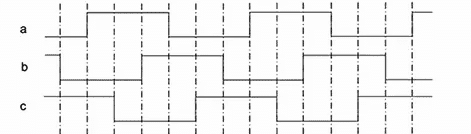 Once you have burned and confirmed the above code in your Arduino, it's time to move ahead and configure the remaining circuit stages.
For this you will need the following parts which hopefully you might have already procured:
Parts Needed
IC IR2112 - 3 nos (or any similar 3 phase driver IC)
BC547 transistors - 3 nos
capacitor 10uF/25V and 1uF/25V = 3 nos each
100uF/25V = 1no
1N4148 = 3nos (1N4148 is recommended over 1N4007)
Resistors, all 1/4 watt 5%
100 ohms = 6nos
1K = 6nos
Once you have burned and confirmed the above code in your Arduino, it's time to move ahead and configure the remaining circuit stages.
For this you will need the following parts which hopefully you might have already procured:
Parts Needed
IC IR2112 - 3 nos (or any similar 3 phase driver IC)
BC547 transistors - 3 nos
capacitor 10uF/25V and 1uF/25V = 3 nos each
100uF/25V = 1no
1N4148 = 3nos (1N4148 is recommended over 1N4007)
Resistors, all 1/4 watt 5%
100 ohms = 6nos
1K = 6nos
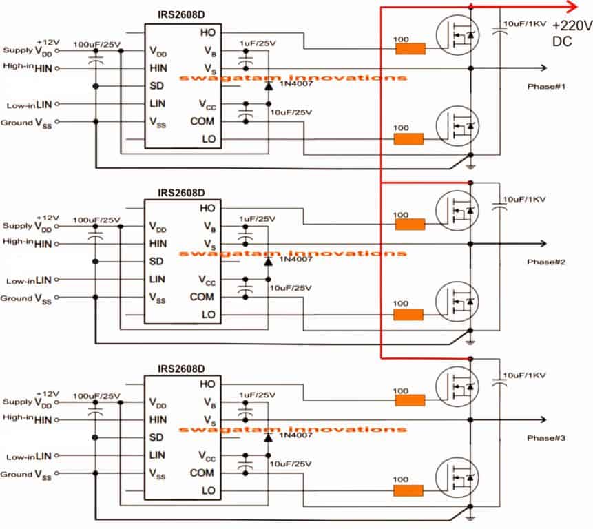 Once the driver board is assembled, the BC547 transistors are hooked up with the HIN and LIN inputs of the IC, and illustrated in the following figure:
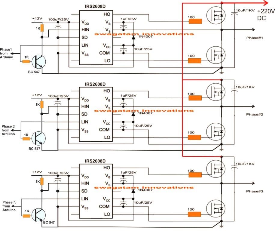 Once the above designs are constructed, the intended result could be quickly verified by switching ON the system.
Remember, the Arduino needs sometime to boot, therefore it is recommended to switch ON the Arduino first and then switch ON the +12V supply to the driver circuit after a few seconds.
Once the above designs are constructed, the intended result could be quickly verified by switching ON the system.
Remember, the Arduino needs sometime to boot, therefore it is recommended to switch ON the Arduino first and then switch ON the +12V supply to the driver circuit after a few seconds.
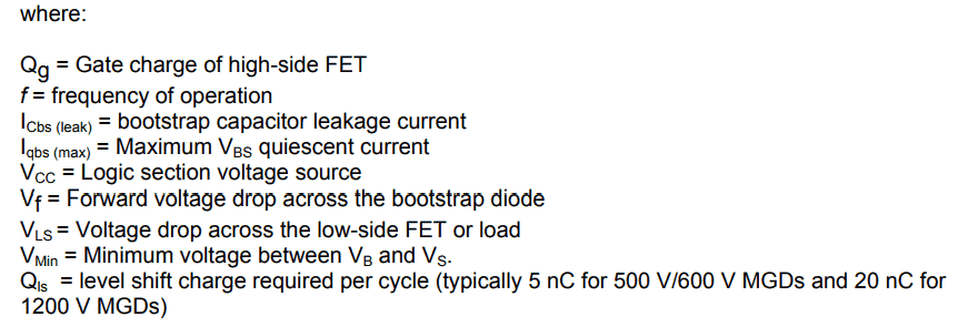
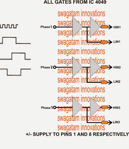
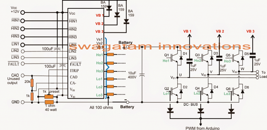 The second diagram from above forms the bridge driver stage for the proposed Arduino PWM, 3 phase inverter design, using the IC IRS2330 bridge driver chip.
The inputs of the IC indicated as HIN and LIN accept the dimensioned Arduino PWMs from the NOT gates and drives the output bridge network formed by 6 IGBTs which in turn drive the connected load across their three outputs.
The 1K preset is used for controlling the over current limit of the inverter by suitably adjusting it across the shut down pin of the I, the 1 ohm sensing resistor may be reduced appropriately if the current a relatively higher current is specified for the inverter.
Wrapping Up:
This concludes our discussion on how to build an Arduino based 3 phase inverter circuit.
If you have any further doubts or questions on this subject please feel free to comment and get the replies quickly.
For the PCB Gerber Files and other related files you can refer to the following link:
https://drive.google.com/file/d/1oAVsjNTPz6bOFaPOwu3OZPBIfDx1S3e6/view?usp=sharing
The above details were contributed by "cybrax"
The second diagram from above forms the bridge driver stage for the proposed Arduino PWM, 3 phase inverter design, using the IC IRS2330 bridge driver chip.
The inputs of the IC indicated as HIN and LIN accept the dimensioned Arduino PWMs from the NOT gates and drives the output bridge network formed by 6 IGBTs which in turn drive the connected load across their three outputs.
The 1K preset is used for controlling the over current limit of the inverter by suitably adjusting it across the shut down pin of the I, the 1 ohm sensing resistor may be reduced appropriately if the current a relatively higher current is specified for the inverter.
Wrapping Up:
This concludes our discussion on how to build an Arduino based 3 phase inverter circuit.
If you have any further doubts or questions on this subject please feel free to comment and get the replies quickly.
For the PCB Gerber Files and other related files you can refer to the following link:
https://drive.google.com/file/d/1oAVsjNTPz6bOFaPOwu3OZPBIfDx1S3e6/view?usp=sharing
The above details were contributed by "cybrax"
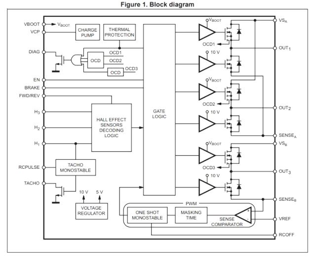 Chip Internal Structure
The chips integrates all the circuitry required for effectively driving a 3-phase BLDC motor, as explained below:
A 3-phase DMOS bridge, a constant off-time PWM current controller and the decoding logic for single ended hall sensors for generating the essential 120 degree phase shift sequence for the power stage.
With regard to the built-in protections the L6235 device offers a non-dissipative over current protection on the high-side power MOSFETs, protection against ESD, and an automatic thermal shutdown in case the device heats up above the rated value.
Chip Internal Structure
The chips integrates all the circuitry required for effectively driving a 3-phase BLDC motor, as explained below:
A 3-phase DMOS bridge, a constant off-time PWM current controller and the decoding logic for single ended hall sensors for generating the essential 120 degree phase shift sequence for the power stage.
With regard to the built-in protections the L6235 device offers a non-dissipative over current protection on the high-side power MOSFETs, protection against ESD, and an automatic thermal shutdown in case the device heats up above the rated value.
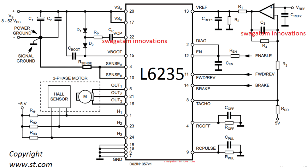 A typical L6235 50V 3-phase BLDC motor driver circuit application can be witnessed above, which looks quite straightforward with its implementation procedures.
You just have to hook up the shown elements in place and use the design to operate any BLDC motor with sensors rated within 8V to 50V at 3 amps rate.
A typical L6235 50V 3-phase BLDC motor driver circuit application can be witnessed above, which looks quite straightforward with its implementation procedures.
You just have to hook up the shown elements in place and use the design to operate any BLDC motor with sensors rated within 8V to 50V at 3 amps rate.
 Let's not waste any more time and quickly learn the main features, and specifications of this smart 3-phase driver IC.

 The figure above depicts the pinout diagram of the ICSTGIPN3H60, which is a 26 pin DIL IC, we will begin the pinout functioning explanation from the left hand side of the IC.
Pin#1: It is the ground pin of the IC and needs to be connected with the ground supply rail.
Pin#2, 15: These are the SD-OD pins, any of which can be used for shutting down the device through an external sensor circuit for safeguarding the system from a possible catastrophic situation.
A "low" signal on this pinout will execute the shut-down operation.
Pin#3, 9, 13: These are the Vcc supply voltage input pinouts, for the 3 internal driver modules and must be shorted together, and connected with a common+15V DC input.
Pin#4, 10, 14: These are the HIN inputs or the high side logic signal inputs, complementary to the LIN inputs or the Low side signal inputs.
These pinouts must be fed with a 3-phase alternating 120 degrees apart logic signals from an external source or an MCU, for initiating the motor rotation.
Pin#5, 11, 16: These are the LIN inputs or the Low side logic signal inputs, complementary to the above explained HIN inputs and should be fed with alternating 3-phase low voltage triggering signals for initiating the motor rotation.
The HIN, and LIN input signals must be anti-phase to each other, meaning whenever HIN is high, the corresponding LIN must be low and vice-versa.
Pin#6, 7, 8: These are the non-inverting, output and inverting pinouts respectively of an internal spare opamp which can be suitably configured for executing a required advanced protection circuitry in case the system demands for it, otherwise these pinouts can be left unused, however make sure not to keep these opamp inputs open and floating, rather terminate these OP+, OP- pinouts through an appropriate configuration, to prevent instability across thesepinouts.
Pin#12: It is the Cin or the comparator pin of an internal comparator stage, which facilitates processing of a sensed over-current or overload signal generated by an externally configured shunt sensing resistor.
Now let's move on to the right side of the IC and see how the indicated pinouts are designated to function and how these needs to be configured within a given driver application circuit.
Pin#19, 22, 25: These are the output pinouts of the IC, and needs to be connected straight with the specified 3-phase wires of aBLDC motor, regardless of whether the motor involves sensors or not.
A motor having sensor wires can be also used with this IC.
In case the motor incorporates hall sensors, the sensor wires could be configured with the HIN/LIN pinouts, through suitable inverting gates, because the corresponding HIN/LIN inputs must be applied with anti-phase or opposite signals for correct operation of the motor, and that's why the signals from each motor hall effect sensors must be bifurcated into+/- using NOT gates for feeding the respective HIN/LIN complementary inputs of the IC.
Pin#20, 23, 26: These pinouts are the negative supply inputs for the corresponding 3-phase motor outputs, and all these pinouts must be joined together and connected with the common ground (motor bus voltage ground and IC pin#1ground)
Pin#17, 21, 24: These are the Vboot pinouts and are required to be connected with a high voltage capacitor also referred to as bootstrap capacitor.
The 3 capacitors must be configured across these pinouts and pin#19, 22, 25 or with the corresponding outputs from the IC.
In general any 1uF/1KV capacitor can be used for these caps.
Pin#18: This pinout is the bus positive supply pin, and must be attached with the motor positive supply input, which can be anything between+12V to +600V.
The above details comprehensively explain the working, the features and the pinout specification of the compact, slim 3-phase IGBT full bridge driver ICSTGIPN3H60 from ST Microelectronics.
If you have any specific question or doubt regarding the practical implementation of this device, do not hesitate to put them forth in the below given comment box.
In a few of my upcoming articles I may additionally explain how this special 3-phase IGBT full bridge driver IC could be applied for driving high power BLDC motors, inverters, and other gadgets such as high capacity drones.
The figure above depicts the pinout diagram of the ICSTGIPN3H60, which is a 26 pin DIL IC, we will begin the pinout functioning explanation from the left hand side of the IC.
Pin#1: It is the ground pin of the IC and needs to be connected with the ground supply rail.
Pin#2, 15: These are the SD-OD pins, any of which can be used for shutting down the device through an external sensor circuit for safeguarding the system from a possible catastrophic situation.
A "low" signal on this pinout will execute the shut-down operation.
Pin#3, 9, 13: These are the Vcc supply voltage input pinouts, for the 3 internal driver modules and must be shorted together, and connected with a common+15V DC input.
Pin#4, 10, 14: These are the HIN inputs or the high side logic signal inputs, complementary to the LIN inputs or the Low side signal inputs.
These pinouts must be fed with a 3-phase alternating 120 degrees apart logic signals from an external source or an MCU, for initiating the motor rotation.
Pin#5, 11, 16: These are the LIN inputs or the Low side logic signal inputs, complementary to the above explained HIN inputs and should be fed with alternating 3-phase low voltage triggering signals for initiating the motor rotation.
The HIN, and LIN input signals must be anti-phase to each other, meaning whenever HIN is high, the corresponding LIN must be low and vice-versa.
Pin#6, 7, 8: These are the non-inverting, output and inverting pinouts respectively of an internal spare opamp which can be suitably configured for executing a required advanced protection circuitry in case the system demands for it, otherwise these pinouts can be left unused, however make sure not to keep these opamp inputs open and floating, rather terminate these OP+, OP- pinouts through an appropriate configuration, to prevent instability across thesepinouts.
Pin#12: It is the Cin or the comparator pin of an internal comparator stage, which facilitates processing of a sensed over-current or overload signal generated by an externally configured shunt sensing resistor.
Now let's move on to the right side of the IC and see how the indicated pinouts are designated to function and how these needs to be configured within a given driver application circuit.
Pin#19, 22, 25: These are the output pinouts of the IC, and needs to be connected straight with the specified 3-phase wires of aBLDC motor, regardless of whether the motor involves sensors or not.
A motor having sensor wires can be also used with this IC.
In case the motor incorporates hall sensors, the sensor wires could be configured with the HIN/LIN pinouts, through suitable inverting gates, because the corresponding HIN/LIN inputs must be applied with anti-phase or opposite signals for correct operation of the motor, and that's why the signals from each motor hall effect sensors must be bifurcated into+/- using NOT gates for feeding the respective HIN/LIN complementary inputs of the IC.
Pin#20, 23, 26: These pinouts are the negative supply inputs for the corresponding 3-phase motor outputs, and all these pinouts must be joined together and connected with the common ground (motor bus voltage ground and IC pin#1ground)
Pin#17, 21, 24: These are the Vboot pinouts and are required to be connected with a high voltage capacitor also referred to as bootstrap capacitor.
The 3 capacitors must be configured across these pinouts and pin#19, 22, 25 or with the corresponding outputs from the IC.
In general any 1uF/1KV capacitor can be used for these caps.
Pin#18: This pinout is the bus positive supply pin, and must be attached with the motor positive supply input, which can be anything between+12V to +600V.
The above details comprehensively explain the working, the features and the pinout specification of the compact, slim 3-phase IGBT full bridge driver ICSTGIPN3H60 from ST Microelectronics.
If you have any specific question or doubt regarding the practical implementation of this device, do not hesitate to put them forth in the below given comment box.
In a few of my upcoming articles I may additionally explain how this special 3-phase IGBT full bridge driver IC could be applied for driving high power BLDC motors, inverters, and other gadgets such as high capacity drones.
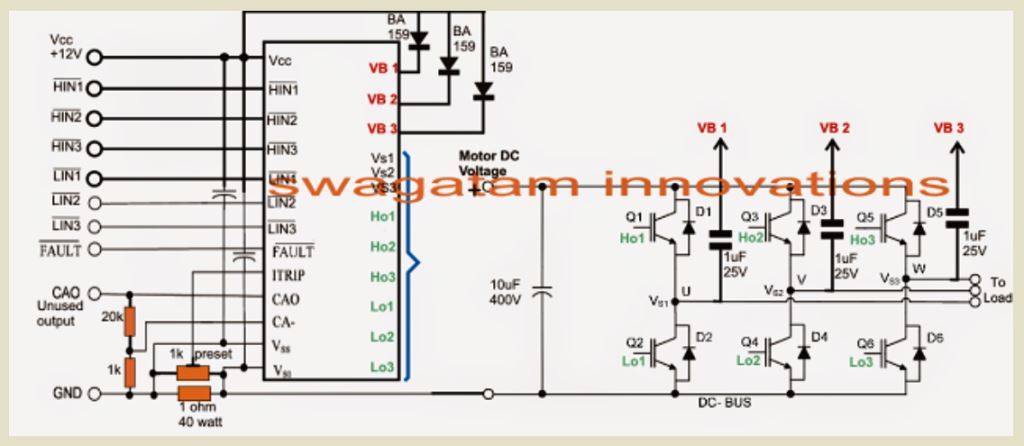 The above IC is outdated, but you can easily replace it with the latest IC 6EDL04
However since the mentioned 3 phase driver requires a dedicated 3 phase signal across its triggering inputs marked as HIN....LIN, it would be first important to learn about a simple 3 phase signal generator circuit using opamps which could be integrated with the above design for the intended outcome..
It doesn't need to be a sine wave 3 phase signals a simple square wave 120 degree phase shift PWM generator could be used for the application, as illustrated below:
The above IC is outdated, but you can easily replace it with the latest IC 6EDL04
However since the mentioned 3 phase driver requires a dedicated 3 phase signal across its triggering inputs marked as HIN....LIN, it would be first important to learn about a simple 3 phase signal generator circuit using opamps which could be integrated with the above design for the intended outcome..
It doesn't need to be a sine wave 3 phase signals a simple square wave 120 degree phase shift PWM generator could be used for the application, as illustrated below:
 The above 3 phase generator circuit can be further modified in the following manner so that it can be fed to the 3 phase driver IC shown in the first image:
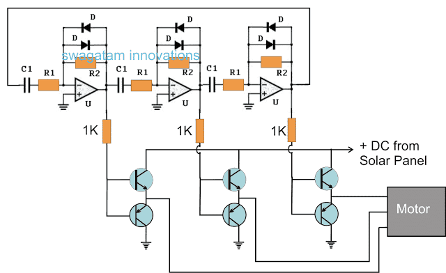 The BJTs could be replaced with appropriately rated mosfets or IGBTs...rest of the configuration is pretty straightforward and does not need much explanation.
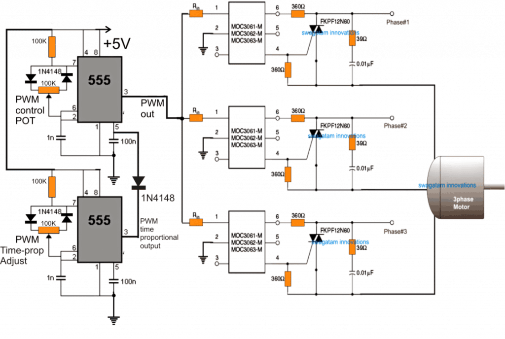 NOTE: ADDING SUITABLE INDUCTORS IN SERIES WITH THE PHASE WIRES CAN DRASTICALLY IMPROVE THE SPEED CONTROL PERFORMANCE OF THE SYSTEM.
Datasheet for MOC3061
Assumed Waveform and Phase Control using the above Concept:
NOTE: ADDING SUITABLE INDUCTORS IN SERIES WITH THE PHASE WIRES CAN DRASTICALLY IMPROVE THE SPEED CONTROL PERFORMANCE OF THE SYSTEM.
Datasheet for MOC3061
Assumed Waveform and Phase Control using the above Concept:
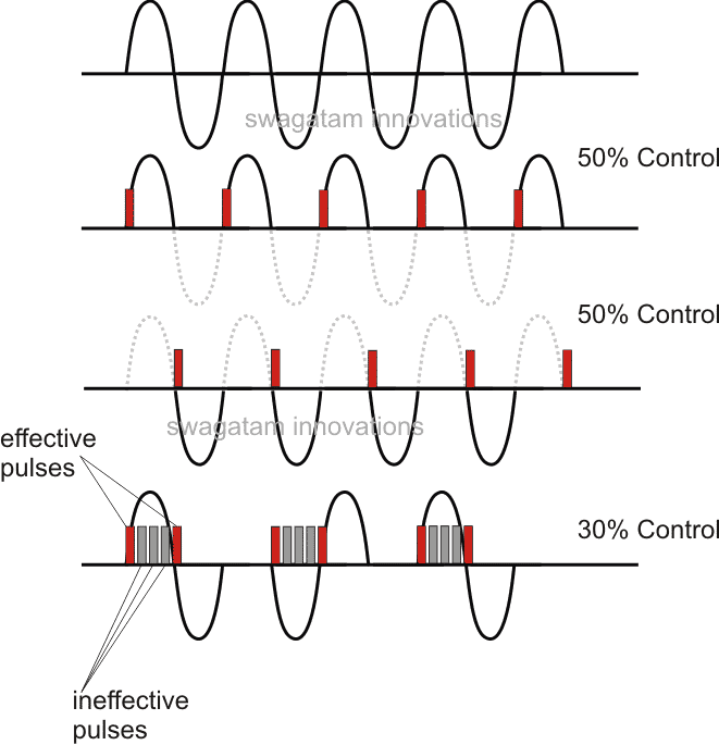 The above explained method of controlling a 3-phase induction motor is actually quite crude since it has no V/Hz control.
It simply employs switching the mains ON/OFF at different rates to produce an average power to the motor and control the speed by altering this average AC to the motor.
Imagine if you switch the motor ON/OFF manually 40 times or 50 times per minute.
That would result in your motor slowing down to some relative average value, yet moving continuously.
The above principle works in the same way.
A more technical approach is to design a circuit which ensures a proper control of the V/Hz ratio and automatically adjusts the same depending on the speed of the slip or any voltage fluctuations.
For this we basically employ the following stages:
H-Bridge or Full Bridge IGBT driver Circuit
3-Phase Generator Stage for Feeding the Full Bridge Circuit
V/Hz PWM Processor
The above explained method of controlling a 3-phase induction motor is actually quite crude since it has no V/Hz control.
It simply employs switching the mains ON/OFF at different rates to produce an average power to the motor and control the speed by altering this average AC to the motor.
Imagine if you switch the motor ON/OFF manually 40 times or 50 times per minute.
That would result in your motor slowing down to some relative average value, yet moving continuously.
The above principle works in the same way.
A more technical approach is to design a circuit which ensures a proper control of the V/Hz ratio and automatically adjusts the same depending on the speed of the slip or any voltage fluctuations.
For this we basically employ the following stages:
H-Bridge or Full Bridge IGBT driver Circuit
3-Phase Generator Stage for Feeding the Full Bridge Circuit
V/Hz PWM Processor
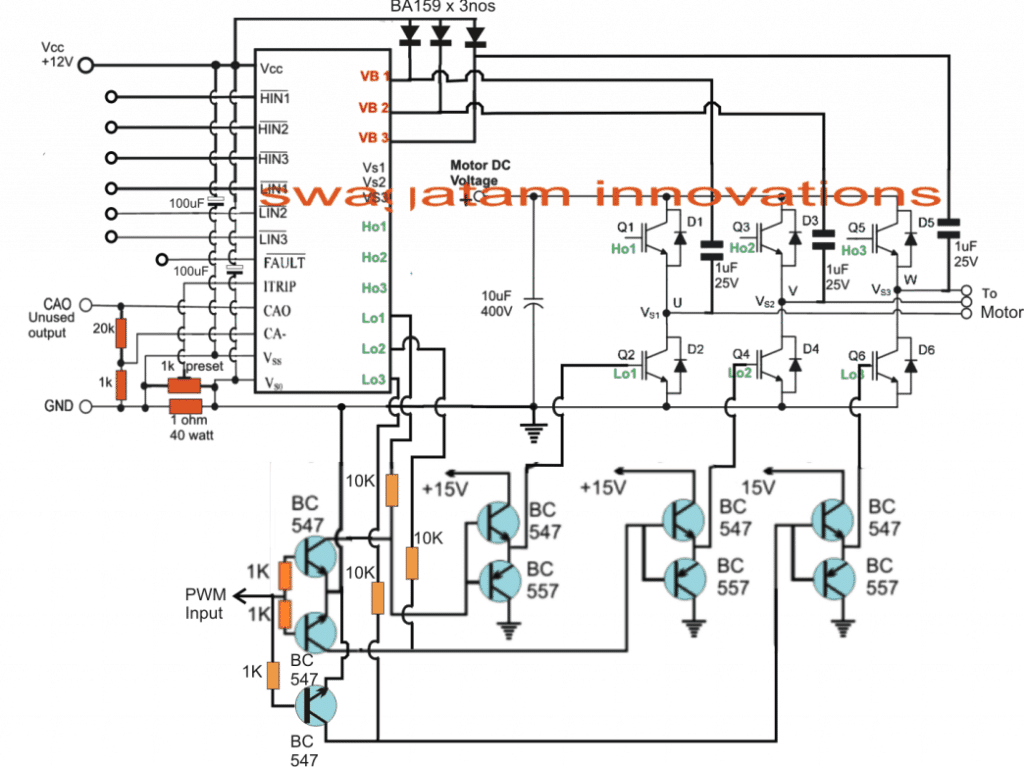 The circuit shown in the above figure utilizes a single chip full-bridge driver IC IRS2330 (latest version is 6EDL04I06NT) which has all the features in-built in order to satisfy a safe and a perfect 3 phase motor operation.
The IC only needs a synchronized 3 phase logic input across its HIN/LIN pinouts for generating the required 3 phase oscillating output, which finally is used for operating the full bridge IGBT network and the connected 3 phase motor.
The speed control PWM injection is implemented through 3 separate half bridge NPN/PNP drivers stages, controlled with a SPWM feed from an IC 555 PWM generator as seen in our previous designs.
This PWM level may be ultimately used for controlling the speed of the induction motor.
Before we learn the actual speed control method for the induction motor, let's first understand how the automatic V/Hz control can be achieved using a few IC 555 circuits, as discussed below
The circuit shown in the above figure utilizes a single chip full-bridge driver IC IRS2330 (latest version is 6EDL04I06NT) which has all the features in-built in order to satisfy a safe and a perfect 3 phase motor operation.
The IC only needs a synchronized 3 phase logic input across its HIN/LIN pinouts for generating the required 3 phase oscillating output, which finally is used for operating the full bridge IGBT network and the connected 3 phase motor.
The speed control PWM injection is implemented through 3 separate half bridge NPN/PNP drivers stages, controlled with a SPWM feed from an IC 555 PWM generator as seen in our previous designs.
This PWM level may be ultimately used for controlling the speed of the induction motor.
Before we learn the actual speed control method for the induction motor, let's first understand how the automatic V/Hz control can be achieved using a few IC 555 circuits, as discussed below
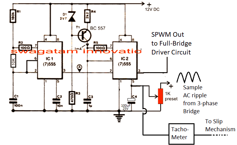 The above circuit is a simple PWM generator using a couple of IC 555.
The IC1 generates the PWM frequency which is converted into triangle waves at pin#6 of IC2 with the help of R4/C3.
These triangle waves are compared with the sinewave ripple at pin#5 of IC2. These sample ripples are acquired by rectifying the 3 phase AC mains into a 12V AC ripple and is fed to pin#5 of the IC2 for the required processing.
By comparing the two waveform, an appropriately dimensioned SPWM is generated at pin#3 of IC2, which becomes the driving PWM for the H-bridge network.
The above circuit is a simple PWM generator using a couple of IC 555.
The IC1 generates the PWM frequency which is converted into triangle waves at pin#6 of IC2 with the help of R4/C3.
These triangle waves are compared with the sinewave ripple at pin#5 of IC2. These sample ripples are acquired by rectifying the 3 phase AC mains into a 12V AC ripple and is fed to pin#5 of the IC2 for the required processing.
By comparing the two waveform, an appropriately dimensioned SPWM is generated at pin#3 of IC2, which becomes the driving PWM for the H-bridge network.
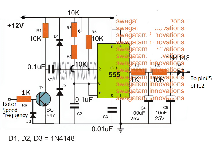
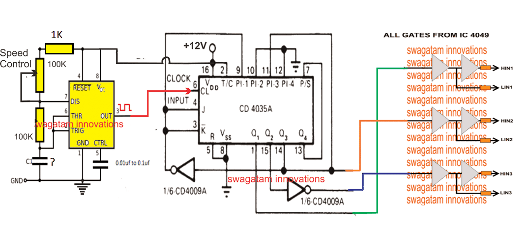 Here we can see a 3-phase generator circuit using IC 4035 whose phase shift frequency can be varied by varying the clock input at its pin#6.
The 3 phase signals are applied across the 4049 IC gates for producing the required HIN, LIN feeds for the full -bridge driver network.
This implies that by suitably varying the clock frequency of IC 4035, we can effectively change the operating 3-phase frequency of the induction motor.
This is implemented through a simple IC 555 astable circuit which feeds an adjustable frequency at pin#6 of IC 4035, and allows the frequency to be adjusted through the attached 100K pot.
The capacitor C needs to be calculated such that the adjustable frequency range comes within the correct specification of the connected induction motor.
When the frequency pot is varied, the effective frequency of the induction motor also changes, which correspondingly changes the speed of the motor.
For example when the frequency is reduced, causes the motor speed to reduce, which in turn causes the tachometer output to reduce the voltage proportionately.
This proportionate reduction in the tachometer output forces the SPWM to narrow down and thereby pulls down the voltage output to the motor proportionately.
This action in turn ensures that the V/Hz ratio is maintained while controlling the induction motor speed through frequency control.
Warning: The above concept is designed on theoretical assumptions only, please proceed with caution.
If you have any further doubts regarding this 3-phase induction motor speed controller design, you are most welcome to post the same through your comments.
Here we can see a 3-phase generator circuit using IC 4035 whose phase shift frequency can be varied by varying the clock input at its pin#6.
The 3 phase signals are applied across the 4049 IC gates for producing the required HIN, LIN feeds for the full -bridge driver network.
This implies that by suitably varying the clock frequency of IC 4035, we can effectively change the operating 3-phase frequency of the induction motor.
This is implemented through a simple IC 555 astable circuit which feeds an adjustable frequency at pin#6 of IC 4035, and allows the frequency to be adjusted through the attached 100K pot.
The capacitor C needs to be calculated such that the adjustable frequency range comes within the correct specification of the connected induction motor.
When the frequency pot is varied, the effective frequency of the induction motor also changes, which correspondingly changes the speed of the motor.
For example when the frequency is reduced, causes the motor speed to reduce, which in turn causes the tachometer output to reduce the voltage proportionately.
This proportionate reduction in the tachometer output forces the SPWM to narrow down and thereby pulls down the voltage output to the motor proportionately.
This action in turn ensures that the V/Hz ratio is maintained while controlling the induction motor speed through frequency control.
Warning: The above concept is designed on theoretical assumptions only, please proceed with caution.
If you have any further doubts regarding this 3-phase induction motor speed controller design, you are most welcome to post the same through your comments.

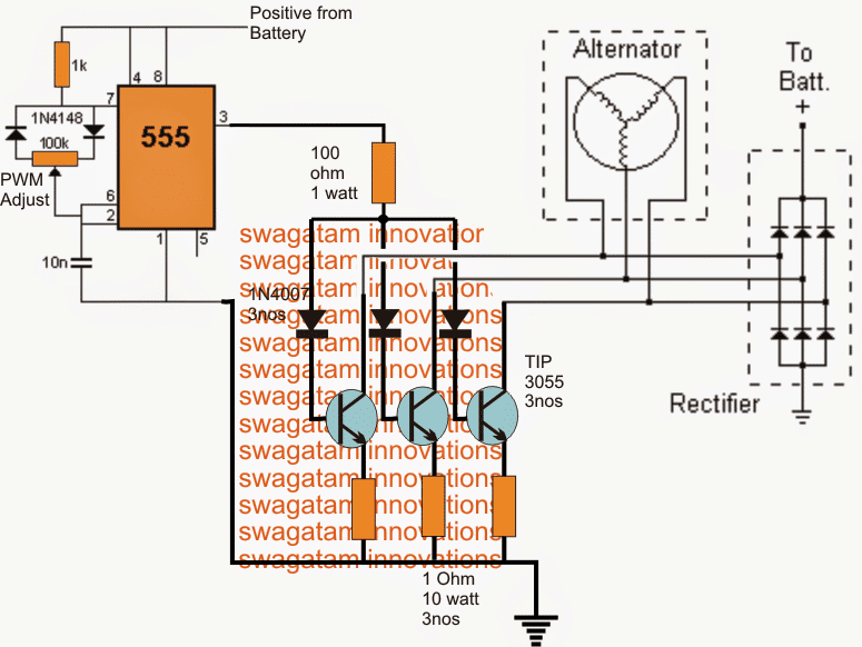 The schematic is rather easy to understand.
The 3 phase output from the alternator is sequentially applied across three power transistors which basically act like shunting devices for the alternator current.
As we all that while operating, an alternator winding could get subjected to huge reverse EMFs, to an extent which could get rip of the insulation cover of the winding destroying it permanently.
Regulating the alternator potential through the method of shunting or shorting to ground helps to keep the alternator potential under control without causing adverse effects in it.
The timing of the shunting period is crucial here and directly influences the magnitude of current that may finally reach the rectifier and the battery under charge.
A very simple way of controlling the shunting time period is by controlling the conduction of the three BJTs connected across the 3 winding of the alternator, as shown in the diagram.
Mosfets could also be used instead of the BJTs, but could be mush costlier than the BJTs.
The method is implemented by using a simple 555 IC PWM circuit.
The variable PWM output from pin3 of the IC is applied across the bases of the BJTs which in turn are forced to conduct in a controlled manner depending upon the PWM duty cycle.
The associated pot with the IC 555 circuit is appropriately adjust for obtaining the correct average RMS voltage for the battery in charge.
The method shown in the 3 phase motorcycle voltage regulator circuit using mosfets can be equally implemented for single alternators for getting identical results.
The schematic is rather easy to understand.
The 3 phase output from the alternator is sequentially applied across three power transistors which basically act like shunting devices for the alternator current.
As we all that while operating, an alternator winding could get subjected to huge reverse EMFs, to an extent which could get rip of the insulation cover of the winding destroying it permanently.
Regulating the alternator potential through the method of shunting or shorting to ground helps to keep the alternator potential under control without causing adverse effects in it.
The timing of the shunting period is crucial here and directly influences the magnitude of current that may finally reach the rectifier and the battery under charge.
A very simple way of controlling the shunting time period is by controlling the conduction of the three BJTs connected across the 3 winding of the alternator, as shown in the diagram.
Mosfets could also be used instead of the BJTs, but could be mush costlier than the BJTs.
The method is implemented by using a simple 555 IC PWM circuit.
The variable PWM output from pin3 of the IC is applied across the bases of the BJTs which in turn are forced to conduct in a controlled manner depending upon the PWM duty cycle.
The associated pot with the IC 555 circuit is appropriately adjust for obtaining the correct average RMS voltage for the battery in charge.
The method shown in the 3 phase motorcycle voltage regulator circuit using mosfets can be equally implemented for single alternators for getting identical results.
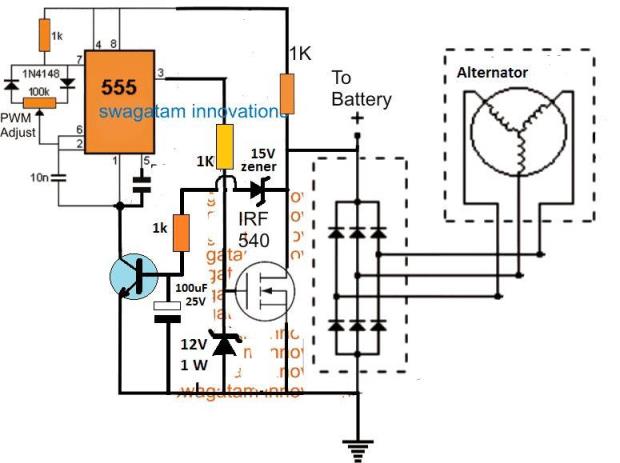 The transistor is BC547, and the pin5 capacitor is 10nF
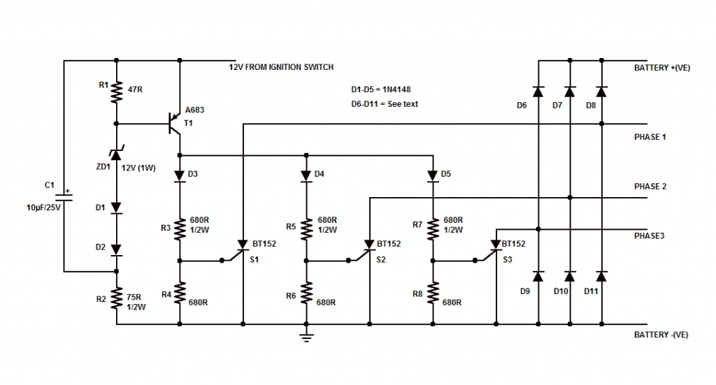
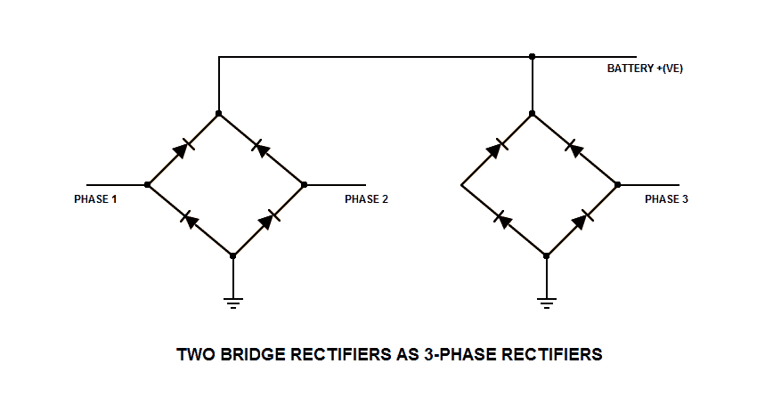

 Automotive diodes
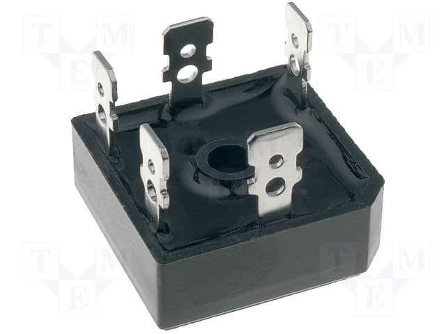
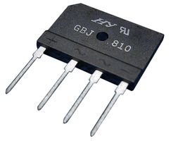
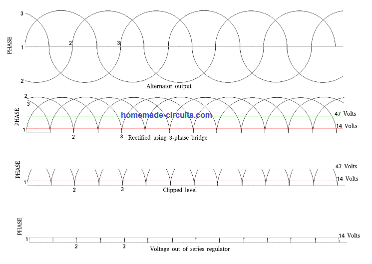 As you can see in the waveforms, there should be no capacitor needed.
But by clipping at a higher level, the current shunted to ground should be lower.
Then, dropping the voltage across a series regulatorshould not hurt anything.
There should be more than enough to keep the battery charged.
One note.
Optimum charge voltage for a lead/acid battery is actually 13.7 volts.
To hold it at 12 volts may not give the battery enough to start the engine.
And my circuit is preliminary, and still subject to change.
As you can see in the waveforms, there should be no capacitor needed.
But by clipping at a higher level, the current shunted to ground should be lower.
Then, dropping the voltage across a series regulatorshould not hurt anything.
There should be more than enough to keep the battery charged.
One note.
Optimum charge voltage for a lead/acid battery is actually 13.7 volts.
To hold it at 12 volts may not give the battery enough to start the engine.
And my circuit is preliminary, and still subject to change.
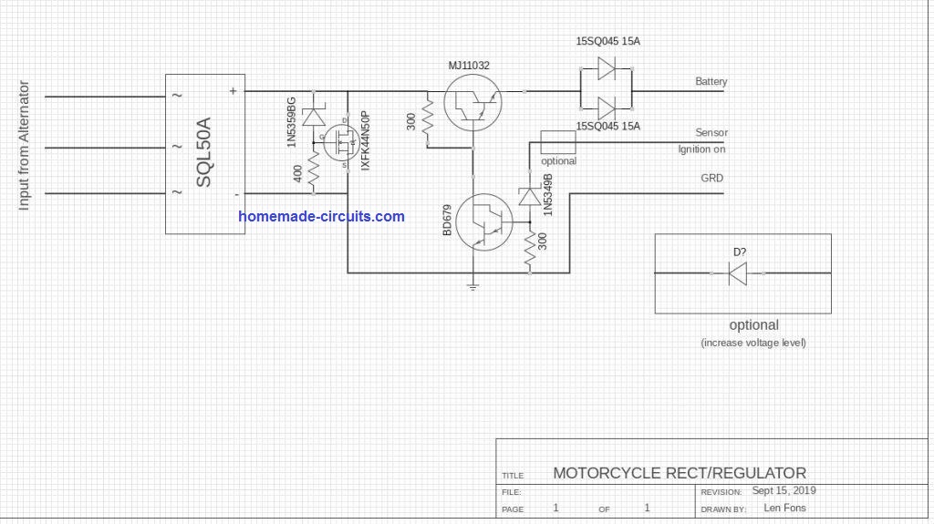 The factory looks almost primitive, in the way it works.
Their circuit charges the battery until it reaches the trigger level.
then it shunts all current to ground until the battery drops below the trigger level.
The result is a waveform with a short, harsh burst of charge that could be as high as 15 Amps.
(I did not measure it) That followed by a longer line with a slight downward slope, and another burst.
I've seen automotive batteries last 5 to 10 years, or longer.
As a kid on a farm, my father converted one of the old tractors from six volts to a twelve volt system, using an alternator from a car.
Fifteen years later, that same battery was still starting the tractor.
At the school I work with (Teaches motorcycle safety), all batteries need to be replaced within one year.
WHY ? ? ? The only thing I've been able to come up with is the charging system.
Most of the batteries I've worked with are only rated for a 2 Amp charge rate, Up to 70 volts, capable of 30 Amps, applied to the battery terminals for short bursts may be causing internal damage and shortening the life of the battery.
Especially, in the batteries where you can not check the fluid levels.
The only problem with the battery may be fluid level, but there is nothing you can do about it.
If I'm able to check and maintain fluid levels, the battery life is extended considerably.
The leads coming from the alternator would be the metric equivalent of #16. According to the AWG table, that's good for 3.7 Amps as a transmission line, and 22 Amps in chassis wiring.
On a 30 Amp alternator with a shunt regulator? The shunt level and the Amperage should be an inverse proportion, so by clipping the voltage in half, I should reduce the Amperage significantly.
In looking at the rectified waveform, the highest concentration of EMF is in the lower half.
Logic would suggest the current will be reduced to a fraction.
I'll find out when I put it into use.
On a 1500cc engine, I don't expect to notice the reduced drag on the engine, but my fuel economy may improve.
And, I remember, back when they first started putting solid-state regulators on automotive alternators, the magic number was 13.7 Volts.
However, I was planning on setting my series regulator at about 14.2 Volts.
Too high and the fluid evaporates more quickly.
You were far more helpful than you know.
Originally, I had six different circuits that I was considering and was going to breadboard each of them.
Your article eliminated five of them, so I get to save considerable time and concentrate on just one.
That saves me a good amount of work.
That makes it very well worth the time to contact you.
You have my permission to experiment with my schematic and see what you come up with.
On various forums, I'm reading where a number of people are talking about going to series regulators.Others caution against too high a voltage destroying the insulated coating on the wire.
I suspect the happy medium may be a combination of both systems, but not shunting the full output to ground.
The circuit is still simple, with few components, but not archaic.
Thank you very much for your time and attention.
One of my sources for technical information is:OCW.MIT.EDU I've been doing engineering courses there for a few years now.
You don't get any credit for doing them, but it's also completely free.
The factory looks almost primitive, in the way it works.
Their circuit charges the battery until it reaches the trigger level.
then it shunts all current to ground until the battery drops below the trigger level.
The result is a waveform with a short, harsh burst of charge that could be as high as 15 Amps.
(I did not measure it) That followed by a longer line with a slight downward slope, and another burst.
I've seen automotive batteries last 5 to 10 years, or longer.
As a kid on a farm, my father converted one of the old tractors from six volts to a twelve volt system, using an alternator from a car.
Fifteen years later, that same battery was still starting the tractor.
At the school I work with (Teaches motorcycle safety), all batteries need to be replaced within one year.
WHY ? ? ? The only thing I've been able to come up with is the charging system.
Most of the batteries I've worked with are only rated for a 2 Amp charge rate, Up to 70 volts, capable of 30 Amps, applied to the battery terminals for short bursts may be causing internal damage and shortening the life of the battery.
Especially, in the batteries where you can not check the fluid levels.
The only problem with the battery may be fluid level, but there is nothing you can do about it.
If I'm able to check and maintain fluid levels, the battery life is extended considerably.
The leads coming from the alternator would be the metric equivalent of #16. According to the AWG table, that's good for 3.7 Amps as a transmission line, and 22 Amps in chassis wiring.
On a 30 Amp alternator with a shunt regulator? The shunt level and the Amperage should be an inverse proportion, so by clipping the voltage in half, I should reduce the Amperage significantly.
In looking at the rectified waveform, the highest concentration of EMF is in the lower half.
Logic would suggest the current will be reduced to a fraction.
I'll find out when I put it into use.
On a 1500cc engine, I don't expect to notice the reduced drag on the engine, but my fuel economy may improve.
And, I remember, back when they first started putting solid-state regulators on automotive alternators, the magic number was 13.7 Volts.
However, I was planning on setting my series regulator at about 14.2 Volts.
Too high and the fluid evaporates more quickly.
You were far more helpful than you know.
Originally, I had six different circuits that I was considering and was going to breadboard each of them.
Your article eliminated five of them, so I get to save considerable time and concentrate on just one.
That saves me a good amount of work.
That makes it very well worth the time to contact you.
You have my permission to experiment with my schematic and see what you come up with.
On various forums, I'm reading where a number of people are talking about going to series regulators.Others caution against too high a voltage destroying the insulated coating on the wire.
I suspect the happy medium may be a combination of both systems, but not shunting the full output to ground.
The circuit is still simple, with few components, but not archaic.
Thank you very much for your time and attention.
One of my sources for technical information is:OCW.MIT.EDU I've been doing engineering courses there for a few years now.
You don't get any credit for doing them, but it's also completely free.
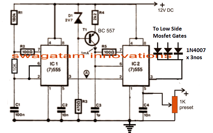
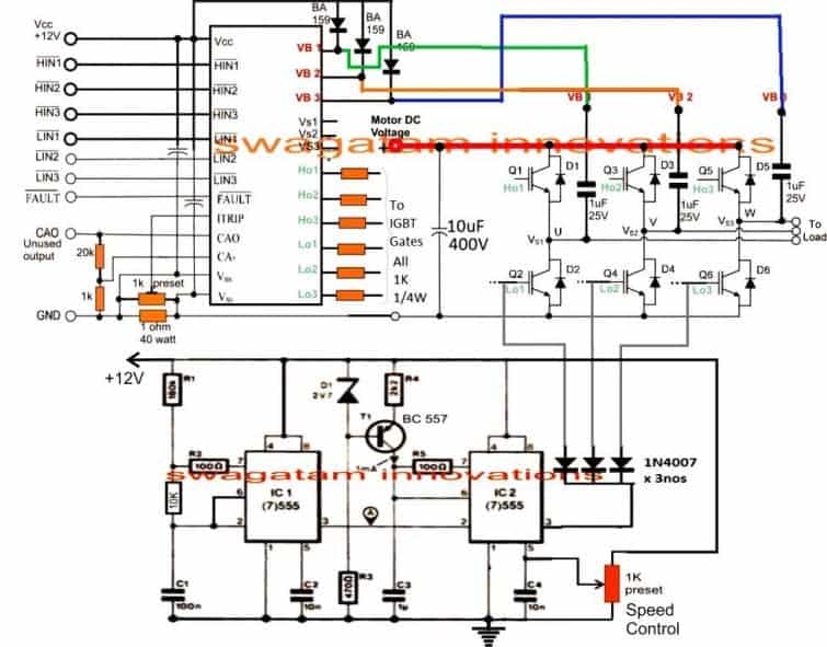 In the following diagram we visualize the required 3 phase signal generator circuit.
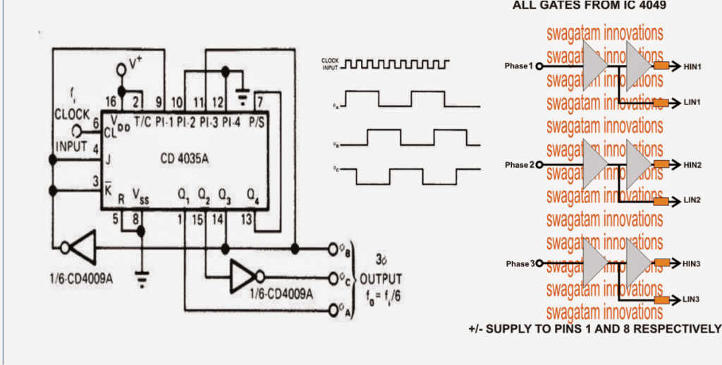
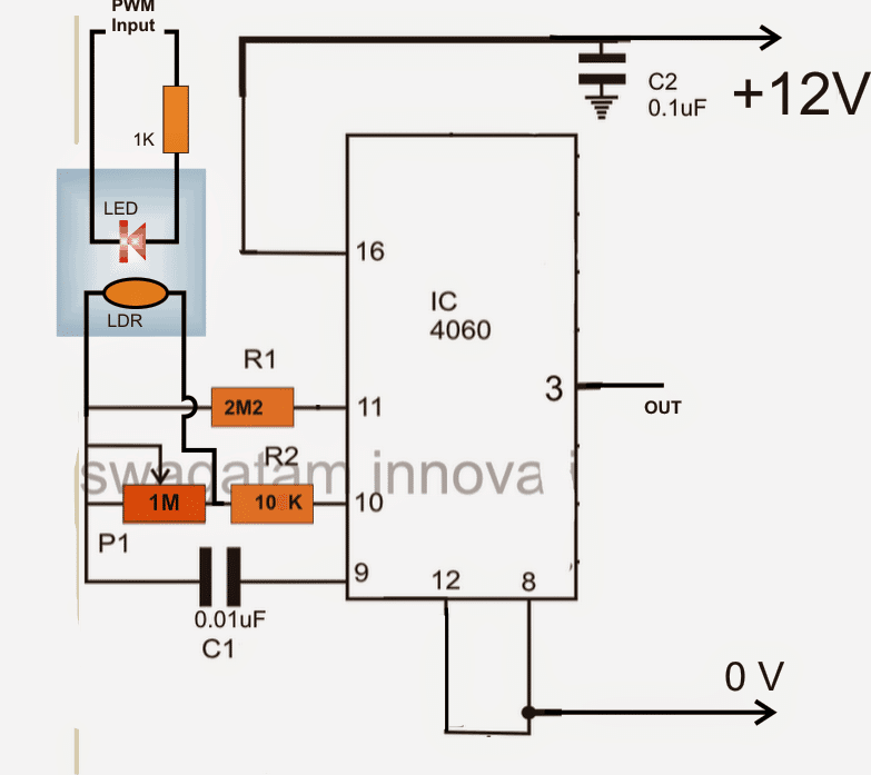 In the above voltage to frequency converter circuit a IC 4060 is used and its frequency dependent resistance is influenced through a LED/LDR assembly for the intended conversions.
The LED/LDR assembly is sealed inside a light proof box, and the LDR is positioned across a 1M frequency dependent resistor of the IC.
Since the LDR/LDR response is fairly linear, the varying illumination of the LED on the LDR generates a proportionately varying (increasing or decreasing) frequency across pin3 of the IC.
The FSD or the V/Hz range of the stage could be set by appropriately setting up the 1M resistor or even the C1 value.
The LED is voltage is derived and illuminated through the PWMs from the first PWM circuit stage.
It implies that as the PWMs vary, the LED illumination will also vary which in turn would give rise to a proportionately increasing or decreasing frequency at pin3 of the IC 4060 in the above diagram.
In the above voltage to frequency converter circuit a IC 4060 is used and its frequency dependent resistance is influenced through a LED/LDR assembly for the intended conversions.
The LED/LDR assembly is sealed inside a light proof box, and the LDR is positioned across a 1M frequency dependent resistor of the IC.
Since the LDR/LDR response is fairly linear, the varying illumination of the LED on the LDR generates a proportionately varying (increasing or decreasing) frequency across pin3 of the IC.
The FSD or the V/Hz range of the stage could be set by appropriately setting up the 1M resistor or even the C1 value.
The LED is voltage is derived and illuminated through the PWMs from the first PWM circuit stage.
It implies that as the PWMs vary, the LED illumination will also vary which in turn would give rise to a proportionately increasing or decreasing frequency at pin3 of the IC 4060 in the above diagram.
 For a single phase source the rectification may be implemented using standard 4 diode bridge network configuration.
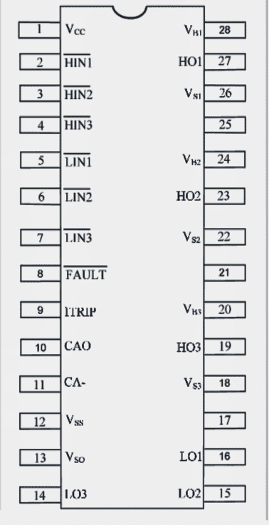
 The above shows the pinout diagram of the IC IRS2330 which simply needs to be connected to a set of a few external components for implementing the proposed BLDC controller circuit.
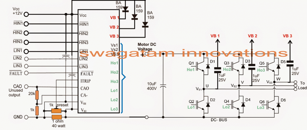
 Before applying the hall sensor triggers to the driver IC inputs, it's required to be buffered through a couple of NOT gates as given in the diagram above.
Finally, the outputs of the NOT gates is integrated appropriately with the inputs of the IC IRS2330.
The negatives of all the hall sensors may be assumed to be grounded.
The second circuit which forms the main driver configuration for the proposed 3 phase brushless BLDC motor driver circuit, could be also seen having a current sensing stage across its lower left section.
The resistive divider may be appropriately dimensioned for enabling an over current protection and control over the connected BLDC motor.
For getting comprehensive details regarding the current sensing configuration and other intricacies of the whole design, one may refer to the following datasheet of the IC:
https://www.irf.com/product-info/datasheets/data/irs2330pbf.pdf
Before applying the hall sensor triggers to the driver IC inputs, it's required to be buffered through a couple of NOT gates as given in the diagram above.
Finally, the outputs of the NOT gates is integrated appropriately with the inputs of the IC IRS2330.
The negatives of all the hall sensors may be assumed to be grounded.
The second circuit which forms the main driver configuration for the proposed 3 phase brushless BLDC motor driver circuit, could be also seen having a current sensing stage across its lower left section.
The resistive divider may be appropriately dimensioned for enabling an over current protection and control over the connected BLDC motor.
For getting comprehensive details regarding the current sensing configuration and other intricacies of the whole design, one may refer to the following datasheet of the IC:
https://www.irf.com/product-info/datasheets/data/irs2330pbf.pdf
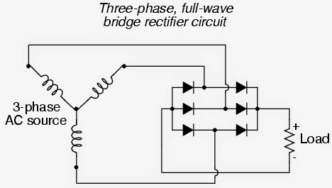 Now, once the 3 phase rectified DC is achieved, this will need to be converted to the desired single phase AC, as per the request this value should be 220 V.
A full bridge mosfet driver topology may be incorporated for implementing the above requirement, as shown in the following diagram:
Now, once the 3 phase rectified DC is achieved, this will need to be converted to the desired single phase AC, as per the request this value should be 220 V.
A full bridge mosfet driver topology may be incorporated for implementing the above requirement, as shown in the following diagram:
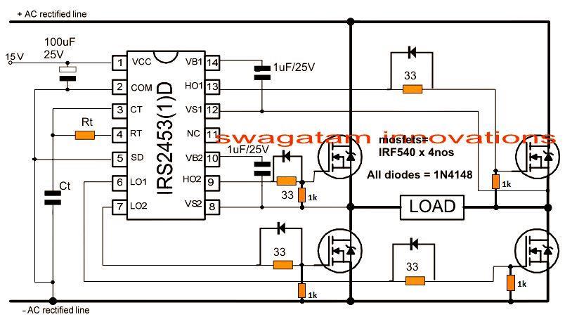 The layout looks simple and easy to configure, however it would produce and subject the load to the full 530 V instead of the specified 220 V.
The issue can be normalized and controlled to the desired levels through an external voltage sensor circuit, which could be further integrated with the Ct pin of the IC IRS2453.
The simple solution can be implemented by incorporating the following circuit:
The layout looks simple and easy to configure, however it would produce and subject the load to the full 530 V instead of the specified 220 V.
The issue can be normalized and controlled to the desired levels through an external voltage sensor circuit, which could be further integrated with the Ct pin of the IC IRS2453.
The simple solution can be implemented by incorporating the following circuit:
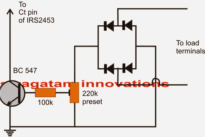 The 220k preset is adjusted precisely so that the transistor just begins conducting at voltages around 240 V across the load.
When the transistor conducts, the Ct pin is grounded at that instant, forcing the IC to inhibit its oscillations which in turn renders the high side outputs to go low, cutting off the rectified high voltage to the mosfets.
This results in lowering down of the voltage across the load which allows the BC547 to switch OFF and restore the IC operations....the procedure repeats making sure that the output stays under control and at the specified 220 V level.
The 220k preset is adjusted precisely so that the transistor just begins conducting at voltages around 240 V across the load.
When the transistor conducts, the Ct pin is grounded at that instant, forcing the IC to inhibit its oscillations which in turn renders the high side outputs to go low, cutting off the rectified high voltage to the mosfets.
This results in lowering down of the voltage across the load which allows the BC547 to switch OFF and restore the IC operations....the procedure repeats making sure that the output stays under control and at the specified 220 V level.
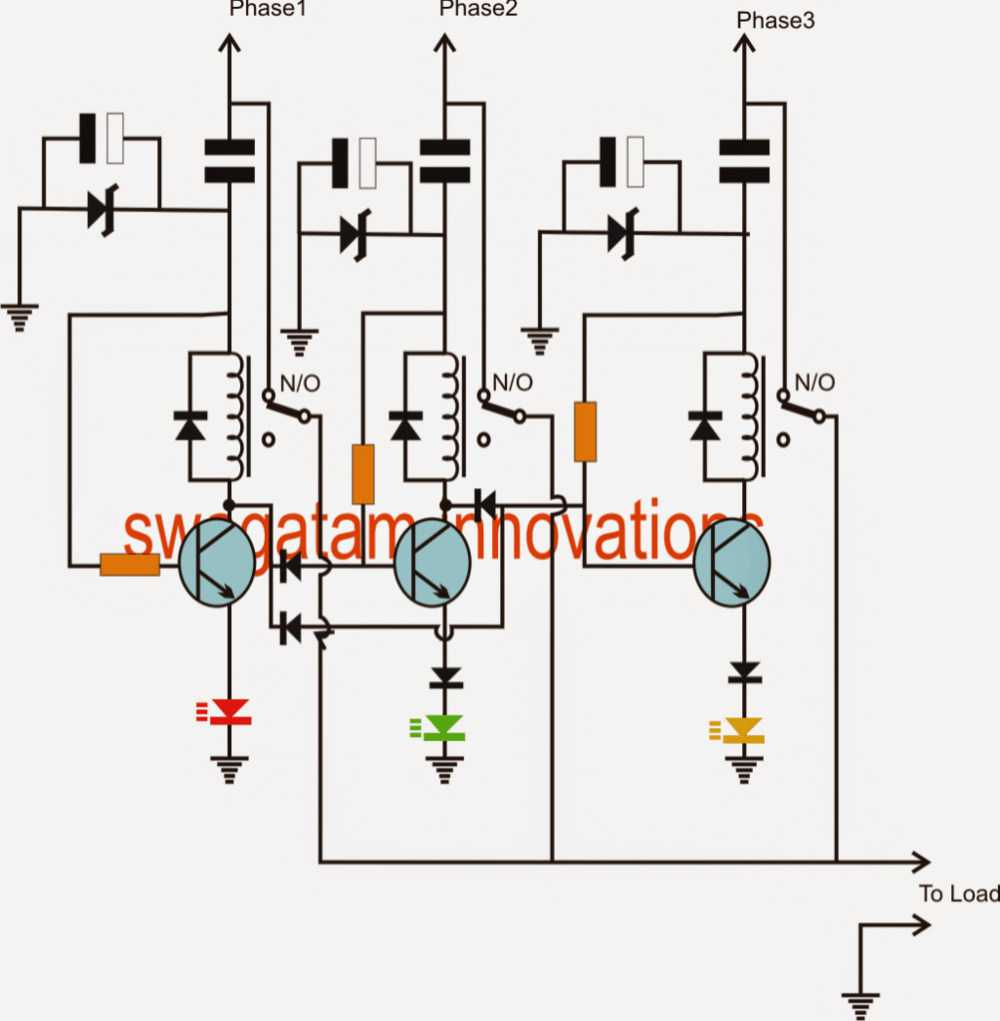
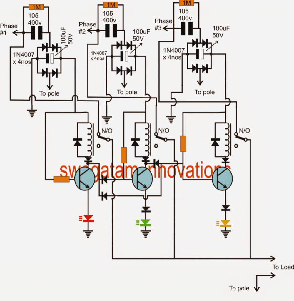
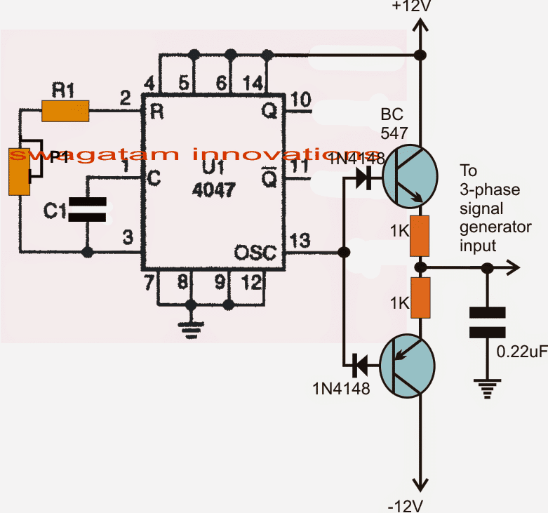 The followingcircuitshows a simple three phase generator circuit which converters the above input push-pull signal into 3 discrete outputs, phase shifted by 120 degrees.
These outputs are further bifurcated by individual push-pull stages made from a NOT gates stages.
These 3 discrete 120 degree phase shifted, push pull PWMs now become the feeding input signals (HIN, LIN) for the final 3 phase driver stage explained below.
This signal generator uses a single 12V supply and not a dual supply.
Complete explanation can be found in this 3 phase signal generator article
The followingcircuitshows a simple three phase generator circuit which converters the above input push-pull signal into 3 discrete outputs, phase shifted by 120 degrees.
These outputs are further bifurcated by individual push-pull stages made from a NOT gates stages.
These 3 discrete 120 degree phase shifted, push pull PWMs now become the feeding input signals (HIN, LIN) for the final 3 phase driver stage explained below.
This signal generator uses a single 12V supply and not a dual supply.
Complete explanation can be found in this 3 phase signal generator article
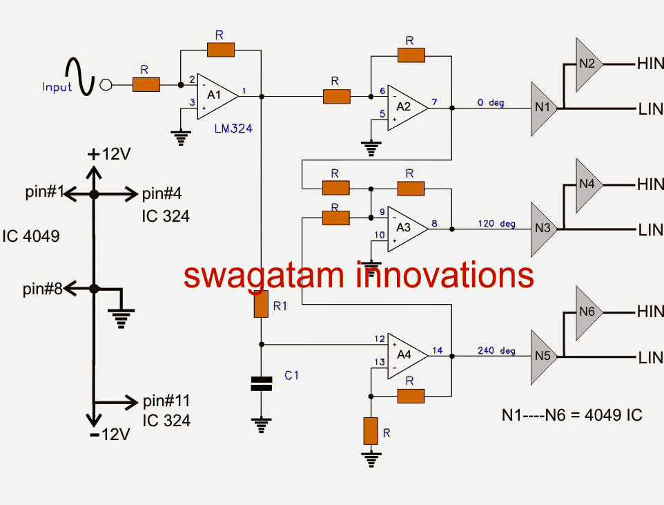 The circuit below shows a 3 phase inverter inverter circuit stage using H-bridge mosfets configuration which receives the phase shifted PWMs from the above stage and converts them into corresponding high voltage AC outputs for operating the connected 3 phase load, normally this would be a 3 phase motor.
The 330 high voltage across the indivdual mosfet drivers sections is obtained from any standard single phase inverter integrated across the shownmosfets drains for powering the desired 3 phase load.
The circuit below shows a 3 phase inverter inverter circuit stage using H-bridge mosfets configuration which receives the phase shifted PWMs from the above stage and converts them into corresponding high voltage AC outputs for operating the connected 3 phase load, normally this would be a 3 phase motor.
The 330 high voltage across the indivdual mosfet drivers sections is obtained from any standard single phase inverter integrated across the shownmosfets drains for powering the desired 3 phase load.
 In the above 3 phase generator circuit (second last diagram) using a sine wave doesn't make sense because the 4049 would ultimately convert it into square waves, and moreover the driver ICs in the last design employ digital ICs which will not respond to sine waves.
Therefore a better idea is to use a 3 phase square wave signal generator for feeding the last driver stage.
You may refer the article which explains how to make a 3 phase solar inverter circuit for understanding the 3 phase signal generator stage functioning and implementation details.
In the above 3 phase generator circuit (second last diagram) using a sine wave doesn't make sense because the 4049 would ultimately convert it into square waves, and moreover the driver ICs in the last design employ digital ICs which will not respond to sine waves.
Therefore a better idea is to use a 3 phase square wave signal generator for feeding the last driver stage.
You may refer the article which explains how to make a 3 phase solar inverter circuit for understanding the 3 phase signal generator stage functioning and implementation details.
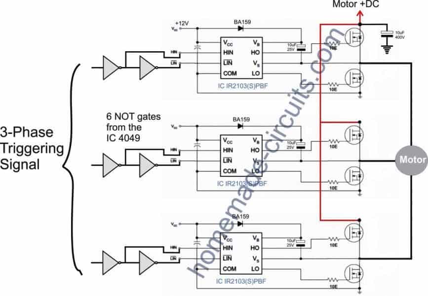
 Therefore now you can simply replace the earlier explained IC 4047 and the opamp section entirely and integrate this design with HIN, LIN inputs f the 3 phase driver circuit.
But remember you will have to still use the N1----N6 gates between this new circuit and the full bridge driver circuit.
Therefore now you can simply replace the earlier explained IC 4047 and the opamp section entirely and integrate this design with HIN, LIN inputs f the 3 phase driver circuit.
But remember you will have to still use the N1----N6 gates between this new circuit and the full bridge driver circuit.
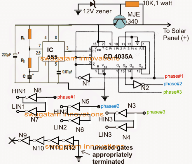
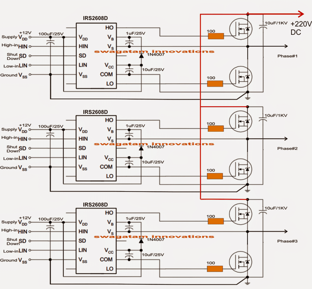 Note: The shut down pin must be connectedto the ground line if not used, otherwise the circuit will not work
As may be seen in the above figure, this section is built across 3 separate half bridge driver ICs using IRS2608 which are specialized for driving high side and low side mosfet pairs.
The configuration looks quite straightforward, thanks to this highly sophisticated driver IC from International rectifier.
Each IC stage has its own HIN (high In) and LIN (low In) input pins and also their respective supply Vcc/ground pins.
All the Vcc are required to be joined together and connected with the 12V supply line of the first circuit (pin4/8 of IC555), so that all the circuit stages become accessible to the 12V supply derived from the solar panel.
Similarly all the ground pins and lines must be made into a common rail.
The HIN and LIN should be joined with the outputs generated from the NOT gates as specified in the second diagram.
The above arrangement takes care of the 3 phase processing and amplification, however since the 3 phase output should be at the mains level and a solar panel could be rated at a maximum of 60V, we must have an arrangement that would enable boosting this low 60 volts solar panel to the required 220V or 120V level.
Note: The shut down pin must be connectedto the ground line if not used, otherwise the circuit will not work
As may be seen in the above figure, this section is built across 3 separate half bridge driver ICs using IRS2608 which are specialized for driving high side and low side mosfet pairs.
The configuration looks quite straightforward, thanks to this highly sophisticated driver IC from International rectifier.
Each IC stage has its own HIN (high In) and LIN (low In) input pins and also their respective supply Vcc/ground pins.
All the Vcc are required to be joined together and connected with the 12V supply line of the first circuit (pin4/8 of IC555), so that all the circuit stages become accessible to the 12V supply derived from the solar panel.
Similarly all the ground pins and lines must be made into a common rail.
The HIN and LIN should be joined with the outputs generated from the NOT gates as specified in the second diagram.
The above arrangement takes care of the 3 phase processing and amplification, however since the 3 phase output should be at the mains level and a solar panel could be rated at a maximum of 60V, we must have an arrangement that would enable boosting this low 60 volts solar panel to the required 220V or 120V level.
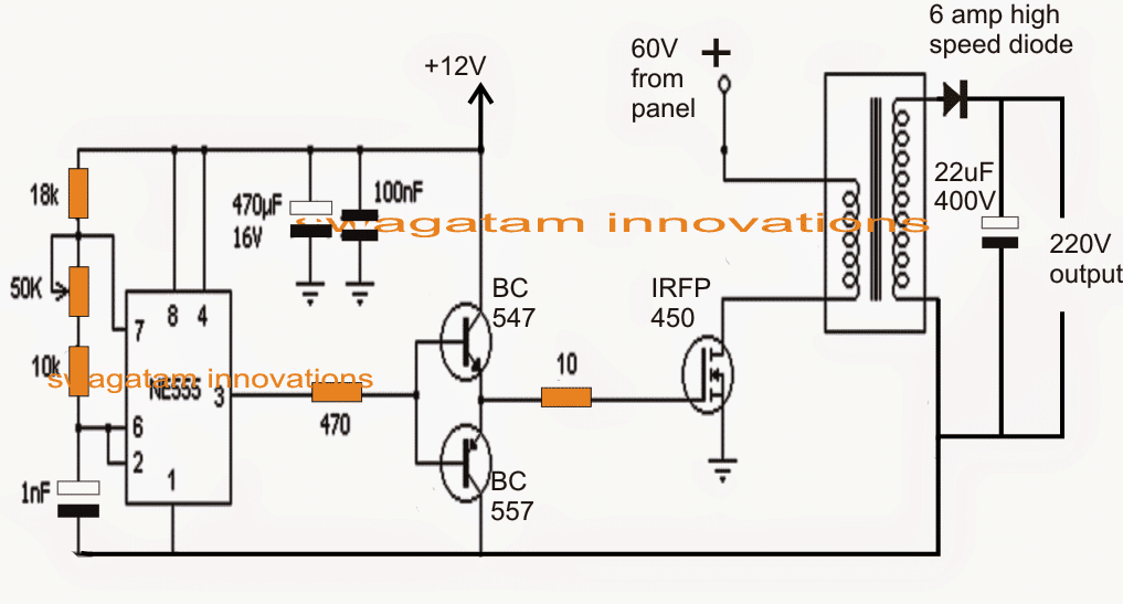 Again, the shown configuration of the 60V to 220V boost converter looks not so difficult, and can be constructed using very ordinary components.
The IC 555 is configured as an astable with a frequency of approximately 20 to 50 kHz.
This frequency is fed to the gate of a switching mosfet via a push pull BJT stage.
The heart of the boost circuit is formed with the help of a compact ferrite core transformer which receives the driving frequency from the mosfet and converter the 60V input into the required 220V output.
This 220V DC is finally attached with the previously explained mosfet driver stage across the drains of the 3 phase mosfets for achieving the 220V 3 phase output.
The boost converter transformer can be built on any suitable EE core/bobbin assembly using 1mm 50 turns primary (two 0.5mm bifilar magnet wire in parallel), and secondary using o.5 mm magnet wire with 200 turns
Again, the shown configuration of the 60V to 220V boost converter looks not so difficult, and can be constructed using very ordinary components.
The IC 555 is configured as an astable with a frequency of approximately 20 to 50 kHz.
This frequency is fed to the gate of a switching mosfet via a push pull BJT stage.
The heart of the boost circuit is formed with the help of a compact ferrite core transformer which receives the driving frequency from the mosfet and converter the 60V input into the required 220V output.
This 220V DC is finally attached with the previously explained mosfet driver stage across the drains of the 3 phase mosfets for achieving the 220V 3 phase output.
The boost converter transformer can be built on any suitable EE core/bobbin assembly using 1mm 50 turns primary (two 0.5mm bifilar magnet wire in parallel), and secondary using o.5 mm magnet wire with 200 turns
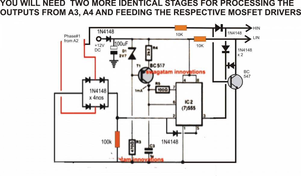
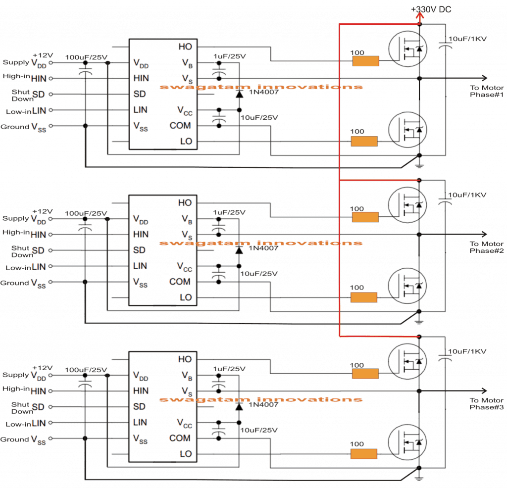
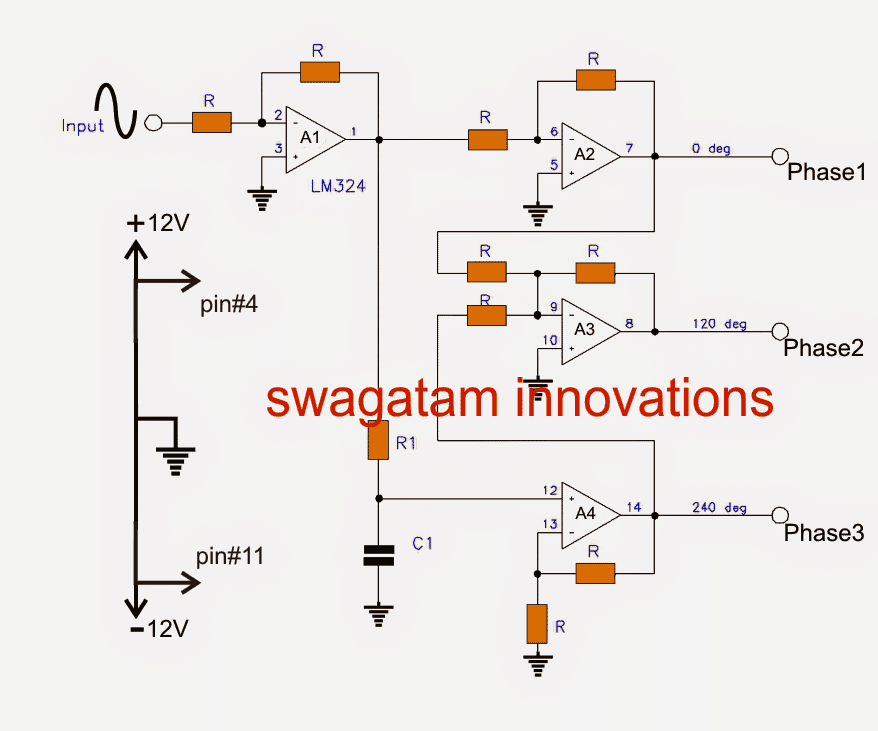
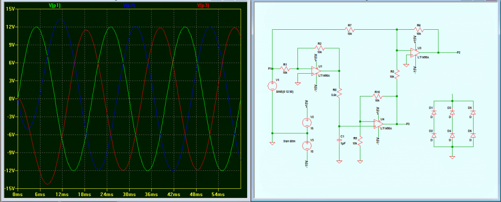 However, my actual requirement could not be fulfilled.
When these 3 phases are connected to a 3-phase rectifier, the wave form of phase 2 and 3 gets disturbed.
I tried with the original circuit, in that case all three phases gets disturbed
However, my actual requirement could not be fulfilled.
When these 3 phases are connected to a 3-phase rectifier, the wave form of phase 2 and 3 gets disturbed.
I tried with the original circuit, in that case all three phases gets disturbed
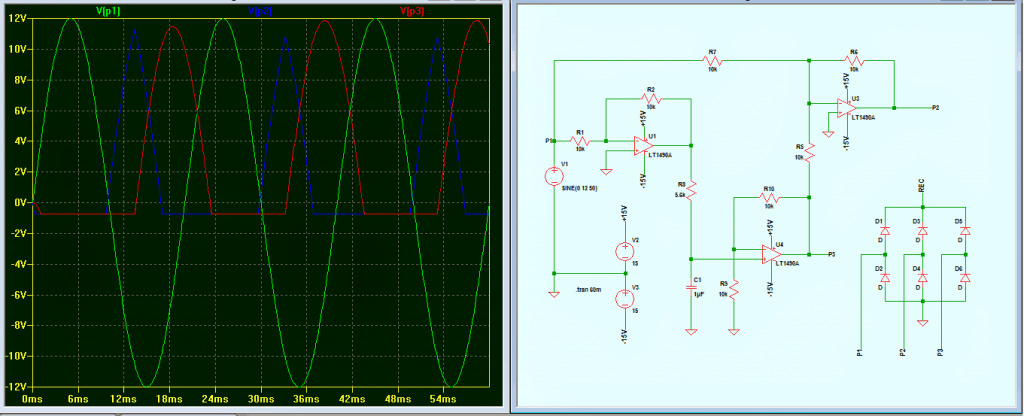 Finally got a solution! A 100nF capacitor connected in series with each phase and the rectifier solved the problem to a great extent.
Though the rectified output is not consistent but, it is quite acceptable
Finally got a solution! A 100nF capacitor connected in series with each phase and the rectifier solved the problem to a great extent.
Though the rectified output is not consistent but, it is quite acceptable
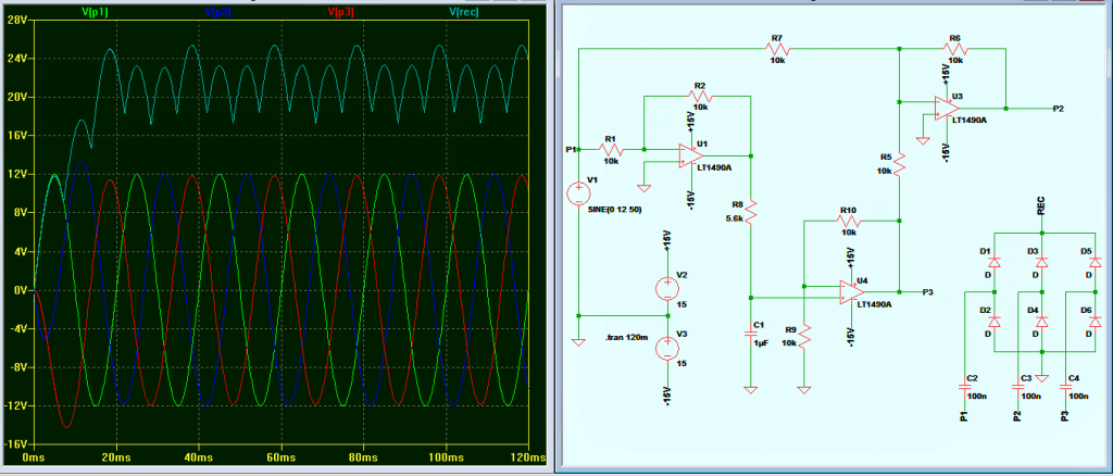 Update:The following image shows a much simpler alternative for generating 3 phase signals with accuracy and without complicated adjustments:

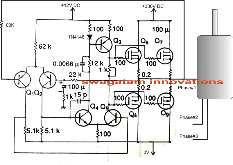
 This is also a delay relay ON timer circuit but it works with a DC input derived from the amplifier SMPS or power supply.
When the amplifier is switched ON, the delay timer is also switched ON from the amplifier's supply.
However, being a delay ON timer, the relay does not respond immediately rather waits for sometime depending on the values of R1, R2, C2. Once the set time elapses, the relay activates and connects the amplifier output with the loudspeakers.
The slight delay in switching allows the amplifier circuit to settle down adequately, ans switch ON the loudspeaker safely, thus preventing the fuses from sudden over current.
Parts List
R1 = 100K
R2 = 100K
R3, R4 = 10K
D2, D3 = 1N4007
C2 = 100uF/25V
T1 = BC547
T2 = BC557
Relay = 12 V relay, 10 amps.
This is also a delay relay ON timer circuit but it works with a DC input derived from the amplifier SMPS or power supply.
When the amplifier is switched ON, the delay timer is also switched ON from the amplifier's supply.
However, being a delay ON timer, the relay does not respond immediately rather waits for sometime depending on the values of R1, R2, C2. Once the set time elapses, the relay activates and connects the amplifier output with the loudspeakers.
The slight delay in switching allows the amplifier circuit to settle down adequately, ans switch ON the loudspeaker safely, thus preventing the fuses from sudden over current.
Parts List
R1 = 100K
R2 = 100K
R3, R4 = 10K
D2, D3 = 1N4007
C2 = 100uF/25V
T1 = BC547
T2 = BC557
Relay = 12 V relay, 10 amps.
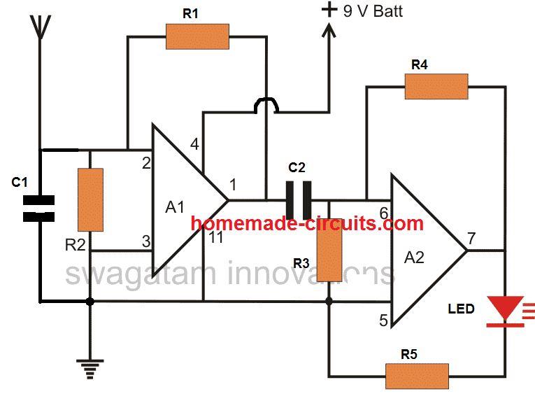 NOTE: the sensitivity of the circuit can be adjusted to much higher levels either by increasing the 2M2 resistor value, or by adding two more op amp stages in series with the above design, since we already have two extra op amps in spare inside the IC.
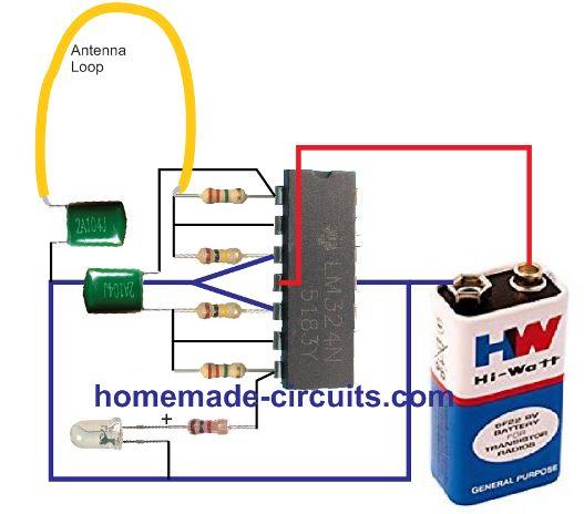
 A high impedance ground network intended for wide band detection is supplied by R3. Having inductor L1 hooked up to the circuit by means of S2, the circuit gets adjusted for the FM band.
Diodes D1 and D2 perform the job of detection and demodulation.
The detected RF signal is transferred to the non-inverting input of op amp IC1 .
The IC1 op amp is constructed like a non-inverting amplifier through a preset gain of approximately 450. The circuit works by using junction field effect transistors (JFETs) at the input sections; which boosts sensitivity because of their high impedance.
Potentiometer R9 works like a squelch control which tunes the IC1 offset settings.
The amplified detector output which shows up on pin 6 of IC1 is transferred to J1.
An appropriate high impedance phone could be attached to J1 whenever you would like to hear the detected signal.
Furthermore, R6 and C6 do the job of cleaning the signal.
The cleaned up signal is subsequently given to the input of IC2, which is an LM3914 dot /bar display chip.
The LM3914 or LM3915 device includes a network of resistor and a range of comparators.
With respect to the input voltage fed to pin 5, several LEDs will probably light up to show the relative voltage levels.
In this RF sniffer circuit, a 9 LED bar display is set up by attaching pin 3 of the IC2 with the positive supply voltage.
When the detected signal is the weakest, this might illuminate only the LED#9. As the detected signal voltage becomes stronger, each of the LEDs in the bar graph turns on one by one until, with the most powerful RF signal level, you might find all the nine LEDs being illuminated.
Resistors R7 and R8 are used to fix the reference voltage for a full-scale bar graph LED display.
Observe that we have not used any current-limiting resistors for the LEDs; since the resistors R7 and R8 itself fulfill the function of limiting the LED current.
A high impedance ground network intended for wide band detection is supplied by R3. Having inductor L1 hooked up to the circuit by means of S2, the circuit gets adjusted for the FM band.
Diodes D1 and D2 perform the job of detection and demodulation.
The detected RF signal is transferred to the non-inverting input of op amp IC1 .
The IC1 op amp is constructed like a non-inverting amplifier through a preset gain of approximately 450. The circuit works by using junction field effect transistors (JFETs) at the input sections; which boosts sensitivity because of their high impedance.
Potentiometer R9 works like a squelch control which tunes the IC1 offset settings.
The amplified detector output which shows up on pin 6 of IC1 is transferred to J1.
An appropriate high impedance phone could be attached to J1 whenever you would like to hear the detected signal.
Furthermore, R6 and C6 do the job of cleaning the signal.
The cleaned up signal is subsequently given to the input of IC2, which is an LM3914 dot /bar display chip.
The LM3914 or LM3915 device includes a network of resistor and a range of comparators.
With respect to the input voltage fed to pin 5, several LEDs will probably light up to show the relative voltage levels.
In this RF sniffer circuit, a 9 LED bar display is set up by attaching pin 3 of the IC2 with the positive supply voltage.
When the detected signal is the weakest, this might illuminate only the LED#9. As the detected signal voltage becomes stronger, each of the LEDs in the bar graph turns on one by one until, with the most powerful RF signal level, you might find all the nine LEDs being illuminated.
Resistors R7 and R8 are used to fix the reference voltage for a full-scale bar graph LED display.
Observe that we have not used any current-limiting resistors for the LEDs; since the resistors R7 and R8 itself fulfill the function of limiting the LED current.
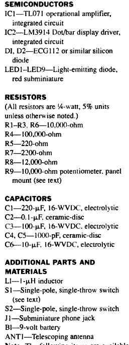 For further inquiries or information please use the comment box below.

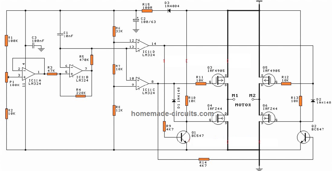 HOW IT FUNCTIONS (refer to schematic)
The circuit could be divided in four stages:
1. Motor control �C IC1:A
2. Triangle wave generator �C IC1:B
3. Voltage comparators �C IC1:C and D
4. Motor drive �C Q3-6
Let us get started with the motor driver stage, centered around MOSFETs Q3-6. Only a couple of these MOSFETs remain in the activated state at any instant of time.
While Q3 and Q6 are ON current moves through the motor and causes it to rotate in a single direction.
As soon as Q4 and Q5 are in operating condition the current circulation is reversed and the motor starts rotating in the opposite direction.
IC1:C and IC1:D deal with which MOSFETs are switched on.
Opamps IC1:C and IC1:D are wired as voltage comparators.
The reference voltage for these opamps are produced by the resistor voltage divider of R6, R7 and R8.
Observe that the reference voltage for IC1:D is attached tothe ��+�� input but for IC1:C it is coupled to the ��-�� input.
This means IC1:D is activated with a voltage higher than its reference whereas IC1:C is prompted with a voltage lower than its reference.
Opamp IC1:B is configured as a triangle wave generator and supplies the activation signal to the relevant voltage comparators.
The frequency is roughly the inverse of the time constant of R5 and C1 �C 270Hz for the values employed.
Decreasing R5 or C1 increases the frequency; increasing either of these is going to reduce the frequency.The peak-to-peak output level of the triangle wave is much less than the difference between the two voltage references.
It is therefore extremely hard for both comparators to be activated at the same time.
Or else all 4 MOSFETs would begin conducting, leading to a short circuit and ruining all of them.
The triangle waveform is structured around a DC offset voltage.
Increasing or decreasing the offset voltage varies the pulse position of the triangle wave appropriately.
Switching the triangle wave upward enables comparator IC1:D to activate; decreasing it results in comparator IC1:C to activate.
When the voltage level of the triangle wave is in the middle of the two voltage references then none of the comparators are induced.The DC offset voltage is regulated by the potentiometer P1 via IC1:A, that is designed as a voltage follower.
This gives a low output impedance voltage source,allowing the DC offset voltage to be less vulnerable to the loading impact of IC1:B.
As the ��pot�� is switched the DC offset voltage begins varying, either up or down based on the direction the pot is flipped.Diode D3 presents reverse polarity safeguard for the controller.
Resistor R15 and capacitor C2 are a simple low pass filter.
This is meant to clean any voltage spikes brought on by the MOSFETs as they turn ON supply power to the motor.
Parts List
HOW IT FUNCTIONS (refer to schematic)
The circuit could be divided in four stages:
1. Motor control �C IC1:A
2. Triangle wave generator �C IC1:B
3. Voltage comparators �C IC1:C and D
4. Motor drive �C Q3-6
Let us get started with the motor driver stage, centered around MOSFETs Q3-6. Only a couple of these MOSFETs remain in the activated state at any instant of time.
While Q3 and Q6 are ON current moves through the motor and causes it to rotate in a single direction.
As soon as Q4 and Q5 are in operating condition the current circulation is reversed and the motor starts rotating in the opposite direction.
IC1:C and IC1:D deal with which MOSFETs are switched on.
Opamps IC1:C and IC1:D are wired as voltage comparators.
The reference voltage for these opamps are produced by the resistor voltage divider of R6, R7 and R8.
Observe that the reference voltage for IC1:D is attached tothe ��+�� input but for IC1:C it is coupled to the ��-�� input.
This means IC1:D is activated with a voltage higher than its reference whereas IC1:C is prompted with a voltage lower than its reference.
Opamp IC1:B is configured as a triangle wave generator and supplies the activation signal to the relevant voltage comparators.
The frequency is roughly the inverse of the time constant of R5 and C1 �C 270Hz for the values employed.
Decreasing R5 or C1 increases the frequency; increasing either of these is going to reduce the frequency.The peak-to-peak output level of the triangle wave is much less than the difference between the two voltage references.
It is therefore extremely hard for both comparators to be activated at the same time.
Or else all 4 MOSFETs would begin conducting, leading to a short circuit and ruining all of them.
The triangle waveform is structured around a DC offset voltage.
Increasing or decreasing the offset voltage varies the pulse position of the triangle wave appropriately.
Switching the triangle wave upward enables comparator IC1:D to activate; decreasing it results in comparator IC1:C to activate.
When the voltage level of the triangle wave is in the middle of the two voltage references then none of the comparators are induced.The DC offset voltage is regulated by the potentiometer P1 via IC1:A, that is designed as a voltage follower.
This gives a low output impedance voltage source,allowing the DC offset voltage to be less vulnerable to the loading impact of IC1:B.
As the ��pot�� is switched the DC offset voltage begins varying, either up or down based on the direction the pot is flipped.Diode D3 presents reverse polarity safeguard for the controller.
Resistor R15 and capacitor C2 are a simple low pass filter.
This is meant to clean any voltage spikes brought on by the MOSFETs as they turn ON supply power to the motor.
Parts List


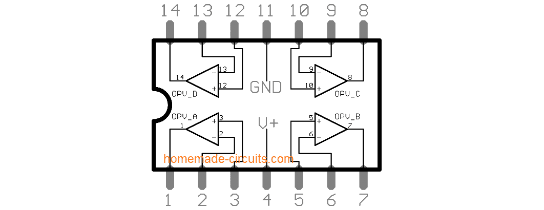
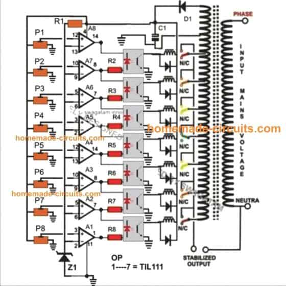
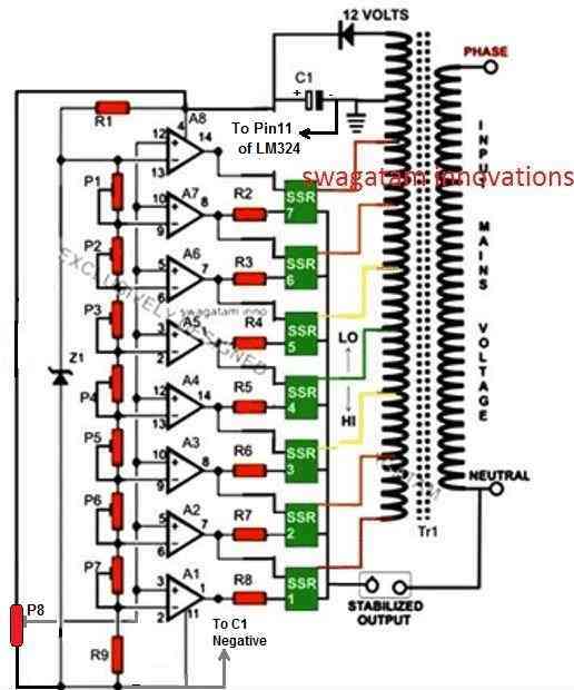
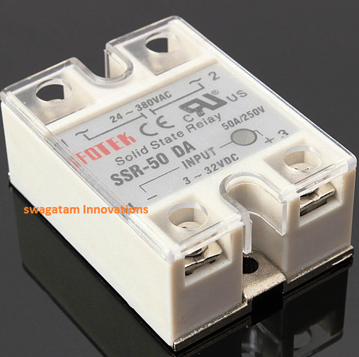
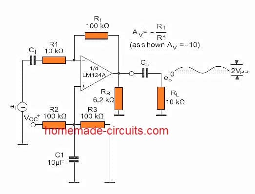 DC summing Amplifier:
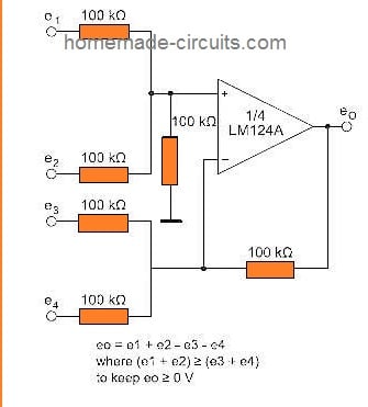 Non Inverting DC Gain:
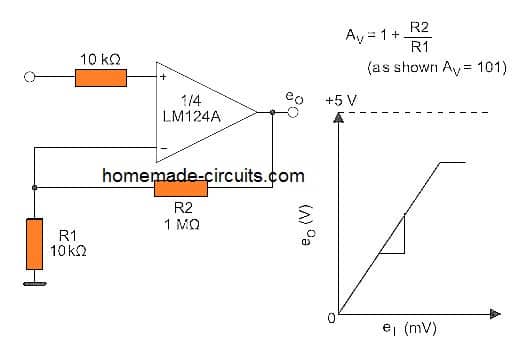 Feel free to report any errors or questions via comment section you may get a quick reply.

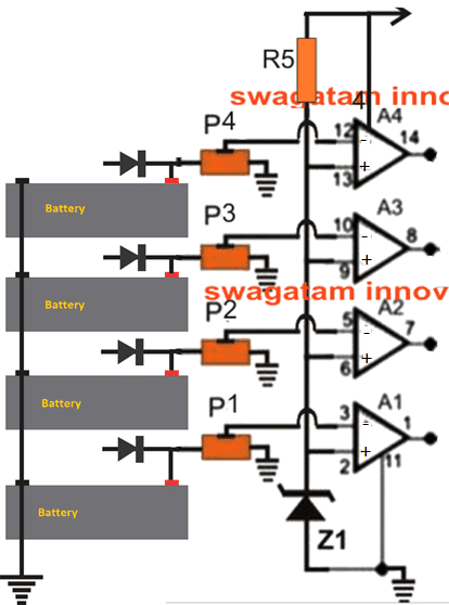 Parts List:
opamps: LM324
presets:10K
zener 6V/0.5 watt
R5 = 10K
diodes = 6A4 or as per the charging specs
We will consider only 4 batteries here, and therefore use 4 opamps for the respective over charge cut offs.
A1 to A4 opamps are taken from the quad opamp IC LM324, each configured as compartaors to detect the attached corresponding battery over charge levels.
As can be seen in the diagram the non-inverting inputs of each of the opamps is configured with the relevant battery positives for enabling the required sensing of the battery voltages.
The positives of the individual batteries are connected with the capacitor dump output, which we will discuss in the later part of the article.
The inverting (-) pins of the opamps are designated to a fixed reference level through a single common zener diode.
The presets attached with the (+) or the non-inverting inputs of the opamps and are used for setting up the precise full-charge trip points with respect to the corresponding (-) pin zener reference levels.
The presets are set such that when the relevant battery voltage reaches the full charge level, the proportionate value at the pin(+) of the opamp just goes above the (-) pin zener reference level.
The above situation instantly turns the opamp's output from its initial 0V to a high logic equal to the supply voltage level.
This high at the opamp output triggers an IC 555 atable circuit so that the IC 555 is enabled to produce a periodic ON/OFF intervals over the attached capacitor dump circuit...the following discussion will explain us the proceedings:
Parts List:
opamps: LM324
presets:10K
zener 6V/0.5 watt
R5 = 10K
diodes = 6A4 or as per the charging specs
We will consider only 4 batteries here, and therefore use 4 opamps for the respective over charge cut offs.
A1 to A4 opamps are taken from the quad opamp IC LM324, each configured as compartaors to detect the attached corresponding battery over charge levels.
As can be seen in the diagram the non-inverting inputs of each of the opamps is configured with the relevant battery positives for enabling the required sensing of the battery voltages.
The positives of the individual batteries are connected with the capacitor dump output, which we will discuss in the later part of the article.
The inverting (-) pins of the opamps are designated to a fixed reference level through a single common zener diode.
The presets attached with the (+) or the non-inverting inputs of the opamps and are used for setting up the precise full-charge trip points with respect to the corresponding (-) pin zener reference levels.
The presets are set such that when the relevant battery voltage reaches the full charge level, the proportionate value at the pin(+) of the opamp just goes above the (-) pin zener reference level.
The above situation instantly turns the opamp's output from its initial 0V to a high logic equal to the supply voltage level.
This high at the opamp output triggers an IC 555 atable circuit so that the IC 555 is enabled to produce a periodic ON/OFF intervals over the attached capacitor dump circuit...the following discussion will explain us the proceedings:

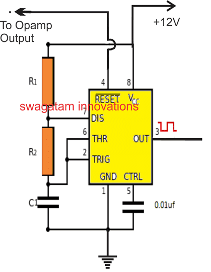 Parts List
IC = IC 555
R2 = 22K
R1, C2 = calculate to get the desired charge dump cycle rate
As shown in the above diagram, pin#4 which is the reset pinout of the IC 555 is connected with the output of the relevant opamp stage.
Each of the opamps will have its own separate IC 555 stages along with the capacitor dump circuit stage.
While the battery is in the charging process and the opamp output is held at zero, the IC 555 astable stays disabled, however the moment the relevant attached battery gets fully charged, and the concerned opamp output turns positive, the connected the IC 555 astable becomes activated, which causes its output pin#3 to generate a periodic ON/OFF cycles.
The pin#3 of the IC 555 is configured with its own individual capacitor dump circuit, which responds to the ON/OFF cycles from the IC 555 stage and begins the process of charging and dumping a capacitor across the relevant battery.
To understand how this dump capacitor behaves in response to the IC 555 ON/OFF cycles we may have to go through the following section of the article:
Parts List
IC = IC 555
R2 = 22K
R1, C2 = calculate to get the desired charge dump cycle rate
As shown in the above diagram, pin#4 which is the reset pinout of the IC 555 is connected with the output of the relevant opamp stage.
Each of the opamps will have its own separate IC 555 stages along with the capacitor dump circuit stage.
While the battery is in the charging process and the opamp output is held at zero, the IC 555 astable stays disabled, however the moment the relevant attached battery gets fully charged, and the concerned opamp output turns positive, the connected the IC 555 astable becomes activated, which causes its output pin#3 to generate a periodic ON/OFF cycles.
The pin#3 of the IC 555 is configured with its own individual capacitor dump circuit, which responds to the ON/OFF cycles from the IC 555 stage and begins the process of charging and dumping a capacitor across the relevant battery.
To understand how this dump capacitor behaves in response to the IC 555 ON/OFF cycles we may have to go through the following section of the article:

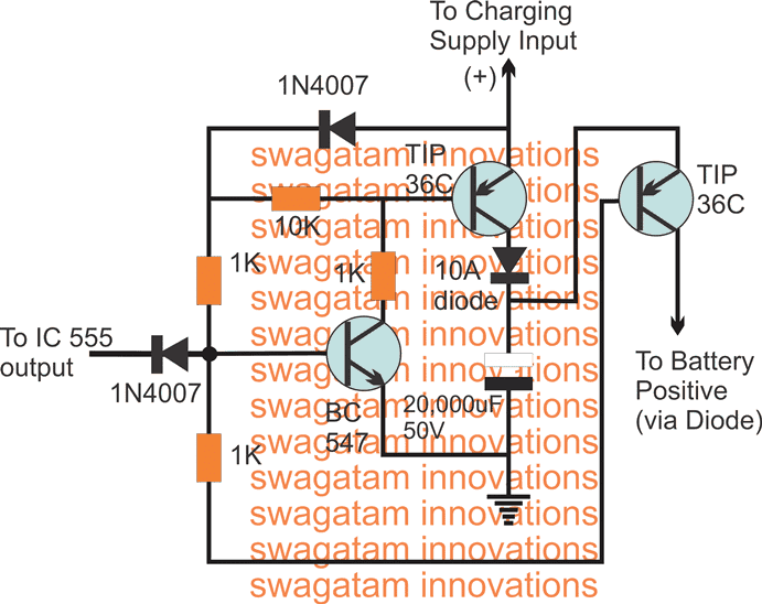 The circuit functioning of the above shown capacitor dump charger circuit can be learned following explanation:
As long as IC 555 stays in the disabled state, the BC547 is allowed to get the required biasing through its base 1K resistor, which in turn keeps the associated TIP36 transistor in the ON position.
This situation allows the high value collector capacitor to get charged to its maximum allowable limit.
In this position the capacitor is armed in the charged stand-by position.
The moment IC 555 stage gets activated and begins its ON OFF cycle, the OFF periods of the cycle switches OFF BC547/TIP36 pair, and switches ON the extreme left side TIP36, which instantly closes and dumps the charge from the capacitor into the associated battery positive.
The next ON cycle from the IC 555 reverts the situation into the previous conditions and charges the 20,000uF capacitor, and yet again, with the next subsequent OFF cycle the capacitor is allowed to dump its charge via the relevant TIP36 transistor.
This charging and dumping operation is carried out continuously until the corresponding battery becomes fully charged, forcing the opamp to turn OFF itself and the whole proceedings.
All the opamps work in the similar manner, by sensing the attached battery condition and self starting the above explained procedures.
This concludes the explanation regarding the proposed automatic multiple battery charger using capacitor dump charging, if you have any questions or doubts, do not hesitate to communicate through comments...
The circuit functioning of the above shown capacitor dump charger circuit can be learned following explanation:
As long as IC 555 stays in the disabled state, the BC547 is allowed to get the required biasing through its base 1K resistor, which in turn keeps the associated TIP36 transistor in the ON position.
This situation allows the high value collector capacitor to get charged to its maximum allowable limit.
In this position the capacitor is armed in the charged stand-by position.
The moment IC 555 stage gets activated and begins its ON OFF cycle, the OFF periods of the cycle switches OFF BC547/TIP36 pair, and switches ON the extreme left side TIP36, which instantly closes and dumps the charge from the capacitor into the associated battery positive.
The next ON cycle from the IC 555 reverts the situation into the previous conditions and charges the 20,000uF capacitor, and yet again, with the next subsequent OFF cycle the capacitor is allowed to dump its charge via the relevant TIP36 transistor.
This charging and dumping operation is carried out continuously until the corresponding battery becomes fully charged, forcing the opamp to turn OFF itself and the whole proceedings.
All the opamps work in the similar manner, by sensing the attached battery condition and self starting the above explained procedures.
This concludes the explanation regarding the proposed automatic multiple battery charger using capacitor dump charging, if you have any questions or doubts, do not hesitate to communicate through comments...
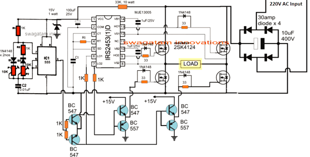 The first idea as indicated above employs an IRS2453 full bridge inverter circuit and an attached IC 555 PWM controller stage for the intended RPM control of a diesel generator output.
The design looks pretty straightforward, wherein the diode bridge network converts the 220V input to a 330V DC bus voltage for the full bridge driver network, which in turn converts it into a 220V AC square wave through the associated 4 N-channel push pull mosfet network.
Since this output is 330V DC square wave output, it is appropriately processed using the IC 555 PWM section into the required 220V AC sine wave output.The PWM setting ensures a fixed 220V output which can e expected to be relatively stble without fluctuations.
The first idea as indicated above employs an IRS2453 full bridge inverter circuit and an attached IC 555 PWM controller stage for the intended RPM control of a diesel generator output.
The design looks pretty straightforward, wherein the diode bridge network converts the 220V input to a 330V DC bus voltage for the full bridge driver network, which in turn converts it into a 220V AC square wave through the associated 4 N-channel push pull mosfet network.
Since this output is 330V DC square wave output, it is appropriately processed using the IC 555 PWM section into the required 220V AC sine wave output.The PWM setting ensures a fixed 220V output which can e expected to be relatively stble without fluctuations.
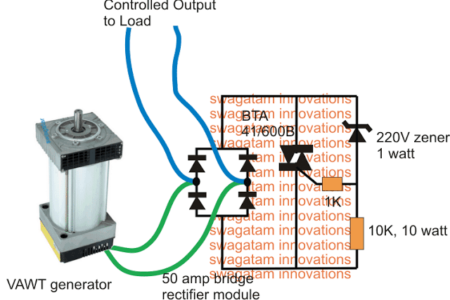 The above circuit was originally designed for controlling a windmill VAWT motor
However the same design could be also effectively used for controlling a diesel generator output to a fixed 220V.
The circuit looks much simpler and self explanatory.
The bridge rectifier converts both the half cycles from the diesel generator into positive full wave cycles for the triac, so that the triac circuit is able to shunt both these cycles to ground that may exceed the 220V mark.
The 220v zener diode fixes the shunting level for the triac, this section could be replaced using TL431 shunt zener IC for enabling an accurate temperature stabilized output for the generator.The bridge network must be adequately rated to handle the generator current peaks.
The above circuit was originally designed for controlling a windmill VAWT motor
However the same design could be also effectively used for controlling a diesel generator output to a fixed 220V.
The circuit looks much simpler and self explanatory.
The bridge rectifier converts both the half cycles from the diesel generator into positive full wave cycles for the triac, so that the triac circuit is able to shunt both these cycles to ground that may exceed the 220V mark.
The 220v zener diode fixes the shunting level for the triac, this section could be replaced using TL431 shunt zener IC for enabling an accurate temperature stabilized output for the generator.The bridge network must be adequately rated to handle the generator current peaks.
 As we can infer from the above diagram, each keys are connected to one row and one column.
When any one of them are depressed, for instance number 1, R1 and C1 gets connected, this signal will be received by arduino or any microcontroller and determine which key is pressed, for each key, unique connections are made.
We can get 4x4 keypad from e-commerce website or local electronics retailer or you can make one from the diagram above.
You just need 16 push buttons for 4x4 keypad and a general purpose PCB.
The connections can be made from the above diagram and you made one for yourself.
As we can infer from the above diagram, each keys are connected to one row and one column.
When any one of them are depressed, for instance number 1, R1 and C1 gets connected, this signal will be received by arduino or any microcontroller and determine which key is pressed, for each key, unique connections are made.
We can get 4x4 keypad from e-commerce website or local electronics retailer or you can make one from the diagram above.
You just need 16 push buttons for 4x4 keypad and a general purpose PCB.
The connections can be made from the above diagram and you made one for yourself.
 Here is a prototype, where connections are made by using male to male header pins.
The rest of the circuit is self explanatory.
Here is a prototype, where connections are made by using male to male header pins.
The rest of the circuit is self explanatory.
 Note: care should be taken while connecting the pins from keypad to arduino, any improper connections or any wires interchanged, it can mess your whole project.
All the connections are made sequentially from pin #2 to pin #9 of Arduino and keypad.
That��s all about hardware connections now let��s move to coding part.
Note: care should be taken while connecting the pins from keypad to arduino, any improper connections or any wires interchanged, it can mess your whole project.
All the connections are made sequentially from pin #2 to pin #9 of Arduino and keypad.
That��s all about hardware connections now let��s move to coding part.

 In the above program we are using ��Float�� which performs decimal functions, we are using ��Serial.print();�� for printing the values in serial monitor, rest of the program is self explanatory.
You can change the variable a and b in the program with your own values.
Let��s move something more interesting, area of circle.
The formula for area of circle is: pi * radius^2 or pi times radius square.
Since the value of pi is constant, we need to assign it in the program using ��float�� since the value of pi is 3.14159 where decimal point comes to play.
In the above program we are using ��Float�� which performs decimal functions, we are using ��Serial.print();�� for printing the values in serial monitor, rest of the program is self explanatory.
You can change the variable a and b in the program with your own values.
Let��s move something more interesting, area of circle.
The formula for area of circle is: pi * radius^2 or pi times radius square.
Since the value of pi is constant, we need to assign it in the program using ��float�� since the value of pi is 3.14159 where decimal point comes to play.
 Again, you can change the values of your own in the program.
We are using ��sq()�� which does squaring of the number with in the parenthesis.
Now let��s move to next level.
In this program we are going to use Pythagoras theorem for calculating the hypotenuse of a triangle.
The formula behind this is: ��hyp=sqrt(sq(base) + sq(height)); �� or square root of (base square + height square).
Again, you can change the values of your own in the program.
We are using ��sq()�� which does squaring of the number with in the parenthesis.
Now let��s move to next level.
In this program we are going to use Pythagoras theorem for calculating the hypotenuse of a triangle.
The formula behind this is: ��hyp=sqrt(sq(base) + sq(height)); �� or square root of (base square + height square).
 You can change the values of base and height with your own values in the program.
We used ��sqrt()�� which does square root function values within the parenthesis.
Now let��s do a popular program which we would have learned in our beginning of C language course, Fibonacci series.
In a nutshell the Fibonacci series is addition of two previous numbers which gives next number and so on, it always starts with 0, 1. For example: 0, 1. So 0+1=1; next series is 0, 1, 1. So, 1+1=2. So next series is, 0, 1, 1, 2��..and so on.
The program written here is to find the Fibonacci number for first nth digit.
You can change the value of ��n�� in the program to get the desired Fibonacci series.
You can change the values of base and height with your own values in the program.
We used ��sqrt()�� which does square root function values within the parenthesis.
Now let��s do a popular program which we would have learned in our beginning of C language course, Fibonacci series.
In a nutshell the Fibonacci series is addition of two previous numbers which gives next number and so on, it always starts with 0, 1. For example: 0, 1. So 0+1=1; next series is 0, 1, 1. So, 1+1=2. So next series is, 0, 1, 1, 2��..and so on.
The program written here is to find the Fibonacci number for first nth digit.
You can change the value of ��n�� in the program to get the desired Fibonacci series.
 So, this would have given enough doses to your brain and confused that something designed to control hardware peripherals is doing some nonsense math calculation, if so, you are not alone.
The math plays a major role in electronics that��s why our textbook is full of mathematical equations, that we don��t even understand and that point where calculators come to rescue us and here it is.
If you any queries regarding this simple calculator circuit using Arduino, you can express them through ever valuable comments.
So, this would have given enough doses to your brain and confused that something designed to control hardware peripherals is doing some nonsense math calculation, if so, you are not alone.
The math plays a major role in electronics that��s why our textbook is full of mathematical equations, that we don��t even understand and that point where calculators come to rescue us and here it is.
If you any queries regarding this simple calculator circuit using Arduino, you can express them through ever valuable comments.
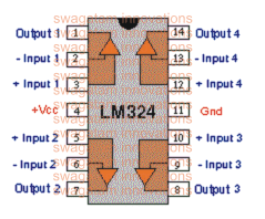
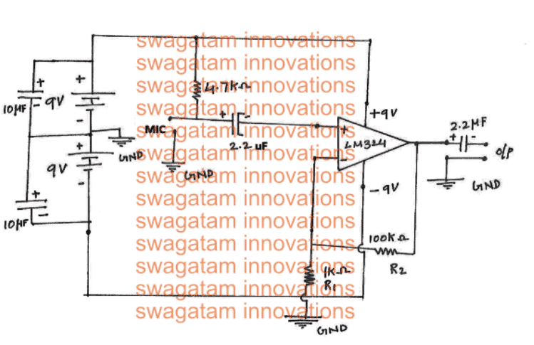 The power source is differential power supply, which consists of two 9V battery coupled with capacitors for smooth and noise less power.
2.2uF capacitor is for eliminating DC voltage entering the IC.
4.7K resistor helps powering the microphone.
R1 and R2 is gain adjust resistor, you may calculate your own values.
2.2uf capacitor at the output is to truncate DC components.
The power source is differential power supply, which consists of two 9V battery coupled with capacitors for smooth and noise less power.
2.2uF capacitor is for eliminating DC voltage entering the IC.
4.7K resistor helps powering the microphone.
R1 and R2 is gain adjust resistor, you may calculate your own values.
2.2uf capacitor at the output is to truncate DC components.
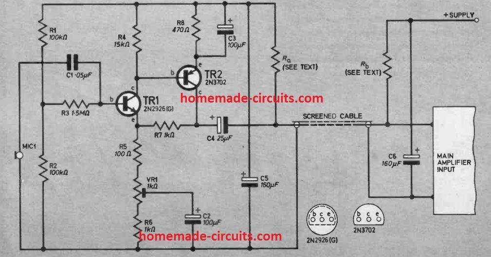 PREAMP SUPPLY
The following figure shows the basic operational details of the design.
PREAMP SUPPLY
The following figure shows the basic operational details of the design.
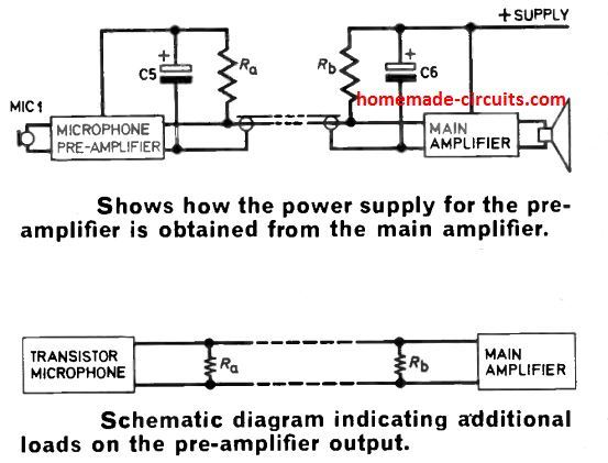 Let's first imagine the supply to the preamplifier coming from the main power amplifier unit.
Resistors Ra and Rb establish the voltage delivered to the preamplifier.
Consequently, when the pre-amplifier draws a I amp current, the voltage getting at the preamplifier can be calculated by
V preamp = Vs - I(Ra + Rb)
where V is the supply voltage.
The pre-amplifier detailed in this article was created to run using at 10V supply.
The current necessary is 2mA.
If we consider the voltage tapping on the main amplifier is Vs and if Ra is made equal to Rb, the above equation simplifies to
Ra = Rb = 250(Vs - 10) ohms
It may be important to note at this stage that this specific approach of acquiring the supply voltage from the main amplifier must be applied only with low voltage transistor amplifiers having a highest voltage tapping of 50V.
The prototype had been intended for amplifiers working with a 20V supply.
Any similar transistor amplifier having this type of supply can be employed.
Thefeore considering the amplifier supply is 20V then
Ra = Rb = 2.5K or simply 2.2K, even this value is not so critical, but not lower than this.
Let's first imagine the supply to the preamplifier coming from the main power amplifier unit.
Resistors Ra and Rb establish the voltage delivered to the preamplifier.
Consequently, when the pre-amplifier draws a I amp current, the voltage getting at the preamplifier can be calculated by
V preamp = Vs - I(Ra + Rb)
where V is the supply voltage.
The pre-amplifier detailed in this article was created to run using at 10V supply.
The current necessary is 2mA.
If we consider the voltage tapping on the main amplifier is Vs and if Ra is made equal to Rb, the above equation simplifies to
Ra = Rb = 250(Vs - 10) ohms
It may be important to note at this stage that this specific approach of acquiring the supply voltage from the main amplifier must be applied only with low voltage transistor amplifiers having a highest voltage tapping of 50V.
The prototype had been intended for amplifiers working with a 20V supply.
Any similar transistor amplifier having this type of supply can be employed.
Thefeore considering the amplifier supply is 20V then
Ra = Rb = 2.5K or simply 2.2K, even this value is not so critical, but not lower than this.
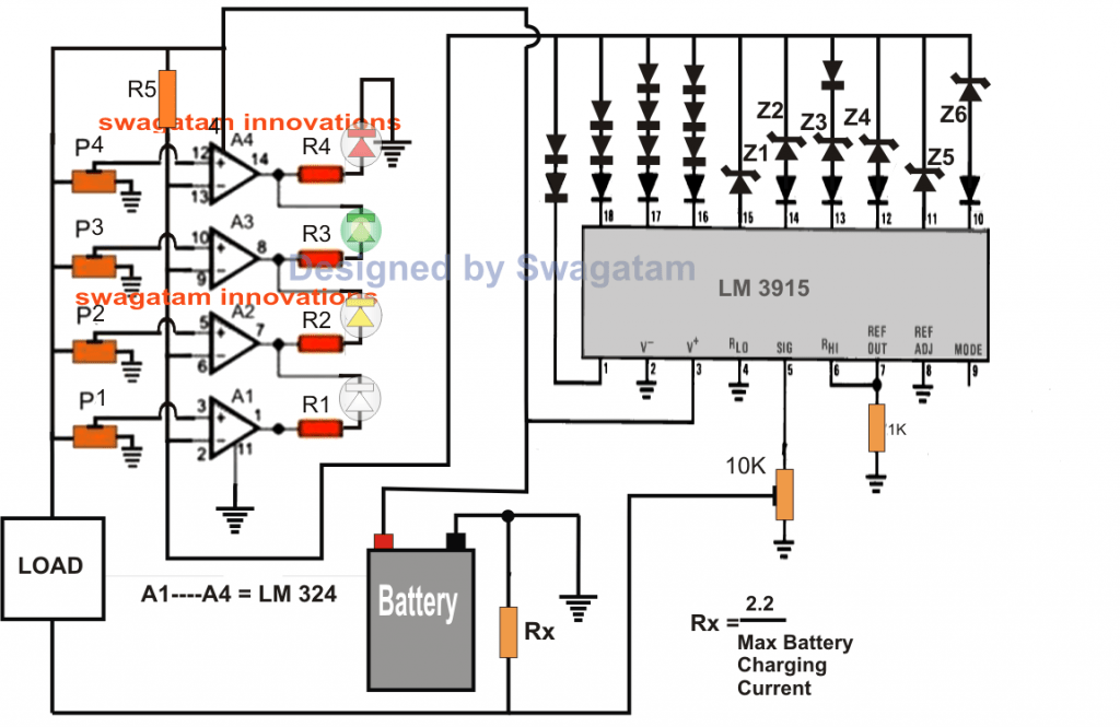
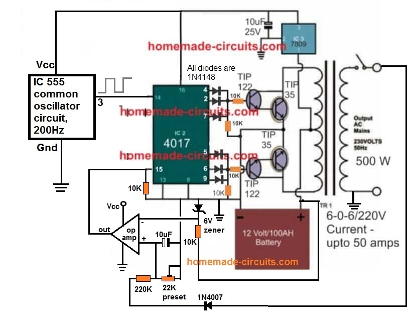 Only the IC 4017 along with its associated diodes, transistors and the transformer will need to be repeated for the required number of inverters.
The oscillator will be a single piece and can be shared with all the inverters by integrating its pin3 with pin14 of the IC 4017.
The feedback circuit must be adjusted precisely for the individual inverters, so that the cut off range is exactly matched for all the inverters.
The following designs and the explanations can be ignored since a much easier version is already updated above
Only the IC 4017 along with its associated diodes, transistors and the transformer will need to be repeated for the required number of inverters.
The oscillator will be a single piece and can be shared with all the inverters by integrating its pin3 with pin14 of the IC 4017.
The feedback circuit must be adjusted precisely for the individual inverters, so that the cut off range is exactly matched for all the inverters.
The following designs and the explanations can be ignored since a much easier version is already updated above
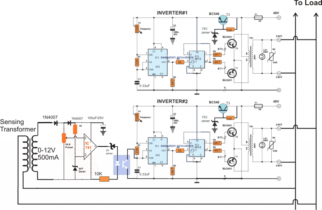 In the figure above we can see a couple of identical stages, where the upper inverter#1 forms the master inverter while the lower inverter#2 the slave.
More stages in the form of inverter#3 and inverter#4 is supposed to be added to the set up in the same identical fashion by integrating these inverters with their indivudual optocoupler stages, but the opamp stage need not be repeated.
The design primarily consists of an IC 555 based oscillator and an IC 4013 flip flop circuit.
The IC 555 is rigged to generate clock frequencies at the rate of 100Hz or 120Hz which is fed to the clock input of the IC 4013, which then converts it into the required 50Hz or 60Hz by alternately flipping its outputs with logic high across pin#1 and pin#2.
These alternating outputs are then used for activating the power devices and the transformer for generating the intended 220V or the 120V AC.
Now as discussed earlier the crucial issue here is to synchronize the two inverters so that these are able to run exactly in sync, with regards to frequency, phase and PWM.
Initially all the involved modules (stackable inverter circuits) are separately adjusted with precisely identical components so that their behavior are perfectly on par with each other.
However even with the precisely matched attributes, the inverters cannot be expected to run perfectly in sync unless these are tied up in some unique manner.
This is in fact done by integrating the the "slave" inverters through an opamp/optocoupler stage as indicated in the above design.
Initially, the master inverter#1 is switched ON, which allows the opamp 741 stage to get powered and to initialize the frequency and phase tracking of the output voltage.
Once this is initiated, the subsequent inverters are all switched ON for adding power to the mains line.
As can be seen the opamp output is connected with the timing capacitor of all the slave inverters through an opto coupler which force the slave inverters to follow the frequency and the phase angle of the master inverter.
However the interesting thing here is the latching factor of the opamp with the instantaneous phase and frequency information.
This happens since all the inverters are now delivering and running at the specified frequency and phase from the master inverter, which implies if in case any of the inverters fail including the master inverter, the opamp is able to quickly track and inject the instantaneous frequency/phase info and force the existing inverters to run with this specifications, and the inverter in turn are able to sustain the feedbacks to the opamp stage to make the transitions seamless and self optimizing.
Therefore hopefully the opamp stage takes care of the first challenge of keeping all the proposed stackable inverters perfectly synchronized through a LIVE tracking of the available mains specification.
In the next part of the article we'll learn the synchronized PWM sinewave stage, which is the next crucial feature of the above discussed design.
In the above part of this article we learned the main section of the 4kva synchronized stackable inverter circuit which explained the synchronization details of the design.
In this article we study how to make the design a sinewave equivalent and also ensure correct synchronization of the PWMs across the involved inverters.
In the figure above we can see a couple of identical stages, where the upper inverter#1 forms the master inverter while the lower inverter#2 the slave.
More stages in the form of inverter#3 and inverter#4 is supposed to be added to the set up in the same identical fashion by integrating these inverters with their indivudual optocoupler stages, but the opamp stage need not be repeated.
The design primarily consists of an IC 555 based oscillator and an IC 4013 flip flop circuit.
The IC 555 is rigged to generate clock frequencies at the rate of 100Hz or 120Hz which is fed to the clock input of the IC 4013, which then converts it into the required 50Hz or 60Hz by alternately flipping its outputs with logic high across pin#1 and pin#2.
These alternating outputs are then used for activating the power devices and the transformer for generating the intended 220V or the 120V AC.
Now as discussed earlier the crucial issue here is to synchronize the two inverters so that these are able to run exactly in sync, with regards to frequency, phase and PWM.
Initially all the involved modules (stackable inverter circuits) are separately adjusted with precisely identical components so that their behavior are perfectly on par with each other.
However even with the precisely matched attributes, the inverters cannot be expected to run perfectly in sync unless these are tied up in some unique manner.
This is in fact done by integrating the the "slave" inverters through an opamp/optocoupler stage as indicated in the above design.
Initially, the master inverter#1 is switched ON, which allows the opamp 741 stage to get powered and to initialize the frequency and phase tracking of the output voltage.
Once this is initiated, the subsequent inverters are all switched ON for adding power to the mains line.
As can be seen the opamp output is connected with the timing capacitor of all the slave inverters through an opto coupler which force the slave inverters to follow the frequency and the phase angle of the master inverter.
However the interesting thing here is the latching factor of the opamp with the instantaneous phase and frequency information.
This happens since all the inverters are now delivering and running at the specified frequency and phase from the master inverter, which implies if in case any of the inverters fail including the master inverter, the opamp is able to quickly track and inject the instantaneous frequency/phase info and force the existing inverters to run with this specifications, and the inverter in turn are able to sustain the feedbacks to the opamp stage to make the transitions seamless and self optimizing.
Therefore hopefully the opamp stage takes care of the first challenge of keeping all the proposed stackable inverters perfectly synchronized through a LIVE tracking of the available mains specification.
In the next part of the article we'll learn the synchronized PWM sinewave stage, which is the next crucial feature of the above discussed design.
In the above part of this article we learned the main section of the 4kva synchronized stackable inverter circuit which explained the synchronization details of the design.
In this article we study how to make the design a sinewave equivalent and also ensure correct synchronization of the PWMs across the involved inverters.
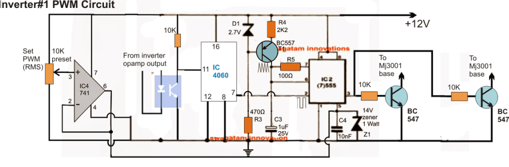 The different stages involved in the above PWM geneartor circuit can be understood with the help of the following point:
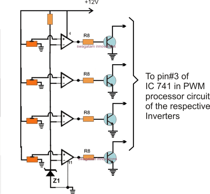 In the figure above we can see four opamps from the IC LM324 configured as four separate comparators with their non-inverting inputs rigged with individual presets,while their inverting inputs all referenced with a fixed zener voltage.
The relevant presets are simply adjusted such that the opamps produce high outputs in a sequential a soon as the mains voltage goes above the intended threshold.....
and vice versa.
When this happens the relevant transistors switch in accordance with the opamp activation.
The collectors of the respective BJTs are connected with the pin#3 of the voltage follower opamp IC 741 which is employed in the PWM controller stage, and this forces the opamp output to go low or zero, which in turn causes a zero voltage to appear at pin#5 of the PWM IC 555 (as discussed in Part 2).
With pin#5 of the IC 555 is applied with this zero logic, forces the PWMs to become narrowest or at the minimum value, which causes the output of that particular inverter to almost shut down.
The above actions make an attempt to stabilize the output to an earlier normal condition which again forces the PWM to get wider and this tug-of-war or a constant switching of the opamps cintinues consistently keeping the output as stable as possible, in response to the variations of the attached loads.
With this automatic load correction implemented within the proposed 4kva stackable inverter circuit almost makes the design complete with all the features requested by the user in Part 1 of the article.
In the figure above we can see four opamps from the IC LM324 configured as four separate comparators with their non-inverting inputs rigged with individual presets,while their inverting inputs all referenced with a fixed zener voltage.
The relevant presets are simply adjusted such that the opamps produce high outputs in a sequential a soon as the mains voltage goes above the intended threshold.....
and vice versa.
When this happens the relevant transistors switch in accordance with the opamp activation.
The collectors of the respective BJTs are connected with the pin#3 of the voltage follower opamp IC 741 which is employed in the PWM controller stage, and this forces the opamp output to go low or zero, which in turn causes a zero voltage to appear at pin#5 of the PWM IC 555 (as discussed in Part 2).
With pin#5 of the IC 555 is applied with this zero logic, forces the PWMs to become narrowest or at the minimum value, which causes the output of that particular inverter to almost shut down.
The above actions make an attempt to stabilize the output to an earlier normal condition which again forces the PWM to get wider and this tug-of-war or a constant switching of the opamps cintinues consistently keeping the output as stable as possible, in response to the variations of the attached loads.
With this automatic load correction implemented within the proposed 4kva stackable inverter circuit almost makes the design complete with all the features requested by the user in Part 1 of the article.

 Flex resistor compared with a coin.

 The flex resistor has limitless applications if you know how to use them.
Here is a simple op-amp circuit paired with a flex resistor.
You can set threshold to trigger the output, if you use an op-amp in comparator mode.
The suggested op-amps are LM324 and LM358; you may also give a try for 741.
You can also pair it with arduino, by giving the flex resistor to analogue read pin of arduino with pull down resistor.
No additional libraries are required.
The flex resistor has limitless applications if you know how to use them.
Here is a simple op-amp circuit paired with a flex resistor.
You can set threshold to trigger the output, if you use an op-amp in comparator mode.
The suggested op-amps are LM324 and LM358; you may also give a try for 741.
You can also pair it with arduino, by giving the flex resistor to analogue read pin of arduino with pull down resistor.
No additional libraries are required.

 Here is an illustration of simple angle sensing for flex resistor.
If the flex resistor is flat, blue LED illuminates, if the resistor is flexed to an angle x (say) green LED illuminates, if it flexes greater than x then, red LED illuminates.
Flex resistors can be also seen in applications which demand simulation of complex movements and patterns, for example it's used for studying precise human finger movements, where the motion of the finger is tracked by flex resistor, decoded and displayed on a screen.
This principle may be adapted by game developers to develop motion based game.
Here is an illustration of simple angle sensing for flex resistor.
If the flex resistor is flat, blue LED illuminates, if the resistor is flexed to an angle x (say) green LED illuminates, if it flexes greater than x then, red LED illuminates.
Flex resistors can be also seen in applications which demand simulation of complex movements and patterns, for example it's used for studying precise human finger movements, where the motion of the finger is tracked by flex resistor, decoded and displayed on a screen.
This principle may be adapted by game developers to develop motion based game.
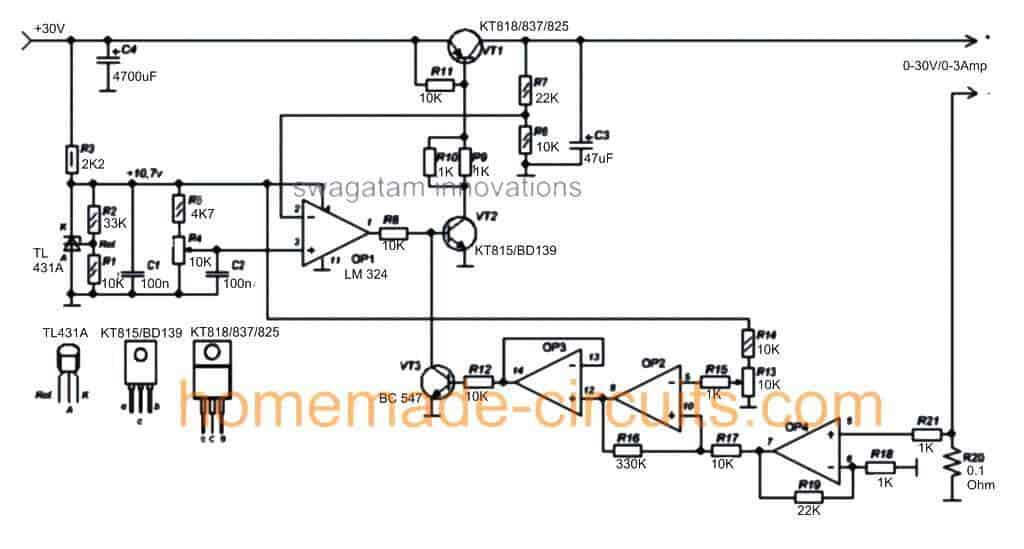 I accidentally found this design from an online website and found it quite interesting, although I already have a similar design published in this site by the name zero drop solar charger circuit, the above shown circuit looks more meticulously designed and therefore is more accurate.
Referring to the above proposed universal power supply circuit diagram, the functional details can be understood with the help of the flowing points:
I accidentally found this design from an online website and found it quite interesting, although I already have a similar design published in this site by the name zero drop solar charger circuit, the above shown circuit looks more meticulously designed and therefore is more accurate.
Referring to the above proposed universal power supply circuit diagram, the functional details can be understood with the help of the flowing points:
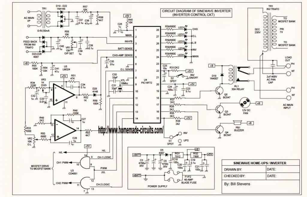
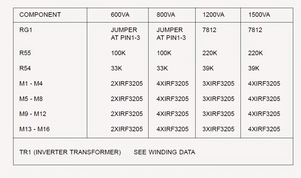 The following data supplies the full transformer winding details:
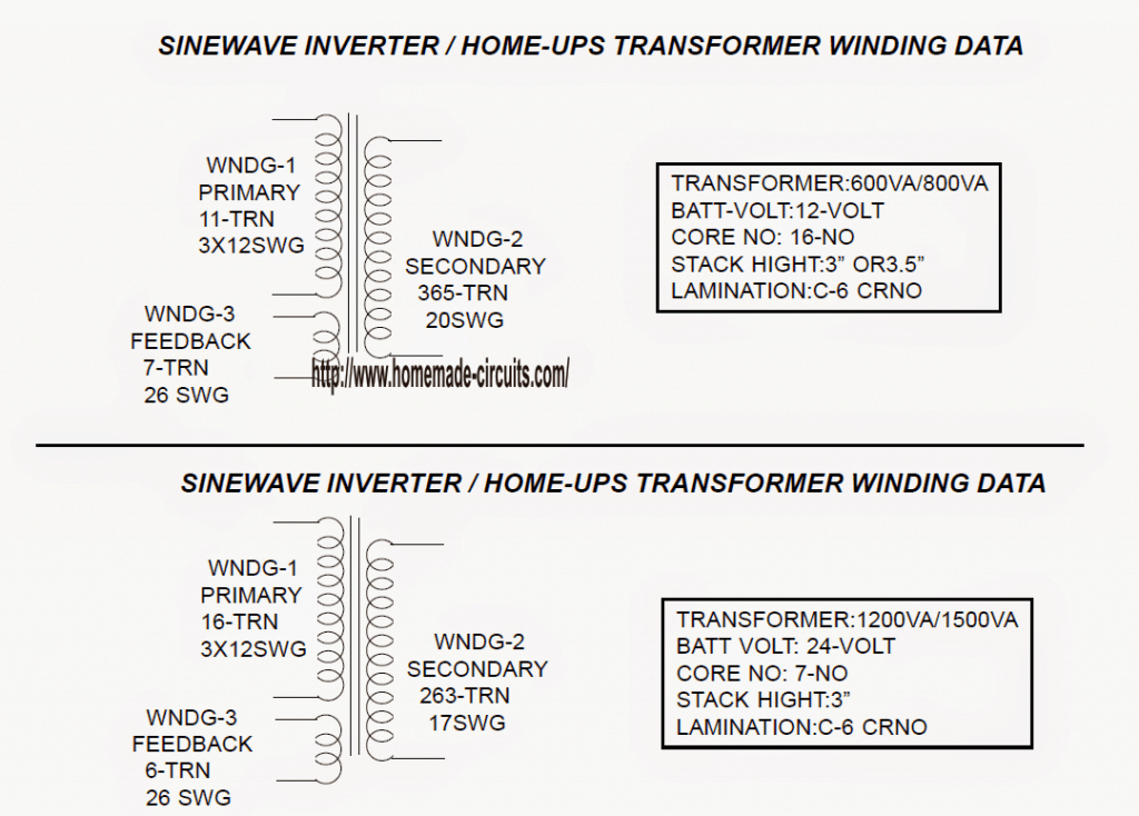 Feedback from Mr.
Hisham:
Hi mr swagatam ,how are you?
I want to tell you that pure sine wave inverter schematic have some mistakes, 220uf bootstrap capacitor should be replaced with a (22uf or 47uf or 68uf),,,a 22uf capacitors which is connected between pin 1 and pin2 of the 2's ir2110 is wrong and should be removed, also a hex code called eletech.
Hex should not be use cause its make inverter shutdown after 15 seconds with low battery led and buzer beeps, if you have big dc fan so the transistors should be replaced with a higher current,for mosfets safety a 7812 regulator is recommended to be connected to ir2110...also there's d14,d15 and d16 should not be connected to ground.
I have tested this inverter and its really pure sine wave,i have run a washing machine and its running silently without any noise, i have connected a 220nf capcitor in the ouput instead of 2.5uf, refrigerator is working too, i will share some pictures soon.
Best regards
Feedback from Mr.
Hisham:
Hi mr swagatam ,how are you?
I want to tell you that pure sine wave inverter schematic have some mistakes, 220uf bootstrap capacitor should be replaced with a (22uf or 47uf or 68uf),,,a 22uf capacitors which is connected between pin 1 and pin2 of the 2's ir2110 is wrong and should be removed, also a hex code called eletech.
Hex should not be use cause its make inverter shutdown after 15 seconds with low battery led and buzer beeps, if you have big dc fan so the transistors should be replaced with a higher current,for mosfets safety a 7812 regulator is recommended to be connected to ir2110...also there's d14,d15 and d16 should not be connected to ground.
I have tested this inverter and its really pure sine wave,i have run a washing machine and its running silently without any noise, i have connected a 220nf capcitor in the ouput instead of 2.5uf, refrigerator is working too, i will share some pictures soon.
Best regards
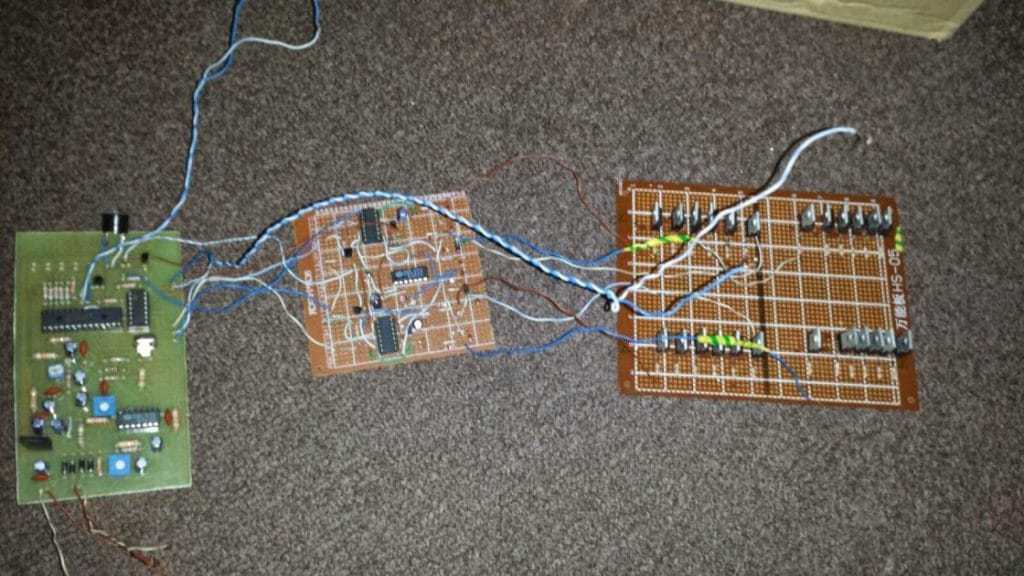
 The schematic discussed in the above article was tested and modified with a few appropriate corrections by Mr.
Hisham, as shown in the following images, viewers can refer to these for improving the performance of the same:
The schematic discussed in the above article was tested and modified with a few appropriate corrections by Mr.
Hisham, as shown in the following images, viewers can refer to these for improving the performance of the same:
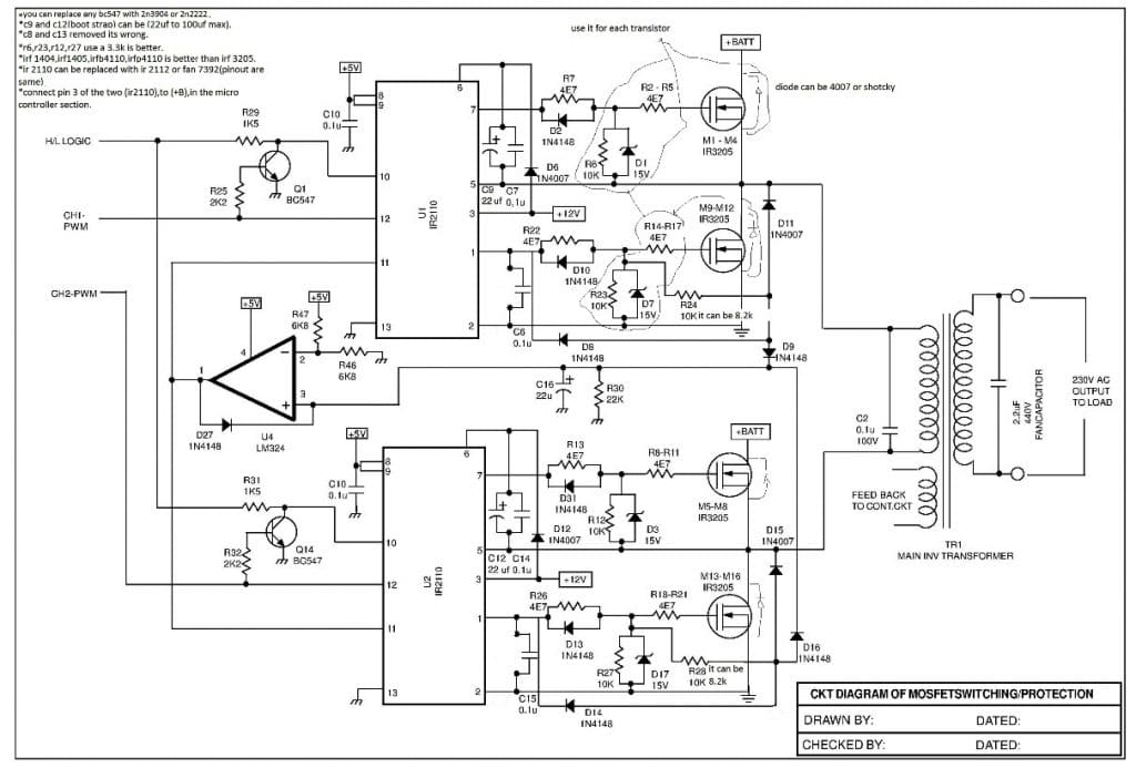
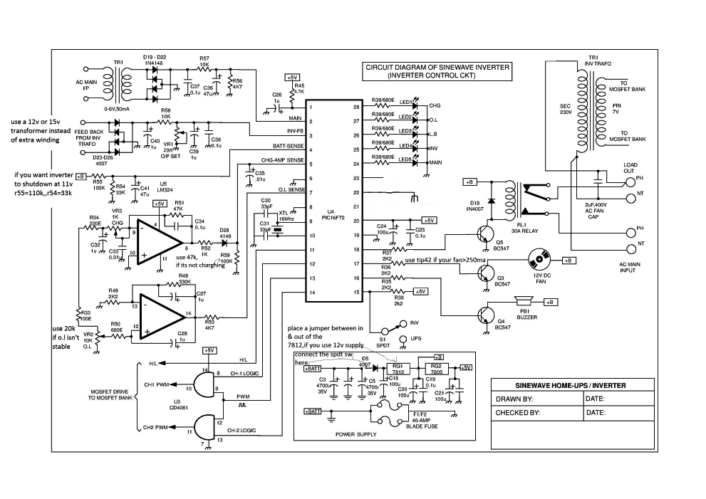 Now let us study how the mosfet switching stage can be built through the following explanation.
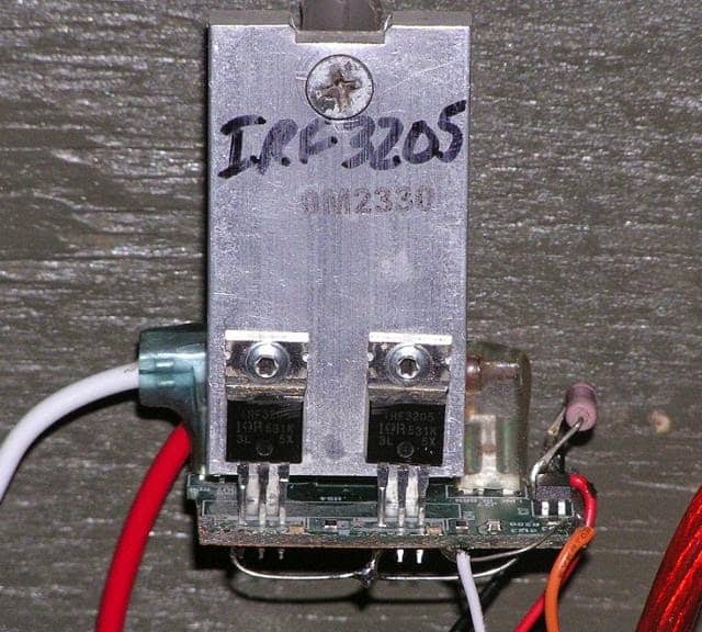
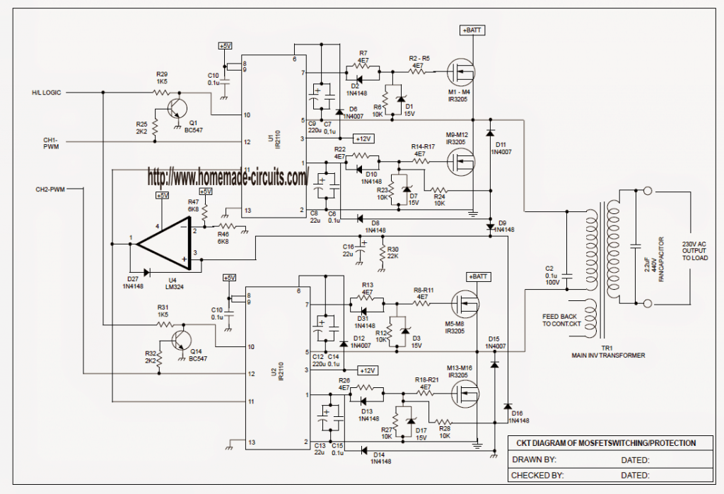 In this case U1 (IR2110) and U2 (IR2110) high side / low side mosfet driver are employed, check with data sheet of this IC to understand more.
In this the two MOSFET banks with high side and low side MOSFETs are intended for transformer��s primary side switching.
In this case we are discussing the functioning of bank (applying IC U1) only since the supplementary bank driving does not differ from from each other.
As soon as the inverter is ON the controller renders the pin10 of U1 is logic high which subsequently activates the high side MOSFETs (M1 - M4) ON, PWM for channel-1 from pin10 of CD4081 is applied to pin12 of the drver IC (U1) and likewise it is administered to the base of Q1 via R25.
While the PWM is logic high the pin12 of U1 is also logic high and triggers the low side MOSFETs of bank 1(M9 - M12), alternately it launches the transistor
Q1 which correspondingly renders the pin10 voltage of U1 logic low, thereupon turning OFF the high side MOSFETs (M1 - M4).
Therefore it implies that by default the high logic from pin11 of the microcontroller gets switched ON for the high side MOSFETs among the two the mosfet arrays, and while the associated PWM is high the low side MOSFETs are turned ON and the high side MOSFETs are switched OFF, and through this way the switching sequence keeps repeating.
In this case U1 (IR2110) and U2 (IR2110) high side / low side mosfet driver are employed, check with data sheet of this IC to understand more.
In this the two MOSFET banks with high side and low side MOSFETs are intended for transformer��s primary side switching.
In this case we are discussing the functioning of bank (applying IC U1) only since the supplementary bank driving does not differ from from each other.
As soon as the inverter is ON the controller renders the pin10 of U1 is logic high which subsequently activates the high side MOSFETs (M1 - M4) ON, PWM for channel-1 from pin10 of CD4081 is applied to pin12 of the drver IC (U1) and likewise it is administered to the base of Q1 via R25.
While the PWM is logic high the pin12 of U1 is also logic high and triggers the low side MOSFETs of bank 1(M9 - M12), alternately it launches the transistor
Q1 which correspondingly renders the pin10 voltage of U1 logic low, thereupon turning OFF the high side MOSFETs (M1 - M4).
Therefore it implies that by default the high logic from pin11 of the microcontroller gets switched ON for the high side MOSFETs among the two the mosfet arrays, and while the associated PWM is high the low side MOSFETs are turned ON and the high side MOSFETs are switched OFF, and through this way the switching sequence keeps repeating.
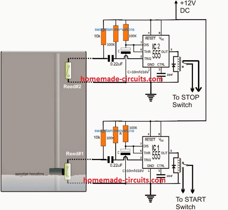 The diagram above shows a very straightforward set up using a couple of identical IC 555 monostable stages.
The IC2 stage forms the submersible pump starter circuit, while the IC2 stage is positioned to stop the pump switch.
Both the circuits work with reed switches (float switch) which may be seen positioned inside the overhead tank, one at the bottom, the other at the top of the tank.
The bottom reed closes when the water level is near the bottom threshold, and parallel to the reed switch, while the upper reed switch closes when the water level reaches at the level where its been installed.
Assuming the water level to be near the bottom reed switch, the reed switch closes, triggering the IC1 stage, which in turn momentarily clicks the associated relay.
The relay being wired across the START button of the submersible pump, the motor gets initiated and it starts pumping water to the overhead tank.
The water level in the OHT now begins rising, and when it reaches near the upper reed switch reed#2, it closes triggering the IC2 relay for a moment activating the STOP switch of the motor.
The motor now stops and discontinues the pumping of water inside the OHT.
The diagram above shows a very straightforward set up using a couple of identical IC 555 monostable stages.
The IC2 stage forms the submersible pump starter circuit, while the IC2 stage is positioned to stop the pump switch.
Both the circuits work with reed switches (float switch) which may be seen positioned inside the overhead tank, one at the bottom, the other at the top of the tank.
The bottom reed closes when the water level is near the bottom threshold, and parallel to the reed switch, while the upper reed switch closes when the water level reaches at the level where its been installed.
Assuming the water level to be near the bottom reed switch, the reed switch closes, triggering the IC1 stage, which in turn momentarily clicks the associated relay.
The relay being wired across the START button of the submersible pump, the motor gets initiated and it starts pumping water to the overhead tank.
The water level in the OHT now begins rising, and when it reaches near the upper reed switch reed#2, it closes triggering the IC2 relay for a moment activating the STOP switch of the motor.
The motor now stops and discontinues the pumping of water inside the OHT.
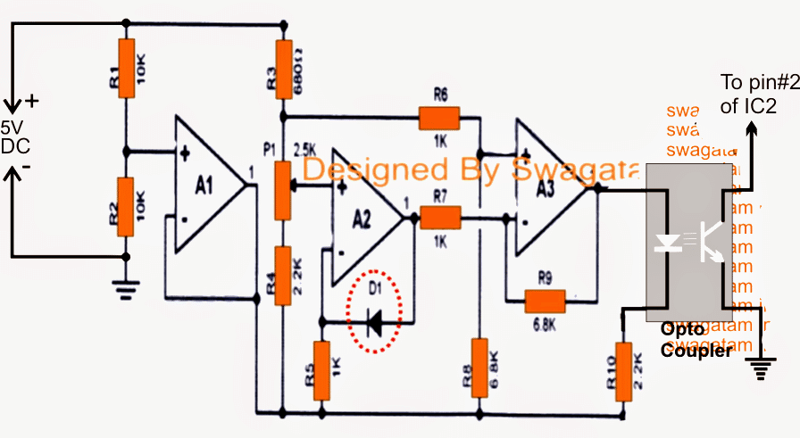
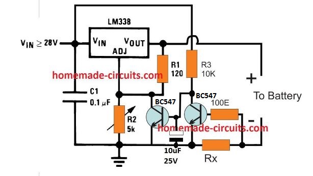 I forgot to add a diode at the battery positive line, so please make sure to add it as shown in the following corrected diagram.
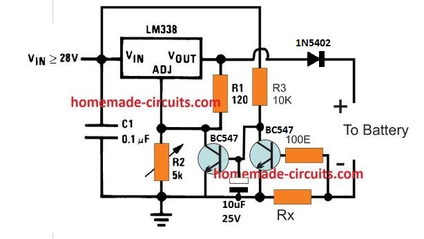
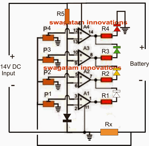
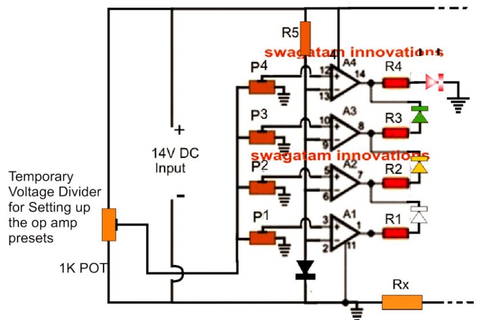 Initially, disconnect the P1---P4 preset link from the Rx and connect it with the center pin of the 1 K pot, as indicated above.
Slide the center arm of all the op amp presets towards the 1K pot.
Now, adjust the 1K pot so that 2.5V is developed across its center arm and the ground arm.
You will find only the RED LED is ON at this point.
Next, adjust the A4 preset P4 so that the RED LED just shuts off.
This will instantly switch ON A3 Green LED.
After this adjust the 1K pot to reduce its center pin voltage to 2V.
As above, adjust the A3 preset P3 so that the Green just shuts OFF.
This will switch ON the yellow LED.
Next, adjust the 1K pot to produce 1.5V at its center pin, and adjust the A2 preset P2 so that the Yellow LED just shuts off.
This will switch ON the white LED.
Finally, adjust the 1K pot to reduce its center pin potential to 0.5V.
Adjust the A1 preset P1 such that the white LED just shuts off.
The preset adjustments is now over and done!
Remove the 1K pot and reconnect the preset output link back to Rx as show in the first diagram.
You can can start charging the recommended battery and watch the LEDs respond accordingly.
Initially, disconnect the P1---P4 preset link from the Rx and connect it with the center pin of the 1 K pot, as indicated above.
Slide the center arm of all the op amp presets towards the 1K pot.
Now, adjust the 1K pot so that 2.5V is developed across its center arm and the ground arm.
You will find only the RED LED is ON at this point.
Next, adjust the A4 preset P4 so that the RED LED just shuts off.
This will instantly switch ON A3 Green LED.
After this adjust the 1K pot to reduce its center pin voltage to 2V.
As above, adjust the A3 preset P3 so that the Green just shuts OFF.
This will switch ON the yellow LED.
Next, adjust the 1K pot to produce 1.5V at its center pin, and adjust the A2 preset P2 so that the Yellow LED just shuts off.
This will switch ON the white LED.
Finally, adjust the 1K pot to reduce its center pin potential to 0.5V.
Adjust the A1 preset P1 such that the white LED just shuts off.
The preset adjustments is now over and done!
Remove the 1K pot and reconnect the preset output link back to Rx as show in the first diagram.
You can can start charging the recommended battery and watch the LEDs respond accordingly.
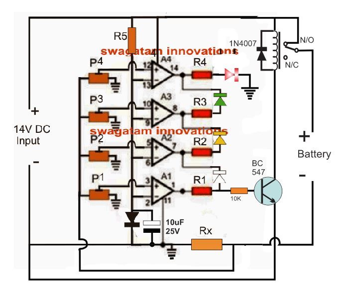
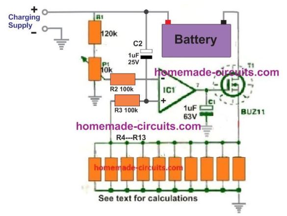 The working of this design is actually simple.
The voltage at the inverting input is fixed by the P1 preset at a level that is just lower than the voltage drop across the resistor bank R3---R13, corresponding to the recommended charging current of the battery.
When power is switched ON, C2 causes a high to appear at the non-inverting of the op amp which in turn causes the op amp output to go high and switch ON the MOSFET.
The MOSFET conducts and allows the battery to be connected across the charging supply, enabling the charging current to pass through the resistor bank.
This allows a voltage to develop at the non-inverting input of the IC, higher than its inverting pin, which latches the output of the op amp to a permanent high.
The MOSFET now continues to conduct and the battery is charged, until the current intake of the battery decreases significantly at the full charge level of the battery.
The voltage across the resistor bank now drops, so that the inverting pin of the op amp now goes higher than the non-inverting pin of the op amp.
Due to this, the op amp output turns low, the MOSFET is switched OFF, and the battery charging is finally halted.
The working of this design is actually simple.
The voltage at the inverting input is fixed by the P1 preset at a level that is just lower than the voltage drop across the resistor bank R3---R13, corresponding to the recommended charging current of the battery.
When power is switched ON, C2 causes a high to appear at the non-inverting of the op amp which in turn causes the op amp output to go high and switch ON the MOSFET.
The MOSFET conducts and allows the battery to be connected across the charging supply, enabling the charging current to pass through the resistor bank.
This allows a voltage to develop at the non-inverting input of the IC, higher than its inverting pin, which latches the output of the op amp to a permanent high.
The MOSFET now continues to conduct and the battery is charged, until the current intake of the battery decreases significantly at the full charge level of the battery.
The voltage across the resistor bank now drops, so that the inverting pin of the op amp now goes higher than the non-inverting pin of the op amp.
Due to this, the op amp output turns low, the MOSFET is switched OFF, and the battery charging is finally halted.
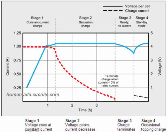 Stage#1: At the initial stage#1 we see that the battery voltage rises from 0.25 V to 4.0 V level in around one hour at 1 amp constant current charging rate.
This is indicated by the BLUE line.
The 0.25 V is only for indicative purpose, an actual 3.7 V cell should never be discharged below 3 V.
Stage#2: In stage#2, the charging enters the saturation charge state, where the voltage peaks to the full charge level of 4.2 V, and the current consumption begins dropping.
This drop in the current rate continues for the next couple of hours.
The charging current is indicated by the RED dotted line.
Stage#3: As the current drops, it reaches its lowest level which is lower than 3% of the cell's Ah rating.
Once this happens, the input supply is switched OFF and the cell is allowed to settle down for another 1 hour.
After one hour the cell voltage indicates the real State-Of-Charge or the SoC of the cell.
The SoC of a cell or battery is the optimal charge level which it has attained after a course of full charging, and this level shows the actual level which can be used for a given application.
At this state we can say the cell condition is ready to use.
Stage#4: In situations where the cell is not used for long periods, a topping up charging is applied from time to time, wherein the current consumed by the cell is below 3% of its Ah value.
Stage#1: At the initial stage#1 we see that the battery voltage rises from 0.25 V to 4.0 V level in around one hour at 1 amp constant current charging rate.
This is indicated by the BLUE line.
The 0.25 V is only for indicative purpose, an actual 3.7 V cell should never be discharged below 3 V.
Stage#2: In stage#2, the charging enters the saturation charge state, where the voltage peaks to the full charge level of 4.2 V, and the current consumption begins dropping.
This drop in the current rate continues for the next couple of hours.
The charging current is indicated by the RED dotted line.
Stage#3: As the current drops, it reaches its lowest level which is lower than 3% of the cell's Ah rating.
Once this happens, the input supply is switched OFF and the cell is allowed to settle down for another 1 hour.
After one hour the cell voltage indicates the real State-Of-Charge or the SoC of the cell.
The SoC of a cell or battery is the optimal charge level which it has attained after a course of full charging, and this level shows the actual level which can be used for a given application.
At this state we can say the cell condition is ready to use.
Stage#4: In situations where the cell is not used for long periods, a topping up charging is applied from time to time, wherein the current consumed by the cell is below 3% of its Ah value.
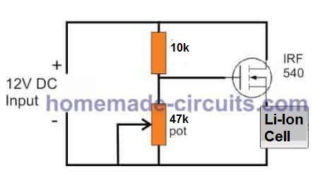 NOTE: This design is without temperature regulation, therefore lower input current is recommended.
A single MOSFET, a preset or trimmer and a 470 ohm 1/4 watt resistor is all that you would need to make a simple and safe charger circuit.
Before connecting the output to a Li-Ion cell make sure of a couple of things.
1) Since the above design does not incorporate temperature regulation, the input current must be restricted to a level which does not cause significant heating of the cell.
2) Adjust the preset to get exactly 4.1V across the charging terminals where the cell is supposed to be connected.
A great way to fix this is to connect a precise zener diode in place of the preset, and replace the 470 ohm with a 1 K resistor.
For the current, typically a constant current input of around 0.5C would be just right, that is 50% of the mAh value of the cell.
Adding a Current Controller
If the input source is not current controlled, in that case we can quickly upgrade the above circuit with a simple BJT current control stage as shown below:
NOTE: This design is without temperature regulation, therefore lower input current is recommended.
A single MOSFET, a preset or trimmer and a 470 ohm 1/4 watt resistor is all that you would need to make a simple and safe charger circuit.
Before connecting the output to a Li-Ion cell make sure of a couple of things.
1) Since the above design does not incorporate temperature regulation, the input current must be restricted to a level which does not cause significant heating of the cell.
2) Adjust the preset to get exactly 4.1V across the charging terminals where the cell is supposed to be connected.
A great way to fix this is to connect a precise zener diode in place of the preset, and replace the 470 ohm with a 1 K resistor.
For the current, typically a constant current input of around 0.5C would be just right, that is 50% of the mAh value of the cell.
Adding a Current Controller
If the input source is not current controlled, in that case we can quickly upgrade the above circuit with a simple BJT current control stage as shown below:
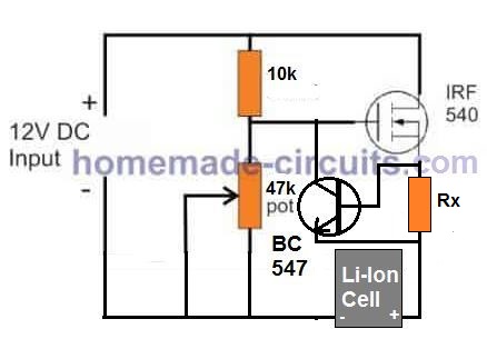 RX = 07 / Max Charging Current
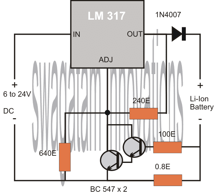 The above circuit works with temperature compensation principle, but it does not incorporate an automatic over charge cut off feature, and therefore the maximum charging voltage is being fixed at 4.1 V.
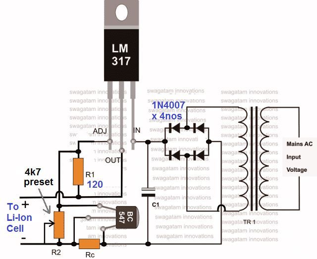 Transformer can be a 0-6/9/12V transformer
Since, here temperature control is not employed, make sure that Rc value is correctly dimensioned for a 0.5 C rate.
For this you can use the following formula:
Rc = 0.7 / 50% of Ah value
Suppose the Ah value is printed as 2800 mAh.
Then the above formula could be solved as:
Rc = 0.7 / 1400 mA = 0.7 / 1.4 = 0.5 Ohms
Wattage will be 0.7 x 1.4 = 0.98, or simply 1 watt.
Likewise, make sure the 4k7 preset is adjusted to an exact 4.1 V across the output terminals.
Once the above adjustments are made, you can charge the intended Li-Ion battery safely, without worrying about any untoward situation.
Since, at 4.1 V we cannot assume the battery to be fully charged.
To counter the above drawback, an automatic cut off facility becomes more favorable than the above concept.
I have discussed many op amp automatic charger circuits in this blog, any one of them can be applied for the proposed design, but since we are interested to keep the design cheap and easy, an alternative idea which is shown below can be tried.
Transformer can be a 0-6/9/12V transformer
Since, here temperature control is not employed, make sure that Rc value is correctly dimensioned for a 0.5 C rate.
For this you can use the following formula:
Rc = 0.7 / 50% of Ah value
Suppose the Ah value is printed as 2800 mAh.
Then the above formula could be solved as:
Rc = 0.7 / 1400 mA = 0.7 / 1.4 = 0.5 Ohms
Wattage will be 0.7 x 1.4 = 0.98, or simply 1 watt.
Likewise, make sure the 4k7 preset is adjusted to an exact 4.1 V across the output terminals.
Once the above adjustments are made, you can charge the intended Li-Ion battery safely, without worrying about any untoward situation.
Since, at 4.1 V we cannot assume the battery to be fully charged.
To counter the above drawback, an automatic cut off facility becomes more favorable than the above concept.
I have discussed many op amp automatic charger circuits in this blog, any one of them can be applied for the proposed design, but since we are interested to keep the design cheap and easy, an alternative idea which is shown below can be tried.
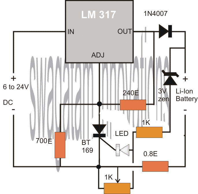
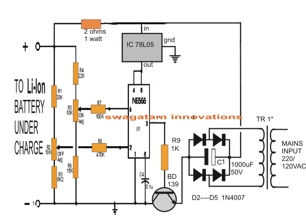 If you feel that the above design is much complex you could try the following design which looks much simpler:
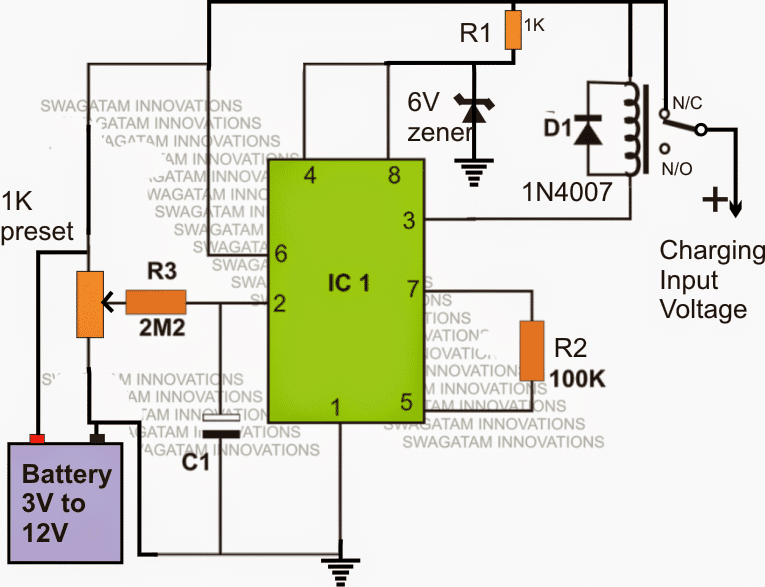
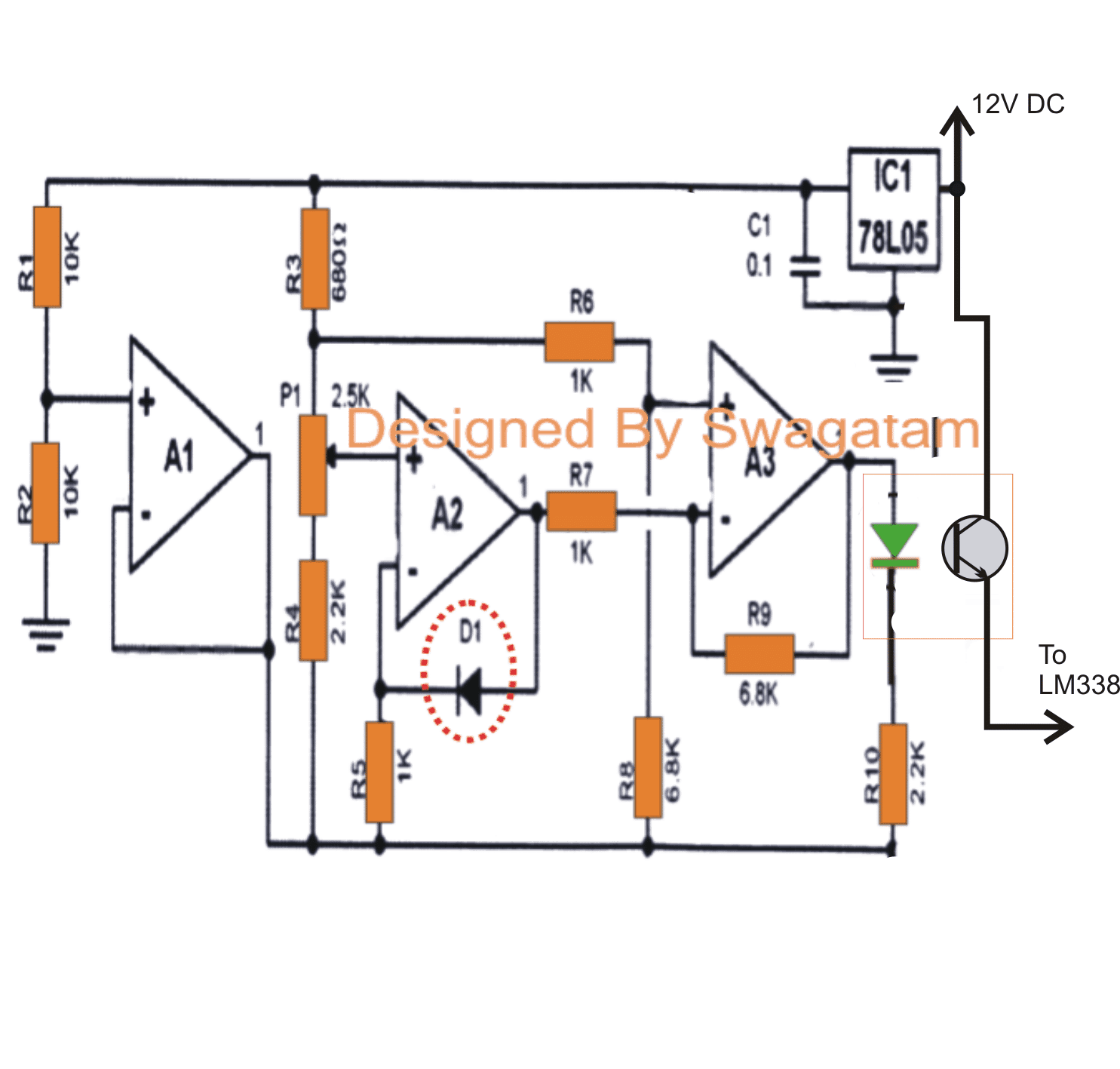 Automatic Li-Ion Cell Charger and Controller Circuit.
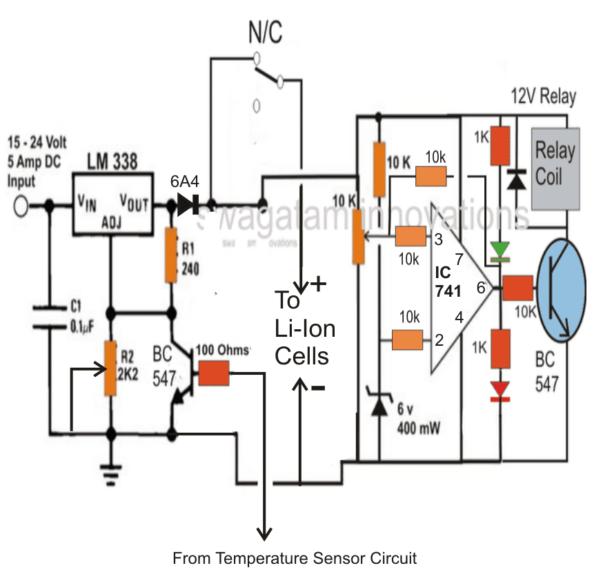 Conclusion
The basic criteria that needs to be maintained for any battery are: charging under convenient temperatures, and cutting off the supply as soon as it reaches the full charge.
That's the basic thing you need to follow regardless of the battery type.
You can monitor this manually or make it automatic, under both cases your battery will charge safely and have a longer life.
The charging/discharging current is responsible for the temperature of the battery, if these are too high compared to the ambient temperature then your battery will suffer heavily in the long run.
Second important factor is never allowing the battery to discharge heavily.
Keep restoring the full charge level or keep topping it up whenever possible.
This will ensure that the battery never reaches its lower discharge levels.
If you find it difficult to monitor this manually then you can go for an automatic circuit as described on this page.
Have further doubts? Please let them come through the comment box below
Conclusion
The basic criteria that needs to be maintained for any battery are: charging under convenient temperatures, and cutting off the supply as soon as it reaches the full charge.
That's the basic thing you need to follow regardless of the battery type.
You can monitor this manually or make it automatic, under both cases your battery will charge safely and have a longer life.
The charging/discharging current is responsible for the temperature of the battery, if these are too high compared to the ambient temperature then your battery will suffer heavily in the long run.
Second important factor is never allowing the battery to discharge heavily.
Keep restoring the full charge level or keep topping it up whenever possible.
This will ensure that the battery never reaches its lower discharge levels.
If you find it difficult to monitor this manually then you can go for an automatic circuit as described on this page.
Have further doubts? Please let them come through the comment box below
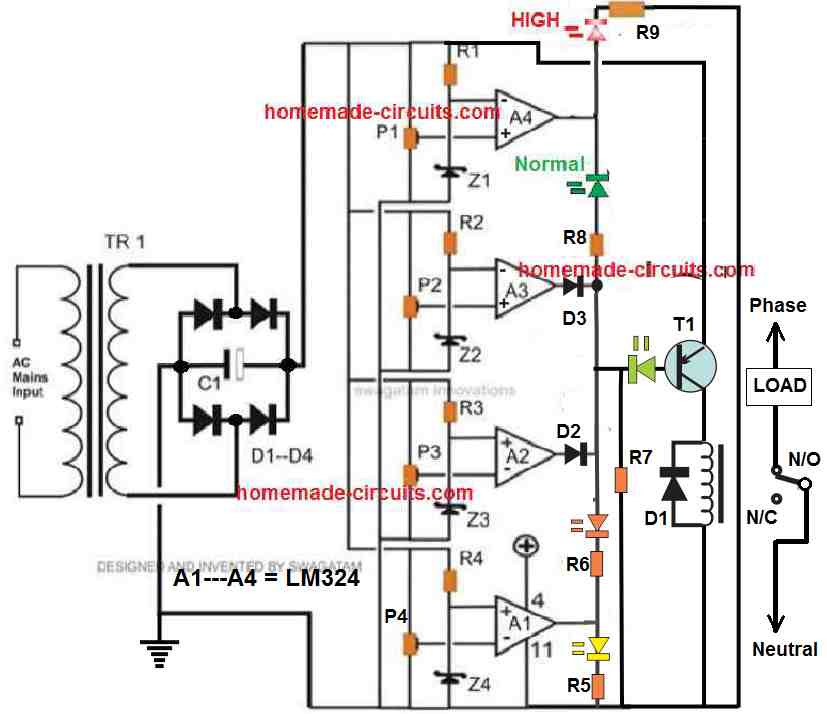 Parts List for the proposed high, low mains voltage protector circuit.
R1, R2, R3, R4, R5, R6, R7, R8, R9 = 4K7,
P1, P2, P3, P4 = 10 K Presets
C1 = 1000 uF/ 25 V,
Z1, Z2, Z3, Z4 = 6 Volts, 400 mW,
D1 = 1N4007,
D2, D3 = 1N4148,
T1 = BC557B,
LED = All are 20 mA, 3.3 V
Transformer = 0 �C 12 V, 500 mA
Relay = SPDT, 12 Volt, 400 Ohm
Parts List for the proposed high, low mains voltage protector circuit.
R1, R2, R3, R4, R5, R6, R7, R8, R9 = 4K7,
P1, P2, P3, P4 = 10 K Presets
C1 = 1000 uF/ 25 V,
Z1, Z2, Z3, Z4 = 6 Volts, 400 mW,
D1 = 1N4007,
D2, D3 = 1N4148,
T1 = BC557B,
LED = All are 20 mA, 3.3 V
Transformer = 0 �C 12 V, 500 mA
Relay = SPDT, 12 Volt, 400 Ohm
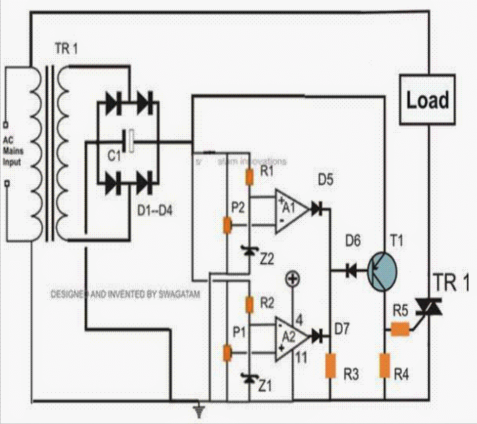 The transformerless mains high low voltage cut off circuit version of the above explained design can be visualized in the following diagram:
Warning: The below shown circuit is not isolated from mains AC.
Handle with extreme caution to avoid a fatal mishap.
The transformerless mains high low voltage cut off circuit version of the above explained design can be visualized in the following diagram:
Warning: The below shown circuit is not isolated from mains AC.
Handle with extreme caution to avoid a fatal mishap.
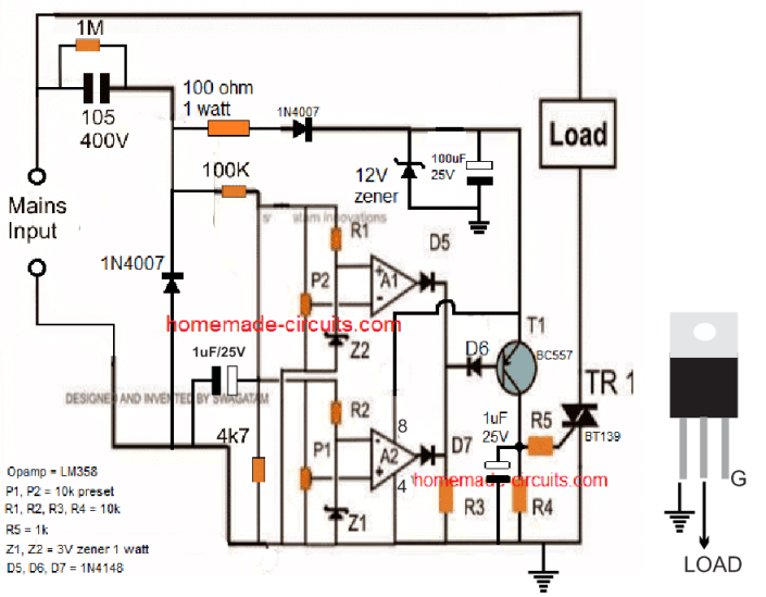
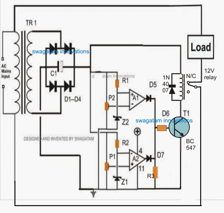 Please use a 22uF/25V capacitor across the transistor base and ground, just to make sure the relay does not stutter during the changeover periods...
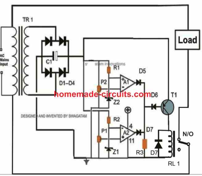
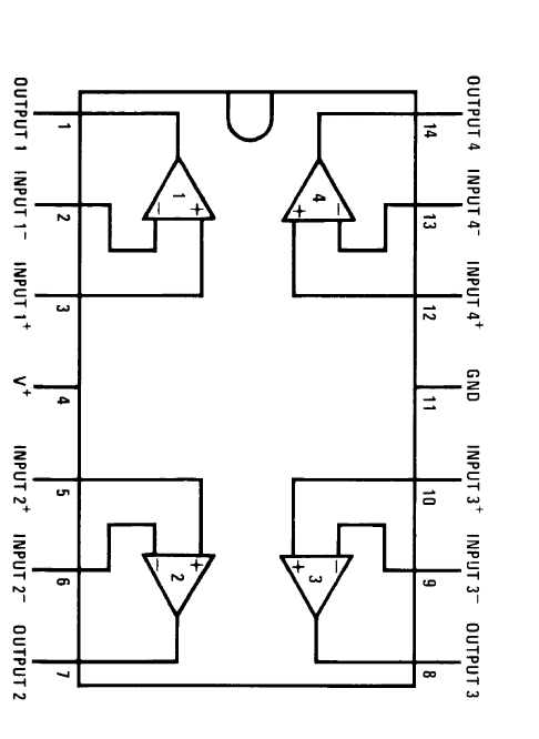
 So far we learned an IC version of the circuit, now let's see how a mains 220V or 120V operated over voltage and under voltage protection circuit can be built using just a couple of transistors.
A very simple circuit presented when installed in the house electrical may help in restricting the issue to a great extent.
Here we will learn two designs of over and under voltage circuits, the first based on transistors and the other one using an opamp.
So far we learned an IC version of the circuit, now let's see how a mains 220V or 120V operated over voltage and under voltage protection circuit can be built using just a couple of transistors.
A very simple circuit presented when installed in the house electrical may help in restricting the issue to a great extent.
Here we will learn two designs of over and under voltage circuits, the first based on transistors and the other one using an opamp.
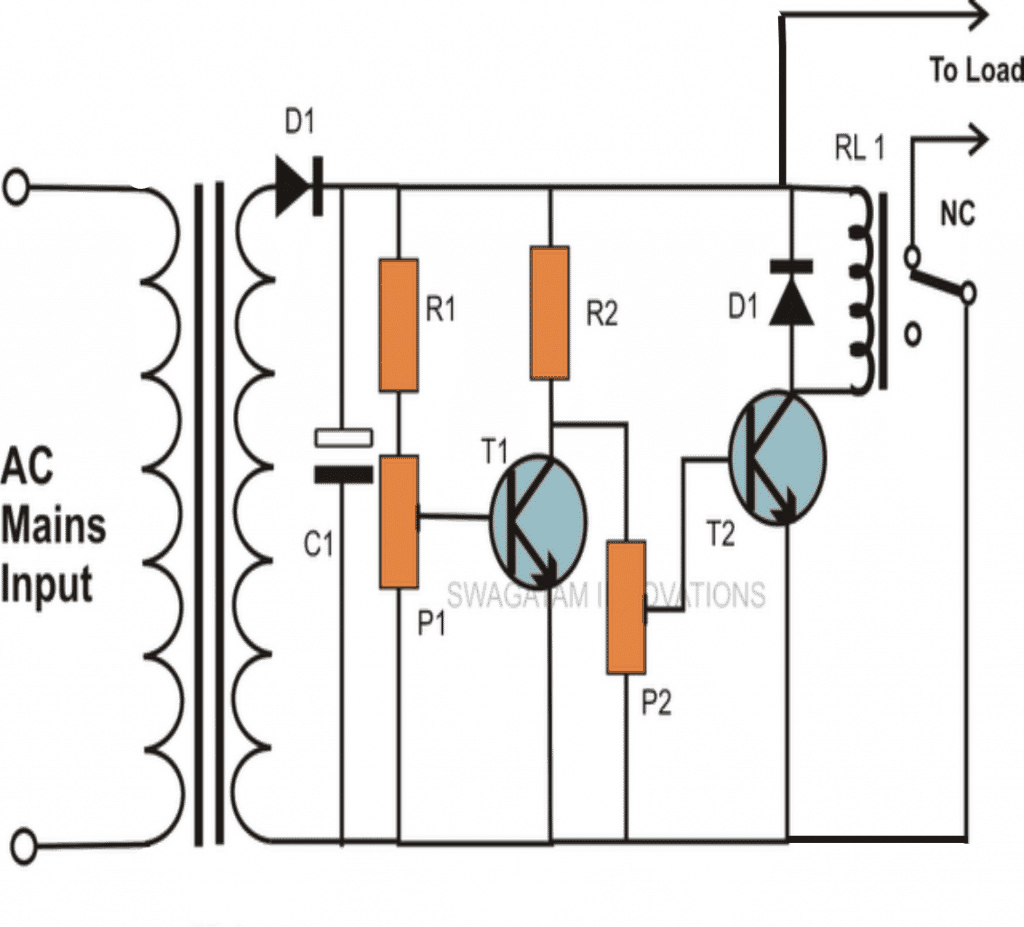 Therefore, the circuit may not be very useful for folks who might be looking for absolutely accurate tripping points and controls which can be optimized as per ones personal preference.
To make this possible a couple of opamps may be required to be included instead of transistors.
Therefore, the circuit may not be very useful for folks who might be looking for absolutely accurate tripping points and controls which can be optimized as per ones personal preference.
To make this possible a couple of opamps may be required to be included instead of transistors.
 The pulses generated by this oscillator are delivered to a decade up-counter chip using the IC 4017, which has its ten output lines turning high sequentially.
These output channels are sent across four encoding and driving transistors which light up the connected LEDs in the specified pattern.
In this LED star circuit, the values of resistors R1, R2, along with C1 could be modified in case you want the Star to light up at some other rate.
Transistors Q1 -Q4 could be any general purpose NPN BJT rated at a 50mA collector capacity.
The complete assembly should not take over two hours.
Overall expense of the design should cost less than $5 and could be possibly reduced for those who have a couple of components from their electronic junk box.
Design of the LED star is not really crucial apart from the placements of the LEDs.
Different modifications from the proposed design might or might not be aesthetically attractive.
If the LED positioning is not done correctly might stop some of the LEDs to light up.
The power supply for the simple LED star circuit can vary from 5 -12 VDC with 6 to 9 V being the most suitable.
A 9 V PP3 cell will allow the circuit to operate for approximately five to six hours, however bigger lead acid batteries should emable the circuit to function for a considerably longer time period, due to the fact that the current consumption of the project is 40 mA at 6 volts.
The pulses generated by this oscillator are delivered to a decade up-counter chip using the IC 4017, which has its ten output lines turning high sequentially.
These output channels are sent across four encoding and driving transistors which light up the connected LEDs in the specified pattern.
In this LED star circuit, the values of resistors R1, R2, along with C1 could be modified in case you want the Star to light up at some other rate.
Transistors Q1 -Q4 could be any general purpose NPN BJT rated at a 50mA collector capacity.
The complete assembly should not take over two hours.
Overall expense of the design should cost less than $5 and could be possibly reduced for those who have a couple of components from their electronic junk box.
Design of the LED star is not really crucial apart from the placements of the LEDs.
Different modifications from the proposed design might or might not be aesthetically attractive.
If the LED positioning is not done correctly might stop some of the LEDs to light up.
The power supply for the simple LED star circuit can vary from 5 -12 VDC with 6 to 9 V being the most suitable.
A 9 V PP3 cell will allow the circuit to operate for approximately five to six hours, however bigger lead acid batteries should emable the circuit to function for a considerably longer time period, due to the fact that the current consumption of the project is 40 mA at 6 volts.

 The block diagram of the school timer using IC 4017 starts from left hand side and ends at right hand side.
The first stage of the block diagram is a 1 Hz generator using IC 555 which provides the clock signal for rest of the circuit.
There are three IC 4017 configured as ��divided by 10�� and one IC 4017 configured as ��divided by 6��.
The first IC 4017 divides the input clock by 10 and outputs one clock cycle for every 10 clock cycle (seconds).
Another IC 4017 is cascaded with the previous IC 4017, which divides the input clock signal by a factor of 6. Now we will get one clock cycle for every minute.
Now an optional stage can be introduced here to count the minutes which will explained in the later part of this post.
The last two IC 4017s are configured as divided by 10 and one of the IC will output the ��units digit�� of the minute and the other IC will output ��tens digit�� of the minute.
The time can be set using the provided two DIP switches for units and tens position of minute digit.
A logic AND gate is utilized to make decision, when the two inputs from IC 4017s are high the Logic gate output turns high and triggers the monostable multivibrator.
The monostable multivibrator��s output turns high for pre-defined period of time which in turns activates the bell until the multivibrator turns low.
Now let��s dive into the circuit diagram of each stage.
The block diagram of the school timer using IC 4017 starts from left hand side and ends at right hand side.
The first stage of the block diagram is a 1 Hz generator using IC 555 which provides the clock signal for rest of the circuit.
There are three IC 4017 configured as ��divided by 10�� and one IC 4017 configured as ��divided by 6��.
The first IC 4017 divides the input clock by 10 and outputs one clock cycle for every 10 clock cycle (seconds).
Another IC 4017 is cascaded with the previous IC 4017, which divides the input clock signal by a factor of 6. Now we will get one clock cycle for every minute.
Now an optional stage can be introduced here to count the minutes which will explained in the later part of this post.
The last two IC 4017s are configured as divided by 10 and one of the IC will output the ��units digit�� of the minute and the other IC will output ��tens digit�� of the minute.
The time can be set using the provided two DIP switches for units and tens position of minute digit.
A logic AND gate is utilized to make decision, when the two inputs from IC 4017s are high the Logic gate output turns high and triggers the monostable multivibrator.
The monostable multivibrator��s output turns high for pre-defined period of time which in turns activates the bell until the multivibrator turns low.
Now let��s dive into the circuit diagram of each stage.
 The above circuit consists of an IC 555 configured as astable multivibrator which generates square wave at pin number three.
It can generate 1 Hz clock signal if you adjust the 100K potentiometer correctly.
The timing accuracy of rest of the circuit depends on how accurately you calibrate this stage.
IC 555 pin diagram:
The above circuit consists of an IC 555 configured as astable multivibrator which generates square wave at pin number three.
It can generate 1 Hz clock signal if you adjust the 100K potentiometer correctly.
The timing accuracy of rest of the circuit depends on how accurately you calibrate this stage.
IC 555 pin diagram:
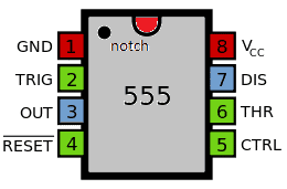 Timer / Counter stage:
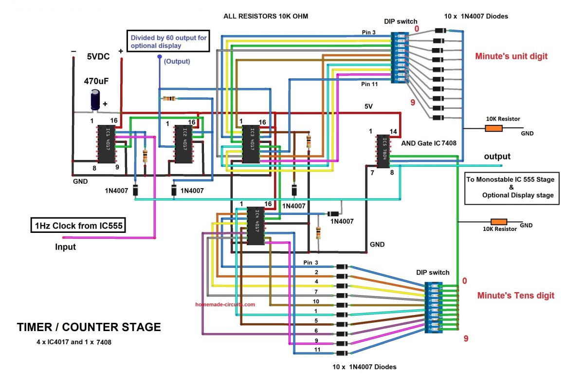 The above circuit is responsible for counting / tracking the time according to astable IC 555��s clock input; the maximum time this circuit can track is 99 minutes.
The above circuit receives 1 Hz clock via pin number 14 (clock input) of IC1 4017 which divides the clock by a factor of 10. The divided clock cycle is outputted at carry-out pin, which is pin number 12.
The IC2 4017 is cascaded with IC1 and it receives the clock pulse from pin 12 of IC1. The IC2 is configured to divide the input clock by a factor of 6; this is achieved by connecting the reset pin number 15 to 6th sequential output of IC2 which is pin number 5. Now at pin number 5 we will get 1 pulse for every minute.
The output of IC2 (one pulse per minute) is connect to IC3 which divides the output by a factor of 10 which gives us unit digit of a minute.
The IC3��s carry-out signal is fed to pin number 14 of IC4 4017 which gives us tens digit of the minute.
The output of IC3 and IC4 is fed to logic AND gate IC 7408 via two DIP switches which is used for setting the time for activating the bell.
When the logic gate��s inputs receive as high the output turns high which triggers the next stage.
There are 10 diodes at each DIP switches to prevent short circuit between output pins of IC 4017s which could occur when you accidently turn ON two or more dip switches simultaneously.
The output of AND gate is not only fed to the next stage but also fed to reset pins of all IC 4017s via diodes, so that when the desired time is reached, all the IC 4017��s count resets to zero.
NOTE: Both the DIP switches scales from 0 to 9, one for unit digit and one for tens digit.
Example: Say you want to activate the bell for every 45 minute, slid the 5th DIP switch ON for units digit and 4th DIP switch ON for tens digit.
Pin diagram of IC 4017 and IC 4026:
The above circuit is responsible for counting / tracking the time according to astable IC 555��s clock input; the maximum time this circuit can track is 99 minutes.
The above circuit receives 1 Hz clock via pin number 14 (clock input) of IC1 4017 which divides the clock by a factor of 10. The divided clock cycle is outputted at carry-out pin, which is pin number 12.
The IC2 4017 is cascaded with IC1 and it receives the clock pulse from pin 12 of IC1. The IC2 is configured to divide the input clock by a factor of 6; this is achieved by connecting the reset pin number 15 to 6th sequential output of IC2 which is pin number 5. Now at pin number 5 we will get 1 pulse for every minute.
The output of IC2 (one pulse per minute) is connect to IC3 which divides the output by a factor of 10 which gives us unit digit of a minute.
The IC3��s carry-out signal is fed to pin number 14 of IC4 4017 which gives us tens digit of the minute.
The output of IC3 and IC4 is fed to logic AND gate IC 7408 via two DIP switches which is used for setting the time for activating the bell.
When the logic gate��s inputs receive as high the output turns high which triggers the next stage.
There are 10 diodes at each DIP switches to prevent short circuit between output pins of IC 4017s which could occur when you accidently turn ON two or more dip switches simultaneously.
The output of AND gate is not only fed to the next stage but also fed to reset pins of all IC 4017s via diodes, so that when the desired time is reached, all the IC 4017��s count resets to zero.
NOTE: Both the DIP switches scales from 0 to 9, one for unit digit and one for tens digit.
Example: Say you want to activate the bell for every 45 minute, slid the 5th DIP switch ON for units digit and 4th DIP switch ON for tens digit.
Pin diagram of IC 4017 and IC 4026:
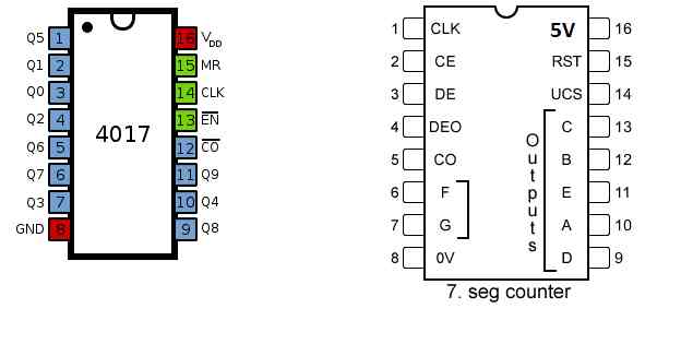
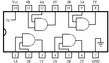 Monostable multivibrator stage:
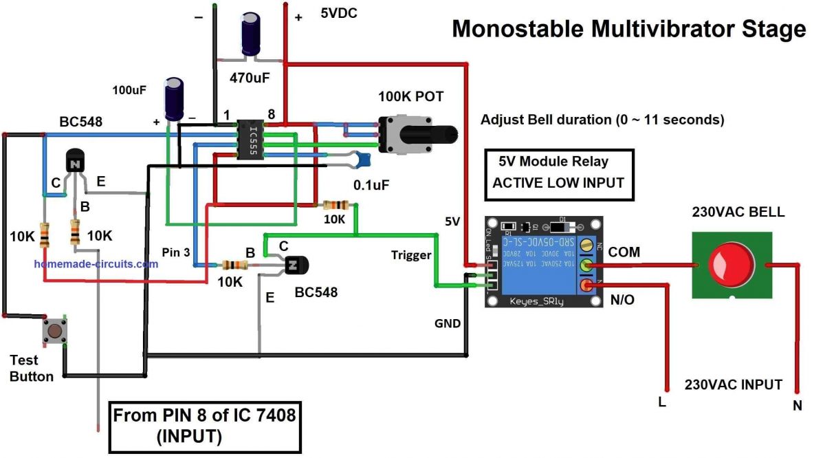 The above circuit consists of an IC 555 which is configured as monostable multivibrator.
This stage is responsible for activating the bell for a predetermined period of time in seconds by adjusting the provided 100K potentiometer.
You can set the time from 0 to 11 seconds maximum after which the bell deactivates.
The circuit receives its trigger signal from AND gate��s output.
The signal is received by an NPN transistor at left most side (of the diagram) inverts the signal to negative pulse which is necessary to trigger the IC 555.
A test button is provided to test the duration of the bell ring while adjusting the potentiometer and also for regular maintenance / debugging the circuit.
A 5V relay module is employed to trigger the 230 VAC bell.
The relay must be a low level trigger type to work with the circuit.
A transistor is connect at pin 3 of IC 555 to trigger the relay and the transistor is here to invert the IC 555��s output signal from positive pulse to negative pulse.
The above circuit consists of an IC 555 which is configured as monostable multivibrator.
This stage is responsible for activating the bell for a predetermined period of time in seconds by adjusting the provided 100K potentiometer.
You can set the time from 0 to 11 seconds maximum after which the bell deactivates.
The circuit receives its trigger signal from AND gate��s output.
The signal is received by an NPN transistor at left most side (of the diagram) inverts the signal to negative pulse which is necessary to trigger the IC 555.
A test button is provided to test the duration of the bell ring while adjusting the potentiometer and also for regular maintenance / debugging the circuit.
A 5V relay module is employed to trigger the 230 VAC bell.
The relay must be a low level trigger type to work with the circuit.
A transistor is connect at pin 3 of IC 555 to trigger the relay and the transistor is here to invert the IC 555��s output signal from positive pulse to negative pulse.
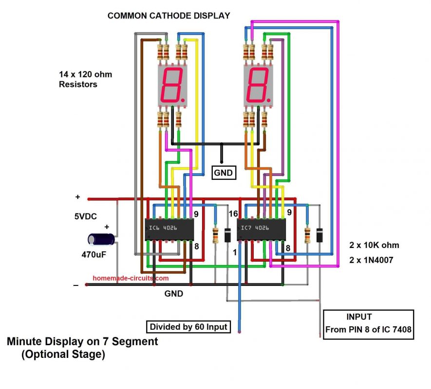 The above circuit stage is optional for displaying minutes by tracking the clock cycle from IC2 4017 which outputs 1 clock cycle per minute.
When the bell gets activated the display resets to zero and counts the time again.
The circuit consists of just two IC 4026s which are used for driving common cathode 7 segment displays.
The two ICs are cascaded to count from 00 to 99 and the clock input is fed through pin 1 of IC7 and the carry-out is at pin 5, which is fed to IC6��s clock input pin 1. Resetting the digits to 00 is achieved by feeding AND gate��s output to pin 15 of both the IC 4026 through a diode.
The above circuit stage is optional for displaying minutes by tracking the clock cycle from IC2 4017 which outputs 1 clock cycle per minute.
When the bell gets activated the display resets to zero and counts the time again.
The circuit consists of just two IC 4026s which are used for driving common cathode 7 segment displays.
The two ICs are cascaded to count from 00 to 99 and the clock input is fed through pin 1 of IC7 and the carry-out is at pin 5, which is fed to IC6��s clock input pin 1. Resetting the digits to 00 is achieved by feeding AND gate��s output to pin 15 of both the IC 4026 through a diode.
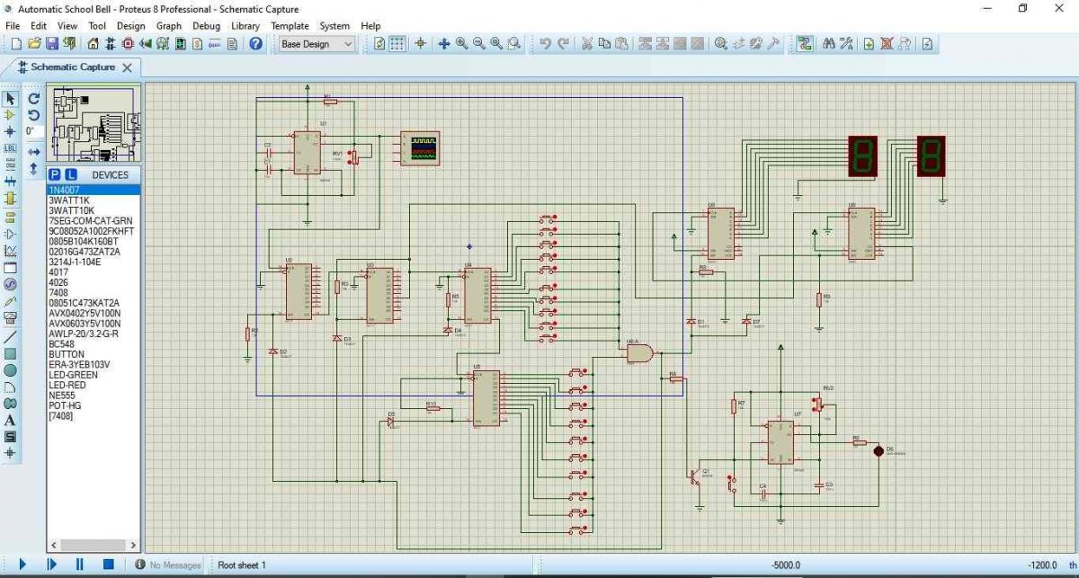 IC 555 clock generator:
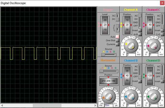 In the simulation you may set the IC 555��s output to more than 1 Hz to see the intended result faster by adjusting the pot to minimum position as illustrated below.
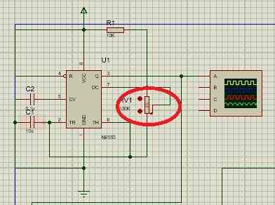
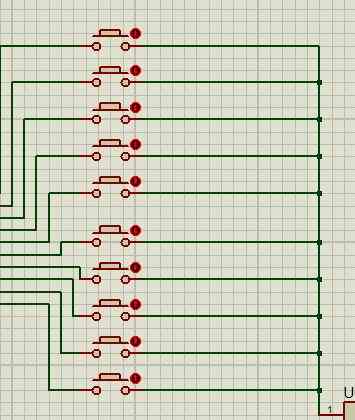 You can see minutes on the 7 segment display as illustrated below:
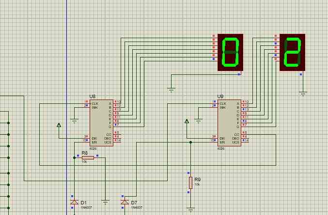 Download the Simulation files from the below given link:
SimulationDownload
Download the Simulation files from the below given link:
SimulationDownload
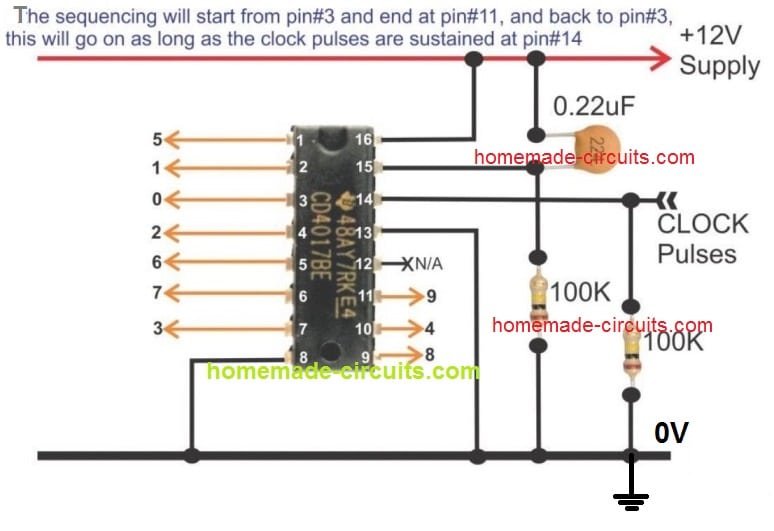
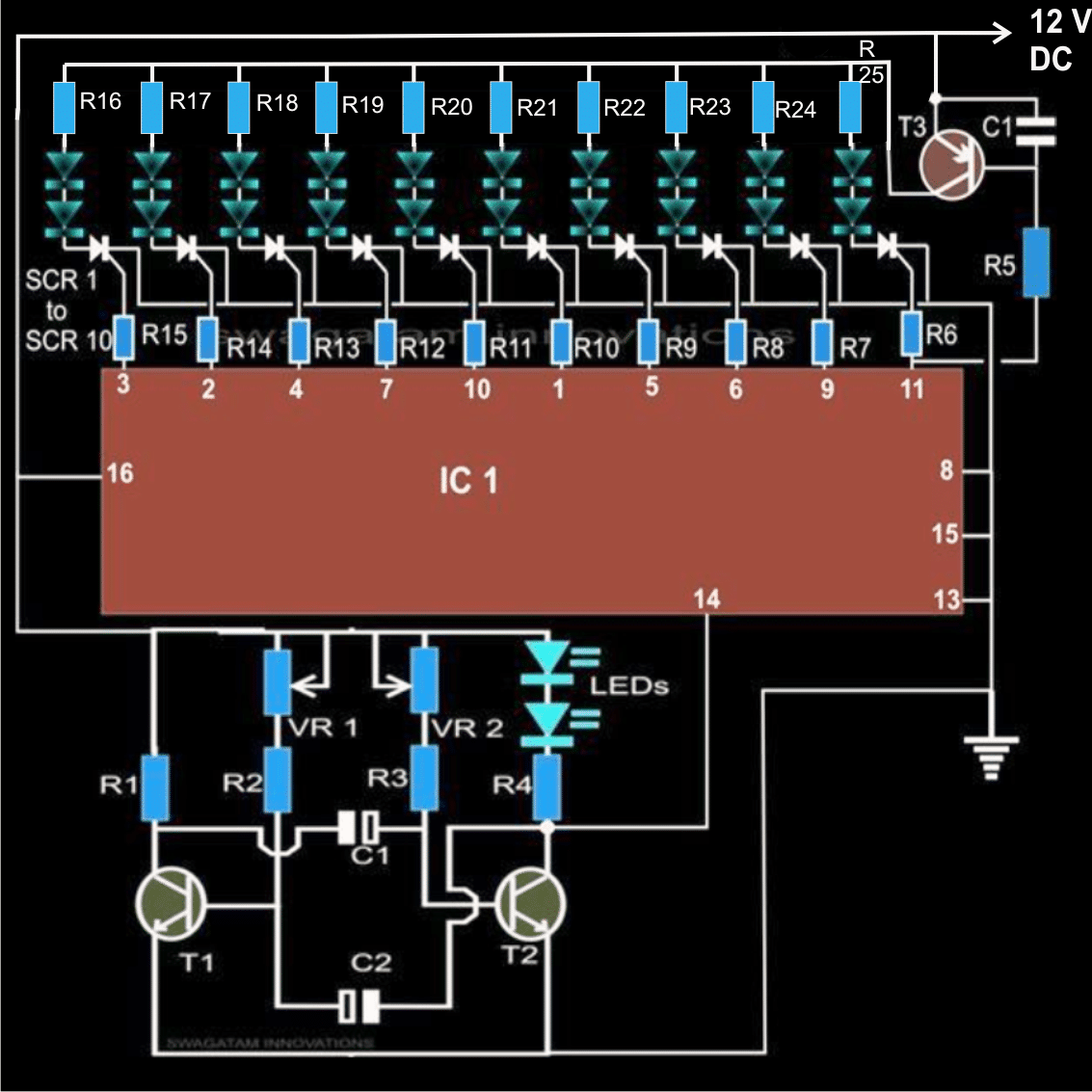
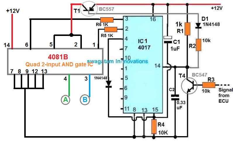

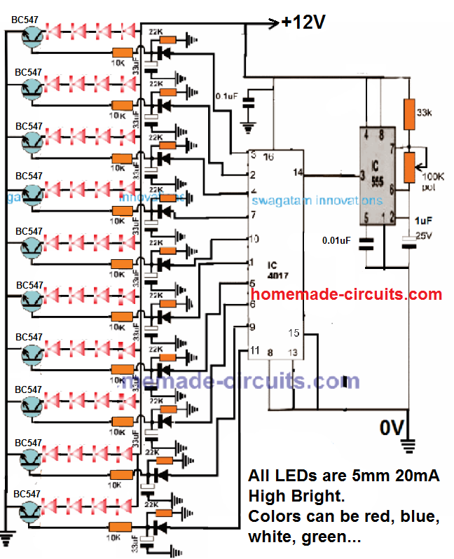

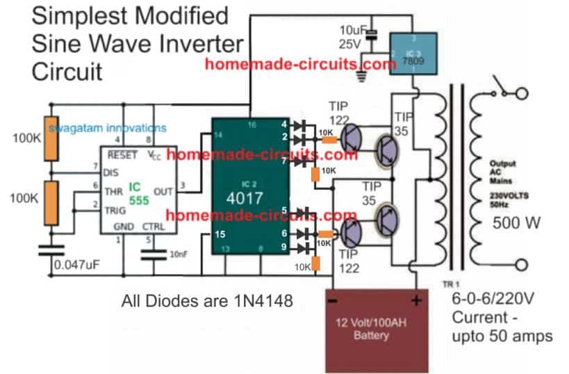
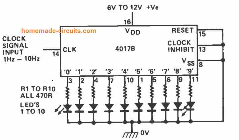 Reversing the polarity of all LEDs and connecting their common point to the positive supply line produces an alternate action in which nine LEDs are on and one is off at any one instant, and advances in response to the clock pulses at pin#14.
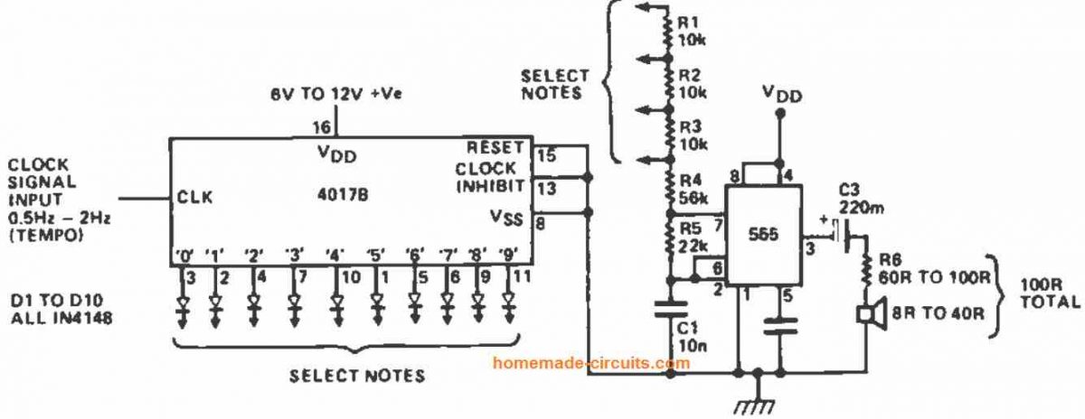 A desired musical tune or melody may be generated with this circuit of a 10-stage 4-note musical sequencer.
Several moreresistors can be added to the R1-R4 networkchain to maximize the number of accessible notes.
A desired musical tune or melody may be generated with this circuit of a 10-stage 4-note musical sequencer.
Several moreresistors can be added to the R1-R4 networkchain to maximize the number of accessible notes.
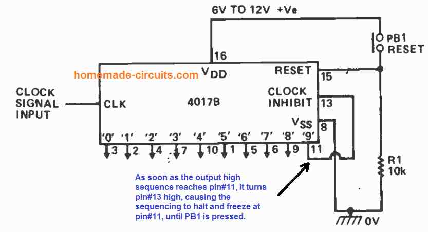 The above 4017 circuit demonstrates a simple wayto wire the 4017 such the counting freezesafter a preset counting sequence.
The counter is configured to halt as soon asthe "9" output drives the clock inhibit pin#13high.
By pushing the reset switch PB1, the counting sequence could be reinitialized.
This also means that, by connecting any other desired output pin with pin#13., the sequencing could be made to halt on that specific output pin.
More of these projects can be found under the following Link:
The above 4017 circuit demonstrates a simple wayto wire the 4017 such the counting freezesafter a preset counting sequence.
The counter is configured to halt as soon asthe "9" output drives the clock inhibit pin#13high.
By pushing the reset switch PB1, the counting sequence could be reinitialized.
This also means that, by connecting any other desired output pin with pin#13., the sequencing could be made to halt on that specific output pin.
More of these projects can be found under the following Link:

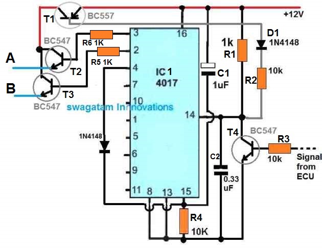 1) As soon as the circuit is powered from the 12V battery, the IC 4017 is reset through C1.
2) Pin3 of the IC now becomes high, and T2 gets into the standby condition with its base biased with the pin3 voltage.
But T2 cannot conduct as yet due to the absence of a voltage on its collector pin.
3) When the first ECU pulse arrives at the base of T4, it is turned ON, and T4 grounds pin14 of the IC.
But the IC does not respond to this since it is designed to respond only to positive pulses at pin14 and not to negative pulses.
4) However, during the time T4 conducts, T1 is also turned ON, due to its base getting the negative bias via D1, R2, T4. In the process T1 transfers the + 12V to the collector of T2, until the voltage is transferred to its emitter, and topoint A
5) Next, the ECU pulse switches OFF, causing T4 to switch OFF, which instantly causes a positive pulse to generate at pin14 via R1.
6) At this point, the IC 4017 responds and causes the logic high from pin3 to jump to pin2.
7) Now, pin2 gets into the standby mode, waiting for the next pulse from the ECU.
8) When the next ECU pulse arrives, the above procedure repeats, until the ECU pulse turns OFF, which in turn causes the logic high from pin2 of the IC to jump to pin4. Simultaneously, the point B is also fired via the emitter of T3.
9) The moment the logic high reaches pin4, the IC gets instantly reset, causing the logic high to return to pin3.
10) The circuit now reaches its earlier position waiting for the next repetition.
1) As soon as the circuit is powered from the 12V battery, the IC 4017 is reset through C1.
2) Pin3 of the IC now becomes high, and T2 gets into the standby condition with its base biased with the pin3 voltage.
But T2 cannot conduct as yet due to the absence of a voltage on its collector pin.
3) When the first ECU pulse arrives at the base of T4, it is turned ON, and T4 grounds pin14 of the IC.
But the IC does not respond to this since it is designed to respond only to positive pulses at pin14 and not to negative pulses.
4) However, during the time T4 conducts, T1 is also turned ON, due to its base getting the negative bias via D1, R2, T4. In the process T1 transfers the + 12V to the collector of T2, until the voltage is transferred to its emitter, and topoint A
5) Next, the ECU pulse switches OFF, causing T4 to switch OFF, which instantly causes a positive pulse to generate at pin14 via R1.
6) At this point, the IC 4017 responds and causes the logic high from pin3 to jump to pin2.
7) Now, pin2 gets into the standby mode, waiting for the next pulse from the ECU.
8) When the next ECU pulse arrives, the above procedure repeats, until the ECU pulse turns OFF, which in turn causes the logic high from pin2 of the IC to jump to pin4. Simultaneously, the point B is also fired via the emitter of T3.
9) The moment the logic high reaches pin4, the IC gets instantly reset, causing the logic high to return to pin3.
10) The circuit now reaches its earlier position waiting for the next repetition.
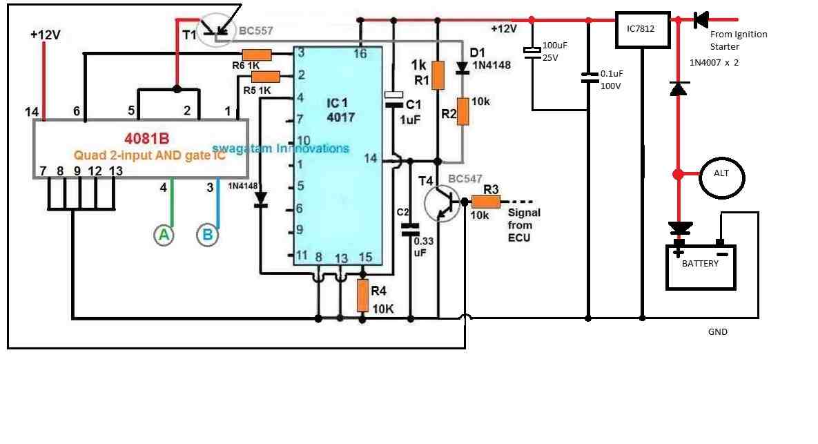
 The idea was requested by one of the avid readers of this blog.
Here's the required working concept.
The idea was requested by one of the avid readers of this blog.
Here's the required working concept.
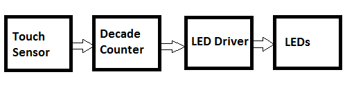 The touch sensor converts the tiny finger touch signal into amplified electrical pulses.
The next decade counter stage converts these pulses into shifting logic levels across its outputs.
These shifting logic pulses are fed to the corresponding LED drivers which convert these signals into a sequentially varying voltages for the LED stage.
The varying voltages from the transistor stage which are set at specified levels cause the LEDs to illuminate with different light levels or brightness., accomplishing the dimmable effect on the LEDs.
The touch sensor converts the tiny finger touch signal into amplified electrical pulses.
The next decade counter stage converts these pulses into shifting logic levels across its outputs.
These shifting logic pulses are fed to the corresponding LED drivers which convert these signals into a sequentially varying voltages for the LED stage.
The varying voltages from the transistor stage which are set at specified levels cause the LEDs to illuminate with different light levels or brightness., accomplishing the dimmable effect on the LEDs.
 Indian subcontinent is a land of festivals and celebrations which mostly start from the month of August and continues until the New Year.
All these festivals have one fundamental thing in common, and that is dazzling colorful lights, flashing and running with all sorts of patterns and sequences.
Most of these lights are in the form of LED lights since LEDs are the most efficient in terms of brightness and cost.
In this article we will discuss one such interesting LED ornamental project, which will imitate a rotating illuminated chakra light.
These can be commonly seen behind the crown of popular God idols like lord Ganesha, Sai baba, and around the finger of Lord Vishnu.
Indian subcontinent is a land of festivals and celebrations which mostly start from the month of August and continues until the New Year.
All these festivals have one fundamental thing in common, and that is dazzling colorful lights, flashing and running with all sorts of patterns and sequences.
Most of these lights are in the form of LED lights since LEDs are the most efficient in terms of brightness and cost.
In this article we will discuss one such interesting LED ornamental project, which will imitate a rotating illuminated chakra light.
These can be commonly seen behind the crown of popular God idols like lord Ganesha, Sai baba, and around the finger of Lord Vishnu.

 The fan regulator can be connected anywhere in series with the wiring.
Any light bulb can be connected with the clap switch relay as given in the folowing figure
The fan regulator can be connected anywhere in series with the wiring.
Any light bulb can be connected with the clap switch relay as given in the folowing figure
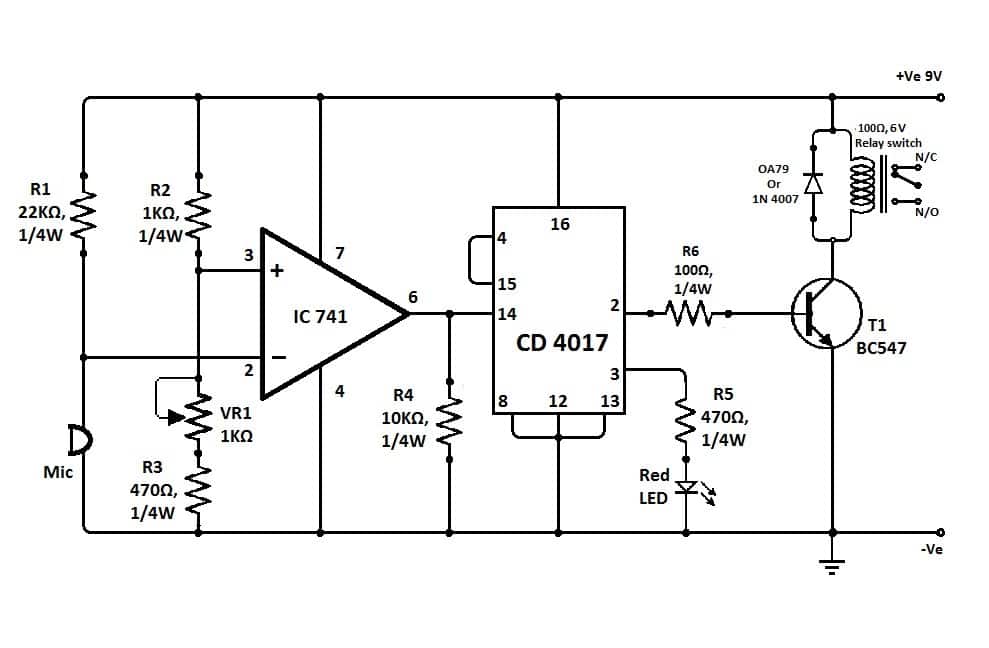 The above clap operated relay circuit was provided to me by one of the keen readers of this blog Mr.
Dathan.
The circuit is very to understand:
The opamp here is configured as a comparator, meaning it is positioned to differentiate the slightest of voltage differences across its two inputs.
When the clap sound hits the mic, a momentary drop of voltage is experienced at pin#2 of the IC, this situation raises the voltage at pin#3 of the IC for that instant.
As we know, with pin#3 at higher potential than pin#2 makes the output of the IC high, the condition puts the output of the IC go high momentarily.
This high response triggers the IC 4017 pin#14, and forces its output to either move from pin#2 to pin#3 or vice versa depending upon the initial situation of the outputs.
The above action switches the load accordingly either to ON or OFF position.
The above 12 V clap triggered switch circuit using IC 741 was successfully tried and tested by Mr.
Ajay Dussa.
The following prototype images for the same were sent by Mr.
Ajay.
The above clap operated relay circuit was provided to me by one of the keen readers of this blog Mr.
Dathan.
The circuit is very to understand:
The opamp here is configured as a comparator, meaning it is positioned to differentiate the slightest of voltage differences across its two inputs.
When the clap sound hits the mic, a momentary drop of voltage is experienced at pin#2 of the IC, this situation raises the voltage at pin#3 of the IC for that instant.
As we know, with pin#3 at higher potential than pin#2 makes the output of the IC high, the condition puts the output of the IC go high momentarily.
This high response triggers the IC 4017 pin#14, and forces its output to either move from pin#2 to pin#3 or vice versa depending upon the initial situation of the outputs.
The above action switches the load accordingly either to ON or OFF position.
The above 12 V clap triggered switch circuit using IC 741 was successfully tried and tested by Mr.
Ajay Dussa.
The following prototype images for the same were sent by Mr.
Ajay.
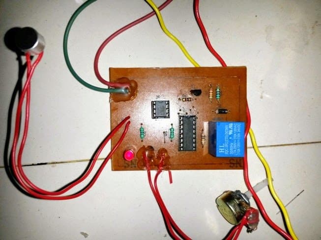 The PCB design (track layout) for the above can be seen below, as designed by Mr.
Ajay:
The PCB design (track layout) for the above can be seen below, as designed by Mr.
Ajay:

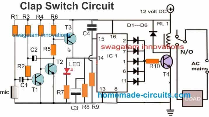 Clap Switch Video Demonstration
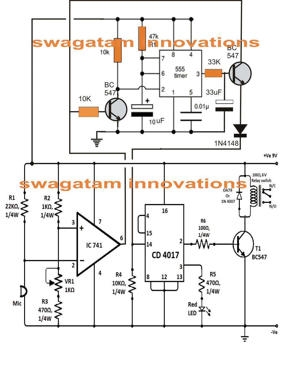
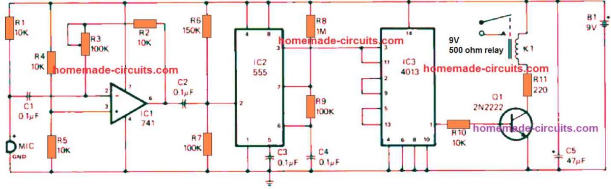 The first sharp hand clap is detected by the electret microphone and is fed into operational amplifier ICI's inverting ( -) input at pin 2 via C1. The signal negative peak at the pin 6 output of IC1 subsequently activates 555 timer IC2, that is set up like a monostable multivibrator.
The trigger signal reaching the pin 2 input of IC2 is internally extended to toggle the dual D flip-flop IC3. With the help of the three-state counter configuration of IC3. Not one but two sharp clap sounds are necessary to create a positive output at pin 1 that causes Q1 into switch ON.
When Q1 activates the relay and switches its contacts to N/O points.
Any electrical appliance attached to the relay's contacts now switches on.
As soon as pin 1 of IC3 becomes high, it continues to be in that situation until a subsequent two powerful hand claps hit the MIC to repeat and revert the condition.
Thus, it requires two loud sound inputs to switch off the electrical load hooked up to the relay's contacts after the circuit is activated.
The first sharp hand clap is detected by the electret microphone and is fed into operational amplifier ICI's inverting ( -) input at pin 2 via C1. The signal negative peak at the pin 6 output of IC1 subsequently activates 555 timer IC2, that is set up like a monostable multivibrator.
The trigger signal reaching the pin 2 input of IC2 is internally extended to toggle the dual D flip-flop IC3. With the help of the three-state counter configuration of IC3. Not one but two sharp clap sounds are necessary to create a positive output at pin 1 that causes Q1 into switch ON.
When Q1 activates the relay and switches its contacts to N/O points.
Any electrical appliance attached to the relay's contacts now switches on.
As soon as pin 1 of IC3 becomes high, it continues to be in that situation until a subsequent two powerful hand claps hit the MIC to repeat and revert the condition.
Thus, it requires two loud sound inputs to switch off the electrical load hooked up to the relay's contacts after the circuit is activated.
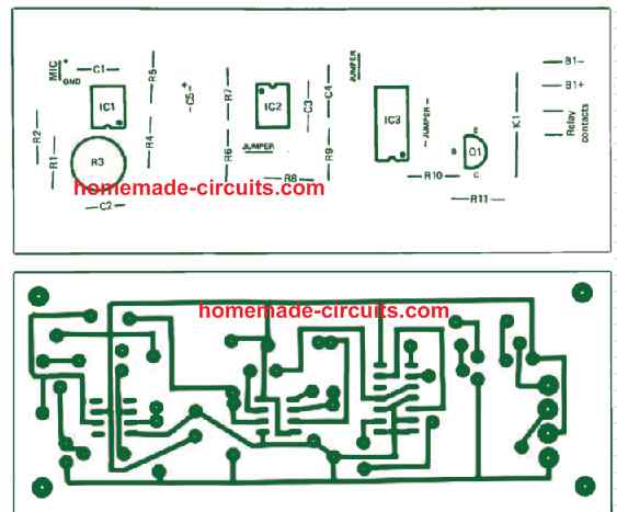

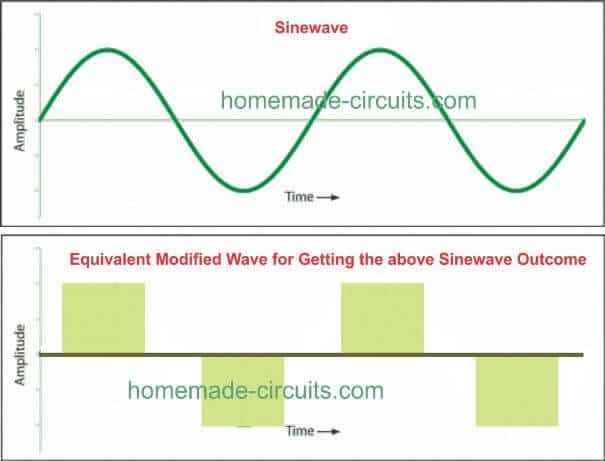
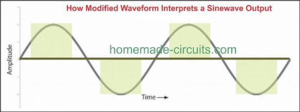 In all the 7 designs explained below we try to implement this theory and ensure that the RMS value of the square waves are appropriate controlled by chopping the 330V peaks into 220V modified RMS.
The same can be applied for 120V AC by chopping down the 160 peaks.
How to Calculate through Easy Formulas
If you are interested to know how to calculate the above modified waveform so that it results in an almost ideal replication of a sinewave, then please refer to the following post for the complete tutorial:
Calculate Modified Square Wave RMS Sine Equivalent Value
In all the 7 designs explained below we try to implement this theory and ensure that the RMS value of the square waves are appropriate controlled by chopping the 330V peaks into 220V modified RMS.
The same can be applied for 120V AC by chopping down the 160 peaks.
How to Calculate through Easy Formulas
If you are interested to know how to calculate the above modified waveform so that it results in an almost ideal replication of a sinewave, then please refer to the following post for the complete tutorial:
Calculate Modified Square Wave RMS Sine Equivalent Value

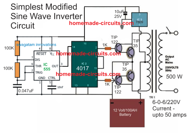 WARNING: PLEASE CONNECT PROTECTION DIODES ACROSS THE COLLECTOR EMITTER OF THE TIP35 TRANSISTOR (CATHODE TO COLLECTOR, ANODE TO EMITTER)
UPDATE: As per the Calculations presented in the this article, the IC 4017 output pins could be ideally configured for achievingan impressive looking modified sinewave inverter.
The modified image can bewitnessedbelow:
WARNING: PLEASE CONNECT PROTECTION DIODES ACROSS THE COLLECTOR EMITTER OF THE TIP35 TRANSISTOR (CATHODE TO COLLECTOR, ANODE TO EMITTER)
UPDATE: As per the Calculations presented in the this article, the IC 4017 output pins could be ideally configured for achievingan impressive looking modified sinewave inverter.
The modified image can bewitnessedbelow:
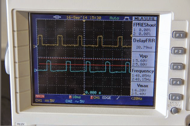 My Reply:
Hello Sarah,
The IC outputs will not show bipolar waves since the signals from these outputs are intended for identical N type transistors and from a single supply....it's the transformer which is responsible for creating the bipolar wave at its output since it's configured with a push-pull topology using a center tap ....so what you are seeing across R4 and R5 are correct waveform.
Please check the waveform at the output of the transformer for verifying the bipolar nature of the waveform.
My Reply:
Hello Sarah,
The IC outputs will not show bipolar waves since the signals from these outputs are intended for identical N type transistors and from a single supply....it's the transformer which is responsible for creating the bipolar wave at its output since it's configured with a push-pull topology using a center tap ....so what you are seeing across R4 and R5 are correct waveform.
Please check the waveform at the output of the transformer for verifying the bipolar nature of the waveform.
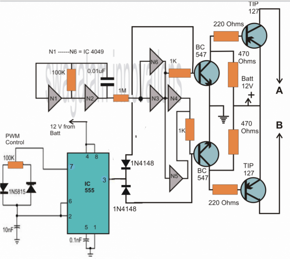
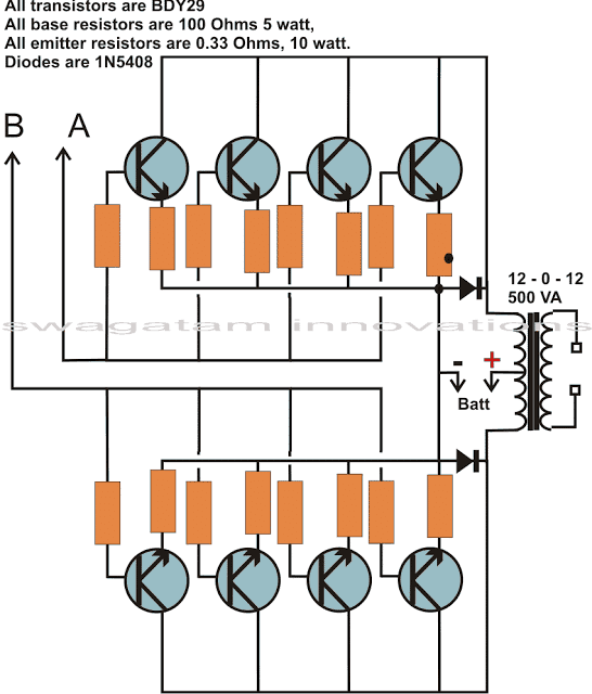 The battery is connected across the center tap and the ground of the transformer and also to the relevant points in the circuit.
Switching ON power immediately starts the inverter, providing rich modified sine wave AC at its output, ready to be used with any load upto 500 VA.
The component details are supplied in the diagram itself.
The above design can also be modified into a 500 watt PWM controlled mosfet sine wave inverter by replacing the driver transistors simply by a few mosfets.
The design shown below would provide about 150 watts of power, for obtaining 500 watts, more number of mosfets may be required to be connected in parallel with the existing two mosfets.
The battery is connected across the center tap and the ground of the transformer and also to the relevant points in the circuit.
Switching ON power immediately starts the inverter, providing rich modified sine wave AC at its output, ready to be used with any load upto 500 VA.
The component details are supplied in the diagram itself.
The above design can also be modified into a 500 watt PWM controlled mosfet sine wave inverter by replacing the driver transistors simply by a few mosfets.
The design shown below would provide about 150 watts of power, for obtaining 500 watts, more number of mosfets may be required to be connected in parallel with the existing two mosfets.
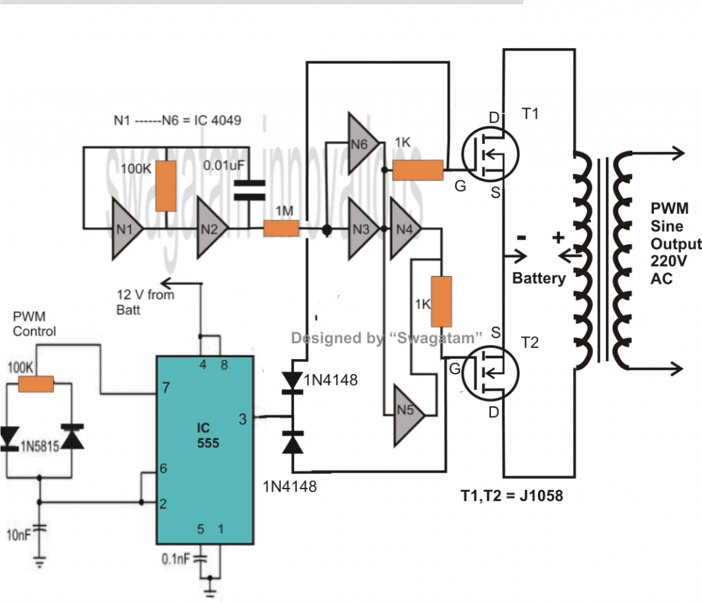
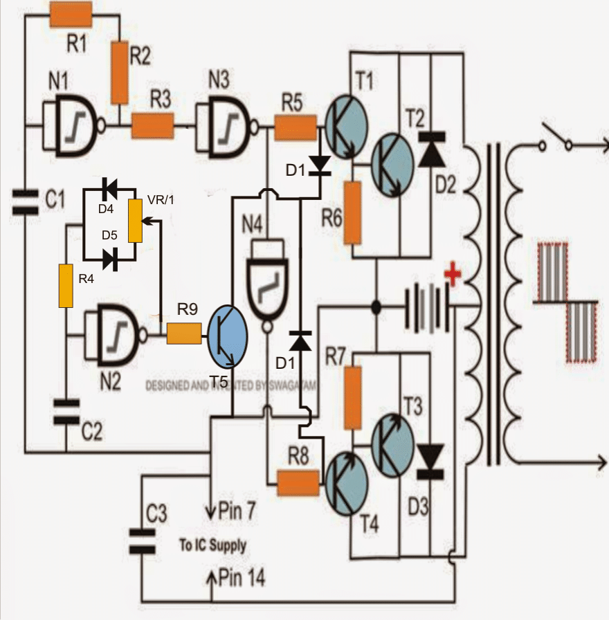
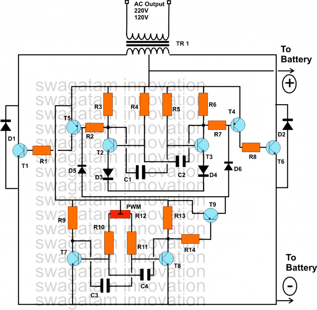
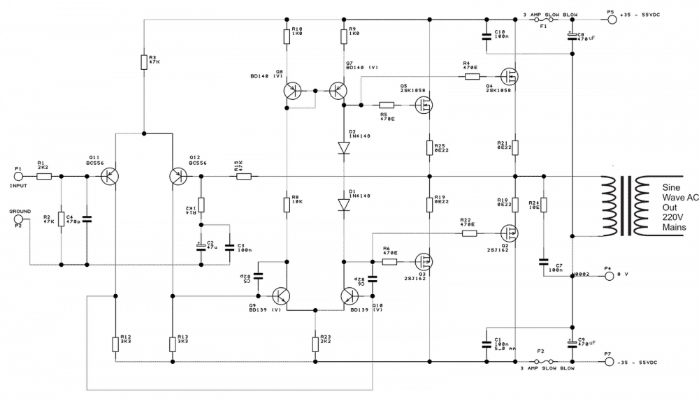
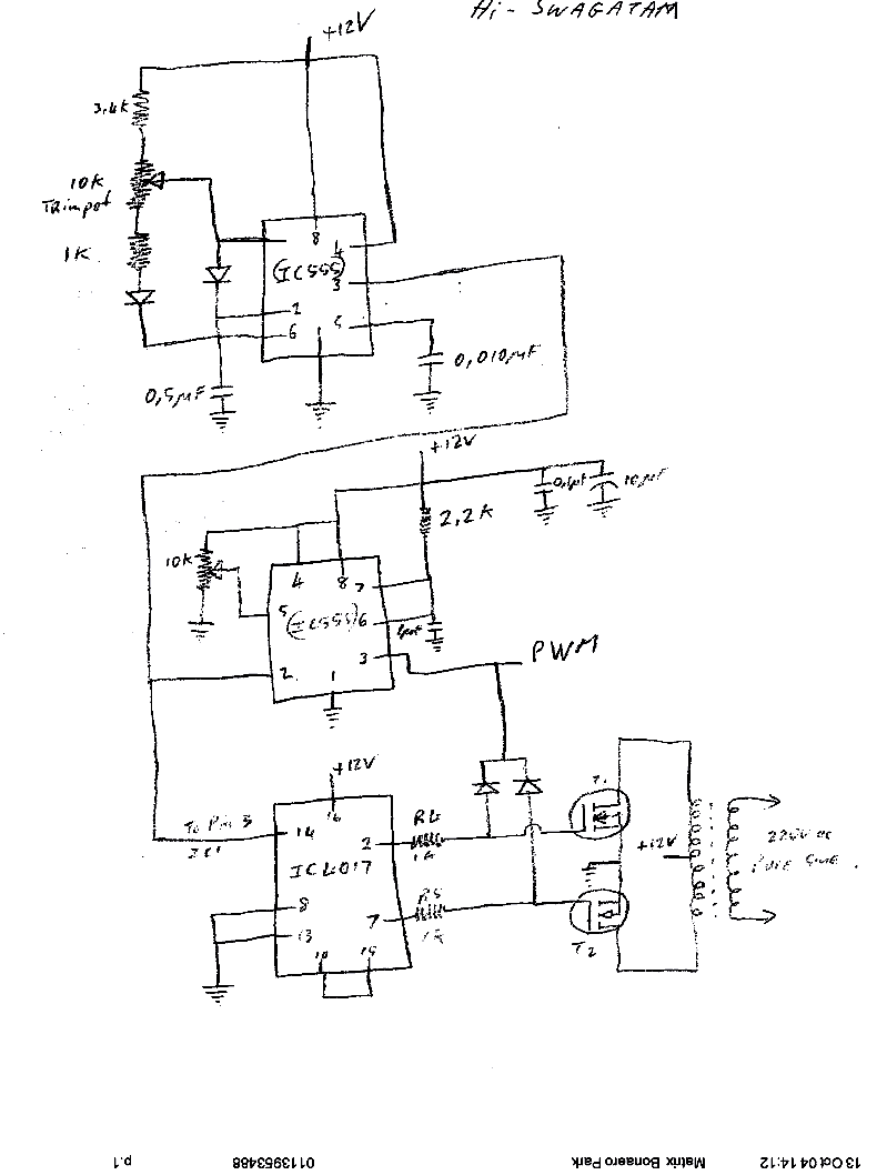


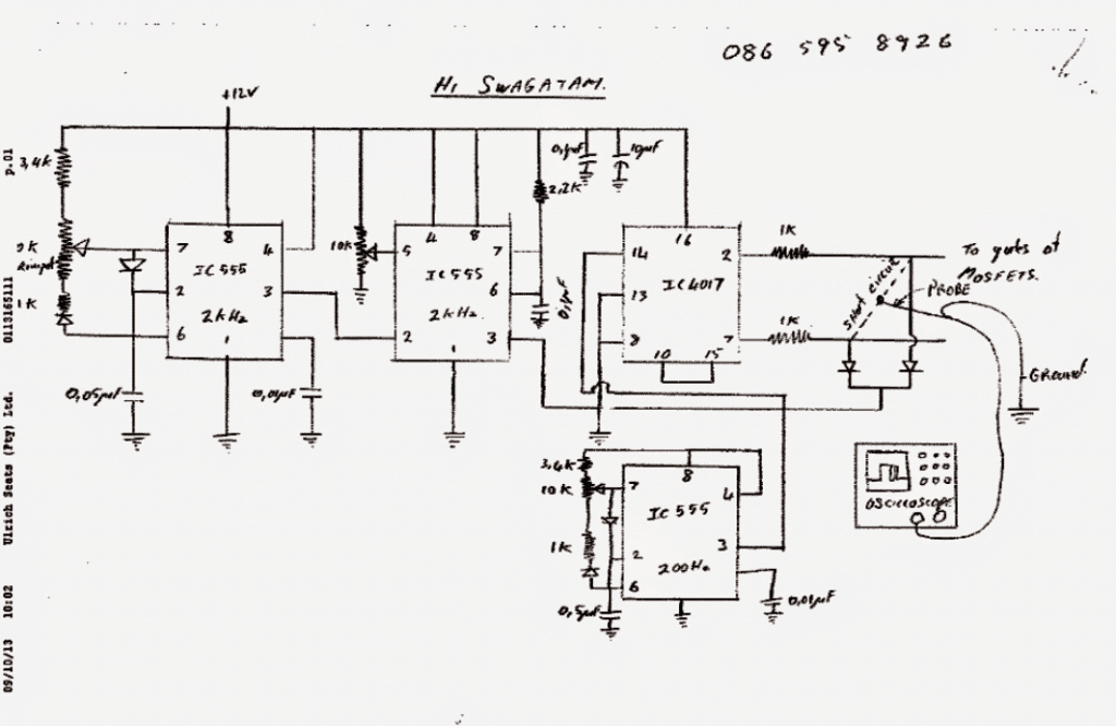


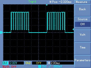


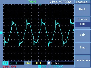
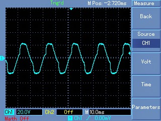
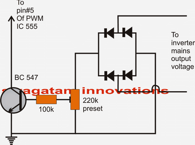
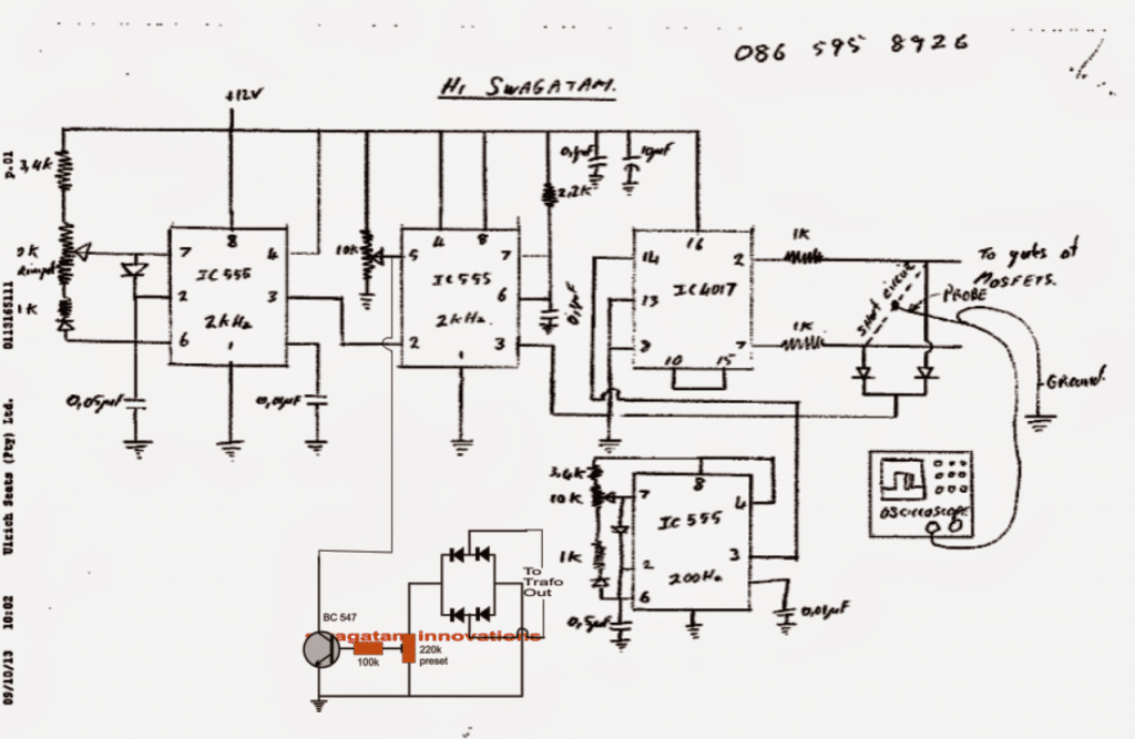
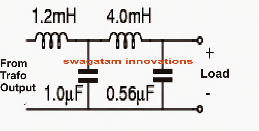
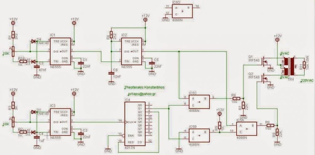 The oscilloscope trace depicts the modified waveform of the inverter across the 10k resistor connected at the mains output of the transformer.
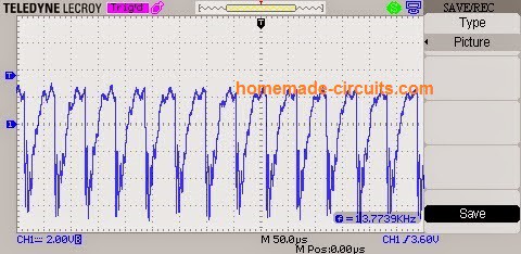 The above modified inverter design by Theofanakis inverter was tested and approved by one of the avid followers of this blog, Mr.
Odon.
The following test images by Odon confirm the sinewave nature of the above inverter circuit.
The above modified inverter design by Theofanakis inverter was tested and approved by one of the avid followers of this blog, Mr.
Odon.
The following test images by Odon confirm the sinewave nature of the above inverter circuit.
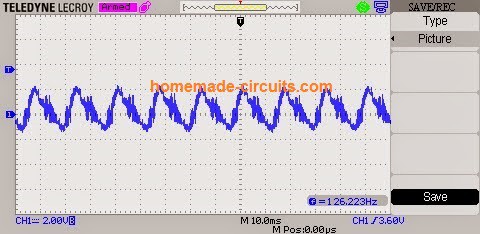
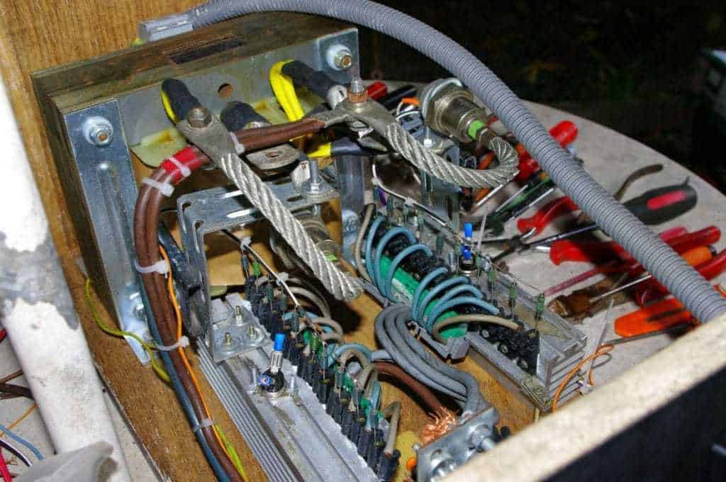
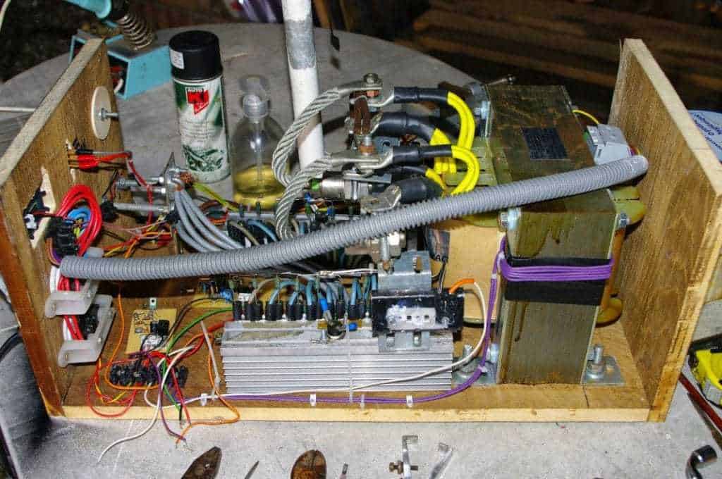
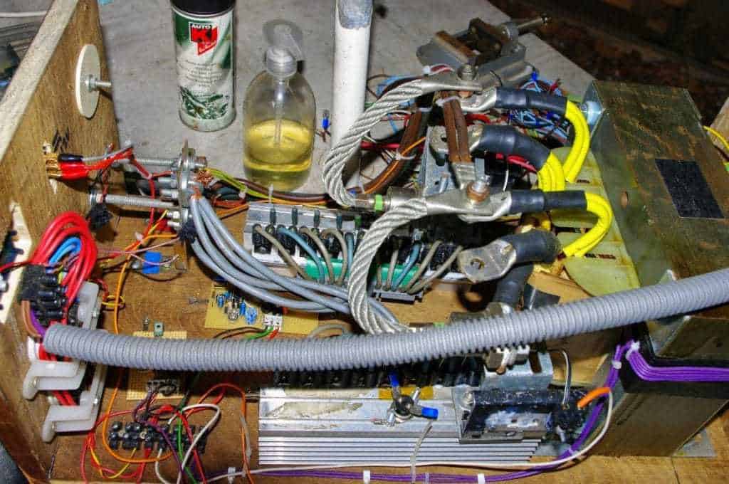
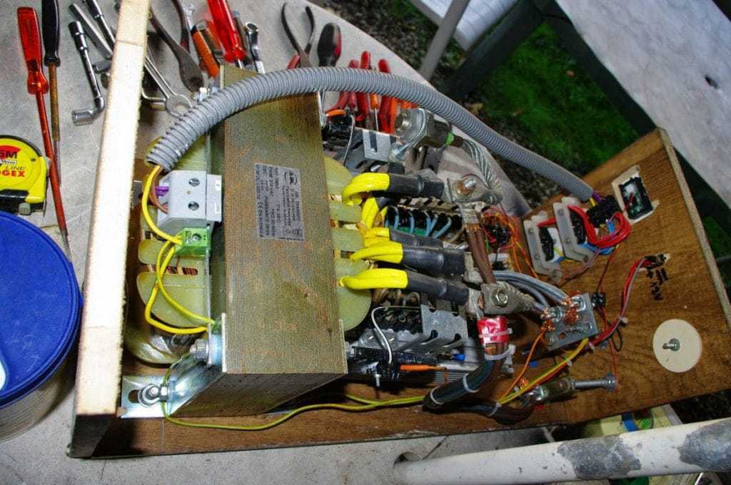
 Note: Mount all the upper TIP36 over a larger finned common heatsink, DO NOT use mica isolator while implementing this.
The same must be done with the lower TIP36 arrays.
But make sure these two heatsinks never touch each other.
The TIP142 transistors must be mounted on separate individual large finned hearsinks.
Note: Mount all the upper TIP36 over a larger finned common heatsink, DO NOT use mica isolator while implementing this.
The same must be done with the lower TIP36 arrays.
But make sure these two heatsinks never touch each other.
The TIP142 transistors must be mounted on separate individual large finned hearsinks.

 Battery Specs:
 The battery can be a standard Li-ion or Lipo Cell rated at 3.7V, 3000mAh.
The Circuit schematic:
The battery can be a standard Li-ion or Lipo Cell rated at 3.7V, 3000mAh.
The Circuit schematic:
 In the figure above we can see the following things:
An appropriately selected spring mechanism attached on the upper surface of a plastic enclosure.
The lower end of the spring is appropriately terminated outside the enclosure with a hook for hanging the drip bottle.
Within the enclosure, the spring end can be seen attached with a permanent magnet, such that under no load the magnet stays in the indicated position, and in the presence of a load which can be a drip bottle filled with the drip liquid, the magnet is displaced to a lower position and away from its original position.
We can also visualize a reed switch positioned near the magnet at its initial no load position.
The reed switch terminals can be seen wired with a circuit assembled over a PCB, and the PCB bolted inside the enclosure as shown in the design.
There are two additional items in the form of a reset push button, a buzzer, and an LED which become the external protruding parts of the PCB.
In the following section we will learn how the above set up works in conjunction with the warning buzzer circuit, inside the enclosure.
In the figure above we can see the following things:
An appropriately selected spring mechanism attached on the upper surface of a plastic enclosure.
The lower end of the spring is appropriately terminated outside the enclosure with a hook for hanging the drip bottle.
Within the enclosure, the spring end can be seen attached with a permanent magnet, such that under no load the magnet stays in the indicated position, and in the presence of a load which can be a drip bottle filled with the drip liquid, the magnet is displaced to a lower position and away from its original position.
We can also visualize a reed switch positioned near the magnet at its initial no load position.
The reed switch terminals can be seen wired with a circuit assembled over a PCB, and the PCB bolted inside the enclosure as shown in the design.
There are two additional items in the form of a reset push button, a buzzer, and an LED which become the external protruding parts of the PCB.
In the following section we will learn how the above set up works in conjunction with the warning buzzer circuit, inside the enclosure.

 The working principle of the drip warning indicator is actually very simple:
Referring to the image above, initially without a filled drip bottle hung, and the circuit powered ON, the circuit stays inactive, but gets into a standby position.
In this position, the magnet stays near the reed switch in the closed position which causes a positive supply at pin#14 of the IC 4017.
However this does not force the IC 4017 to shift its output logic sequence, because simultaneously the supply also resets the pin#15 of the IC through the attached 0.1uF capacitor.
Now, when the drip bottle is attached to the hook, the spring is pulled downward, causing a displacement of the magnet away from the reed switch.
The reed switch instantly opens, removing the positive supply from pin#14 of the IC 4017.
The output of IC 4017 still retains its initial condition, that is the logic stays at the unused pin#3 pinout, due to the negative supply from the 1M resistor.
Let's assume the drip fluid gets used up by the patient, and gradually nears the empty condition.
As soon as this reaches the empty level, the magnet now once again positions itself in its original point where it meets the reed switch.
The reed contacts now closes yet again, causing a positive pulse on pin#14 of IC 4017.
This time the IC reacts to this signal and shifts the high logic from its unused pin#3 to pin#2.
The transistor at pin#2 now activates, and switches ON the buzzer alarm, alerting the concerned member in the vicinity regarding the empty drip bottle.
The LED being in series with the transistor base also lights up providing additional warning indication.
The buzzer continues to buzz and is held in the activated position until the concerned member comes and presses the reset button to revert the circuit in its earlier standby position.
In this position the unit allows the replacement of the empty drip bottle with a fresh filled drip bottle, so that the cycle is able to continue yet again as explained in the above paragraphs.
The working principle of the drip warning indicator is actually very simple:
Referring to the image above, initially without a filled drip bottle hung, and the circuit powered ON, the circuit stays inactive, but gets into a standby position.
In this position, the magnet stays near the reed switch in the closed position which causes a positive supply at pin#14 of the IC 4017.
However this does not force the IC 4017 to shift its output logic sequence, because simultaneously the supply also resets the pin#15 of the IC through the attached 0.1uF capacitor.
Now, when the drip bottle is attached to the hook, the spring is pulled downward, causing a displacement of the magnet away from the reed switch.
The reed switch instantly opens, removing the positive supply from pin#14 of the IC 4017.
The output of IC 4017 still retains its initial condition, that is the logic stays at the unused pin#3 pinout, due to the negative supply from the 1M resistor.
Let's assume the drip fluid gets used up by the patient, and gradually nears the empty condition.
As soon as this reaches the empty level, the magnet now once again positions itself in its original point where it meets the reed switch.
The reed contacts now closes yet again, causing a positive pulse on pin#14 of IC 4017.
This time the IC reacts to this signal and shifts the high logic from its unused pin#3 to pin#2.
The transistor at pin#2 now activates, and switches ON the buzzer alarm, alerting the concerned member in the vicinity regarding the empty drip bottle.
The LED being in series with the transistor base also lights up providing additional warning indication.
The buzzer continues to buzz and is held in the activated position until the concerned member comes and presses the reset button to revert the circuit in its earlier standby position.
In this position the unit allows the replacement of the empty drip bottle with a fresh filled drip bottle, so that the cycle is able to continue yet again as explained in the above paragraphs.


 The image above clearly shows, that the IR beam from the Tx must be pulsed with the center frequency of the IC which is generally between 30kHz and 39kHx, and modulated with bursts of 10ms gap.
The TSOP responds to this center frequency signal and triggers ON, producing a replicated waveform at its output, wherein the 38kHz are leveled out into bursts of ordinary square wave pulses.
This complex operational waveform ensures increased immunity against many spurious frequencies that may be present in the atmosphere emanated from light bulbs, lke CFLs, fluorescent lamps etc.
The image above clearly shows, that the IR beam from the Tx must be pulsed with the center frequency of the IC which is generally between 30kHz and 39kHx, and modulated with bursts of 10ms gap.
The TSOP responds to this center frequency signal and triggers ON, producing a replicated waveform at its output, wherein the 38kHz are leveled out into bursts of ordinary square wave pulses.
This complex operational waveform ensures increased immunity against many spurious frequencies that may be present in the atmosphere emanated from light bulbs, lke CFLs, fluorescent lamps etc.
 The 6 gates are all from the IC 4049, R3 can be 10K resistors while the presets can be 100K.
The C1 caps will need to be selected with some practical experimentation.
The diode can be a 1N4148, remaining resistors may be selected 2K2.
As can be seen the upper pair of gates along with R3, preset and C1 is configured as a free running oscillator, the lower section also has an identical stage.
The upper section is fed to an intermediate buffer gate whose output is finally connected with the transmitter IR photodiode.
The whole section is configured to generate the basic center frequency for the TSOP17XX compatibility which may range from 32kHz to 38kHz depending on the spec of the selected sensor.
The lower oscillator is supposed to be a low frequency modulating stage which can be seen integrated with the upper section through a diode.
This low frequency switches the upper high frequency to generate the required "38kHz bursts" on the IR transmitter diode.
This low frequency actually becomes our unique frequency, or the intended customized remote control frequency which needs to be matched with the LM567 frequency so that the both frequencies "shake hands" during the IR communication between the Tx and the Rx units.
The low frequency could be selected from anywhere between 1kHz to 10kHz, and this selected range should be precisely set for the LM567 stage by appropriately adjusting its R1/C1 values.
This concludes our discussion regarding how to modify a TSOP17XX sensor circuit for accommodating customized special frequency ranges or uniquely selected frequency ranges for making the remote control system absolutely foolproof and personal.
If you have any doubts regarding the concept, the comment box is all yours!
The 6 gates are all from the IC 4049, R3 can be 10K resistors while the presets can be 100K.
The C1 caps will need to be selected with some practical experimentation.
The diode can be a 1N4148, remaining resistors may be selected 2K2.
As can be seen the upper pair of gates along with R3, preset and C1 is configured as a free running oscillator, the lower section also has an identical stage.
The upper section is fed to an intermediate buffer gate whose output is finally connected with the transmitter IR photodiode.
The whole section is configured to generate the basic center frequency for the TSOP17XX compatibility which may range from 32kHz to 38kHz depending on the spec of the selected sensor.
The lower oscillator is supposed to be a low frequency modulating stage which can be seen integrated with the upper section through a diode.
This low frequency switches the upper high frequency to generate the required "38kHz bursts" on the IR transmitter diode.
This low frequency actually becomes our unique frequency, or the intended customized remote control frequency which needs to be matched with the LM567 frequency so that the both frequencies "shake hands" during the IR communication between the Tx and the Rx units.
The low frequency could be selected from anywhere between 1kHz to 10kHz, and this selected range should be precisely set for the LM567 stage by appropriately adjusting its R1/C1 values.
This concludes our discussion regarding how to modify a TSOP17XX sensor circuit for accommodating customized special frequency ranges or uniquely selected frequency ranges for making the remote control system absolutely foolproof and personal.
If you have any doubts regarding the concept, the comment box is all yours!
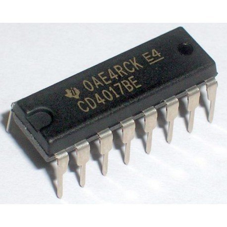
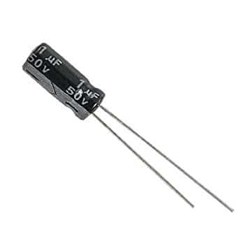
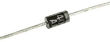
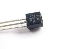
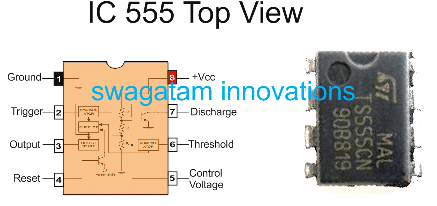
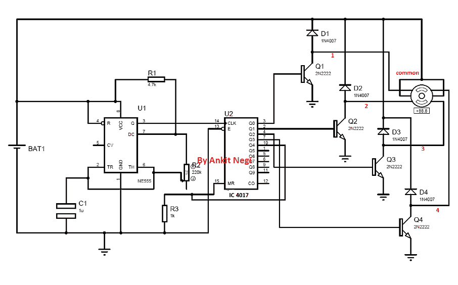 Make connections as shown in figure.
1. Connect pin 3 or output pin of 555 timer to pin 14 (clock pin ) of IC 4017.
2. Connect enable pin or 13th pin of 4017 to ground.
3. Connect pins 3,2,4,7 one by one to transistors 1,2,3,4 respectively.
4. Connect 10 and 15th pin to ground through a 1k resistor.
5. Connect common wire of stepper motor to the positive of supply.
6. Connect other wires of stepper motor in such a way so that coils are energized one by one to complete one full revolution properly.( you can look into datasheet of the motor provided by the manufacturer)
Make connections as shown in figure.
1. Connect pin 3 or output pin of 555 timer to pin 14 (clock pin ) of IC 4017.
2. Connect enable pin or 13th pin of 4017 to ground.
3. Connect pins 3,2,4,7 one by one to transistors 1,2,3,4 respectively.
4. Connect 10 and 15th pin to ground through a 1k resistor.
5. Connect common wire of stepper motor to the positive of supply.
6. Connect other wires of stepper motor in such a way so that coils are energized one by one to complete one full revolution properly.( you can look into datasheet of the motor provided by the manufacturer)

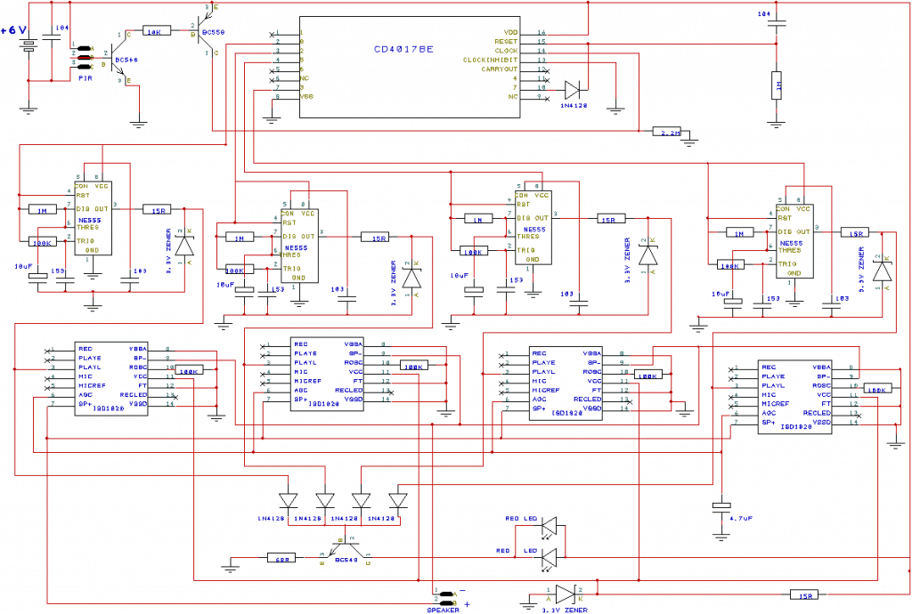 This is my PCB.I have jumper wires connecting A to A , B to B��..,3 to 3,2 to 2��.
and so forth.
It seems to work pretty well, but I wonder ifthere is a better design.
Thanks for your help!
Norman Kelley
This is my PCB.I have jumper wires connecting A to A , B to B��..,3 to 3,2 to 2��.
and so forth.
It seems to work pretty well, but I wonder ifthere is a better design.
Thanks for your help!
Norman Kelley
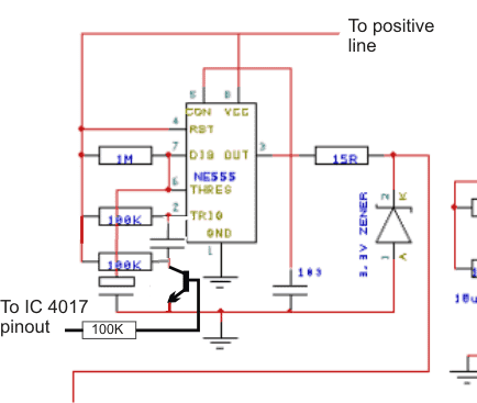 Now this looks much better, here the supply to the monostable is acquired from the circuits +/- DC power rails, while the triggering is acquired from the relevant IC 4017 pinout at pin#2 of the monostable.
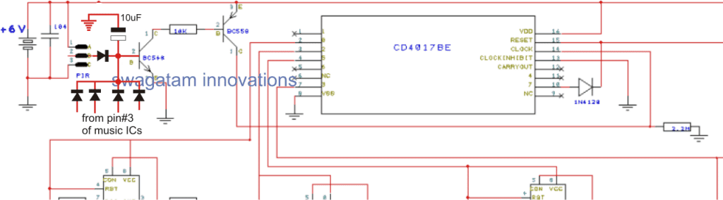 Here only the 4017 IC is powered from the 6V battery terminals while the rest of the circuit stages are powered from the collector of PIR PNP transistor BC559.
The idea is simple, the moment a human presence is detected, the PIR gets activated and powers the monostable along the message player circuit stages, the message player circuit responds to this and starts playing the recorded clip.
This audio signal is sent back to the PIR NPN transistor base and latches it ON so that now the entire circuit is able to remain powered as long as the message is being played.
The moment the message player completes playing the audio clipping and switches OFF, the PIR stage also switches OFF and consequently shuts off the entire connected circuit stage, until the next human presence is detected, and the cycle repeats...
Here only the 4017 IC is powered from the 6V battery terminals while the rest of the circuit stages are powered from the collector of PIR PNP transistor BC559.
The idea is simple, the moment a human presence is detected, the PIR gets activated and powers the monostable along the message player circuit stages, the message player circuit responds to this and starts playing the recorded clip.
This audio signal is sent back to the PIR NPN transistor base and latches it ON so that now the entire circuit is able to remain powered as long as the message is being played.
The moment the message player completes playing the audio clipping and switches OFF, the PIR stage also switches OFF and consequently shuts off the entire connected circuit stage, until the next human presence is detected, and the cycle repeats...
 As per the request the sequencing must freeze when all the 10 outputs are switched ON, we achieve this by linking pin#11 of the IC with pin#13, which ensures that the IC simply locks down itself as soon as the logic reaches the last pinout in the order: pin#11.
The delay time for the sequencing shifts can be set by adjusting the 100k pot associated with the IC 555.
This circuit fulfills the intended 10 step sequential switching latch circuit which is applied for amplifiers, nevertheless the design being too flexible can be customized for any other similar application need.
Parts List
All SCR gate resistors: 1K, 1/4 watt
All other resistors can also be 1/4 watt rated
All SCRs can be BT169, the mentioned C106 is not appropriate and must be ignored.
The SSR modules can be as per the user presfrence.
As per the request the sequencing must freeze when all the 10 outputs are switched ON, we achieve this by linking pin#11 of the IC with pin#13, which ensures that the IC simply locks down itself as soon as the logic reaches the last pinout in the order: pin#11.
The delay time for the sequencing shifts can be set by adjusting the 100k pot associated with the IC 555.
This circuit fulfills the intended 10 step sequential switching latch circuit which is applied for amplifiers, nevertheless the design being too flexible can be customized for any other similar application need.
Parts List
All SCR gate resistors: 1K, 1/4 watt
All other resistors can also be 1/4 watt rated
All SCRs can be BT169, the mentioned C106 is not appropriate and must be ignored.
The SSR modules can be as per the user presfrence.
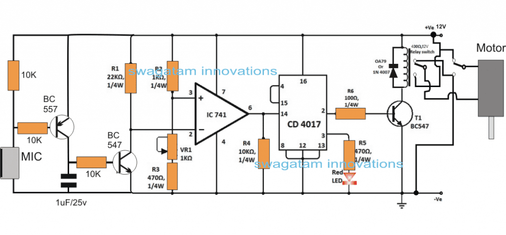 The circuit is made up three basic stages: the MIC amplifier stage, the opamp comparator stage and an IC 4017 based flip flop stage.
The IC 741 is configured as a comparator and together with the IC 4017 it forms a basic clap operated switch circuit.
The BC557/BC547 constitutes the MIC amplifier circuit, we have used two transistors here to make the design highly sensitive to the clap sounds.
Whenever a clap sound or any similar sound is detected by the MIC, it instantly conducts and causes a low signal across its leads enabling the BC557 to trigger.
BC557 triggering forces the BC547 to conduct even harder and in the course brings the pin#2 of IC 741 to ground level or lower than the pin#3 reference pin of the IC.
This action enables the opamp output to go high causing a positive trigger for the 4017 input pin#14.
The above functioning forces the IC 4017 to change states across its output pins #2 and pin#3 alternately with every clap sound detection.
The output from the IC 4017 can be seen connected with a relay driver stage consisting of a DPDT relay with its dual contacts configured with the toy car motors, and the supply rails.
The flip flop action from the IC 4017 output toggles the relay contacts across their N/C and N/O points, thereby causing the car motor to correspondingly rotate in cock-wise and anticlockwise directions in response to the subsequent clap sounds, and thus the car is able to move forward or backward accordingly.
In order to make this clap operated toy circuit make sure to wire the indicated relay contacts across both the motors of the car which may be attached at the front of the rear sides of the unit, and must have a gear box configured with the wheels.
The circuit is made up three basic stages: the MIC amplifier stage, the opamp comparator stage and an IC 4017 based flip flop stage.
The IC 741 is configured as a comparator and together with the IC 4017 it forms a basic clap operated switch circuit.
The BC557/BC547 constitutes the MIC amplifier circuit, we have used two transistors here to make the design highly sensitive to the clap sounds.
Whenever a clap sound or any similar sound is detected by the MIC, it instantly conducts and causes a low signal across its leads enabling the BC557 to trigger.
BC557 triggering forces the BC547 to conduct even harder and in the course brings the pin#2 of IC 741 to ground level or lower than the pin#3 reference pin of the IC.
This action enables the opamp output to go high causing a positive trigger for the 4017 input pin#14.
The above functioning forces the IC 4017 to change states across its output pins #2 and pin#3 alternately with every clap sound detection.
The output from the IC 4017 can be seen connected with a relay driver stage consisting of a DPDT relay with its dual contacts configured with the toy car motors, and the supply rails.
The flip flop action from the IC 4017 output toggles the relay contacts across their N/C and N/O points, thereby causing the car motor to correspondingly rotate in cock-wise and anticlockwise directions in response to the subsequent clap sounds, and thus the car is able to move forward or backward accordingly.
In order to make this clap operated toy circuit make sure to wire the indicated relay contacts across both the motors of the car which may be attached at the front of the rear sides of the unit, and must have a gear box configured with the wheels.

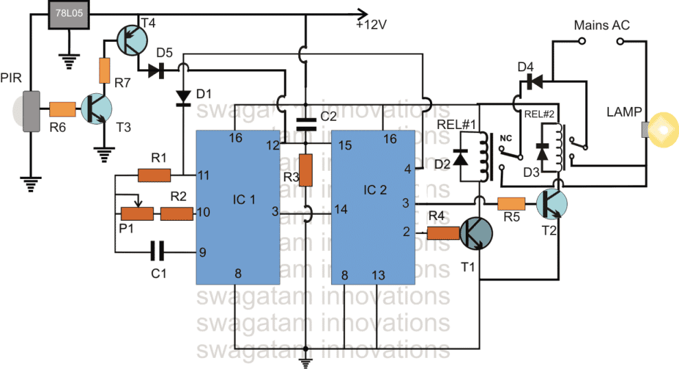 Parts List
R1 = 2M2
R2,R4.R5,R6,R7= 10K
R3= 100
P1 = 1M
C1 = 1uF/25V
C2=0.22uF
T1,T2,T3 = BC547
T4 = BC557
D1,D5 = 1N4148
D4= 6A4
D2,D3 = 1N4007
IC1 = 4060
IC2 = 4017
Parts List
R1 = 2M2
R2,R4.R5,R6,R7= 10K
R3= 100
P1 = 1M
C1 = 1uF/25V
C2=0.22uF
T1,T2,T3 = BC547
T4 = BC557
D1,D5 = 1N4148
D4= 6A4
D2,D3 = 1N4007
IC1 = 4060
IC2 = 4017
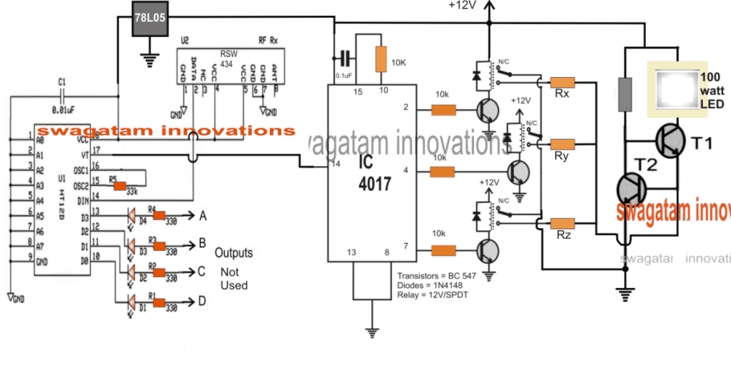
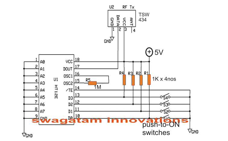
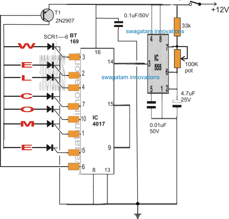
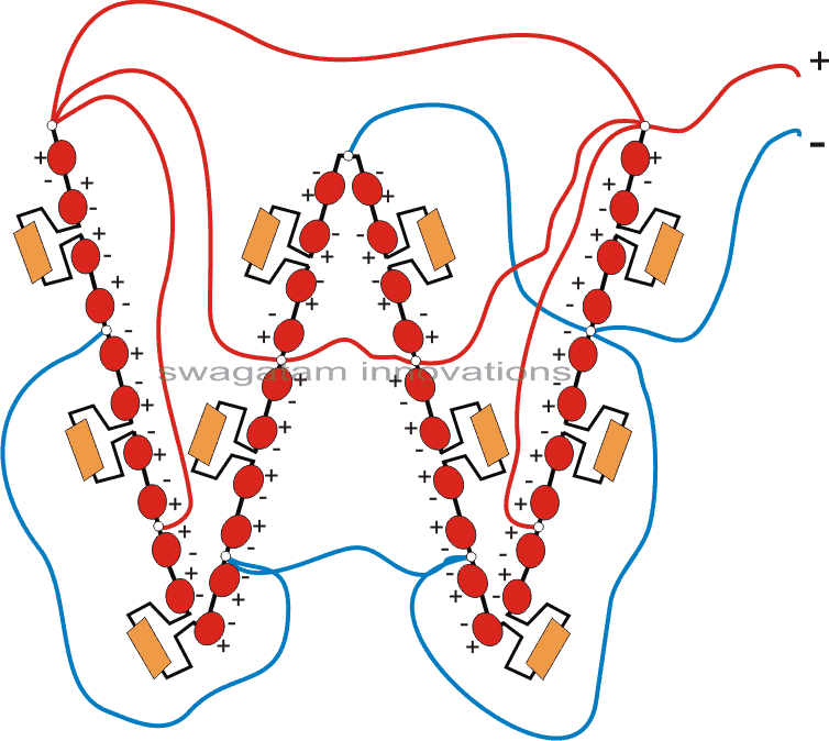 In the same way other alphabets could be easily configured and wired together for developing the required "welcome" chasing LED display circuit.
The series resistors across each of the 4 series LED string can be calculated using the linked software.
All LEDs are red LEDs/5mm/20mA/High Bright
For 4 LED series the resistor value will be = 25 Ohms 1/4 watt
If there are 3 LED series the resistor value will be = 175 Ohms 1/4 watt
If there are 2 LED series the resistor value will be = 330 Ohms 1/4 watt
In the same way other alphabets could be easily configured and wired together for developing the required "welcome" chasing LED display circuit.
The series resistors across each of the 4 series LED string can be calculated using the linked software.
All LEDs are red LEDs/5mm/20mA/High Bright
For 4 LED series the resistor value will be = 25 Ohms 1/4 watt
If there are 3 LED series the resistor value will be = 175 Ohms 1/4 watt
If there are 2 LED series the resistor value will be = 330 Ohms 1/4 watt
 We can clearly see that the multilevel 5 step cascaded concept produces a more obvious and effective simulation of a real sine wave than the SPWM concept which relies solely on matching the RMS value with the original sine wave magnitude.
Designing a conventional 5 Level Cascaded sine wave Inverter can be quite complex, but the concept which is explained here makes the implementation easier and employs ordinary components.
We can clearly see that the multilevel 5 step cascaded concept produces a more obvious and effective simulation of a real sine wave than the SPWM concept which relies solely on matching the RMS value with the original sine wave magnitude.
Designing a conventional 5 Level Cascaded sine wave Inverter can be quite complex, but the concept which is explained here makes the implementation easier and employs ordinary components.
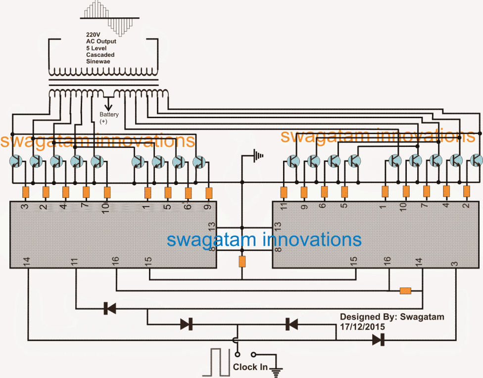 NOTE: Please add a 1uF/25 capacitor across pin#15 and pin#16 lines of the ICs, otherwise the sequencing will not initiate.
Referring to the image above, we can see how simply the 5 level cascaded inverter concept can be practically implemented using just a muti-tap transformer, a couple of 4017 ICs and 18 power BJTs, which could be easily replaced with mosfets if required.
Here a couple of 4017 ICs which are Johnson's 10 stage counter divider chips, are cascaded to produce a sequentially running or chasing logic highs across the shown pinouts of the ICs.
NOTE: Please add a 1uF/25 capacitor across pin#15 and pin#16 lines of the ICs, otherwise the sequencing will not initiate.
Referring to the image above, we can see how simply the 5 level cascaded inverter concept can be practically implemented using just a muti-tap transformer, a couple of 4017 ICs and 18 power BJTs, which could be easily replaced with mosfets if required.
Here a couple of 4017 ICs which are Johnson's 10 stage counter divider chips, are cascaded to produce a sequentially running or chasing logic highs across the shown pinouts of the ICs.
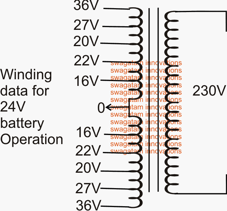 As may be witnessed in the above diagram, the transformer is an ordinary iron core type, made by winding the primary and the secondary with turns corresponding to the indicated voltage taps.
When connected with the corresponding BJTs these winding can be expected to induce a 5 level or a total of 9 level of cascaded waveform wherein the first 36V winding would correspond and induce a 150V, the 27V would induce an equivalent of 200V, while the 20V, 27V, 36V would be responsible of producing 230V, 270V and 330V across the secondary winding in the proposed cascaded format.
The set of taps on the lower side of the primary would carry out the switching to complete 4 ascending levels of the waveform.
An identical procedure would be repeated by the 9 BJTs associated with the complementary 4017 IC for building the negative half cycle of the AC...the negative is rendered due to the opposite orientation of the transformer winding with respect to the center tap.
Update:
Complete circuit diagram of the discussed multi-level sinewave inverter circuit
As may be witnessed in the above diagram, the transformer is an ordinary iron core type, made by winding the primary and the secondary with turns corresponding to the indicated voltage taps.
When connected with the corresponding BJTs these winding can be expected to induce a 5 level or a total of 9 level of cascaded waveform wherein the first 36V winding would correspond and induce a 150V, the 27V would induce an equivalent of 200V, while the 20V, 27V, 36V would be responsible of producing 230V, 270V and 330V across the secondary winding in the proposed cascaded format.
The set of taps on the lower side of the primary would carry out the switching to complete 4 ascending levels of the waveform.
An identical procedure would be repeated by the 9 BJTs associated with the complementary 4017 IC for building the negative half cycle of the AC...the negative is rendered due to the opposite orientation of the transformer winding with respect to the center tap.
Update:
Complete circuit diagram of the discussed multi-level sinewave inverter circuit
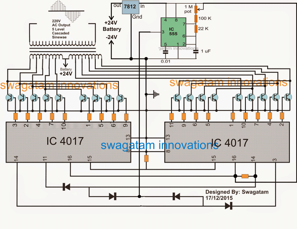 NOTE: Please add a 1uF/25 capacitor across pin#15 and pin#16 lines of the ICs, otherwise the sequencing will not initiate.
The 1M pot associated with the 555 circuit will need to be adjusted for setting up a 50Hz or a 60Hz frequency for the inverter as per the country specs of the user.
NOTE: Please add a 1uF/25 capacitor across pin#15 and pin#16 lines of the ICs, otherwise the sequencing will not initiate.
The 1M pot associated with the 555 circuit will need to be adjusted for setting up a 50Hz or a 60Hz frequency for the inverter as per the country specs of the user.
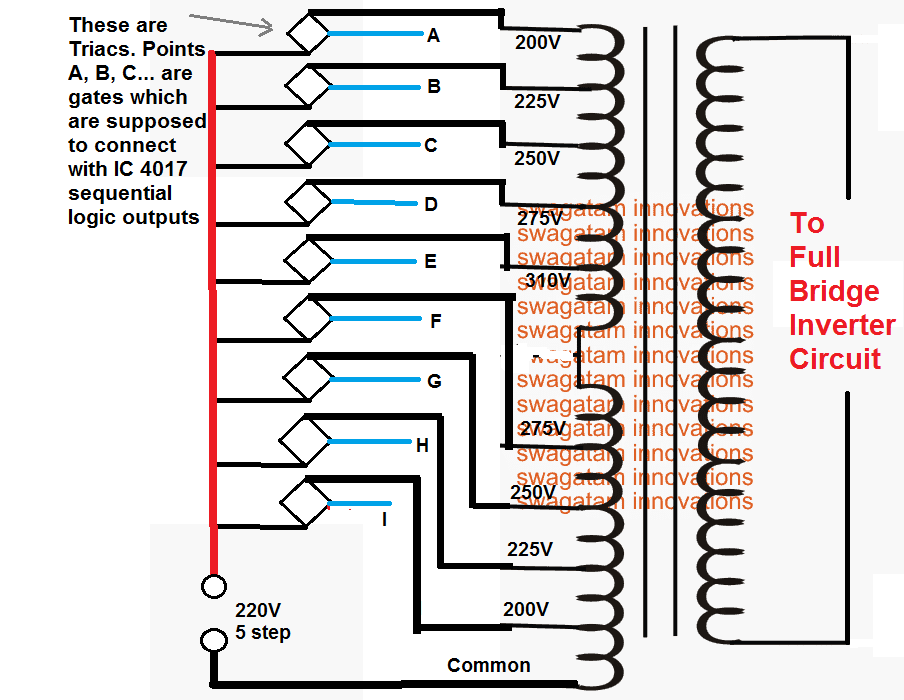

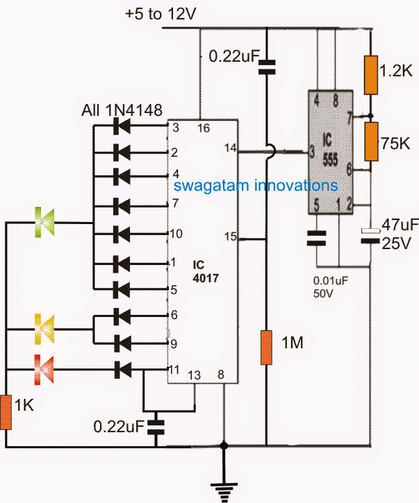
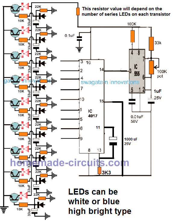 Parts List
All resistors are 1/4 watt 5%
10K - 9
22k - 9
33k - 1
100k pot - 1
3k3 - 1
1N4148 - 9
IC 4017 - 1
IC 555 - 1
BC547 - 9
LEDs Blue/RED - 9 to 36 (1 to 4 in series on each channel)
33uF/25 - 9
1uF/25V - 1
1000uF/25 - 1
0.1uF - 1
Note: The 100K on IC 555 pin#4 can be removed and pin#4 connected directly to the positive line.
The 1000uF can be reduced, if the 3k3 is increased proportionately.
Video Demonstration
PLEASE IGNORE THE DESIGN DISCUSSED IN THE FOLLOWING SECTIONS BECAUSE IT IS AN OLDER DESIGN AND HAS NOT BEEN VERIFIED THROUGH PRACTICAL TESTING.
Parts List
All resistors are 1/4 watt 5%
10K - 9
22k - 9
33k - 1
100k pot - 1
3k3 - 1
1N4148 - 9
IC 4017 - 1
IC 555 - 1
BC547 - 9
LEDs Blue/RED - 9 to 36 (1 to 4 in series on each channel)
33uF/25 - 9
1uF/25V - 1
1000uF/25 - 1
0.1uF - 1
Note: The 100K on IC 555 pin#4 can be removed and pin#4 connected directly to the positive line.
The 1000uF can be reduced, if the 3k3 is increased proportionately.
Video Demonstration
PLEASE IGNORE THE DESIGN DISCUSSED IN THE FOLLOWING SECTIONS BECAUSE IT IS AN OLDER DESIGN AND HAS NOT BEEN VERIFIED THROUGH PRACTICAL TESTING.
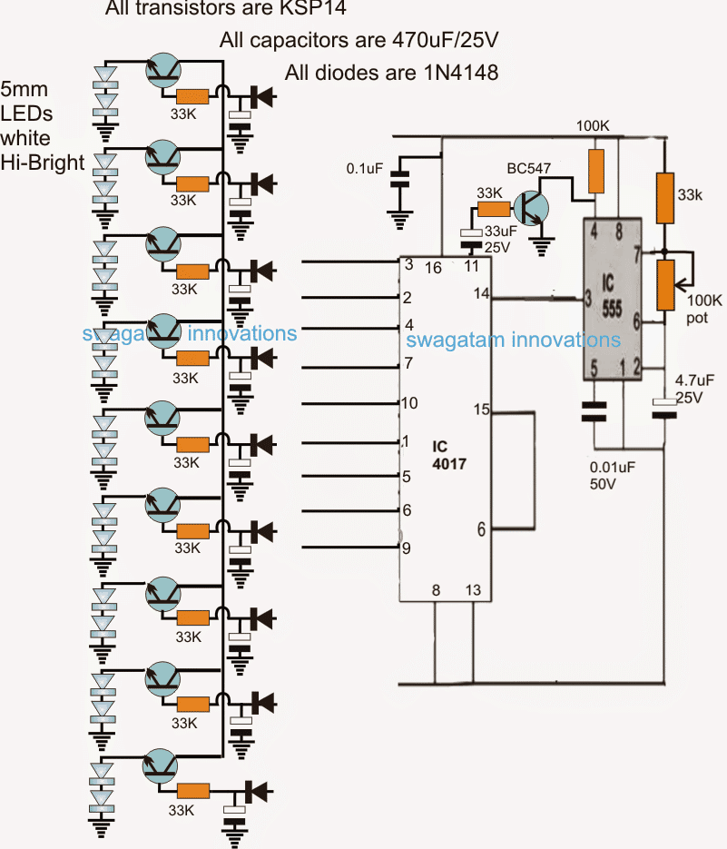 The idea could be achieved through the circuit represented above, using a Johnson's decade counter and a 555 astable clock generator circuit.
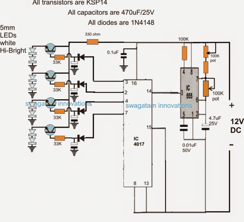
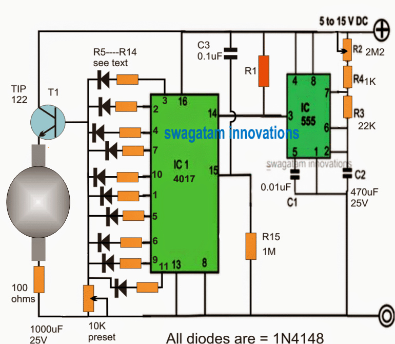
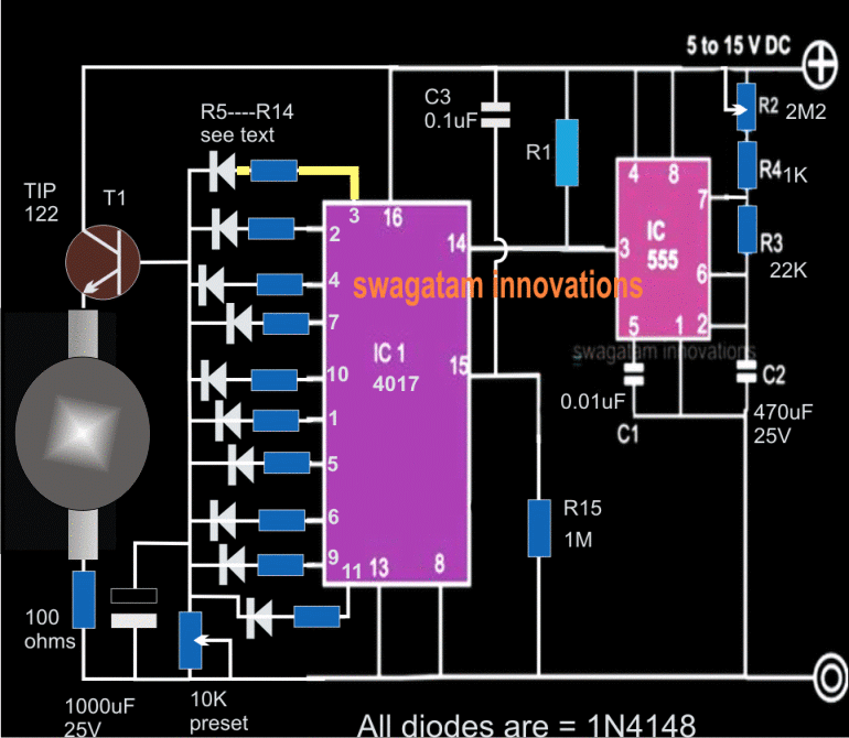 An easier and cheaper alternative for a revolving LED beacon light can be seen below, although the effect may not be as impressive as the above design.
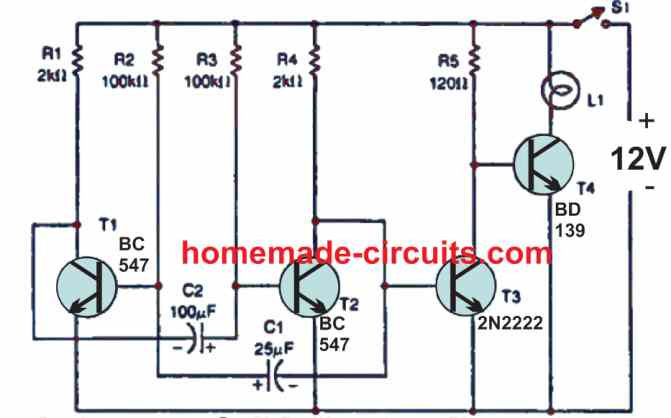
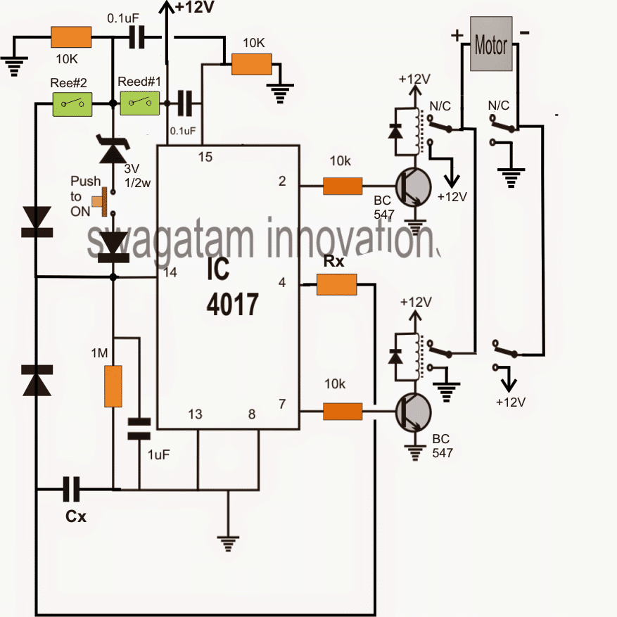
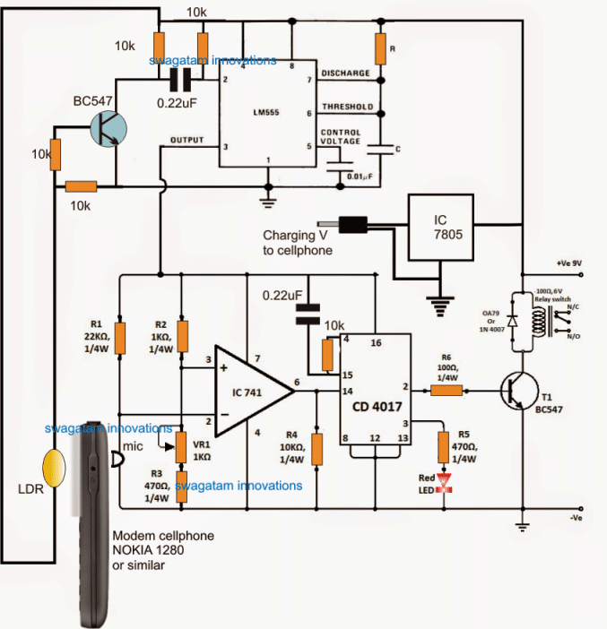 The lower section of the circuit incorporating the IC 741 and the IC 4017 forms a simple sound activated relay circuit, which toggles the connected relay alternately ON and OFF in response to the sound signals received on the MIC.
Basically this circuit is used in clap switch circuits for toggling the relay with clap sounds.
For the proposed application the sound is produced from the cellphone when the user calls the shown attached cellphone from his home or some distant location for operating the relay and the water pump.
The idea looks pretty simple until here, however the mic could be triggered even with a false sound trigger generated externally in the filed, for example by an airplane sound flying close by or a vehicle such as a tractor engine sound etc.
The lower section of the circuit incorporating the IC 741 and the IC 4017 forms a simple sound activated relay circuit, which toggles the connected relay alternately ON and OFF in response to the sound signals received on the MIC.
Basically this circuit is used in clap switch circuits for toggling the relay with clap sounds.
For the proposed application the sound is produced from the cellphone when the user calls the shown attached cellphone from his home or some distant location for operating the relay and the water pump.
The idea looks pretty simple until here, however the mic could be triggered even with a false sound trigger generated externally in the filed, for example by an airplane sound flying close by or a vehicle such as a tractor engine sound etc.
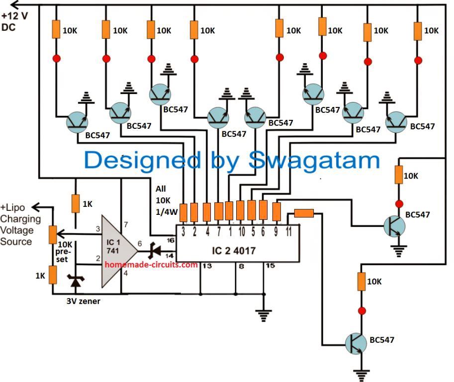 The second diagram below is the relay driver stage which needs to be repeated 10 times and the base of the BC557 associated with the red spots of the relevant BC547 stages from the first circuit below.
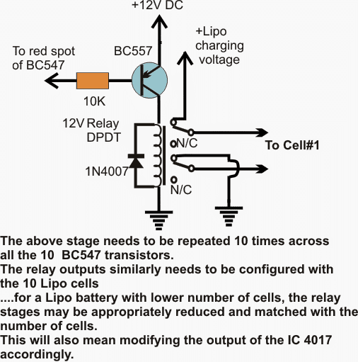 If the cells are 3.7V rated, the opamp preset is adjusted such that its output pin#6 just goes high when the charge level across the cell reaches around 4.2V.
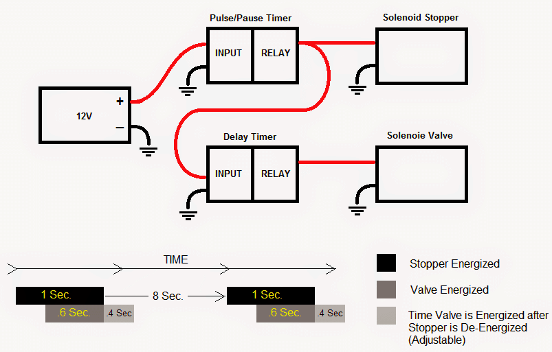
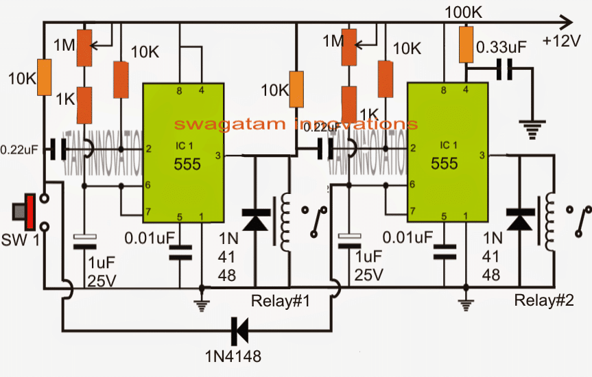 The circuit is designed such that it includes both the timer stages (t1 and t2) together, and the external pause/pulse mechanism can be eliminated.
Basically two IC 555 stages are used here which are coupled together in series, both of these are configured as monostable operators.
When power is switched ON, the pin#3 of the left IC is held at a low logic which triggers pin#2 of the right hand side IC to ground, however pin#3 of the right side IC is unable to go high and respond to this trigger because its pin#4 simultaneously goes through a momentary disabling (resetting) via the 100k and the 0.33uF capacitor.
Thus in the meantime its pin#2 capacitor 0.22uF charges and keeps things frozen for the moment with no reaction on the connected relay.
SW1 forms the trigger initiator, as soon as SW1 is pushed, pin#2 of the left IC receives a ground signal and pulls pin#3 of the IC high, activating relay#1....the solenoid stopper now gets energized through this relay.
The above action allows the right side IC pin#2 capacitor to get discharged via the two 10K resistors across its ends and allows this IC to attain a standby position.
The left side IC now counts depending upon the setting of its 1M preset and the 1uF/25V capacitor.
Once the time elapses, pin#3 of the left IC reverts to logic zero, causing a momentary negative pulse to pin#2 of the right side IC.
Relay#1 deactivates, de-energizing the stopper solenoid connected to it.
This prompts a sequential toggling of the right side relay whose pin#3 now becomes high and which in turn switches ON the connected relay#2. The solenoid valve instantly get energized at this instance via relay#2.
The IC now begins counting the delay period as set by the RC components across its pin#6/2.
Once the timing of the right side IC too elapses, its pin#3 goes low deactivating relay#2, and resetting the timers to its original condition.
The diode linking the two ICs makes sure that while the right IC is counting, any triggering of SW1 only helps to prolong the counting of the IC due to the resetting (discharging) of its timing capacitor at pin6/2.
The circuit is designed such that it includes both the timer stages (t1 and t2) together, and the external pause/pulse mechanism can be eliminated.
Basically two IC 555 stages are used here which are coupled together in series, both of these are configured as monostable operators.
When power is switched ON, the pin#3 of the left IC is held at a low logic which triggers pin#2 of the right hand side IC to ground, however pin#3 of the right side IC is unable to go high and respond to this trigger because its pin#4 simultaneously goes through a momentary disabling (resetting) via the 100k and the 0.33uF capacitor.
Thus in the meantime its pin#2 capacitor 0.22uF charges and keeps things frozen for the moment with no reaction on the connected relay.
SW1 forms the trigger initiator, as soon as SW1 is pushed, pin#2 of the left IC receives a ground signal and pulls pin#3 of the IC high, activating relay#1....the solenoid stopper now gets energized through this relay.
The above action allows the right side IC pin#2 capacitor to get discharged via the two 10K resistors across its ends and allows this IC to attain a standby position.
The left side IC now counts depending upon the setting of its 1M preset and the 1uF/25V capacitor.
Once the time elapses, pin#3 of the left IC reverts to logic zero, causing a momentary negative pulse to pin#2 of the right side IC.
Relay#1 deactivates, de-energizing the stopper solenoid connected to it.
This prompts a sequential toggling of the right side relay whose pin#3 now becomes high and which in turn switches ON the connected relay#2. The solenoid valve instantly get energized at this instance via relay#2.
The IC now begins counting the delay period as set by the RC components across its pin#6/2.
Once the timing of the right side IC too elapses, its pin#3 goes low deactivating relay#2, and resetting the timers to its original condition.
The diode linking the two ICs makes sure that while the right IC is counting, any triggering of SW1 only helps to prolong the counting of the IC due to the resetting (discharging) of its timing capacitor at pin6/2.
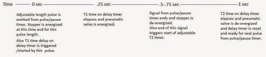 As per the above discussion I have made the appropriate changes in the design, the finalized layout may be witnessed below, and understood with the adjoining explanation:
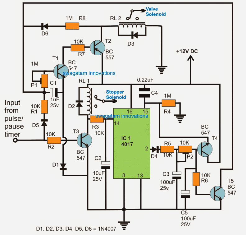 Positive supply is applied to the pin#16 rail of the IC 4017, when switched ON, C4 resets the IC causing pin#2 to produce a zero logic at the base of T3, and the entire circuit waits in a standby condition.
When a positive pulse is applied to the base of T2 from the external pulse/pause timer, T3 instantly conducts and actuates RL1 switching ON the "stopper solenoid".
In the meantime C1/P1 along with T1/T2 which forms a short delay ON timer circuit (t1) also responds to the external trigger and latches via R8/D6 and in the process activates RL2 after some delay as determined by the setting of P1/C1.
RL2 now actuates the pneumatic valve.
After a predetermined delay, the pause pulse timer switches OFF, turning OFF T3 and RL1 along with the stopper solenoid.
As soon as T3 switches OFF, pin14 of the IC4017 receives a positive trigger pulse via the relay coil and R3.
The above trigger forces a sequential high logic to jump from pin#3 (not shown) to pin#2 of the IC.
Another "delay ON timer" (t2) connected across pin#2 of the IC now begins counting, and after some delay T4 is switched ON, along with T5.
T4 sends a resetting pulse to pin#15 of the IC, while T5 conducts and makes sure that the T1/T2 latch breaks so that RL2 is deactivated along with the valve solenoid.
The above actions completely resets the entire circuit until the next input from the pulse/pause timer is applied.
Positive supply is applied to the pin#16 rail of the IC 4017, when switched ON, C4 resets the IC causing pin#2 to produce a zero logic at the base of T3, and the entire circuit waits in a standby condition.
When a positive pulse is applied to the base of T2 from the external pulse/pause timer, T3 instantly conducts and actuates RL1 switching ON the "stopper solenoid".
In the meantime C1/P1 along with T1/T2 which forms a short delay ON timer circuit (t1) also responds to the external trigger and latches via R8/D6 and in the process activates RL2 after some delay as determined by the setting of P1/C1.
RL2 now actuates the pneumatic valve.
After a predetermined delay, the pause pulse timer switches OFF, turning OFF T3 and RL1 along with the stopper solenoid.
As soon as T3 switches OFF, pin14 of the IC4017 receives a positive trigger pulse via the relay coil and R3.
The above trigger forces a sequential high logic to jump from pin#3 (not shown) to pin#2 of the IC.
Another "delay ON timer" (t2) connected across pin#2 of the IC now begins counting, and after some delay T4 is switched ON, along with T5.
T4 sends a resetting pulse to pin#15 of the IC, while T5 conducts and makes sure that the T1/T2 latch breaks so that RL2 is deactivated along with the valve solenoid.
The above actions completely resets the entire circuit until the next input from the pulse/pause timer is applied.

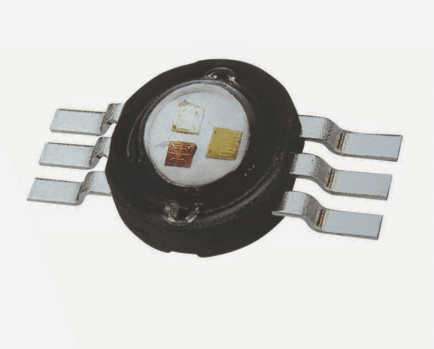 We'll require 24 of these LEDs for producing intended scrolling effect, once procured these may be assembled serially as shown in the following image:
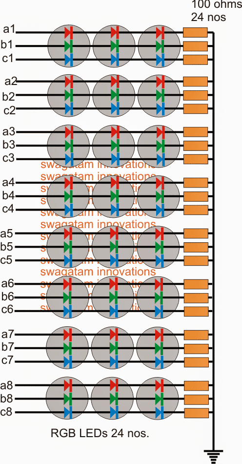 As can be seen , the cathodes are all made common and grounded via individual 100 ohm resistors (connected to the negative supply f the circuit).
The anode ends can be seen designated with some relevant numbers which need to be appropriately connected with the respective output pinouts of the IC 4017 circuit as shown in the following figure:
As can be seen , the cathodes are all made common and grounded via individual 100 ohm resistors (connected to the negative supply f the circuit).
The anode ends can be seen designated with some relevant numbers which need to be appropriately connected with the respective output pinouts of the IC 4017 circuit as shown in the following figure:
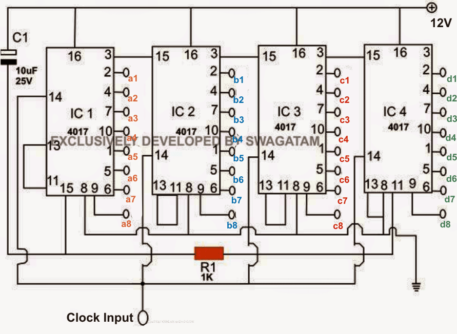
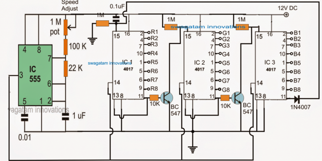 We learned and understood how exactly the above RGB controller circuit is supposed to function with the stipulated sequencing procedures, now it would be interesting to see how the sequencing outputs from the above circuit may be used with a compatible driver stage for producing the scrolling or moving RGB LED over a selected set of alphabets.
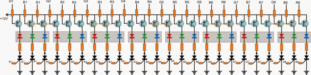 All transistors are 2N2907
All SCRs are BT169
SCR gate resistors and PNP base resistors are all 1K
LED series resistors will be as per the LED current.
The above image depicts the RGB driver stage, we can see 8 numbers of RGB LEDs utilized (in the shaded square boxes), this is because the discussed 4017 Circuit is designed to produce 8 sequential outputs and therefore the driver stage too accommodated 8 numbers of these LEDs.
To learn more about RGB LEDs you can refer to the following related posts:
RGB color mixer circuit
RGB flasher, controller circuit
All transistors are 2N2907
All SCRs are BT169
SCR gate resistors and PNP base resistors are all 1K
LED series resistors will be as per the LED current.
The above image depicts the RGB driver stage, we can see 8 numbers of RGB LEDs utilized (in the shaded square boxes), this is because the discussed 4017 Circuit is designed to produce 8 sequential outputs and therefore the driver stage too accommodated 8 numbers of these LEDs.
To learn more about RGB LEDs you can refer to the following related posts:
RGB color mixer circuit
RGB flasher, controller circuit
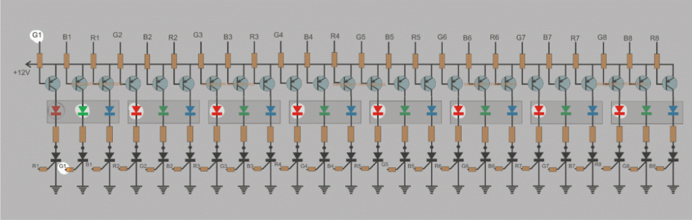 The above shown animated simulation provides an exact replica of the scrolling of the LEDs that may be expected from the proposed design.
The indicated running white spots on the SCR gates indicate the triggering and the execution of the latching function by the SCRs, while the PNP base white spots indicate the breaking of the relevant SCR latches.
Single LEDs are shown in the sequence, but depending on the supply voltage more numbers of series LEDs could be inserted within each of the RGB channels.
For example with a 12V supply 3 LEDs may be incorporated on each of the channels, with 24V this may be increased to 6 LEDs on each of the channels.
The above shown animated simulation provides an exact replica of the scrolling of the LEDs that may be expected from the proposed design.
The indicated running white spots on the SCR gates indicate the triggering and the execution of the latching function by the SCRs, while the PNP base white spots indicate the breaking of the relevant SCR latches.
Single LEDs are shown in the sequence, but depending on the supply voltage more numbers of series LEDs could be inserted within each of the RGB channels.
For example with a 12V supply 3 LEDs may be incorporated on each of the channels, with 24V this may be increased to 6 LEDs on each of the channels.
 The above example shows a classic RGB moving graphical alphabet simulation using the above explained circuit.
Each alphabet can be seen wired with the red, green and the blue LEDs from the 8 RGB LED modules.
The series parallel connections can be a little complex, and might require some experience and skill, the following articles can be studied for understanding the calculations involved for wiring LEDs in series and parallel:
How to Wire LED Lights
The above example shows a classic RGB moving graphical alphabet simulation using the above explained circuit.
Each alphabet can be seen wired with the red, green and the blue LEDs from the 8 RGB LED modules.
The series parallel connections can be a little complex, and might require some experience and skill, the following articles can be studied for understanding the calculations involved for wiring LEDs in series and parallel:
How to Wire LED Lights
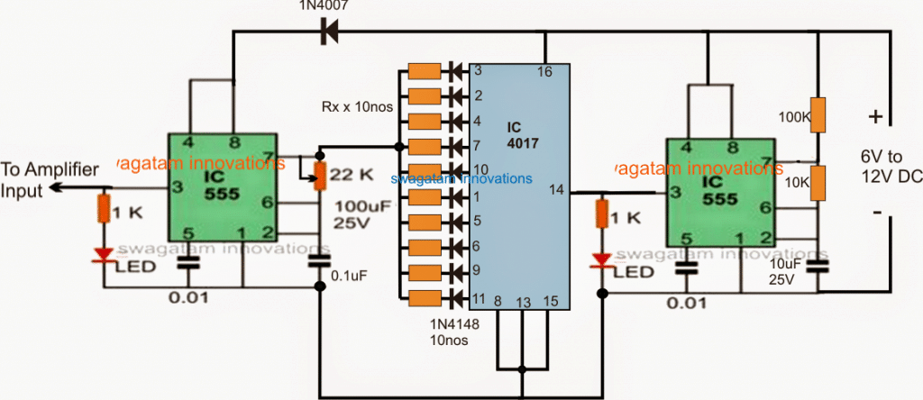 Referring to the above diagram, the design depicts an ultrasonic frequency generator circuit which features a random frequency selector stage.
The idea may be understood with the help of the following explanation:
The IC 555 stages on the left and on the right side are both configured as astable multivibrators for generating the respective frequencies across their output pin#3.
Referring to the above diagram, the design depicts an ultrasonic frequency generator circuit which features a random frequency selector stage.
The idea may be understood with the help of the following explanation:
The IC 555 stages on the left and on the right side are both configured as astable multivibrators for generating the respective frequencies across their output pin#3.

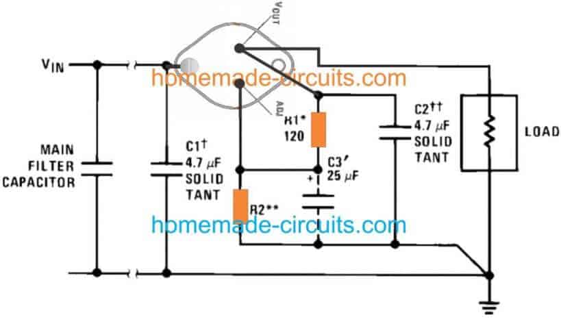
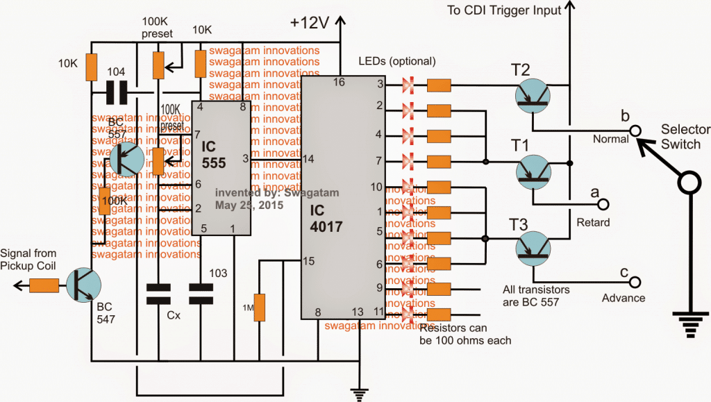
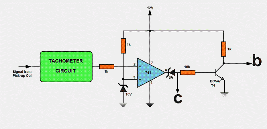
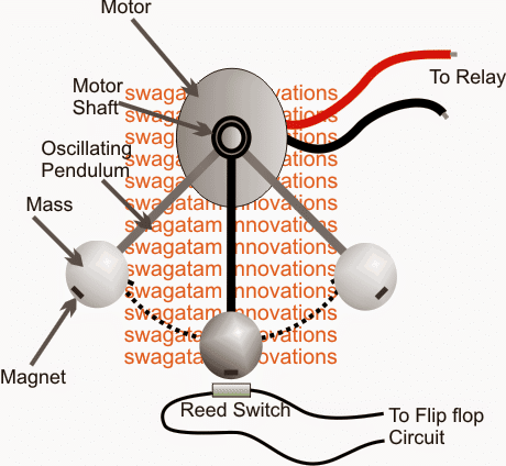
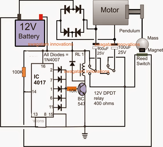

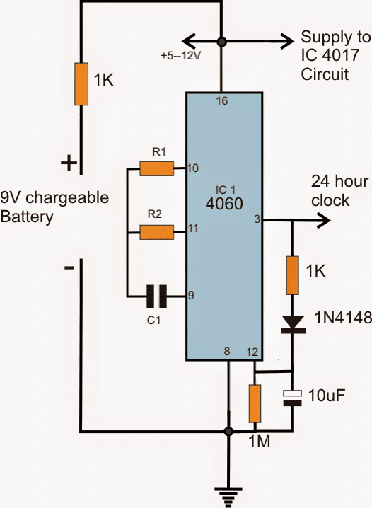
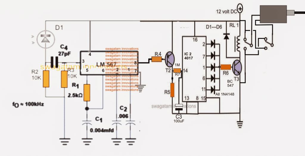
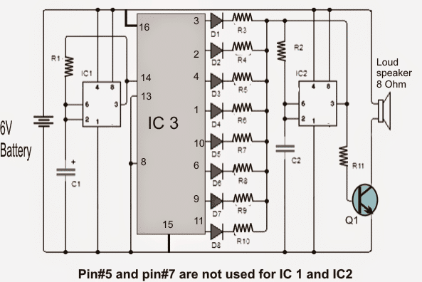
 This is the photo of circuit i got from internet.
but am not able to understand how to make it help please.
please suggest a simple circuit using easily available components.
for RGB controller.
The sequence pattern will be: red first, then green, then blue, then red green together.
or any order and any combination will do.
i just need it for making a led display board.
only wish is that leds should light in sequence and combinations.
This is the photo of circuit i got from internet.
but am not able to understand how to make it help please.
please suggest a simple circuit using easily available components.
for RGB controller.
The sequence pattern will be: red first, then green, then blue, then red green together.
or any order and any combination will do.
i just need it for making a led display board.
only wish is that leds should light in sequence and combinations.
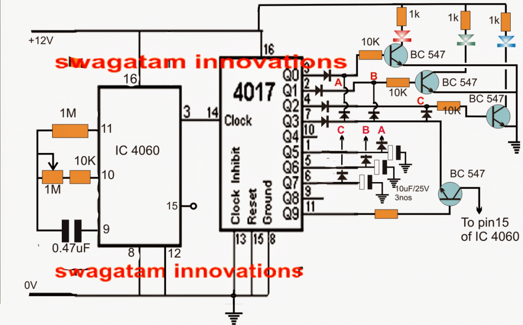
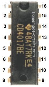 Parts list for the morse code lamp for lighthouse application
R1 = TO BE CALCULATED
R2, R3, R4, R6, R7 = 1M
R5 = 1K
P1 = 100K PRESET
C1, C2, C3 = 0.22uF
C4 = 10uF/25V
D1---D8 = 1N4148
T1 = 2N2222
T2 = BC557
IC1 = 4060
IC2 = 4017
Parts list for the morse code lamp for lighthouse application
R1 = TO BE CALCULATED
R2, R3, R4, R6, R7 = 1M
R5 = 1K
P1 = 100K PRESET
C1, C2, C3 = 0.22uF
C4 = 10uF/25V
D1---D8 = 1N4148
T1 = 2N2222
T2 = BC557
IC1 = 4060
IC2 = 4017
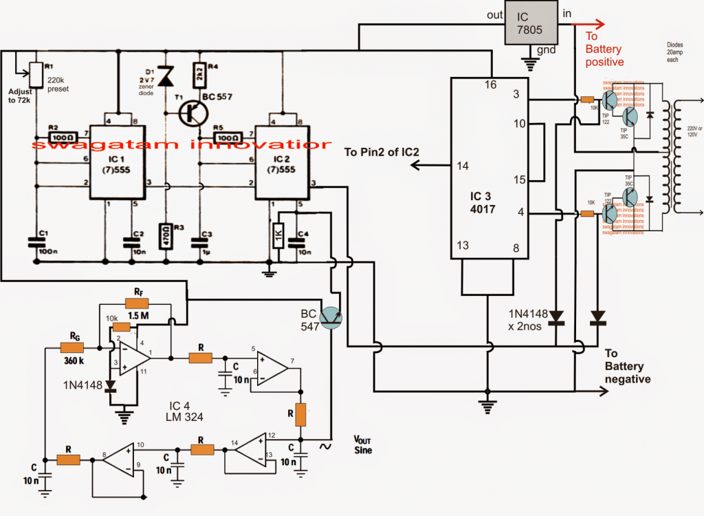 NOTE: Please use a Darlingtton pair for the BC547 connected with pin#5 of IC2 for efficient PWM conversion.
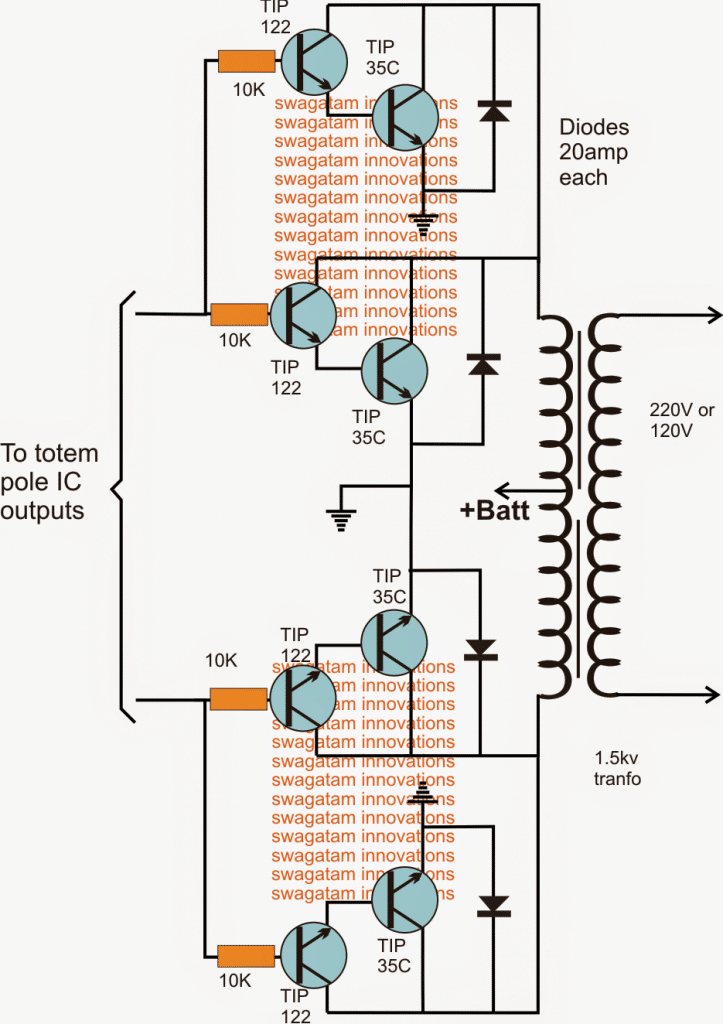
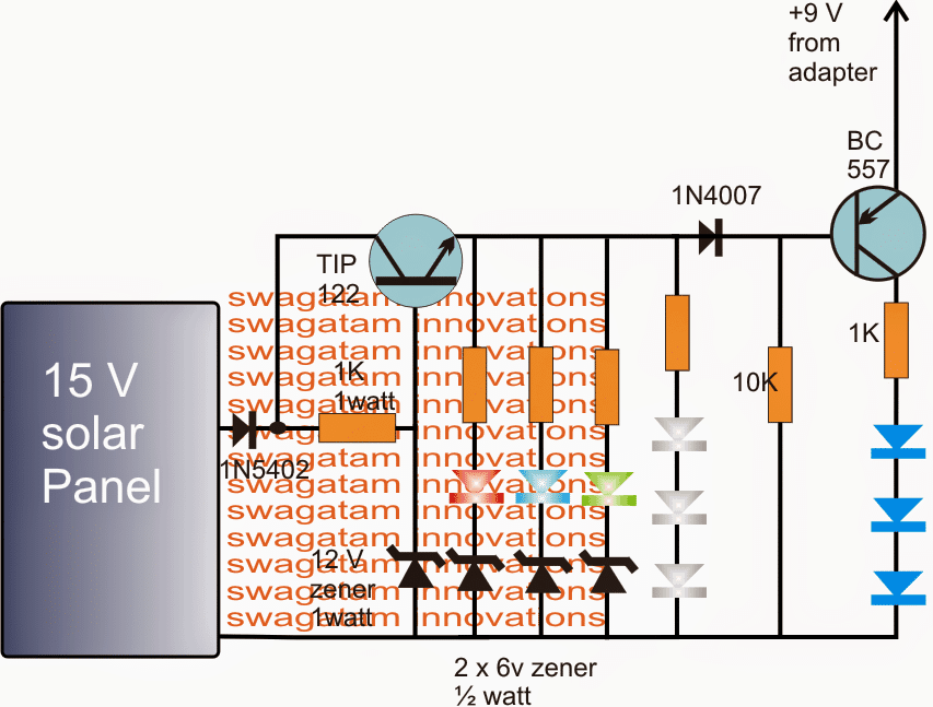
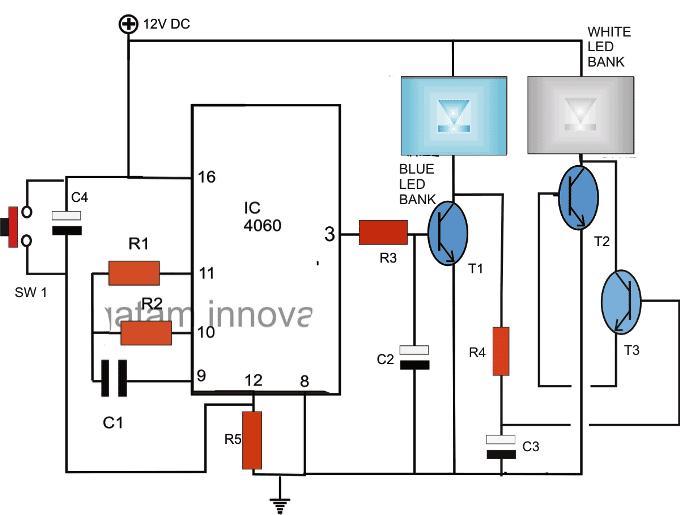
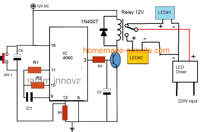
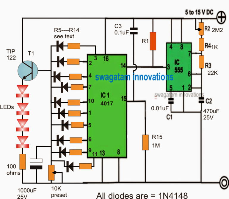
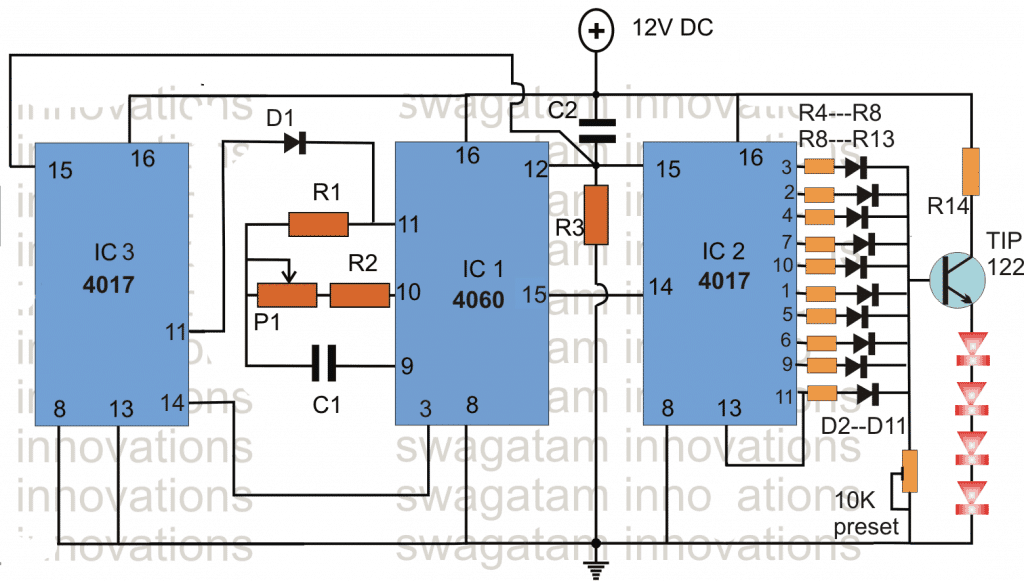 Here the IC 4060 is used as a timer oscillator whose pin#15 is used for generating a relatively faster frequency for the IC2, such that the outputs of IC2 are able to genearte the required slow glow and slow fade sequencing effect on the LED driver transistor within 12 hour period.
On the other hand pin#3 of the IC 4060 which geneartes around 7 to 8 times slower frequency than pin #15 clocks IC3 appropriately, and this inclusion becomes responsible for the 24 hour resetting feature in this new circuit.
Pin#15 and pin#3 are arbritarily chosen here with an assumption that pin#15 would enable the LEDs to operate for 12 hours, while pin#3 pulse rate will reset the IC1 after every 24 hours via IC3.
This timing will need to be tested with some trial and error using the available extensive range option that IC1 and IC3 are able to provide through their 10nos of output pins, and these may be experimented for getting the most favarable timing range across both the features, that is for 12 hour LED effect and for the 24 hour reset.
Also do not forget the P1 adjustment which further adds to the adjustment range of the design.
Here the IC 4060 is used as a timer oscillator whose pin#15 is used for generating a relatively faster frequency for the IC2, such that the outputs of IC2 are able to genearte the required slow glow and slow fade sequencing effect on the LED driver transistor within 12 hour period.
On the other hand pin#3 of the IC 4060 which geneartes around 7 to 8 times slower frequency than pin #15 clocks IC3 appropriately, and this inclusion becomes responsible for the 24 hour resetting feature in this new circuit.
Pin#15 and pin#3 are arbritarily chosen here with an assumption that pin#15 would enable the LEDs to operate for 12 hours, while pin#3 pulse rate will reset the IC1 after every 24 hours via IC3.
This timing will need to be tested with some trial and error using the available extensive range option that IC1 and IC3 are able to provide through their 10nos of output pins, and these may be experimented for getting the most favarable timing range across both the features, that is for 12 hour LED effect and for the 24 hour reset.
Also do not forget the P1 adjustment which further adds to the adjustment range of the design.
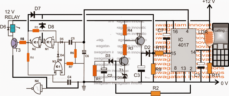
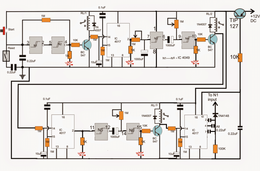 Referring to proposed tank fill/drain sequence controller circuit diagram, when power is first applied at the emitter of the PNP 2N2907, its base capacitor momentarily allows it to conduct until pin10 of the bottom-right 4017 latches the base of the transistor into a permanent conduction mode.
The circuit now gets latched and powered.
All the 0.1uF capacitors connected with the pin14 of the 4017 make sure the IC gets reset and in a standby position with their relevant outputs held at a "0" logic.
This ensures that all the relays stay in a deactivated position at power switch ON.
Also, the input capacitor of N1 resets N1/N2 into a negative latch so that the output of N2 commences with a logic zero keeping the relay shut off.
Now when the "start" button is pushed, N1 negative latch is reverted to a positive latch creating a positive at the output of N2 which in turn activates RL1, switching ON the motor solenoid inlet valve that may be connected across its N/O contacts and mains.
The inlet valve keeps water running in the tank until it reaches the specified threshold, triggering the reed relay into a closed position.
This action yet again grounds the N1 input via the series capacitor reverting the N1/N2 latch to its original negative state.
The inlet valve here gets shut off.
Shutting off the above relay transistor causes a positive pulse to emerge at pin14 of the attached IC 4017, which responds by shifting its output high logic from its pin3 to pin2, pin2 now becomes high which begins charging the input capacitor of N3 via the 1M setting until after the predetermined delay the capacitor becomes fully charged causing a high logic at the input of N3.
N3 responds by making its output low which in turn forces the input of N4 to become low and its output high....toggling ON the connected relay driver stage.
This initiates the water pump and keeps it switched ON until the input capacitor of N4 charges fully, reverting N4 output to zero and shutting off the motor.
This delay is determined by the 1M pot at the input of N4.
The switching OFF of the above relay transistor causes the next IC 4017 to push its logic high to its pin2 which quite identically initiates the N5/N6 timing sequence switching ON RL3 and its associated drain solenoid but only until the N6 capacitor gets fully charged wherein the relay shuts off after a delay set by the N6 1M pot
The above switching just like in previous stages influences the last IC 4017 which transfers a logic high at its pin2 inducing a momentary high logic at the input of N1, yet again reverting its latch to a positive mode, simulating the pressing of the start switch....the process begins yet again, and repeats for 3 times until a high logic is forwarded to pin10 of the bottom right 4017.
This high logic blocks the PNP 2N2907 conduction breaking the power supply to the circuit via the PNP, instantly switching OFF the whole circuit into a stand still.
The power now needs to be switched OFF and switched ON again in order to restore the circuit in a standby position.
RL1 = Activates water solenoid
RL2 = Starts 220V water pump (2 min ON delay is adjusted by N3 pot, "t" minutes ON is determined by N4 pot)
RL3 = Opens drain solenoid (t1 is set by adjusting N6 pot)
Referring to proposed tank fill/drain sequence controller circuit diagram, when power is first applied at the emitter of the PNP 2N2907, its base capacitor momentarily allows it to conduct until pin10 of the bottom-right 4017 latches the base of the transistor into a permanent conduction mode.
The circuit now gets latched and powered.
All the 0.1uF capacitors connected with the pin14 of the 4017 make sure the IC gets reset and in a standby position with their relevant outputs held at a "0" logic.
This ensures that all the relays stay in a deactivated position at power switch ON.
Also, the input capacitor of N1 resets N1/N2 into a negative latch so that the output of N2 commences with a logic zero keeping the relay shut off.
Now when the "start" button is pushed, N1 negative latch is reverted to a positive latch creating a positive at the output of N2 which in turn activates RL1, switching ON the motor solenoid inlet valve that may be connected across its N/O contacts and mains.
The inlet valve keeps water running in the tank until it reaches the specified threshold, triggering the reed relay into a closed position.
This action yet again grounds the N1 input via the series capacitor reverting the N1/N2 latch to its original negative state.
The inlet valve here gets shut off.
Shutting off the above relay transistor causes a positive pulse to emerge at pin14 of the attached IC 4017, which responds by shifting its output high logic from its pin3 to pin2, pin2 now becomes high which begins charging the input capacitor of N3 via the 1M setting until after the predetermined delay the capacitor becomes fully charged causing a high logic at the input of N3.
N3 responds by making its output low which in turn forces the input of N4 to become low and its output high....toggling ON the connected relay driver stage.
This initiates the water pump and keeps it switched ON until the input capacitor of N4 charges fully, reverting N4 output to zero and shutting off the motor.
This delay is determined by the 1M pot at the input of N4.
The switching OFF of the above relay transistor causes the next IC 4017 to push its logic high to its pin2 which quite identically initiates the N5/N6 timing sequence switching ON RL3 and its associated drain solenoid but only until the N6 capacitor gets fully charged wherein the relay shuts off after a delay set by the N6 1M pot
The above switching just like in previous stages influences the last IC 4017 which transfers a logic high at its pin2 inducing a momentary high logic at the input of N1, yet again reverting its latch to a positive mode, simulating the pressing of the start switch....the process begins yet again, and repeats for 3 times until a high logic is forwarded to pin10 of the bottom right 4017.
This high logic blocks the PNP 2N2907 conduction breaking the power supply to the circuit via the PNP, instantly switching OFF the whole circuit into a stand still.
The power now needs to be switched OFF and switched ON again in order to restore the circuit in a standby position.
RL1 = Activates water solenoid
RL2 = Starts 220V water pump (2 min ON delay is adjusted by N3 pot, "t" minutes ON is determined by N4 pot)
RL3 = Opens drain solenoid (t1 is set by adjusting N6 pot)
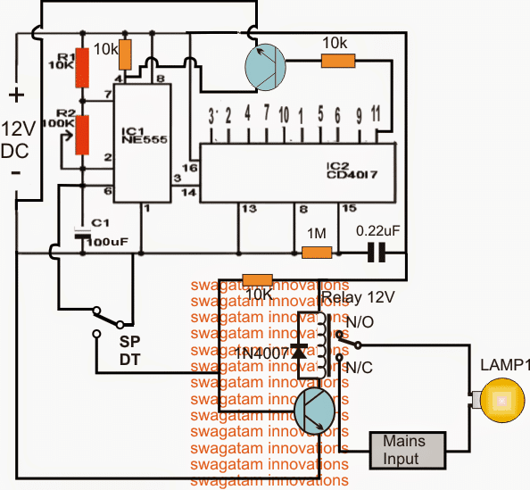
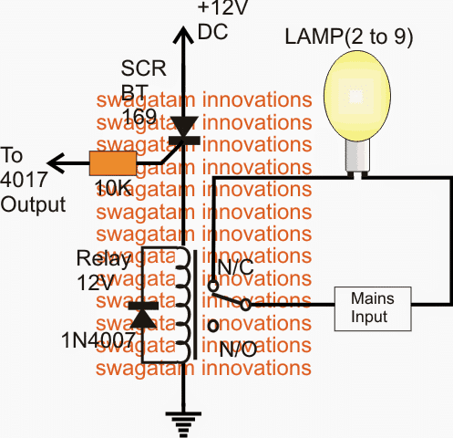
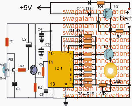

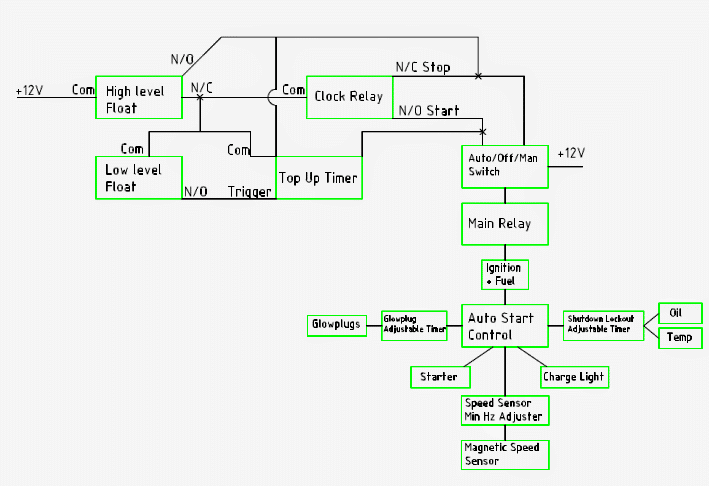 The
The
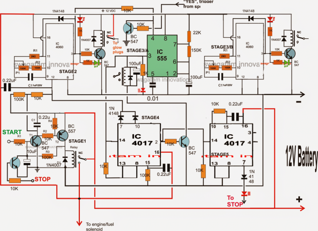
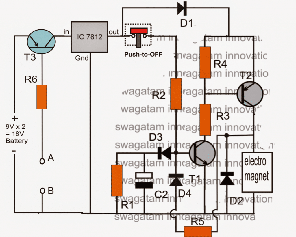
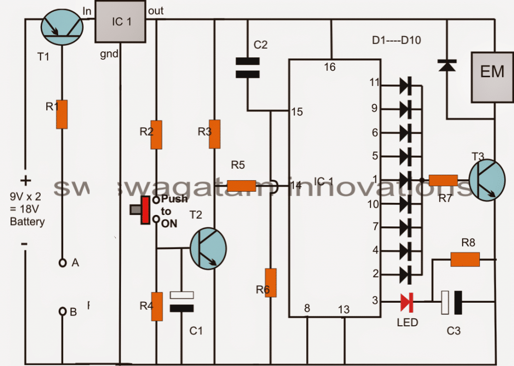 Parts List
R1 = 100 Ohms
R2, R6 = 100K
R4, R3, R5, R7 = 10K
R8 = 1M
C1 = to be calculated for acquring the required 2 seconds delay
C2 = 0.22uF
C3 = 0.5uF/25V
D1---D10 = 1N4007
T1 = TIP127
T2, T3 = BC547
IC1 = IC 4017
IC2 = 7812
Switch = push-to-ON type
EM = electromagnet
Feedback from Mr.
Marielle
Marielle van den Hoed6:24 PM (16 hours ago)
Parts List
R1 = 100 Ohms
R2, R6 = 100K
R4, R3, R5, R7 = 10K
R8 = 1M
C1 = to be calculated for acquring the required 2 seconds delay
C2 = 0.22uF
C3 = 0.5uF/25V
D1---D10 = 1N4007
T1 = TIP127
T2, T3 = BC547
IC1 = IC 4017
IC2 = 7812
Switch = push-to-ON type
EM = electromagnet
Feedback from Mr.
Marielle
Marielle van den Hoed6:24 PM (16 hours ago)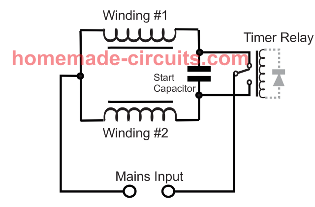
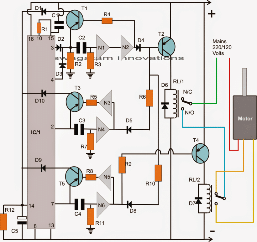
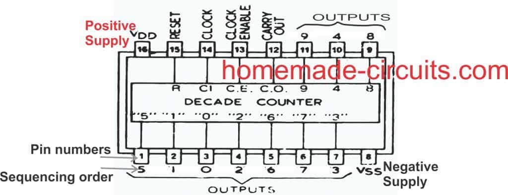 Complete Datasheet
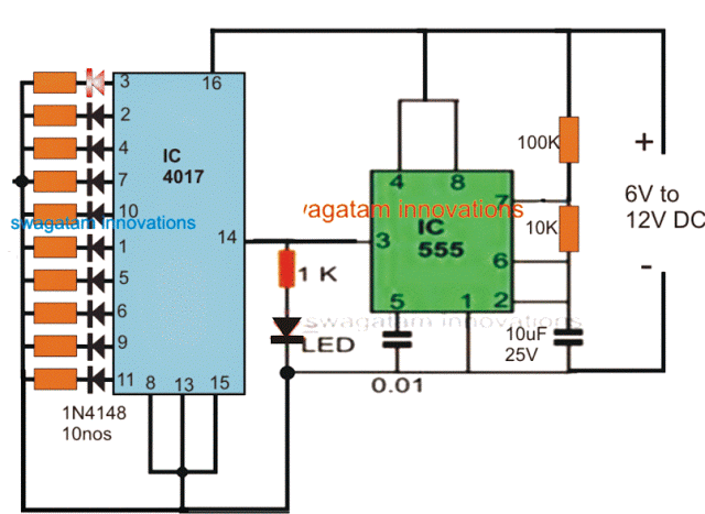 Video Clip:
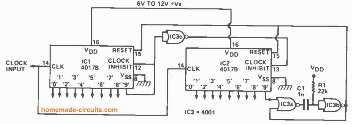 The diagram above shows how to connect two 4017s together to create a 10-to 17 stage counter/decoder.
It shows how to cascade two 4017 ICs to get 17 sequencing outputs instead of only 10 from a single IC.
The circuit is shown configured to divide by17.
The clock signal is supplied in parallel to IC1 and IC2. As soon as the count falls below 9, the '9' output of IC1 turnslow, causing the clock inhibit pinof IC2 to be set high through IC3c, preventing IC2 from being impacted by the clock signals.
The '9' output of IC1rises high when the 9th clock pulse comes, inhibiting IC1from further clocking action, while simultaneously driving the clock inhibit terminal of IC2 low through IC2c, allowing IC2 to respond to further clock signals.
When the 17th clock pulse arrives, the '9' output of IC2 swings high for a brief period, triggering the IC3a -IC3b 15uS monostable.
This 15us pulseresets both counters to the empty or '0' states.
After that, the counting sequence starts again byitself.
Because the '9' output of IC1 and the '0' and '9' outputs of IC2 are "lost" in the counting process, the circuit only has 17 counter/decoder stages available.
By connecting the "free" input pinof IC2a to the matching output pinof IC2, the circuit can be made tocount by any number between 10 and 17.
The diagram above shows how to connect two 4017s together to create a 10-to 17 stage counter/decoder.
It shows how to cascade two 4017 ICs to get 17 sequencing outputs instead of only 10 from a single IC.
The circuit is shown configured to divide by17.
The clock signal is supplied in parallel to IC1 and IC2. As soon as the count falls below 9, the '9' output of IC1 turnslow, causing the clock inhibit pinof IC2 to be set high through IC3c, preventing IC2 from being impacted by the clock signals.
The '9' output of IC1rises high when the 9th clock pulse comes, inhibiting IC1from further clocking action, while simultaneously driving the clock inhibit terminal of IC2 low through IC2c, allowing IC2 to respond to further clock signals.
When the 17th clock pulse arrives, the '9' output of IC2 swings high for a brief period, triggering the IC3a -IC3b 15uS monostable.
This 15us pulseresets both counters to the empty or '0' states.
After that, the counting sequence starts again byitself.
Because the '9' output of IC1 and the '0' and '9' outputs of IC2 are "lost" in the counting process, the circuit only has 17 counter/decoder stages available.
By connecting the "free" input pinof IC2a to the matching output pinof IC2, the circuit can be made tocount by any number between 10 and 17.
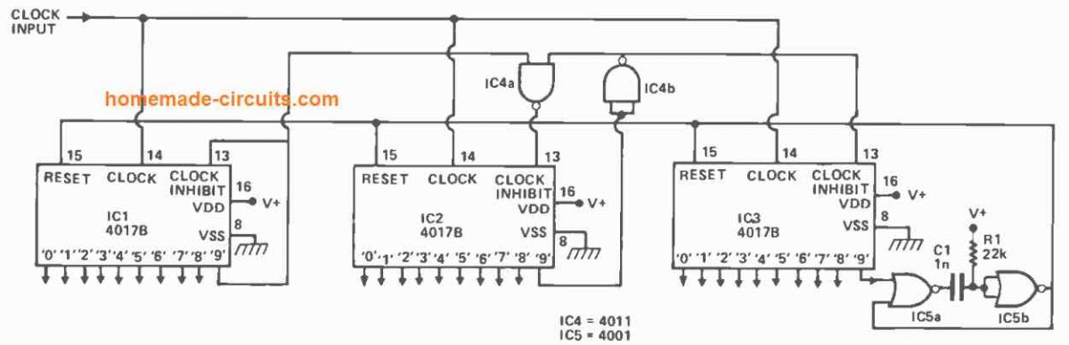 The configurationfor creating an 18to 25 stage counter/decoder from three 4017s can be seen in the diagram above.
IC3 is inhibited by IC4b and IC2's low output '9,' whereas IC2 is inhibited by IC4a and IC1's low output '9,' untilthe 9th clock pulse.
Between the 10th and 17th clock pulses, IC1is inhibited by its high '9' output, while IC3 is inhibited by IC4b and IC2's low output '9'.
Subsequently, between the 18th and 25th clock pulses, IC1 is inhibited by its high '9' output, and IC2 is inhibited through the high '9' outputs of IC1and IC2 using IC4c, and the wholecircuit is reset to the '0' state by means ofthe IC5a and IC5b monostable.
The configurationfor creating an 18to 25 stage counter/decoder from three 4017s can be seen in the diagram above.
IC3 is inhibited by IC4b and IC2's low output '9,' whereas IC2 is inhibited by IC4a and IC1's low output '9,' untilthe 9th clock pulse.
Between the 10th and 17th clock pulses, IC1is inhibited by its high '9' output, while IC3 is inhibited by IC4b and IC2's low output '9'.
Subsequently, between the 18th and 25th clock pulses, IC1 is inhibited by its high '9' output, and IC2 is inhibited through the high '9' outputs of IC1and IC2 using IC4c, and the wholecircuit is reset to the '0' state by means ofthe IC5a and IC5b monostable.
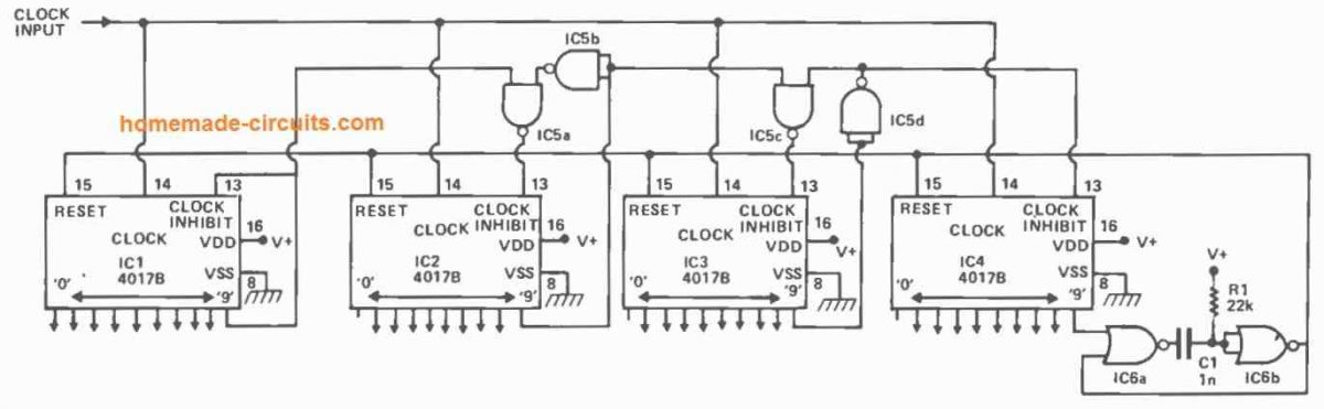 Using a divide-by-33 operation, the above setup shows how to make a 26 to 33 stage counter/decoder set.
By interposing extra IC2-1C5a-1C5b stages between 1C2 and 1C3, this design may be extended to provide a nynumber of decoded output stages.
Each subsequent 40178 stage adds eight decoded outputs to the system.
Using a divide-by-33 operation, the above setup shows how to make a 26 to 33 stage counter/decoder set.
By interposing extra IC2-1C5a-1C5b stages between 1C2 and 1C3, this design may be extended to provide a nynumber of decoded output stages.
Each subsequent 40178 stage adds eight decoded outputs to the system.

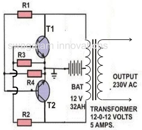 Well your search for such a circuit ends here.
The circuit of an inverter described here is perhaps the smallest as far its component count goes yet is powerful enough to fulfill most of your requirements.
Well your search for such a circuit ends here.
The circuit of an inverter described here is perhaps the smallest as far its component count goes yet is powerful enough to fulfill most of your requirements.
 Bend one end of the sheet as shown in the diagram.
Drill appropriate sized holes on to the bends so that it can be clamped firmly to the metal cabinet.
If you find it difficult to make this heatsink you can simply purchase from your local electronic shop shown below:
Bend one end of the sheet as shown in the diagram.
Drill appropriate sized holes on to the bends so that it can be clamped firmly to the metal cabinet.
If you find it difficult to make this heatsink you can simply purchase from your local electronic shop shown below:
 Also drill holes for fitting of the power transistors.
The holes are 3mm in diameter, TO-3 type of package size.
Fix the transistors tightly on to the heatsinks with the help of nuts and bolts.
Connect the resistors in a cross-coupled manner directly to the leads of the transistors as per the circuit diagram.
Now join the heatsink, transistor, resistor assembly to the secondary winding of the transformer.
Fix the whole circuit assembly along with the transformer inside a sturdy, well ventilated metal enclosure.
Fit the output and input sockets, fuse holder etc.
externally to the cabinet and connect them appropriately to the circuit assembly.
Once the above heatsink installation is over, you simply need to interconnect a few high watt resistors and the 2N3055 (on heatsink) with the selected transformer as given in the following diagram.
Also drill holes for fitting of the power transistors.
The holes are 3mm in diameter, TO-3 type of package size.
Fix the transistors tightly on to the heatsinks with the help of nuts and bolts.
Connect the resistors in a cross-coupled manner directly to the leads of the transistors as per the circuit diagram.
Now join the heatsink, transistor, resistor assembly to the secondary winding of the transformer.
Fix the whole circuit assembly along with the transformer inside a sturdy, well ventilated metal enclosure.
Fit the output and input sockets, fuse holder etc.
externally to the cabinet and connect them appropriately to the circuit assembly.
Once the above heatsink installation is over, you simply need to interconnect a few high watt resistors and the 2N3055 (on heatsink) with the selected transformer as given in the following diagram.
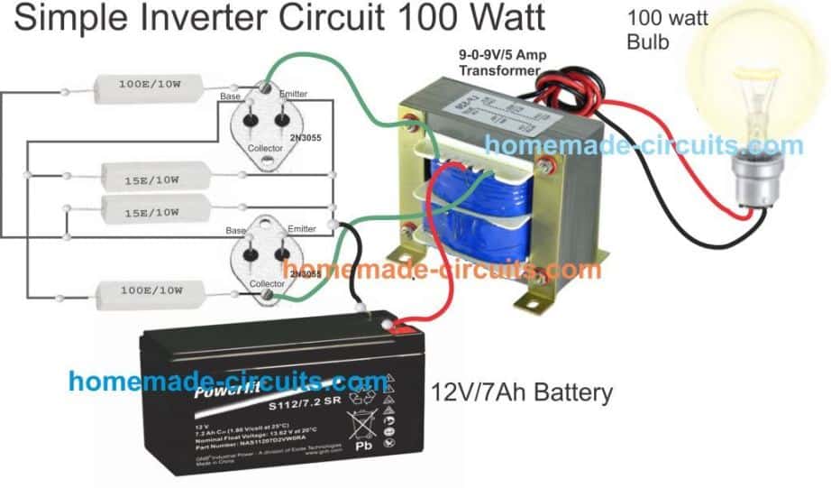 After the above wiring is completed, it's time to hook it up with a 12V 7Ah battery, with a 60 watt lamp attached at the transformer secondary.
When switched ON the result would be an instant illumination of the load with an astonishing brightness.
Here the key element is the transformer, make sure the transformer is genuinely rated at 5 amp, otherwise you may find the output power a lot lesser than the expectation.
I can tell this from my experience, I built this unit twice, once when I was in college, and the second time recently in the year 2015. Although I was more experienced during the recent venture I could not get the awesome power that I had acquired from my previous unit.
The reason was simple, the previous transformer was a robust custom built 9-0-9V 5 amp transformer, compared to the new one in which I had used probably a falsely rated 5 amp, which was actually only 3 amp with its output.
After the above wiring is completed, it's time to hook it up with a 12V 7Ah battery, with a 60 watt lamp attached at the transformer secondary.
When switched ON the result would be an instant illumination of the load with an astonishing brightness.
Here the key element is the transformer, make sure the transformer is genuinely rated at 5 amp, otherwise you may find the output power a lot lesser than the expectation.
I can tell this from my experience, I built this unit twice, once when I was in college, and the second time recently in the year 2015. Although I was more experienced during the recent venture I could not get the awesome power that I had acquired from my previous unit.
The reason was simple, the previous transformer was a robust custom built 9-0-9V 5 amp transformer, compared to the new one in which I had used probably a falsely rated 5 amp, which was actually only 3 amp with its output.
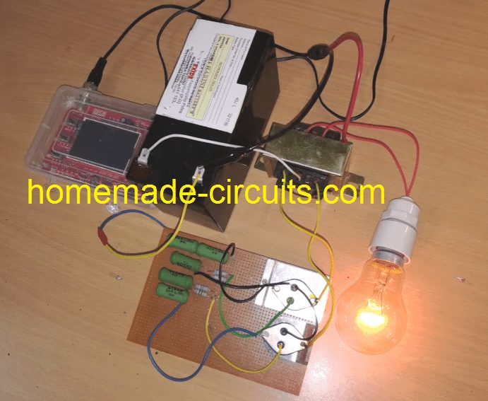
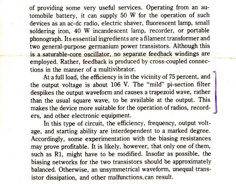 Output Waveform better than square wave (Reasonably suitable for all electronic appliances))
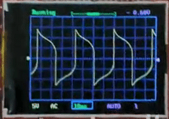
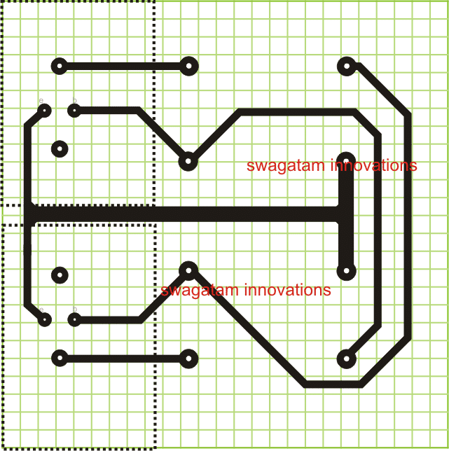
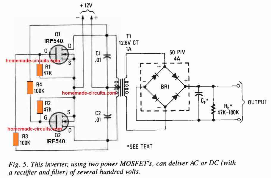 MOSFETs Q1 and Q2 can be any high power Nchannel FETs.
Do not forget to apply heat sink to the MOSFETs Q1 and Q2. Capacitors C1 and C2 are positioned in order to suppress high voltage reverse spikes from the transformer.
You can use any nearby value for the resistors R1-R4 having a tolerance of �� 20% to the shown values in the diagram.
The circuit is perfect to power a tube circuit, or it could be coupled with a step-up transformer to generate a spark gap, a Jacob's Ladder, or, by adjusting the frequency, it could be accustomed to energize a Tesla coil.
MOSFETs Q1 and Q2 can be any high power Nchannel FETs.
Do not forget to apply heat sink to the MOSFETs Q1 and Q2. Capacitors C1 and C2 are positioned in order to suppress high voltage reverse spikes from the transformer.
You can use any nearby value for the resistors R1-R4 having a tolerance of �� 20% to the shown values in the diagram.
The circuit is perfect to power a tube circuit, or it could be coupled with a step-up transformer to generate a spark gap, a Jacob's Ladder, or, by adjusting the frequency, it could be accustomed to energize a Tesla coil.
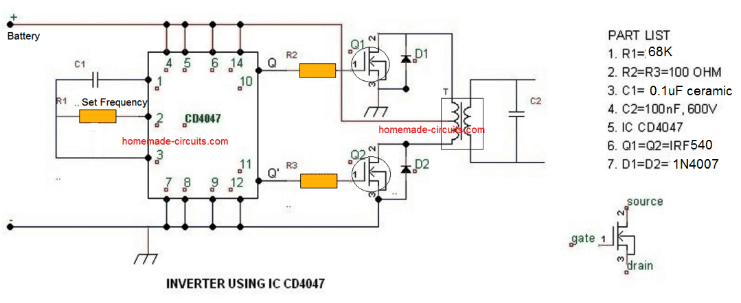 As shown above a simple yet useful little inverter can be built using just a single IC 4047.
The IC 4047 is a versatile single IC oscillator, which will produce precise ON/OFF periods across its output pin#10 and pin#11. The frequency here could be determined by accurately calculating the resistor R1 and capacitor C1. These components determine the oscillation frequency at the output of the IC which in turn sets the output 220V AC frequency of this inverter circuit.
It may set at 50Hz or 60Hz as per individual preference.
The battery, mosfet and the transformer can be modified or upgraded as per the required output power specification of the inverter.
For calculating the RC values, and the output frequency please refer to the datasheet of the IC
As shown above a simple yet useful little inverter can be built using just a single IC 4047.
The IC 4047 is a versatile single IC oscillator, which will produce precise ON/OFF periods across its output pin#10 and pin#11. The frequency here could be determined by accurately calculating the resistor R1 and capacitor C1. These components determine the oscillation frequency at the output of the IC which in turn sets the output 220V AC frequency of this inverter circuit.
It may set at 50Hz or 60Hz as per individual preference.
The battery, mosfet and the transformer can be modified or upgraded as per the required output power specification of the inverter.
For calculating the RC values, and the output frequency please refer to the datasheet of the IC
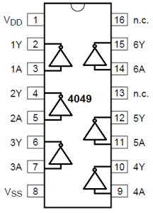
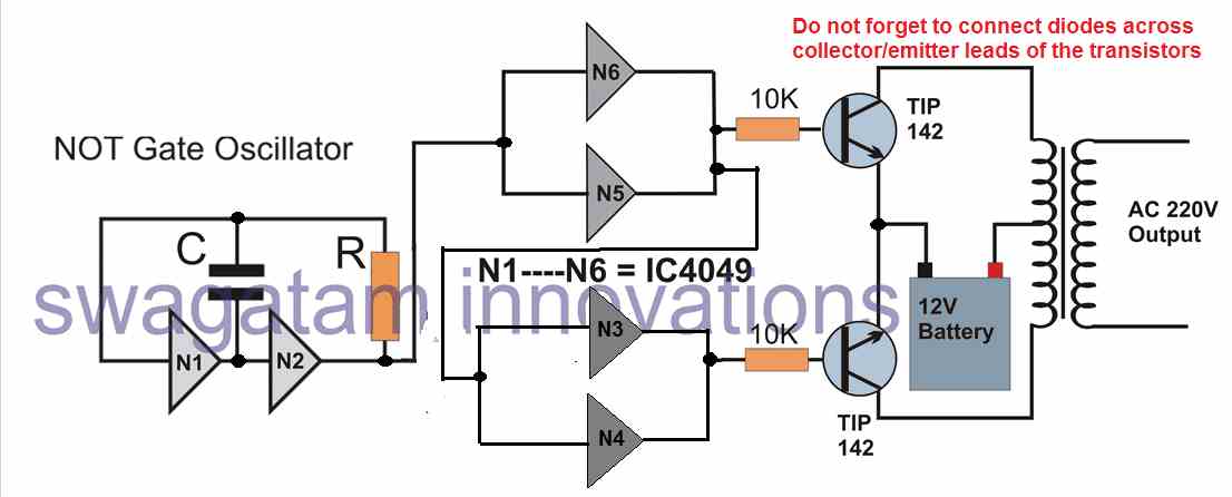 In this simple inverter circuit we use a single IC 4049 which includes 6 NOT gates or 6 inverters inside.
In the diagram above N1----N6 signify the 6 gates which are configured as oscillator and buffer stages.
The NOT gates N1 and N2 are basically used for the oscillator stage, the C and R can be selected and fixed for determining the 50Hz or 60 Hz frequency as per country specs
The remaining gates N3 to N6 are adjusted and configured as buffers and inverters so that the ultimate output results in producing alternating switching pulses for the power transistors.
The configuration also ensures that no gates are left unused and idle, which may otherwise require their inputs to be terminated separately across a supply line.
The transformer and battery may be selected as per the power requirement or the load wattage specifications.
The output will be purely a square wave output.
Formula for calculating frequency is given as:
f = 1 /1.2RC,
where R will be in Ohms and F in Farads
In this simple inverter circuit we use a single IC 4049 which includes 6 NOT gates or 6 inverters inside.
In the diagram above N1----N6 signify the 6 gates which are configured as oscillator and buffer stages.
The NOT gates N1 and N2 are basically used for the oscillator stage, the C and R can be selected and fixed for determining the 50Hz or 60 Hz frequency as per country specs
The remaining gates N3 to N6 are adjusted and configured as buffers and inverters so that the ultimate output results in producing alternating switching pulses for the power transistors.
The configuration also ensures that no gates are left unused and idle, which may otherwise require their inputs to be terminated separately across a supply line.
The transformer and battery may be selected as per the power requirement or the load wattage specifications.
The output will be purely a square wave output.
Formula for calculating frequency is given as:
f = 1 /1.2RC,
where R will be in Ohms and F in Farads
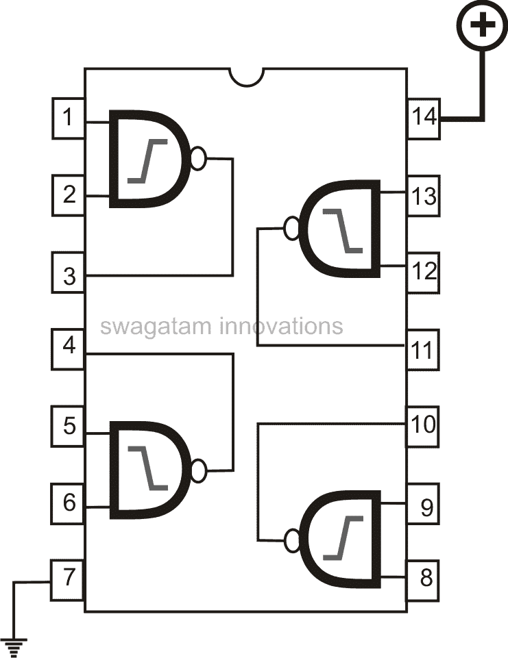 IC 4093 pin details
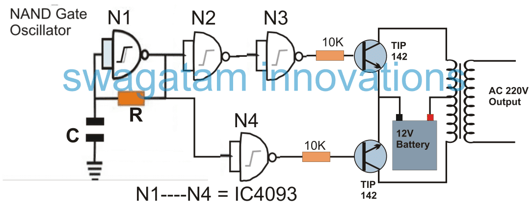 Quite similar to the previous NOT gate inveter, the NAND gate based simple inverter shown above can be built using a single 4093 IC.
The gates N1 to N4 signify the 4 gates inside the IC 4093.
N1, is wired as an oscillator circuit, for generating the required 50 or 60Hz pulses.
These are appropriately inverted and buffered using the remaining gates N2, N3, N4 in order to finally deliver the alternately switching frequency across the bases of the power BJTs, which in turn switch the power transformer at the supplied rate for generating the required 220V or 120V AC at the output.
Although any NAND gate IC would work here, using the IC 4093 is recommended since it features Schmidt trigger facility, which ensures a slight lag in switching and helps creating a kind of dead-time across the switching outputs, making sure that the power devices are never switched ON together even for a fraction of a second.
Quite similar to the previous NOT gate inveter, the NAND gate based simple inverter shown above can be built using a single 4093 IC.
The gates N1 to N4 signify the 4 gates inside the IC 4093.
N1, is wired as an oscillator circuit, for generating the required 50 or 60Hz pulses.
These are appropriately inverted and buffered using the remaining gates N2, N3, N4 in order to finally deliver the alternately switching frequency across the bases of the power BJTs, which in turn switch the power transformer at the supplied rate for generating the required 220V or 120V AC at the output.
Although any NAND gate IC would work here, using the IC 4093 is recommended since it features Schmidt trigger facility, which ensures a slight lag in switching and helps creating a kind of dead-time across the switching outputs, making sure that the power devices are never switched ON together even for a fraction of a second.
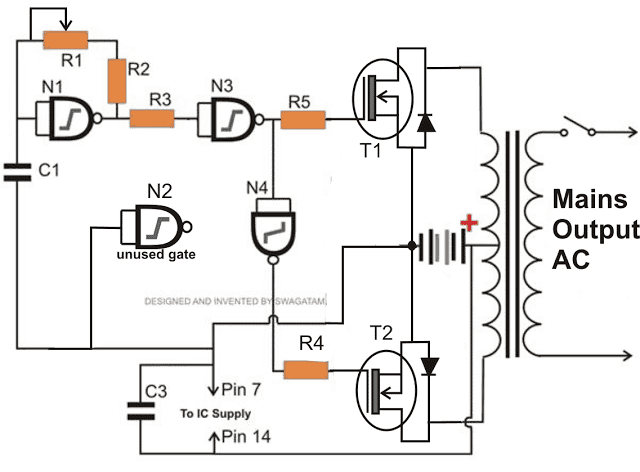
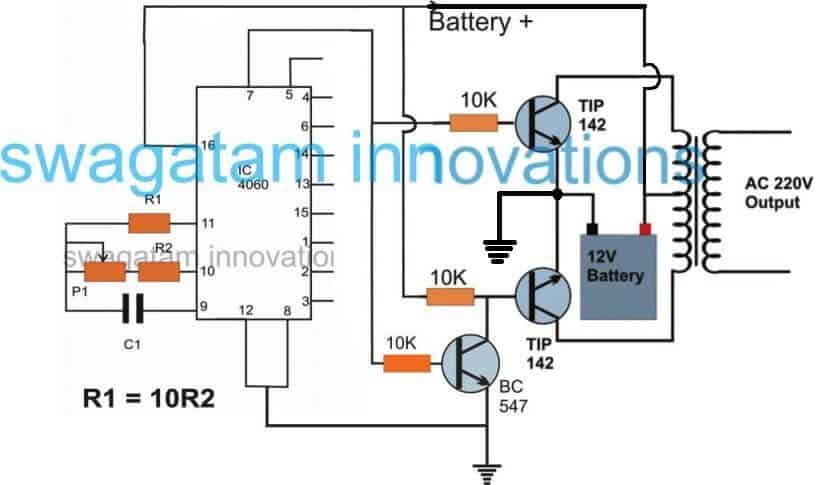 If you have a single 4060 IC in your electronic junk box, along with a transformer and a few power transistors, you are probably all set to create your simple power inverter circuit using these components.
The basic design of the proposed IC 4060 based inverter circuit can be visualized in the above diagram.
The concept is basically the same, we use the IC 4060 as an oscillator, and set its output to create alternately switching ON OFF pulses through an inverter BC547 transistors stage.
Just like IC 4047, the IC 4060 requires an external RC components for setting up its output frequency, however, the output from the IC 4060 are terminated into 10 individual pinouts in a specific order wherein the output generate frequency at a rate twice that of its preceding pinout.
Although you may find 10 separate outputs with a rate of 2X frequency rate across the IC output pinouts, we have selected the pin#7 since it delivers the fastest frequency rate among the rest and therefore may fulfil this using standard components for the RC network, which may be easily available to you no matter in which part of the globe you are situated in.
For calculating the RC values for R2 +P1 and C1 and the frequency you can use the formula as described below:
If you have a single 4060 IC in your electronic junk box, along with a transformer and a few power transistors, you are probably all set to create your simple power inverter circuit using these components.
The basic design of the proposed IC 4060 based inverter circuit can be visualized in the above diagram.
The concept is basically the same, we use the IC 4060 as an oscillator, and set its output to create alternately switching ON OFF pulses through an inverter BC547 transistors stage.
Just like IC 4047, the IC 4060 requires an external RC components for setting up its output frequency, however, the output from the IC 4060 are terminated into 10 individual pinouts in a specific order wherein the output generate frequency at a rate twice that of its preceding pinout.
Although you may find 10 separate outputs with a rate of 2X frequency rate across the IC output pinouts, we have selected the pin#7 since it delivers the fastest frequency rate among the rest and therefore may fulfil this using standard components for the RC network, which may be easily available to you no matter in which part of the globe you are situated in.
For calculating the RC values for R2 +P1 and C1 and the frequency you can use the formula as described below:
 Or another way is through the following formula:
f(osc) = 1 / 2.3 x Rt x Ct
Rt is in Ohms, Ct in Farads
More info can be obtained from this article
Here's yet another cool DIY inverter idea which is extremely reliable and uses ordinary parts for accomplishing a high power inverter design, and can be upgraded to any desired power level.
Let's learn more about this simple design
Or another way is through the following formula:
f(osc) = 1 / 2.3 x Rt x Ct
Rt is in Ohms, Ct in Farads
More info can be obtained from this article
Here's yet another cool DIY inverter idea which is extremely reliable and uses ordinary parts for accomplishing a high power inverter design, and can be upgraded to any desired power level.
Let's learn more about this simple design
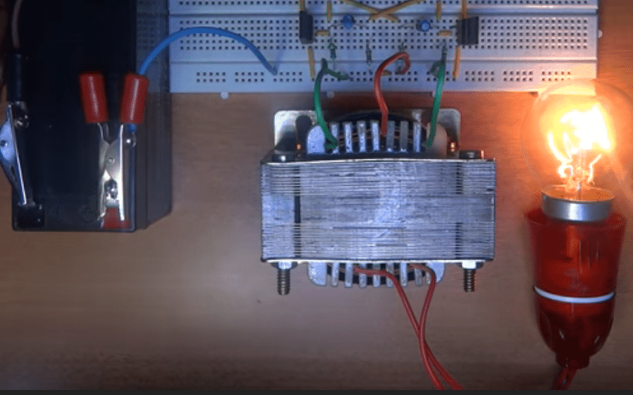
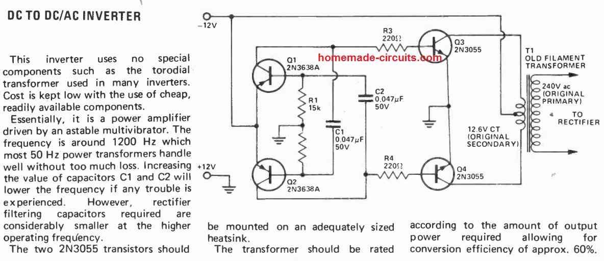
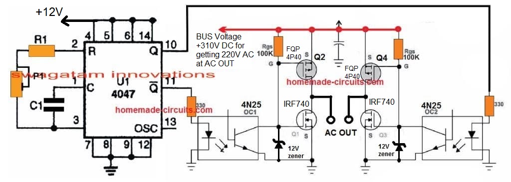 If you wish to employ some other oscillator stage as per your preference, in that case you can apply the following universal design.
This will allow you to integrate any desired oscillator stage and get the required 220 V push pull output.
Moreover it also has an integrated auto-changeover battery charger stage.
If you wish to employ some other oscillator stage as per your preference, in that case you can apply the following universal design.
This will allow you to integrate any desired oscillator stage and get the required 220 V push pull output.
Moreover it also has an integrated auto-changeover battery charger stage.
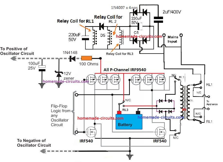 UNIVERSAL PUSH PULL MOSFET MODULE WHICH WILL INTERFACE WITH ANY DESIRED OSCILLATOR CIRCUIT
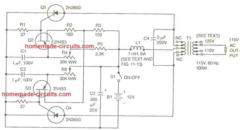 The transformer can be be any ordinary iron core 9-0-9 V to 220 V or 120 V step down transformer, connected in the reverse order.
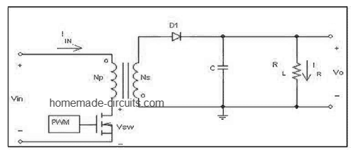 This type of flyback design could have a CCM (continuous conduction mode) or DCM (Discontinuous conduction mode) of operation based on how the power MOSFET T1 is configured.
Basically, in DCM mode we have the entire electrical energy stored in the transformer primary transferred across the secondary side each time the MOSFET is turned OFF during its switching cycles (also called the flyback period), leading to the primary side current reaching a zero potential before T1 is able to turn ON again in its next switching cycle.
In the CCM mode, the electrical energy stored in the primary does not get the opportunity to get fully transferred or induced across the secondary.
This is because, each of the subsequent switching pulses from the PWM controller turn ON T1 before the transformer has transferred its full stored energy to the load.
This implies that the flyback current (ILPK and ISEC) are never allowed to reach the zero potential during each of the switching cycles.
We can witness the difference between the two modes of operation in the following diagram through the current waveform patterns across the primary and secondary section of the transformer.
This type of flyback design could have a CCM (continuous conduction mode) or DCM (Discontinuous conduction mode) of operation based on how the power MOSFET T1 is configured.
Basically, in DCM mode we have the entire electrical energy stored in the transformer primary transferred across the secondary side each time the MOSFET is turned OFF during its switching cycles (also called the flyback period), leading to the primary side current reaching a zero potential before T1 is able to turn ON again in its next switching cycle.
In the CCM mode, the electrical energy stored in the primary does not get the opportunity to get fully transferred or induced across the secondary.
This is because, each of the subsequent switching pulses from the PWM controller turn ON T1 before the transformer has transferred its full stored energy to the load.
This implies that the flyback current (ILPK and ISEC) are never allowed to reach the zero potential during each of the switching cycles.
We can witness the difference between the two modes of operation in the following diagram through the current waveform patterns across the primary and secondary section of the transformer.
 Both DCM and CCM modes have their specific advantages, which may be learned from the following table:
 Compared to CCM, the DCM mode circuit demands greater levels of peak current in order to ensure optimal power across the secondary side of the transformer.
This in turn demands the primary side to be rated at higher RMS current, meaning the MOSFET needs to be rated at the specified higher range.
In cases where the design is required to be built with limited range of input current and components, then usually a CCM mode fyback is selected, allowing the design to employ relatively smaller filter capacitor, and lower conduction loss on the MOSFET and the transformer).
CCM becomes favorable for conditions where the input voltage is lower, while the current is higher ( over 6 ampere), designs which may be rated to work with over 50 watt power, except for outputs at 5V wherein the wattage spec could be lower than 50 watts.
Compared to CCM, the DCM mode circuit demands greater levels of peak current in order to ensure optimal power across the secondary side of the transformer.
This in turn demands the primary side to be rated at higher RMS current, meaning the MOSFET needs to be rated at the specified higher range.
In cases where the design is required to be built with limited range of input current and components, then usually a CCM mode fyback is selected, allowing the design to employ relatively smaller filter capacitor, and lower conduction loss on the MOSFET and the transformer).
CCM becomes favorable for conditions where the input voltage is lower, while the current is higher ( over 6 ampere), designs which may be rated to work with over 50 watt power, except for outputs at 5V wherein the wattage spec could be lower than 50 watts.
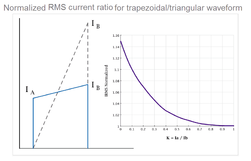 The image above indicates the current response on primary side of the flyback modes and the corresponding relationship between their triangular and trapezoidal waveforms.
IA on the triangular waveform indicates the minimal initialization point which may be seen as zero, at the beginning of the switch ON period of the MOSFET, and also a higher current peak level persistent in the primary winding of the transformer at the time until the MOSFET is switched ON again, during the CCM mode of operation.
IB may be perceived as the finish point of the current magnitude while the mosfet switch is turned ON (Ton interval).
The normalized current value IRMS can be seen as the function of the K factor (IA/IB) over the Y axis.
This may be used as the multiplier whenever resistive losses needs to be calculated for an assorted number of wave shapes with reference to a trapezoidal waveform having a flat upper waveform.
This also demonstrates the extra unavoidable DC conduction losses of the transformer winding and the transistors or diodes as a current waveform function.
Utilizing these advises the designer will be able to prevent as good as 10 to 15% conduction losses with such well calculated converter design.
Considering the above criteria may become significantly crucial for applications designed to handle high RMS currents, and demanding an optimal efficiency as the key features.
It may be possible to eliminate the extra copper losses, although that may demand a formidable core size for accommodating the essential bigger winding window area, in contrast to situations where only the core specifications become crucial.
As we have understood so far, a DCM mode of operation enables the use of a lower sized transformer, possesses greater transient response and works with minimal switching losses.
Therefore this mode becomes highly recommended for flyback circuits specified for higher output voltages with relatively lower ampere requirements.
Although it may be possible to design a flyback converter to work with DCM as well as CCM modes, one thing must be remembered that during the transition from DCM to CCM mode, this shifting function transforms into a 2-pole operation, giving rise to low impedance for the converter.
This situation makes it essential to incorporate additional design strategies, including various loop (feedback) and slope compensation with respect to the inner current loop system.
Practically this implies that we have to make sure that the converter is primarily designed for a CCM mode, yet is able to work with DCM mode when lighter loads are used at the output.
It may be interesting to know that by using advanced transformer models, it may become possible to enhance a CCM converter through cleaner and lighter load regulation, as well as high cross regulation over a wide range of load through a stepped-gap-transformer.
In such cases a small core gap is enforced by inserting a external element such as an insulation tape or paper, in order to induce high inductance initially, and also enable CCM operation with lighter loads.
We will discuss this elaborately some other time my subsequent articles.
Having such versatile DCM mode characteristics, no surprise this becomes the popular choice whenever a hassle free, efficient and low power SMPS is required to be designed.
In the following we will learn the step by step instructions regarding how to design a DCM mode flyback converter.
The image above indicates the current response on primary side of the flyback modes and the corresponding relationship between their triangular and trapezoidal waveforms.
IA on the triangular waveform indicates the minimal initialization point which may be seen as zero, at the beginning of the switch ON period of the MOSFET, and also a higher current peak level persistent in the primary winding of the transformer at the time until the MOSFET is switched ON again, during the CCM mode of operation.
IB may be perceived as the finish point of the current magnitude while the mosfet switch is turned ON (Ton interval).
The normalized current value IRMS can be seen as the function of the K factor (IA/IB) over the Y axis.
This may be used as the multiplier whenever resistive losses needs to be calculated for an assorted number of wave shapes with reference to a trapezoidal waveform having a flat upper waveform.
This also demonstrates the extra unavoidable DC conduction losses of the transformer winding and the transistors or diodes as a current waveform function.
Utilizing these advises the designer will be able to prevent as good as 10 to 15% conduction losses with such well calculated converter design.
Considering the above criteria may become significantly crucial for applications designed to handle high RMS currents, and demanding an optimal efficiency as the key features.
It may be possible to eliminate the extra copper losses, although that may demand a formidable core size for accommodating the essential bigger winding window area, in contrast to situations where only the core specifications become crucial.
As we have understood so far, a DCM mode of operation enables the use of a lower sized transformer, possesses greater transient response and works with minimal switching losses.
Therefore this mode becomes highly recommended for flyback circuits specified for higher output voltages with relatively lower ampere requirements.
Although it may be possible to design a flyback converter to work with DCM as well as CCM modes, one thing must be remembered that during the transition from DCM to CCM mode, this shifting function transforms into a 2-pole operation, giving rise to low impedance for the converter.
This situation makes it essential to incorporate additional design strategies, including various loop (feedback) and slope compensation with respect to the inner current loop system.
Practically this implies that we have to make sure that the converter is primarily designed for a CCM mode, yet is able to work with DCM mode when lighter loads are used at the output.
It may be interesting to know that by using advanced transformer models, it may become possible to enhance a CCM converter through cleaner and lighter load regulation, as well as high cross regulation over a wide range of load through a stepped-gap-transformer.
In such cases a small core gap is enforced by inserting a external element such as an insulation tape or paper, in order to induce high inductance initially, and also enable CCM operation with lighter loads.
We will discuss this elaborately some other time my subsequent articles.
Having such versatile DCM mode characteristics, no surprise this becomes the popular choice whenever a hassle free, efficient and low power SMPS is required to be designed.
In the following we will learn the step by step instructions regarding how to design a DCM mode flyback converter.
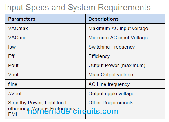 We know that the efficiency parameter is the crucial one that needs to be decided first, the easiest way is to go about is to set a target of around 75% to 80%, even if your design is a low cost design.
The switching frequency denoted as
Fsw generally has to be compromised while getting the best of transformer size and losses incurred due to switching, and EMI.
Which implies one may need to decide on a switching frequency at least below 150kHz.
Typically this may be selected between a 50kHz and 100kHz range.
Furthermore, in case more than one output is required to be included for the design, the maximum power value Pout will need to be adjusted as the combined value of the two outputs.
You may find interesting to know that until recent times the most popular conventional SMPS designs used to have the mosfet and the PWM switching controller as two different isolated stages, integrated together over a PCB layout, but nowadays in modern SMPS units these two stages can be found embedded inside one package and manufactured as single ICs.
Mainly, the parameters which are typically considered while designing a flyback SMPS converter are 1) The application or the load specifications, 2) Cost 3) Standby power, and 4) Additional protection features.
When embedded ICs are used, usually things become a lot easier, as it only requires the transformer and a few external passive component to be calculated for designing an optimal flyback converter.
Let��s get into the details regarding the involved calculations for designing a flaback SMPS.
Calculating the Input Capacitor Cin, and the Input DC Voltage Range
Depending on input voltage and power specifications, the standard rule for selecting Cin which is also referred to as a DC link capacitor can be learned from the following explanations:
We know that the efficiency parameter is the crucial one that needs to be decided first, the easiest way is to go about is to set a target of around 75% to 80%, even if your design is a low cost design.
The switching frequency denoted as
Fsw generally has to be compromised while getting the best of transformer size and losses incurred due to switching, and EMI.
Which implies one may need to decide on a switching frequency at least below 150kHz.
Typically this may be selected between a 50kHz and 100kHz range.
Furthermore, in case more than one output is required to be included for the design, the maximum power value Pout will need to be adjusted as the combined value of the two outputs.
You may find interesting to know that until recent times the most popular conventional SMPS designs used to have the mosfet and the PWM switching controller as two different isolated stages, integrated together over a PCB layout, but nowadays in modern SMPS units these two stages can be found embedded inside one package and manufactured as single ICs.
Mainly, the parameters which are typically considered while designing a flyback SMPS converter are 1) The application or the load specifications, 2) Cost 3) Standby power, and 4) Additional protection features.
When embedded ICs are used, usually things become a lot easier, as it only requires the transformer and a few external passive component to be calculated for designing an optimal flyback converter.
Let��s get into the details regarding the involved calculations for designing a flaback SMPS.
Calculating the Input Capacitor Cin, and the Input DC Voltage Range
Depending on input voltage and power specifications, the standard rule for selecting Cin which is also referred to as a DC link capacitor can be learned from the following explanations:
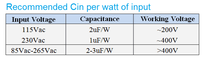 In order to ensure a broad range of operation, a 2uF per watt or higher value may be chosen for a DC link capacitor, which will enable you to have a good quality range for this component.
Next, it may be required to determine the minimum DC input voltage which may be obtained by solving:
In order to ensure a broad range of operation, a 2uF per watt or higher value may be chosen for a DC link capacitor, which will enable you to have a good quality range for this component.
Next, it may be required to determine the minimum DC input voltage which may be obtained by solving:
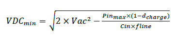 Where the discharge becomes the duty ratio of the DC link capacitor, which may be roughly around 0.2
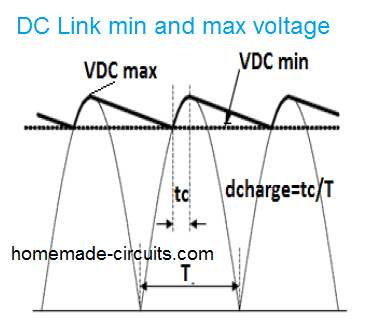 In the figure above we can visualize the DC link capacitor voltage.
As shown, the input voltage arises during maximum output power and minimum input AC voltage, whereas the maximum DC input voltage arises during minimum input power (absence of load) and during maximum input AC voltage.
During no load condition, we are able to see a maximum DC input voltage, during which the capacitor charges at the peak level of the AC input voltage, and these values can be expressed with the following equation:
In the figure above we can visualize the DC link capacitor voltage.
As shown, the input voltage arises during maximum output power and minimum input AC voltage, whereas the maximum DC input voltage arises during minimum input power (absence of load) and during maximum input AC voltage.
During no load condition, we are able to see a maximum DC input voltage, during which the capacitor charges at the peak level of the AC input voltage, and these values can be expressed with the following equation:
 Step3:
Evaluating the Flyback induced voltage VR, and the maximum voltage stress on the MOSFET VDS.
The Flyback induced voltage VR could be understood as the voltage induced across the primary side of the transformer when the mosfet Q1 is in switched OFF condition.
The above function in turn impacts maximum VDS rating of the mosfet, which may be confirmed and identified by solving the following equation:
Step3:
Evaluating the Flyback induced voltage VR, and the maximum voltage stress on the MOSFET VDS.
The Flyback induced voltage VR could be understood as the voltage induced across the primary side of the transformer when the mosfet Q1 is in switched OFF condition.
The above function in turn impacts maximum VDS rating of the mosfet, which may be confirmed and identified by solving the following equation:
 Where, Vspike is the voltage spike generated due to transformer leakage inductance.
To start with, a 30% Vspike out of VDSmax can be taken.
The following list tells us how much reflected voltage or induced voltage may be recommended for a 650V to 800V rated MOSFET, and having an initial limit value VR lower than 100V for an expected vast input voltage range.
Where, Vspike is the voltage spike generated due to transformer leakage inductance.
To start with, a 30% Vspike out of VDSmax can be taken.
The following list tells us how much reflected voltage or induced voltage may be recommended for a 650V to 800V rated MOSFET, and having an initial limit value VR lower than 100V for an expected vast input voltage range.
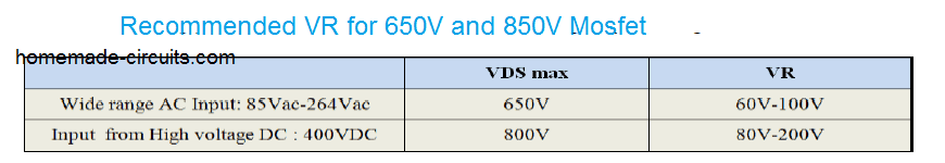 Picking the right VR can be a bargain between the level of voltage stress over the secondary rectifier, and the primary side mosfet specifications.
If VR is selected very high through an increased turn ratio, would give rise to a bigger VDSmax, but a lower level of voltage stress on the secondary side diode.
And if VR is selected too small through a smaller turn ratio, would cause VDSmax to be smaller, but would result in an increase in the stress level on the secondary diode.
A bigger primary side VDSmax would assure not only lower stress level on the secondary side diode and reduction in primary current, but will also allow a cost effective design to be implemented.
Picking the right VR can be a bargain between the level of voltage stress over the secondary rectifier, and the primary side mosfet specifications.
If VR is selected very high through an increased turn ratio, would give rise to a bigger VDSmax, but a lower level of voltage stress on the secondary side diode.
And if VR is selected too small through a smaller turn ratio, would cause VDSmax to be smaller, but would result in an increase in the stress level on the secondary diode.
A bigger primary side VDSmax would assure not only lower stress level on the secondary side diode and reduction in primary current, but will also allow a cost effective design to be implemented.
 Step4:
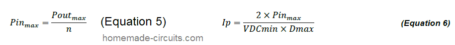 Once the above is achieved we can go ahead and calculate the primary inductance using the following formula, within the maximum duty cycle boundaries.
 Care must be taken regarding the flyback, it must not go into the CCM mode due to any form of excess loading conditions, and for this maximum power specification should be considered while calculating Poutmax in Equation#5. The mentioned condition can also occur in case inductance is increased over the Lprimax value, so take a note of these.
Step5:
Care must be taken regarding the flyback, it must not go into the CCM mode due to any form of excess loading conditions, and for this maximum power specification should be considered while calculating Poutmax in Equation#5. The mentioned condition can also occur in case inductance is increased over the Lprimax value, so take a note of these.
Step5:
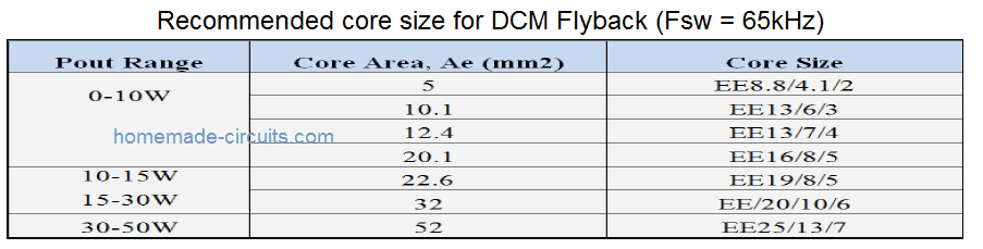 Once you are done with the selection of the core size, it is time to select the correct bobbin, which could be acquired as per the core datasheet.
Additional properties of the bobbin such as number of pins, PCB mount or SMD, horizontal or vertical positioning all these may also need to be considered as the preferred design
The core material is also crucial and must be selected based on the frequency, magnetic flux density, and core losses.
To begin with you can try variants with the name 3F3, 3C96, or TP4A, remember the names of available core material may be different for identical types depending on the particular manufacture.
Once you are done with the selection of the core size, it is time to select the correct bobbin, which could be acquired as per the core datasheet.
Additional properties of the bobbin such as number of pins, PCB mount or SMD, horizontal or vertical positioning all these may also need to be considered as the preferred design
The core material is also crucial and must be selected based on the frequency, magnetic flux density, and core losses.
To begin with you can try variants with the name 3F3, 3C96, or TP4A, remember the names of available core material may be different for identical types depending on the particular manufacture.
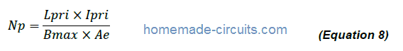 Where the term Bmax signifies the operating maximum flux density, Lpri tells you about the primary inductance, Ipri becomes the primary peak current, while Ae identifies the cross sectional area of the selected core type.
It must remembered that the Bmax should never be allowed to exceed the saturating flux density (Bsat) as specified in the datasheet of the core material.
You may find slight variances in Bsat for ferrite cores depending on specifications such as material type and temperature; however a majority of these will have a value near to 400mT.
If you find no detailed reference data, you may go with a Bmax of 300mT.
Although selecting higher Bmax may assist in having reduced number of primary turns and lower conduction, core loss may significantly increase.
Try to optimize between the values of these parameters, such that core loss and copper loss both are kept within acceptable limits.
Step 6:
Where the term Bmax signifies the operating maximum flux density, Lpri tells you about the primary inductance, Ipri becomes the primary peak current, while Ae identifies the cross sectional area of the selected core type.
It must remembered that the Bmax should never be allowed to exceed the saturating flux density (Bsat) as specified in the datasheet of the core material.
You may find slight variances in Bsat for ferrite cores depending on specifications such as material type and temperature; however a majority of these will have a value near to 400mT.
If you find no detailed reference data, you may go with a Bmax of 300mT.
Although selecting higher Bmax may assist in having reduced number of primary turns and lower conduction, core loss may significantly increase.
Try to optimize between the values of these parameters, such that core loss and copper loss both are kept within acceptable limits.
Step 6:
 Where Np is the primary turns, and Ns is the secondary number of turns, Vout signifies the output voltage, and VD tells us regarding the voltage drop across the secondary diode.
For calculating the turns for the auxiliary outputs for a desired Vcc value, the following formula can be used:
Where Np is the primary turns, and Ns is the secondary number of turns, Vout signifies the output voltage, and VD tells us regarding the voltage drop across the secondary diode.
For calculating the turns for the auxiliary outputs for a desired Vcc value, the following formula can be used:
 An auxiliary winding becomes crucial in all flyback converters for supplying the initial start-up supply to the control IC.
This supply VCC is normally used for powering the switching IC on the primary side and could be fixed as per the value given in the datasheet of the IC.
If the calculation gives a non-integer value, simply round it of by using the upper integer value just above this non integer number.
An auxiliary winding becomes crucial in all flyback converters for supplying the initial start-up supply to the control IC.
This supply VCC is normally used for powering the switching IC on the primary side and could be fixed as per the value given in the datasheet of the IC.
If the calculation gives a non-integer value, simply round it of by using the upper integer value just above this non integer number.
 As a starting point, a current density of 150 to 400 circular mil per Ampere, could be utilized for determining the gauge of the wire.
The following table shows the reference for selecting the appropriate wire gauge using 200M/A, as per the RMS current value.
It also shows you the diameter of the wire and the basic insulation for an assorted gauge of super enameled copper wires.
As a starting point, a current density of 150 to 400 circular mil per Ampere, could be utilized for determining the gauge of the wire.
The following table shows the reference for selecting the appropriate wire gauge using 200M/A, as per the RMS current value.
It also shows you the diameter of the wire and the basic insulation for an assorted gauge of super enameled copper wires.
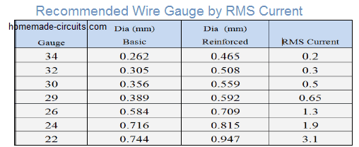 Step8:
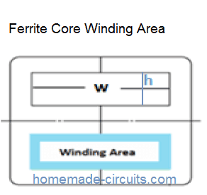 The winding layout is crucial since the working performance, and the reliability of the transformer, significantly depends on it.
It is recommended to employ a sandwich layout or structure for the winding in order to restrict inductance leakage, as indicated in Fig5.
Also in order to satisfy and conform with the international safety rules, the design must have sufficient range of insulation across the primary and secondary layers of winding.
This may be assured by employing margin-wound structure, or by using a secondary wire having triple insulated wire rating, as shown in the following respective figure
The winding layout is crucial since the working performance, and the reliability of the transformer, significantly depends on it.
It is recommended to employ a sandwich layout or structure for the winding in order to restrict inductance leakage, as indicated in Fig5.
Also in order to satisfy and conform with the international safety rules, the design must have sufficient range of insulation across the primary and secondary layers of winding.
This may be assured by employing margin-wound structure, or by using a secondary wire having triple insulated wire rating, as shown in the following respective figure
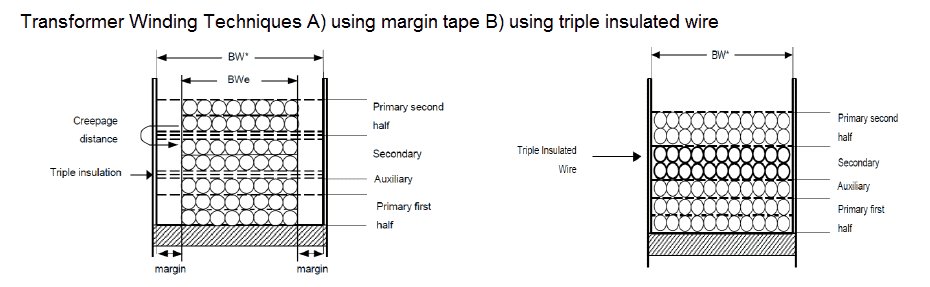 Employing triple insulated wire for the secondary winding becomes the easier option for quickly affirming the international safety laws concerning flyback SMPS designs.
However such reinforced wires may have a bit higher thickness compared to the normal variant compelling the winding to occupy more space, and may require additional effort to accommodate within the selected bobbin.
Step 9
Employing triple insulated wire for the secondary winding becomes the easier option for quickly affirming the international safety laws concerning flyback SMPS designs.
However such reinforced wires may have a bit higher thickness compared to the normal variant compelling the winding to occupy more space, and may require additional effort to accommodate within the selected bobbin.
Step 9
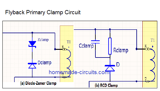 These are namely RCD clamp, and Diode/Zener clamp, where the latter is much easier to configure and implement than the first option.
In this clamp circuit we use a combination of a rectifier diode and a high voltage Zener diode such as a TVS (transient voltage suppressor) for clamping the surge spike.
The function of the Zener diode is to efficiently clip or limit the voltage spike until the leakage voltage is fully shunted through the Zener diode.
The advantage of a diode Zener clamp is that the circuit activates and clamps only when the combined value of VR and Vspike exceeds the breakdown spec of the Zener diode, and conversely, as long as the spike is below the Zener breakdown or a safe level, the clamp may not trigger at all, not allowing any unnecessary power dissipation.
These are namely RCD clamp, and Diode/Zener clamp, where the latter is much easier to configure and implement than the first option.
In this clamp circuit we use a combination of a rectifier diode and a high voltage Zener diode such as a TVS (transient voltage suppressor) for clamping the surge spike.
The function of the Zener diode is to efficiently clip or limit the voltage spike until the leakage voltage is fully shunted through the Zener diode.
The advantage of a diode Zener clamp is that the circuit activates and clamps only when the combined value of VR and Vspike exceeds the breakdown spec of the Zener diode, and conversely, as long as the spike is below the Zener breakdown or a safe level, the clamp may not trigger at all, not allowing any unnecessary power dissipation.
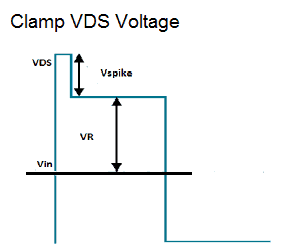 Referring to the figure above, to ensure VR = Vspike, the following formula could be used
 Where Lleak signifies the inductance of the transformer, and could be found by making a short circuit across the secondary winding, or alternatively, a rule of thumb value could be incorporated by applying 2 to 4% of the primary inductance value.
In this case the capacitor Cclamp should be substantially large inhibit a rise in voltage during the absorption period of the leakage energy.
The value of Cclamp may be selected between 100pF to 4.7nF, the energy stored inside this capacitor will be discharged and refreshed by Rclamp quickly during eacj switching cycle.
Step10
Where Lleak signifies the inductance of the transformer, and could be found by making a short circuit across the secondary winding, or alternatively, a rule of thumb value could be incorporated by applying 2 to 4% of the primary inductance value.
In this case the capacitor Cclamp should be substantially large inhibit a rise in voltage during the absorption period of the leakage energy.
The value of Cclamp may be selected between 100pF to 4.7nF, the energy stored inside this capacitor will be discharged and refreshed by Rclamp quickly during eacj switching cycle.
Step10
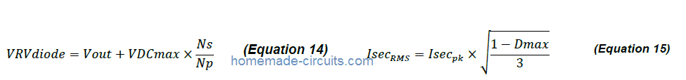 This may be calculated using the formula shown above.
Make sure to select the specifications such that the maximum reverse voltage or the VRRM of the diode is not less than 30% than the VRVdiode, and also ensure that the IF or the avalanche forward current spec is minimum 50% greater than the IsecRMS.
Preferably go for a schottky diode to minimize conduction losses.
With a DCM circuit the Flyback peak current may be high, therefore try selecting a diode having a lower forward voltage and a relatively higher current specs, with regards to the desired efficiency level.
Step11
This may be calculated using the formula shown above.
Make sure to select the specifications such that the maximum reverse voltage or the VRRM of the diode is not less than 30% than the VRVdiode, and also ensure that the IF or the avalanche forward current spec is minimum 50% greater than the IsecRMS.
Preferably go for a schottky diode to minimize conduction losses.
With a DCM circuit the Flyback peak current may be high, therefore try selecting a diode having a lower forward voltage and a relatively higher current specs, with regards to the desired efficiency level.
Step11
 Where Ncp signifies the number of primary side clock pulses required by the control feedback for controlling the duty from the specified maximum and minimum values.
This may typically require around 10 to 20 switching cycles.
Iout refers to the maximum output current (Iout = Poutmax / Vout).
To identify the maximum RMS value for the output capacitor, use the following formula:
Where Ncp signifies the number of primary side clock pulses required by the control feedback for controlling the duty from the specified maximum and minimum values.
This may typically require around 10 to 20 switching cycles.
Iout refers to the maximum output current (Iout = Poutmax / Vout).
To identify the maximum RMS value for the output capacitor, use the following formula:
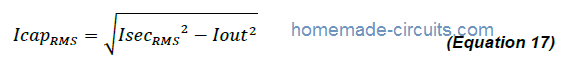 For a specified high switching frequency of the flyback, the maximum peak current from the secondary side of the transformer will generate a correspondingly high ripple voltage, imposed across the equivalent ESR of the output capacitor.
Considering this it must be ensured that the ESRmax rating of the capacitor does not exceed the specified acceptable ripple current capability of the capacitor.
The final design may fundamentally include the desired voltage rating, and ripple current capability of the capacitor, based on the actual ratio of the selected output voltage and current of the flyback.
For a specified high switching frequency of the flyback, the maximum peak current from the secondary side of the transformer will generate a correspondingly high ripple voltage, imposed across the equivalent ESR of the output capacitor.
Considering this it must be ensured that the ESRmax rating of the capacitor does not exceed the specified acceptable ripple current capability of the capacitor.
The final design may fundamentally include the desired voltage rating, and ripple current capability of the capacitor, based on the actual ratio of the selected output voltage and current of the flyback.
 Make sure that the ESR value is determined from the datasheet based on the frequency higher than 1kHz, which may be typically assumed to be between 10kHz to 100kHz.
It would be interesting to note that a solitary capacitor with a low ESR spec may be enough to control the output ripple.
You can try to include a small LC filter for higher peak currents, especially if the flyback is designed to work with a DCM mode, which might guarantee a reasonably good ripple voltage control at the output.
Step12
Further Important Considerations:
Make sure that the ESR value is determined from the datasheet based on the frequency higher than 1kHz, which may be typically assumed to be between 10kHz to 100kHz.
It would be interesting to note that a solitary capacitor with a low ESR spec may be enough to control the output ripple.
You can try to include a small LC filter for higher peak currents, especially if the flyback is designed to work with a DCM mode, which might guarantee a reasonably good ripple voltage control at the output.
Step12
Further Important Considerations:
 It can be done through the above equation.
In this formula PF stands for power factor of the power supply, we can apply 0.5 in case a proper reference becomes out of reach.
For the bridge rectifier select the diodes or the module having a forward amp rating 2 times more than the IACRMS.
For the voltage rating, it could be selected at 600V for a maximum 400V AC input specification.
It can be done through the above equation.
In this formula PF stands for power factor of the power supply, we can apply 0.5 in case a proper reference becomes out of reach.
For the bridge rectifier select the diodes or the module having a forward amp rating 2 times more than the IACRMS.
For the voltage rating, it could be selected at 600V for a maximum 400V AC input specification.

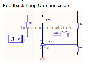 As indicated the above figure a straightforward RC (Rcomp, Ccomp) mostly becomes just enough to maintain good stability across the loop.
In general Rcomp value may be selected anything between 1K and 20K, while Ccomp could be within the range of 100nF and 470pF.
This concludes our elaborate discussion on how to design and calculate a flyback converter, if you have any suggestions or questions, you can put them forth in the following comment box, your questions will be replied ASAP.
Courtesy: Infineon
As indicated the above figure a straightforward RC (Rcomp, Ccomp) mostly becomes just enough to maintain good stability across the loop.
In general Rcomp value may be selected anything between 1K and 20K, while Ccomp could be within the range of 100nF and 470pF.
This concludes our elaborate discussion on how to design and calculate a flyback converter, if you have any suggestions or questions, you can put them forth in the following comment box, your questions will be replied ASAP.
Courtesy: Infineon

 NOTE: Please connect the 1k resistor of the opto LED to ground, which is mistakenly shown connected to positive.
The requested design for a buzzer circuit with progressive or an incrementing beep rate can be basically implemented through a voltage to frequency converter circuit
Although you may find many variants of voltage to frequency converter circuits, these may not be entirely easy to build due to their fairly complex design or due to the inclusion of unpopular, obsolete IC in it.
An alternative easier way of achieving this function could be by modifying an existing IC 4060 astable circuit with a homemade LED/LDR optocoupler as shown above.
As can be seen in the diagram, the LED/LDR opto is triggered through a slow rising voltage across its LED leads, which in turn induces a correspondingly slow decreasing resistance on the attached LDR.
The slow decreasing resistance of the LDR causes the timing capacitor of the astable to charge at proportionately faster rate, which subsequently causes a proportionately progressing or augmenting frequency rate at the output of the IC 4060.
P1 is for fine tuning the timing delay between the progressive beeps, possibly this component could be completely eliminated.
C1 can be also tweaked for adjusting the delay period between the beeps in order to make them faster or slower as per the application requirement.
The indicated buzzer unit here may be procured readymade in the form of a piezo buzzer or this can be also built at home by following this simple buzzer circuit guide.
Update:
Another interesting way of implementing a progressive buzzer beeper circuit could be by using a IC 555 monostable circuit and apply a slow rising voltage at its pin#5 control input....will update the circuit soon here.
NOTE: Please connect the 1k resistor of the opto LED to ground, which is mistakenly shown connected to positive.
The requested design for a buzzer circuit with progressive or an incrementing beep rate can be basically implemented through a voltage to frequency converter circuit
Although you may find many variants of voltage to frequency converter circuits, these may not be entirely easy to build due to their fairly complex design or due to the inclusion of unpopular, obsolete IC in it.
An alternative easier way of achieving this function could be by modifying an existing IC 4060 astable circuit with a homemade LED/LDR optocoupler as shown above.
As can be seen in the diagram, the LED/LDR opto is triggered through a slow rising voltage across its LED leads, which in turn induces a correspondingly slow decreasing resistance on the attached LDR.
The slow decreasing resistance of the LDR causes the timing capacitor of the astable to charge at proportionately faster rate, which subsequently causes a proportionately progressing or augmenting frequency rate at the output of the IC 4060.
P1 is for fine tuning the timing delay between the progressive beeps, possibly this component could be completely eliminated.
C1 can be also tweaked for adjusting the delay period between the beeps in order to make them faster or slower as per the application requirement.
The indicated buzzer unit here may be procured readymade in the form of a piezo buzzer or this can be also built at home by following this simple buzzer circuit guide.
Update:
Another interesting way of implementing a progressive buzzer beeper circuit could be by using a IC 555 monostable circuit and apply a slow rising voltage at its pin#5 control input....will update the circuit soon here.
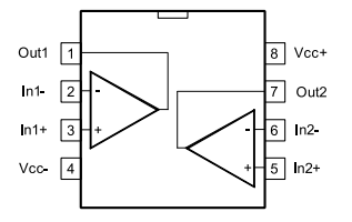 LM358 PINOUT DETAILS
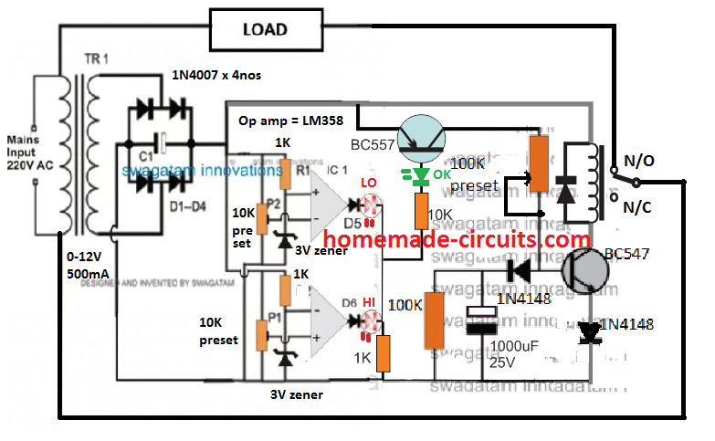

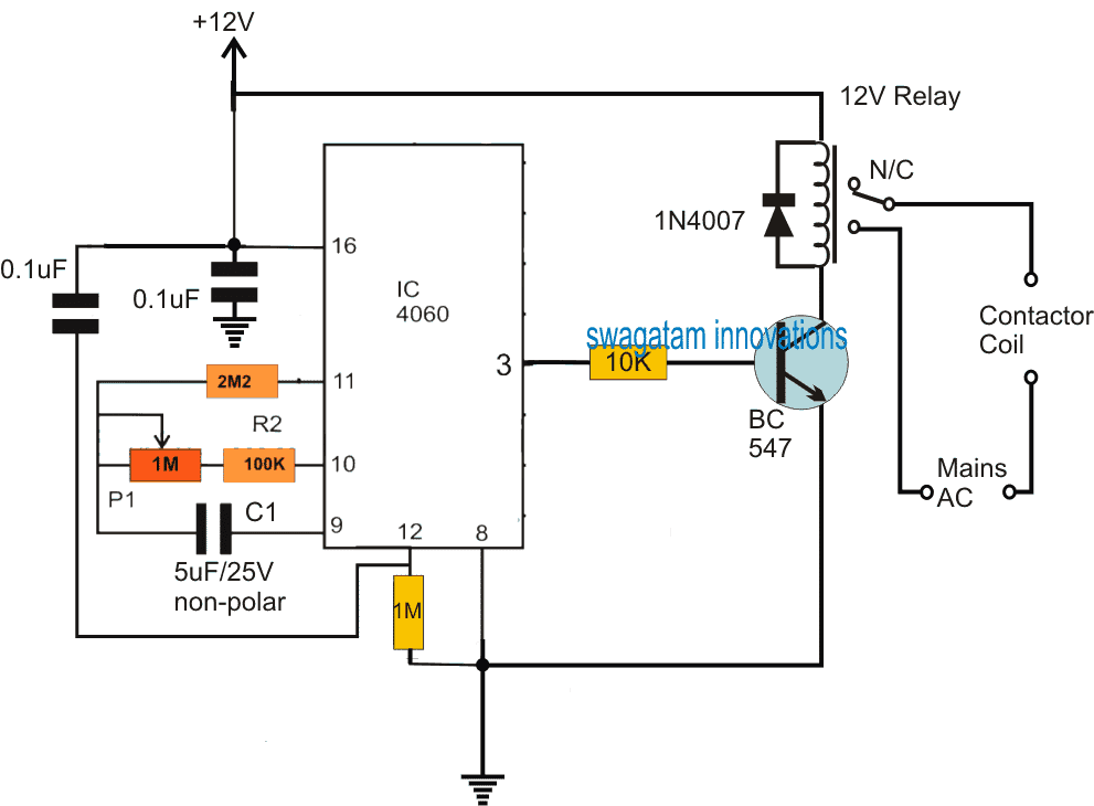 As may be seen in the above diagram, the IC 4060 is wired as a simple timer circuit whose timing limit is determined by the combined values of C1 and of P1/R1.
P1 can be adjusted for getting any desired delay ON/OFF at pin#3 of the IC, within a stipulated range.
Since the IC is configured as a free running astable multivibrator, the ON/OFF delays at the output pin#3 continues to toggle the transistor driver stage and the relay infinitely as long as power is available to the circuit.
If as per the specifications, P1 is adjusted to obtain a 1 hour ON/OFF delay at pin#3, the relay could be expected to switch ON/OFF at the same rate continuously as long as the circuit may remain powered.
The relay contacts can be seen wired with the 3 phase motor's contactor coil, which correspondingly operates at an identical delay rate during the course of ON/OFF switching.
This results in the switch ON and OFF of the borewell motor at a precise interval of 1 hour, which in turn makes sure that the ground water gets ample time to replenish and enable a sustained water supply for the motor to pump in.
Other time delays may be achieved for the proposed submersible pumpset timer circuit by appropriately adjusting P1, as per the given specifications or the ground water conditions.
As may be seen in the above diagram, the IC 4060 is wired as a simple timer circuit whose timing limit is determined by the combined values of C1 and of P1/R1.
P1 can be adjusted for getting any desired delay ON/OFF at pin#3 of the IC, within a stipulated range.
Since the IC is configured as a free running astable multivibrator, the ON/OFF delays at the output pin#3 continues to toggle the transistor driver stage and the relay infinitely as long as power is available to the circuit.
If as per the specifications, P1 is adjusted to obtain a 1 hour ON/OFF delay at pin#3, the relay could be expected to switch ON/OFF at the same rate continuously as long as the circuit may remain powered.
The relay contacts can be seen wired with the 3 phase motor's contactor coil, which correspondingly operates at an identical delay rate during the course of ON/OFF switching.
This results in the switch ON and OFF of the borewell motor at a precise interval of 1 hour, which in turn makes sure that the ground water gets ample time to replenish and enable a sustained water supply for the motor to pump in.
Other time delays may be achieved for the proposed submersible pumpset timer circuit by appropriately adjusting P1, as per the given specifications or the ground water conditions.
 The Delay Output from IC 555 can be obtained by solving the following formulas:
On Time Output= 0.7(R1 + R2)C
The Delay Output from IC 555 can be obtained by solving the following formulas:
On Time Output= 0.7(R1 + R2)C
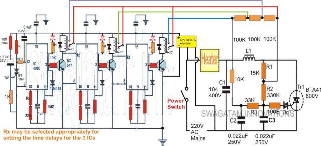 Referring to the above circuit design, the design is basically built around three identical IC 4060 timer stages and a standard light dimmer circuit enhanced with a high power triac for supporting the specified 17 amp kiln heater coil.
The entire kiln timer controller circuit can eb understood from the followng points:
The extreme left side IC 4060 timer circuit has all the component details which needs to be exactly replicated for the subsequent cascaded stages as these stages are identical with their componets and working specs.
These stages are rigged to produce sequential timing outputs and activating the relevant relays in response to the set individual timings.
When the indicated power switch is pressed, the SCR at extreme left latches and grounds the pin#12 of the IC enabling it to initiate the counting process.
During this period its pin#3 is held at logic low ensuring that the attached BC547 and the relay stay switched OFF.
Also since the pin#12 of the second and the third IC are rendered at the positive supply level, these ICs stay disabled while the first IC is activated and counting.
As soon as the set time delay elapses, pin#3 of the left most IC goes high, activating the concerned relay and also latching the pin#3 high situation via the 1N4148 diode connected with pin#11.
The above activation causes the pin#12 of the second C to get grounded via the BC547 collector, which in turn enables the second IC 4060 now begins counting, and the process is repeated identically activating the second relay after the set elapsed delay.
The third IC and the relay follows the same pattern sequentially.
The relay contacts can be seen connected with 3 series 100k resistors which become the part of the triac dimmer circuit, and the total value of these resistors determine the conduction level of the triac which in turn decide the heat level of the attached heater coil.
Initially while the first IC 4060 is counting, all the three resistor become involved in series allowing the lower preheat process to begin.
When the first relay activates it shorts one of the 100K resistors causing higher conduction through the triac and higher current to flow through the heater, raising the temperature of the kiln proportionately to a higher level, this is repeated by the second relay also, elevating the kiln temperature a little more, ....until the final relay clicks causing the kiln temperature to soar to the required 560 degrees.
If you have any more queries regarding the discussed kiln temperature timer controller circuit, please feel free to jot them in through comments.
Referring to the above circuit design, the design is basically built around three identical IC 4060 timer stages and a standard light dimmer circuit enhanced with a high power triac for supporting the specified 17 amp kiln heater coil.
The entire kiln timer controller circuit can eb understood from the followng points:
The extreme left side IC 4060 timer circuit has all the component details which needs to be exactly replicated for the subsequent cascaded stages as these stages are identical with their componets and working specs.
These stages are rigged to produce sequential timing outputs and activating the relevant relays in response to the set individual timings.
When the indicated power switch is pressed, the SCR at extreme left latches and grounds the pin#12 of the IC enabling it to initiate the counting process.
During this period its pin#3 is held at logic low ensuring that the attached BC547 and the relay stay switched OFF.
Also since the pin#12 of the second and the third IC are rendered at the positive supply level, these ICs stay disabled while the first IC is activated and counting.
As soon as the set time delay elapses, pin#3 of the left most IC goes high, activating the concerned relay and also latching the pin#3 high situation via the 1N4148 diode connected with pin#11.
The above activation causes the pin#12 of the second C to get grounded via the BC547 collector, which in turn enables the second IC 4060 now begins counting, and the process is repeated identically activating the second relay after the set elapsed delay.
The third IC and the relay follows the same pattern sequentially.
The relay contacts can be seen connected with 3 series 100k resistors which become the part of the triac dimmer circuit, and the total value of these resistors determine the conduction level of the triac which in turn decide the heat level of the attached heater coil.
Initially while the first IC 4060 is counting, all the three resistor become involved in series allowing the lower preheat process to begin.
When the first relay activates it shorts one of the 100K resistors causing higher conduction through the triac and higher current to flow through the heater, raising the temperature of the kiln proportionately to a higher level, this is repeated by the second relay also, elevating the kiln temperature a little more, ....until the final relay clicks causing the kiln temperature to soar to the required 560 degrees.
If you have any more queries regarding the discussed kiln temperature timer controller circuit, please feel free to jot them in through comments.
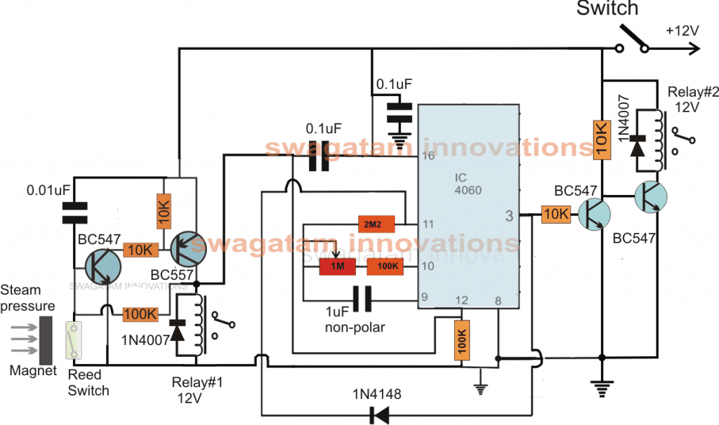
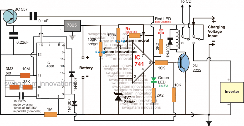 Note: The IC741 should be rated at above 24V...or replace it with LM321 IC

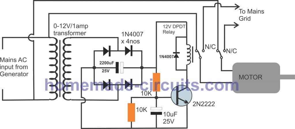
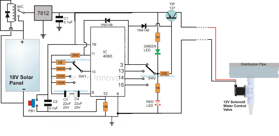 The IC 4060 can be seen configured in its standard timer/oscillator mode.
Pin#10 and pin#9 are associated with the time delay setting for the output pinouts 3, 13, 14 and 15.
The SW1 switch facilitates the time delay selection through the respective resistors which decides for how long the output of the IC may be rendered active, ensuring that the connected solenoid valve stays switched ON and in a water supplying mode only during this period of time.
The indicated timing resistors for SW1 are arbitrarily arranged and must be appropriately calculated during the actual implementation as per the crop specifications, and water availability.
SW1 is specified for a 4 position selection which can be increased to more positions by simply using a switch with more number of contacts and by adding subsequent number of resistors in the appropriate order.
SW2 is also a rotary switch identical to SW1 and is positioned for selecting the switching mode of the solenoid valve.
Pin#3 provides a continuous ON mode for the valve for the selected time slot after which the valve is switched off until the next day, whereas pin13, 14, 15 provides an oscillating (ON/OFF/ON/OFF) activation mode for the solenoid so that the water is managed in a more controlled manner, however this may be optional if the valve nozzle is correctly dimensioned for a restricted flow as per the given criteria.
The IC 4060 can be seen configured in its standard timer/oscillator mode.
Pin#10 and pin#9 are associated with the time delay setting for the output pinouts 3, 13, 14 and 15.
The SW1 switch facilitates the time delay selection through the respective resistors which decides for how long the output of the IC may be rendered active, ensuring that the connected solenoid valve stays switched ON and in a water supplying mode only during this period of time.
The indicated timing resistors for SW1 are arbitrarily arranged and must be appropriately calculated during the actual implementation as per the crop specifications, and water availability.
SW1 is specified for a 4 position selection which can be increased to more positions by simply using a switch with more number of contacts and by adding subsequent number of resistors in the appropriate order.
SW2 is also a rotary switch identical to SW1 and is positioned for selecting the switching mode of the solenoid valve.
Pin#3 provides a continuous ON mode for the valve for the selected time slot after which the valve is switched off until the next day, whereas pin13, 14, 15 provides an oscillating (ON/OFF/ON/OFF) activation mode for the solenoid so that the water is managed in a more controlled manner, however this may be optional if the valve nozzle is correctly dimensioned for a restricted flow as per the given criteria.

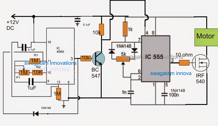
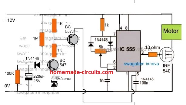
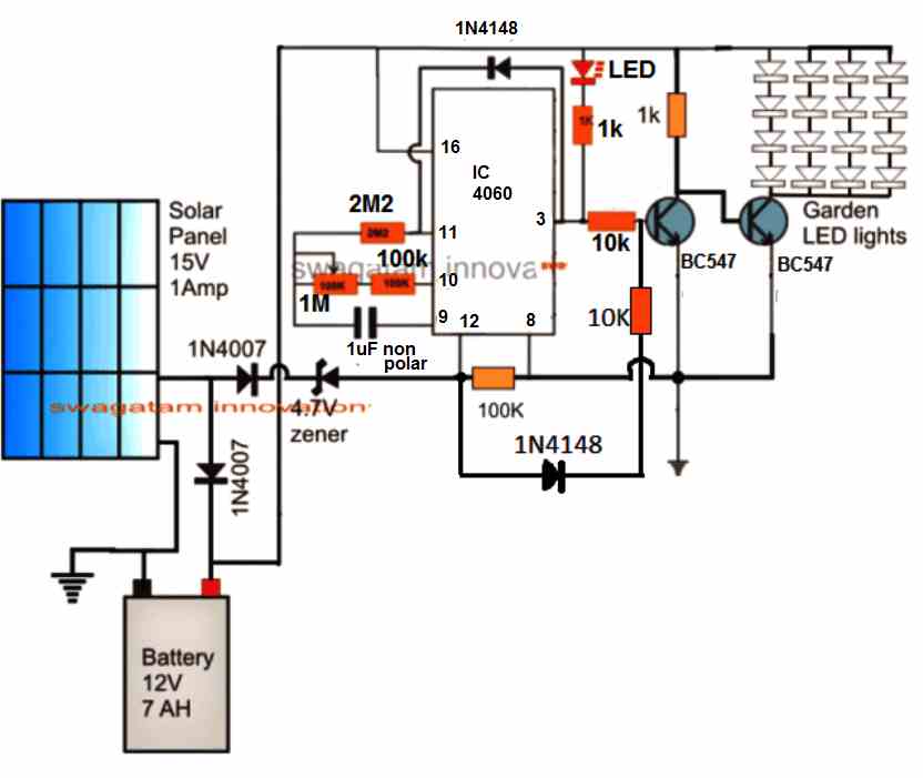
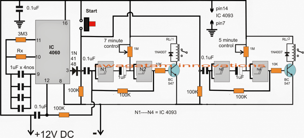
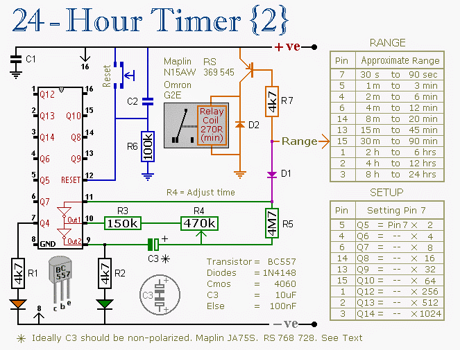
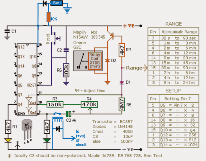 The sections which are colored in blue are the inserted modifications, we can see a battery backup being added at pin16 of the IC via diodes, and a relay at pin9 of the IC.
Since the capacitor C3 is responsible for initiating the counting process of the timer while it gets fully charged, this component could be targeted for the intended pausing/resuming of the timer.
As may be seen in the diagram, this is simply implemented by connecting C3 to the "hot" pin9 of the IC via a pair of relay contacts (N/O to be precise).
However for making the above implementation work, the IC needs to be supplied with its fundamental operating current and voltage while the mains is not available.
This is done by adding a battery back up to the IC via isolating diodes at pin16 of the IC.
The associated 10K resistor makes sure that the battery keeps getting the required trickle charge as long as the mains continues to be present.
When power is first switched ON, the relay at pin9 activates and connects C3 in the line so that the IC is able to initiate normally and begin its counting process.
The sections which are colored in blue are the inserted modifications, we can see a battery backup being added at pin16 of the IC via diodes, and a relay at pin9 of the IC.
Since the capacitor C3 is responsible for initiating the counting process of the timer while it gets fully charged, this component could be targeted for the intended pausing/resuming of the timer.
As may be seen in the diagram, this is simply implemented by connecting C3 to the "hot" pin9 of the IC via a pair of relay contacts (N/O to be precise).
However for making the above implementation work, the IC needs to be supplied with its fundamental operating current and voltage while the mains is not available.
This is done by adding a battery back up to the IC via isolating diodes at pin16 of the IC.
The associated 10K resistor makes sure that the battery keeps getting the required trickle charge as long as the mains continues to be present.
When power is first switched ON, the relay at pin9 activates and connects C3 in the line so that the IC is able to initiate normally and begin its counting process.
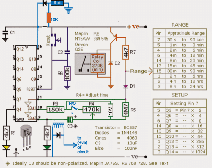
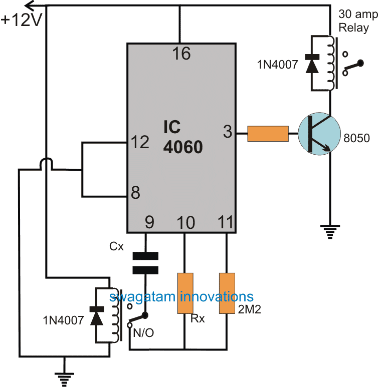 The design is nothing but a simple IC 4060 timer circuit.
The Cx, and Rx form its timing components, meaning altering the values of these proportionately alters the output frequency timing at pin#3 of the IC.
A low current relay can be seen attached with the timing capacitor of the IC whose contacts keep the capacitor connected with the circuit configuration during normal operations or when mains power is available.
However in the absence of mains, this relay quickly cuts off the capacitor from the circuit.
Since the charge content inside the capacitor fundamentally determines the time delay periods across the outputs of the IC, disconnecting the capacitor enables freezing of the charge content inside the capacitor intact until the power arrives back.
As soon as power gets restored the IC reads and responds to the available charge inside the capacitor and initiates the counting from the same period onward where it had stopped.
This system ensures that the IC resumes from the point where it was stopped due to the mains interruption.
The output pin#3 of the timer is connected with a 30 amp relay stage which may be configured with the contactor unit, for the necessary triggering of the pump and for watering the farm at the specified time intervals.
The timer circuit is designed to cycle ON/OFF with time delays as set by the values of the Cx and Rx, which may be calculated using the formula presented in this simple 4060 timer circuit article:
The design is nothing but a simple IC 4060 timer circuit.
The Cx, and Rx form its timing components, meaning altering the values of these proportionately alters the output frequency timing at pin#3 of the IC.
A low current relay can be seen attached with the timing capacitor of the IC whose contacts keep the capacitor connected with the circuit configuration during normal operations or when mains power is available.
However in the absence of mains, this relay quickly cuts off the capacitor from the circuit.
Since the charge content inside the capacitor fundamentally determines the time delay periods across the outputs of the IC, disconnecting the capacitor enables freezing of the charge content inside the capacitor intact until the power arrives back.
As soon as power gets restored the IC reads and responds to the available charge inside the capacitor and initiates the counting from the same period onward where it had stopped.
This system ensures that the IC resumes from the point where it was stopped due to the mains interruption.
The output pin#3 of the timer is connected with a 30 amp relay stage which may be configured with the contactor unit, for the necessary triggering of the pump and for watering the farm at the specified time intervals.
The timer circuit is designed to cycle ON/OFF with time delays as set by the values of the Cx and Rx, which may be calculated using the formula presented in this simple 4060 timer circuit article:
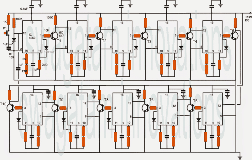 The above configuration takes care of the required programmable timing control, however for obtaining correspondingly sequencing time-scaled temperature control, we need a circuit that would be able to produce precise, adjustable temperature outputs.
For this we employ the following configuration in conjunction with the above circuit.
The above configuration takes care of the required programmable timing control, however for obtaining correspondingly sequencing time-scaled temperature control, we need a circuit that would be able to produce precise, adjustable temperature outputs.
For this we employ the following configuration in conjunction with the above circuit.
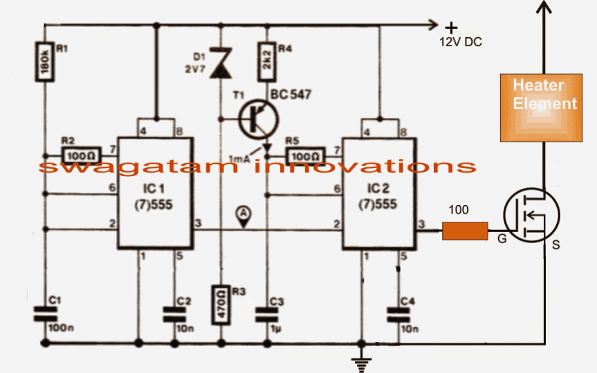 The link between this PWM stage and the above sequential timer stage is determined by an intermediate stage made by configuring a common collector NPN device along with a PNP inverter stage, which may be seen in the diagram below:
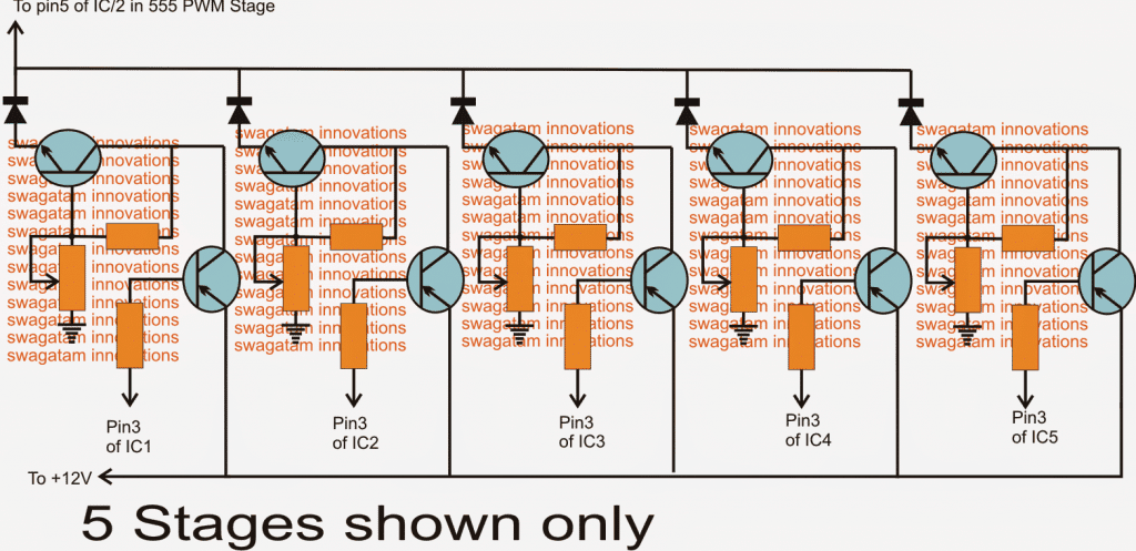 Five stages are shown in the diagram which may be increased to 10 numbers for integrating with the 10 stages of the first sequential timer circuit.
Each of the above shown stages consists of an NPN device wired up in a common collector mode for enabling a predetermined magnitude of voltage to be obtained at their emitters, which would depend upon the setting of the base preset or pot.
All the emitters are terminated to pin5 of the PWM IC2 via separate diodes.
The PNP devices work like inverters for inverting the counting low logic at pin3s of the sequential timer stages into a 12V supply for each of the common collector stages.
The pots here may be adjusted for feeding the preset amount of voltages to the PWM stage which in turn will regulate the PWMs to the mosfet and the heater device, generating the relevant amount of heat for that particular time slot.
Thus in response to the relevant timer stage switching, the corresponding common collector NPN gets activated producing the set amount of voltage at the pin5 of IC2 of the PWM circuit.
Depending upon this preset voltage the heater outputs gets regulated via the mosfet switching.
As the timer sequences, the heater temperature is switched to the next predetermined level as set by the base presets of the above common collector stages.
All resistors in the common collector circuit are 10k, the preset are also 10k, the NPNs are BC547 while the PNPs are BC557
Five stages are shown in the diagram which may be increased to 10 numbers for integrating with the 10 stages of the first sequential timer circuit.
Each of the above shown stages consists of an NPN device wired up in a common collector mode for enabling a predetermined magnitude of voltage to be obtained at their emitters, which would depend upon the setting of the base preset or pot.
All the emitters are terminated to pin5 of the PWM IC2 via separate diodes.
The PNP devices work like inverters for inverting the counting low logic at pin3s of the sequential timer stages into a 12V supply for each of the common collector stages.
The pots here may be adjusted for feeding the preset amount of voltages to the PWM stage which in turn will regulate the PWMs to the mosfet and the heater device, generating the relevant amount of heat for that particular time slot.
Thus in response to the relevant timer stage switching, the corresponding common collector NPN gets activated producing the set amount of voltage at the pin5 of IC2 of the PWM circuit.
Depending upon this preset voltage the heater outputs gets regulated via the mosfet switching.
As the timer sequences, the heater temperature is switched to the next predetermined level as set by the base presets of the above common collector stages.
All resistors in the common collector circuit are 10k, the preset are also 10k, the NPNs are BC547 while the PNPs are BC557

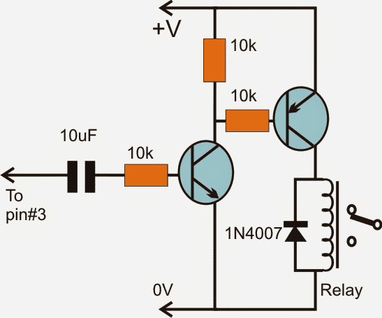
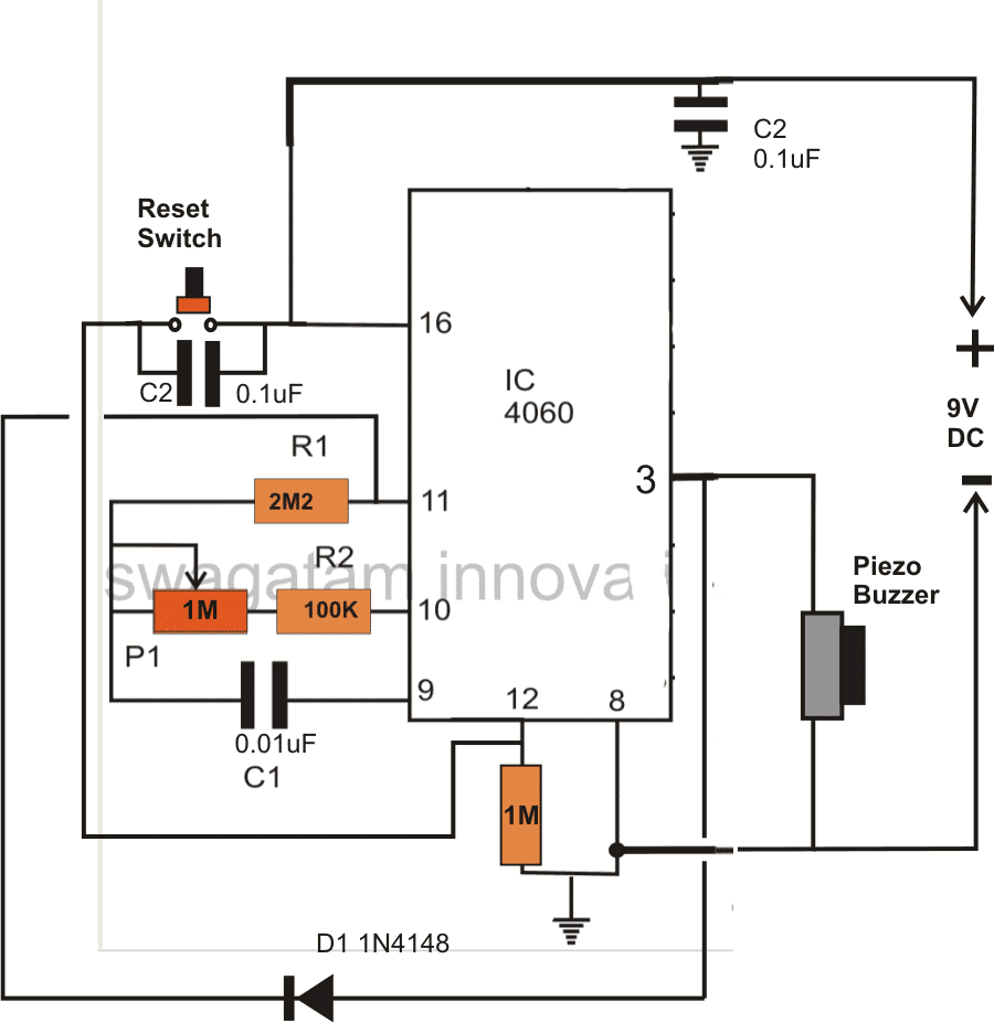
 Or Alternatively the following standard formula for calculating the Rt and Ct values is:
f(osc) = 1 / 2.3 x Rt x Ct
2.3 is a constant as per the ICs internal configuration.
Rt will in Ohms and Rt in Farads
Or Alternatively the following standard formula for calculating the Rt and Ct values is:
f(osc) = 1 / 2.3 x Rt x Ct
2.3 is a constant as per the ICs internal configuration.
Rt will in Ohms and Rt in Farads
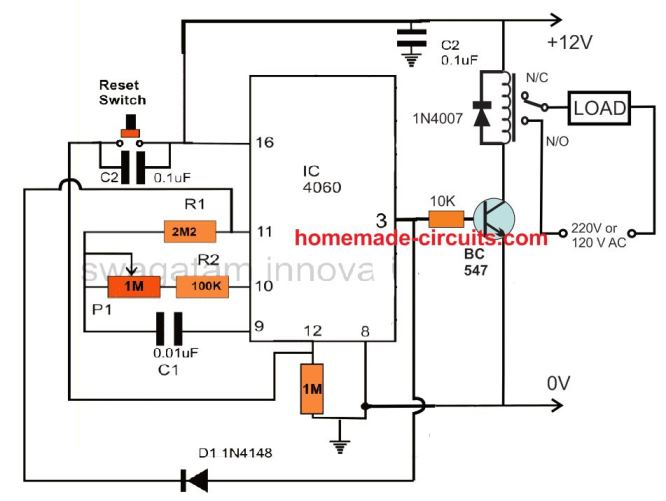 Remember the delay interval at pin3 can be increased by increasing the C1 value along with the P1 pot value.
Hoover, make sure that the C1 is always a non-polar, hence to increase its value you can connect many number non polar capacitors in parallel.
For example you can connect non-polar 1uF capacitor as many numbers as you want for getting a desired long delay.
Remember the delay interval at pin3 can be increased by increasing the C1 value along with the P1 pot value.
Hoover, make sure that the C1 is always a non-polar, hence to increase its value you can connect many number non polar capacitors in parallel.
For example you can connect non-polar 1uF capacitor as many numbers as you want for getting a desired long delay.
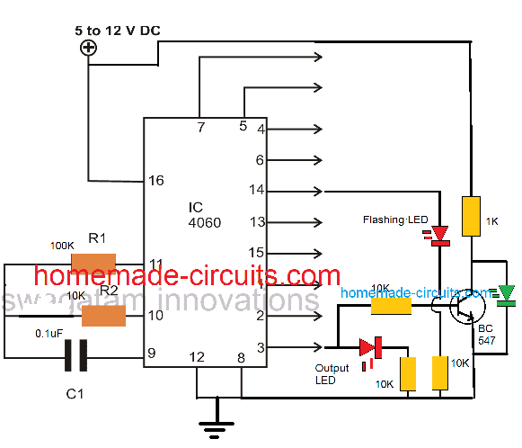 The following image shows how to latch IC 4060 output by adding a diode across the selected output pin and pin#11
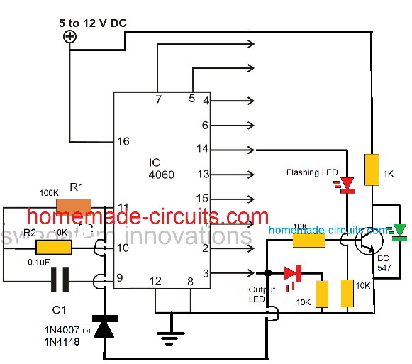 As we already know that the timing output or delay across all the shown output pins of the IC 4060 depends on the product of the values of R1 and C1, here pin#3 can be seen going after 32 logic pulses from pin#14 of the IC.
Meaning when the LED at pin#14 completes 32 pulses, the LED at pin#3 switches ON, and switches OFF after another 32 pulses from pin#14. Identically you may find different equivalent rates at the other output pins of the IC.
This timing proportion is observed when R2 and C1 are selected to be 10K and 0.1uF respectively.
As we already know that the timing output or delay across all the shown output pins of the IC 4060 depends on the product of the values of R1 and C1, here pin#3 can be seen going after 32 logic pulses from pin#14 of the IC.
Meaning when the LED at pin#14 completes 32 pulses, the LED at pin#3 switches ON, and switches OFF after another 32 pulses from pin#14. Identically you may find different equivalent rates at the other output pins of the IC.
This timing proportion is observed when R2 and C1 are selected to be 10K and 0.1uF respectively.
 Following 213 clocks, the counter output (Q14) goes high, turning on the oscillator across T1 and T2. By doing this a sharp 3 kHz frequency that is emitted through an 8 ohm small loudspeaker.
The circuit is powered down simply by turning off S1.
With the indicated R2 and C1, the buzzer will sound approximately An hour after the circuit has been started up.
By upgrading R2 with a 1 M adjustable potentiometer, the buzzer time period could be varied from 5 minutes to 214 hours.
The potentiometer scale may be appropriately calibrated for quick setting up.
The circuit utilizes hardly any current (0. 2 mA although the counter will be operating with 35 mA when the alarm signal is turned on) thus that a 9 V battery should promise quite an extended life.
Following 213 clocks, the counter output (Q14) goes high, turning on the oscillator across T1 and T2. By doing this a sharp 3 kHz frequency that is emitted through an 8 ohm small loudspeaker.
The circuit is powered down simply by turning off S1.
With the indicated R2 and C1, the buzzer will sound approximately An hour after the circuit has been started up.
By upgrading R2 with a 1 M adjustable potentiometer, the buzzer time period could be varied from 5 minutes to 214 hours.
The potentiometer scale may be appropriately calibrated for quick setting up.
The circuit utilizes hardly any current (0. 2 mA although the counter will be operating with 35 mA when the alarm signal is turned on) thus that a 9 V battery should promise quite an extended life.
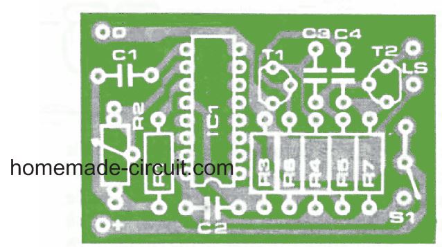
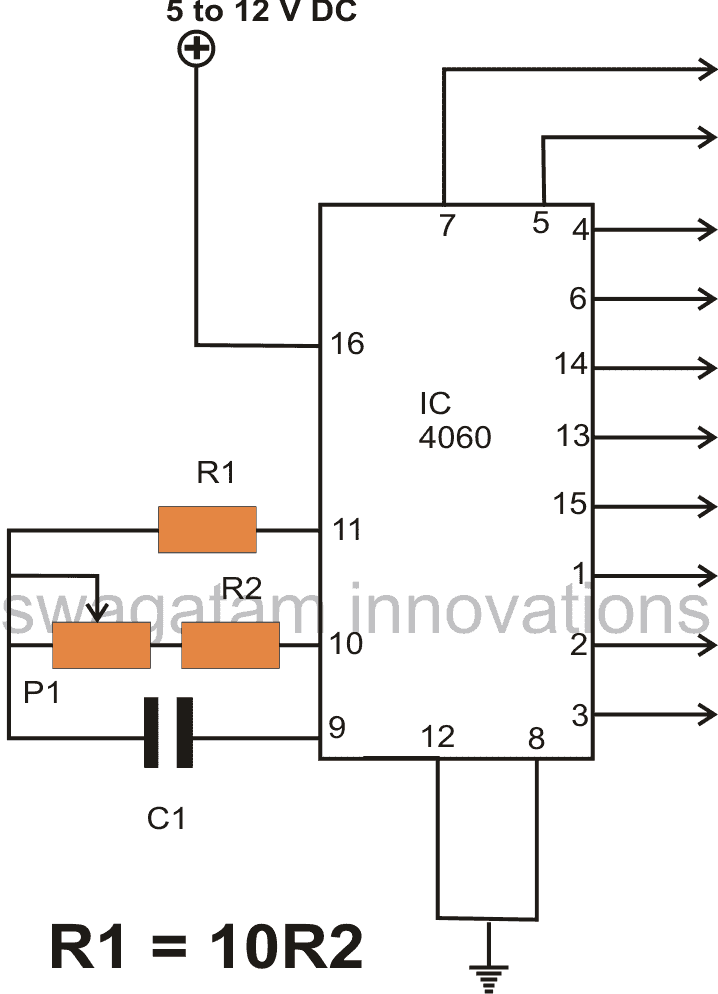 Test Circuit IC 4060
Parts List
R1 = 2M2
P1 = 1M pot
R2 = 100K
C1 = 1uF/25V
Test Circuit IC 4060
Parts List
R1 = 2M2
P1 = 1M pot
R2 = 100K
C1 = 1uF/25V
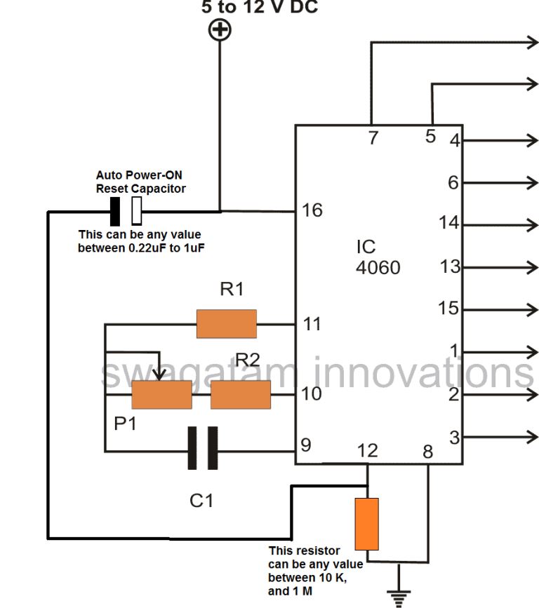 Enabling an automatic power switch ON resetting of a timer IC such as IC 4060 becomes crucial in order to initiate the IC clock, and counting process from zero.
If an auto reset facility is not included, the IC could exhibit a random or a haphazard initialization of its counting process, which may not be from the zero or start, rather from any intermediate level.
Therefore to ensure an automatic resetting for the IC, we must include an RC network with the reset pinout ofthe IC as explained below:
Instead of connecting the pin#12 directly to ground line, connect it through a high value resistor such as a 100K.
Then attach a small value capacitor from positive to pin#12, the value could be anywhere from 0.33uF to 1uF.
That's it, now your IC 4060 timer circuit is enabled with an auto reset feature, and will always initiate with a stable start, from zero.
Enabling an automatic power switch ON resetting of a timer IC such as IC 4060 becomes crucial in order to initiate the IC clock, and counting process from zero.
If an auto reset facility is not included, the IC could exhibit a random or a haphazard initialization of its counting process, which may not be from the zero or start, rather from any intermediate level.
Therefore to ensure an automatic resetting for the IC, we must include an RC network with the reset pinout ofthe IC as explained below:
Instead of connecting the pin#12 directly to ground line, connect it through a high value resistor such as a 100K.
Then attach a small value capacitor from positive to pin#12, the value could be anywhere from 0.33uF to 1uF.
That's it, now your IC 4060 timer circuit is enabled with an auto reset feature, and will always initiate with a stable start, from zero.
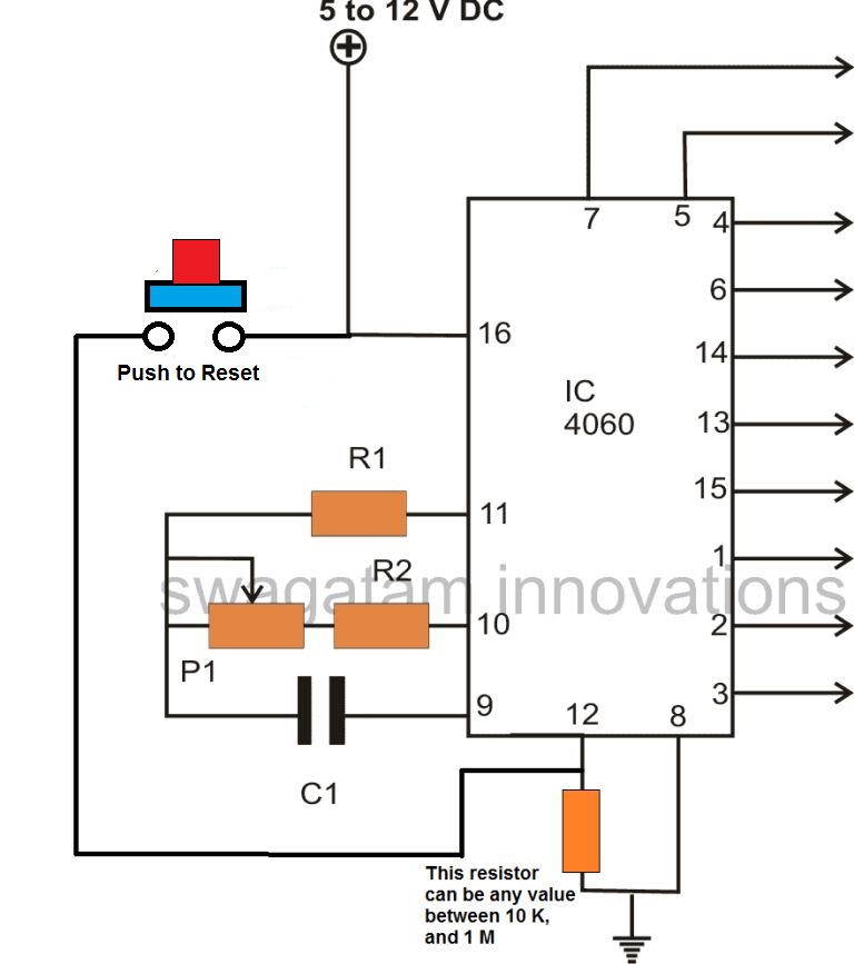 To achieve a manual resetting facility in any IC 4060 circuit, you can simply replace the capacitor with a push button, as shown above.
Pressing this button anytime during the counting process of the IC, will quickly reset the IC to zero, so that the counting can start afresh from zero.
To achieve a manual resetting facility in any IC 4060 circuit, you can simply replace the capacitor with a push button, as shown above.
Pressing this button anytime during the counting process of the IC, will quickly reset the IC to zero, so that the counting can start afresh from zero.
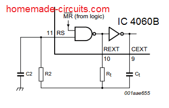 The standard formula for calculating the Rt and Ct values is:
f(osc) = 1 / 2.3 x Rt x Ct
2.3 is a constant as per the ICs internal configuration.
The oscillator will essentially work normally only when the selected values satisfy the conditions:
Rt << R2 and R2 x C2 << Rt x Ct.
R2 is positioned to reduce the frequency effect of the forward voltage over the input protection diodes.
C2 depicts the stray capacitance and is supposed to be minimal for enabling greater accuracy of the output time intervals.
For this, Ct must be relatively larger than C2, the larger the better.
Rt must be also a rather large value to negate the internal LOCMOS resistance, which appears in series with Rt internally.
Its typically value is around is 500�� at VDD = 5 V, 300�� at VDD = 10 V and 200�� at VDD = 15 V.
In order ensure a proper oscillatory action the most recommended values of the above mentioned timing parts must be configured as per the following conditions:
Ct�� 100 pF, up to any workable value,
10 k���� Rt�� 1 M��.
The standard formula for calculating the Rt and Ct values is:
f(osc) = 1 / 2.3 x Rt x Ct
2.3 is a constant as per the ICs internal configuration.
The oscillator will essentially work normally only when the selected values satisfy the conditions:
Rt << R2 and R2 x C2 << Rt x Ct.
R2 is positioned to reduce the frequency effect of the forward voltage over the input protection diodes.
C2 depicts the stray capacitance and is supposed to be minimal for enabling greater accuracy of the output time intervals.
For this, Ct must be relatively larger than C2, the larger the better.
Rt must be also a rather large value to negate the internal LOCMOS resistance, which appears in series with Rt internally.
Its typically value is around is 500�� at VDD = 5 V, 300�� at VDD = 10 V and 200�� at VDD = 15 V.
In order ensure a proper oscillatory action the most recommended values of the above mentioned timing parts must be configured as per the following conditions:
Ct�� 100 pF, up to any workable value,
10 k���� Rt�� 1 M��.
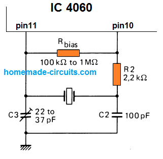 As we can see in the above figure, only the pin11 and pin10 are used for the integrating the crystal with the IC.
R2 is used for initiating the crystal oscillations by supplying the required voltage pulses to the crystal.
C3 and C2 enable the crystal to reach its rated resonance frequency.
C3 can be tweaked to change this resonance value of the crystal slightly, and therefore the output frequency of the IC 4060 accordingly.
As we can see in the above figure, only the pin11 and pin10 are used for the integrating the crystal with the IC.
R2 is used for initiating the crystal oscillations by supplying the required voltage pulses to the crystal.
C3 and C2 enable the crystal to reach its rated resonance frequency.
C3 can be tweaked to change this resonance value of the crystal slightly, and therefore the output frequency of the IC 4060 accordingly.
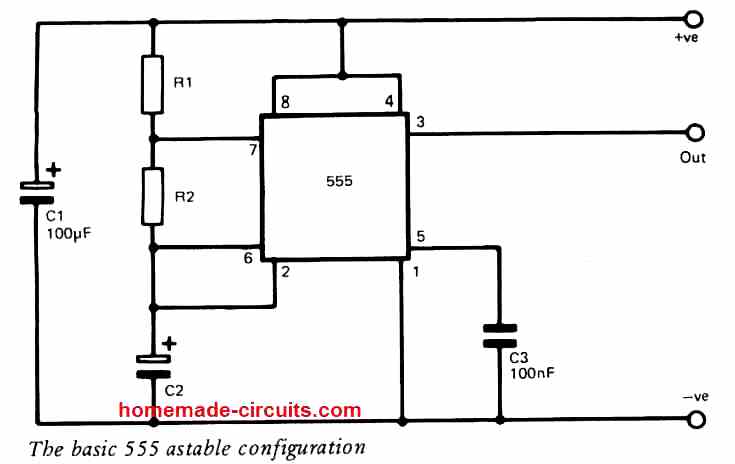 The design is actually a kind of relaxation oscillator where C2 is first allowed to charge to 2/3rd of the supply voltage via resistors R1 and R2, and then it is discharged by means of R2 to 1/3rd of the supply voltage.
The working frequency is thus determined through the values selected for resistors R1, R2 and the capacitor C2, which may be calculated using the formula:
Frequency = 1.44/(R1 + 2R2)C2
The reason for incorporating the R1 value twice the value of R2 (instead of simply using both values identical) is that R2 is used during both the charge and discharge paths of C2 and so it has two times more effect than R1. Common magnitudes for the timing parts will be 4k7 for R1 and R2, and 100nF for C2, which would provide an operating frequency of approximately 1kHz (4k7 + 2(4k7) = 14k1 x 100 nF = 0.00141, and 1.44 divided by 0.00141 = 1021Hz or 1.021kHz.
The operating frequency could be altered by modifying the value of the C2 capacitor.
Altering the value of C2 would produce an inversely proportional variation in frequency (for example if you double the C2 value will cause the frequency output to be halved and vice versa).
Likewise, the operating frequency could be modified by changing the value of the timing resistance which would again result in an inversely proportional results for the frequency of the astable circuit.
The design is actually a kind of relaxation oscillator where C2 is first allowed to charge to 2/3rd of the supply voltage via resistors R1 and R2, and then it is discharged by means of R2 to 1/3rd of the supply voltage.
The working frequency is thus determined through the values selected for resistors R1, R2 and the capacitor C2, which may be calculated using the formula:
Frequency = 1.44/(R1 + 2R2)C2
The reason for incorporating the R1 value twice the value of R2 (instead of simply using both values identical) is that R2 is used during both the charge and discharge paths of C2 and so it has two times more effect than R1. Common magnitudes for the timing parts will be 4k7 for R1 and R2, and 100nF for C2, which would provide an operating frequency of approximately 1kHz (4k7 + 2(4k7) = 14k1 x 100 nF = 0.00141, and 1.44 divided by 0.00141 = 1021Hz or 1.021kHz.
The operating frequency could be altered by modifying the value of the C2 capacitor.
Altering the value of C2 would produce an inversely proportional variation in frequency (for example if you double the C2 value will cause the frequency output to be halved and vice versa).
Likewise, the operating frequency could be modified by changing the value of the timing resistance which would again result in an inversely proportional results for the frequency of the astable circuit.
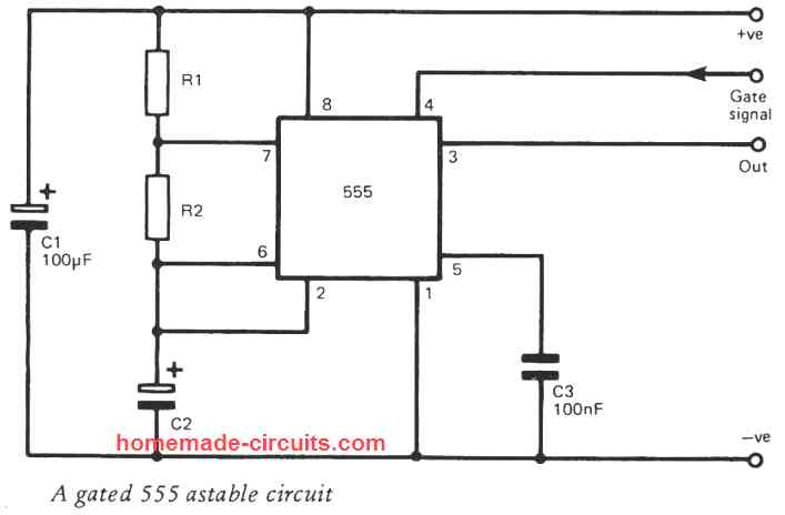 This configuration is essentially identical to the circuit demonstrated in the previous astable design, except the pin#4 of the IC 555 which here can be seen connected with the input gating signal, instead of the positive line.
It is required to pull the Pin#4 under around 0.5 volts to be able to shut off the 555 internal oscillator, which can force the output of the IC to go low as soon as the circuit is gated off.
If the pin#4 is left open or unconnected, the astable may keep oscillating anyway.
This configuration is essentially identical to the circuit demonstrated in the previous astable design, except the pin#4 of the IC 555 which here can be seen connected with the input gating signal, instead of the positive line.
It is required to pull the Pin#4 under around 0.5 volts to be able to shut off the 555 internal oscillator, which can force the output of the IC to go low as soon as the circuit is gated off.
If the pin#4 is left open or unconnected, the astable may keep oscillating anyway.
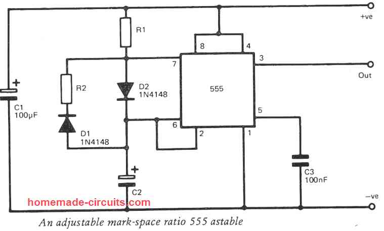 The circuit includes guiding diodes D1 and D2 which channelize the charging current for the timing capacitor through R1 and the discharge current through R2. This arrangement thus helps to generate a 1 : 1 mark-space ratio simply by selecting the R1 and R2 values perfectly identical.
lf the value of R1 is selected bigger than R2, causes the full charge time (output high) to be proportionately lengthier than the full discharge time (output low).
On the other hand, allowing R2 to be bigger in value than R1 causes the discharge time to be proportionately lengthier than the charge time.
The equations for determining the operating frequency and high output time are somewhat different because R2 is eliminated from the path while C2 is charging.
Hence while calculating the frequency the timing resistance is basically R1 + R2 and not R1 + 2R2 as in the standard astable formula for IC 555.
Likewise, while calculating the high output time, the timing resistance is only R2 and not R1 + R2. The involvement of the two diodes have practically no effect on the frequency, charge, and discharge times.
The circuit includes guiding diodes D1 and D2 which channelize the charging current for the timing capacitor through R1 and the discharge current through R2. This arrangement thus helps to generate a 1 : 1 mark-space ratio simply by selecting the R1 and R2 values perfectly identical.
lf the value of R1 is selected bigger than R2, causes the full charge time (output high) to be proportionately lengthier than the full discharge time (output low).
On the other hand, allowing R2 to be bigger in value than R1 causes the discharge time to be proportionately lengthier than the charge time.
The equations for determining the operating frequency and high output time are somewhat different because R2 is eliminated from the path while C2 is charging.
Hence while calculating the frequency the timing resistance is basically R1 + R2 and not R1 + 2R2 as in the standard astable formula for IC 555.
Likewise, while calculating the high output time, the timing resistance is only R2 and not R1 + R2. The involvement of the two diodes have practically no effect on the frequency, charge, and discharge times.
 This configuration is similar to the standard 555 astable setup except the pin#5 decoupling capacitor which can be seen missing and the control voltage injected to this pin#5. This control voltage pinout of the IC is internally linked with a resistive divider network that fixes the 2/3rd supply voltage threshold limit, enabling the IC 555 to flip from the charge mode to the discharge mode.
When pin#5 potential is pulled over 2/3rd of the supply voltage, causes the frequency of the IC 555 to reduce because C2 now has to charge to, and discharge from, a higher voltage level, which delays the ON/OFF process and makes it longer.
When pin#5 is applied with a potential below 2/3rd of the supply voltage, it causes a decrease in the charging/discharging voltage across C2. This allows both the frequency ON/OFF processes to consume less time, causing the operating frequency to increase.
However, there is no change in the output waveform at pin#3, but there may be a little change in the shape of the waveform and the amplitude of the signal across C2.
If we see the internal layout of the IC 555 we find that pin#5 is attached directly to the internal potential divider.
Due to this the threshold voltage where the IC switches from the charge state to the discharge state is not identical to the voltage introduced at pin#5. This condition restricts the amount of control which you can get through an external control voltage at pin#5 of the IC.
Due to this the output frequency drops by slightly more than 50% when the control voltage at pin#5 is made as high as the positive supply voltage.
The output frequency can be increased a bit higher than twice if the control pin#5 is held at 1/3rd of the supply voltage, and this could be enhanced even slightly more when pin#5 voltage is held a little bit lower.
On the other hand, if we pull the pin#5 potential extremely low, the IC could malfunction and you may find the output frequency reducing to a great level.
Hence, it is recommended to maintain the control voltage at pin#5 between 1/3rd of the supply voltage and the full supply voltage range.
This configuration is similar to the standard 555 astable setup except the pin#5 decoupling capacitor which can be seen missing and the control voltage injected to this pin#5. This control voltage pinout of the IC is internally linked with a resistive divider network that fixes the 2/3rd supply voltage threshold limit, enabling the IC 555 to flip from the charge mode to the discharge mode.
When pin#5 potential is pulled over 2/3rd of the supply voltage, causes the frequency of the IC 555 to reduce because C2 now has to charge to, and discharge from, a higher voltage level, which delays the ON/OFF process and makes it longer.
When pin#5 is applied with a potential below 2/3rd of the supply voltage, it causes a decrease in the charging/discharging voltage across C2. This allows both the frequency ON/OFF processes to consume less time, causing the operating frequency to increase.
However, there is no change in the output waveform at pin#3, but there may be a little change in the shape of the waveform and the amplitude of the signal across C2.
If we see the internal layout of the IC 555 we find that pin#5 is attached directly to the internal potential divider.
Due to this the threshold voltage where the IC switches from the charge state to the discharge state is not identical to the voltage introduced at pin#5. This condition restricts the amount of control which you can get through an external control voltage at pin#5 of the IC.
Due to this the output frequency drops by slightly more than 50% when the control voltage at pin#5 is made as high as the positive supply voltage.
The output frequency can be increased a bit higher than twice if the control pin#5 is held at 1/3rd of the supply voltage, and this could be enhanced even slightly more when pin#5 voltage is held a little bit lower.
On the other hand, if we pull the pin#5 potential extremely low, the IC could malfunction and you may find the output frequency reducing to a great level.
Hence, it is recommended to maintain the control voltage at pin#5 between 1/3rd of the supply voltage and the full supply voltage range.
 You can expect an output power of a few hundred milliwatts from the IC 555 astable output into any 8 ohm load or a loudspeaker.
However, you must be careful in such applications considering that several smaller loudspeakers are only able to handle a power input of 200 mW approximately.
Other than the normal implementations of the IC 555 astable as discussed in the previous paragraphs, it is easily possible to combine the various astable configurations explained thus far to offer (for example) a gated, frequency modulated tone generator, or a gated squarewave generator to create innovative IC 555 circuits.
Due to the great versatility and its affordable cost the IC 555 has been so far successful in becoming one of the most popular ICs among the hobbyists.
You can expect an output power of a few hundred milliwatts from the IC 555 astable output into any 8 ohm load or a loudspeaker.
However, you must be careful in such applications considering that several smaller loudspeakers are only able to handle a power input of 200 mW approximately.
Other than the normal implementations of the IC 555 astable as discussed in the previous paragraphs, it is easily possible to combine the various astable configurations explained thus far to offer (for example) a gated, frequency modulated tone generator, or a gated squarewave generator to create innovative IC 555 circuits.
Due to the great versatility and its affordable cost the IC 555 has been so far successful in becoming one of the most popular ICs among the hobbyists.
 Referring to the above 555 set-reset diagram, SW1 and SW2 are arranged as the limit switches for the start and the finish limits of the motor rotation.
Let's assume the motor is at the SW1 end, and the SW1 is pressed in the course of the action.
With SW1 pressed, the IC 555 activates and switches ON the transistor T1. The transistor T1 actuates the DPDT relay and flips the motor rotation to the opposite side.
However, the motor is unable to revert immediately, because pressing SW1 also activates a monostable timer, which disconnects the power to the above motor relay.
Referring to the above 555 set-reset diagram, SW1 and SW2 are arranged as the limit switches for the start and the finish limits of the motor rotation.
Let's assume the motor is at the SW1 end, and the SW1 is pressed in the course of the action.
With SW1 pressed, the IC 555 activates and switches ON the transistor T1. The transistor T1 actuates the DPDT relay and flips the motor rotation to the opposite side.
However, the motor is unable to revert immediately, because pressing SW1 also activates a monostable timer, which disconnects the power to the above motor relay.
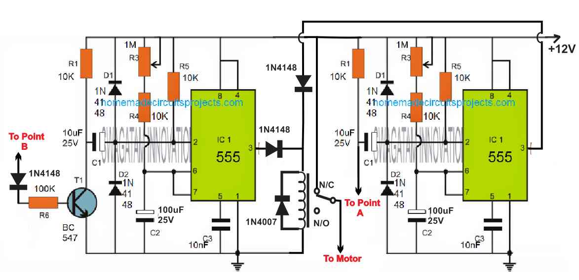 However, after about 2 seconds, or as per the set time of the monostable timer, the IC 555 switches OFF its pin3, causing the relay to return to its N/C point.
This instantly supplies the positive supply to the motor relay allowing the motor to start moving towards the opposite direction.
As soon as the moves starts moving, it releases the SW1, and when the motor reaches the other end of its rotational path, it presses the SW2 limit switch.
SW2 now resets the motor control circuit so that the motor can again rotate to the opposite direction.
However, just like the above case, SW2 also activates the second monostable timer on the left side, which causes the left side IC 555 to activate its pin3, which in turn causes the SPDT relay to disconnect the positive supply to the motor relay.
After about seconds the left side monostable's time lapses, switching Off its pin3 and the relay returns to its N/C point.
This instantly connects the positive supply to the motor relay and the motor now yet again starts rotating in the reverse direction towards the SW1 switch.
The above procedure keeps repeating, allowing the motor to move in the reverse forward direction, and enabling the motor mechanism to implement the tennis ball throwing action swiftly.
This concludes the explanation for the making of a tennis ball throwing machine circuit, if you have any related questions, do feel free to express them through the comment box.
However, after about 2 seconds, or as per the set time of the monostable timer, the IC 555 switches OFF its pin3, causing the relay to return to its N/C point.
This instantly supplies the positive supply to the motor relay allowing the motor to start moving towards the opposite direction.
As soon as the moves starts moving, it releases the SW1, and when the motor reaches the other end of its rotational path, it presses the SW2 limit switch.
SW2 now resets the motor control circuit so that the motor can again rotate to the opposite direction.
However, just like the above case, SW2 also activates the second monostable timer on the left side, which causes the left side IC 555 to activate its pin3, which in turn causes the SPDT relay to disconnect the positive supply to the motor relay.
After about seconds the left side monostable's time lapses, switching Off its pin3 and the relay returns to its N/C point.
This instantly connects the positive supply to the motor relay and the motor now yet again starts rotating in the reverse direction towards the SW1 switch.
The above procedure keeps repeating, allowing the motor to move in the reverse forward direction, and enabling the motor mechanism to implement the tennis ball throwing action swiftly.
This concludes the explanation for the making of a tennis ball throwing machine circuit, if you have any related questions, do feel free to express them through the comment box.
 The speaker can have any impedance value, due to the presence of the current limiting resistance Rx.
A safe value could be around 70 Ohms 1 watt.
For making a high power continuous tone alarm circuit we cam upgrade the above circuit through a power transistor driver Q1 and a more powerful loudspeaker, as shown below:
The speaker can have any impedance value, due to the presence of the current limiting resistance Rx.
A safe value could be around 70 Ohms 1 watt.
For making a high power continuous tone alarm circuit we cam upgrade the above circuit through a power transistor driver Q1 and a more powerful loudspeaker, as shown below:
 Since the design may produce a high level of ripple volatge, D1 and C3 are included to prevent the ripple interference with the IC 555 functioning.
Diodes D2 and D3 are included to neutralize the inductive switching spikes generated from the speaker coil, and to safeguard the transistor Q1 against damage.
Since the design may produce a high level of ripple volatge, D1 and C3 are included to prevent the ripple interference with the IC 555 functioning.
Diodes D2 and D3 are included to neutralize the inductive switching spikes generated from the speaker coil, and to safeguard the transistor Q1 against damage.
 We have already studied how pin 5 can be used for controlling the pulse width of the IC 555.
Here IC 2 is configured as a 1 Hz oscillator circuit which causes pin 5 of IC 1 to alternately become low at a 1 Hz rate.
This in turn causes pin 3 800 Hz pulse width to narrow to an extent which almost turns OFF Q1. This produces a 1Hz sharp pulsed alarm effect on the loudspeaker.
We have already studied how pin 5 can be used for controlling the pulse width of the IC 555.
Here IC 2 is configured as a 1 Hz oscillator circuit which causes pin 5 of IC 1 to alternately become low at a 1 Hz rate.
This in turn causes pin 3 800 Hz pulse width to narrow to an extent which almost turns OFF Q1. This produces a 1Hz sharp pulsed alarm effect on the loudspeaker.
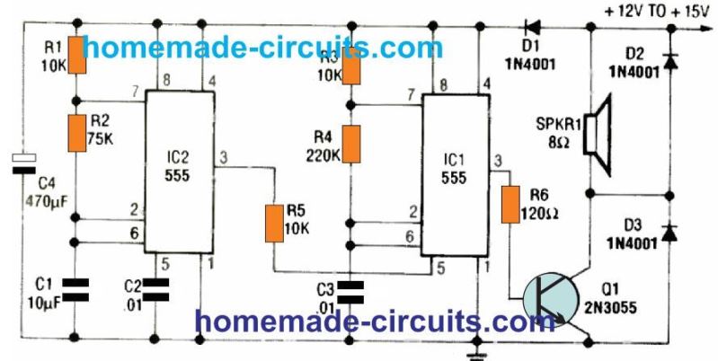 If you want to convert the previous design into an ear piercing warble alarm, you can do it by simply replacing the D1 diode with a 10 K resistor as revealed in the above diagram.
Also known as he-haw alarm, these are commonly used in European emergency vehicles.
We know that pin 5 can be used with an external high/low signal for modulating the pin 3 output with a corresponding widening/narrowing pulse widths.
The 1 Hz alternate high low supply at pin 5 of IC2 forces the output pin #3 voltage of IC 1 to generate a symmetrically changing frequency varying from 500 Hz to 440 Hz.
This causes the speaker to generate the required sharp high volume warble alarm sound at 1 Hz rate.
If you want to convert the previous design into an ear piercing warble alarm, you can do it by simply replacing the D1 diode with a 10 K resistor as revealed in the above diagram.
Also known as he-haw alarm, these are commonly used in European emergency vehicles.
We know that pin 5 can be used with an external high/low signal for modulating the pin 3 output with a corresponding widening/narrowing pulse widths.
The 1 Hz alternate high low supply at pin 5 of IC2 forces the output pin #3 voltage of IC 1 to generate a symmetrically changing frequency varying from 500 Hz to 440 Hz.
This causes the speaker to generate the required sharp high volume warble alarm sound at 1 Hz rate.
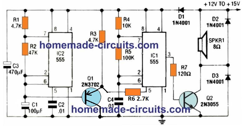 The IC 555 can be also used for making a perfectly imitating police siren circuit as demonstrated above.
The circuit is designed to produce the typical wailing sound commonly heard in police sirens.
Here IC2 is connected as a low frequency oscillator with a frequency set at a 6 second ON OFF rate.
The slow exponential triangle wave ramp generated across its C1 is fed at the base of Q1 configured as anemitter follower.
The frequency of IC1 is set at 500 Hz which becomes its center frequency.
The slow rising and falling ramp at base of Q1 follows at its emitter and modulates pin 5 of IC1. The slow ramp causes alternate cycles of slow rising voltage for 3 seconds, and slow decaying voltage for the 3 seconds on pin 5. Due to this pin 3 frequency and PWM also modulates accordingly generating the wailing police siren sound effect.
The IC 555 can be also used for making a perfectly imitating police siren circuit as demonstrated above.
The circuit is designed to produce the typical wailing sound commonly heard in police sirens.
Here IC2 is connected as a low frequency oscillator with a frequency set at a 6 second ON OFF rate.
The slow exponential triangle wave ramp generated across its C1 is fed at the base of Q1 configured as anemitter follower.
The frequency of IC1 is set at 500 Hz which becomes its center frequency.
The slow rising and falling ramp at base of Q1 follows at its emitter and modulates pin 5 of IC1. The slow ramp causes alternate cycles of slow rising voltage for 3 seconds, and slow decaying voltage for the 3 seconds on pin 5. Due to this pin 3 frequency and PWM also modulates accordingly generating the wailing police siren sound effect.
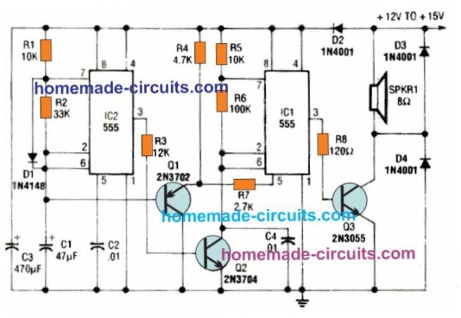 The final circuit in the list is another very interesting sound effect generator using the IC 555 astable.
It is the red-alert alarm sound generator, also called the star trek siren due to its frequent use in the popular TV series star trek.
Typically, the red alert alarm sound initiates with a low frequency tone, that rises to a high frequency note within a quick span of around 1.15 seconds, and cuts off for 0.35 seconds, and again rises from a low to high frequency, and the cycle continues giving rise to the star trek red-alert alarm sound.
Just like the previous alarm and siren sound circuits, this circuit also keeps repeating the sequence as long as it remains powered.
The IC 2 here is configured as a non symmetrical oscillator circuit.
The capacitor C1 is alternately charged through the elements R1 and D1, and is alternately discharged through R2.
This produces a quick rising and fading sawtooth pluses across the capacitor C1. This ramping signal is buffered by the emitter follower and applied as a modulating voltage to the control input pin 5 of IC1 via R7.
Due to the sawtooth nature this waveform causes the pin 3 output frequency of IC1 to gradually rise for the slow decaying portion of the waveform, and then quickly drops during the collapsing part of the waveform.
During each of the decaying section of the waveform cycle, the corresponding rectangular pulse from pin 3 of IC2 instantly switches OFF Q2, which in turn causes pin2 of IC2 to go low.
This interrupts the C2 output and the rising tone on the speaker, giving rise to the peculiar red alert star trek alarm sound effect.
The final circuit in the list is another very interesting sound effect generator using the IC 555 astable.
It is the red-alert alarm sound generator, also called the star trek siren due to its frequent use in the popular TV series star trek.
Typically, the red alert alarm sound initiates with a low frequency tone, that rises to a high frequency note within a quick span of around 1.15 seconds, and cuts off for 0.35 seconds, and again rises from a low to high frequency, and the cycle continues giving rise to the star trek red-alert alarm sound.
Just like the previous alarm and siren sound circuits, this circuit also keeps repeating the sequence as long as it remains powered.
The IC 2 here is configured as a non symmetrical oscillator circuit.
The capacitor C1 is alternately charged through the elements R1 and D1, and is alternately discharged through R2.
This produces a quick rising and fading sawtooth pluses across the capacitor C1. This ramping signal is buffered by the emitter follower and applied as a modulating voltage to the control input pin 5 of IC1 via R7.
Due to the sawtooth nature this waveform causes the pin 3 output frequency of IC1 to gradually rise for the slow decaying portion of the waveform, and then quickly drops during the collapsing part of the waveform.
During each of the decaying section of the waveform cycle, the corresponding rectangular pulse from pin 3 of IC2 instantly switches OFF Q2, which in turn causes pin2 of IC2 to go low.
This interrupts the C2 output and the rising tone on the speaker, giving rise to the peculiar red alert star trek alarm sound effect.
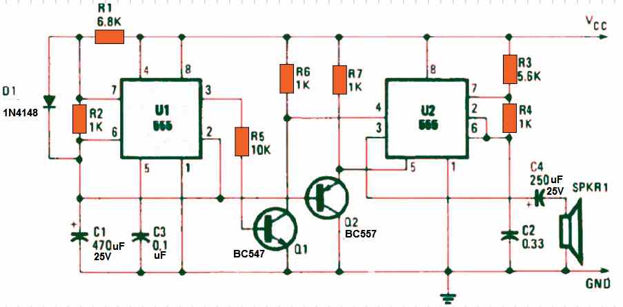 If you actually wish to draw attention of the folks, you can use an amplifier to boost the whooper sound effect.
IC U1 is hooked up as a low-frequency asymmetrical oscillator.
Q1 inverts the output signal and supplies it to the reset terminal of U2 at pin 4. IC 555 U2 is wired as an audio oscillator and starts operating as soon as the UI 555 output goes low.
Since the U2 pin 5 constant potential constant, the circuit might only create a "bleeping." sound.
The voltage over capacitor C is applied to the transistor Q2 base, switching it on, which grounds the pin 5 of U2 555. Once the pin4 reset signal frequency on pin 4 drops, causes the U2 output frequency to increase.
The of U2 555 then starts sounding like the "whoooop", which begins with low frequency tone, and gradually ends with a high ear piercing tone.
Back to You
Well these were some hints regarding how to use IC 555 for creating useful alarm and siren circuits.
Do you have any other interesting sound effect generator using IC 555? If you do, please provide the details here, we will be most happy to include it in the above list.
If you actually wish to draw attention of the folks, you can use an amplifier to boost the whooper sound effect.
IC U1 is hooked up as a low-frequency asymmetrical oscillator.
Q1 inverts the output signal and supplies it to the reset terminal of U2 at pin 4. IC 555 U2 is wired as an audio oscillator and starts operating as soon as the UI 555 output goes low.
Since the U2 pin 5 constant potential constant, the circuit might only create a "bleeping." sound.
The voltage over capacitor C is applied to the transistor Q2 base, switching it on, which grounds the pin 5 of U2 555. Once the pin4 reset signal frequency on pin 4 drops, causes the U2 output frequency to increase.
The of U2 555 then starts sounding like the "whoooop", which begins with low frequency tone, and gradually ends with a high ear piercing tone.
Back to You
Well these were some hints regarding how to use IC 555 for creating useful alarm and siren circuits.
Do you have any other interesting sound effect generator using IC 555? If you do, please provide the details here, we will be most happy to include it in the above list.
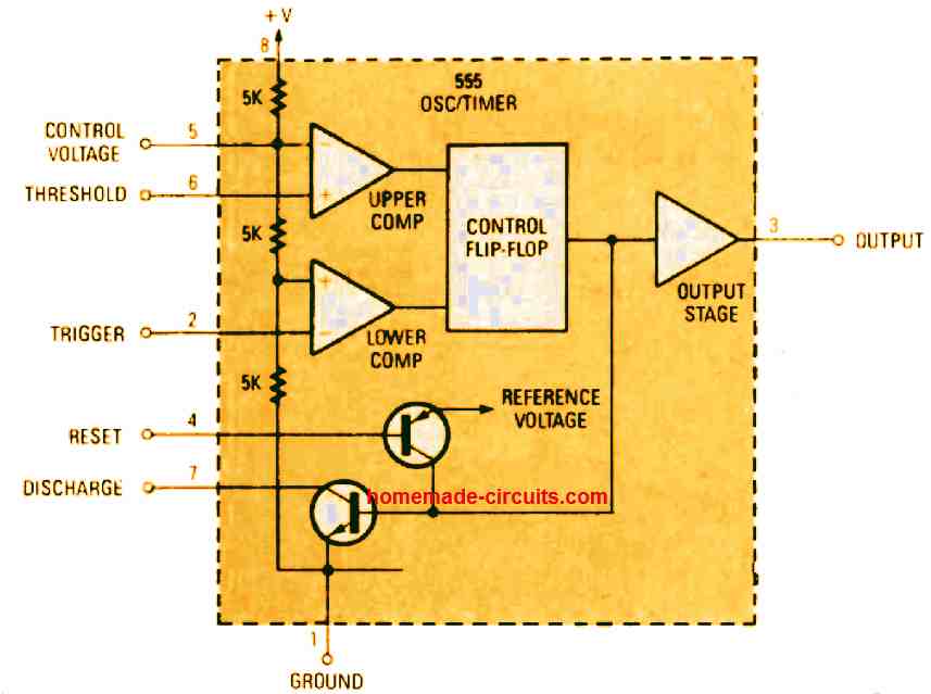
 In this mode when the IC is switched ON by briefly connecting pin 2 with the ground line, the output of the IC at pin 3 instantly becomes high, and this high continues to hold for a period of time as fixed by the values of the resistor and the capacitor in the RC network connected at pins 6 and 7.
The timing count could be quickly aborted by temporarily grounding the pin 4 of the IC.
When the circuit is powered ON, the circuit initiates with a low at the output pin 3, and the capacitor of the RC network stays in the discharged condition through pin 7 of the 555. As soon as a timing cycle is started by connecting pin2 to ground or the negative line C1 starts charging exponentially (via R1) towards the supply voltage level.
As soon as it gets to 2/3 voltage level of the supply, the IC 555 output pin3 becomes low yet again.
This creates a shorting effect across C1, forcing the capacitor to discharge, which completes and finishes a single timing cycle for the IC.
The timing interval for which the output of the IC remains low does not depend on the supply voltage simply because the C1 charging level, and therefore the voltage introduced to the threshold input pin 6 of the IC, are both directly proportional to the supply voltage.
The period of the time interval (T) can be expressed by the formula:
T= 1.1 x R1 x C1
Let's suppose R1 is selected to be a 1 megohm resistors and C1 is 1 uF, the output time for which the IC 555 output pin 3 would be low is: T =1.1 x 1,000,000 x .000,001= 1.1 seconds
The C1 value can be anywhere between 0.001uF to 100 ��F; and R1 could be any value between 1k ohms and 10 megohms.
It is advisable to have the capacitor C1 a low leakage type to guarantee improved timing accuracy.
As soon as the output of the 555 goes high due to a momentary ground signal at pin 2, applying further ground signal trigger pulses to pin 2 produces no effect on the output condition.
But, it may be possible to quickly abort the output ON time by applying a momentary ground or negative signal to pin 4 RESET pin of the IC.
The action forces the 555's internal flip -flop to get reset, causing the 555's output to revert to low.
In this mode when the IC is switched ON by briefly connecting pin 2 with the ground line, the output of the IC at pin 3 instantly becomes high, and this high continues to hold for a period of time as fixed by the values of the resistor and the capacitor in the RC network connected at pins 6 and 7.
The timing count could be quickly aborted by temporarily grounding the pin 4 of the IC.
When the circuit is powered ON, the circuit initiates with a low at the output pin 3, and the capacitor of the RC network stays in the discharged condition through pin 7 of the 555. As soon as a timing cycle is started by connecting pin2 to ground or the negative line C1 starts charging exponentially (via R1) towards the supply voltage level.
As soon as it gets to 2/3 voltage level of the supply, the IC 555 output pin3 becomes low yet again.
This creates a shorting effect across C1, forcing the capacitor to discharge, which completes and finishes a single timing cycle for the IC.
The timing interval for which the output of the IC remains low does not depend on the supply voltage simply because the C1 charging level, and therefore the voltage introduced to the threshold input pin 6 of the IC, are both directly proportional to the supply voltage.
The period of the time interval (T) can be expressed by the formula:
T= 1.1 x R1 x C1
Let's suppose R1 is selected to be a 1 megohm resistors and C1 is 1 uF, the output time for which the IC 555 output pin 3 would be low is: T =1.1 x 1,000,000 x .000,001= 1.1 seconds
The C1 value can be anywhere between 0.001uF to 100 ��F; and R1 could be any value between 1k ohms and 10 megohms.
It is advisable to have the capacitor C1 a low leakage type to guarantee improved timing accuracy.
As soon as the output of the 555 goes high due to a momentary ground signal at pin 2, applying further ground signal trigger pulses to pin 2 produces no effect on the output condition.
But, it may be possible to quickly abort the output ON time by applying a momentary ground or negative signal to pin 4 RESET pin of the IC.
The action forces the 555's internal flip -flop to get reset, causing the 555's output to revert to low.
 In case the trigger input is pulled lower than around 1/3rd supply voltage, causes the circuit is trigger ON, and the pin#3 of the 555 goes high.
At this point the internal discharge transistor is turned off, which allows the capacitor C1 to begin charging through R1.
This carries on until the charge inside C1 gets to 2/3rd of the supply voltage, which then causes the monostable circuit to switch to its initial state.
You can expect the circuit to revert to its original state only if the trigger input is allowed to return back to a level higher than 2/3rd of the supply voltage.
Until this situation is achieved, the output switch ON condition of the IC 555 persists and it does not quit.
This is a crucial point that must be taken into account.
The ON time of the output pulse at pin#3 is determined by the equation T = 1.1 CR seconds.
The least amount of pulse duration that could be achieved at pin#3 is approximately one microsecond, and the maximum pulse duration may be restricted simply with the highest amount of capacitance the timing capacitor C1 can offer.
However, this problem could be tackled by selecting a higher value for the resistor R2 so that it allows C2 discharge time to be longer.
This eventually restricts the chances of multiple bounces through which the circuit could be triggered.
The pulse trigger employed on pin#2 of the IC 555 can be hardly for a split second duration, and still the circuit should definitely work correctly, generating an output pulse that may be close to 10 us or higher.
For achieving shorter pulse lengths, for example a 1 us etc, you may want to to reduce the value of the timing capacitor C2, although this may result in unstable and inconsistent triggering, if C2 is made too low .
In case the trigger input is pulled lower than around 1/3rd supply voltage, causes the circuit is trigger ON, and the pin#3 of the 555 goes high.
At this point the internal discharge transistor is turned off, which allows the capacitor C1 to begin charging through R1.
This carries on until the charge inside C1 gets to 2/3rd of the supply voltage, which then causes the monostable circuit to switch to its initial state.
You can expect the circuit to revert to its original state only if the trigger input is allowed to return back to a level higher than 2/3rd of the supply voltage.
Until this situation is achieved, the output switch ON condition of the IC 555 persists and it does not quit.
This is a crucial point that must be taken into account.
The ON time of the output pulse at pin#3 is determined by the equation T = 1.1 CR seconds.
The least amount of pulse duration that could be achieved at pin#3 is approximately one microsecond, and the maximum pulse duration may be restricted simply with the highest amount of capacitance the timing capacitor C1 can offer.
However, this problem could be tackled by selecting a higher value for the resistor R2 so that it allows C2 discharge time to be longer.
This eventually restricts the chances of multiple bounces through which the circuit could be triggered.
The pulse trigger employed on pin#2 of the IC 555 can be hardly for a split second duration, and still the circuit should definitely work correctly, generating an output pulse that may be close to 10 us or higher.
For achieving shorter pulse lengths, for example a 1 us etc, you may want to to reduce the value of the timing capacitor C2, although this may result in unstable and inconsistent triggering, if C2 is made too low .
 While the IC is in the quiescent or standby state, it output pin 3 stays low and the timing capacitor C1 (which is in effect connected in parallel with R1) remains discharged.
As soon as the circuit is triggered by a negative-going signal at pin 2, the output of the IC turns high, which causes the capacitor C1 to start charging via R1.
The moment the voltage across C1 gets to the stipulated upper limit level, the output reverts to low.
Due to this C1 begins discharging by means of D1 in the beginning, until the voltage drops to between 0.6 and 0.7 volt (the estimated voltage drop that exists across any silicon diode).
When this occurs, C1 starts discharging the rest of its charge a lot more slowly by means of R1.
The length of time necessary for C1 to fully discharge will be higher compared to the normal monostable circuit (the main disadvantage of this type of circuit), and may result in timing issues and /or pulse-width variations when retriggered soon after the finish of a completed output pulse.
The circuit could be enabled by connecting a positive-going voltage (or pulse) with pin 4, or this can be halted simply by a applying ground voltage to pin 4. In case a negative-going pulse is placed on the reset input of the 555, the timing cycle ends, and the action resets the output much earlier than the stipulated timing cycle is able to complete.
While the IC is in the quiescent or standby state, it output pin 3 stays low and the timing capacitor C1 (which is in effect connected in parallel with R1) remains discharged.
As soon as the circuit is triggered by a negative-going signal at pin 2, the output of the IC turns high, which causes the capacitor C1 to start charging via R1.
The moment the voltage across C1 gets to the stipulated upper limit level, the output reverts to low.
Due to this C1 begins discharging by means of D1 in the beginning, until the voltage drops to between 0.6 and 0.7 volt (the estimated voltage drop that exists across any silicon diode).
When this occurs, C1 starts discharging the rest of its charge a lot more slowly by means of R1.
The length of time necessary for C1 to fully discharge will be higher compared to the normal monostable circuit (the main disadvantage of this type of circuit), and may result in timing issues and /or pulse-width variations when retriggered soon after the finish of a completed output pulse.
The circuit could be enabled by connecting a positive-going voltage (or pulse) with pin 4, or this can be halted simply by a applying ground voltage to pin 4. In case a negative-going pulse is placed on the reset input of the 555, the timing cycle ends, and the action resets the output much earlier than the stipulated timing cycle is able to complete.
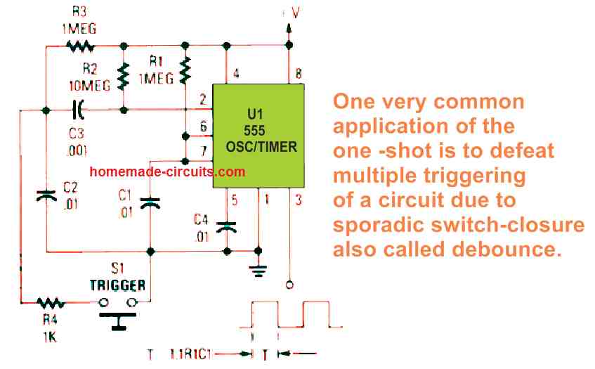 In the one-shot monostable circuit as demonstrated in the figure above, the 555 timer is triggered using a pushbutton S1. Just before the activation of S1, capacitor C1 is charged to the positive supply rail level through R1.
Next, the moment S1 is pressed, it causes C1 to discharge very fast by means of R4, which generates an instantaneous sharp negative surge voltage.
Any intermittent spikes happening due to the switch debounce on pressing S1, can be effectively eliminated due to the presence of R1 and C1, which enables a perfectly clean, negative-going spike.
This spike is subsequently allowed to move through C2 to pin 2 of 555 U1, triggering the monostable to activate, and generate a zero interference, clean square-wave output with a period of T= 1.1 x R1 x C1. Then, as soon as the S1 is released, causes C1 to recharge to the +V potential level so that the circuit now goes in the standby mode, ready for the the next clean push button actuation cycle.
The monostable design allows a single fixed high output pulse when the S1 button is pressed, regardless of how long S1 is held depressed.
However the monostable circuit will be able to retrigger, as fast as S1 may allow to be reactuated.
But it has to be ensured that the lowest possible output pulse duration of the design must be longer than the typical debounce period of the switch itself, mostly this should be around 10 ms or less.
In the one-shot monostable circuit as demonstrated in the figure above, the 555 timer is triggered using a pushbutton S1. Just before the activation of S1, capacitor C1 is charged to the positive supply rail level through R1.
Next, the moment S1 is pressed, it causes C1 to discharge very fast by means of R4, which generates an instantaneous sharp negative surge voltage.
Any intermittent spikes happening due to the switch debounce on pressing S1, can be effectively eliminated due to the presence of R1 and C1, which enables a perfectly clean, negative-going spike.
This spike is subsequently allowed to move through C2 to pin 2 of 555 U1, triggering the monostable to activate, and generate a zero interference, clean square-wave output with a period of T= 1.1 x R1 x C1. Then, as soon as the S1 is released, causes C1 to recharge to the +V potential level so that the circuit now goes in the standby mode, ready for the the next clean push button actuation cycle.
The monostable design allows a single fixed high output pulse when the S1 button is pressed, regardless of how long S1 is held depressed.
However the monostable circuit will be able to retrigger, as fast as S1 may allow to be reactuated.
But it has to be ensured that the lowest possible output pulse duration of the design must be longer than the typical debounce period of the switch itself, mostly this should be around 10 ms or less.
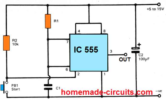 Push button PB1 has to be quickly released before the output pulse turns OFF, so that a correct working of the circuit is implemented.
This may not be the situation in case an output pulse of just a milliseconds is wanted, and most likely in this situation the pulse period is going to be equal to the of PB1 pressing time period, and not the intended time period that is set by the timing components R1 and C1.
Push button PB1 has to be quickly released before the output pulse turns OFF, so that a correct working of the circuit is implemented.
This may not be the situation in case an output pulse of just a milliseconds is wanted, and most likely in this situation the pulse period is going to be equal to the of PB1 pressing time period, and not the intended time period that is set by the timing components R1 and C1.
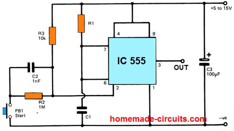 This provides the required short trigger pulse, and regardless of the time PB1 remains depressed, it is actually the R3 and C2 time constants that determines the final length of the output switch ON trigger pulse.
During the procedure, R2 discharges capacitor C2 quickly as soon as PB1 pressing is removed, which enables the circuit to be almost immediately prepared for the next PB1 pressed monostable operation.
One small difficulty that you may find with this enhanced push button monostable circuit is the multiple triggering of the circuit, which may be caused due to IC1 getting triggered during the periods PB1 push is released.
This may happen due to the mechanical contact bounce effect in the switch PB1.
This provides the required short trigger pulse, and regardless of the time PB1 remains depressed, it is actually the R3 and C2 time constants that determines the final length of the output switch ON trigger pulse.
During the procedure, R2 discharges capacitor C2 quickly as soon as PB1 pressing is removed, which enables the circuit to be almost immediately prepared for the next PB1 pressed monostable operation.
One small difficulty that you may find with this enhanced push button monostable circuit is the multiple triggering of the circuit, which may be caused due to IC1 getting triggered during the periods PB1 push is released.
This may happen due to the mechanical contact bounce effect in the switch PB1.
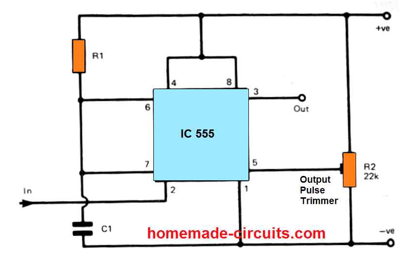 On the contrary if we reduce the pin#5 voltage, also causes a decrease in this threshold voltage which results in the shortening of the output pulse duration.
This shown IC 555 monostable circuit provides an extremely large trimming range of approximately from -85% to +400%.
On the contrary if we reduce the pin#5 voltage, also causes a decrease in this threshold voltage which results in the shortening of the output pulse duration.
This shown IC 555 monostable circuit provides an extremely large trimming range of approximately from -85% to +400%.
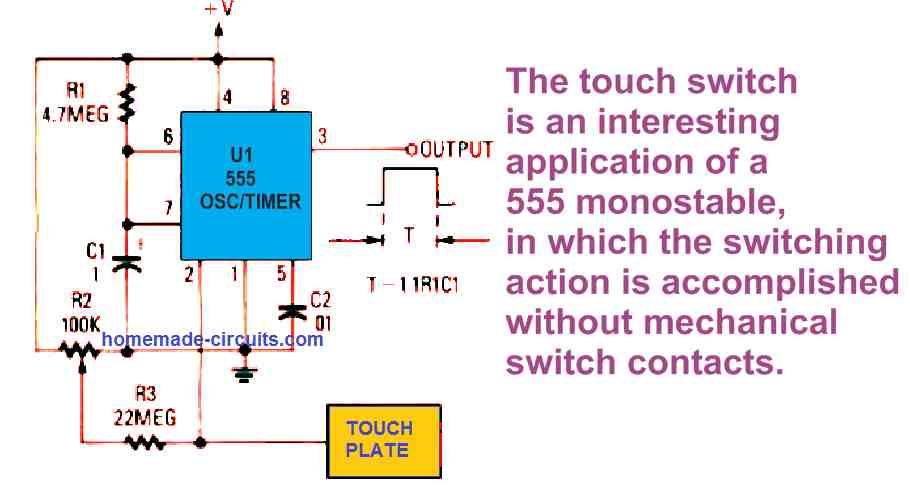 In this design, the switching function is achieved without involving any kind of traditional mechanized switch buttons.
The circuit is essentially an old-fashioned 555 monostable, having just one key distinction, which is its style of triggering.
The resistor R1 is used for biasing the trigger input which helps to improve the sensitivity of the monostable circuit.
In this type of circuit, the trigger input requires very small amount of current during the time it remains above its 1/3 of the positive threshold.
While using threshold control, resistor R2, is set to ensure the voltage at pin 2 is kept above 1/3 +V the monostable circuit output is held low until triggered.
As soon as the touch plate is contacted, the capacitance of the body (that now becomes effectively parallel with R3) causes the actual impedance between pin 2 and ground to drop.
Due to this pin 2 potential is pulled below the 1/3 +V threshold.
This results in the triggering of the IC U1, causing an output pulse to genearte which has an ON time of T= 1.1 x R1 x C1.
It must be ensured that the set time period is longer than the average touch time on the touch plate.
If this rule is not followed will result in the the timer getting retriggered even before the first timing pulse cycle is actually completed.
As indicated in the Fig.
5, the timing period of the monostable is approximately 5 seconds.
The touch plate could be any metal plate organized for easy finger touching.
It may be also recommended to have some sort of feedback arranged such as an LED or buzzer, that will indicate the user regarding the successful touching and triggering of the circuit.
In this design, the switching function is achieved without involving any kind of traditional mechanized switch buttons.
The circuit is essentially an old-fashioned 555 monostable, having just one key distinction, which is its style of triggering.
The resistor R1 is used for biasing the trigger input which helps to improve the sensitivity of the monostable circuit.
In this type of circuit, the trigger input requires very small amount of current during the time it remains above its 1/3 of the positive threshold.
While using threshold control, resistor R2, is set to ensure the voltage at pin 2 is kept above 1/3 +V the monostable circuit output is held low until triggered.
As soon as the touch plate is contacted, the capacitance of the body (that now becomes effectively parallel with R3) causes the actual impedance between pin 2 and ground to drop.
Due to this pin 2 potential is pulled below the 1/3 +V threshold.
This results in the triggering of the IC U1, causing an output pulse to genearte which has an ON time of T= 1.1 x R1 x C1.
It must be ensured that the set time period is longer than the average touch time on the touch plate.
If this rule is not followed will result in the the timer getting retriggered even before the first timing pulse cycle is actually completed.
As indicated in the Fig.
5, the timing period of the monostable is approximately 5 seconds.
The touch plate could be any metal plate organized for easy finger touching.
It may be also recommended to have some sort of feedback arranged such as an LED or buzzer, that will indicate the user regarding the successful touching and triggering of the circuit.
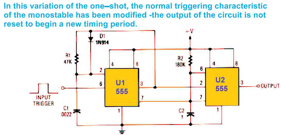 The circuit is different from the previous monostables since it works with a couple of IC 555's instead of one, Additionally, we do not have to reset the circuit to initiate a fresh timing cycle.
In this concept we can see the 555 timer U2 is wired like the normal monostable, and is triggered by a negative or ground pulse, supplied by 555 U1, which is hooked-up in the form of a basic inverting monostable.
The 555 U1's discharge pin 7 is wired to hold C2 for the time-span determined by the U1's output pulse period.
In the normal working conditions, when the trigger pulses tend to be longer than the time period U2, the output pulses appear with the rate of the input cycles, and the width of the output pulses corresponds to 1.1xR2xC2.
When the trigger pulses have shorter time duration than 1.1 x R2 x C2, the voltage across C2 is forced to come back to zero along with each pulse.
As a result, C2 is never able to attain the 2/3 + V threshold as determined by the components R1/C2 for U2; which consequently causes U2 to never time out.
With the above conditions, the output of the circuit continues to be at a constant high DC level, and carries on in this way for so long as the input triggers are obtained with a time period lower than 1.1 x R2 x C2.
The Fig.
6 concept could be modified to work with just about any rate that corresponds with the appropriate selection of component values for 555.
The IC U1 555's output pulse-width of must be maintained at a certain modest percentage to that of IC 555 U2, ensuring that the pulse-width are sufficiently long and are able to satisfy the full discharge of C2 during the 555 U1's timing period.
The circuit is different from the previous monostables since it works with a couple of IC 555's instead of one, Additionally, we do not have to reset the circuit to initiate a fresh timing cycle.
In this concept we can see the 555 timer U2 is wired like the normal monostable, and is triggered by a negative or ground pulse, supplied by 555 U1, which is hooked-up in the form of a basic inverting monostable.
The 555 U1's discharge pin 7 is wired to hold C2 for the time-span determined by the U1's output pulse period.
In the normal working conditions, when the trigger pulses tend to be longer than the time period U2, the output pulses appear with the rate of the input cycles, and the width of the output pulses corresponds to 1.1xR2xC2.
When the trigger pulses have shorter time duration than 1.1 x R2 x C2, the voltage across C2 is forced to come back to zero along with each pulse.
As a result, C2 is never able to attain the 2/3 + V threshold as determined by the components R1/C2 for U2; which consequently causes U2 to never time out.
With the above conditions, the output of the circuit continues to be at a constant high DC level, and carries on in this way for so long as the input triggers are obtained with a time period lower than 1.1 x R2 x C2.
The Fig.
6 concept could be modified to work with just about any rate that corresponds with the appropriate selection of component values for 555.
The IC U1 555's output pulse-width of must be maintained at a certain modest percentage to that of IC 555 U2, ensuring that the pulse-width are sufficiently long and are able to satisfy the full discharge of C2 during the 555 U1's timing period.
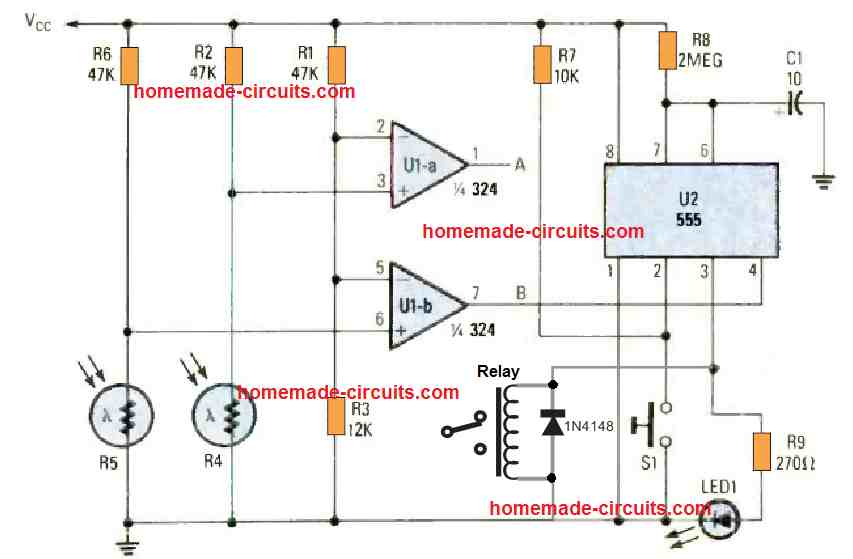 At this point, with the values the ersistors R1 and R3 have, less than 50 percent of the supply voltage, which is around 1.02 volt, reaches the inverting input of U1b.
With the op amp inverting input of U1b having a increased voltage difference than the non-inverting input, the U1 op amp output becomes low.
This low output reaches the pin 4 (reset) of U2, disabling the IC 555 function, which mens the implemtation of a negative or ground trigger pulse fails to reach the at pin 2 which keeps the initialization of the monostable switching cycle disabled.
But as the sun goes down, the R5 resistance goes higher and touches the maximum value of approximately 0.5 megohm.
Due to this increase in the R5 resistance, the voltage drop across it as well raises, causing the U1b output to get less negative.
As soon as the R5 resistance goes over the 47k limit, the U1b output instantly turns positive, eliminating the disabling signal utilized to pin 4 of IC 555 U2.
Pushing S1 in this situation can trigger ON the IC 555 monostable timing cycle, causing pin 3 of U2 to go high, and switch ON any device connected to pin3 of the monostable IC 555. For example a relay could be connected across pin3 and ground, and the N/O contacts of the relay wired across a series lamp and AC mains supply, which would cause the lamp to light up in this scenario, and remain illuminated as long as the monostable cycle keeps the relay ON.
At this point, with the values the ersistors R1 and R3 have, less than 50 percent of the supply voltage, which is around 1.02 volt, reaches the inverting input of U1b.
With the op amp inverting input of U1b having a increased voltage difference than the non-inverting input, the U1 op amp output becomes low.
This low output reaches the pin 4 (reset) of U2, disabling the IC 555 function, which mens the implemtation of a negative or ground trigger pulse fails to reach the at pin 2 which keeps the initialization of the monostable switching cycle disabled.
But as the sun goes down, the R5 resistance goes higher and touches the maximum value of approximately 0.5 megohm.
Due to this increase in the R5 resistance, the voltage drop across it as well raises, causing the U1b output to get less negative.
As soon as the R5 resistance goes over the 47k limit, the U1b output instantly turns positive, eliminating the disabling signal utilized to pin 4 of IC 555 U2.
Pushing S1 in this situation can trigger ON the IC 555 monostable timing cycle, causing pin 3 of U2 to go high, and switch ON any device connected to pin3 of the monostable IC 555. For example a relay could be connected across pin3 and ground, and the N/O contacts of the relay wired across a series lamp and AC mains supply, which would cause the lamp to light up in this scenario, and remain illuminated as long as the monostable cycle keeps the relay ON.
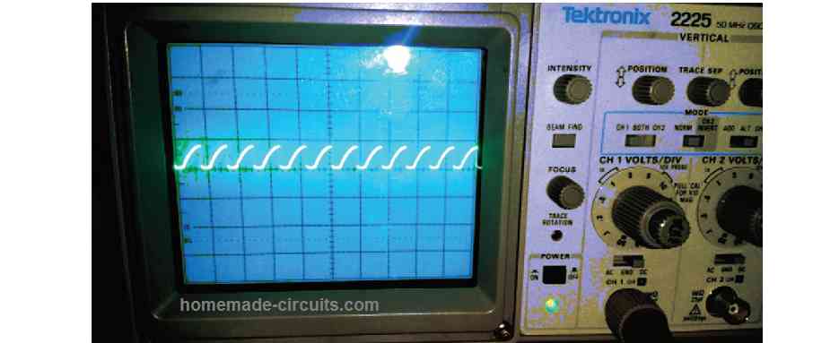 The waveform is named sawtooth, since its appearance resembles the teeth of a sawtooth cutter device.
The above explained sawtooth waveform could be given an opposite shape by generating the waveform in an opposite manner.
Here, the waveform voltage first increases suddenly or instantly to the peak value, then falls slowly in a slanting shape until it reaches the zero mark, and then again rises suddenly to the peak value, and this keeps repeating.
When a sawtooth waveform is triggered intermittently, or momentarily or in a one-shot manner, then it is called a ramp waveform.
In the following article we will discuss simple circuits using IC 555 to generate sawtooth waveform as well as ramp waveform.
The waveform is named sawtooth, since its appearance resembles the teeth of a sawtooth cutter device.
The above explained sawtooth waveform could be given an opposite shape by generating the waveform in an opposite manner.
Here, the waveform voltage first increases suddenly or instantly to the peak value, then falls slowly in a slanting shape until it reaches the zero mark, and then again rises suddenly to the peak value, and this keeps repeating.
When a sawtooth waveform is triggered intermittently, or momentarily or in a one-shot manner, then it is called a ramp waveform.
In the following article we will discuss simple circuits using IC 555 to generate sawtooth waveform as well as ramp waveform.
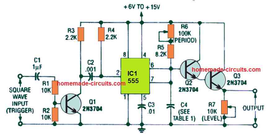 The circuit is actually a customized monostable multivibrator which is activated through an external square wave TRIGGER at pin 2, which is acquired via capacitor C2 through the collector of Q1 transistor.
Notice that IC 555 pin 3 which is commonly used as the output in most IC 555 based circuits is actually empty and unconnected here.
The voltage around C4 (which works like the timing component) is generally zero, however the moment the IC 555 is triggered, C4 begins charging exponentially via resistor R5 and TIME PERIOD potentiometer R6 to a level of 2/3rd of the supply voltage.
During this period, the monostable period comes to an end and the voltage across C4 declines suddenly to zero.
The circuit is actually a customized monostable multivibrator which is activated through an external square wave TRIGGER at pin 2, which is acquired via capacitor C2 through the collector of Q1 transistor.
Notice that IC 555 pin 3 which is commonly used as the output in most IC 555 based circuits is actually empty and unconnected here.
The voltage around C4 (which works like the timing component) is generally zero, however the moment the IC 555 is triggered, C4 begins charging exponentially via resistor R5 and TIME PERIOD potentiometer R6 to a level of 2/3rd of the supply voltage.
During this period, the monostable period comes to an end and the voltage across C4 declines suddenly to zero.
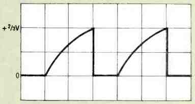 Waveform across C4
This gives rise to the output sawtooth waveform as shown above, across capacitor C4 by means of Q2, Q3 buffer transistors, and LEVEL control potentiometer R7.
The sawtooth waveform period or pulse width could be adjusted right from 9 microseconds to 1.2 seconds using the capacitors for C4 as detailed in Table 1.
The circuit's highest functional repetition frequency is around 100 kHz.
The sawtooth generator should be activated or triggered with input waveforms having rectangular shape and with quick rise and fall periods.
Potentiometer R6 is used for controlling the sawtooth time period through a resistor decade, and potentiometer R7 is wired to controls the amplitude of the output waveform.
Waveform across C4
This gives rise to the output sawtooth waveform as shown above, across capacitor C4 by means of Q2, Q3 buffer transistors, and LEVEL control potentiometer R7.
The sawtooth waveform period or pulse width could be adjusted right from 9 microseconds to 1.2 seconds using the capacitors for C4 as detailed in Table 1.
The circuit's highest functional repetition frequency is around 100 kHz.
The sawtooth generator should be activated or triggered with input waveforms having rectangular shape and with quick rise and fall periods.
Potentiometer R6 is used for controlling the sawtooth time period through a resistor decade, and potentiometer R7 is wired to controls the amplitude of the output waveform.
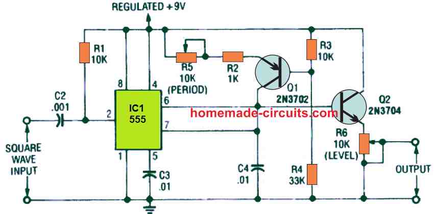 The output linear sawtooth waveform or the ramp waveform as shown below is obtained from the slider arm of the LEVEL potentiometer R6, that is connected across the capacitor C4 via Q2.
Observe that the rounded ramps in the earlier waveform happen to be flattened or compressed in the below shown linear sawtooth waveform.
The output linear sawtooth waveform or the ramp waveform as shown below is obtained from the slider arm of the LEVEL potentiometer R6, that is connected across the capacitor C4 via Q2.
Observe that the rounded ramps in the earlier waveform happen to be flattened or compressed in the below shown linear sawtooth waveform.
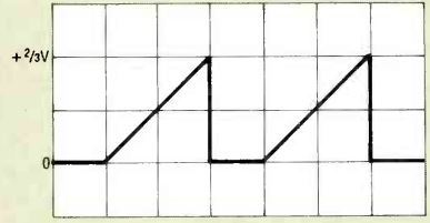 As soon as a capacitor C4 is charged through a constant current source, the voltage across it goes up with a consistent linear rate which can be depicted with the equation:
Volts/second = amperes/farad
Through the introduction of further simple values, alternate equations for the rate of voltage rise can be given as:
V/��s = A/��F, or V/ms = mA/��F
The above equations suggest that the rate of voltage rise could be higher either by increasing charging current for the C4 or by decreasing the C4 value.
The charging current in the second sawtooth generator circuit above could be changed, by a measure from 90 microamperes to 1 milliampere using the PERIOD potentiometer R5. This would result in a 0.01 microfarad timing capacitor producing a rates-of-rise of 9 volts per millisecond to 100 volts per millisecond.
Every one-shot or monostable cycle of the 555 comes to an end as soon as the voltage across C4 attains 2/3rd of the supply voltage.
As displayed in the second linear sawtooth generator circuit, the input supply is 9 volts, which means 2/3rd of 9 volts will be 6 volts, and the the ramp voltage amplitude waveforms will be as shown above.
The sawtooth waveform of the circuit include periods that can be varied from 666 microseconds (2/3 millisecond) to 60 microseconds (6/100 millisecond).
It is possible to increase this intervals beyond the above values by increasing the value of C4, or the values could be lowered by lowering the C4 value.
In the proposed sawtooth generator circuit, stable timing intervals is strictly dependent on a stable voltage source.
As soon as a capacitor C4 is charged through a constant current source, the voltage across it goes up with a consistent linear rate which can be depicted with the equation:
Volts/second = amperes/farad
Through the introduction of further simple values, alternate equations for the rate of voltage rise can be given as:
V/��s = A/��F, or V/ms = mA/��F
The above equations suggest that the rate of voltage rise could be higher either by increasing charging current for the C4 or by decreasing the C4 value.
The charging current in the second sawtooth generator circuit above could be changed, by a measure from 90 microamperes to 1 milliampere using the PERIOD potentiometer R5. This would result in a 0.01 microfarad timing capacitor producing a rates-of-rise of 9 volts per millisecond to 100 volts per millisecond.
Every one-shot or monostable cycle of the 555 comes to an end as soon as the voltage across C4 attains 2/3rd of the supply voltage.
As displayed in the second linear sawtooth generator circuit, the input supply is 9 volts, which means 2/3rd of 9 volts will be 6 volts, and the the ramp voltage amplitude waveforms will be as shown above.
The sawtooth waveform of the circuit include periods that can be varied from 666 microseconds (2/3 millisecond) to 60 microseconds (6/100 millisecond).
It is possible to increase this intervals beyond the above values by increasing the value of C4, or the values could be lowered by lowering the C4 value.
In the proposed sawtooth generator circuit, stable timing intervals is strictly dependent on a stable voltage source.
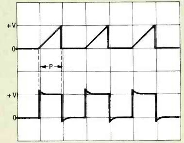 It could be activated through external square waves, by using an appropriate trigger selector circuit.
The upper ramp output waveform is connected to the X axis of an oscilloscope using a good amplifier stage.
The timebase circuit as shown in the above figure can coordinate signals with trigger frequencies upto 150 KHz.
At increased frequencies, the input signals should be broken down by a single-or multi-decade frequency divider.
With this strategy, the timebase could be implemented to view input signals at megahertz frequencies
It could be activated through external square waves, by using an appropriate trigger selector circuit.
The upper ramp output waveform is connected to the X axis of an oscilloscope using a good amplifier stage.
The timebase circuit as shown in the above figure can coordinate signals with trigger frequencies upto 150 KHz.
At increased frequencies, the input signals should be broken down by a single-or multi-decade frequency divider.
With this strategy, the timebase could be implemented to view input signals at megahertz frequencies
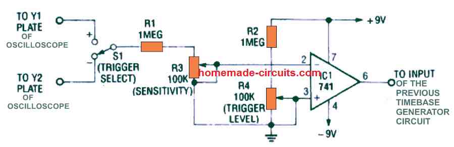 Op amp IC1 (a ��A741) provides a reference voltage applied to its non-inverting input pin 3 through TRIGGER LEVEL potentiometer R4. The signal voltage is subsequently fed to IC1's inverting pin 2 via switch S1, resistor R1 and SENSITIVY potentiometer R3.
Switch S1 chooses either in-phase or out-of-phase input signals from the Y-channel amplifier driver for the oscilloscope, enabling the range of either the plus or minus trigger modes.
The output from the IC 741 is connected straight to the C1 input of the earlier time base generator circuit.
Op amp IC1 (a ��A741) provides a reference voltage applied to its non-inverting input pin 3 through TRIGGER LEVEL potentiometer R4. The signal voltage is subsequently fed to IC1's inverting pin 2 via switch S1, resistor R1 and SENSITIVY potentiometer R3.
Switch S1 chooses either in-phase or out-of-phase input signals from the Y-channel amplifier driver for the oscilloscope, enabling the range of either the plus or minus trigger modes.
The output from the IC 741 is connected straight to the C1 input of the earlier time base generator circuit.
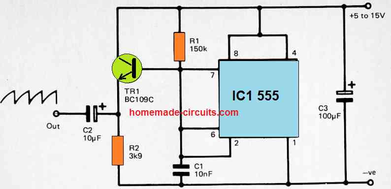 The sawtooth waveform is actually extracted across the capacitor C1, while the short negative pulses available at pin 3 of the IC1 is not used.
Tr1 and R1 are configured like a simple emitter follower buffer stage in order to achieve a fairly low output impedance via the high impedance signal across C1.
The indicated values offer an running frequency of approximately 1kHz (960Hz through calculations).
That said, the R1, and C1 values might certainly be altered to provide a new output frequency.
It is recommended to avoid making R1 too much bigger than the chosen value of 150k, otherwise loading on the timing circuitry might stop the sawtooth waveform generation from performing correctly.
The sawtooth waveform is actually extracted across the capacitor C1, while the short negative pulses available at pin 3 of the IC1 is not used.
Tr1 and R1 are configured like a simple emitter follower buffer stage in order to achieve a fairly low output impedance via the high impedance signal across C1.
The indicated values offer an running frequency of approximately 1kHz (960Hz through calculations).
That said, the R1, and C1 values might certainly be altered to provide a new output frequency.
It is recommended to avoid making R1 too much bigger than the chosen value of 150k, otherwise loading on the timing circuitry might stop the sawtooth waveform generation from performing correctly.
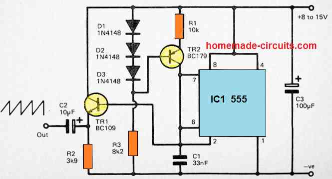 The circuit functions at approximately 1kHz using the selected values for R1 and C1. However, it is possible to adjust the output frequency by varying the values of either R1 or C1. R1 must be selected between Ik and 47k range for getting optimal response from the circuit.
 When this happens pin 7 again turns high initiating the charging action on the capacitor until it teaches the 2/3rd supply level.
The cycle continues infinitely establishing the astable mode of the circuit.
The above working of the astable results in two types of oscillations to occur across C1 and across the output pin 3 of the IC.
Across C1, the exponential rise and fall of voltage creates a sawtooth frequency to appear.
The internal flip flop responds to these sawtooth frequency and converts then into rectangular waves at the output pin 3 of the IC.
This provides us with the required rectangular wave oscillations at the output of the IC pin 3.
Since the oscillation frequency entirely depends on R1, R2, and C1, the user is able to alter the values of these components to get any desired values for the ON OFF periods of the oscillation frequencies, which is also called PWM control or duty cycle control.
When this happens pin 7 again turns high initiating the charging action on the capacitor until it teaches the 2/3rd supply level.
The cycle continues infinitely establishing the astable mode of the circuit.
The above working of the astable results in two types of oscillations to occur across C1 and across the output pin 3 of the IC.
Across C1, the exponential rise and fall of voltage creates a sawtooth frequency to appear.
The internal flip flop responds to these sawtooth frequency and converts then into rectangular waves at the output pin 3 of the IC.
This provides us with the required rectangular wave oscillations at the output of the IC pin 3.
Since the oscillation frequency entirely depends on R1, R2, and C1, the user is able to alter the values of these components to get any desired values for the ON OFF periods of the oscillation frequencies, which is also called PWM control or duty cycle control.
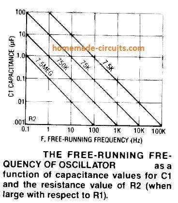 The graph above provides us with the relationship between R1, and C1.
R2 is ignored here because its value is negligibly small compared to R2.
The graph above provides us with the relationship between R1, and C1.
R2 is ignored here because its value is negligibly small compared to R2.
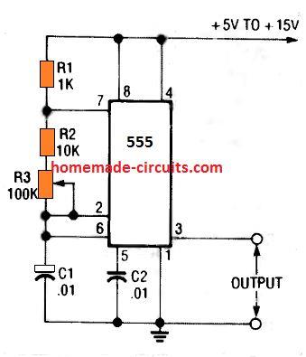 In the above set up, the frequency of oscillation can be varied right from 650 Hz, to 7.2 kHz through the indicated pot variations.
This range can be even further increased and enhanced by adding a switch for selecting different values for C1, since C1 is also directly responsible for setting the output frequency.
In the above set up, the frequency of oscillation can be varied right from 650 Hz, to 7.2 kHz through the indicated pot variations.
This range can be even further increased and enhanced by adding a switch for selecting different values for C1, since C1 is also directly responsible for setting the output frequency.
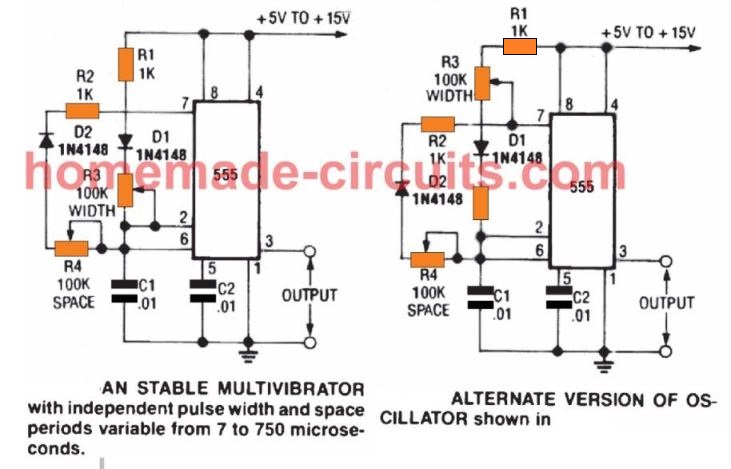 The figure above shows how a variable mark space ratio facility can be added to any basic IC 555 astable oscillator circuit through a couple diodes and a potentiometer.
The feature allows the user to get any desired PWM or adjustable ON OFF periods for the oscillations at the output pin 3 of the IC.
In the left side diagram, the network involving R1, D1, and the pot R3 alternately charges C1, while the pot R4, D2 and R2 alternately discharges the C1 capacitor.
R2, and R4 determine the rate of charge/discharge of C1, and can be adjusted suitably for getting the desired ON/OFF ratio for the output frequency.
The right side diagram shows R3 position shifted in series with R1. In this configuration, the charge time of C1 is fixed by D1 and its series resistor, while the pot only allows the control for the discharge time of C1, hence the OFF time of output pulses.
The other pot R3 essentially helps to alter the frequency of the output instead of the PWM.
The figure above shows how a variable mark space ratio facility can be added to any basic IC 555 astable oscillator circuit through a couple diodes and a potentiometer.
The feature allows the user to get any desired PWM or adjustable ON OFF periods for the oscillations at the output pin 3 of the IC.
In the left side diagram, the network involving R1, D1, and the pot R3 alternately charges C1, while the pot R4, D2 and R2 alternately discharges the C1 capacitor.
R2, and R4 determine the rate of charge/discharge of C1, and can be adjusted suitably for getting the desired ON/OFF ratio for the output frequency.
The right side diagram shows R3 position shifted in series with R1. In this configuration, the charge time of C1 is fixed by D1 and its series resistor, while the pot only allows the control for the discharge time of C1, hence the OFF time of output pulses.
The other pot R3 essentially helps to alter the frequency of the output instead of the PWM.
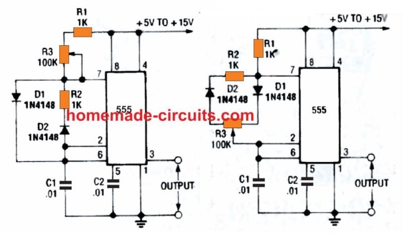 Alternatively, as shown in the above figures, it may be also possible to connect the IC 555 in the astable mode for discretely adjusting the mark/space (ON time/OFF time) ratio without affecting the oscillatory frequency.
In these configurations the length of the pulses inherently increases as the interval of space is reduced, and vice versa.
Due to this, the total period of each square wave cycle remains constant.
The main feature of these circuits is the variable duty cycle, which can be varied right from 1% to 99% with the help of the given potentiometer R3.
In the left side figure, C1 is charged alternately by R1, the upper half of R3, and D1, while it's discharged by means of D2, R2, and the lower half of potentiometer R3. In the right side figure, C1 is alternately charged via R1 and D1 and the right half of potentiometer R3, and it discharged through the left half potentiometer R3, D2, and R2.
In both the above astables the value of C1 sets the oscillatory frequency to around 1.2 kHz.
Alternatively, as shown in the above figures, it may be also possible to connect the IC 555 in the astable mode for discretely adjusting the mark/space (ON time/OFF time) ratio without affecting the oscillatory frequency.
In these configurations the length of the pulses inherently increases as the interval of space is reduced, and vice versa.
Due to this, the total period of each square wave cycle remains constant.
The main feature of these circuits is the variable duty cycle, which can be varied right from 1% to 99% with the help of the given potentiometer R3.
In the left side figure, C1 is charged alternately by R1, the upper half of R3, and D1, while it's discharged by means of D2, R2, and the lower half of potentiometer R3. In the right side figure, C1 is alternately charged via R1 and D1 and the right half of potentiometer R3, and it discharged through the left half potentiometer R3, D2, and R2.
In both the above astables the value of C1 sets the oscillatory frequency to around 1.2 kHz.
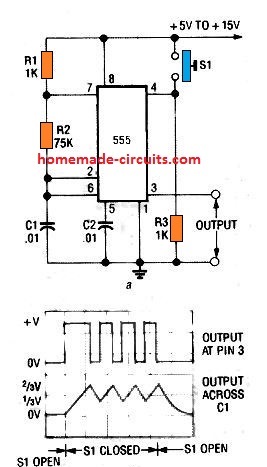 You can trigger an IC 555 astable oscillator ON/OFF in a few simple ways.
It can be done using push buttons or through an electronic input signal.
In the figure above pin 4 which is the reset pin of the IC is grounded through R3, and a push-to-ON switch is connected across the positive supply line.
Pin 4 of IC 555 needs minimum 0.7 V to remain biased and to keep the IC functioning enabled.
Pressing the button enables the IC astable oscillator function, while releasing the switch removes the biasing from pin 4 and the IC function gets disabled.
This can be also implemented through a external positive signal on pin 4 with the switch removed and R3 connected as is.
You can trigger an IC 555 astable oscillator ON/OFF in a few simple ways.
It can be done using push buttons or through an electronic input signal.
In the figure above pin 4 which is the reset pin of the IC is grounded through R3, and a push-to-ON switch is connected across the positive supply line.
Pin 4 of IC 555 needs minimum 0.7 V to remain biased and to keep the IC functioning enabled.
Pressing the button enables the IC astable oscillator function, while releasing the switch removes the biasing from pin 4 and the IC function gets disabled.
This can be also implemented through a external positive signal on pin 4 with the switch removed and R3 connected as is.
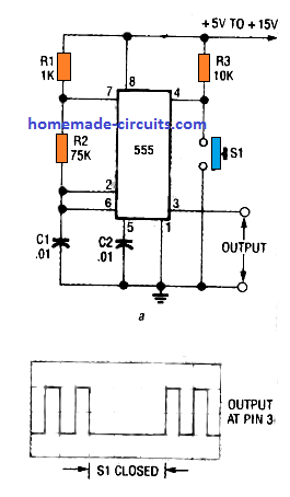 In the other alternative as shown above, pin 4 of the IC can be seen permanently biased via R3 and the positive supply.
Here the push button is connected across pin 4 and ground.
This implies when the push button is pressed disables the IC output square waves, causing the output to turn 0V.
Releasing the push button commences the generation of the astable square waves normally across pin 3 of the IC.
The same can be achieved through an externally applied negative signal or a 0 V signal at pin 4 with R3 connected as is.
In the other alternative as shown above, pin 4 of the IC can be seen permanently biased via R3 and the positive supply.
Here the push button is connected across pin 4 and ground.
This implies when the push button is pressed disables the IC output square waves, causing the output to turn 0V.
Releasing the push button commences the generation of the astable square waves normally across pin 3 of the IC.
The same can be achieved through an externally applied negative signal or a 0 V signal at pin 4 with R3 connected as is.
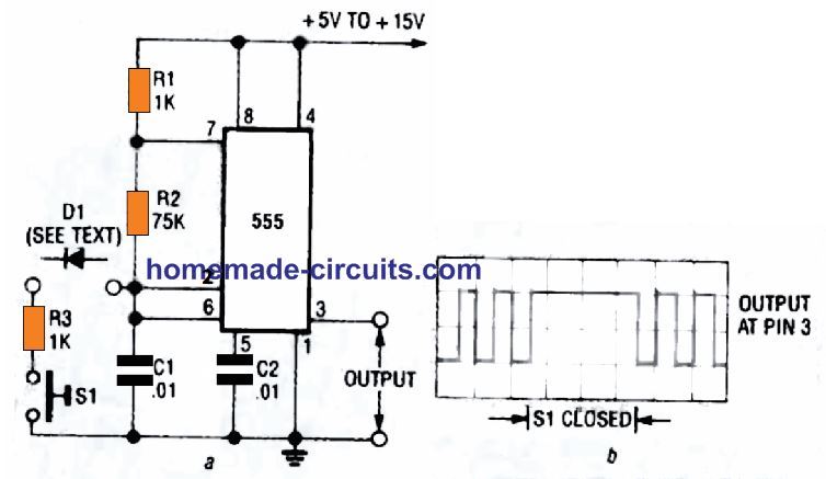 In our earlier discussions we learned how the pulse generation of a IC 555 could be controlled through pin 4.
Now we will see how the same may be achieved through pin 2 of the IC as shown above.
When S1 is pressed, pin 2 is suddenly applied with a ground potential, causing the voltage across C1 to drop below 1/3rd Vcc.
As we know that when pin 2 voltage or the charge level across C1 is held below 1/3rd Vcc,, the output pin 3 goes high permanently.
Therefore pressing S1 causes a voltage drop across C1 below 1/3rd Vcc forcing the output pin 3 to go high as long as S1 remains pressed.
This inhibits the normal working of astable oscillations.
When the push button is released, the astbale function is restored back to normal conditions.
The waveform on the right side acknowledges the pin 3 response to the pressing of the push button.
The above operation can be likewise controlled using an external digital circuit through the diode D1. A negative logic at the cathode of the diode initiates the above actions, while a positive logic has no effect, and allows the functions of the astable to restore its normal working.
In our earlier discussions we learned how the pulse generation of a IC 555 could be controlled through pin 4.
Now we will see how the same may be achieved through pin 2 of the IC as shown above.
When S1 is pressed, pin 2 is suddenly applied with a ground potential, causing the voltage across C1 to drop below 1/3rd Vcc.
As we know that when pin 2 voltage or the charge level across C1 is held below 1/3rd Vcc,, the output pin 3 goes high permanently.
Therefore pressing S1 causes a voltage drop across C1 below 1/3rd Vcc forcing the output pin 3 to go high as long as S1 remains pressed.
This inhibits the normal working of astable oscillations.
When the push button is released, the astbale function is restored back to normal conditions.
The waveform on the right side acknowledges the pin 3 response to the pressing of the push button.
The above operation can be likewise controlled using an external digital circuit through the diode D1. A negative logic at the cathode of the diode initiates the above actions, while a positive logic has no effect, and allows the functions of the astable to restore its normal working.
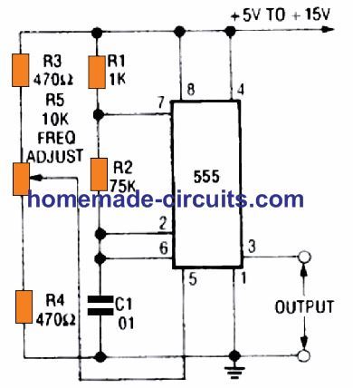 In the above figure adjusting the pot generates a varying potential at pin 5 which causes the output pulse width of the oscillation frequency to change accordingly.
Since the modulation causes the output pulse width to change it also affects the frequency, since C1 is forced to change its charge/discharge periods depending on the pot setting.
When a varying AC having an amplitude between 0V, and Vcc is applied at pin 5, the output PWM or pulse width also follows the varying AC amplitude generating a continuous train of widening and narrowing pulses a pin 3.
An AC signal can be also used for the modulation, simply by integrating pin 5 with an external AC though a 10uF capacitor.
To learn how to make Interesting alarm and Siren circuits using the above explained IC oscillator concept, you can read the whole article HERE
In the above figure adjusting the pot generates a varying potential at pin 5 which causes the output pulse width of the oscillation frequency to change accordingly.
Since the modulation causes the output pulse width to change it also affects the frequency, since C1 is forced to change its charge/discharge periods depending on the pot setting.
When a varying AC having an amplitude between 0V, and Vcc is applied at pin 5, the output PWM or pulse width also follows the varying AC amplitude generating a continuous train of widening and narrowing pulses a pin 3.
An AC signal can be also used for the modulation, simply by integrating pin 5 with an external AC though a 10uF capacitor.
To learn how to make Interesting alarm and Siren circuits using the above explained IC oscillator concept, you can read the whole article HERE
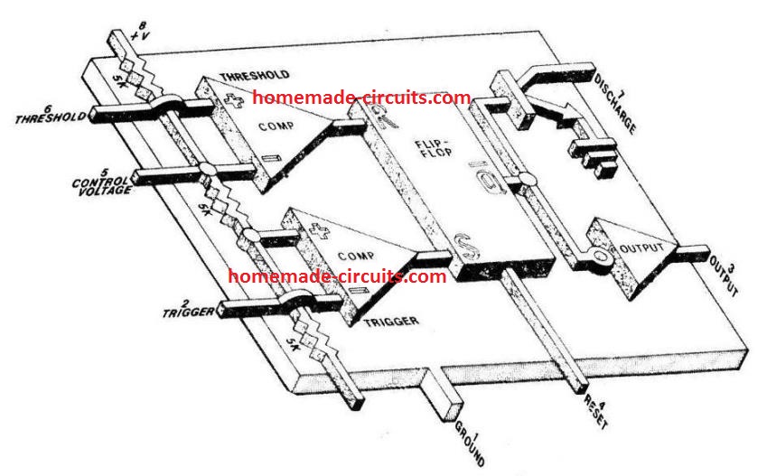 The stage involving the three 5 kohm resistors work like a voltage divider stage which produces 1/3rd voltage level at the non-inverting input of the trigger comparator op amp and a 2/3 voltage division on the inverting input of the threshold comparator op amp.
With these trigger inputs the two op amps control the R/S (reset/set) flip flop stage, which further control the ON/OFF conditions of the complementary output stage and the driver transistor Q6
The output state of the flip flop can be also set by triggering the reset pin 4 of the IC.
The stage involving the three 5 kohm resistors work like a voltage divider stage which produces 1/3rd voltage level at the non-inverting input of the trigger comparator op amp and a 2/3 voltage division on the inverting input of the threshold comparator op amp.
With these trigger inputs the two op amps control the R/S (reset/set) flip flop stage, which further control the ON/OFF conditions of the complementary output stage and the driver transistor Q6
The output state of the flip flop can be also set by triggering the reset pin 4 of the IC.
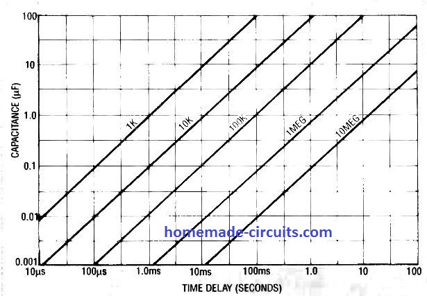 It shows a range of time delay curves and the linearly changing values with respect to the corresponding values of RT and C.
It is possible to set delays ranging from 10 ��seconds to 100 ��seconds by selecting appropriate values of capacitors from 0.001 ��F to 100 ��F and resistors from 1 k �� to 10 meg �� .
It shows a range of time delay curves and the linearly changing values with respect to the corresponding values of RT and C.
It is possible to set delays ranging from 10 ��seconds to 100 ��seconds by selecting appropriate values of capacitors from 0.001 ��F to 100 ��F and resistors from 1 k �� to 10 meg �� .
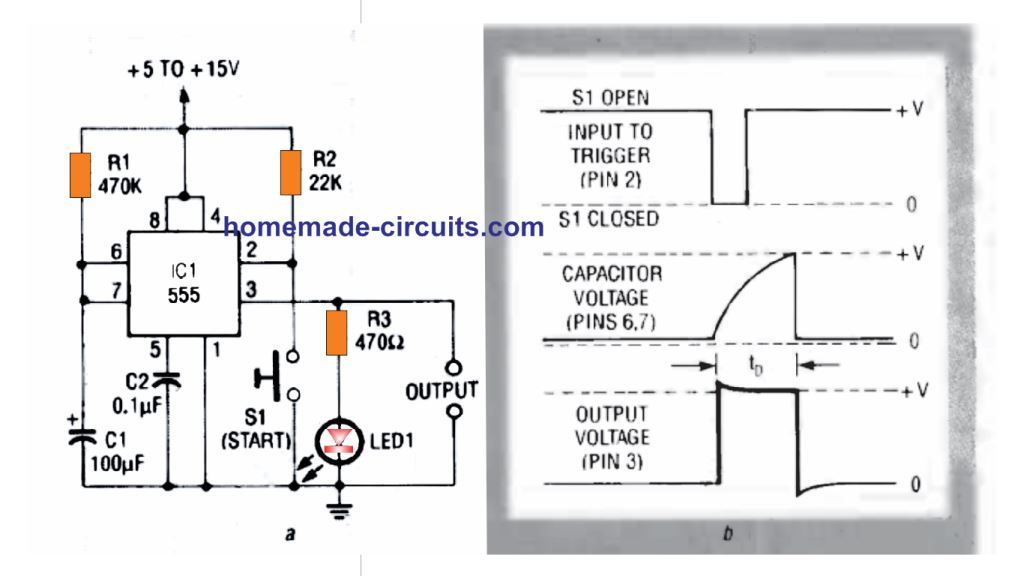 The adjoining figure shows the waveforms obtained across the indicated pinouts of the IC during the switching process.
The actions as described in the waveform image initiates as soon as the TRIGGER pin 2 is grounded with the pressing of momentary START Switch S1.
This instantly causes a rectangular pulse to appear at pin 3 and simultaneously generates an exponential sawtooth at DISCHARGE pin 7.
The time period for which this rectangular pulse remains active is determined by the values of R1, and C1. If R1 is replaced with a variable resistor, this output timing could be set as per user preference.
The LED illumination indicates the ON and OFF switching of the output pin 3 of the IC
The variable resistor can be in the form of a potentiometer as shown in the following figure 2.
The adjoining figure shows the waveforms obtained across the indicated pinouts of the IC during the switching process.
The actions as described in the waveform image initiates as soon as the TRIGGER pin 2 is grounded with the pressing of momentary START Switch S1.
This instantly causes a rectangular pulse to appear at pin 3 and simultaneously generates an exponential sawtooth at DISCHARGE pin 7.
The time period for which this rectangular pulse remains active is determined by the values of R1, and C1. If R1 is replaced with a variable resistor, this output timing could be set as per user preference.
The LED illumination indicates the ON and OFF switching of the output pin 3 of the IC
The variable resistor can be in the form of a potentiometer as shown in the following figure 2.
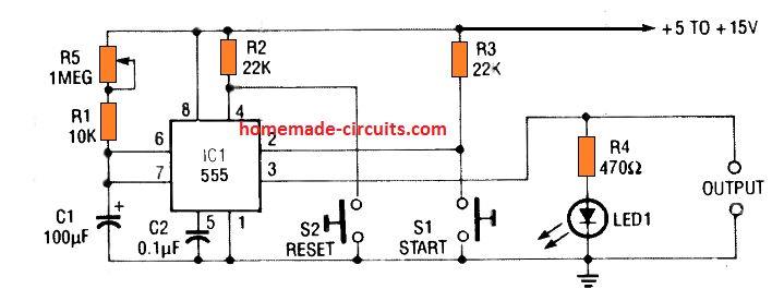 In this design the output can set to produce time periods from 1.1 seconds to 120 seconds through different adjustments of the pot R1.
Notice the series 10K resistor which is very important since it safeguards the IC from burning in case the pot is turned to its lowest value.
The 10 K series resistor also ensures the minimum resistance value required for the correct working of the circuit at the minimum pot setting.
Pressing the switch S1 momentarily enables the IC to start the timing sequence (pin 3 going high and LED turning ON), while pressing S2 reset button allows instant termination or resetting of the timing sequence so that the output pin 3 reverts to its original 0 V situation (LED turning OFF permanently)
The IC 555 allows the use of loads with maximum current specifications of up to 200 mA.
Although these loads are normally non-inductive types, an inductive load like a relay can be also effectively used directly across pin 3 and ground as shown in the following diagrams.
The 3rd figure below we can see that the relay can be wired across pin 3 and ground, and, pin 3 and positive.
Notice the freewheeling diode connected across the relay coil, it is highly recommended for neutralizing the dangerous back emfs from the relay coil during switch OFF instants.
In this design the output can set to produce time periods from 1.1 seconds to 120 seconds through different adjustments of the pot R1.
Notice the series 10K resistor which is very important since it safeguards the IC from burning in case the pot is turned to its lowest value.
The 10 K series resistor also ensures the minimum resistance value required for the correct working of the circuit at the minimum pot setting.
Pressing the switch S1 momentarily enables the IC to start the timing sequence (pin 3 going high and LED turning ON), while pressing S2 reset button allows instant termination or resetting of the timing sequence so that the output pin 3 reverts to its original 0 V situation (LED turning OFF permanently)
The IC 555 allows the use of loads with maximum current specifications of up to 200 mA.
Although these loads are normally non-inductive types, an inductive load like a relay can be also effectively used directly across pin 3 and ground as shown in the following diagrams.
The 3rd figure below we can see that the relay can be wired across pin 3 and ground, and, pin 3 and positive.
Notice the freewheeling diode connected across the relay coil, it is highly recommended for neutralizing the dangerous back emfs from the relay coil during switch OFF instants.
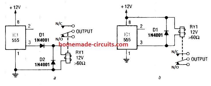 The relay contacts can be wired with an intended load for switching them ON/OFF in response to the set time intervals.
The 4rth circuit diagram shows the standard IC 555 adjustable timer circuit having two sets of timing ranges and an output relay for toggling the desired load.
The relay contacts can be wired with an intended load for switching them ON/OFF in response to the set time intervals.
The 4rth circuit diagram shows the standard IC 555 adjustable timer circuit having two sets of timing ranges and an output relay for toggling the desired load.
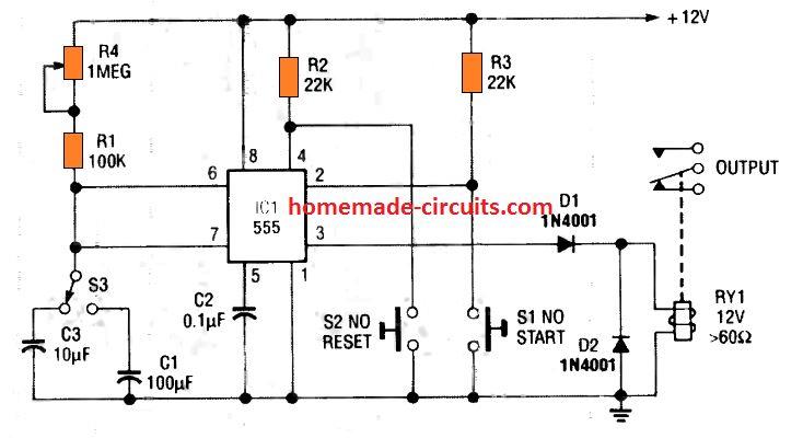 Although the schematic looks correct, this basic circuit may actually have a few negative aspects.
First, this design will drain some current continuously, even while the output of the circuit is in the off state.
Second, since the two capacitors C1, and C3 have a wide tolerance specs, the pot neds to be calibrated with two individual set up scales.
The above discussed flaws can be actually overcome, by configuring the circuit in the following manner.
Here we use a DPDT relay for the procedures.
Although the schematic looks correct, this basic circuit may actually have a few negative aspects.
First, this design will drain some current continuously, even while the output of the circuit is in the off state.
Second, since the two capacitors C1, and C3 have a wide tolerance specs, the pot neds to be calibrated with two individual set up scales.
The above discussed flaws can be actually overcome, by configuring the circuit in the following manner.
Here we use a DPDT relay for the procedures.
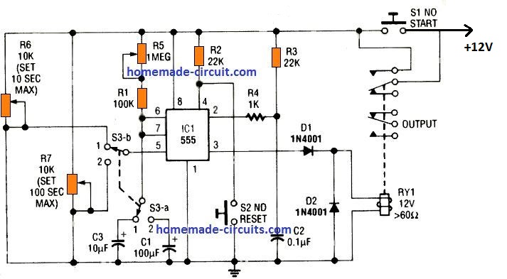 In this 5th IC 555 timer diagram we can see that the relay contacts are joined in parallel with the START switch S1, which are both in the "normally-open" mode, and ensures there's no current drain while the circuit is OFF.
To initiate the timing cycle, S1 is pressed momentarily.
This instantly powers the IC 555. At the onset, C2 can be expected to be fully discharged.
Due to this, a negative switch ON trigger is created at pin 2 of the IC, which initiates the timing cycle, and the relay RY1 switches ON.
The relay contacts which are connected in parallel with S1 enables the IC 555 to remain powered even after S2 is released.
When the set time period elapses, the relay is deactivated and its contacts revert to the N/C position disconnecting power from the entire circuit.
The timing delay output of the circuit is basically determined by R1 and potentiometer R5 values, along with the values of either C1 or C2, and depending on the position of the selector switch S3 a.
Having said this, we must also note that the timing is additionally affected by how the potentiometers R6 and R7 are adjusted.
They are switched through the switch S3 b and integrated with the CONTROL voltage pin 5 of the IC.
These potentiometers are introduced to effectively shunt the internal voltage of the IC 555, which might otherwise disturb the output timing of the system.
Due to this enhancement the circuit is now able to function with utmost accuracy even with capacitors having inconsistent tolerance levels.
Furthermore, the feature also allows the circuit to work with a solitary timing scale calibrated to read two individual timing ranges as per the positioning of the selector switch.
For setting up the above accurate IC 555 timer circuit, R5 must be initially adjusted to it maximum range.
After this, S3 may be selected to position 1.
Next, adjust R6 to get a 10 second ON timing output scale with some trial and error.
Follow the same procedures for the position 2 selection, through the pot R7 for getting an accurate scale of 100 seconds
In this 5th IC 555 timer diagram we can see that the relay contacts are joined in parallel with the START switch S1, which are both in the "normally-open" mode, and ensures there's no current drain while the circuit is OFF.
To initiate the timing cycle, S1 is pressed momentarily.
This instantly powers the IC 555. At the onset, C2 can be expected to be fully discharged.
Due to this, a negative switch ON trigger is created at pin 2 of the IC, which initiates the timing cycle, and the relay RY1 switches ON.
The relay contacts which are connected in parallel with S1 enables the IC 555 to remain powered even after S2 is released.
When the set time period elapses, the relay is deactivated and its contacts revert to the N/C position disconnecting power from the entire circuit.
The timing delay output of the circuit is basically determined by R1 and potentiometer R5 values, along with the values of either C1 or C2, and depending on the position of the selector switch S3 a.
Having said this, we must also note that the timing is additionally affected by how the potentiometers R6 and R7 are adjusted.
They are switched through the switch S3 b and integrated with the CONTROL voltage pin 5 of the IC.
These potentiometers are introduced to effectively shunt the internal voltage of the IC 555, which might otherwise disturb the output timing of the system.
Due to this enhancement the circuit is now able to function with utmost accuracy even with capacitors having inconsistent tolerance levels.
Furthermore, the feature also allows the circuit to work with a solitary timing scale calibrated to read two individual timing ranges as per the positioning of the selector switch.
For setting up the above accurate IC 555 timer circuit, R5 must be initially adjusted to it maximum range.
After this, S3 may be selected to position 1.
Next, adjust R6 to get a 10 second ON timing output scale with some trial and error.
Follow the same procedures for the position 2 selection, through the pot R7 for getting an accurate scale of 100 seconds
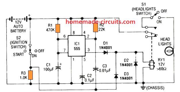 This 6th simple car headlight IC 555 based timer prevents the car headlights from shutting off as soon as the ignition is turned OFF.
Instead, the headlights are allowed to remain illuminated for some preset delay, once the driver locks the car ignition and walks off towards his destination which may be his home or office.
This allows the owner to see the path and enter the destination comfortably with visible illumination from the headlights.
Subsequently, when the delay period elapses the IC 555 circuit switches off the headlights.
This 6th simple car headlight IC 555 based timer prevents the car headlights from shutting off as soon as the ignition is turned OFF.
Instead, the headlights are allowed to remain illuminated for some preset delay, once the driver locks the car ignition and walks off towards his destination which may be his home or office.
This allows the owner to see the path and enter the destination comfortably with visible illumination from the headlights.
Subsequently, when the delay period elapses the IC 555 circuit switches off the headlights.
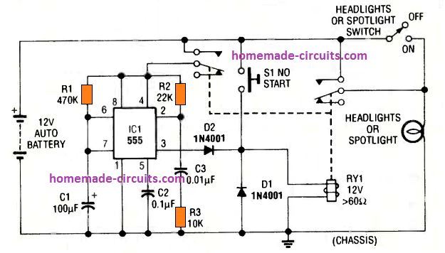 The circuit utilizes a DPDT relay having two sets of contacts.
The IC 555 monostable action is initiated by pressing S1 momentarily.
This energizes the relay, and both the contacts move upward and connect with the positive supply.
The right side pair of contacts activates the headlights, while the left side contacts power the IC 555 circuit.
The C3 causes a momentary negative pulse to appear at pin 2 which triggers the counting mode of the IC, and pin 3 becomes high latching ON the relay.
The headlights are now switched ON.
Depending on the values of R1 and C1 the pin 3 output keeps the relay and the headlights energized (for 50 seconds in this case), until the C1 charges up to the 2/3rd Vcc, turning pin 3 low, and turning Off the relay and the headlights.
The circuit utilizes a DPDT relay having two sets of contacts.
The IC 555 monostable action is initiated by pressing S1 momentarily.
This energizes the relay, and both the contacts move upward and connect with the positive supply.
The right side pair of contacts activates the headlights, while the left side contacts power the IC 555 circuit.
The C3 causes a momentary negative pulse to appear at pin 2 which triggers the counting mode of the IC, and pin 3 becomes high latching ON the relay.
The headlights are now switched ON.
Depending on the values of R1 and C1 the pin 3 output keeps the relay and the headlights energized (for 50 seconds in this case), until the C1 charges up to the 2/3rd Vcc, turning pin 3 low, and turning Off the relay and the headlights.
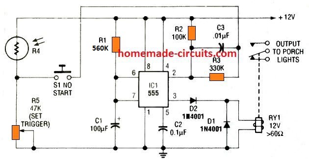 This 8th circuit shows simple porch light timer circuit that can be activated for a minute only during night time.
During day time the LDR resistance becomes low which keeps its junction with R5 high.
Due to this, pressing S1 has no effect on pin 2 of the IC.
However, when darkness falls, LDR resistance goes infinite, developing an nearly 0 V at the junction of R4 and R5.
In this condition when the switch S1 is pressed, causes a negative trigger at pin 2 of the IC 555, which activates pin 3 to high and also turns ON the relay.
The porch light attached with the relay contacts illuminates.
The circuit stays triggered for around 1 minute, until C1 charges to the 2/3rd Vcc.
The IC now resets to the turn pin 3 low and de-energizing the relay and switching OFF the porch light.
The switch S1 may be in the form of a small hidden switch near the door handle/hinge, or under the mat which activates when the owner steps on the mat.
This 8th circuit shows simple porch light timer circuit that can be activated for a minute only during night time.
During day time the LDR resistance becomes low which keeps its junction with R5 high.
Due to this, pressing S1 has no effect on pin 2 of the IC.
However, when darkness falls, LDR resistance goes infinite, developing an nearly 0 V at the junction of R4 and R5.
In this condition when the switch S1 is pressed, causes a negative trigger at pin 2 of the IC 555, which activates pin 3 to high and also turns ON the relay.
The porch light attached with the relay contacts illuminates.
The circuit stays triggered for around 1 minute, until C1 charges to the 2/3rd Vcc.
The IC now resets to the turn pin 3 low and de-energizing the relay and switching OFF the porch light.
The switch S1 may be in the form of a small hidden switch near the door handle/hinge, or under the mat which activates when the owner steps on the mat.
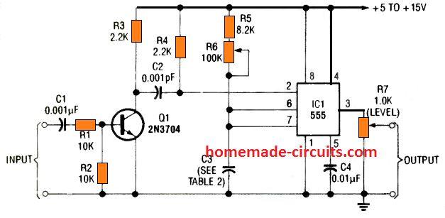
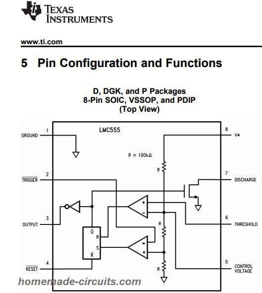 Pin#1: Ground reference voltage
Pin#2: Intended for changeover of the flip-flop through set to reset.
The output of the IC is determined by the amplitude of the external trigger pulse placed on this pin
Pin#3: Output
Pin#4: You can apply a ground or negative voltage on this pin in order disable or reset the timer function.
If not used for the resetting actions, make sure to connect the pin to VCC to enable proper triggering
Pin#5: Control voltage pin is configured to control the threshold and trigger levels.
It sets up the output waveform pulse.
You can apply an external modulating signal on this pin to modify the output PWMs
Pin#6: Analyzes the voltage applied to the pinout having a reference voltage of 2/3 Vcc.
The voltage amplitude placed on this terminal influences the set condition of the flip-flop.
Pin#7: Open collector output that discharges a timing capacitor across time intervals (in phase with output).
It alternately switches the output from high to low when voltage extends to 2/3 of the supply voltage
Pin#8: Supply voltage with respect to GND
Pin#1: Ground reference voltage
Pin#2: Intended for changeover of the flip-flop through set to reset.
The output of the IC is determined by the amplitude of the external trigger pulse placed on this pin
Pin#3: Output
Pin#4: You can apply a ground or negative voltage on this pin in order disable or reset the timer function.
If not used for the resetting actions, make sure to connect the pin to VCC to enable proper triggering
Pin#5: Control voltage pin is configured to control the threshold and trigger levels.
It sets up the output waveform pulse.
You can apply an external modulating signal on this pin to modify the output PWMs
Pin#6: Analyzes the voltage applied to the pinout having a reference voltage of 2/3 Vcc.
The voltage amplitude placed on this terminal influences the set condition of the flip-flop.
Pin#7: Open collector output that discharges a timing capacitor across time intervals (in phase with output).
It alternately switches the output from high to low when voltage extends to 2/3 of the supply voltage
Pin#8: Supply voltage with respect to GND
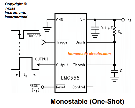 Subsequently, with no trigger signal, the voltage across the capacitor begins increasing exponentially for a time interval tH = 1.1 RAC equivalent to the time for which the output is held high, after which the voltage across the capacitor reaches 2/3rd VS.
The internal comparator responds to this change and resets the flip flop, which quickly discharges the external capacitor reverting the output at its initial low state.
Astable Operation
In the astable mode as shown in the following figure (Threshold and trigger pins shorted), the circuit goes into a self-triggering mode, in the form of a free running multivibrator.
Subsequently, with no trigger signal, the voltage across the capacitor begins increasing exponentially for a time interval tH = 1.1 RAC equivalent to the time for which the output is held high, after which the voltage across the capacitor reaches 2/3rd VS.
The internal comparator responds to this change and resets the flip flop, which quickly discharges the external capacitor reverting the output at its initial low state.
Astable Operation
In the astable mode as shown in the following figure (Threshold and trigger pins shorted), the circuit goes into a self-triggering mode, in the form of a free running multivibrator.
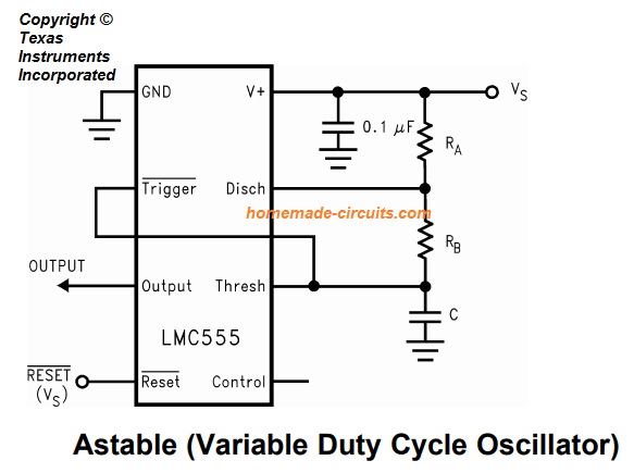 The resistor combination RA + RB , and RB alone alternately charges and discharges the timing capacitor respectively, generating a chain of continuous output rectangular waves, with a specific duty cycle.
Since the mentioned resistors control charging and discharging rate of the capacitor, implies that these resistors directly become responsible for determining the duty cycle of the output pulses, and their values can be altered appropriately for achieving the desired duty cycle.
Just like in the monostable triggered mode, here too the capacitor undergoes a charging and discharging process through the levels of 1/3 Vs and 2/3 Vs.
The resistor combination RA + RB , and RB alone alternately charges and discharges the timing capacitor respectively, generating a chain of continuous output rectangular waves, with a specific duty cycle.
Since the mentioned resistors control charging and discharging rate of the capacitor, implies that these resistors directly become responsible for determining the duty cycle of the output pulses, and their values can be altered appropriately for achieving the desired duty cycle.
Just like in the monostable triggered mode, here too the capacitor undergoes a charging and discharging process through the levels of 1/3 Vs and 2/3 Vs.
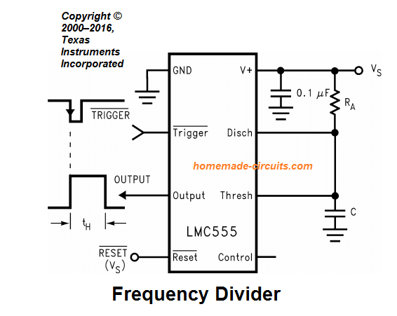 The monostable one shot configuration explained above can be implemented as a frequency divider by suitably changing the length of the timing frequency.
The following figure shows the waveforms for a divide by three configuration.
The monostable one shot configuration explained above can be implemented as a frequency divider by suitably changing the length of the timing frequency.
The following figure shows the waveforms for a divide by three configuration.
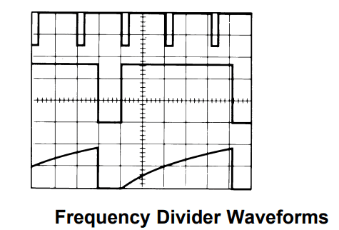 Pulse Width Modulator
The IC LMC555 can be effectively used as a Pulse Width Modulator circuit or a PWM generator circuit by suitably modifying a monostable configuration as shown below.
Pulse Width Modulator
The IC LMC555 can be effectively used as a Pulse Width Modulator circuit or a PWM generator circuit by suitably modifying a monostable configuration as shown below.
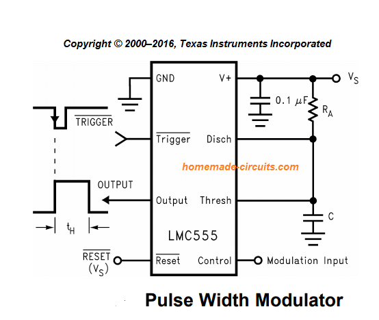 Here we can see that in the monostable mode if the trigger pin#2 is continuously triggered through an external square wave pulses, the output PWM from the IC can be modulated through a calculated signal applied at the control pin#5 of the IC.
Pulse Position Modulator
In this configuration we are able to change the position or the density of the output pulses through modulating signal yet again applied on pin#5, which is the control pin of the IC.
Here we can see that in the monostable mode if the trigger pin#2 is continuously triggered through an external square wave pulses, the output PWM from the IC can be modulated through a calculated signal applied at the control pin#5 of the IC.
Pulse Position Modulator
In this configuration we are able to change the position or the density of the output pulses through modulating signal yet again applied on pin#5, which is the control pin of the IC.
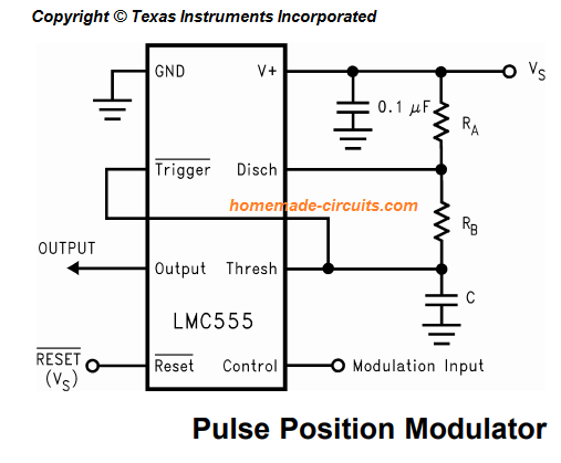 The IC is set in its astable mode, and a modulating signal s connected at the control pin of the IC, which causes the threshold voltage to vary with the signal and therefore the time delay of the PWM also vary proportionately.
The waveform image clarifies the situation below.
The IC is set in its astable mode, and a modulating signal s connected at the control pin of the IC, which causes the threshold voltage to vary with the signal and therefore the time delay of the PWM also vary proportionately.
The waveform image clarifies the situation below.
 50% Duty Cycle Oscillator
If you are looking for CMOS, TTL compatible 50% Duty Cycle Oscillator circuit, then this configuration can help to achieve the same with utmost efficiency.
The following figure shows the bare minimum required for getting the specified results.
50% Duty Cycle Oscillator
If you are looking for CMOS, TTL compatible 50% Duty Cycle Oscillator circuit, then this configuration can help to achieve the same with utmost efficiency.
The following figure shows the bare minimum required for getting the specified results.
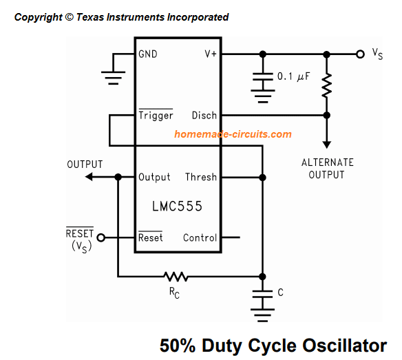 The formula for calculating the frequency is:
f = 1/(1.4 RcC)
Conclusion
LMC555 is pin on pin compatible CMOS version of our standard IC 555
The main advantage of this CMOS version is primarily extremely low power dissipation, and the minimum operational voltage range which is as low as 1.5 V.
When operated with a 5V (CV), the output becomes perfectly compatible with TTL circuits, and 74 LS based designs.
The standby current draw of this CMOS LMC555 is in uA, which is negligible compared to the normal IC 555 consumption which may be in mA.
The formula for calculating the frequency is:
f = 1/(1.4 RcC)
Conclusion
LMC555 is pin on pin compatible CMOS version of our standard IC 555
The main advantage of this CMOS version is primarily extremely low power dissipation, and the minimum operational voltage range which is as low as 1.5 V.
When operated with a 5V (CV), the output becomes perfectly compatible with TTL circuits, and 74 LS based designs.
The standby current draw of this CMOS LMC555 is in uA, which is negligible compared to the normal IC 555 consumption which may be in mA.
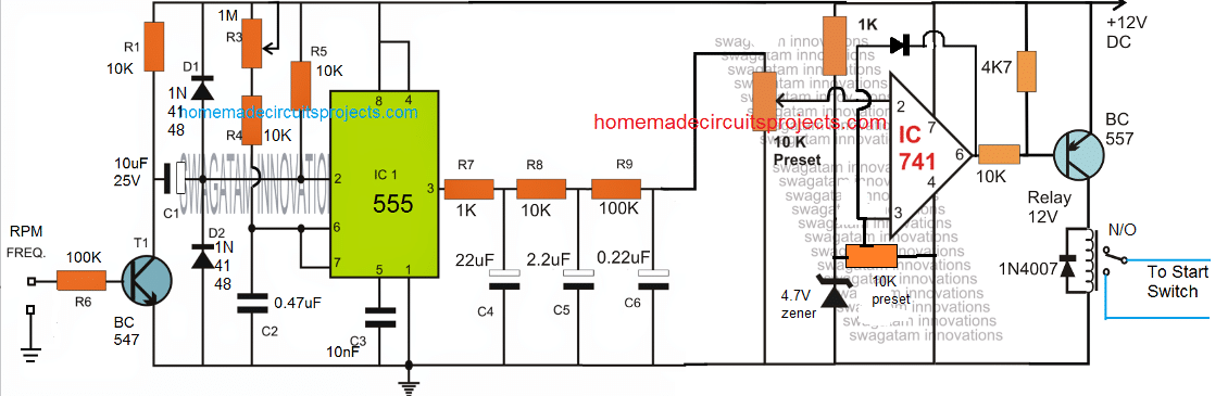 Referring to the circuit diagram of the proposed motorcycle button start lock, we can see that the design is basically divided into two stages.
The left side stage is the IC 555 based PPM generator which effectively converts the input RPM frequency signal from the vehicle's CDI into a varying pulse density output.
These varying pulse density output is fed to a 3 level RC integrator built using a few resistor and capacitor networks at pin#3 of IC 555.
The integrator smoothens the pulses from the IC555, and converts them into a steadily climbing or declining voltage, in response to the RPM frequency.
The IC 741 stage at the right side of the design is an ordinary compartaor circuit which is positioned to detect the DC levels, and activate a relay when the DC reaches a specified limit.
The 10K presets of the IC 741 are adjusted such that when the DC output corresponding to 500RPM frequency is attained from the integrator stage, pin#2 of IC 741 goes slightly higher than pin#3 potential.
When this happens, the output of the IC 741 goes low and switches ON the BJT and the relay, which in turn switches ON disconnects the starter switch from the ignition system.
The 1N4148 diode across pin#6 and pin#2 of IC741 allows the circuit to latch, so that the starter switch is held disabled permanently until the vehicle is stopped, and supply to the circuit is removed.
The pot or the preset associated with the IC 555 can be used for optimizing and achieving the best possible outcome for the RPM to DC conversion at the output of the integrator.
It is recommended that the discussed stages are tested and verified separately, and coupled together only once the stages are perfectly set and confirmed.
For any related questions please feel free to use the comment box below.
Referring to the circuit diagram of the proposed motorcycle button start lock, we can see that the design is basically divided into two stages.
The left side stage is the IC 555 based PPM generator which effectively converts the input RPM frequency signal from the vehicle's CDI into a varying pulse density output.
These varying pulse density output is fed to a 3 level RC integrator built using a few resistor and capacitor networks at pin#3 of IC 555.
The integrator smoothens the pulses from the IC555, and converts them into a steadily climbing or declining voltage, in response to the RPM frequency.
The IC 741 stage at the right side of the design is an ordinary compartaor circuit which is positioned to detect the DC levels, and activate a relay when the DC reaches a specified limit.
The 10K presets of the IC 741 are adjusted such that when the DC output corresponding to 500RPM frequency is attained from the integrator stage, pin#2 of IC 741 goes slightly higher than pin#3 potential.
When this happens, the output of the IC 741 goes low and switches ON the BJT and the relay, which in turn switches ON disconnects the starter switch from the ignition system.
The 1N4148 diode across pin#6 and pin#2 of IC741 allows the circuit to latch, so that the starter switch is held disabled permanently until the vehicle is stopped, and supply to the circuit is removed.
The pot or the preset associated with the IC 555 can be used for optimizing and achieving the best possible outcome for the RPM to DC conversion at the output of the integrator.
It is recommended that the discussed stages are tested and verified separately, and coupled together only once the stages are perfectly set and confirmed.
For any related questions please feel free to use the comment box below.
 Using a BJT Emitter Follower
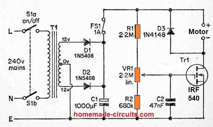 There can bea significant levelof ripple on this DC output, however it is unimportant in this application.
Tr1 provides power to the load and is biased througha resistivedivider circuit consisting of R1, VR1, and R2.
The gate bias voltage provided to Tr1 mightnot be adequate to allow the MOSFETto conduct meaningfully with the wiperof VR1 at the R2 end of its rotation, and the motor will not operate.
Advancing the wiperof VR1 towards the opposite end of its rotationallows a constantly increasing bias to be supplied to Tr1, resulting in a steadily decreasing drain to source resistance.
Because of this, the power delivered to the motor rises in tandem with the motor's speed, until Tr1 reaches saturation (wherethe motor runsat itsfull speed).
VR1 may therefore be used to change the motor's speed from minimumto maximumspeed.
C2 filters away any amount ofmains hum or other electrical noise that could otherwise be picked up by Tr1's high impedance gate circuit, preventing the motor speed from being reduced to zero.
D3 is a safety diode that inhibits any excessive reverse voltage spikes that may occur as a result of the motor's excessively inductive load.
There can bea significant levelof ripple on this DC output, however it is unimportant in this application.
Tr1 provides power to the load and is biased througha resistivedivider circuit consisting of R1, VR1, and R2.
The gate bias voltage provided to Tr1 mightnot be adequate to allow the MOSFETto conduct meaningfully with the wiperof VR1 at the R2 end of its rotation, and the motor will not operate.
Advancing the wiperof VR1 towards the opposite end of its rotationallows a constantly increasing bias to be supplied to Tr1, resulting in a steadily decreasing drain to source resistance.
Because of this, the power delivered to the motor rises in tandem with the motor's speed, until Tr1 reaches saturation (wherethe motor runsat itsfull speed).
VR1 may therefore be used to change the motor's speed from minimumto maximumspeed.
C2 filters away any amount ofmains hum or other electrical noise that could otherwise be picked up by Tr1's high impedance gate circuit, preventing the motor speed from being reduced to zero.
D3 is a safety diode that inhibits any excessive reverse voltage spikes that may occur as a result of the motor's excessively inductive load.
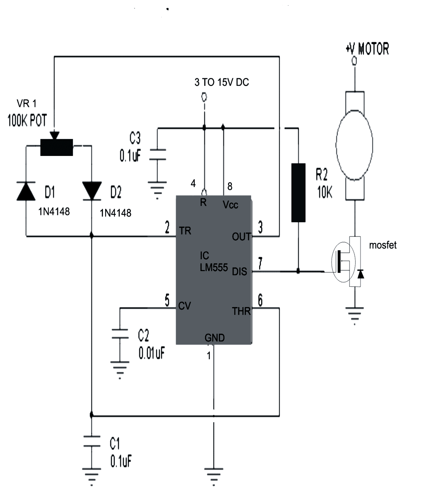
 Video Testing Proof:
In the above video clip we can see how the IC 555 based design is used for controlling speed of a DC motor.
As you may witness, although the bulb works perfectly in response to the PWMs and varies its intensity from minimum glow to maximum low, the motor does not.
The motor initially does not respond to the narrow PWMs, rather starts with a jerk after the PWMs are adjusted to significantly higher pulse widths.
This does not mean the circuit has problems, it is because the DC motor armature is held between a pair of magnets tightly.
To initiate a start the armature has to jump its rotation across the two poles of the magnet which cannot happen with a slow and gentle movement.
It has to initiate with a thrust.
That's exactly why the motor initially requires a higher adjustments for the PWM and once the rotation is initiated the armature gains some kinetic energy and now achieving slower speed becomes feasible through narrower PWMs.
However still, getting the rotation to a barely moving slow status can be impossible because of the same reason as explained above.
I tried my best to improve the response and achieve a slowest possible PWM control by making a few modifications in the first diagram as shown below:
Video Testing Proof:
In the above video clip we can see how the IC 555 based design is used for controlling speed of a DC motor.
As you may witness, although the bulb works perfectly in response to the PWMs and varies its intensity from minimum glow to maximum low, the motor does not.
The motor initially does not respond to the narrow PWMs, rather starts with a jerk after the PWMs are adjusted to significantly higher pulse widths.
This does not mean the circuit has problems, it is because the DC motor armature is held between a pair of magnets tightly.
To initiate a start the armature has to jump its rotation across the two poles of the magnet which cannot happen with a slow and gentle movement.
It has to initiate with a thrust.
That's exactly why the motor initially requires a higher adjustments for the PWM and once the rotation is initiated the armature gains some kinetic energy and now achieving slower speed becomes feasible through narrower PWMs.
However still, getting the rotation to a barely moving slow status can be impossible because of the same reason as explained above.
I tried my best to improve the response and achieve a slowest possible PWM control by making a few modifications in the first diagram as shown below:
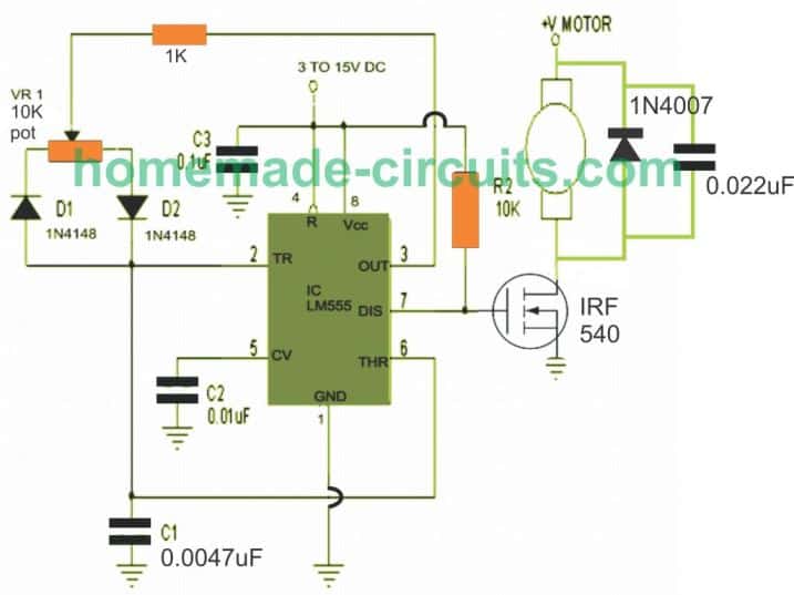 Having said this, the motor could show a better control at the slower levels if the motor is attached or strapped with a load through gears or pulley system.
This may happen because the load will act as a damper and help to provide a controlled movement during the slower speed adjustments.
Having said this, the motor could show a better control at the slower levels if the motor is attached or strapped with a load through gears or pulley system.
This may happen because the load will act as a damper and help to provide a controlled movement during the slower speed adjustments.
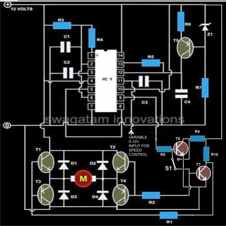
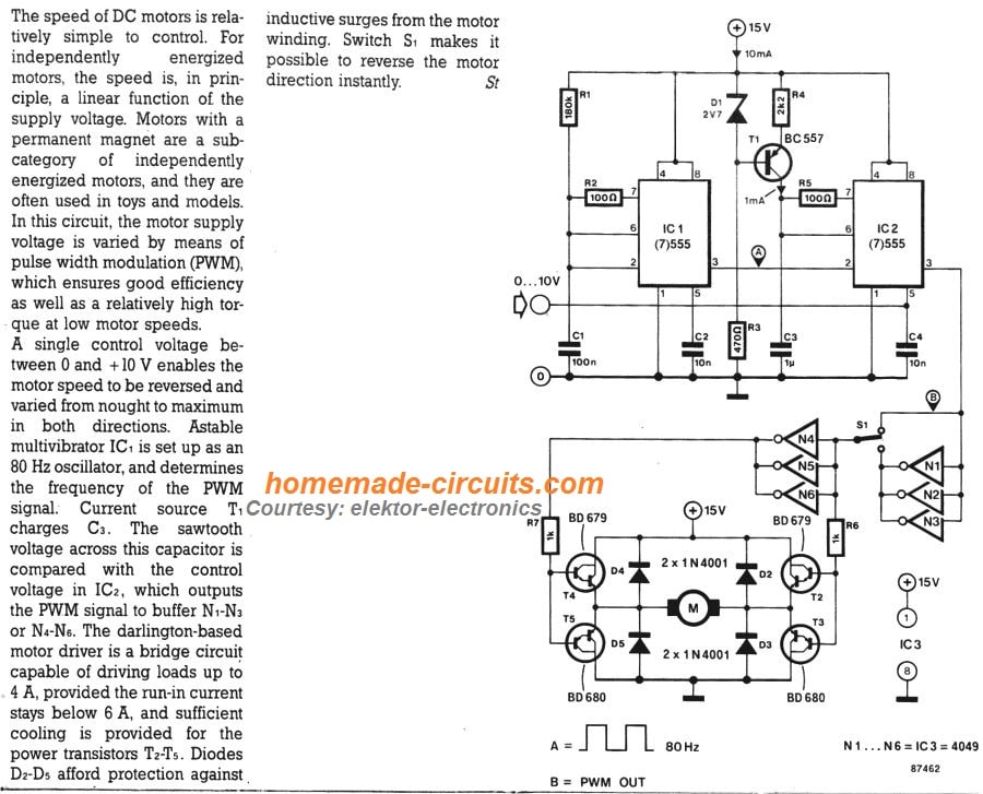 The first motor control diagram can be much simplified by using a DPDT switch for the motor reversal operation, and by using an emitter follower transistor for the speed control implementation, as shown below:
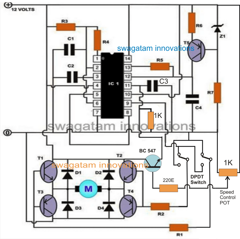
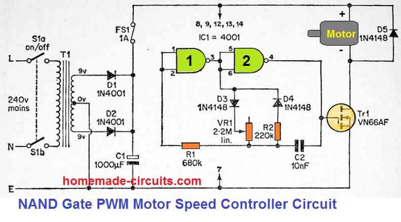 This pwm circuit is built using twoof the four gates of a CMOS 4001 device, which are utilized in a CMOS astable setup that is quite aconventional design.
A couple oftiming resistors can be seenconnected between the output of gate 1 and the junction of R1 and C2, which differs from the conventional PWMdesign.
VR1 and R2 are the two resistors, along with guidingdiodes D3 and D4 connected in series with the output of NAND gate 1.
The two diodes ensure that R2 works likethe timingresistance whenever the astable's output is high, andVR1 functions as the timing resistance whenever the output is low.
The period of the output pulses is constant since R2 has a predetermined value.
The interval between them could be changed by varyingVR1. This will benearly zero when it is adjusted for lowest resistance.
The output mark space ratio is greater than ten to one at maximum resistance.
VR1,therefore, couldbe adjusted to generate the desired motor speed with effective torque, with the lowest speed happening at full resistance and the highest speed occurring at zero resistance.
This pwm circuit is built using twoof the four gates of a CMOS 4001 device, which are utilized in a CMOS astable setup that is quite aconventional design.
A couple oftiming resistors can be seenconnected between the output of gate 1 and the junction of R1 and C2, which differs from the conventional PWMdesign.
VR1 and R2 are the two resistors, along with guidingdiodes D3 and D4 connected in series with the output of NAND gate 1.
The two diodes ensure that R2 works likethe timingresistance whenever the astable's output is high, andVR1 functions as the timing resistance whenever the output is low.
The period of the output pulses is constant since R2 has a predetermined value.
The interval between them could be changed by varyingVR1. This will benearly zero when it is adjusted for lowest resistance.
The output mark space ratio is greater than ten to one at maximum resistance.
VR1,therefore, couldbe adjusted to generate the desired motor speed with effective torque, with the lowest speed happening at full resistance and the highest speed occurring at zero resistance.
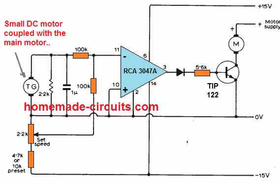 This motor controller enables infinitely adjustable range without involving any form of mechanical hassles.
The op amp output is only +/- 10% of the supply rails level, thus employing a double emitter follower huge motor speeds could be controlled.
The reference voltage could be fixed through thermistors, or an LDR etc.
The experimental set up indicated in the circuit diagram made use of an RCA 3047A op amp, and a 0.25W 6V motor as tacho-generator which generated around 4V at 13000 r.p.m for the intended feedback.
Additional Circuit Designs:
This motor controller enables infinitely adjustable range without involving any form of mechanical hassles.
The op amp output is only +/- 10% of the supply rails level, thus employing a double emitter follower huge motor speeds could be controlled.
The reference voltage could be fixed through thermistors, or an LDR etc.
The experimental set up indicated in the circuit diagram made use of an RCA 3047A op amp, and a 0.25W 6V motor as tacho-generator which generated around 4V at 13000 r.p.m for the intended feedback.
Additional Circuit Designs:
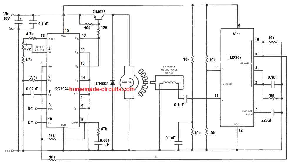 The above diagram shows a basic PWM motor control circuit using the IC LM3524. The design additionally incorporates a sensor based feedback control through the IC LM2907.
A small magnet is attached with the motor shaft, such that during the rotations, the magnet goes past closely to an iron core pickup coil transformer.
The mechanism, causes the rotating magnet to induce a sharp electrical pulse in the pickup coil, which is used by the LM2907 as a trigger input and appropriately processed as the feedback control pulse to the LM3524 IC.
The feedback system ensures that the speed of the once set can never deviate from the set point, providing a precise control of the speed.
The pot at pin#2 of the LM3524 is used for controlling the speed of the motor.
The above diagram shows a basic PWM motor control circuit using the IC LM3524. The design additionally incorporates a sensor based feedback control through the IC LM2907.
A small magnet is attached with the motor shaft, such that during the rotations, the magnet goes past closely to an iron core pickup coil transformer.
The mechanism, causes the rotating magnet to induce a sharp electrical pulse in the pickup coil, which is used by the LM2907 as a trigger input and appropriately processed as the feedback control pulse to the LM3524 IC.
The feedback system ensures that the speed of the once set can never deviate from the set point, providing a precise control of the speed.
The pot at pin#2 of the LM3524 is used for controlling the speed of the motor.
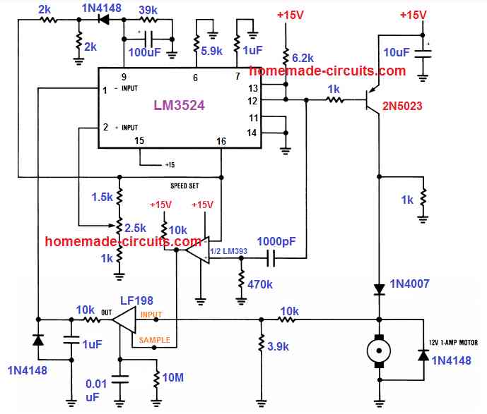 Here, the back EMF from the motor is utilized as the feedback signal and applied to the input of the IC LF198. In case the speed tends to rise beyond the set level, the LF198 compares the rising EMF signal with the sample reference signal from the LM393 output.
The resulting output is sent to the error amplifier of the IC LM3524 for the necessary processing of the output PWM to the driver transistors.
The controlled PWM due to this sensor-less feedback through the back EMF ultimately enables the motor to remain precisely fixed at a correct speed, as adjusted by the pin#2 potentiometer.
Here, the back EMF from the motor is utilized as the feedback signal and applied to the input of the IC LF198. In case the speed tends to rise beyond the set level, the LF198 compares the rising EMF signal with the sample reference signal from the LM393 output.
The resulting output is sent to the error amplifier of the IC LM3524 for the necessary processing of the output PWM to the driver transistors.
The controlled PWM due to this sensor-less feedback through the back EMF ultimately enables the motor to remain precisely fixed at a correct speed, as adjusted by the pin#2 potentiometer.
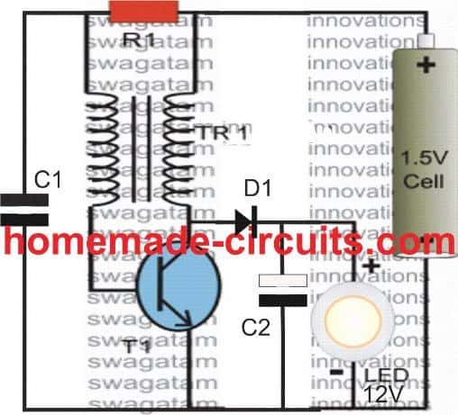 Parts List
R1 = 1K 1/4 watt
D1 = 1N4148 or aSchottkydiode such as FR107 or BA159
T1 = any NPN power BJT such as TIP31, 2N2222, 8050 or BC139 (on heatsink)
C1 = 0.0047uF
C2 = 1000uF/25V
Inductor = 20 turns each of super enameled copper wire on a ferrite torroid T13. Wire thickness can be as per the output current requirement.
Parts List
R1 = 1K 1/4 watt
D1 = 1N4148 or aSchottkydiode such as FR107 or BA159
T1 = any NPN power BJT such as TIP31, 2N2222, 8050 or BC139 (on heatsink)
C1 = 0.0047uF
C2 = 1000uF/25V
Inductor = 20 turns each of super enameled copper wire on a ferrite torroid T13. Wire thickness can be as per the output current requirement.
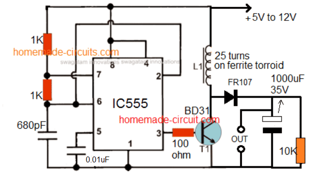 The above circuit can be regulated with a feedback as shown below:
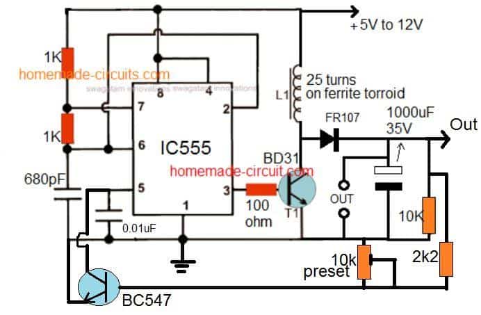 The idea looks quite straightforward.
IC 555 is configured as an astable multivibratorwhose frequency is decided by the values of resistors and capacitor at pin#7 and pin#6/2.
This frequency is applied to the base of a driver transistor TIP31 (incorrectly shown as BD31).
The transistor oscillates at the same frequency and forces supply current to oscillate within the connected inductor with the same frequency.
The selected frequency saturates the coil and boosts the voltage across it to a greater amplitude which is measured to be around 24V.
This value can be tweaked to even higher levels by modifying the turns of the inductor and the frequency of the IC .
Video Links for the above boost converter circuits are provided below:
The idea looks quite straightforward.
IC 555 is configured as an astable multivibratorwhose frequency is decided by the values of resistors and capacitor at pin#7 and pin#6/2.
This frequency is applied to the base of a driver transistor TIP31 (incorrectly shown as BD31).
The transistor oscillates at the same frequency and forces supply current to oscillate within the connected inductor with the same frequency.
The selected frequency saturates the coil and boosts the voltage across it to a greater amplitude which is measured to be around 24V.
This value can be tweaked to even higher levels by modifying the turns of the inductor and the frequency of the IC .
Video Links for the above boost converter circuits are provided below:
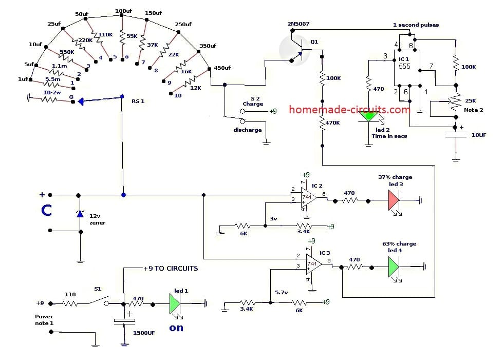 The 12 volt zener is also for voltage protection.
If the capacitor is polarity marked, the red dot, or + should be connected to the positive test lead.
The selector switch should also be in position ��G�� when connecting.
S2 should be in ��discharge�� position.
The rotary switch resistor sizes were determine by inverting the formula T=RC, so that R=T/C.
Each value of resistor on the rotary switch is selected to provides an approximate time of 5.5 seconds to charge.
The actual average charge time takes 4.5 to 6.5 seconds.
Resistor tolerances and slight differences in capacitor values create the difference in the 5.5 second design.
The supply voltage needs to be very close to 9 volts.
Any lower, or higher voltage will effect the voltage at the resistance dividers at IC 2 and IC 3 input pins 3.
The 12 volt zener is also for voltage protection.
If the capacitor is polarity marked, the red dot, or + should be connected to the positive test lead.
The selector switch should also be in position ��G�� when connecting.
S2 should be in ��discharge�� position.
The rotary switch resistor sizes were determine by inverting the formula T=RC, so that R=T/C.
Each value of resistor on the rotary switch is selected to provides an approximate time of 5.5 seconds to charge.
The actual average charge time takes 4.5 to 6.5 seconds.
Resistor tolerances and slight differences in capacitor values create the difference in the 5.5 second design.
The supply voltage needs to be very close to 9 volts.
Any lower, or higher voltage will effect the voltage at the resistance dividers at IC 2 and IC 3 input pins 3.
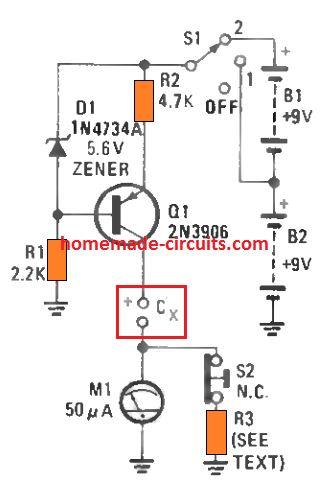 A dual-range metering circuit is employed to display the capacitor's charge and leakage current.
A couple of batteries supply power to the circuit.
A 5 V Zener diode (D1) fixes the Q1's base at a constant 5 V potential, ensuring a constant voltage drop around R2 (Q1's emitter resistor) and a constant current on the capacitor under test (shown as Cx).
When set at the S1 position 1, the voltage used on Cx is restricted to around 4 V; having S1 in position 2, the voltage over the capacitor increases to around 12 V.
An additional battery could be included in series with B1 and B2 to enhance the charging voltage to approximately 20 V.
With S2 in its normally closed position (as demonstrated), the meter gets wired in parallel with R3 (the meter's shunt resistor), allowing the circuit with a full-scale display of 1 mA.
When S2 is depressed (open), the metering range of the circuit is lowered to 50 uA full scale.
A dual-range metering circuit is employed to display the capacitor's charge and leakage current.
A couple of batteries supply power to the circuit.
A 5 V Zener diode (D1) fixes the Q1's base at a constant 5 V potential, ensuring a constant voltage drop around R2 (Q1's emitter resistor) and a constant current on the capacitor under test (shown as Cx).
When set at the S1 position 1, the voltage used on Cx is restricted to around 4 V; having S1 in position 2, the voltage over the capacitor increases to around 12 V.
An additional battery could be included in series with B1 and B2 to enhance the charging voltage to approximately 20 V.
With S2 in its normally closed position (as demonstrated), the meter gets wired in parallel with R3 (the meter's shunt resistor), allowing the circuit with a full-scale display of 1 mA.
When S2 is depressed (open), the metering range of the circuit is lowered to 50 uA full scale.
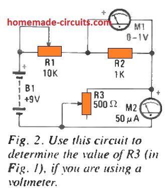 In this procedure, adjust R1 (the 10k potentiometer) to its highest resistance and adjust R3 (the 500-ohm potentiometer) to its lowest magnitude.
Attach a battery as indicated and fine-tune R1 for getting a 1 V reading on M1. Carefully increase the R3 preset value until M2 (the current meter) displays a full scale deflection.
Examine only R1 while you alter R3 preset to maintain a 1V reading on M1.
While M1 indicates 1 volt and M2 displays full scale, the potentiometer is established at the right resistance value necessary for R3. You may either work with a potentiometer for the shunt resistor or choose one of equivalent value out of your resistor box.
Alternatively, if you have a precision ammeter which can check 1 mA, you cam try the circuit in Fig.
3.
In this procedure, adjust R1 (the 10k potentiometer) to its highest resistance and adjust R3 (the 500-ohm potentiometer) to its lowest magnitude.
Attach a battery as indicated and fine-tune R1 for getting a 1 V reading on M1. Carefully increase the R3 preset value until M2 (the current meter) displays a full scale deflection.
Examine only R1 while you alter R3 preset to maintain a 1V reading on M1.
While M1 indicates 1 volt and M2 displays full scale, the potentiometer is established at the right resistance value necessary for R3. You may either work with a potentiometer for the shunt resistor or choose one of equivalent value out of your resistor box.
Alternatively, if you have a precision ammeter which can check 1 mA, you cam try the circuit in Fig.
3.
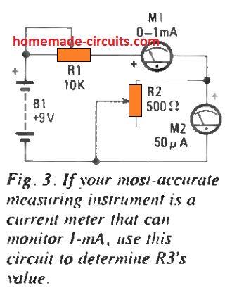 You can implement exactly the same procedures as done for Fig.
2 and fine-tune the R1 for a 1 mA display.
You can implement exactly the same procedures as done for Fig.
2 and fine-tune the R1 for a 1 mA display.

 Joysticks are electronic devices in general so, we need to apply power.
The movement of the lever produces voltage difference at output pins.
The voltage levels are processed by a microcontroller to control the output device such as a motor.
The illustrated joystick is similar one, which can be found in PlayStation and Xbox controllers.
You no need to break these controllers to salvage one.
These modules are readily available at local electronic shops and E-commerce sites.
Now let��s see the construction of this joystick.
It has two 10 Kilo ohm potentiometer positioned in X and Y axes with springs so that, it returns to its original position when the user release force from the lever.
It has a push to ON button on Z axis.
It has 5 pins, 5 volt Vcc, GND, variable X, variable Y, and SW (Z axis switch).
When we apply voltage and left the joystick on its original lever position.
The X and Y pins will produce half of the applied voltage.
When we move the lever the voltage varies in X and Y output pins.
Now let��s practically interface the joystick to Arduino.
Joysticks are electronic devices in general so, we need to apply power.
The movement of the lever produces voltage difference at output pins.
The voltage levels are processed by a microcontroller to control the output device such as a motor.
The illustrated joystick is similar one, which can be found in PlayStation and Xbox controllers.
You no need to break these controllers to salvage one.
These modules are readily available at local electronic shops and E-commerce sites.
Now let��s see the construction of this joystick.
It has two 10 Kilo ohm potentiometer positioned in X and Y axes with springs so that, it returns to its original position when the user release force from the lever.
It has a push to ON button on Z axis.
It has 5 pins, 5 volt Vcc, GND, variable X, variable Y, and SW (Z axis switch).
When we apply voltage and left the joystick on its original lever position.
The X and Y pins will produce half of the applied voltage.
When we move the lever the voltage varies in X and Y output pins.
Now let��s practically interface the joystick to Arduino.
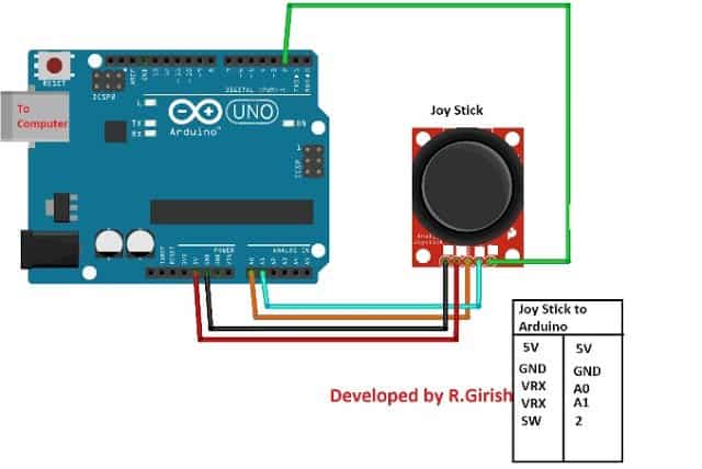 The pin connection details are given beside the circuit.
Connect the completed hardware setup and upload the code.
The pin connection details are given beside the circuit.
Connect the completed hardware setup and upload the code.
 These X, Y, Z axes values are used to interpret the position of the lever.
As you can see the values are from 0 to 1023.
That��s because Arduino has built in ADC converter which convert the voltage 0V - 5V to 0 to 1023 values.
You can witness from the serial monitor that when the lever is left untouched the lever stays at mid position of both X and Y axes and shows half value of 1023.
You can also see it is not exact half of the 1023 that��s because manufacturing these joysticks never been perfect.
By now, you would have got some technical knowledge about joysticks.
Now let��s see how to control two servo motors using one joystick.
These X, Y, Z axes values are used to interpret the position of the lever.
As you can see the values are from 0 to 1023.
That��s because Arduino has built in ADC converter which convert the voltage 0V - 5V to 0 to 1023 values.
You can witness from the serial monitor that when the lever is left untouched the lever stays at mid position of both X and Y axes and shows half value of 1023.
You can also see it is not exact half of the 1023 that��s because manufacturing these joysticks never been perfect.
By now, you would have got some technical knowledge about joysticks.
Now let��s see how to control two servo motors using one joystick.
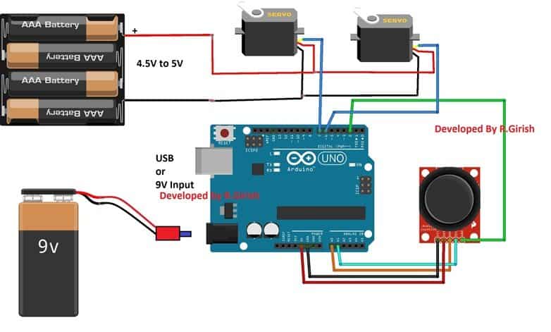 The two servo motors are controlled by one joystick; when you move the joystick along the X axis the servo connected at pin #7 moves Clockwise and Anti-clock wise depending on the lever position.
You can also hold the servo actuator at a position, if you hold the joystick level at a particular position.
Similar for servo motor connected at pin #6, you can move the lever along Y axis.
When you press the lever along the Z axis, the two motors will perform 180 degree sweep.
You can either connect the arduino to 9v battery or to computer.
If you connect the Arduino to computer you can open serial monitor and see the angle of the servo actuators and voltage levels.
The two servo motors are controlled by one joystick; when you move the joystick along the X axis the servo connected at pin #7 moves Clockwise and Anti-clock wise depending on the lever position.
You can also hold the servo actuator at a position, if you hold the joystick level at a particular position.
Similar for servo motor connected at pin #6, you can move the lever along Y axis.
When you press the lever along the Z axis, the two motors will perform 180 degree sweep.
You can either connect the arduino to 9v battery or to computer.
If you connect the Arduino to computer you can open serial monitor and see the angle of the servo actuators and voltage levels.
 It has 125 channels, it has maximum data rate of 2MBps and it has theoretical maximum range of 100 meters.
You will need two such modules to establish a communication link.
It has 125 channels, it has maximum data rate of 2MBps and it has theoretical maximum range of 100 meters.
You will need two such modules to establish a communication link.
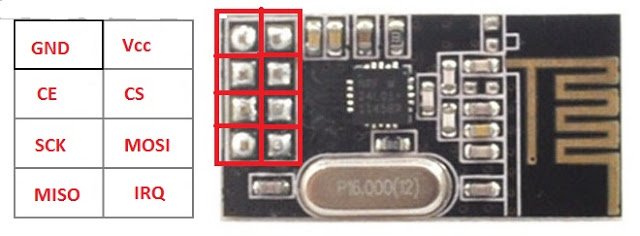 It works on SPI communication protocol.
You need to connect 7 of the 8 pins to Arduino to make this module work.
It works on 3.3 V and 5V kills the module so care must be taken while powering.
Fortunately we have on board 3.3V voltage regulator on Arduino and it must be powered only from 3.3V socket of Arduino.
Now let��s move on to Transmitter circuit.
Transmitter Circuit:
It works on SPI communication protocol.
You need to connect 7 of the 8 pins to Arduino to make this module work.
It works on 3.3 V and 5V kills the module so care must be taken while powering.
Fortunately we have on board 3.3V voltage regulator on Arduino and it must be powered only from 3.3V socket of Arduino.
Now let��s move on to Transmitter circuit.
Transmitter Circuit:
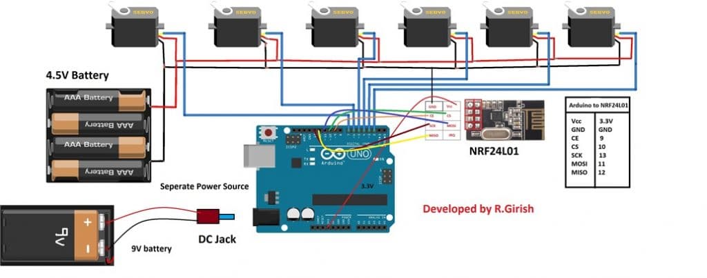 The receiver circuit consists of 6 servo motors, one Arduino and two separate power supply.
The servo motors need higher current to operate so it must not be powered from arduino.
That��s why we need two separate power source.
Please apply voltage to servo appropriately; for micro servo motors 4.8V is enough, if you want to power bulkier servo motors, apply voltage matching to the rating of servo.
Please remember that servo motor consumes some power even when there is no moment, that��s because the arm of the servo motor always fight against any change from its commented position.
The receiver circuit consists of 6 servo motors, one Arduino and two separate power supply.
The servo motors need higher current to operate so it must not be powered from arduino.
That��s why we need two separate power source.
Please apply voltage to servo appropriately; for micro servo motors 4.8V is enough, if you want to power bulkier servo motors, apply voltage matching to the rating of servo.
Please remember that servo motor consumes some power even when there is no moment, that��s because the arm of the servo motor always fight against any change from its commented position.
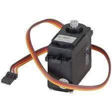

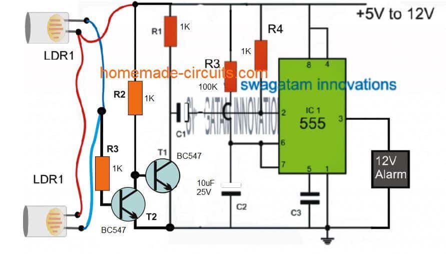
 IC 555Pinouts

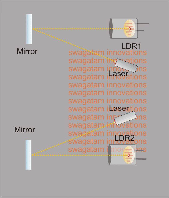
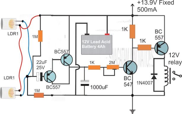
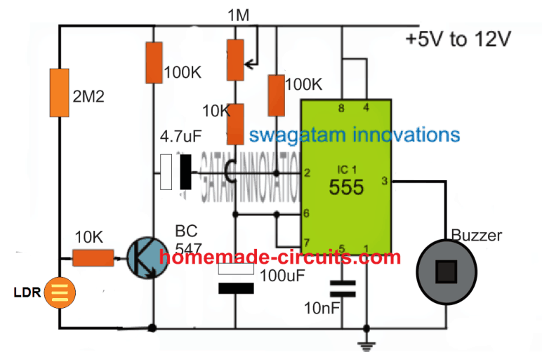
 Referring to circuit diagram it is seen that a TL072 op-amp (IC1.A) is configured as a voltage comparator, placed in between the adjustable voltage driver P1/R4 and the light-dependent voltage which consists of photodiode D1 and R3 �C a fixed resistor.
As the laser beam receives an interruption from a foreign agent, the beam is cut-off causing the voltage on comparator pin 2 to drop below pin 3, This instantly enables the output of the op amp to swing to positive voltage supply and enable an alarm situation.
As the laser alarm can detect interruption from any element, so the alarm needs to be set in a more sophisticated fashion, so that it is able to bypass accidental interrupts from elements, like an insect.
This is accomplished as the Resistor R2 provides a level of hysteresis, thereby prevent oscillation when two comparator input voltage rests in almost equal state.
Much faster response can be achieved by reducing the value of C1 to 1 ��F.
Referring to circuit diagram it is seen that a TL072 op-amp (IC1.A) is configured as a voltage comparator, placed in between the adjustable voltage driver P1/R4 and the light-dependent voltage which consists of photodiode D1 and R3 �C a fixed resistor.
As the laser beam receives an interruption from a foreign agent, the beam is cut-off causing the voltage on comparator pin 2 to drop below pin 3, This instantly enables the output of the op amp to swing to positive voltage supply and enable an alarm situation.
As the laser alarm can detect interruption from any element, so the alarm needs to be set in a more sophisticated fashion, so that it is able to bypass accidental interrupts from elements, like an insect.
This is accomplished as the Resistor R2 provides a level of hysteresis, thereby prevent oscillation when two comparator input voltage rests in almost equal state.
Much faster response can be achieved by reducing the value of C1 to 1 ��F.
 Consider the circuit shown below, driven by a 6 volt rechargeable battery.
The load may include LEDs along with resistors or amoureux lamps; you may possibly have a 22 excellent candlestick light effect by operating 12V volt lamps on 6 volts.
Consider the circuit shown below, driven by a 6 volt rechargeable battery.
The load may include LEDs along with resistors or amoureux lamps; you may possibly have a 22 excellent candlestick light effect by operating 12V volt lamps on 6 volts.
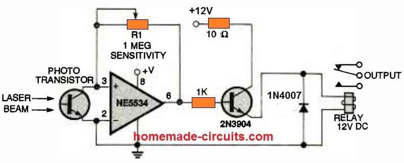 Unmonitored chambers could also be "watched" for suspicious smokes, which could indicate a fire.
Point the laser, either wholly or partly, at the high-gain relay, and set the sensitivity setting, R1, to just enable the triggering of the relay contacts.
Adjust back the preset just slightlyenough to allow the relay to reopen.
If smoke enters the path between the beam and the detector, it causes the relay to energize and activate the alarm.
Unmonitored chambers could also be "watched" for suspicious smokes, which could indicate a fire.
Point the laser, either wholly or partly, at the high-gain relay, and set the sensitivity setting, R1, to just enable the triggering of the relay contacts.
Adjust back the preset just slightlyenough to allow the relay to reopen.
If smoke enters the path between the beam and the detector, it causes the relay to energize and activate the alarm.

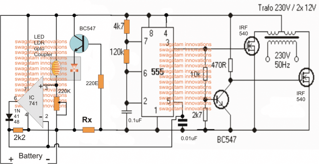 The IC 555 along with the associated mosfets and transformer forms a decent inverter circuitfor driving the specified single phase induction motor from a 12V or a 24V battery.
For a 24V battery the IC section will need to be stepped
down to 12V through a suitable voltage regulator stage.
Coming back to the actual design, here we need to make sure that the induction motor connected with the transformer initiates with a lower speed and begins gaining momentum, speed and torque as it gets loaded.
The IC 555 along with the associated mosfets and transformer forms a decent inverter circuitfor driving the specified single phase induction motor from a 12V or a 24V battery.
For a 24V battery the IC section will need to be stepped
down to 12V through a suitable voltage regulator stage.
Coming back to the actual design, here we need to make sure that the induction motor connected with the transformer initiates with a lower speed and begins gaining momentum, speed and torque as it gets loaded.
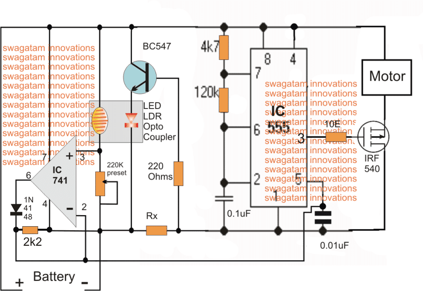 I am sure you would be having many concerned questions, so please feel freeto put them forth through your valuable comments.
All your related queries will be answered at an earliest
I am sure you would be having many concerned questions, so please feel freeto put them forth through your valuable comments.
All your related queries will be answered at an earliest
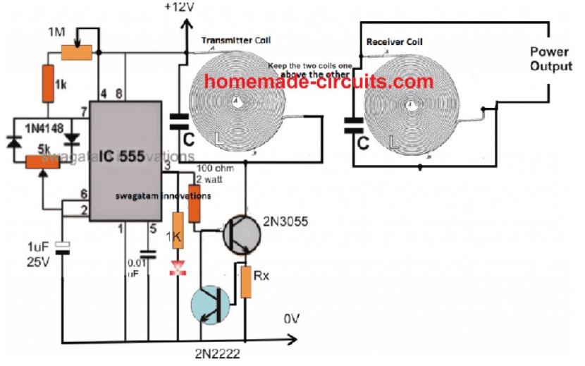 The 2N2222 transistor is introduced to make sure that while adjusting the resonance, the 2N3055 is never subjected to an over current situation.
In case this tends to happen the over current develops an equivalent amount of triggering across Rx sufficient to activate the 2N2222, which in turn shorts the 2N3055 base to ground inhibiting it from conducting any further and thus preventing the device from a possible damage.
Rx may be calculated using the following formula:
Rx = 0.6/Max current Limit of the transistor (or the wireless power transfer)
The 2N2222 transistor is introduced to make sure that while adjusting the resonance, the 2N3055 is never subjected to an over current situation.
In case this tends to happen the over current develops an equivalent amount of triggering across Rx sufficient to activate the 2N2222, which in turn shorts the 2N3055 base to ground inhibiting it from conducting any further and thus preventing the device from a possible damage.
Rx may be calculated using the following formula:
Rx = 0.6/Max current Limit of the transistor (or the wireless power transfer)
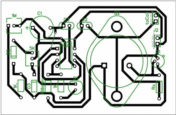
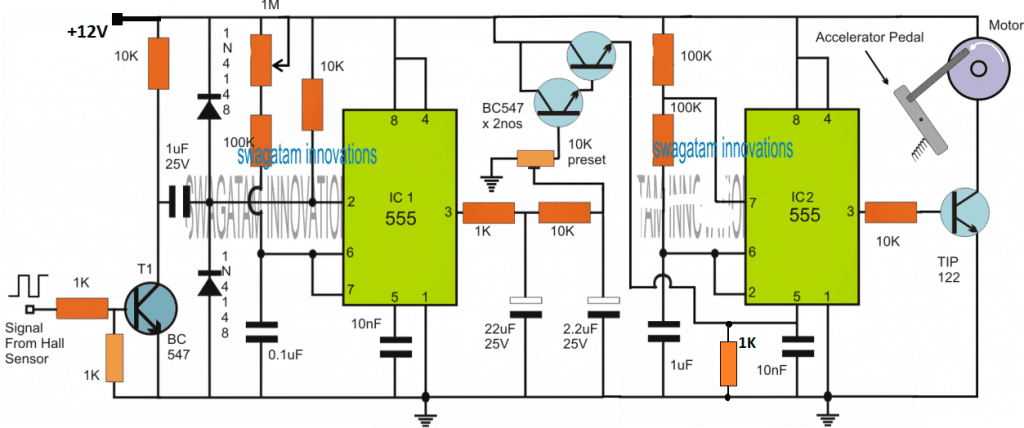 NOTE: THE MOTOR COULD BE REPLACED WITH A 12 V SPRING LOADED SOLENOID
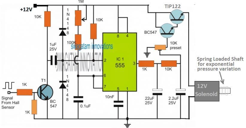 The solenoid shaft could be coupled with the accelerator pedal for accomplishing the intended automatic engine speed regulation.
For more options regarding frequency to voltage converter, you can refer to the this article.
The solenoid shaft could be coupled with the accelerator pedal for accomplishing the intended automatic engine speed regulation.
For more options regarding frequency to voltage converter, you can refer to the this article.
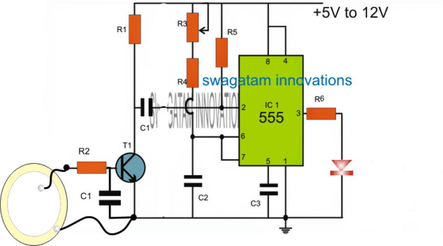

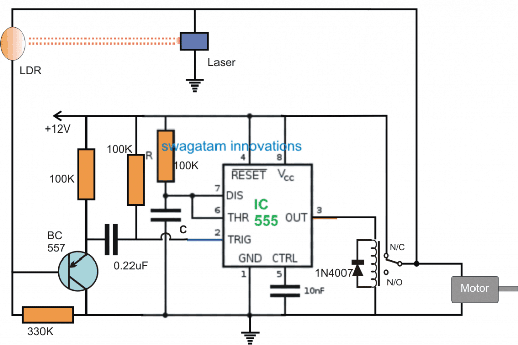 The functioning of the circuit can be understood as given below:
When power is first switched ON, the supply powers the 555 circuit and simultaneously also switches ON the motor, and the laser through the relay N/C contacts causing a low resistance on the receiving LDR device.
The low resistance from the LDR inhibits the BC557 from conducting and the situation locks in this condition, until the space between the Laser/LDR begins filling with the relevant material.
As the material begins filling, at some point of time it reaches the threshold level between the LDR/laser communication beam, and interrupts the beam.
As soon as this happens, the LDR resistance becomes high allowing the BC557 to conduct and trigger the IC 555 stage which is actually wired as a standard monostable multivibrator circuit.
The IC 555 triggers into action and in the course activates the relay.
The relay contacts change position from N/C to N/O, which instantly cuts-off power to the laser and LDR network and the motor, as requested by the user.
The situation is sustained until the set time of the monostable lapses and the relay reverts to its earlier N/C position.
The circuit now attains its original standby position and activates the motor, until the storage is full again.
The proposed material storage level controller circuit can be further enhanced with an alarm indication by suitably attaching a 12V alarm circuit with the N/O contact of the relay so that whenever the storage is full, the relay disables the laser and also activates the associated alarm.
The value of C can be determined with respect to the 100k resistor from this IC 555 calculator software.
The functioning of the circuit can be understood as given below:
When power is first switched ON, the supply powers the 555 circuit and simultaneously also switches ON the motor, and the laser through the relay N/C contacts causing a low resistance on the receiving LDR device.
The low resistance from the LDR inhibits the BC557 from conducting and the situation locks in this condition, until the space between the Laser/LDR begins filling with the relevant material.
As the material begins filling, at some point of time it reaches the threshold level between the LDR/laser communication beam, and interrupts the beam.
As soon as this happens, the LDR resistance becomes high allowing the BC557 to conduct and trigger the IC 555 stage which is actually wired as a standard monostable multivibrator circuit.
The IC 555 triggers into action and in the course activates the relay.
The relay contacts change position from N/C to N/O, which instantly cuts-off power to the laser and LDR network and the motor, as requested by the user.
The situation is sustained until the set time of the monostable lapses and the relay reverts to its earlier N/C position.
The circuit now attains its original standby position and activates the motor, until the storage is full again.
The proposed material storage level controller circuit can be further enhanced with an alarm indication by suitably attaching a 12V alarm circuit with the N/O contact of the relay so that whenever the storage is full, the relay disables the laser and also activates the associated alarm.
The value of C can be determined with respect to the 100k resistor from this IC 555 calculator software.

 Referring to the figure above, the left side IC 555 is configured as a bistable for enabling the required push-button operated ON/OFF actions.
The "SET" button initiates the IC 555 and causes a high logic to appear at its pin#3, while the "RESET" button deactivates the IC operation and switches OFF pin#3 logic to a zero.
In the activated mode the bistable stage powers the right side IC 555 stage which is wired as a standard astable circuit for generating a flashing or blinking output at its pin#3 which in turn causes the attached red LEDs to light up with a rapid flashing effect, simulating a strobing light.
The strobing rate can be controlled through the 100k pot associated with the astable IC 555 stage.
Along with the activation of the the strobing lights, the bistable stage also triggers and illuminates a power LED via a driver transistor TIP122, so that the crosswalk could be illuminated with sufficient light for the user.
Once the user has crossed the path, pressing the RESET button toggles off the whole system until the SET button is pressed yet again by some other pedestrian.
In order to make the system self contained, this illuminated crosswalk safety circuit employs an appropriately rated solar panel and a compatible 12V rechargeable battery for powering the circuit and the LeDs.
During day time the battery is charged, and when darkness sets in, the battery reverts its power for the intended crosswalk safety light operations.
The battery and the panel specifications will depend on the type of LEDs used for the purpose.
The emitter-follower transistor configuration attached with the solar panel ensures a controlled charging for the battery and never allows it charge over a predetermined level, as set by its base zener diode.
Referring to the figure above, the left side IC 555 is configured as a bistable for enabling the required push-button operated ON/OFF actions.
The "SET" button initiates the IC 555 and causes a high logic to appear at its pin#3, while the "RESET" button deactivates the IC operation and switches OFF pin#3 logic to a zero.
In the activated mode the bistable stage powers the right side IC 555 stage which is wired as a standard astable circuit for generating a flashing or blinking output at its pin#3 which in turn causes the attached red LEDs to light up with a rapid flashing effect, simulating a strobing light.
The strobing rate can be controlled through the 100k pot associated with the astable IC 555 stage.
Along with the activation of the the strobing lights, the bistable stage also triggers and illuminates a power LED via a driver transistor TIP122, so that the crosswalk could be illuminated with sufficient light for the user.
Once the user has crossed the path, pressing the RESET button toggles off the whole system until the SET button is pressed yet again by some other pedestrian.
In order to make the system self contained, this illuminated crosswalk safety circuit employs an appropriately rated solar panel and a compatible 12V rechargeable battery for powering the circuit and the LeDs.
During day time the battery is charged, and when darkness sets in, the battery reverts its power for the intended crosswalk safety light operations.
The battery and the panel specifications will depend on the type of LEDs used for the purpose.
The emitter-follower transistor configuration attached with the solar panel ensures a controlled charging for the battery and never allows it charge over a predetermined level, as set by its base zener diode.
 NOTE: Please replace the 1 nF capacitor with a 0.47 uF capacitor for optimizing 50 Hz at the output.
It can be a polar or a non-polar.
NOTE: Please replace the 1 nF capacitor with a 0.47 uF capacitor for optimizing 50 Hz at the output.
It can be a polar or a non-polar.
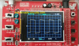
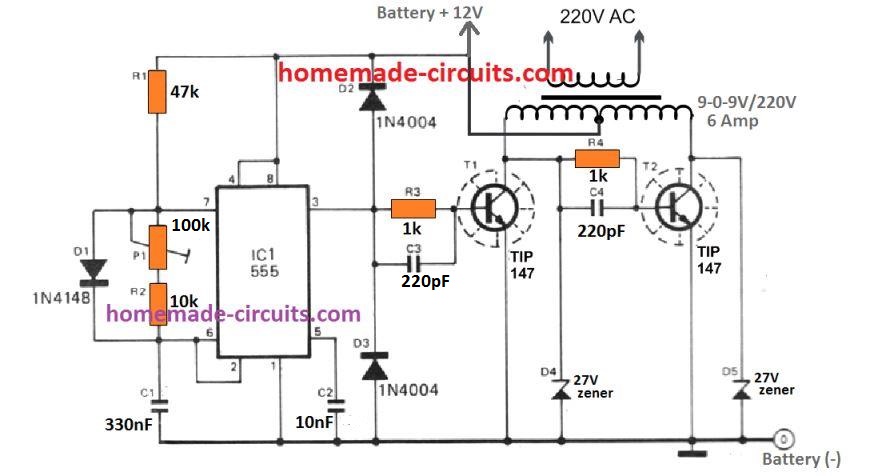 NOTE: The transistors are wrongly shown as TIP147, which are actually TIP142
UPDATE: Did you know, you could make a cool modified sine wave inverter simply by combining a IC 555 with IC 4017, see the second diagram from this article: Recommended for all dedicated inverter hobbyists
NOTE: The transistors are wrongly shown as TIP147, which are actually TIP142
UPDATE: Did you know, you could make a cool modified sine wave inverter simply by combining a IC 555 with IC 4017, see the second diagram from this article: Recommended for all dedicated inverter hobbyists
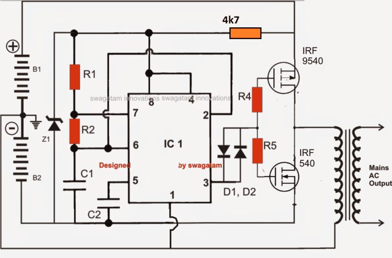
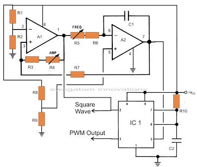 The circuit diagram can be understood with the following points:
The two opamps are basically arranged to generate the required sample source voltages for the IC 555.
The couple of outputs from this stage is responsible for the generation of square waves and triangular waves.
The second stage which is actually the heart of the circuit consists of the IC 555.
Here the IC is wired in a monostable mode with the square waves from the opamp stage applied to its trigger pin #2 and the triangular waves applied to its control voltage pin # 5.
The square wave input triggers the monostable to generate a chain of pulses at the output where as the triangular signal modulates the width of this output square wave pulses.
The output from the IC 555 now follows the ��instructions�� from the opamp stage and optimizes its output in response to the two input signals, producing the sine equivalent PWM pulses.
Now it��s just a matter of appropriately feeding the PWM pulses to the output stages of an inverter consisting of the output devices, the transformer and the battery.
The circuit diagram can be understood with the following points:
The two opamps are basically arranged to generate the required sample source voltages for the IC 555.
The couple of outputs from this stage is responsible for the generation of square waves and triangular waves.
The second stage which is actually the heart of the circuit consists of the IC 555.
Here the IC is wired in a monostable mode with the square waves from the opamp stage applied to its trigger pin #2 and the triangular waves applied to its control voltage pin # 5.
The square wave input triggers the monostable to generate a chain of pulses at the output where as the triangular signal modulates the width of this output square wave pulses.
The output from the IC 555 now follows the ��instructions�� from the opamp stage and optimizes its output in response to the two input signals, producing the sine equivalent PWM pulses.
Now it��s just a matter of appropriately feeding the PWM pulses to the output stages of an inverter consisting of the output devices, the transformer and the battery.
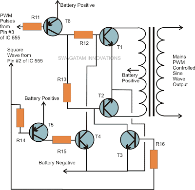 The above PWM output is applied to the output stage as shown in the figure.
Transistors T1 and T2 receive the PWM pulses at their bases and switch the battery voltage into the transformer winding according to the duty cycles of the PWM optimized waveform.
The other two transistors make sure that the conduction of T1 and T2 takes place in tandem, that is alternately so tat the output o from the transformer generates one complete AC cycle with the two halves of the PWM pulses.
The above PWM output is applied to the output stage as shown in the figure.
Transistors T1 and T2 receive the PWM pulses at their bases and switch the battery voltage into the transformer winding according to the duty cycles of the PWM optimized waveform.
The other two transistors make sure that the conduction of T1 and T2 takes place in tandem, that is alternately so tat the output o from the transformer generates one complete AC cycle with the two halves of the PWM pulses.
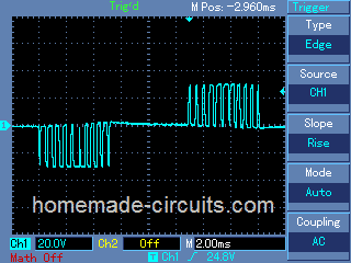 (Courtesy: Mr.
Robin Peter)
Please also see this500 VA modified sine wave design, developed by me.
Parts List for the above IC 555 pure sine wave inverter circuit
R1, R2, R3, R8, R9, R10 = 10K,
R7 = 8K2,
R11, R14, R15, R16 = 1K,
R12, R13 = 33 Ohms 5 Watt,
R4 = 1M preset,
R5 = 150 K preset,
R6 = 1K5
C1 = 0.1 uF,
C2 = 100 pF,
IC1 = TL 072,
IC2 = 555,
T1, T2 = BDY29,
T5, T6 = TIP 127,
T3, T4 = TIP122
Transformer = 12 �C 0 �C 12 V, 200 Watts,
Battery = 12 volts, 100 AH.
IC 555 Pinout
(Courtesy: Mr.
Robin Peter)
Please also see this500 VA modified sine wave design, developed by me.
Parts List for the above IC 555 pure sine wave inverter circuit
R1, R2, R3, R8, R9, R10 = 10K,
R7 = 8K2,
R11, R14, R15, R16 = 1K,
R12, R13 = 33 Ohms 5 Watt,
R4 = 1M preset,
R5 = 150 K preset,
R6 = 1K5
C1 = 0.1 uF,
C2 = 100 pF,
IC1 = TL 072,
IC2 = 555,
T1, T2 = BDY29,
T5, T6 = TIP 127,
T3, T4 = TIP122
Transformer = 12 �C 0 �C 12 V, 200 Watts,
Battery = 12 volts, 100 AH.
IC 555 Pinout
 SPWM waveform stands for sinewave pulse width modulation waveform and this is applied in the discussed SPWM inverter circuit using a few 555 ICs and a single opamp.
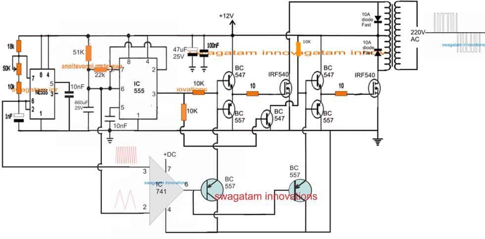
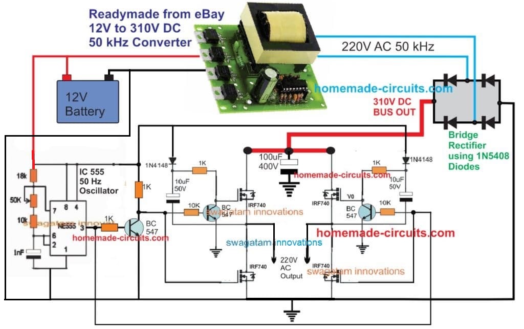
 Below is the schematic for the circuit.

 Circuit Objectives and Requirements
I would like to retrofit the rotating beacon grain tank level indicator system shown below, to my older combine harvester.
The particular part of the system I want to build is this:
Turns on automatically when the grain tank level reaches three-quarter.
Beacon lights begin an alternating pattern once the three-quarters full sensor is triggered; beacon lights remain on for 10 seconds then turn off for 10 second continually repeating until the grain tank full sensor is triggered.
Once the grain tank full sensor is triggered the beacon lights remain on constantly.
Would you be able to design a circuit to perform this function? I already have the bin level sensor, and it is a normally open type of contact.
The specs on the sensor are: 48V, .5amp, 10 watt, 300mA, so even though I��m planning on using LED beacon lights, I suspect the output of any circuit would have to trigger a relay to a power circuit for the beacons.
I would also like to be able to switch the system off from the control station of the combine.
Thanks in advance for any and all input!
Circuit Objectives and Requirements
I would like to retrofit the rotating beacon grain tank level indicator system shown below, to my older combine harvester.
The particular part of the system I want to build is this:
Turns on automatically when the grain tank level reaches three-quarter.
Beacon lights begin an alternating pattern once the three-quarters full sensor is triggered; beacon lights remain on for 10 seconds then turn off for 10 second continually repeating until the grain tank full sensor is triggered.
Once the grain tank full sensor is triggered the beacon lights remain on constantly.
Would you be able to design a circuit to perform this function? I already have the bin level sensor, and it is a normally open type of contact.
The specs on the sensor are: 48V, .5amp, 10 watt, 300mA, so even though I��m planning on using LED beacon lights, I suspect the output of any circuit would have to trigger a relay to a power circuit for the beacons.
I would also like to be able to switch the system off from the control station of the combine.
Thanks in advance for any and all input!

 The IC 555 is configured in its standard astable mode (flashing mode), where R1,R2, and C values determine the flashing rate of the IC at its pin#3.
These values are calculated to produce a reasonably precise 5 second ON/OFF switching on pin#3 of the IC.
The IC 555 is configured in its standard astable mode (flashing mode), where R1,R2, and C values determine the flashing rate of the IC at its pin#3.
These values are calculated to produce a reasonably precise 5 second ON/OFF switching on pin#3 of the IC.
 The desired delay period for which the relay and the solenoid should remain switched ON can be calculated using this IC 555 calculator software.
The above design only takes care of the timed solenoid operation in response to pressing of a button, however for implementing the design accurately as a tea/coffee vending machine circuit, it needs to be upgraded with a foolproof payment option, so that the customer is able to insert a legitimate 5 rupee coin for accessing the beverage.
The desired delay period for which the relay and the solenoid should remain switched ON can be calculated using this IC 555 calculator software.
The above design only takes care of the timed solenoid operation in response to pressing of a button, however for implementing the design accurately as a tea/coffee vending machine circuit, it needs to be upgraded with a foolproof payment option, so that the customer is able to insert a legitimate 5 rupee coin for accessing the beverage.
 The above circuit can be used for roughly determining the weight of the coin by allowing the coin to strike on an electret mic and then measuring the striking or vibrational force through a LM3915 circuit.
Heavier coin will supposedly create higher voltage spikes from the MIC output, and vice versa.
The difference in the intensity of the voltage spikes will hopefully create corresponding levels of voltage shifts across the output pins of the IC from pin#1 to pin#10.
The 10k preset at pin#5 is appropriately adjusted such that a genuine coin generates a spike that may reach around pin#13/14. This level would be held intact for so long as the 100uF capacitor is discharged.
Since the relay driver transistor BC557 is attached with the pin#13/14 of the IC, it should immediately conduct whenever a legitimate coin is inserted, and subsequently actuate the relay and the solenoid.
The solenoid actuation allows the person to collect the beverage in the form of tea or coffee in the cup.
In case a false imitation coin is inserted which may be lighter or heavier in mass might create a voltage spike either not sufficient to go up to pin13/14, and might only reach across the lower pinouts of the IC, or surpass the pn13/14 of the IC and trigger the upper irrelevant pinouts of the IC.
In either case the relay driver transistor would not activate thwarting the false attempt by the fake coin
The 100uF capacitor is arbitrarily selected, this needs to be tweaked with some trial and error to ensure that the relay activates for a period of time that may be just enough for filling the beverage cup up to its rim.
The above circuit can be used for roughly determining the weight of the coin by allowing the coin to strike on an electret mic and then measuring the striking or vibrational force through a LM3915 circuit.
Heavier coin will supposedly create higher voltage spikes from the MIC output, and vice versa.
The difference in the intensity of the voltage spikes will hopefully create corresponding levels of voltage shifts across the output pins of the IC from pin#1 to pin#10.
The 10k preset at pin#5 is appropriately adjusted such that a genuine coin generates a spike that may reach around pin#13/14. This level would be held intact for so long as the 100uF capacitor is discharged.
Since the relay driver transistor BC557 is attached with the pin#13/14 of the IC, it should immediately conduct whenever a legitimate coin is inserted, and subsequently actuate the relay and the solenoid.
The solenoid actuation allows the person to collect the beverage in the form of tea or coffee in the cup.
In case a false imitation coin is inserted which may be lighter or heavier in mass might create a voltage spike either not sufficient to go up to pin13/14, and might only reach across the lower pinouts of the IC, or surpass the pn13/14 of the IC and trigger the upper irrelevant pinouts of the IC.
In either case the relay driver transistor would not activate thwarting the false attempt by the fake coin
The 100uF capacitor is arbitrarily selected, this needs to be tweaked with some trial and error to ensure that the relay activates for a period of time that may be just enough for filling the beverage cup up to its rim.
 In the above set up we can see how the proposed MIC needs to be arranged along with a channelized guide for enabling the coin to slide down to the destination from its drop slot.
The channel or the pipe through which coin must pass can be seen connected with a strong electromagnet from the outer side of the tube.
This electromagnet needs to be continuously switched ON throughout the operational period of the machine, so that in case a fake coin (made up of iron or steel) is inserted, it gets caught with the electromagnet and the beverage is never made available to the person attempting the theft.
If you have any doubts or questions regarding the above explained tea, coffee vending machine circuit, you may feel fee to ask the same through the comments.
In the above set up we can see how the proposed MIC needs to be arranged along with a channelized guide for enabling the coin to slide down to the destination from its drop slot.
The channel or the pipe through which coin must pass can be seen connected with a strong electromagnet from the outer side of the tube.
This electromagnet needs to be continuously switched ON throughout the operational period of the machine, so that in case a fake coin (made up of iron or steel) is inserted, it gets caught with the electromagnet and the beverage is never made available to the person attempting the theft.
If you have any doubts or questions regarding the above explained tea, coffee vending machine circuit, you may feel fee to ask the same through the comments.
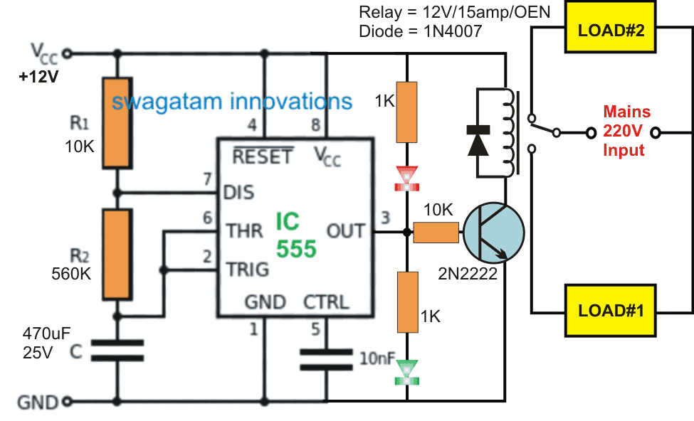 The circuit is built around a standard IC 555 astable configuration, which basically produces an alternating high and low or an alternating 12V and zero volt at its pin#3 when switched ON.
This alternately switching output accompanies certain delay between its ON/OFF switching as determined by the component values of R1, R2, and C.
In the proposed design the values of these timing components are suitably calculated to produce an approximately 50% duty cycle, and having a delay length of around 180 seconds or 3 minutes.
With the shown arrangement, only the value of the 470uF capacitor needs to be altered for achieving other preferred time delays across the output pin#3.
The pin#3 can be seen connected with a transistor relay driver stage which responds to the high/low pulses from the pinout and accordingly switches the relay contacts across the N/C and N/O contacts.
Since the two loads are connected across these two contacts of the relay, these are also alternately switched from ON to OFF and vice versa with a delay of 3 minutes between each switching.
The two LEDs connected across the supply pins and the pin#3 of the IC helps to indicate which load may be in the switched ON or OFF position at a given instant.
The above explained alternate switching relay timer circuit can be also implemented for other identical applications and the ON/OFF periods can be independently adjusted for achieving different ON/OFF sequences, by suitably altering the R1/R2 timing components of the astable.
The circuit is built around a standard IC 555 astable configuration, which basically produces an alternating high and low or an alternating 12V and zero volt at its pin#3 when switched ON.
This alternately switching output accompanies certain delay between its ON/OFF switching as determined by the component values of R1, R2, and C.
In the proposed design the values of these timing components are suitably calculated to produce an approximately 50% duty cycle, and having a delay length of around 180 seconds or 3 minutes.
With the shown arrangement, only the value of the 470uF capacitor needs to be altered for achieving other preferred time delays across the output pin#3.
The pin#3 can be seen connected with a transistor relay driver stage which responds to the high/low pulses from the pinout and accordingly switches the relay contacts across the N/C and N/O contacts.
Since the two loads are connected across these two contacts of the relay, these are also alternately switched from ON to OFF and vice versa with a delay of 3 minutes between each switching.
The two LEDs connected across the supply pins and the pin#3 of the IC helps to indicate which load may be in the switched ON or OFF position at a given instant.
The above explained alternate switching relay timer circuit can be also implemented for other identical applications and the ON/OFF periods can be independently adjusted for achieving different ON/OFF sequences, by suitably altering the R1/R2 timing components of the astable.
 The left side green board is the remote receiver module having the six control relays and this units needs to be installed inside the RC helicopter for the necessary control operations.
The right side unit is the transmitter handset which is supposed to be held by the user and the relevant buttons pressed for commanding the relay board with the corresponding motion control info.
Now lets see how the six relays needs to be configured with the various PWM circuits and installed inside the RC chopper, from the following details:
Remember the relay contacts shown in the receiver board are all blank by default, meaning their N/C and N/O contacts are not wired and must be wired as illustrated in the following diagrams.
According to the request, the 9V motor and the 12V motor speeds need to be controlled through the subsequent pressing of the remote handset.
The circuits for implementing this function are shown below:
The left side green board is the remote receiver module having the six control relays and this units needs to be installed inside the RC helicopter for the necessary control operations.
The right side unit is the transmitter handset which is supposed to be held by the user and the relevant buttons pressed for commanding the relay board with the corresponding motion control info.
Now lets see how the six relays needs to be configured with the various PWM circuits and installed inside the RC chopper, from the following details:
Remember the relay contacts shown in the receiver board are all blank by default, meaning their N/C and N/O contacts are not wired and must be wired as illustrated in the following diagrams.
According to the request, the 9V motor and the 12V motor speeds need to be controlled through the subsequent pressing of the remote handset.
The circuits for implementing this function are shown below:


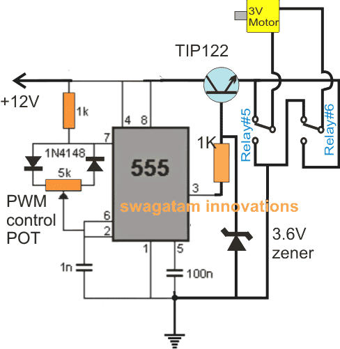 Here also we employ the versatile IC 555 wired as a precise PWM generator circuit.
The PWM is set appropriately through the 5K preset before finalizing the installations such that the speed of the motor is perfectly adjusted for the required equilibrium of the helicopter.
The relays can be seen simply wired to enforce the required reverse, and forward or a clockwise or anticlockwise motion for the motor in response to the toggling of the paired relay contact, which together form a DPDT relay.
In order to prevent a short circuit, preferably the receiver module should be modified for these two relays such that pressing either of the buttons causes both the relays to activate together rather tan depending on two switches to be pressed in sync for the activation.
This toggling can be expected to flip the motor rotation in the opposite direction instantly allowing the user to execute the required directional changes in the RC helicopter machine.
This concludes the circuit and relay wiring instructions for the proposed RC helicopter remote control circuit, for further doubts please do not hesitate to express them through your comments.
Here also we employ the versatile IC 555 wired as a precise PWM generator circuit.
The PWM is set appropriately through the 5K preset before finalizing the installations such that the speed of the motor is perfectly adjusted for the required equilibrium of the helicopter.
The relays can be seen simply wired to enforce the required reverse, and forward or a clockwise or anticlockwise motion for the motor in response to the toggling of the paired relay contact, which together form a DPDT relay.
In order to prevent a short circuit, preferably the receiver module should be modified for these two relays such that pressing either of the buttons causes both the relays to activate together rather tan depending on two switches to be pressed in sync for the activation.
This toggling can be expected to flip the motor rotation in the opposite direction instantly allowing the user to execute the required directional changes in the RC helicopter machine.
This concludes the circuit and relay wiring instructions for the proposed RC helicopter remote control circuit, for further doubts please do not hesitate to express them through your comments.
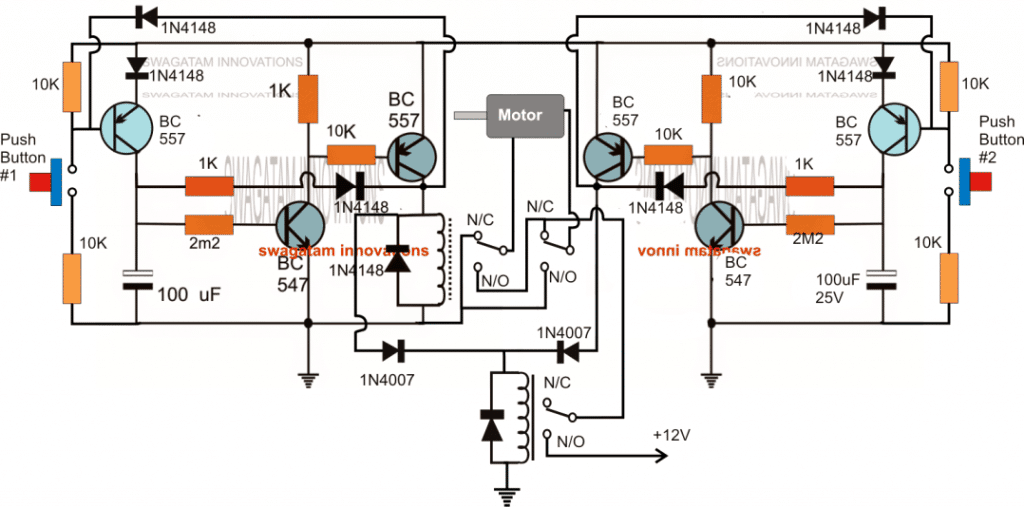
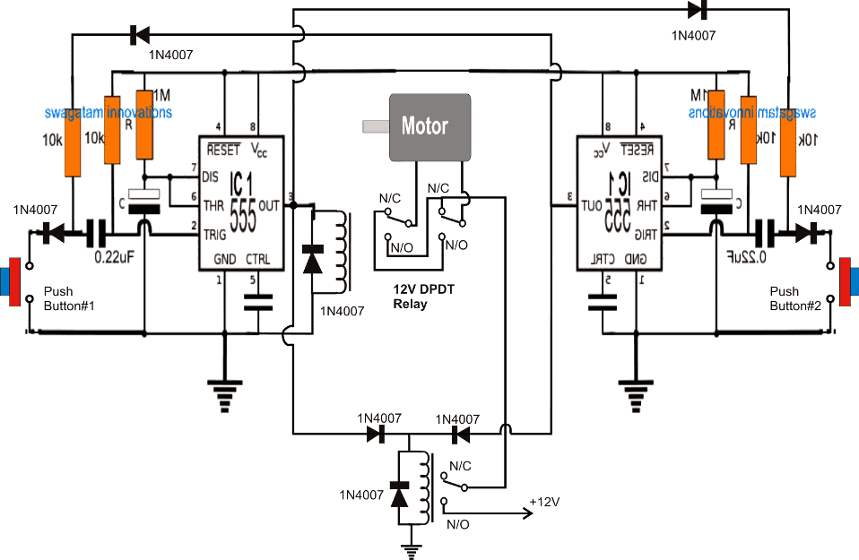
 1) Basically the machine requires a firm and strong body, but extremely light in weight.
This could be fabricated or assembled using hollow square aluminum extrusion pipes, by suitably drilling holes and fixing the frame with nuts and bolts.
2) The structure should be in the form of a perfect "+" or a perfect "x", it doesn't make a difference as long as the angle between the "crossing" pipes are at 90 degrees each.
1) Basically the machine requires a firm and strong body, but extremely light in weight.
This could be fabricated or assembled using hollow square aluminum extrusion pipes, by suitably drilling holes and fixing the frame with nuts and bolts.
2) The structure should be in the form of a perfect "+" or a perfect "x", it doesn't make a difference as long as the angle between the "crossing" pipes are at 90 degrees each.
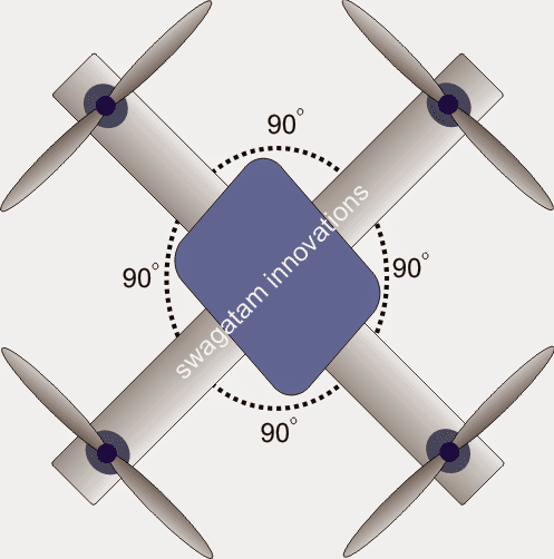 Basic elements needed for constructing a quadcopter can be seen in the following image:


 As indicated in the above diagrams, by appropriately decreasing the speed of a set of motors, or increasing the speed of the opposite set of motors, or tweaking the speeds as per ones own preference the quadcopter can be made to travel in the air in any desired specific direction.
The above images indicate the basic directions, such as forward, reverse, right, left etc...however any other odd direction can also be efficiently implemented by suitably adjusting the speeds of the relevant motors or may be just a single motor.
For example in order to force the machine to fly towards the N/W direction, the speed of only the S/E motor may be increased, and for enabling the machine to fly at the N/E direction, the speed of the S/W motor may be increased...and so on.
It just needs to be practiced until the full control of the quadcopter becomes achievable and mastered by the user.
As indicated in the above diagrams, by appropriately decreasing the speed of a set of motors, or increasing the speed of the opposite set of motors, or tweaking the speeds as per ones own preference the quadcopter can be made to travel in the air in any desired specific direction.
The above images indicate the basic directions, such as forward, reverse, right, left etc...however any other odd direction can also be efficiently implemented by suitably adjusting the speeds of the relevant motors or may be just a single motor.
For example in order to force the machine to fly towards the N/W direction, the speed of only the S/E motor may be increased, and for enabling the machine to fly at the N/E direction, the speed of the S/W motor may be increased...and so on.
It just needs to be practiced until the full control of the quadcopter becomes achievable and mastered by the user.
 You will need to buy these RF modules from any online store or from your local electronic spare dealer:
Apart from the above mentioned RF remotes modules 4 permanent magnet brushed motors will be also required which actually forms the heart of the drone machine.
It could be as specified in the following image with the given descriptions, or any other similar as per the required user specifications:
You will need to buy these RF modules from any online store or from your local electronic spare dealer:
Apart from the above mentioned RF remotes modules 4 permanent magnet brushed motors will be also required which actually forms the heart of the drone machine.
It could be as specified in the following image with the given descriptions, or any other similar as per the required user specifications:
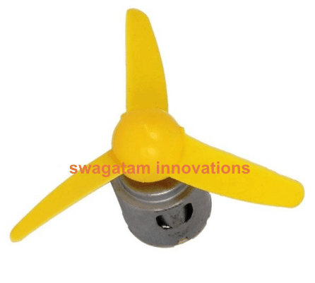 Electrical Specifications of the Motor:
6V = operating voltage (peak 12V)
200mA = operating current
10,000 = RPM
Electrical Specifications of the Motor:
6V = operating voltage (peak 12V)
200mA = operating current
10,000 = RPM
 Referring to the above diagram we realize that we simply need to appropriately increase the speeds of the relevant motors for executing the desired directional maneuvers on the drone.
This increase of speeds can be enforced by configuring the remote control relays as per the following wiring diagram.
In the diagram below we can see an IC 555 PWM circuit wired with the 4 relays of the remote control receiver module of the 6 relays (1 relay being unused and could be simply removed to educe space and weight).
Referring to the above diagram we realize that we simply need to appropriately increase the speeds of the relevant motors for executing the desired directional maneuvers on the drone.
This increase of speeds can be enforced by configuring the remote control relays as per the following wiring diagram.
In the diagram below we can see an IC 555 PWM circuit wired with the 4 relays of the remote control receiver module of the 6 relays (1 relay being unused and could be simply removed to educe space and weight).
 The shown relays are the part of the RF module receiver, whose contacts are initially unconnected (blank by default) and needs to be wired as indicated in the above diagram.
The RF remote receiver is supposed to be installed inside the quadcopter and its relays wired with the relevant motors and battery as per the above shown layout.
You can see a few connectors (green colored) which can unnecessarily add weight on the drone.
You can remove them all to reduce weight, and connect the relevant wires directly to the PCB by soldering.
The shown relays are the part of the RF module receiver, whose contacts are initially unconnected (blank by default) and needs to be wired as indicated in the above diagram.
The RF remote receiver is supposed to be installed inside the quadcopter and its relays wired with the relevant motors and battery as per the above shown layout.
You can see a few connectors (green colored) which can unnecessarily add weight on the drone.
You can remove them all to reduce weight, and connect the relevant wires directly to the PCB by soldering.